JP4405024B2 - Semiconductor device - Google Patents
Semiconductor device Download PDFInfo
- Publication number
- JP4405024B2 JP4405024B2 JP2000009208A JP2000009208A JP4405024B2 JP 4405024 B2 JP4405024 B2 JP 4405024B2 JP 2000009208 A JP2000009208 A JP 2000009208A JP 2000009208 A JP2000009208 A JP 2000009208A JP 4405024 B2 JP4405024 B2 JP 4405024B2
- Authority
- JP
- Japan
- Prior art keywords
- layer
- signal
- plane
- conductor layer
- core
- Prior art date
- Legal status (The legal status is an assumption and is not a legal conclusion. Google has not performed a legal analysis and makes no representation as to the accuracy of the status listed.)
- Expired - Fee Related
Links
Images


Classifications
-
- H—ELECTRICITY
- H01—ELECTRIC ELEMENTS
- H01L—SEMICONDUCTOR DEVICES NOT COVERED BY CLASS H10
- H01L21/00—Processes or apparatus adapted for the manufacture or treatment of semiconductor or solid state devices or of parts thereof
- H01L21/02—Manufacture or treatment of semiconductor devices or of parts thereof
- H01L21/04—Manufacture or treatment of semiconductor devices or of parts thereof the devices having at least one potential-jump barrier or surface barrier, e.g. PN junction, depletion layer or carrier concentration layer
- H01L21/50—Assembly of semiconductor devices using processes or apparatus not provided for in a single one of the subgroups H01L21/06 - H01L21/326, e.g. sealing of a cap to a base of a container
- H01L21/56—Encapsulations, e.g. encapsulation layers, coatings
- H01L21/563—Encapsulation of active face of flip-chip device, e.g. underfilling or underencapsulation of flip-chip, encapsulation preform on chip or mounting substrate
-
- H—ELECTRICITY
- H01—ELECTRIC ELEMENTS
- H01L—SEMICONDUCTOR DEVICES NOT COVERED BY CLASS H10
- H01L21/00—Processes or apparatus adapted for the manufacture or treatment of semiconductor or solid state devices or of parts thereof
- H01L21/02—Manufacture or treatment of semiconductor devices or of parts thereof
- H01L21/04—Manufacture or treatment of semiconductor devices or of parts thereof the devices having at least one potential-jump barrier or surface barrier, e.g. PN junction, depletion layer or carrier concentration layer
- H01L21/50—Assembly of semiconductor devices using processes or apparatus not provided for in a single one of the subgroups H01L21/06 - H01L21/326, e.g. sealing of a cap to a base of a container
- H01L21/60—Attaching or detaching leads or other conductive members, to be used for carrying current to or from the device in operation
-
- H—ELECTRICITY
- H01—ELECTRIC ELEMENTS
- H01L—SEMICONDUCTOR DEVICES NOT COVERED BY CLASS H10
- H01L23/00—Details of semiconductor or other solid state devices
- H01L23/48—Arrangements for conducting electric current to or from the solid state body in operation, e.g. leads, terminal arrangements ; Selection of materials therefor
- H01L23/488—Arrangements for conducting electric current to or from the solid state body in operation, e.g. leads, terminal arrangements ; Selection of materials therefor consisting of soldered or bonded constructions
- H01L23/498—Leads, i.e. metallisations or lead-frames on insulating substrates, e.g. chip carriers
- H01L23/49811—Additional leads joined to the metallisation on the insulating substrate, e.g. pins, bumps, wires, flat leads
- H01L23/49816—Spherical bumps on the substrate for external connection, e.g. ball grid arrays [BGA]
-
- H—ELECTRICITY
- H01—ELECTRIC ELEMENTS
- H01L—SEMICONDUCTOR DEVICES NOT COVERED BY CLASS H10
- H01L23/00—Details of semiconductor or other solid state devices
- H01L23/48—Arrangements for conducting electric current to or from the solid state body in operation, e.g. leads, terminal arrangements ; Selection of materials therefor
- H01L23/488—Arrangements for conducting electric current to or from the solid state body in operation, e.g. leads, terminal arrangements ; Selection of materials therefor consisting of soldered or bonded constructions
- H01L23/498—Leads, i.e. metallisations or lead-frames on insulating substrates, e.g. chip carriers
- H01L23/49827—Via connections through the substrates, e.g. pins going through the substrate, coaxial cables
-
- H—ELECTRICITY
- H01—ELECTRIC ELEMENTS
- H01L—SEMICONDUCTOR DEVICES NOT COVERED BY CLASS H10
- H01L23/00—Details of semiconductor or other solid state devices
- H01L23/48—Arrangements for conducting electric current to or from the solid state body in operation, e.g. leads, terminal arrangements ; Selection of materials therefor
- H01L23/488—Arrangements for conducting electric current to or from the solid state body in operation, e.g. leads, terminal arrangements ; Selection of materials therefor consisting of soldered or bonded constructions
- H01L23/498—Leads, i.e. metallisations or lead-frames on insulating substrates, e.g. chip carriers
- H01L23/49833—Leads, i.e. metallisations or lead-frames on insulating substrates, e.g. chip carriers the chip support structure consisting of a plurality of insulating substrates
-
- H—ELECTRICITY
- H01—ELECTRIC ELEMENTS
- H01L—SEMICONDUCTOR DEVICES NOT COVERED BY CLASS H10
- H01L2224/00—Indexing scheme for arrangements for connecting or disconnecting semiconductor or solid-state bodies and methods related thereto as covered by H01L24/00
- H01L2224/01—Means for bonding being attached to, or being formed on, the surface to be connected, e.g. chip-to-package, die-attach, "first-level" interconnects; Manufacturing methods related thereto
- H01L2224/10—Bump connectors; Manufacturing methods related thereto
- H01L2224/15—Structure, shape, material or disposition of the bump connectors after the connecting process
- H01L2224/16—Structure, shape, material or disposition of the bump connectors after the connecting process of an individual bump connector
- H01L2224/161—Disposition
- H01L2224/16151—Disposition the bump connector connecting between a semiconductor or solid-state body and an item not being a semiconductor or solid-state body, e.g. chip-to-substrate, chip-to-passive
- H01L2224/16221—Disposition the bump connector connecting between a semiconductor or solid-state body and an item not being a semiconductor or solid-state body, e.g. chip-to-substrate, chip-to-passive the body and the item being stacked
- H01L2224/16225—Disposition the bump connector connecting between a semiconductor or solid-state body and an item not being a semiconductor or solid-state body, e.g. chip-to-substrate, chip-to-passive the body and the item being stacked the item being non-metallic, e.g. insulating substrate with or without metallisation
-
- H—ELECTRICITY
- H01—ELECTRIC ELEMENTS
- H01L—SEMICONDUCTOR DEVICES NOT COVERED BY CLASS H10
- H01L2224/00—Indexing scheme for arrangements for connecting or disconnecting semiconductor or solid-state bodies and methods related thereto as covered by H01L24/00
- H01L2224/01—Means for bonding being attached to, or being formed on, the surface to be connected, e.g. chip-to-package, die-attach, "first-level" interconnects; Manufacturing methods related thereto
- H01L2224/26—Layer connectors, e.g. plate connectors, solder or adhesive layers; Manufacturing methods related thereto
- H01L2224/31—Structure, shape, material or disposition of the layer connectors after the connecting process
- H01L2224/32—Structure, shape, material or disposition of the layer connectors after the connecting process of an individual layer connector
- H01L2224/321—Disposition
- H01L2224/32151—Disposition the layer connector connecting between a semiconductor or solid-state body and an item not being a semiconductor or solid-state body, e.g. chip-to-substrate, chip-to-passive
- H01L2224/32221—Disposition the layer connector connecting between a semiconductor or solid-state body and an item not being a semiconductor or solid-state body, e.g. chip-to-substrate, chip-to-passive the body and the item being stacked
- H01L2224/32225—Disposition the layer connector connecting between a semiconductor or solid-state body and an item not being a semiconductor or solid-state body, e.g. chip-to-substrate, chip-to-passive the body and the item being stacked the item being non-metallic, e.g. insulating substrate with or without metallisation
-
- H—ELECTRICITY
- H01—ELECTRIC ELEMENTS
- H01L—SEMICONDUCTOR DEVICES NOT COVERED BY CLASS H10
- H01L2224/00—Indexing scheme for arrangements for connecting or disconnecting semiconductor or solid-state bodies and methods related thereto as covered by H01L24/00
- H01L2224/73—Means for bonding being of different types provided for in two or more of groups H01L2224/10, H01L2224/18, H01L2224/26, H01L2224/34, H01L2224/42, H01L2224/50, H01L2224/63, H01L2224/71
- H01L2224/732—Location after the connecting process
- H01L2224/73201—Location after the connecting process on the same surface
- H01L2224/73203—Bump and layer connectors
- H01L2224/73204—Bump and layer connectors the bump connector being embedded into the layer connector
-
- H—ELECTRICITY
- H01—ELECTRIC ELEMENTS
- H01L—SEMICONDUCTOR DEVICES NOT COVERED BY CLASS H10
- H01L2224/00—Indexing scheme for arrangements for connecting or disconnecting semiconductor or solid-state bodies and methods related thereto as covered by H01L24/00
- H01L2224/73—Means for bonding being of different types provided for in two or more of groups H01L2224/10, H01L2224/18, H01L2224/26, H01L2224/34, H01L2224/42, H01L2224/50, H01L2224/63, H01L2224/71
- H01L2224/732—Location after the connecting process
- H01L2224/73251—Location after the connecting process on different surfaces
- H01L2224/73253—Bump and layer connectors
-
- H—ELECTRICITY
- H01—ELECTRIC ELEMENTS
- H01L—SEMICONDUCTOR DEVICES NOT COVERED BY CLASS H10
- H01L2924/00—Indexing scheme for arrangements or methods for connecting or disconnecting semiconductor or solid-state bodies as covered by H01L24/00
- H01L2924/01—Chemical elements
- H01L2924/01078—Platinum [Pt]
-
- H—ELECTRICITY
- H01—ELECTRIC ELEMENTS
- H01L—SEMICONDUCTOR DEVICES NOT COVERED BY CLASS H10
- H01L2924/00—Indexing scheme for arrangements or methods for connecting or disconnecting semiconductor or solid-state bodies as covered by H01L24/00
- H01L2924/15—Details of package parts other than the semiconductor or other solid state devices to be connected
- H01L2924/151—Die mounting substrate
- H01L2924/1517—Multilayer substrate
- H01L2924/15172—Fan-out arrangement of the internal vias
- H01L2924/15173—Fan-out arrangement of the internal vias in a single layer of the multilayer substrate
-
- H—ELECTRICITY
- H01—ELECTRIC ELEMENTS
- H01L—SEMICONDUCTOR DEVICES NOT COVERED BY CLASS H10
- H01L2924/00—Indexing scheme for arrangements or methods for connecting or disconnecting semiconductor or solid-state bodies as covered by H01L24/00
- H01L2924/15—Details of package parts other than the semiconductor or other solid state devices to be connected
- H01L2924/151—Die mounting substrate
- H01L2924/1517—Multilayer substrate
- H01L2924/15172—Fan-out arrangement of the internal vias
- H01L2924/15174—Fan-out arrangement of the internal vias in different layers of the multilayer substrate
-
- H—ELECTRICITY
- H01—ELECTRIC ELEMENTS
- H01L—SEMICONDUCTOR DEVICES NOT COVERED BY CLASS H10
- H01L2924/00—Indexing scheme for arrangements or methods for connecting or disconnecting semiconductor or solid-state bodies as covered by H01L24/00
- H01L2924/15—Details of package parts other than the semiconductor or other solid state devices to be connected
- H01L2924/151—Die mounting substrate
- H01L2924/153—Connection portion
- H01L2924/1531—Connection portion the connection portion being formed only on the surface of the substrate opposite to the die mounting surface
- H01L2924/15311—Connection portion the connection portion being formed only on the surface of the substrate opposite to the die mounting surface being a ball array, e.g. BGA
-
- H—ELECTRICITY
- H01—ELECTRIC ELEMENTS
- H01L—SEMICONDUCTOR DEVICES NOT COVERED BY CLASS H10
- H01L2924/00—Indexing scheme for arrangements or methods for connecting or disconnecting semiconductor or solid-state bodies as covered by H01L24/00
- H01L2924/15—Details of package parts other than the semiconductor or other solid state devices to be connected
- H01L2924/161—Cap
- H01L2924/1615—Shape
- H01L2924/16195—Flat cap [not enclosing an internal cavity]
-
- H—ELECTRICITY
- H05—ELECTRIC TECHNIQUES NOT OTHERWISE PROVIDED FOR
- H05K—PRINTED CIRCUITS; CASINGS OR CONSTRUCTIONAL DETAILS OF ELECTRIC APPARATUS; MANUFACTURE OF ASSEMBLAGES OF ELECTRICAL COMPONENTS
- H05K1/00—Printed circuits
- H05K1/02—Details
- H05K1/0213—Electrical arrangements not otherwise provided for
- H05K1/0216—Reduction of cross-talk, noise or electromagnetic interference
- H05K1/0218—Reduction of cross-talk, noise or electromagnetic interference by printed shielding conductors, ground planes or power plane
-
- H—ELECTRICITY
- H05—ELECTRIC TECHNIQUES NOT OTHERWISE PROVIDED FOR
- H05K—PRINTED CIRCUITS; CASINGS OR CONSTRUCTIONAL DETAILS OF ELECTRIC APPARATUS; MANUFACTURE OF ASSEMBLAGES OF ELECTRICAL COMPONENTS
- H05K1/00—Printed circuits
- H05K1/02—Details
- H05K1/11—Printed elements for providing electric connections to or between printed circuits
- H05K1/111—Pads for surface mounting, e.g. lay-out
- H05K1/112—Pads for surface mounting, e.g. lay-out directly combined with via connections
-
- H—ELECTRICITY
- H05—ELECTRIC TECHNIQUES NOT OTHERWISE PROVIDED FOR
- H05K—PRINTED CIRCUITS; CASINGS OR CONSTRUCTIONAL DETAILS OF ELECTRIC APPARATUS; MANUFACTURE OF ASSEMBLAGES OF ELECTRICAL COMPONENTS
- H05K3/00—Apparatus or processes for manufacturing printed circuits
- H05K3/46—Manufacturing multilayer circuits
- H05K3/4602—Manufacturing multilayer circuits characterized by a special circuit board as base or central core whereon additional circuit layers are built or additional circuit boards are laminated
Description
【0001】
【発明の属する技術分野】
この発明は、電源プレーン、グランドプレーンおよび信号線を多層的に配置した多層基板を用いた半導体装置に関するものである。
【0002】
【従来の技術】
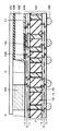
従来の半導体装置の一例を図9、図10に示す。この半導体装置は、FCBGA(Flip Chip Ball Grid Array)基板と呼ばれるものである。ただし、以下、基板部分単体との混同を避けるために、このパッケージ全体を「FCBGA基板モジュール」100という。この半導体装置は、BGA(Ball Grid Array)基板101と、このBGA基板101と電極としてのはんだバンプ105を介してフリップチップ接合された半導体チップ102を備えている。BGA基板101は多層構造からなる基板であって、外部と電気的接続を得るために裏面に外部接続電極としてのはんだボール106が配列されている。BGA基板101と半導体チップ102との間には、両者間の接合の信頼性を向上させるための封止材104が充填されている。また、半導体チップ102の上方には、半導体チップ102から発生した熱を外部に放熱するために放熱樹脂108を介在してヒートスプレッダ107が設けられている。放熱樹脂108は、半導体チップ102からヒートスプレッダ107への放熱を促進するためのものである。BGA基板101とヒートスプレッダ107との間の所定の間隔を保持し、かつパッケージ全体の強度を持たせるために、半導体チップ102を取囲むようにリング103が設けられている。
【0003】
なお、図9では、内部の構造をわかりやすくするために、ヒートスプレッダ107の一部を取り去った状態で図示している。また、図9、図10とも模式図であり、わかりやすくするために、寸法比率を誇張し、はんだバンプ105やはんだボール106の個数を、省略して表示している。
【0004】
図10の左半分に相当する部分を拡大し、より詳細に示したものを、図11に示す。多層基板であるBGA基板101は、たとえば、BTレジンから形成されるコア層8の両面にメッキにより形成された銅のプレーン13,14を有するプレーン層10,11を備え、さらにその両面に均等に積層された複数の層から形成されている。これらの複数の層については、便宜上、コア層8より上側の部分を「上多層部」、コア層8より下側の部分を「下多層部」と呼ぶものとする。
この上多層部および下多層部の中には、信号層9、電源プレーン層10、グランドプレーン層11が一定の順序でほぼ等間隔に挿入されている。これらの挿入された各層を以下、「構成層」というものとする。
【0005】
信号層9とは、信号線12の横方向への布設、すなわちいわゆる「引き回し」を行なうことを主目的とする層である。電源プレーン層10とは、電源を供給するための導電体のプレーンである電源プレーンを配置することを主目的とする層である。グランドプレーン層11とは、接地した導電体のプレーンであるグランドプレーンを配置することを主目的とする層である。
【0006】
半導体チップ102の電極としてのはんだバンプ105は、その役割によって、信号用はんだバンプ105aと非信号用はんだバンプ105bとの2種類に分類することができる。信号用はんだバンプ105aは、信号をやりとりするためのはんだバンプ105であって、いずれかのはんだボール106と電気的に接続されている。非信号用はんだバンプ105bは、通常、電源プレーン13やグランドプレーン14に接続されている。
【0007】
信号用はんだバンプ105aからはんだボール106への接続は、上多層部、コア層8、下多層部を順に経て、行なう必要があるが、同一層内での横方向への布設は、信号線12の引き回しによって行なわれ、下の層への接続は、ビアホール17によって行われている。
【0008】
信号線12を一つの信号層9内に配置する際には、上下の信号線12との間のクロストークノイズを防止するために、信号層9をプレーン層で挟み込む、いわゆるストリップ構造をとることが原則とされる。したがって、図11に示すように、最も上の構成層を第1の信号層9とした場合、その一つ下の構成層には、プレーン層の1種であるグランドプレーン層11が配置される。そのさらに下に第2の信号層9が配置される。さらにその下にはプレーン層の1種である電源プレーン層10が配置されている。
【0009】
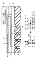
このFCBGA基板モジュールの例では、はんだバンプ105は、半導体チップ102の下面のうち、周縁部のみにほぼ帯状に配置されている。そのうち、帯の幅方向に数えた信号用はんだバンプ105aの列数は6〜7である。これらの電極に対するチップ電極用ランドとしての信号用はんだバンプランド16aの配置もこれと同じである。信号用はんだバンプランド16aをそれぞれはんだボール106に何らかの経路によって接続する必要がある。この接続の様子を図12〜図14を参照して説明する。図12、図13は、信号の流れを記号化して表したものであって、1つの構成層内の複数の信号線12は、本来紙面の手前・奥方向に2次元的に展開しているため同一断面には表れないものであるが、わかりやすくするために、1つの層内に並列して表示している。図14は、図11、図12における最も上の信号層9を上方向から見た平面図に相当する模式図である。
【0010】
図12、図14に示すように、1つの信号層9ごとに、信号用はんだバンプランド16aの並びのうち外側から優先的に2〜3列ずつを受け持つこととし、その1つの信号層9において半導体チップ102の投影領域102c(図14参照)からその外へ向かって信号線12によって引き回されている。この信号線12は、いずれかのはんだボール106に接続されるためには、いずれかのスルーホール15を経由する必要がある。しかし、各構成層における配線の配置ピッチが、配線外縁同士の最低確保すべき距離が数十μmとなっているのに比べて、スルーホール15の配列ピッチは中心間距離で約800μmという、何倍も粗い配置となっている。そのため、引き出された信号線12は、図14に示すように、その信号層9内で、目的とするはんだボール106に対応する位置の近傍まで引き回され、そこからビアホール17とスルーホール15とを介して下の層へと接続されていく。後から引き回される信号線12との間で互いに別個のスルーホール15を使う必要があることと、配線の混雑を避けるため、先に引き回しの行われた信号線12ほど、投影領域102cから遠くのスルーホール15を経由する。
【0011】
一方、その信号層9で外へ引き回されなかった信号用はんだバンプ16aについては、図12に示すようにその信号層9からビアホール17を介してより下の信号層9へとそれぞれ接続され、受け持たれるべき信号層9に到達した時点で、信号線12によって横方向への引き回しが行われる。
【0012】
図12、図13に示すように、この例では、上多層部と下多層部とを合わせて、3つの信号層9ですべての信号用バンプからの接続を分担して受け持っている。このとき上述のストリップ構造を維持しなければならないことと、コア層8の上下に向かって上多層部と下多層部とは対称に形成されていることにより、最下層のはんだボール106を備える層を含めて8層の構成層が必要となっている。
【0013】
なお、1つの信号層当り、信号用はんだバンプランド16aの2〜3列に相当する分ずつしか信号線12を引き回せないのは、図14に示すように、信号用はんだバンプランド16aの配置自体が密集しているうえ、信号用はんだバンプランド16aの外側には非信号用はんだバンプランド16bが配置されているため、信号線12がこれらと干渉しないように回避して、限られた面積で信号線12の配置を行なわなければならないためである。
【0014】
非信号用はんだバンプランド16bからは、図11に示すように、同一の構成層または他の構成層に存在する電源プレーン13やグランドプレーン14に向けて配線が設けられているが、図12ではその配線の図示を省略している。信号線12はこれらの配線と常に一定以上の距離を保つようにして隙間を縫って引き回す必要がある。
【0015】
【発明が解決しようとする課題】
このような半導体装置において、多層基板101の製造工程を省き、製造コストを低減するために、上多層部および下多層部として積み重ねる構成層の数を少なくすることが望まれている。しかし、信号用はんだバンプ105aの配列が変わらない限り、すべての信号用はんだバンプランド16aから信号線12の引き回しを行なうには、この例の場合、3つの信号層9が必要であり、また、クロストークノイズを防止するためにストリップ構造を維持する必要もある。
【0016】
そこで、本発明においては、信号用はんだバンプ105aの配列を従来のままで、多層基板101に必要な構成層の数を少なくした半導体装置を提供することを目的とする。
【0017】
【課題を解決するための手段】
上記目的を達成するため、本発明に基づく半導体装置の一つの局面においては、多層基板と、上記多層基板の上側に設けられた半導体チップと、上記多層基板の下側に設けられた外部接続電極とを備える。上記多層基板は、上面側と下面側とを電気的に接続するための複数のスルーホールを有するコア層と、上記コア層の上側に設けられた上多層部と、上記コア層の下側に設けられた下多層部と、上記半導体チップの電極と電気的に接続するために上記上多層部の上面に設けられた複数のチップ電極用ランドと、上記チップ電極用ランドと上記外部接続電極とをそれぞれ電気的に接続するための複数の信号線とを備える。上記上多層部および上記下多層部は、それぞれ複数の構成層からなるとともに、異なる上記構成層に属する上記信号線同士を電気的に接続するためのビアホールを含む。上記複数の構成層は、上記信号線を各同一層内で所望の平面的位置まで引き回すことを主目的とする信号層と、上記信号層を隣接してはさむ導電体のプレーンを配置することを主目的とするプレーン層とを含む。上記上多層部における上記信号層は、第1特定信号層と、上記第1特定信号層の下側に上記プレーン層を介さずに隣接する、第2特定信号層とを含む。上記第1特定信号層において上記半導体チップの投影領域内からその領域外へ引き出される上記信号線は、上記第1特定信号層において引き出される上記信号線すべてのうちの最長のものの距離が最短になるようにそれぞれ選択された上記スルーホールにつながる上記ビアホールまで引き出され、上記スルーホールを介して上記下多層部に接続され、さらに上記下多層部において、上記信号線が接続されるべき上記外部接続電極につながる上記ビアホールまで引き回されている。上記第2特定信号層において上記半導体チップの投影領域内からその領域外へ引き出される上記信号線は、上方から見たときに上記信号線が接続されるべき上記外部接続電極にほぼ最も近い上記スルーホールにつながる上記ビアホールまで引き出され、上記スルーホールを介して上記下多層部に接続されている。上記第1特定信号層において、上記信号線が配置されている部分以外の領域には導電体のプレーンを配置している。
【0018】
上記構成を採用することにより、第1特定信号層の信号線をそのまま第1特定信号層内で引き回さずに、一定条件下で選択されるスルーホールを経由して、下多層部に接続しているため、従来、余裕のあった下多層部の信号層のスペースを有効活用して信号線の引き回しを行なうことができる、また、第1特定信号層においては、ほぼ最小限の距離を引き回すのみであるため、第2特定信号層との間のクロストークノイズは問題とはならず、第1の信号層9と第2の信号層9との間のプレーン層を省略することができる。その結果、多層基板の層数の低減が可能となる。
【0019】
上記発明において好ましくは、上記第1特定信号層が、上記上多層部のうち最も上に位置する上記構成層である。この構成を採用することにより、少ない層数の多層基板においても、さらに層数を低減することができる。
【0020】
上記発明においてさらに好ましくは、上記プレーンと互いに電気的に接続する外部端子用ランドを備え、上記プレーンと上記外部端子用ランドとの接続が複数のビアホールを介して並列的になされている。この構成を採用することにより、プレーンに対する電圧の供給を安定して行なうことができ、また、いずれかの接続が不良であっても安定して動作でき、半導体装置全体の信頼性が向上する。
【0025】
【発明の実施の形態】
(実施の形態1)
(装置の構造)
図1を参照して、本実施の形態における半導体装置の構造について説明する。接続の様子をより詳細に示したものを、図2〜図5に示す。信号用はんだバンプランド16aの配列は図12〜図14で示したものと同じ条件である。1つの信号層9当り、信号用はんだバンプランド16aの並びのうち外側から優先的に2〜3列ずつを受け持つという条件も同じである。
【0026】
図2に示すように、最も上の信号層9(以下、「第1の信号層9」という。)において、信号線12は、第1の信号層9のまま、目的とするはんだボール106に対応する位置の近傍まで引き回されるのではなく、半導体チップ102の投影領域102cから外に引き回されたのちに、一定条件下で選択されるスルーホール15に対応するビアホール17に接続される。「一定条件下で選択されるスルーホール15」とは、具体的には、各信号線12同士が干渉し合わないように、かつ、第1の信号層9において引き出される前記信号線12すべてのうちの最長のものの距離が最短になるように、それぞれ振り分けられて選択された前記スルーホール15である。
【0027】
このような信号線12の振り分けの一例を図5に示す。この例では、スルーホール15の配列ピッチは中心間距離で800μmという粗い配列になっているコア層8を採用している。しかし、結果的には、信号線12の引き回しは、半導体チップ102の投影領域102cから2.1mm以内の範囲で収まっている。
【0028】
このようにしてビアホール17に接続された配線は、そのままビアホール17およびスルーホール15を介して下多層部に至る。図3に示すように、下多層部の信号層9(以下、「第3の信号層9」という。)において、目的とするはんだボール106に対応する位置まで引き回され、そこからビアホール17を介してはんだボール106に接続される。
【0029】
第1の信号層9を上方向から見た平面図を、図4に示す。図2、図4に示すように、第1の信号層9における信号線12の引き回し距離が従来技術における場合(図12、図14)に比べて短くなった分、第1の信号層9のうち信号線12のない部分には、グランドプレーン14が配置されている。したがって、第1の信号層9は、信号層9という側面以外にグランドプレーン層11の側面も備えている。なお、第1の信号層に設けるのは、グランドプレーン14の代りに電源プレーンであってもよい。
【0030】
第1の信号層の下側にプレーン層を介さずに隣接する信号層(以下、「第2の信号層」という。)で受け持つ信号用はんだバンプランド16aについては、従来どおり、第2の信号層9において目的とするはんだボール106に対応する位置まで引き回され、ビアホール17およびスルーホール15を経由して、下多層部へと接続されている。
【0031】
(作用・効果)
第1の信号層9の信号線をそのまま第1の信号層9で引き回さずに、一定条件下で選択されるスルーホール15を経由して、下多層部にある第3の信号層9に接続し、目的とするはんだボール106へのアプローチを下多層部の第3の信号層9において行なっている。そのため、従来、余裕のあった第3の信号層9のスペースを有効活用して信号線12の引き回しを行なうことができる。
【0032】
また、第1の信号層9においてスルーホール15に対応する位置まで引き回す間の信号線は、第2の信号層9の信号線12とプレーン層を介さずに重なり合っているが、一定条件下で選択されるスルーホール15を選択していることにより、重なり合う距離は、ほぼ最小限に抑えられているため、この区間におけるクロストークノイズは問題とはならない。したがって、第1の信号層9と第2の信号層9との間のプレーン層を省略することができ、多層基板101の層数の低減が可能となる。
【0033】
なお、第3の信号層9においては、図13に示すように、本来、第3の信号層で受け持たれる信号線12があり、第1の信号層9からスルーホール15を経て入ってきた信号線12と共存することとなるが、第3の信号層9においては、非信号用はんだバンプランド16bからの配線はほぼ存在せず、既に信号線12も広い範囲に分散しているため、配線のスペースには余裕があり、第1の信号層9におけるような不都合はない。
【0034】
本実施の形態における第1の信号層のように一定条件下で選択されるスルーホールを経由して下多層部に導かれる信号層を以下、「第1特定信号層」とし、その下にプレーン層を介さずに隣接する信号層を「第2特定信号層」と呼ぶとする。第1特定信号層は、本実施の形態のように最も上の構成層であることが望ましいが、最も上の構成層である場合に限られない。最も上の構成層以外の構成層を第1特定信号層としてもよく、その場合、第1特定信号層と第2特定信号層とは、プレーン層を介さずに上下に重ねることができ、やはり多層基板の層数を減らすことができる。
【0035】
また、本実施の形態では、第1の信号層から第3の信号層までの3つの信号層9を用いて説明したが、信号層9の数を3としたのは一例に過ぎず、信号層9の数は2以上の他の数であっても本発明は同様に適用可能である。
【0036】
なお、本実施の形態では、スルーホール15の配列ピッチが中心間距離で800μmという粗い配列になっているコア層8を採用していたが、コア層8におけるスルーホール15の配列ピッチをより小さくして、信号用はんだバンプランド16aの配列ピッチと近くなれば、半導体チップ102の周縁部のみならず、中央部にも信号用はんだバンプ105aを配置することができ、半導体チップ102のサイズを大幅に縮小することができる。その結果、半導体装置全体の小型化も可能となる。
【0037】
(実施の形態2)
(装置の構造)
図6を参照して、FCBGA基板モジュールにおいて、外部端子用ランド18に対する配線の接続を行なう。すなわち、1つの外部端子用ランド18に対して複数箇所でビアランド27を設けて、電源プレーン13またはグランドプレーン14と接続を行なう。他の構成は、実施の形態1におけるものと同じである。
【0038】
(作用・効果)
このように接続することにより、電源プレーン13に対する電源電圧の供給、または、グランドプレーン14に対する接地電圧の供給がより安定して行なうことができ、また、いずれかの接続が不良であったり破損したりしても供給が途絶えることなく、所定の動作を継続することができ、半導体装置全体の信頼性が向上する。
【0039】
(実施の形態3)
(装置の構造)
チップ電極ランドとしてのはんだバンプランド16同士の並ぶ隙間に配線として信号線12を通す場合に、図7を参照して、本来円形であるはんだバンプランド16の一部分を切り欠いた形状とする。すなわち、上側から電気的に接続しようとする導電体を受入れるためのランドとしてのはんだバンプランド16が、上方から見て、はんだバンプランド16の中心から隣接する信号線12に面する側の外縁までの距離が中心から他の外縁までの距離に比べて短い形状となるようにする。他の構成は、実施の形態1におけるものと同じである。
【0040】
(作用・効果)
配線の配置にはルールがあり、同一の面内に配線や電極などの導電体を配置する場合には、各配線の外縁から一定距離はあけておかなければならないとされている。したがって、従来であれば、はんだバンプランド16同士の距離が一定以下に接近している場合、その隙間には配線を設けることができなかったか、あるいはできたとしてもその本数が制限された。しかし、本実施の形態によれば、はんだバンプランド16の一部分を切り欠いた形状とするため、配線からの必要な距離を確保することができる。その結果、配線の高密度化が図れ、半導体装置全体の小型化が可能となる。
【0041】
また、はんだバンプランド16の存在する層の上面に、ソルダレジスト(図示省略)が存在し、はんだバンプ105が接続する箇所だけソルダレジストがなく開口しているような構造の場合、はんだバンプランド16のうちソルダレジストに覆われた部分において切り欠いた形状となるようにすれば、はんだバンプランド16とはんだバンプ105との接触面積には影響しないため、信頼性が低下することはない。
【0042】
また、図8を参照して、はんだバンプランド16の代りに、ビアランド27において一部分を切り欠いた形状とすることによれば、各構成層におけるビアホール17や信号線12の配置の高密度化が図れる。
【0043】
なお、今回開示した上記実施の形態はすべての点で例示であって制限的なものではない。本発明の範囲は上記した説明ではなくて特許請求の範囲によって示され、特許請求の範囲と均等の意味および範囲内でのすべての変更を含むものである。
【0044】
【発明の効果】
本発明によれば、第1特定信号層の信号線は、一定条件下で選択されるスルーホールを経由して下多層部に導かれるため、第2特定信号層と第1特定信号層とがプレーン層を介在せずに重なり合っていても、クロストークノイズは問題とならない。また、第1特定信号層のうち信号線のない箇所にはプレーンを設けているため、第1特定信号層と第2特定信号層との間に別個のプレーン層を設けなくても、第2特定信号層はプレーンによって挟み込むストリップ構造とすることができる。このようにして、従来、第1特定信号層と第2特定信号層との間に必要であったプレーン層が不要となった結果、多層基板に必要な層数を減らすことができる。したがって、信号用はんだバンプの配列が従来と同じであっても、より層数の少ない半導体装置を提供することができる。
【図面の簡単な説明】
【図1】 本発明に基づく実施の形態1におけるFCBGA基板モジュールの一部分の断面図である。
【図2】 本発明に基づく実施の形態1におけるFCBGA基板モジュールの一部分の断面における信号の流れを表した模式図である。
【図3】 本発明に基づく実施の形態1におけるFCBGA基板モジュールの一部分の断面における信号の流れを表した模式図である。
【図4】 本発明に基づく実施の形態1におけるFCBGA基板モジュールのの一部分の平面図である。
【図5】 図4の一部分の拡大図である。
【図6】 本発明に基づく実施の形態2におけるFCBGA基板モジュールの外部端子用ランド周辺の平面図である。
【図7】 本発明に基づく実施の形態3におけるFCBGA基板モジュールのはんだバンプランド周辺の平面図である。
【図8】 本発明に基づく実施の形態3におけるFCBGA基板モジュールのはんだバンプランド周辺の平面図である。
【図9】 従来技術に基づくFCBGA基板モジュールの斜視図である。
【図10】 従来技術に基づくFCBGA基板モジュールの断面図である。
【図11】 従来技術に基づくFCBGA基板モジュールの一部分の断面図である。
【図12】 従来技術に基づくFCBGA基板モジュールの一部分の断面における信号の流れを表した模式図である。
【図13】 従来技術に基づくFCBGA基板モジュールの一部分の断面における信号の流れを表した模式図である。
【図14】 従来技術に基づくFCBGA基板モジュールの一部分の平面図である。
【符号の説明】
8 コア層、9 信号層、10 電源プレーン層、11 グランドプレーン層、12 信号線、13 電源プレーン、14 グランドプレーン、15 スルーホール、16 はんだバンプランド、16a 信号用はんだバンプランド、16b 非信号用はんだバンプランド、17 ビアホール、18 外部端子用ランド、27 ビアランド、100 FCBGA基板モジュール、101 BGA基板、102 半導体チップ、102c 投影領域、103 リング、104 封止材、105 はんだバンプ、105a 信号用はんだバンプ、105b 非信号用はんだバンプ、106 はんだボール、107 ヒートスプレッダ、108 放熱樹脂。[0001]
BACKGROUND OF THE INVENTION
The present invention relates to a semiconductor device using a multilayer substrate in which a power plane, a ground plane, and signal lines are arranged in multiple layers.
[0002]
[Prior art]
An example of a conventional semiconductor device is shown in FIGS. This semiconductor device is called an FCBGA (Flip Chip Ball Grid Array) substrate. However, the entire package is hereinafter referred to as “FCBGA substrate module” 100 in order to avoid confusion with the substrate portion alone. This semiconductor device includes a BGA (Ball Grid Array)
[0003]
In FIG. 9, in order to make the internal structure easy to understand, a part of the
[0004]
FIG. 11 shows an enlarged view corresponding to the left half of FIG. A
In the upper multilayer portion and the lower multilayer portion, a
[0005]
The
[0006]
The
[0007]
The connection from the
[0008]
When the
[0009]
In this example of the FCBGA substrate module, the
[0010]
As shown in FIGS. 12 and 14, for each
[0011]
On the other hand, the
[0012]
As shown in FIGS. 12 and 13, in this example, the upper multilayer portion and the lower multilayer portion are combined, and the connection from all the signal bumps is shared by the three
[0013]
Note that, as shown in FIG. 14, the signal solder bump lands 16a can be routed only by the amount corresponding to two to three rows of signal solder bump lands 16a per signal layer. In addition to being densely packed, the non-signal solder bump lands 16b are arranged outside the signal solder bump lands 16a. This is because the
[0014]
From the non-signal
[0015]
[Problems to be solved by the invention]
In such a semiconductor device, in order to omit the manufacturing process of the
[0016]
Accordingly, an object of the present invention is to provide a semiconductor device in which the number of constituent layers required for the
[0017]
[Means for Solving the Problems]
In order to achieve the above object, in one aspect of a semiconductor device according to the present invention, a multilayer substrate, a semiconductor chip provided above the multilayer substrate, and an external connection electrode provided below the multilayer substrate With. The multilayer substrate includes a core layer having a plurality of through holes for electrically connecting the upper surface side and the lower surface side, an upper multilayer portion provided on the upper side of the core layer, and a lower side of the core layer. A lower multilayer portion provided; a plurality of chip electrode lands provided on an upper surface of the upper multilayer portion for electrical connection with the electrodes of the semiconductor chip; the chip electrode lands; and the external connection electrodes; Are provided with a plurality of signal lines for electrically connecting the two. Each of the upper multilayer portion and the lower multilayer portion includes a plurality of constituent layers, and includes via holes for electrically connecting the signal lines belonging to different constituent layers. The plurality of constituent layers include a signal layer mainly intended to route the signal line to a desired planar position in each same layer, and a conductor plane sandwiching the signal layer adjacent to each other. Including the main plane layer. The signal layer in the upper multilayer portion includes a first specific signal layer and a second specific signal layer adjacent to the lower side of the first specific signal layer without the plane layer interposed therebetween. In the first specific signal layer, the signal lines drawn out from the projected area of the semiconductor chip to the outside of the area have the shortest distance among the longest signal lines drawn out in the first specific signal layer. The external connection electrodes to be drawn out to the via holes connected to the selected through holes are connected to the lower multilayer portion through the through holes, and the signal lines are connected to the lower multilayer portion. It is routed to the above via hole that leads to. In the second specific signal layer, the signal line drawn out from the projection area of the semiconductor chip to the outside of the area is substantially the closest to the external connection electrode to which the signal line is to be connected when viewed from above. It is drawn out to the via hole connected to the hole, and connected to the lower multilayer portion through the through hole. In the first specific signal layer, a conductor plane is disposed in a region other than the portion where the signal line is disposed.
[0018]
By adopting the above configuration, the signal line of the first specific signal layer is not directly routed in the first specific signal layer, but is connected to the lower multi-layer part through a through hole selected under a certain condition. Therefore, the signal line can be routed by effectively utilizing the space of the signal layer of the lower multi-layer part that has been conventionally available. In addition, the first specific signal layer has a substantially minimum distance. Since it is only routed, the crosstalk noise between the second specific signal layer is not a problem and the plane layer between the
[0019]
In the present invention, preferably, the first specific signal layer is the constituent layer located at the top of the upper multilayer portion. By adopting this configuration, the number of layers can be further reduced even in a multilayer substrate having a small number of layers.
[0020]
More preferably, in the above invention, an external terminal land electrically connected to the plane is provided, and the plane and the external terminal land are connected in parallel through a plurality of via holes. By adopting this configuration, it is possible to stably supply a voltage to the plane, and it is possible to operate stably even if any connection is defective, and the reliability of the entire semiconductor device is improved.
[0025]
DETAILED DESCRIPTION OF THE INVENTION
(Embodiment 1)
(Device structure)
With reference to FIG. 1, the structure of the semiconductor device in the present embodiment will be described. The details of the connection are shown in FIGS. The arrangement of the signal
[0026]
As shown in FIG. 2, in the uppermost signal layer 9 (hereinafter referred to as “
[0027]
An example of such distribution of the signal lines 12 is shown in FIG. In this example, the
[0028]
The wiring connected to the via
[0029]
A plan view of the
[0030]
As for the signal
[0031]
(Action / Effect)
The signal line of the
[0032]
Further, the signal line while being routed to the position corresponding to the through
[0033]
In the
[0034]
The signal layer led to the lower multi-layer part through the through-hole selected under a certain condition like the first signal layer in the present embodiment is hereinafter referred to as a “first specific signal layer”, and a plane is provided below the signal layer. An adjacent signal layer without a layer is referred to as a “second specific signal layer”. The first specific signal layer is desirably the uppermost constituent layer as in the present embodiment, but is not limited to the uppermost constituent layer. A configuration layer other than the uppermost configuration layer may be used as the first specific signal layer. In that case, the first specific signal layer and the second specific signal layer can be stacked one above the other without passing through the plane layer. The number of layers of the multilayer substrate can be reduced.
[0035]
In the present embodiment, the description has been given using the three
[0036]
In the present embodiment, the
[0037]
(Embodiment 2)
(Device structure)
Referring to FIG. 6, in the FCBGA substrate module, wiring connection to external
[0038]
(Action / Effect)
By connecting in this way, supply of power supply voltage to the
[0039]
(Embodiment 3)
(Device structure)
When the
[0040]
(Action / Effect)
There is a rule for the arrangement of wirings, and when conductors such as wirings and electrodes are arranged in the same plane, a certain distance from the outer edge of each wiring must be kept. Therefore, conventionally, when the distance between the solder bump lands 16 is close to a certain distance, wiring could not be provided in the gap, or even if it was possible, the number of the solder bump lands 16 was limited. However, according to the present embodiment, since a part of the
[0041]
In the case where a solder resist (not shown) is present on the upper surface of the layer on which the solder bump lands 16 are present, and the solder bump lands 16 are open only at locations where the solder bumps 105 are connected, there is no solder bump lands 16. If the shape covered with the solder resist is cut out, the contact area between the
[0042]
Referring to FIG. 8, instead of the solder bump lands 16, the via lands 27 are partially cut out to increase the density of the arrangement of the via holes 17 and the
[0043]
In addition, the said embodiment disclosed this time is an illustration in all the points, Comprising: It is not restrictive. The scope of the present invention is defined by the terms of the claims, rather than the description above, and includes all modifications within the scope and meaning equivalent to the terms of the claims.
[0044]
【The invention's effect】
According to the present invention, since the signal line of the first specific signal layer is led to the lower multilayer portion through the through hole selected under a certain condition, the second specific signal layer and the first specific signal layer are Even if they are overlapped without a plane layer, crosstalk noise is not a problem. In addition, since a plane is provided in a portion of the first specific signal layer where there is no signal line, the second specific signal layer can be provided without providing a separate plane layer between the first specific signal layer and the second specific signal layer. The specific signal layer may be a strip structure sandwiched by planes. In this way, the number of layers required for the multilayer substrate can be reduced as a result of eliminating the need for a plane layer that has been conventionally required between the first specific signal layer and the second specific signal layer. Therefore, even if the arrangement of the signal solder bumps is the same as that of the prior art, a semiconductor device having a smaller number of layers can be provided.
[Brief description of the drawings]
FIG. 1 is a cross-sectional view of a part of an FCBGA substrate module according to a first embodiment of the present invention.
FIG. 2 is a schematic diagram showing a signal flow in a partial cross section of the FCBGA substrate module according to the first embodiment of the present invention.
FIG. 3 is a schematic diagram showing a signal flow in a cross section of a part of the FCBGA board module according to the first embodiment of the present invention.
FIG. 4 is a plan view of a part of the FCBGA substrate module according to the first embodiment of the present invention.
FIG. 5 is an enlarged view of a part of FIG. 4;
FIG. 6 is a plan view of the periphery of an external terminal land of an FCBGA board module according to a second embodiment of the present invention.
FIG. 7 is a plan view of the periphery of a solder bump land of an FCBGA board module according to a third embodiment of the present invention.
FIG. 8 is a plan view of the periphery of a solder bump land of an FCBGA board module according to a third embodiment of the present invention.
FIG. 9 is a perspective view of an FCBGA substrate module based on the prior art.
FIG. 10 is a cross-sectional view of an FCBGA substrate module based on the prior art.
FIG. 11 is a cross-sectional view of a portion of an FCBGA substrate module according to the prior art.
FIG. 12 is a schematic diagram showing a signal flow in a cross section of a part of an FCBGA substrate module based on a conventional technique.
FIG. 13 is a schematic diagram showing a signal flow in a cross section of a part of an FCBGA substrate module based on a conventional technique.
FIG. 14 is a plan view of a part of an FCBGA substrate module according to the prior art.
[Explanation of symbols]
8 core layer, 9 signal layer, 10 power plane layer, 11 ground plane layer, 12 signal line, 13 power plane, 14 ground plane, 15 through hole, 16 solder bump land, 16a signal solder bump land, 16b non-signal use Solder bump land, 17 via hole, 18 external terminal land, 27 via land, 100 FCBGA substrate module, 101 BGA substrate, 102 semiconductor chip, 102c projected area, 103 ring, 104 sealing material, 105 solder bump, 105a signal
Claims (3)
前記多層基板は、
上面側と下面側とを電気的に接続するための複数のスルーホールを有するコア層と、
前記コア層の上側に設けられた上多層部と、
前記コア層の下側に設けられた下多層部と、
前記半導体チップの電極と電気的に接続するために前記上多層部の上面に設けられた複数のチップ電極用ランドと、
前記チップ電極用ランドと前記外部接続電極とをそれぞれ電気的に接続するための複数の信号線とを備え、
前記上多層部および前記下多層部は、それぞれ複数の構成層からなるとともに、異なる前記構成層に属する前記信号線同士を電気的に接続するためのビアホールを含み、
前記上多層部は、第1導体層と、前記第1導体層の下側に第2導体層とを含み、
前記コア層は、前記コア層の上面に設けられたコア導体層を含み、
前記第1導体層は、前記複数のチップ電極用ランドと、前記複数のチップ電極用ランドに接続する複数の信号線と、前記複数の信号線の外側に形成されており、電源電位もしくは接地電位を付与されるためのプレーンとを含み、
前記第2導体層は信号線を含み、
前記コア導体層は電源電位もしくは接地電位を付与されるためのプレーンを含み、
前記第2導体層の信号線は、前記半導体チップの投影領域内に形成されたビアホールと、前記第1導体層のプレーンの投影領域内に形成されたスルーホールとにそれぞれ接続されており、前記第2導体層の信号線の少なくとも一部は前記第1導体層のプレーンと、前記コア導体層のプレーンとの間に挟まれている、半導体装置。 A semiconductor device comprising a multilayer substrate, a semiconductor chip provided on the upper side of the multilayer substrate, and an external connection electrode provided on the lower side of the multilayer substrate,
The multilayer substrate is
A core layer having a plurality of through holes for electrically connecting the upper surface side and the lower surface side;
An upper multilayer portion provided on the upper side of the core layer;
A lower multilayer portion provided on the lower side of the core layer;
A plurality of chip electrode lands provided on the upper surface of the upper multi-layer part for electrical connection with the electrodes of the semiconductor chip;
A plurality of signal lines for electrically connecting the chip electrode lands and the external connection electrodes, respectively,
The upper multilayer portion and the lower multilayer portion each include a plurality of constituent layers and include via holes for electrically connecting the signal lines belonging to different constituent layers ,
Before SL on the multilayer portion comprises a first conductor layer, a second conductive layer on the lower side of the first conductor layer,
The core layer includes a core conductor layer provided on an upper surface of the core layer,
The first conductor layer is formed outside the plurality of chip electrode lands, the plurality of signal lines connected to the plurality of chip electrode lands, and the plurality of signal lines, and has a power supply potential or a ground potential. And a plane for being given
The second conductor layer includes a signal line;
The core conductor layer includes a plane for applying a power supply potential or a ground potential,
The signal lines of the second conductor layer are respectively connected to via holes formed in the projection area of the semiconductor chip and through holes formed in the projection area of the plane of the first conductor layer, A semiconductor device, wherein at least a part of the signal line of the second conductor layer is sandwiched between the plane of the first conductor layer and the plane of the core conductor layer.
Priority Applications (4)
| Application Number | Priority Date | Filing Date | Title |
|---|---|---|---|
| JP2000009208A JP4405024B2 (en) | 2000-01-18 | 2000-01-18 | Semiconductor device |
| US09/606,154 US6384485B1 (en) | 2000-01-18 | 2000-06-29 | Semiconductor device |
| TW089114590A TW454310B (en) | 2000-01-18 | 2000-07-21 | Semiconductor device |
| KR1020000051925A KR100353606B1 (en) | 2000-01-18 | 2000-09-04 | Semiconductor device |
Applications Claiming Priority (1)
| Application Number | Priority Date | Filing Date | Title |
|---|---|---|---|
| JP2000009208A JP4405024B2 (en) | 2000-01-18 | 2000-01-18 | Semiconductor device |
Publications (3)
| Publication Number | Publication Date |
|---|---|
| JP2001203292A JP2001203292A (en) | 2001-07-27 |
| JP2001203292A5 JP2001203292A5 (en) | 2007-03-01 |
| JP4405024B2 true JP4405024B2 (en) | 2010-01-27 |
Family
ID=18537383
Family Applications (1)
| Application Number | Title | Priority Date | Filing Date |
|---|---|---|---|
| JP2000009208A Expired - Fee Related JP4405024B2 (en) | 2000-01-18 | 2000-01-18 | Semiconductor device |
Country Status (4)
| Country | Link |
|---|---|
| US (1) | US6384485B1 (en) |
| JP (1) | JP4405024B2 (en) |
| KR (1) | KR100353606B1 (en) |
| TW (1) | TW454310B (en) |
Families Citing this family (19)
| Publication number | Priority date | Publication date | Assignee | Title |
|---|---|---|---|---|
| US6583513B1 (en) * | 1999-10-12 | 2003-06-24 | Agilent Technologies, Inc. | Integrated circuit package with an IC chip and pads that dissipate heat away from the chip |
| JP2001217340A (en) * | 2000-02-01 | 2001-08-10 | Nec Corp | Semiconductor device and manufacturing method therefor |
| JP3854054B2 (en) * | 2000-10-10 | 2006-12-06 | 株式会社東芝 | Semiconductor device |
| US6528892B2 (en) * | 2001-06-05 | 2003-03-04 | International Business Machines Corporation | Land grid array stiffener use with flexible chip carriers |
| KR100708041B1 (en) * | 2001-07-28 | 2007-04-16 | 앰코 테크놀로지 코리아 주식회사 | semiconductor package and its manufacturing method |
| SG115406A1 (en) * | 2001-09-17 | 2005-10-28 | Inst Of Microelectronics | An optical device carrier |
| JP4070470B2 (en) * | 2002-01-24 | 2008-04-02 | 新光電気工業株式会社 | Multilayer circuit board for semiconductor device, manufacturing method thereof, and semiconductor device |
| JP2007266623A (en) * | 2002-01-31 | 2007-10-11 | Sumitomo Bakelite Co Ltd | Multilayer wiring board, and semiconductor device |
| US6784531B2 (en) * | 2002-06-13 | 2004-08-31 | Hewlett-Packard Development Company, L.P. | Power distribution plane layout for VLSI packages |
| JP4057921B2 (en) * | 2003-01-07 | 2008-03-05 | 株式会社東芝 | Semiconductor device and assembly method thereof |
| JP4272968B2 (en) * | 2003-10-16 | 2009-06-03 | エルピーダメモリ株式会社 | Semiconductor device and semiconductor chip control method |
| US6965170B2 (en) * | 2003-11-18 | 2005-11-15 | International Business Machines Corporation | High wireability microvia substrate |
| JP4686318B2 (en) | 2005-09-28 | 2011-05-25 | ルネサスエレクトロニクス株式会社 | Semiconductor device |
| KR100800486B1 (en) | 2006-11-24 | 2008-02-04 | 삼성전자주식회사 | Semiconductor memory device having an improved signal transmission path and driving method thereof |
| US8716867B2 (en) | 2010-05-12 | 2014-05-06 | Taiwan Semiconductor Manufacturing Company, Ltd. | Forming interconnect structures using pre-ink-printed sheets |
| US20120188721A1 (en) * | 2011-01-21 | 2012-07-26 | Nxp B.V. | Non-metal stiffener ring for fcbga |
| US9117825B2 (en) * | 2012-12-06 | 2015-08-25 | Taiwan Semiconductor Manufacturing Company, Ltd. | Substrate pad structure |
| US9263370B2 (en) * | 2013-09-27 | 2016-02-16 | Qualcomm Mems Technologies, Inc. | Semiconductor device with via bar |
| US20220319980A1 (en) * | 2019-05-07 | 2022-10-06 | Rambus Inc. | Crosstalk cancelation structures in semiconductor packages |
Family Cites Families (8)
| Publication number | Priority date | Publication date | Assignee | Title |
|---|---|---|---|---|
| JPH05144971A (en) | 1991-11-18 | 1993-06-11 | Nec Corp | Structure of chip carrier |
| JP3325351B2 (en) * | 1993-08-18 | 2002-09-17 | 株式会社東芝 | Semiconductor device |
| JP3082579B2 (en) | 1994-08-25 | 2000-08-28 | 松下電器産業株式会社 | Shield case |
| JP3604248B2 (en) * | 1997-02-25 | 2004-12-22 | 沖電気工業株式会社 | Method for manufacturing semiconductor device |
| JP3052899B2 (en) | 1997-07-04 | 2000-06-19 | 日本電気株式会社 | Semiconductor device |
| JP3509507B2 (en) * | 1997-11-10 | 2004-03-22 | 松下電器産業株式会社 | Mounting structure and mounting method of electronic component with bump |
| US6239485B1 (en) * | 1998-11-13 | 2001-05-29 | Fujitsu Limited | Reduced cross-talk noise high density signal interposer with power and ground wrap |
| US6081026A (en) * | 1998-11-13 | 2000-06-27 | Fujitsu Limited | High density signal interposer with power and ground wrap |
-
2000
- 2000-01-18 JP JP2000009208A patent/JP4405024B2/en not_active Expired - Fee Related
- 2000-06-29 US US09/606,154 patent/US6384485B1/en not_active Expired - Fee Related
- 2000-07-21 TW TW089114590A patent/TW454310B/en not_active IP Right Cessation
- 2000-09-04 KR KR1020000051925A patent/KR100353606B1/en not_active IP Right Cessation
Also Published As
| Publication number | Publication date |
|---|---|
| KR100353606B1 (en) | 2002-09-27 |
| US6384485B1 (en) | 2002-05-07 |
| KR20010076188A (en) | 2001-08-11 |
| JP2001203292A (en) | 2001-07-27 |
| TW454310B (en) | 2001-09-11 |
Similar Documents
| Publication | Publication Date | Title |
|---|---|---|
| JP4405024B2 (en) | Semiconductor device | |
| US10134663B2 (en) | Semiconductor device | |
| TWI695464B (en) | Semiconductor device | |
| JP2003110084A (en) | Semiconductor device | |
| KR102517464B1 (en) | Semiconductor package include bridge die spaced apart semiconductor die | |
| JP2010153901A (en) | Semiconductor device having bonding pad and method of forming the same | |
| US7095107B2 (en) | Ball assignment schemes for integrated circuit packages | |
| KR20160091831A (en) | Semiconductor device | |
| CN108807361B (en) | Three-dimensional packaging structure of chip stack | |
| JP3495917B2 (en) | Multilayer wiring board | |
| US10068823B2 (en) | Semiconductor device | |
| US6803666B2 (en) | Semiconductor chip mounting substrate and semiconductor device using the same | |
| TWI770287B (en) | Semiconductor device | |
| JP2020150192A (en) | Electronic apparatus | |
| JP6535788B2 (en) | Semiconductor device | |
| JP4503611B2 (en) | Semiconductor device and manufacturing method thereof | |
| JP2002170920A (en) | Flip-chip device | |
| KR20220167625A (en) | Semiconductor package comprising reinforcement pattern | |
| JP2009004528A (en) | Semiconductor device | |
| JP3872713B2 (en) | Multilayer wiring board | |
| JP3982960B2 (en) | Semiconductor device | |
| KR20230019351A (en) | Semiconductor package | |
| KR20120048839A (en) | Semiconductor device and stacked semiconductor package | |
| JP2010177530A (en) | Semiconductor device | |
| JPS6094755A (en) | Semiconductor device |
Legal Events
| Date | Code | Title | Description |
|---|---|---|---|
| A521 | Written amendment |
Free format text: JAPANESE INTERMEDIATE CODE: A523 Effective date: 20070111 |
|
| A621 | Written request for application examination |
Free format text: JAPANESE INTERMEDIATE CODE: A621 Effective date: 20070111 |
|
| A977 | Report on retrieval |
Free format text: JAPANESE INTERMEDIATE CODE: A971007 Effective date: 20081014 |
|
| A131 | Notification of reasons for refusal |
Free format text: JAPANESE INTERMEDIATE CODE: A131 Effective date: 20081021 |
|
| A521 | Written amendment |
Free format text: JAPANESE INTERMEDIATE CODE: A523 Effective date: 20081204 |
|
| A131 | Notification of reasons for refusal |
Free format text: JAPANESE INTERMEDIATE CODE: A131 Effective date: 20090804 |
|
| A521 | Written amendment |
Free format text: JAPANESE INTERMEDIATE CODE: A523 Effective date: 20091001 |
|
| TRDD | Decision of grant or rejection written | ||
| A01 | Written decision to grant a patent or to grant a registration (utility model) |
Free format text: JAPANESE INTERMEDIATE CODE: A01 Effective date: 20091027 |
|
| A01 | Written decision to grant a patent or to grant a registration (utility model) |
Free format text: JAPANESE INTERMEDIATE CODE: A01 |
|
| A61 | First payment of annual fees (during grant procedure) |
Free format text: JAPANESE INTERMEDIATE CODE: A61 Effective date: 20091104 |
|
| FPAY | Renewal fee payment (event date is renewal date of database) |
Free format text: PAYMENT UNTIL: 20121113 Year of fee payment: 3 |
|
| R150 | Certificate of patent or registration of utility model |
Free format text: JAPANESE INTERMEDIATE CODE: R150 |
|
| FPAY | Renewal fee payment (event date is renewal date of database) |
Free format text: PAYMENT UNTIL: 20121113 Year of fee payment: 3 |
|
| S111 | Request for change of ownership or part of ownership |
Free format text: JAPANESE INTERMEDIATE CODE: R313111 |
|
| FPAY | Renewal fee payment (event date is renewal date of database) |
Free format text: PAYMENT UNTIL: 20121113 Year of fee payment: 3 |
|
| R350 | Written notification of registration of transfer |
Free format text: JAPANESE INTERMEDIATE CODE: R350 |
|
| FPAY | Renewal fee payment (event date is renewal date of database) |
Free format text: PAYMENT UNTIL: 20121113 Year of fee payment: 3 |
|
| FPAY | Renewal fee payment (event date is renewal date of database) |
Free format text: PAYMENT UNTIL: 20131113 Year of fee payment: 4 |
|
| S531 | Written request for registration of change of domicile |
Free format text: JAPANESE INTERMEDIATE CODE: R313531 |
|
| R350 | Written notification of registration of transfer |
Free format text: JAPANESE INTERMEDIATE CODE: R350 |
|
| LAPS | Cancellation because of no payment of annual fees |