JP4401566B2 - Solid-state imaging device and system - Google Patents
Solid-state imaging device and system Download PDFInfo
- Publication number
- JP4401566B2 JP4401566B2 JP2000387510A JP2000387510A JP4401566B2 JP 4401566 B2 JP4401566 B2 JP 4401566B2 JP 2000387510 A JP2000387510 A JP 2000387510A JP 2000387510 A JP2000387510 A JP 2000387510A JP 4401566 B2 JP4401566 B2 JP 4401566B2
- Authority
- JP
- Japan
- Prior art keywords
- solid
- signal
- state imaging
- imaging device
- pulse
- Prior art date
- Legal status (The legal status is an assumption and is not a legal conclusion. Google has not performed a legal analysis and makes no representation as to the accuracy of the status listed.)
- Expired - Fee Related
Links
Images


Landscapes
- Transforming Light Signals Into Electric Signals (AREA)
- Solid State Image Pick-Up Elements (AREA)
- Image Input (AREA)
Description
【0001】
【発明の属する技術分野】
本発明は、固体撮像装置およびシステムに関し、特に、ディジタルカメラ、ビデオカメラ、複写機、ファクシミリなどの固体撮像装置およびシステムに関する。
【0002】
【従来の技術】
従来、光電変換素子を含む固体撮像素子を、1次元または2次元に配列したイメージセンサを搭載したディジタルカメラ、ビデオカメラ、複写機、ファクシミリなどの固体撮像装置がある。
【0003】
固体撮像素子には、たとえばCCD撮像素子やMOS型撮像素子がある。MOS型撮像素子は、入射光に基づく信号を増幅する型のものがあり、その中でもMOS(Metal oxide semiconductor)トランジスタを作成する工程との整合性が良いプロセスを用いて作ることができるCMOS(complimentary MOS)型センサがある。
【0004】
また、固体撮像素子の光蓄積時間を制御する方法の一つにいわゆる電子シャッタ機能がある。この機能は、撮像部の電荷蓄積時間をその駆動によって調整し、物理的な絞り機能の代わりに、電子的に露光時間を制御するものである。デジタルカメラに機械的なシャッタおよび絞りがないものを実現し低コスト化するためには、強い光の下でも撮影できるような高速の電子シャッタ機構(〜1/10000秒)が必要である。
【0005】
具体的には、各固体撮像素子に蓄積された信号電荷を、画素信号読み出しとは異なる所定のタイミングでリセットすることによって、電子シャッタ機能は実現される。すなわち、固体撮像装置において電子シャッタ機能を実現するためには、撮像部に対して、画素信号読み出しのためのアクセスとは別のタイミングでリセットのためのアクセスができるように、周辺回路部を構成する必要がある。
【0006】
(従来技術1)
このため、従来の固体撮像装置では、たとえば特開平5−227489号公報あるいは特開平9−93498号公報に記載されているように、画像信号読み出しのための行選択用シフトレジスタとは別に、電子シャッタ機能のための行選択用シフトレジスタを別途設けて、これにより撮像部をリセットするためのアクセスを行うことによって、電子シャッタ機能を実現していた。
【0007】
(従来技術2)
また、画像信号読み出し用と、電子シャッタ機能用との双方を実現するシフトレジスタを用いた固体撮像装置が特開平11−220663号公報に記載されている。この公報に記載されている方法は、撮像部のリセット時と読み出し時とを選択する選択回路を設けている。選択回路は、撮像部のリセット時と読み出し時とで、シフトレジスタに対してパルス幅の異なるスタートパルスを供給することで、シフトレジスタから異なるタイミングでアクセスできるようにしている。
【0008】
具体的には、スタートパルスを1列分入力した場合と、2列分入力した場合とを、シフトレジスタ内の実際に選択している行に係るレジスタの前後に係るレジスタの出力を抽出して、それを3入力のNOR回路などの論理回路で判断している。
【0009】
【発明が解決しようとする課題】
しかし、従来技術1は、固体撮像装置内に画像信号読み出し用と、電子シャッタ機能用とのシフトレジスタをそれぞれ設けているため、チップ面積が増大したり、各シフトレジスタを駆動するために低消費電力化が図りにくいという問題がある。
【0010】
また、従来技術2は、それぞれの入力パルス間にLOWレベルの信号を挿入し判別する必要がある。従って電子シャッタ動作を最短時間で行おうとした場合2つのパルス間に必ず1列分スタートパルスの入力されない行が必要となる。そのため可能となる電子シャッタスピードは2水平行走査期間以上の時間が必要となり高速の電子シャッタが実現しにくいという問題がある。
【0011】
すなわち、従来技術1と従来技術2とは、互いのメリットがデメリット、デメリットがメリットとなる関係にある。
【0012】
そこで、本発明は、低消費電力を図り、かつ、高速の電子シャッタを実現することを課題とする。
【0013】
【課題を解決するための手段】
上記課題を解決するために、本発明は、行列状に配された、光電変換素子を含む画素と、複数の前記画素からの信号が読み出される信号線と、画素行ごとに、前記光電変換素子の信号をリセットするリセット動作と、前記光電変換素子の信号を前記出力線へ読み出す読み出し動作と、を選択して行う走査回路と、前記リセット動作のためのリセットパルスを生成する第1生成手段と、前記読み出し動作のための読み出しパルスを生成する第2生成手段と、を有し、前記走査回路は、シフトレジスタと、前記第1,第2生成手段によって生成された各信号のいずれかを選択して出力する選択手段と、を備えた固体撮像装置において、前記シフトレジスタにスタートパルスを供給する制御部を有し、前記選択手段は、前記制御部から前記シフトレジスタに入力されるスタートパルスの入力数に応じて、同一画素行における、前記第1生成手段によって生成されたリセットパルスを出力してから、第2生成手段によって生成された読み出しパルスを出力するまでの時間を変化させることを特徴とする。
【0014】
また、本発明は、行列状に配された、光電変換素子を含む画素と、複数の前記画素からの信号が読み出される信号線と、画素行ごとに、前記光電変換素子の信号をリセットするリセット動作と、前記光電変換素子の信号を前記出力線へ読み出す読み出し動作と、を選択して行う走査回路と、前記リセット動作のためのリセットパルスを生成する第1生成手段と、前記読み出し動作のための読み出しパルスを生成する第2生成手段と、を有し、前記走査回路は、シフトレジスタと、前記第1,第2生成手段によって生成された各信号のいずれかを選択して出力する選択手段と、を備えた固体撮像装置において、前記シフトレジスタにスタートパルスを供給する制御部を有し、前記選択手段は、第1スタートパルスが入力されてから第2スタート信号が入力されるまでの時間に応じて、同一画素行における、前記第1生成手段によって生成されたリセットパルスを出力してから、第2生成手段によって生成された読み出しパルスを出力するまでの時間を変化させることを特徴とする。
【0015】
さらに、本発明の固体撮像システムは、上記の固体撮像装置と、前記固体撮像装置へ光を結像する光学系と、前記固体撮像装置からの出力信号を処理する信号処理回路とを有することを特徴とする。
【0016】
【発明の実施の形態】
以下、本発明の実施形態について図面を用いて説明する。
【0017】
(実施形態1)
「構成の説明」
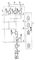
図1は、本発明の実施形態1の固体撮像装置の概略構成を示すブロック図である。図1において、101はMOS型固体撮像素子を備えた画素102がたとえば3行×3列の2次元的に並列されてなる撮像領域、103は撮像領域101内の画素行選択のための垂直走査回路、105は垂直走査回路103に対してスタートパルスを順次供給する制御部、112は垂直走査回路103に対して供給する各種信号を生成する第1〜第3生成手段である生成部、111は垂直走査回路103から各画素行に対して供給される信号を伝送する供給線、108は撮像領域101内の画素列選択のための水平走査回路、109は水平走査回路108によって選択された画素列から読み出された画像信号を順次電圧変換する電圧変換回路、110は電圧変換された画像信号を増幅するアンプである。
【0018】
また、垂直走査回路103は、複数のレジスタ104を有するシフトレジスタと、各レジスタ104の出力に応じて2値の「0」と「1」との状態を維持するカウンタ106と、各カウンタ106の出力に基づいて各画素102に対して読み出し動作またはリセット動作を行う選択行駆動部107とを備えている。ちなみに、垂直走査回路103と水平走査回路108とによって選択手段を構成している。
【0019】
なお、図1及び以下説明する図2,図3において各配線に添えてカッコ書きで付している数字は、後に用いる図4,図5のタイミング図における各信号を識別するものである。
【0020】
図2は、図1の選択行駆動部107及びその周辺の模式的な回路構成図である。選択行駆動部107は、カウンタ106の出力信号と,リセットパルスと転送パルスとを識別するためのパルス信号Prtとを論理合成するイクスクルーシブ・ノア(Exclusive NOR :以下、「EXNOR」と称する。)回路301と、レジスタ104の出力信号とEXNOR回路104の出力信号との論理積を算出する第1論理積回路である論理積(以下、「AND」と称する。)回路302と、AND回路302の出力信号と生成部112で生成されたリセットパルスとの論理積を算出する第2論理積回路であるAND回路303と、AND回路302の出力信号と生成部112で生成された転送パルスとの論理積を算出する第4論理積回路であるAND回路304と、AND回路302の出力信号と生成部112で生成された選択パルスとの論理積を算出する第3論理積回路であるAND回路305とを備えている。
【0021】
なお、AND回路303〜305からの各出力信号の出力線206〜208は、図1の供給線111に相当する。
【0022】
図3は、図1の画素102の模式的な回路構成図である。図2において、201は光電荷を生成するための光電変換素子であるところのフォトダイオード部、202は出力線207を通じて伝送される転送パルスに従ってフォトダイオード部201で生成された光電荷の転送を制御する光電荷転送用MOSトランジスタ、210は転送用MOSトランジスタ202の制御に応じて光電荷が転送される転送領域、203は転送された光電荷に従って増幅してなる画像信号を生成するための増幅用MOSトランジスタ、204は出力線206を通じて伝送されるリセットパルスに従ってフォトダイオード部201及び転送領域210の各電位をリセットするリセット用MOSトランジスタ、205は出力線208を通じて伝送される選択パルスに従って画像信号の読み出しが制御される選択用MOSトランジスタ、209は画像信号が読み出される信号線である。
【0023】
「動作の説明」
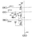
図4,図5は、図1〜図3の動作を説明するタイミング図であり、共に任意の画素行に配置されている画素102の電位をリセットし、その後、光電荷を読み出す動作を行う際に各信号線を伝送する信号を図示しているが、図4には光電荷の蓄積時間を短くする場合のタイミング図であり、図5には光電荷の蓄積時間を長くする場合のタイミング図である。
【0024】
最初に、図4における動作について説明する。まず、制御部105からパルス幅の広い1つのスタートパルスVST及び駆動パルスPVが垂直走査回路103側へ出力される(図4(1),(2))。垂直走査回路103側では、これらのパルスが、順次レジスタ104に入力される。すると、レジスタ104は、スタートパルスVSTがハイレベルの間に、駆動パルスPVに同期した信号を出力する(図4(3))。
【0025】
なお、上記の一連の動作時には、カウンタ106は、「0」を出力しており(図4(4))、また、生成部112ではハイレベル/ローレベルを切り替えたパルス信号Prt、リセットパルスRES、転送パルスTX、選択パルスSELを垂直走査回路103側へそれぞれ出力している(図4(8)〜(10))。
【0026】
ちなみに、図4(5),(8)に示すように、パルス信号Prtは、リセットパルスRESの立ち上がりに同期した信号であり、リセットパルスと転送パルスとを識別するための信号である。
【0027】
つぎに、カウンタ106は、レジスタ104からの出力信号を入力し、その信号の立ち上がりに従って、「0/1」を切り替えた信号を選択行駆動部107側に対して出力する(図4(4))。ここでは、カウンタ106は、「0」を「1」に切り替える。選択行駆動部107側では、この信号が、EXNOR回路301に入力される。また、EXNOR回路301には、カウンタ106からの出力信号の他に、パルス信号Prt(図4(5))が入力され、これらの信号に基づいて算出した信号がAND回路302に対して出力される(図4(6))。
【0028】
AND回路302は、EXNOR回路301からの出力信号(図4(6))とレジスタ104からの出力信号(図4(3))とを入力し、これらの信号に基づいて算出した論理積をAND回路303〜305に対して出力する。AND回路303〜305は、生成部112で生成されたリセットパルスRES、転送パルスTX、選択パルスSEL(図4(8)〜(10))とAND回路302からの出力信号とを入力し、これらの信号に基づいて算出した論理積を出力線206〜208を通じて画素領域101側へ出力する(図4(11)〜(13))。
【0029】
すなわち、図2に示すように構成した垂直走査回路103に、制御部105から図4(1)に示すようなスタートパルスVSTを供給すると、画素領域101には、まず、リセットパルスと転送パルスとが同期してハイレベルで出力され、つづいて転送パルスと選択パルスとが同期してハイレベルで出力される(図4(11)〜(13))。
【0030】
この際、図3に示す画素102では、まずフォトダイオード部201及び転送領域210がリセット電位VDDにリセットされ、つづいて、ほぼ1クロック分の光電荷の蓄積後に、フォトダイオード部201で生成された光電荷に基づく画像信号が読み出し線209に読み出される。
【0031】
次に、図5における動作についての説明であるが、図1〜図3に示した固体撮像装置の構成が変わるわけではないので、図5における動作は、基本的に図4と同様である。但し、以下説明するように、制御部105からは、パルス幅の狭い2つのスタートパルスVSTが出力され、これに応じて結果的に光電荷の蓄積時間が変わる。
【0032】
具体的には、まずスタートパルスVSTがハイレベルの間に、駆動パルスPVに同期した信号を出力するので、レジスタ104の出力信号の波形が異なる(図4(3)、図5(3))。レジスタ104の出力信号の波形が異なると、係る信号とパルス信号Prtとに基づく信号を算出するEXNOR回路301から出力される信号の波形が異なり(図4(6)、図5(6))、したがって、EXNOR回路301から出力される信号の波形に出力波形が依存するAND回路302の出力信号の波形が異なる(図4(7)、図5(7))。
【0033】
AND回路302の出力信号の波形が異なると、この信号波形に依存するAND回路206〜208の出力波形が異なり(図4(11)〜(13)、図5(11)〜(13))、結局、光電荷の蓄積時間を長短が変化する。なお、図5には、水平走査期間の2倍の時間が光電荷の蓄積時間となるようにしているが、たとえば図5(1)、(2)でいうところの駆動パルスPVの3番目のハイレベル時にスタートパルスVSTをハイレベルしているのに代えて、駆動パルスPVの4番目のハイレベル時にスタートパルスVSTをハイレベルにすれば、水平走査期間の3倍の時間が光電荷の蓄積時間となるようにすることができるので、光電荷の蓄積時間は、必要に応じてスタートパルスVSTのハイレベルへの立ち上げ時期を変えることによって制御すればよい。
【0034】
(実施形態2)
図6は、本発明の実施形態2の固体撮像装置の動作を説明するタイミング図であり、図4と同じ光電荷の蓄積時間を実現する際の各種信号のタイミングを示している。また、図6と図5とを比較すると、スタートパルスVSTに関しては、2つのハイレベル期間のローレベルの時間が異なる。
【0035】
すなわち、図6では、連続してスタートパルスVSTを連続してハイレベルにしているのに対して、図4ではスタートパルスVSTを一度ハイレベルにした後に、少し間隔を置いてからスタートパルスVSTをもう一度ハイレベルにしている。本実施形態では、1つ目のスタートパルスVSTと2つ目のスタートパルスVSTとの時間を変えることによって、光電荷の蓄積時間を変えている。
【0036】
(実施形態3)
図7は、実施形態1,2において説明した固体撮像装置を用いた固体撮像システムの構成図である。図7において、1はレンズのプロテクトとメインスイッチを兼ねるバリア、2は被写体の光学像を固体撮像素子4に結像させるレンズ、3はレンズを通った光量を可変するための絞り、4はレンズ2で結像された被写体を画像信号として取り込むための固体撮像素子(上記の各実施形態で説明した固体撮像装置に相当する)、5は固体撮像素子4から出力される画像信号に各種の補正、クランプ等の処理を行う撮像信号処理回路、6は固体撮像素子4より出力される画像信号のアナログ−ディジタル変換を行うA/D変換器、7はA/D変換器6より出力された画像データに各種の補正を行ったりデータを圧縮する信号処理部、8は固体撮像素子4,撮像信号処理回路5,A/D変換器6,信号処理部7に各種タイミング信号を出力するタイミング発生部、9は各種演算とスチルビデオカメラ全体を制御する全体制御・演算部、10は画像データを一時的に記憶するためのメモリ部、11は記録媒体に記録又は読み出しを行うための記録媒体制御インターフェース部、12は画像データの記録又は読み出しを行うための半導体メモリ等の着脱可能な記録媒体、13は外部コンピュータ等と通信するための外部インターフェース(I/F)部である。
【0037】
次に、図7の動作について説明する。バリア1がオープンされるとメイン電源がオンされ、次にコントロール系の電源がオンし、さらに、A/D変換器6などの撮像系回路の電源がオンされる。それから、露光量を制御するために、全体制御・演算部9は絞り3を開放にし、固体撮像素子4から出力された信号は、撮像信号処理回路5をスルーしてA/D変換器6へ出力される。A/D変換器6は、その信号をA/D変換して、信号処理部7に出力する。信号処理部7は、そのデータを基に露出の演算を全体制御・演算部9で行う。
【0038】
この測光を行った結果により明るさを判断し、その結果に応じて全体制御・演算部9は絞りを制御する。次に、固体撮像素子4から出力された信号をもとに、高周波成分を取り出し被写体までの距離の演算を全体制御・演算部9で行う。その後、レンズを駆動して合焦か否かを判断し、合焦していないと判断したときは、再びレンズを駆動し測距を行う。
【0039】
そして、合焦が確認された後に本露光が始まる。露光が終了すると、固体撮像素子4から出力された画像信号は、撮像信号処理回路5において補正等がされ、さらにA/D変換器6でA/D変換され、信号処理部7を通り全体制御・演算9によりメモリ部10に蓄積される。その後、メモリ部10に蓄積されたデータは、全体制御・演算部9の制御により記録媒体制御I/F部を通り半導体メモリ等の着脱可能な記録媒体12に記録される。また外部I/F部13を通り直接コンピュータ等に入力して画像の加工を行ってもよい。
【0040】
【発明の効果】
以上説明したように、本発明によると、スタート信号の入力数やたとえば2つのスタート信号を入力する間の時間を変えることによって、画素のリセットから読み出しまでの時間を変えることができるので、低消費電力を図り、かつ、高速の電子シャッタを実現することができる。
【図面の簡単な説明】
【図1】本発明の実施形態1の固体撮像装置の概略構成を示すブロック図である。
【図2】図1の選択行駆動部及びその周辺の模式的な回路構成図である。
【図3】図1の画素の模式的な回路構成図である。
【図4】図1〜図3の動作を説明するタイミング図である。
【図5】図1〜図3の動作を説明するタイミング図である。
【図6】図1〜図3の動作を説明するタイミング図である。
【図7】実施形態1,2において説明した固体撮像装置を用いた固体撮像システムの構成図である。
【符号の説明】
1 バリア
2 レンズ
3 絞り
4 固体撮像素子
5 撮像信号処理回路
6 A/D変換器
7 信号処理部
8 タイミング発生部
9 全体制御・演算部
10 メモリ部
11 記録媒体制御インターフェース(I/F)部
12 記録媒体
13 外部インターフェース(I/F)部
101 撮像領域
102 画素
103 垂直走査回路
104 レジスタ
105 制御部
106 カウンタ
107 選択行駆動部
108 水平走査回路
109 電圧変換回路
110 アンプ
111 共通線
112 生成部
201 フォトダイオード部
202 転送用MOSトランジスタ
203 増幅用MOSトランジスタ
204 リセット用MOSトランジスタ
205 選択用MOSトランジスタ
206〜208 出力線
209 読み出し線
301 EXNOR回路
302〜305 AND回路[0001]
BACKGROUND OF THE INVENTION
The present invention relates to a solid-state imaging device and system, and more particularly, to a solid-state imaging device and system such as a digital camera, a video camera, a copying machine, and a facsimile.
[0002]
[Prior art]
2. Description of the Related Art Conventionally, there are solid-state imaging devices such as digital cameras, video cameras, copying machines, and facsimiles equipped with an image sensor in which solid-state imaging elements including photoelectric conversion elements are arranged one-dimensionally or two-dimensionally.
[0003]
Solid-state image sensors include, for example, CCD image sensors and MOS image sensors. MOS type image pickup devices are of a type that amplifies signals based on incident light, and among them, a CMOS (complimentary) that can be manufactured using a process having good consistency with a step of forming a metal oxide semiconductor (MOS) transistor. MOS) type sensors.
[0004]
One of the methods for controlling the light accumulation time of the solid-state imaging device is a so-called electronic shutter function. This function adjusts the charge accumulation time of the image pickup unit by driving it, and controls the exposure time electronically instead of the physical aperture function. In order to realize a digital camera that does not have a mechanical shutter and an aperture and to reduce the cost, a high-speed electronic shutter mechanism (up to 1 / 10,000 second) that can shoot even under strong light is required.
[0005]
Specifically, the electronic shutter function is realized by resetting the signal charge accumulated in each solid-state imaging device at a predetermined timing different from pixel signal readout. In other words, in order to realize the electronic shutter function in the solid-state imaging device, the peripheral circuit unit is configured so that the imaging unit can be accessed for reset at a timing different from the access for reading the pixel signal. There is a need to.
[0006]
(Prior art 1)
For this reason, in the conventional solid-state imaging device, as described in, for example, Japanese Patent Application Laid-Open No. H5-227489 or Japanese Patent Application Laid-Open No. H9-93498, an electronic device is provided separately from the row selection shift register for reading image signals. An electronic shutter function has been realized by separately providing a row selection shift register for the shutter function and thereby performing access for resetting the imaging unit.
[0007]
(Prior art 2)
Japanese Patent Application Laid-Open No. 11-220663 discloses a solid-state imaging device using a shift register that realizes both an image signal readout and an electronic shutter function. The method described in this publication includes a selection circuit that selects when the imaging unit is reset and when it is read out. The selection circuit can be accessed from the shift register at different timings by supplying a start pulse having a different pulse width to the shift register when the imaging unit is reset and when reading.
[0008]
Specifically, the output of the register before and after the register corresponding to the actually selected row in the shift register is extracted when the start pulse is input for one column and when the start pulse is input for two columns. This is determined by a logic circuit such as a 3-input NOR circuit.
[0009]
[Problems to be solved by the invention]
However, since the
[0010]
Further, in the
[0011]
That is, the
[0012]
Accordingly, an object of the present invention is to realize a high-speed electronic shutter with low power consumption.
[0013]
[Means for Solving the Problems]
In order to solve the above-described problems, the present invention provides pixels including photoelectric conversion elements arranged in a matrix, signal lines from which signals from a plurality of the pixels are read, and the photoelectric conversion elements for each pixel row. A scanning circuit that selectively performs a reset operation for resetting the signal of the signal and a read operation for reading the signal of the photoelectric conversion element to the output line, and a first generation unit that generates a reset pulse for the reset operation, , and a second generating unit that generates a read pulse for the read operation, the scanning circuit comprises a shift register, one of the first, each of the signals generated by the second generating means in the solid-state imaging device including a selection means for selecting and outputting, and a control unit for supplying a start pulse to said shift register, said selection means, said from the control unit Shifutore Depending on the number of inputs of the start pulse input to the static, in the same pixel row, from the output of the reset pulse generated by said first generating means, to the output of the read pulses generated by the second generating means characterized Rukoto changing the time.
[0014]
In addition, the present invention provides a pixel including photoelectric conversion elements arranged in a matrix, a signal line from which signals from the plurality of pixels are read, and a reset for resetting the signal of the photoelectric conversion element for each pixel row A scanning circuit that selectively performs an operation and a read operation for reading a signal of the photoelectric conversion element to the output line, first generation means for generating a reset pulse for the reset operation, and for the read operation and a second generating unit that generates a read pulse, and said scanning circuit includes a shift register, said first, selecting which selects and outputs one of the signals generated by the second generating means in the solid-state imaging device including a unit, and a control unit for supplying a start pulse to said shift register, said selection means, second start from the first start pulse is input No. In response to the time until the input, in the same pixel row, from the output of the reset pulse generated by said first generating means, to the output of the read pulses generated by the second generating means time changing the characterized Rukoto.
[0015]
Furthermore, a solid-state imaging system of the present invention includes the above-described solid-state imaging device, an optical system that focuses light on the solid-state imaging device, and a signal processing circuit that processes an output signal from the solid-state imaging device. Features.
[0016]
DETAILED DESCRIPTION OF THE INVENTION
Hereinafter, embodiments of the present invention will be described with reference to the drawings.
[0017]
(Embodiment 1)
"Configuration Description"
FIG. 1 is a block diagram showing a schematic configuration of a solid-state imaging device according to
[0018]
The
[0019]
In FIG. 1 and FIGS. 2 and 3 to be described below, numbers in parentheses attached to each wiring identify each signal in the timing diagrams of FIGS. 4 and 5 to be used later.
[0020]
FIG. 2 is a schematic circuit configuration diagram of the selected
[0021]
The
[0022]
FIG. 3 is a schematic circuit configuration diagram of the
[0023]
"Description of operation"
FIGS. 4 and 5 are timing charts for explaining the operations of FIGS. 1 to 3, both of which reset the potential of the
[0024]
First, the operation in FIG. 4 will be described. First, one wide start pulse VST and drive pulse PV are output from the
[0025]
Note that, during the series of operations described above, the
[0026]
Incidentally, as shown in FIGS. 4 (5) and 4 (8), the pulse signal Prt is a signal synchronized with the rising edge of the reset pulse RES, and is a signal for identifying the reset pulse and the transfer pulse.
[0027]
Next, the
[0028]
The AND
[0029]
That is, when the start pulse VST as shown in FIG. 4A is supplied from the
[0030]
At this time, in the
[0031]
Next, the operation in FIG. 5 will be described. Since the configuration of the solid-state imaging device shown in FIGS. 1 to 3 is not changed, the operation in FIG. 5 is basically the same as that in FIG. However, as will be described below, the
[0032]
Specifically, first, since the signal synchronized with the drive pulse PV is output while the start pulse VST is at the high level, the waveform of the output signal of the
[0033]
When the waveform of the output signal of the AND
[0034]
(Embodiment 2)
FIG. 6 is a timing diagram for explaining the operation of the solid-state imaging device according to the second embodiment of the present invention, and shows the timing of various signals when realizing the same photocharge accumulation time as in FIG. Further, comparing FIG. 6 with FIG. 5, regarding the start pulse VST, the low level times of the two high level periods are different.
[0035]
That is, in FIG. 6, the start pulse VST is continuously set to the high level, whereas in FIG. 4, after the start pulse VST is once set to the high level, the start pulse VST is set after a short interval. High level again. In the present embodiment, the photocharge accumulation time is changed by changing the time between the first start pulse VST and the second start pulse VST.
[0036]
(Embodiment 3)
FIG. 7 is a configuration diagram of a solid-state imaging system using the solid-state imaging device described in the first and second embodiments. In FIG. 7, 1 is a barrier that serves as a lens switch and a main switch, 2 is a lens that forms an optical image of a subject on the solid-
[0037]
Next, the operation of FIG. 7 will be described. When the
[0038]
The brightness is determined based on the result of the photometry, and the overall control /
[0039]
Then, after the in-focus state is confirmed, the main exposure starts. When the exposure is completed, the image signal output from the solid-
[0040]
【The invention's effect】
As described above, according to the present invention, it is possible to change the time from pixel reset to readout by changing the number of input start signals and, for example, the time between the input of two start signals. Power can be achieved and a high-speed electronic shutter can be realized.
[Brief description of the drawings]
FIG. 1 is a block diagram illustrating a schematic configuration of a solid-state imaging apparatus according to a first embodiment of the present invention.
2 is a schematic circuit configuration diagram of a selected row driving unit in FIG. 1 and its periphery. FIG.
3 is a schematic circuit configuration diagram of the pixel in FIG. 1. FIG.
FIG. 4 is a timing chart for explaining the operation of FIGS. 1 to 3;
FIG. 5 is a timing chart for explaining the operation of FIGS. 1 to 3;
FIG. 6 is a timing chart for explaining the operation of FIGS. 1 to 3;
FIG. 7 is a configuration diagram of a solid-state imaging system using the solid-state imaging device described in the first and second embodiments.
[Explanation of symbols]
DESCRIPTION OF
Claims (12)
複数の前記画素からの信号が読み出される信号線と、
画素行ごとに、前記光電変換素子の信号をリセットするリセット動作と、前記光電変換素子の信号を前記出力線へ読み出す読み出し動作と、を選択して行う走査回路と、
前記リセット動作のためのリセットパルスを生成する第1生成手段と、
前記読み出し動作のための読み出しパルスを生成する第2生成手段と、を有し、
前記走査回路は、
シフトレジスタと、
前記第1,第2生成手段によって生成された各信号のいずれかを選択して出力する選択手段と、を備えた固体撮像装置において、
前記シフトレジスタにスタートパルスを供給する制御部を有し、
前記選択手段は、前記制御部から前記シフトレジスタに入力されるスタートパルスの入力数に応じて、同一画素行における、前記第1生成手段によって生成されたリセットパルスを出力してから、第2生成手段によって生成された読み出しパルスを出力するまでの時間を変化させることを特徴とする固体撮像装置。 Pixels including photoelectric conversion elements arranged in a matrix;
A signal line from which signals from a plurality of the pixels are read out;
A scanning circuit that selectively performs a reset operation for resetting the signal of the photoelectric conversion element and a read operation for reading out the signal of the photoelectric conversion element to the output line for each pixel row;
First generation means for generating a reset pulse for the reset operation ;
And a second generating unit that generates a read pulse for the read operation,
The scanning circuit includes:
A shift register;
In the solid-state imaging device provided with a selection means for selecting and outputting one of the signals generated by said first, second generation means,
A control unit for supplying a start pulse to the shift register;
The selection unit outputs a reset pulse generated by the first generation unit in the same pixel row in accordance with the number of start pulses input from the control unit to the shift register, and then generates a second generation. a solid-state imaging device according to claim Rukoto changing the time until outputting the read pulses generated by the means.
前記選択手段は、前記第1,第2,第3生成手段で生成された各パルスのいずれかを選択して出力することを特徴とする請求項1から3のいずれか1項記載の固体撮像装置。Further, the pixel comprises a third generation means that generates a transfer pulse light charge generated by the photoelectric conversion element has a transfer area to be transferred, and transfers the charges of the photoelectric conversion element to the transfer region ,
It said selection means, said first, second, third solid-state imaging according to any one of claims 1 to 3, by selecting one of the generated by the generating means pulse and outputs apparatus.
複数の前記画素からの信号が読み出される信号線と、A signal line from which signals from a plurality of the pixels are read out;
画素行ごとに、前記光電変換素子の信号をリセットするリセット動作と、前記光電変換素子の信号を前記出力線へ読み出す読み出し動作と、を選択して行う走査回路と、A scanning circuit that selectively performs a reset operation for resetting the signal of the photoelectric conversion element and a read operation for reading out the signal of the photoelectric conversion element to the output line for each pixel row;
前記リセット動作のためのリセットパルスを生成する第1生成手段と、First generation means for generating a reset pulse for the reset operation;
前記読み出し動作のための読み出しパルスを生成する第2生成手段と、を有し、Second generation means for generating a read pulse for the read operation,
前記走査回路は、The scanning circuit includes:
シフトレジスタと、A shift register;
前記第1,第2生成手段によって生成された各信号のいずれかを選択して出力する選択手段と、を備えた固体撮像装置において、A solid-state imaging device comprising: selection means for selecting and outputting any of the signals generated by the first and second generation means;
前記シフトレジスタにスタートパルスを供給する制御部を有し、A control unit for supplying a start pulse to the shift register;
前記選択手段は、第1スタートパルスが入力されてから第2スタートパルスが入力されるまでの時間に応じて、同一画素行における、前記第1生成手段によって生成されたリセットパルスを出力してから、第2生成手段によって生成された読み出しパルスを出力するまでの時間を変化させることを特徴とする固体撮像装置。The selection unit outputs a reset pulse generated by the first generation unit in the same pixel row according to a time from when the first start pulse is input to when the second start pulse is input. A solid-state imaging device characterized in that the time until the readout pulse generated by the second generation means is output is changed.
前記選択手段は、前記第1,第2,第3生成手段で生成された各パルスのいずれかを選択して出力することを特徴とする請求項6から8のいずれか1項記載の固体撮像装置。9. The solid-state imaging according to claim 6, wherein the selection unit selects and outputs one of the pulses generated by the first, second, and third generation units. apparatus.
前記固体撮像装置へ光を結像する光学系と、
前記固体撮像装置からの出力信号を処理する信号処理回路とを有することを特徴とする固体撮像システム。A solid-state imaging device according to any one of claims 1 to 11 ,
An optical system for imaging light onto the solid-state imaging device;
And a signal processing circuit for processing an output signal from the solid-state imaging device.
Priority Applications (1)
| Application Number | Priority Date | Filing Date | Title |
|---|---|---|---|
| JP2000387510A JP4401566B2 (en) | 2000-12-20 | 2000-12-20 | Solid-state imaging device and system |
Applications Claiming Priority (1)
| Application Number | Priority Date | Filing Date | Title |
|---|---|---|---|
| JP2000387510A JP4401566B2 (en) | 2000-12-20 | 2000-12-20 | Solid-state imaging device and system |
Publications (3)
| Publication Number | Publication Date |
|---|---|
| JP2002190986A JP2002190986A (en) | 2002-07-05 |
| JP2002190986A5 JP2002190986A5 (en) | 2008-02-07 |
| JP4401566B2 true JP4401566B2 (en) | 2010-01-20 |
Family
ID=18854430
Family Applications (1)
| Application Number | Title | Priority Date | Filing Date |
|---|---|---|---|
| JP2000387510A Expired - Fee Related JP4401566B2 (en) | 2000-12-20 | 2000-12-20 | Solid-state imaging device and system |
Country Status (1)
| Country | Link |
|---|---|
| JP (1) | JP4401566B2 (en) |
Families Citing this family (1)
| Publication number | Priority date | Publication date | Assignee | Title |
|---|---|---|---|---|
| JP4946210B2 (en) * | 2006-06-29 | 2012-06-06 | 株式会社ニコン | Solid-state imaging device and imaging apparatus using the same |
-
2000
- 2000-12-20 JP JP2000387510A patent/JP4401566B2/en not_active Expired - Fee Related
Also Published As
| Publication number | Publication date |
|---|---|
| JP2002190986A (en) | 2002-07-05 |
Similar Documents
| Publication | Publication Date | Title |
|---|---|---|
| US7733401B2 (en) | Image capturing apparatus | |
| US8363137B2 (en) | Image sensing apparatus and imaging system | |
| JP5888914B2 (en) | Imaging apparatus and control method thereof | |
| JP6929403B2 (en) | Image sensor and image sensor | |
| JP5317591B2 (en) | Imaging device | |
| JP2010183195A (en) | Imaging pickup apparatus | |
| JP7473041B2 (en) | Image pickup element and image pickup device | |
| US7116367B2 (en) | Solid-state image pickup apparatus having a reset transistor controlled by an output line | |
| US20050128324A1 (en) | Image sensing apparatus and method of controlling same | |
| CN101931745B (en) | Digital camera apparatus | |
| JP2005269452A (en) | Imaging device and imaging apparatus | |
| JP4298685B2 (en) | Shift register, and solid-state imaging device and camera using the shift register | |
| JP2010062639A (en) | Imaging apparatus | |
| JP2005051282A (en) | Driving device and image pickup apparatus | |
| JP2016058877A (en) | Imaging apparatus and control method thereof | |
| JP2020014195A (en) | Imaging device | |
| JP4401566B2 (en) | Solid-state imaging device and system | |
| JP4019409B2 (en) | Solid-state image sensor | |
| JP2020170923A (en) | Imaging element, control method of the same, and imaging apparatus | |
| JP2006060766A (en) | Imaging apparatus and solid-state imaging device | |
| JP2002135795A (en) | Imaging apparatus | |
| JP4232485B2 (en) | Read address control method and apparatus, semiconductor system, and imaging device | |
| JP2008042573A (en) | Imaging apparatus, its control method, imaging system, and program | |
| JP3658401B2 (en) | Solid-state imaging device and camera using the same | |
| JP2003234964A (en) | Digital camera |
Legal Events
| Date | Code | Title | Description |
|---|---|---|---|
| A521 | Request for written amendment filed |
Free format text: JAPANESE INTERMEDIATE CODE: A523 Effective date: 20071214 |
|
| A621 | Written request for application examination |
Free format text: JAPANESE INTERMEDIATE CODE: A621 Effective date: 20071214 |
|
| RD02 | Notification of acceptance of power of attorney |
Free format text: JAPANESE INTERMEDIATE CODE: A7422 Effective date: 20090407 |
|
| RD05 | Notification of revocation of power of attorney |
Free format text: JAPANESE INTERMEDIATE CODE: A7425 Effective date: 20090427 |
|
| A977 | Report on retrieval |
Free format text: JAPANESE INTERMEDIATE CODE: A971007 Effective date: 20090911 |
|
| TRDD | Decision of grant or rejection written | ||
| A01 | Written decision to grant a patent or to grant a registration (utility model) |
Free format text: JAPANESE INTERMEDIATE CODE: A01 Effective date: 20091020 |
|
| A01 | Written decision to grant a patent or to grant a registration (utility model) |
Free format text: JAPANESE INTERMEDIATE CODE: A01 |
|
| A61 | First payment of annual fees (during grant procedure) |
Free format text: JAPANESE INTERMEDIATE CODE: A61 Effective date: 20091028 |
|
| R150 | Certificate of patent or registration of utility model |
Free format text: JAPANESE INTERMEDIATE CODE: R150 |
|
| FPAY | Renewal fee payment (event date is renewal date of database) |
Free format text: PAYMENT UNTIL: 20121106 Year of fee payment: 3 |
|
| FPAY | Renewal fee payment (event date is renewal date of database) |
Free format text: PAYMENT UNTIL: 20131106 Year of fee payment: 4 |
|
| LAPS | Cancellation because of no payment of annual fees |