JP4387397B2 - Ternary memory circuit - Google Patents
Ternary memory circuit Download PDFInfo
- Publication number
- JP4387397B2 JP4387397B2 JP2006298466A JP2006298466A JP4387397B2 JP 4387397 B2 JP4387397 B2 JP 4387397B2 JP 2006298466 A JP2006298466 A JP 2006298466A JP 2006298466 A JP2006298466 A JP 2006298466A JP 4387397 B2 JP4387397 B2 JP 4387397B2
- Authority
- JP
- Japan
- Prior art keywords
- potential
- level
- circuit
- bit line
- reset
- Prior art date
- Legal status (The legal status is an assumption and is not a legal conclusion. Google has not performed a legal analysis and makes no representation as to the accuracy of the status listed.)
- Expired - Lifetime
Links
Images


Landscapes
- Dram (AREA)
Description
本発明は、3値メモリ回路に係り、低電源電圧下であっても3値に対応する電圧値の差を正確に検出することができるセンスアンプ回路とその周辺回路としての2値と3値との間の変換回路とに関する。 The present invention relates to a ternary memory circuit, and a sense amplifier circuit capable of accurately detecting a difference in voltage value corresponding to a ternary value even under a low power supply voltage, and its binary and ternary values as its peripheral circuit. And a conversion circuit between.
現在普及している大容量の半導体メモリの一つは、メモリセル内に1または0の2値情報を記憶し、その2値情報に対応する電圧値をセンスアンプで検出するダイナミック型のRAMである。このメモリのセルは、1個のトランジスタと1個のキャパシタの2素子で構成されることで大容量を可能にしている。 One of the large-capacity semiconductor memories currently in widespread use is a dynamic RAM that stores binary information of 1 or 0 in a memory cell and detects a voltage value corresponding to the binary information with a sense amplifier. is there. This memory cell is configured by two elements of one transistor and one capacitor, thereby enabling a large capacity.
しかしながら、より大容量化を進める為には、単にこのメモリセルの数を増やすだけでは自ずと限界があり、それを解決する方法として3値の情報をメモリセルに記憶させる方法がある。 However, in order to further increase the capacity, there is a limit to simply increasing the number of memory cells, and there is a method of storing ternary information in the memory cells as a method for solving this.
しかしながら、大容量化と共により低い電源電圧下で動作させることも要求されている。その場合、例えば1.0V程度の低い電源電圧下で3値の情報をメモリセルに記憶させると、3値に対応する電圧値の差が非常に狭くなり、それを検出するセンスアンプはより高感度であることが要求される。 However, it is also required to operate under a lower power supply voltage as the capacity increases. In this case, for example, when ternary information is stored in a memory cell under a low power supply voltage of about 1.0 V, the difference in voltage value corresponding to the ternary value becomes very narrow, and a sense amplifier that detects the difference is higher. Sensitivity is required.
従来のDRAMで使用されているセンスアンプは、フリップ・フロップ型のラッチセンスアンプであり、その2つの入力にビット線に読み出されるHレベルまたはLレベルの電圧とそれらの中間の基準電圧とが入力され、基準電圧とビット線の読み出しレベルの差を検出している。しかしながら、かかるラッチセンスアンプでは、それを構成する4個のトランジスタの閾値や電流駆動能力にアンバランスが存在し、それに伴うオフセット電圧の為に、2入力の電位差は少なくとも100mV程度が必要である。 A sense amplifier used in a conventional DRAM is a flip-flop type latch sense amplifier, and an H level or L level voltage read to a bit line and a reference voltage between them are input to two inputs thereof. The difference between the reference voltage and the read level of the bit line is detected. However, in such a latch sense amplifier, there are imbalances in the threshold values and current drive capabilities of the four transistors that constitute the latch sense amplifier, and the potential difference between the two inputs is required to be at least about 100 mV because of the accompanying offset voltage.
一方、現在の1トランジスタ型のメモリセルによって1.0Vの電源電圧下で3値データを記憶する場合、例えばHレベルが1.0V、M(中間)レベルが0.5V、Lレベルが0Vとすると、ビット線とセルの容量比からビット線に読みだされる電圧は+100mV〜−100mVを3つの領域に分割した領域内に入ることになる。従って、1つの区分はせいぜい70mV程度となり、上記した従来のセンスアンプでは入力オフセット電圧以下の電位差となり動作不良を起こすことがある。 On the other hand, when ternary data is stored in a current one-transistor type memory cell under a power supply voltage of 1.0 V, for example, the H level is 1.0 V, the M (intermediate) level is 0.5 V, and the L level is 0 V. Then, the voltage read to the bit line from the capacity ratio of the bit line and the cell enters the region obtained by dividing +100 mV to −100 mV into three regions. Therefore, one division is at most about 70 mV, and the above-described conventional sense amplifier may cause a potential difference equal to or lower than the input offset voltage, resulting in malfunction.
従って、3値メモリ実現の為には、上記した微小電圧差を有効に検出することができるセンスアンプを提供する必要がある。 Therefore, in order to realize a ternary memory, it is necessary to provide a sense amplifier that can effectively detect the minute voltage difference described above.
また、3値メモリ回路を従来から一般的に使用されている2値データのシステム内で使用しようとする場合には、外部の2値データとメモリ内部の3値データとを変換する必要がある。ところが、かかる2値と3値との間の変換回路は従来からあまり提案されておらず、3値メモリを実現する上で必要な要件である。 Further, when the ternary memory circuit is to be used in a binary data system that has been generally used conventionally, it is necessary to convert the external binary data and the ternary data in the memory. . However, a conversion circuit between such binary and ternary values has not been proposed so far, and is a necessary requirement for realizing a ternary memory.
そこで、本発明の目的は、3値メモリを実現するために必要な高感度のセンスアンプ回路を提供することにある。 Accordingly, an object of the present invention is to provide a highly sensitive sense amplifier circuit necessary for realizing a ternary memory.
また、本発明の他の目的は、3値メモリを実現するために必要な2値と3値の間の変換回路を提供することにある。 Another object of the present invention is to provide a binary-to-ternary conversion circuit necessary for realizing a ternary memory.
上記の目的は、本発明によれば、メモリセルに接続されたビット線の電位を増幅する増幅部と、 該ビット線がリセット電位にされた時に該増幅部で増幅された電位を第一のサンプリングパルスにより第一のキャパシタに蓄積する第一のサンプリング保持部と、該メモリセルによりビット線が読出し電位にされた時に該増幅部で増幅された電位を第二のサンプリングパルスにより第二のキャパシタに蓄積する第二のサンプリング保持部と、該第一及び第二のキャパシタに保持されている電位差を検出してラッチするラッチ回路とを有することを特徴とするセンスアンプ回路を提供することにより達成される。 The object of the present invention is to amplify the potential of the bit line connected to the memory cell according to the present invention, and the potential amplified by the amplifier when the bit line is set to the reset potential. A first sampling holding unit that accumulates in the first capacitor by a sampling pulse; and a potential amplified by the amplifying unit when the bit line is set to a read potential by the memory cell by a second sampling pulse. This is achieved by providing a sense amplifier circuit comprising: a second sampling holding unit that stores data in the first and second capacitors; and a latch circuit that detects and latches the potential difference held in the first and second capacitors. Is done.
かかる構成のセンスアンプ回路であれば、ビット線の電位が増幅部で一旦増幅され、その増幅後の電位差がラッチ回路で検出されるので、微小電位差であっても安定して検出することができる。 In the sense amplifier circuit having such a configuration, the potential of the bit line is once amplified by the amplifying unit, and the potential difference after the amplification is detected by the latch circuit, so that even a minute potential difference can be detected stably. .
更に、上記の目的は、本発明によれば、H,M,Lレベルの3値の電位を記憶するメモリセルと、該メモリセルに接続されるビット線と、前記HレベルとMレベルのメモリセルが読みだされた時のビット線の電位の中間の第1のリセット電位にビット線をリセットする第一のリセット回路と、該ビット線を前記Mレベル近傍の第2のリセット電位にリセットする第二のリセット回路と、前記LレベルとMレベルのメモリセルが読みだされた時のビット線の電位の中間の第3のリセット電位に該ビット線をリセットする第三のリセット回路と、前記Hレベルのメモリセルが読みだされた時を検出する第一のセンスアンプ回路と、前記Lレベルのメモリセルが読みだされた時を検出する第二のセンスアンプ回路と、該第一、第二のセンスアンプ回路の出力に従って再書込み電位を前記ビット線にフィードバックする再書き込み回路とを有し、前記第一のセンスアンプ回路は、ビット線の電位を増幅する増幅部と、該ビット線が第1のリセット電位にされた時に該増幅部で増幅された電位を第一のサンプリングパルスにより第一のキャパシタに蓄積する第一のサンプリング保持部と、該メモリセルによりビット線が読出し電位にされた時に該増幅部で増幅された電位を第二のサンプリングパルスにより第二のキャパシタに蓄積する第二のサンプリング保持部と、該第一及び第二のキャパシタに保持されている電位差を検出してラッチするラッチ回路とを有し前記第二のセンスアンプ回路は、ビット線の電位を増幅する増幅部と、該ビット線が第3のリセット電位にされた時に該増幅部で増幅された電位を第一のサンプリングパルスにより第一のキャパシタに蓄積する第一のサンプリング保持部と、該メモリセルによりビット線が読出し電位にされた時に該増幅部で増幅された電位を第二のサンプリングパルスにより第二のキャパシタに蓄積する第二のサンプリング保持部と、該第一及び第二のキャパシタに保持されている電位差を検出してラッチするラッチ回路とを有することを特徴とする3値メモリ回路を提供することにより達成される。 Further, according to the present invention, there is provided a memory cell for storing three-level potentials of H, M, and L levels, a bit line connected to the memory cell, and a memory of the H level and M level. A first reset circuit for resetting the bit line to a first reset potential intermediate the potential of the bit line when the cell is read; and resetting the bit line to a second reset potential near the M level. A second reset circuit; a third reset circuit for resetting the bit line to a third reset potential intermediate between the potentials of the bit lines when the L-level and M-level memory cells are read; A first sense amplifier circuit for detecting when an H level memory cell is read; a second sense amplifier circuit for detecting when an L level memory cell is read; Second sense amplifier times A rewrite circuit that feeds back a rewrite potential to the bit line according to the output of the first sense amplifier circuit, the first sense amplifier circuit amplifying the potential of the bit line, and the bit line being a first reset potential A first sampling holding unit for storing the potential amplified in the amplifying unit in the first capacitor by a first sampling pulse, and the amplifying unit when the bit line is set to the read potential by the memory cell. A second sampling holding unit that accumulates the potential amplified in the second capacitor by a second sampling pulse, and a latch circuit that detects and latches the potential difference held in the first and second capacitors The second sense amplifier circuit includes an amplifying unit for amplifying the potential of the bit line and an increase in the amplifying unit when the bit line is set to the third reset potential. A first sampling holding unit for storing the generated potential in a first capacitor by a first sampling pulse, and a potential amplified by the amplifying unit when the bit line is set to a read potential by the memory cell. A three-valued circuit comprising: a second sampling holding unit that accumulates in a second capacitor by a sampling pulse; and a latch circuit that detects and latches a potential difference held in the first and second capacitors. This is achieved by providing a memory circuit.
上記の様に、二つのセンスアンプ回路を設けることで、3値情報を記憶するメモリセルの場合でも、安定して検出することができる。 As described above, providing two sense amplifier circuits enables stable detection even in the case of a memory cell storing ternary information.
上記の様な3値情報を記憶するメモリ回路の場合に、センスアンプ回路から出力回路まで又は入力回路から書き込み増幅回路までの3値信号を信号成形する必要がある。 In the case of a memory circuit for storing ternary information as described above, it is necessary to form a ternary signal from the sense amplifier circuit to the output circuit or from the input circuit to the write amplifier circuit.
その成形回路として、本発明では、所定電位の電源に接続され、H,M,Lレベルを有する3値入力をゲートに入力する第一のPチャネルトランジスタと、接地電源に接続され、前記3値入力をゲートに入力する第一のNチャネルトランジスタと、前記第一のPチャネルトランジスタと第一のNチャネルトランジスタの間に設けられ、リセット時に非導通となりリセット時以外で導通となる第二のP,Nチャネルトランジスタと、該第二のP,Nチャネルトランジスタの接続点に接続され、リセット時に前記Mレベルの電位にリセットされる出力端子とを有することを特徴とする3値インバータ回路が提供される。 As the forming circuit, in the present invention, a ternary P-channel transistor connected to a power source of a predetermined potential and inputting a ternary input having H, M, and L levels to the gate and a ground power source is connected to the ternary value. A first N-channel transistor that inputs an input to a gate, and a second P that is provided between the first P-channel transistor and the first N-channel transistor and is non-conductive at reset and conductive at other times than reset. , An N-channel transistor, and an output terminal connected to the connection point of the second P, N-channel transistor and reset to the M-level potential at reset is provided. The
また、本発明によれば、上記の3値インバータ回路において、リセット時の出力端子の電位をHレベルにするかLレベルにするかで、3値信号のHレベル又はLレベル信号を検出することができる。 According to the present invention, in the ternary inverter circuit described above, the H level or L level signal of the ternary signal is detected depending on whether the potential of the output terminal at the time of reset is set to H level or L level. Can do.
上記した目的は、本発明によれば、2進数の3ビット信号を3進数の2ビット信号に変換するデコーダ回路において、該2進数の3ビット信号のうち第一、第二のビット信号が所定の組み合わせの時を検出する例外検出部と、該例外が検出されない時に、該第一、第二のビット信号を入力して反転させ、該例外が検出される時に2進数の3ビット信号のうち第三のビット信号を入力して反転させる第一及び第二のマルチプレクサ回路と、該例外が検出されない時に、該第一及び第二のマルチプレクサ回路からの出力信号を入力し、該第一、第二のビット信号の組み合わせに従って、L,M,Hレベルを3進数の第一のビット信号として出力し、該例外が検出される時に、前記2進数の第三のビット信号を3進数の第一のビット信号として出力する第一のインバータ回路と、該例外が検出されない時に、前記2進数の第三のビット信号に従って、LレベルとMレベルを3進数の第二のビット信号として出力し、前記例外が検出される時に、Hレベルを3進数の第二のビット信号として出力する第二のインバータ回路とを有することを特徴とするデコーダ回路を提供することにより達成される。 According to the present invention, in the decoder circuit for converting a binary 3-bit signal into a binary 2-bit signal, the first and second bit signals of the binary 3-bit signal are predetermined. An exception detection unit that detects when the combination is detected, and when the exception is not detected, the first and second bit signals are input and inverted, and when the exception is detected, of the binary 3-bit signal First and second multiplexer circuits that receive and invert a third bit signal, and when the exception is not detected, input an output signal from the first and second multiplexer circuits, and According to the combination of the two bit signals, the L, M, and H levels are output as a ternary first bit signal, and when the exception is detected, the binary third bit signal is output as the ternary first bit signal. Output as bit signal When the exception is not detected, the L level and the M level are output as a ternary second bit signal according to the binary third bit signal, and the exception is detected. This is achieved by providing a decoder circuit characterized in that it has a second inverter circuit that outputs an H level as a ternary second bit signal.
また、同じ目的は、本発明によれば、3進数の2ビット信号を2進数の3ビット信号に変換するエンコーダ回路において、3進数の第一のビット信号のHレベルを検出する回路とLレベルを検出する回路と、3進数の第二のビット信号のHレベルを検出する回路とLレベルを検出する回路と、上記Hレベル又はLレベル検出回路のいずれかの第一の出力が所定の信号の時に例外時と判定され、該判定信号により制御される第一、第二、第三のマルチプレクサ回路とを有し、該第一のマルチプレクサ回路は、該例外が検出されない時に前記第一の出力に対応する逆相レベルの検出回路の第二の出力を反転し、該例外が検出される時に他方のビット信号のHレベル又はLレベル検出回路の一方の出力を反転し、該第二のマルチプレクサ回路は、該例外が検出されない時に前記他方のビット信号のHレベル又はLレベル検出回路の一方の出力を反転し、該例外が検出される時にH又はLレベルの何れかの一方のレベルを出力し、該第三のマルチプレクサ回路は、該例外が検出されない時に前記他方のビット信号のHレベル又はLレベル検出回路の他方の出力を反転し、該例外が検出される時にH又はLレベルの何れかの他方のレベルを出力することを特徴とするエンコーダ回路。 Another object of the present invention is to provide an encoder circuit for converting a ternary 2-bit signal into a binary 3-bit signal according to the present invention, and a circuit for detecting the H level of the ternary first bit signal and the L level. , A circuit for detecting the H level of the ternary second bit signal, a circuit for detecting the L level, and the first output of either the H level or L level detection circuit is a predetermined signal. And the first, second, and third multiplexer circuits that are determined as an exception time and controlled by the determination signal, and the first multiplexer circuit includes the first output when the exception is not detected. The second output of the detection circuit corresponding to the opposite phase level is inverted, and when the exception is detected, the output of one of the H level or L level detection circuit of the other bit signal is inverted, and the second multiplexer The circuit When the outside is not detected, the output of one of the H level and L level detection circuits of the other bit signal is inverted, and when the exception is detected, one level of either H or L level is output, The third multiplexer circuit inverts the other output of the H level or L level detection circuit of the other bit signal when the exception is not detected, and the other of either the H level or the L level when the exception is detected. An encoder circuit that outputs a level.
以下,図面にしたがって本発明の実施の形態について説明する。但し,本発明の技術的範囲はこれらの実施の形態に限定されず,特許請求の範囲に記載された事項とその均等物まで及ぶものである。 Hereinafter, embodiments of the present invention will be described with reference to the drawings. However, the technical scope of the present invention is not limited to these embodiments, but extends to the matters described in the claims and equivalents thereof.
以下、本発明の実施の形態について図面に従って説明する。しかしながら、本発明の技術的範囲がかかる実施の形態に限定されるものではない。 Hereinafter, embodiments of the present invention will be described with reference to the drawings. However, the technical scope of the present invention is not limited to such an embodiment.
[センスアンプの動作原理]
図1は、本発明にかかるセンスアンプの動作原理を説明する為の回路図であり、図2はその動作原理を説明する為のタイミングチャート図である。本明細書では、Pチャネル型MOSトランジスタについてはPを引用符号として使用し、Nチャネル型MOSトランジスタについてはQを引用符号として使用する。
[Operation principle of sense amplifier]
FIG. 1 is a circuit diagram for explaining the operation principle of the sense amplifier according to the present invention, and FIG. 2 is a timing chart for explaining the operation principle. In this specification, P is used as a reference symbol for a P-channel MOS transistor, and Q is used as a reference symbol for an N-channel MOS transistor.
図1の回路内のNチャネル型MOSトランジスタは閾値電圧が0.6Vで、Pチャネル型MOSトランジスタは閾値電圧が−0.6Vであるとする。図1の回路は、メモリセルMC、リセット回路RST及びセンスアンプSAから構成される。メモリセルMCは、ビット線BLとワード線WORDとの交差部に設けられたトランジスタQ3とキャパシタCcから構成されている。キャパシタCcの対向電極は電源の中間電位である0.5Vが印加されている。また、リセット回路RSTは、ビット線BLの電位を0.5Vの基準電位VREFにリセットする回路である。 The threshold voltage of the N-channel MOS transistor in the circuit of FIG. 1 is 0.6V, and the threshold voltage of the P-channel MOS transistor is −0.6V. The circuit in FIG. 1 includes a memory cell MC, a reset circuit RST, and a sense amplifier SA. The memory cell MC includes a transistor Q3 and a capacitor Cc provided at the intersection between the bit line BL and the word line WORD. The counter electrode of the capacitor Cc is applied with 0.5 V which is an intermediate potential of the power source. The reset circuit RST is a circuit that resets the potential of the bit line BL to a reference potential VREF of 0.5V.
図1のセンスアンプSAには、ビット線BLの電位を増幅するP型トランジスタP1と定電流源のN型トランジスタQ1からなる増幅回路が設けられ、電源電圧を昇圧した1.5V電位に接続されている。更に、基準電圧VREFを増幅した時のノードnampをサンプリング保持する回路P2,C1と、読み出した時のビット線電位を増幅した時のノードnampをサンプリング保持する回路P3,C2と、それぞれの保持電位であるノードn1,n2の電位差を検出するラッチ回路Q4,Q5,Q6を有する。 The sense amplifier SA of FIG. 1 is provided with an amplifier circuit composed of a P-type transistor P1 for amplifying the potential of the bit line BL and an N-type transistor Q1 as a constant current source, and is connected to a 1.5 V potential obtained by boosting the power supply voltage. ing. Further, circuits P2 and C1 for sampling and holding the node namp when the reference voltage VREF is amplified, circuits P3 and C2 for sampling and holding the node namp when the bit line potential at the time of reading is amplified, and respective holding potentials Latch circuits Q4, Q5, Q6 for detecting a potential difference between nodes n1, n2.
次に、図2に示したタイミングチャート図に従って図1の動作の説明を行なう。ここでは、動作原理の説明であるため、メモリセルMCのノードnceには、Hレベルの1VとLレベルの0Vとが蓄積されているとする。先ず、期間t1においてリセットパルスφRSTが1.5Vに立ち上がりビット線BLを基準電位VREFレベルにリセットする。そのビット線電位は増幅トランジスタP1により増幅され、ノードnampに基準電位VREFに対応した電位が生成され、サンプルパルスφ1のLレベルによりトランジスタP2を介してその電位がキャパシタC1にサンプルされる。 Next, the operation of FIG. 1 will be described with reference to the timing chart shown in FIG. Here, since it is an explanation of the operation principle, it is assumed that 1V of H level and 0V of L level are stored in the node nce of the memory cell MC. First, in the period t1, the reset pulse φRST rises to 1.5V, and the bit line BL is reset to the reference potential VREF level. The bit line potential is amplified by the amplification transistor P1, a potential corresponding to the reference potential VREF is generated at the node namp, and the potential is sampled to the capacitor C1 via the transistor P2 by the L level of the sample pulse φ1.
上記のリセット期間の後、ワード線WORDが1.5Vに立ち上げられ、メモリセルに蓄積されていたHレベルに対応する電荷がビット線BLに流れだす。ビット線の容量負荷をCBLとすると、ビット線BLの電位は、VREF+Cc/(CBL+Cc)×0.5V(通常、Cc/(CBL+Cc)は0.1程度)
に上昇する。その上昇分の約0.05Vが、増幅トランジスタP1により増幅され、ノードnampの電位はより低くなる。そして、期間t2において、サンプルパルスφ2のLレベルによりトランジスタP3を介してその電位がキャパシタC2にサンプルされる。
After the reset period, the word line WORD is raised to 1.5V, and the charge corresponding to the H level stored in the memory cell flows out to the bit line BL. When the capacity load of the bit line is CBL, the potential of the bit line BL is VREF + Cc / (CBL + Cc) × 0.5 V (normally, Cc / (CBL + Cc) is about 0.1)
To rise. About 0.05 V of the increase is amplified by the amplification transistor P1, and the potential of the node namp becomes lower. In the period t2, the potential is sampled in the capacitor C2 through the transistor P3 by the L level of the sample pulse φ2.
その後、期間t3において、ラッチパルスφLATCH によってラッチ回路が活性化され、サンプリングされていたノードn1とn2の電位差が検出される。 Thereafter, in the period t3, the latch circuit is activated by the latch pulse φLATCH, and the potential difference between the nodes n1 and n2 that have been sampled is detected.
期間t4,t5,t6においては、メモリセルのLレベルを検出するために、リセット電位のサンプリング、読み出し電位のサンプリング及びラッチ増幅がそれぞれ行なわれる。 In the periods t4, t5, and t6, reset potential sampling, read potential sampling, and latch amplification are performed in order to detect the L level of the memory cell.
上記の通り、ビット線BLに発生する±Cc/(CBL+Cc)×0.5V(約0.05V)の電位変動は、増幅トランジスタP1により増幅され、その増幅後の電位のノードn1とn2がラッチ回路で確実に差動増幅される。具体的には、ビット線BLに生じる±0.05V程度の電圧は、増幅トランジスタP1によって±0.2V程度まで増幅される。 As described above, the potential fluctuation of ± Cc / (CBL + Cc) × 0.5V (about 0.05V) generated in the bit line BL is amplified by the amplification transistor P1, and the nodes n1 and n2 of the potential after the amplification are latched. The circuit is surely differentially amplified. Specifically, a voltage of about ± 0.05 V generated on the bit line BL is amplified to about ± 0.2 V by the amplification transistor P1.
上記説明した通り、図1のセンスアンプ回路では、リセット時のビット線の電位と読み出し時の電位とを時分割でサンプリングしている。しかしながら、サンプルパルスφ1,2のパルス幅を狭くすることにより、メモリの読み出し動作に特に影響を与えることは少ない。即ち、サンプルパルスφ1,2が短いパルスであっても、ノードnapmに生成される増幅された電位に応じてトランジスタP2,P3のゲート・ソース間電圧が異なるので、それに伴いノードnampが高い場合には多くの電流、低い場合には少ない電流がそれぞれ流れるので、結果的にキャパシタC1,C2に充電される電位の差はノードnampの電位差の4〜5倍に増幅された値になる。 As described above, in the sense amplifier circuit of FIG. 1, the bit line potential at the time of reset and the potential at the time of reading are sampled in a time division manner. However, by narrowing the pulse width of the sample pulses φ1 and φ2, the memory read operation is not particularly affected. That is, even when the sample pulses φ1 and φ2 are short pulses, the gate-source voltages of the transistors P2 and P3 differ depending on the amplified potential generated at the node napm. Since a large current flows and a small current flows when the current is low, the difference between the potentials charged in the capacitors C1 and C2 results in a value amplified to 4 to 5 times the potential difference at the node namp.
[3値DRAMへの適用例]
図3は、上記のセンスアンプ回路を3値DRAMに適用した時の回路図である。また、図4はその動作を説明するタイミングチャート図である。この例でも、電源電圧は1V、NMOSトランジスタの閾値は0.6V、PMOSトランジスタの閾値は−0.6Vとする。
[Example of application to ternary DRAM]
FIG. 3 is a circuit diagram when the above-described sense amplifier circuit is applied to a ternary DRAM. FIG. 4 is a timing chart for explaining the operation. Also in this example, the power supply voltage is 1V, the threshold value of the NMOS transistor is 0.6V, and the threshold value of the PMOS transistor is -0.6V.
図示される通り、リセット回路RSTには3種類のリセット電位(0.52V,0.5V,0.48V)が準備されている。そして、メモリセルとして図中にはHレベル(1V)を記憶するメモリセルMCH,Mレベル(0.5V)を記憶するメモリセルMCM,Lレベル(0V)を記憶するメモリセルMCLの3個が示されている。ビット線BLに接続されるセンスアンプ回路SAには、図1で説明したセンスアンプ回路が2組SA1,SA2設けられている。それらのセンスアンプSA1,SA2からの出力が再書き込み回路RWを介して、ビット線BLに戻されている。 As shown in the figure, three types of reset potentials (0.52 V, 0.5 V, 0.48 V) are prepared in the reset circuit RST. In the figure, there are three memory cells, a memory cell MCH that stores H level (1V), a memory cell MCM that stores M level (0.5V), and a memory cell MCL that stores L level (0V). It is shown. The sense amplifier circuit SA connected to the bit line BL is provided with two sets of sense amplifier circuits SA1 and SA2 described in FIG. Outputs from these sense amplifiers SA1 and SA2 are returned to the bit line BL via the rewrite circuit RW.
センスアンプSA1は、ビット線BLが高いリセットレベルVRHにリセットされている時のノードnamp1の電位をキャパシタC11にサンプリングし、メモリセルから読みだされた時のノードnamp1の電位をキャパシタC21にサンプリングする。つまり、ビット線の電位が、Hレベルの値に対応するか否かの判定を行なう。従って、Hレベルが読みだされる時は、ビット線電位はより高く変化し、ノードnamp1はより低く増幅されるので、n11>n21の電位関係となり、ノードn21はLレベルとして読みだされる。Hレベル以外の場合には、n11<n21となる。 The sense amplifier SA1 samples the potential of the node namp1 when the bit line BL is reset to the high reset level VRH into the capacitor C11, and samples the potential of the node namp1 when read from the memory cell into the capacitor C21. . That is, it is determined whether or not the potential of the bit line corresponds to an H level value. Therefore, when the H level is read, the bit line potential changes higher, and the node namp1 is amplified lower. Therefore, the potential relationship is n11> n21, and the node n21 is read as the L level. In cases other than the H level, n11 <n21.
センスアンプSA2は、ビット線BLに低いリセットレベルVRLにリセットされている時のノードnamp2の電位をキャパシタC12にサンプリングし、メモリセルから読みだされた時のノードnamp2の電位をキャパシタC22にサンプリングする。つまり、ビット線の電位が、Lレベルの値に対応するか否かの判定を行なう。従って、Lレベルが読みだされる時は、ビット線電位はより低く変化し、ノードnamp2はより高い電位になるので、n12<n22の電位関係となり、ノードn22はHレベルとして読みだされる。Lレベル以外の場合には、n12>n22となる。 The sense amplifier SA2 samples the potential of the node namp2 when the bit line BL is reset to the low reset level VRL into the capacitor C12, and samples the potential of the node namp2 when read from the memory cell into the capacitor C22. . That is, it is determined whether or not the potential of the bit line corresponds to the L level value. Therefore, when the L level is read, the bit line potential changes lower, and the node namp2 becomes a higher potential. Therefore, the potential relationship of n12 <n22 is established, and the node n22 is read as the H level. In cases other than the L level, n12> n22.
従って、1対のセンスアンプSA1,SA2の出力n21,n22の出力は、Hレベル読み出し時:n21=L,n22=LMレベル読み出し時:n21=H,n22=LLレベル読み出し時:n21=H,n22=Hとなる。 Therefore, the outputs n21 and n22 of the pair of sense amplifiers SA1 and SA2 are H level read: n21 = L, n22 = LM level read: n21 = H, n22 = LL level read: n21 = H, n22 = H.
再書き込み回路は、一対の逆相信号φW,/φWにより活性化され、1組のセンスアンプSA1,SA2で検出された出力によって再書き込み電位(1V,0.5V,0V)をビット線にフィードバックする。 The rewrite circuit is activated by a pair of opposite-phase signals φW and / φW, and a rewrite potential (1V, 0.5V, 0V) is fed back to the bit line by outputs detected by a pair of sense amplifiers SA1 and SA2. To do.
読み出し時のビット線電位が、リセット電位VRHより高い場合は、n21=0V,n22=0Vとなり、トランジスタP24がオン、Q28がオフとなり、再書き込み電位は1Vとなる。 When the bit line potential at the time of reading is higher than the reset potential VRH, n21 = 0V and n22 = 0V, the transistor P24 is turned on, Q28 is turned off, and the rewriting potential is 1V.
読み出し時のビット線電位が、リセット電位VRLより低い場合は、n21=H,n22=Hとなり、トランジスタP24がオフ、Q28がオンとなり、再書き込み電位は0Vとなる。 When the bit line potential at the time of reading is lower than the reset potential VRL, n21 = H, n22 = H, the transistor P24 is turned off, Q28 is turned on, and the rewriting potential is 0V.
読み出し時のビット線電位が、中間値の場合は、n21=H,n22=0Vとなるので、トランジスタP24,Q28が共にオフとなり、ビット線電位がそのまま再書き込みされる。このビット線電位は、読み出し直前に0.5Vにリセットされ、セルへのアクセスにより±0.02V以下の変動をする。しかし、その変動分は、次のアクセス時にCc/(CBL+Cc)倍(約0.1倍)され、ビット線には0.5V±0.002Vが読みだされるので、Mレベルの読み出しに支障はない。 When the bit line potential at the time of reading is an intermediate value, n21 = H and n22 = 0V, so that both the transistors P24 and Q28 are turned off and the bit line potential is rewritten as it is. This bit line potential is reset to 0.5 V immediately before reading, and fluctuates by ± 0.02 V or less due to access to the cell. However, the fluctuation amount is Cc / (CBL + Cc) times (about 0.1 times) at the next access, and 0.5 V ± 0.002 V is read out to the bit line, which hinders reading at the M level. There is no.
尚、ノードn21がHレベルの時にトランジスタP24がオフする為には0.4V(1V−Vth(0.6))以上であることが必要で、ノードn22がHレベルの時にトランジスタQ28がオンする為には0.6V(Vth)以上であることが必要である。センスアンプSA1,2内のラッチ回路にはプルアップ回路がないので、サンプル電圧のnamp1とnamp2の電位が0.6V以上になる様に、増幅回路のトランジスタP11,Q11とP12,Q12のディメンジョン比は若干異なっている。即ち、トランジスタP11,Q11は、ビット線BLがHレベルリセット電位VRHの時にノードnamp1>0.6Vとなるように設定されている。また、トランジスタP12,Q12は、ビット線BLがLレベルリセット電位VRLの時にノードnamp2>0.6Vとなるように設定されている。従って、例えばビット線BLが0.5Vの時は、namp1>namp2となる。 In order to turn off the transistor P24 when the node n21 is at the H level, it is necessary to be 0.4 V (1V-Vth (0.6)) or more. When the node n22 is at the H level, the transistor Q28 is turned on. For this purpose, it is necessary to be 0.6 V (Vth) or more. Since the latch circuits in the sense amplifiers SA1 and SA2 do not have a pull-up circuit, the dimension ratio of the transistors P11, Q11 and P12, Q12 of the amplifier circuit is set so that the potentials of the sample voltages namp1 and namp2 are 0.6V or more Are slightly different. That is, the transistors P11 and Q11 are set so that the node namp1> 0.6V when the bit line BL is at the H level reset potential VRH. The transistors P12 and Q12 are set so that the node namp2> 0.6V when the bit line BL is at the L level reset potential VRL. Therefore, for example, when the bit line BL is 0.5 V, namp1> namp2.
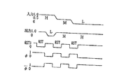
図3の動作を図4のタイミングチャート図に従って説明する。図4は、Hレベル読み出しと再書き込み、Mレベル読み出しと再書き込み、Lレベル読み出しと再書き込みを順に動作している。 The operation of FIG. 3 will be described with reference to the timing chart of FIG. FIG. 4 operates in order of H level reading and rewriting, M level reading and rewriting, L level reading and rewriting.
[Hレベル読み出しと再書き込み]
先ず、リセット期間では、リセット信号φRST1が立ち上がり、ビット線BLをVRL(0.48V)にリセットし、その時のセンスアンプSA2内のノードnamp2がサンプルパルスφ1の立ち下がりによりキャパシタC12にサンプルされる。次にリセット信号φRST2が立ち上がり、ビット線BLをVRH(0.52V)にリセットし、その時のセンスアンプSA1内のノードnamp1がサンプルパルスφ2の立ち下がりによりキャパシタC11にサンプルされる。そして最後に、リセット信号φRST3が立ち上がり、ビット線BLはVRM(0.5V)にリセットされる。
[H level read and rewrite]
First, in the reset period, the reset signal φRST1 rises to reset the bit line BL to VRL (0.48V), and the node namp2 in the sense amplifier SA2 at that time is sampled by the capacitor C12 by the fall of the sample pulse φ1. Next, the reset signal φRST2 rises to reset the bit line BL to VRH (0.52 V), and the node namp1 in the sense amplifier SA1 at that time is sampled by the capacitor C11 by the fall of the sample pulse φ2. Finally, the reset signal φRST3 rises and the bit line BL is reset to VRM (0.5 V).
そこで、ワード線WLHが2.0Vまで立ち上がり、メモリセルMCHの選択トランジスタQ31が導通し、ビット線BLにはCc/(CBL+Cc)×0.5V(約0.05V)の電位増加が発生する。それに従って増幅トランジスタP11,P12によって低下したノードnamp1,2の電位がサンプルパルスφ3でキャパシタC21,C22にサンプリングされる。従って、センスアンプSA1では十分な電位差ΔVをもってn11>n21となり、ラッチパルスφLATCHの立ち下がりにより、ノードn21は0Vまで引き下げられる。その時、センスアンプSA2側のノードn22も0Vまで引き下げられる。従って、ノードn21とn22はいずれもLレベルとなる。 Therefore, the word line WLH rises to 2.0V, the selection transistor Q31 of the memory cell MCH becomes conductive, and a potential increase of Cc / (CBL + Cc) × 0.5V (about 0.05V) occurs in the bit line BL. Accordingly, the potentials of the nodes namp1 and 2 reduced by the amplification transistors P11 and P12 are sampled in the capacitors C21 and C22 by the sample pulse φ3. Accordingly, in the sense amplifier SA1, n11> n21 with a sufficient potential difference ΔV, and the node n21 is pulled down to 0 V by the falling of the latch pulse φLATCH. At that time, the node n22 on the sense amplifier SA2 side is also pulled down to 0V. Therefore, both nodes n21 and n22 are at the L level.
そして、再書き込み回路RWがパルス/φW,φWで活性化されると、トランジスタP24とP25がオンし、1Vの電源電位がビット線BLに戻され、メモリセルMCHのキャパシタCaに再書き込みされる。 When the rewrite circuit RW is activated by the pulses / φW and φW, the transistors P24 and P25 are turned on, the 1V power supply potential is returned to the bit line BL, and the data is rewritten to the capacitor Ca of the memory cell MCH. .
[Mレベル読み出しと再書き込み]
リセット期間は、上記と同様である。そして、ワード線WLMが2.0Vまで立ち上がると、メモリセルMCM内には0.5Vが記憶されているので、ビット線BLの電位は変化なくリセット電位VRM(0.5V)を維持する。その時のノードnamp1,2の電位がキャパシタC21,C22にそれぞれサンプリングされる。従って、n11<n21,n12>n22の状態が、ラッチパルスφLATCH の立ち下がりによりラッチされる。従って、ノードn21はHレベル、n22はLレベルとなる。
[M level read and rewrite]
The reset period is the same as described above. When the word line WLM rises to 2.0V, 0.5V is stored in the memory cell MCM, so that the potential of the bit line BL remains unchanged and the reset potential VRM (0.5V) is maintained. The potentials of the nodes namp1 and namp2 at that time are sampled in the capacitors C21 and C22, respectively. Therefore, the state of n11 <n21, n12> n22 is latched by the falling edge of the latch pulse φLATCH. Therefore, the node n21 is at the H level and n22 is at the L level.
その後、再書き込み回路RWがパルス/φW,φWで活性化されても、トランジスタP24,Q28はオフのままで、ビット線BLの電位はリセット電位の0.5Vのままに維持され、メモリセルMCMに再書き込みされる。 Thereafter, even if the rewrite circuit RW is activated by the pulses / φW and φW, the transistors P24 and Q28 remain off, and the potential of the bit line BL is maintained at the reset potential of 0.5 V, so that the memory cell MCM Will be rewritten.
[Lレベル読み出しと再書き込み]
リセット期間は、上記と同様である。そして、ワード線WLLが2.0Vまで立ち上がると、メモリセルMCL内には0Vが記憶されているので、ビット線BLの電位はCc/(CBL+Cc)×0.5V(約0.05V)の電位低下が発生する。それに従って増幅トランジスタP11,P12によって増加したノードnamp1,2の電位がサンプルパルスφ3でキャパシタC21,C22にサンプリングされる。従って、センスアンプSA2では十分な電位差ΔVをもってn12<n22となり、ラッチパルスφLATCH の立ち下がりにより、ノードn22はHレベルとなる。その時、センスアンプSA1側のノードn21もHレベルになる。従って、ノードn21とn22はいずれもHレベルとなる。
[L level read and rewrite]
The reset period is the same as described above. When the word line WLL rises to 2.0V, 0V is stored in the memory cell MCL, so that the potential of the bit line BL is a potential of Cc / (CBL + Cc) × 0.5V (about 0.05V). A decrease occurs. Accordingly, the potentials of the nodes namp1, 2 increased by the amplification transistors P11, P12 are sampled in the capacitors C21, C22 by the sample pulse φ3. Therefore, in the sense amplifier SA2, n12 <n22 with a sufficient potential difference ΔV, and the node n22 becomes H level by the fall of the latch pulse φLATCH. At that time, the node n21 on the sense amplifier SA1 side is also at the H level. Therefore, both the nodes n21 and n22 are at the H level.
そして、再書き込み回路RWがパルス/φW,φWで活性化されると、トランジスタQ27,Q28がオンし、0Vの電源電位がビット線BLに戻され、メモリセルMCLのキャパシタCcに再書き込みされる。 When the rewrite circuit RW is activated by the pulses / φW and φW, the transistors Q27 and Q28 are turned on, the power supply potential of 0 V is returned to the bit line BL, and rewritten to the capacitor Cc of the memory cell MCL. .
以上の様に、Hレベル検出とLレベル検出をそれぞれ専用に行なうセンスアンプを1組使用することで、1Vの電源電圧下での3値レベルをメモリセルから確実に読みだして再書き込みすることができる。 As described above, by using one set of sense amplifiers dedicated to H level detection and L level detection, the ternary level under a power supply voltage of 1 V can be reliably read from the memory cell and rewritten. Can do.
[3値インバータ等]
上記した様に、再書き込み回路RWの出力には、Hレベル(1V),Mレベル(0.5V),Lレベル(0V)がそれぞれ読みだされる。従って、その出力を図示しない出力回路に供給する必要がある。或いは図示しない入力回路から書き込み回路まで3値信号を供給する必要がある。メモリセルアレイが複数のブロックに分割されている場合などは、その中間で増幅する必要がある。また、出力回路内等で必要に応じて、Hレベルを検出したり、Lレベルを検出したりする回路も適宜利用することが必要になる。そこで、以下に3値インバータ、Hレベル検出回路、Lレベル検出回路の例について説明する。
[Ternary inverter, etc.]
As described above, H level (1 V), M level (0.5 V), and L level (0 V) are read from the output of the rewrite circuit RW. Therefore, it is necessary to supply the output to an output circuit (not shown). Alternatively, it is necessary to supply a ternary signal from an input circuit (not shown) to a writing circuit. When the memory cell array is divided into a plurality of blocks, it is necessary to amplify in the middle. In addition, it is necessary to appropriately use a circuit for detecting the H level or detecting the L level as needed in the output circuit or the like. Therefore, examples of a ternary inverter, an H level detection circuit, and an L level detection circuit will be described below.
図5は、3値インバータ回路例であり、図6はその動作波形図である。この回路は、図3の再書き込み回路と同様の動作を行なう。電源電圧は1V、PチャネルMOS及びNチャネルMOSそれぞれのトランジスタの閾値は0.6Vと−0.6Vである。 FIG. 5 is an example of a ternary inverter circuit, and FIG. 6 is an operation waveform diagram thereof. This circuit performs the same operation as the rewrite circuit of FIG. The power supply voltage is 1V, and the threshold values of the P channel MOS transistor and the N channel MOS transistor are 0.6V and -0.6V, respectively.
図5の回路は、クロックφ,/φで活性化されるインバータP31,P32,Q33,Q34と、リセットトランジスタQ35から構成される。その動作は、リセット時に、クロックφ,/φを1V,0VにしてトランジスタP32,Q33をオフ状態にし、リセット信号RSTを1.5Vに立ち上げて出力端子をMレベルの0.5Vにリセットする。その後、リセット信号RSTを0Vに立ち下げて、クロックφ,/φを0V,1VにしてトランジスタP32,Q33をオン状態にしてインバータを活性化する。この時、入力電位がHレベル(1V)であればトランジスタQ34がオンして出力端子にはLレベル(0V)が出力される。また、入力電位がLレベル(0V)であればトランジスタP31がオンして出力端子にはHレベル(1V)が出力される。入力電位がMレベル(0.5V)の時にはトランジスタP31の閾値電圧より高くP31はオフ、トランジスタQ34の閾値電圧より低くQ34もオフで、出力端子にはリセットレベルの0.5Vがそのまま出力される。 The circuit of FIG. 5 includes inverters P31, P32, Q33, Q34 activated by clocks φ, / φ, and a reset transistor Q35. At the time of resetting, the clocks φ and / φ are set to 1V and 0V, the transistors P32 and Q33 are turned off, the reset signal RST is raised to 1.5V, and the output terminal is reset to M level 0.5V. . Thereafter, the reset signal RST is lowered to 0V, the clocks φ and / φ are set to 0V and 1V, the transistors P32 and Q33 are turned on, and the inverter is activated. At this time, if the input potential is H level (1 V), the transistor Q34 is turned on and L level (0 V) is output to the output terminal. If the input potential is L level (0 V), the transistor P31 is turned on and H level (1 V) is output to the output terminal. When the input potential is M level (0.5V), P31 is higher than the threshold voltage of the transistor P31, P31 is lower than the threshold voltage of the transistor Q34, Q34 is also off, and the reset level of 0.5V is output as it is to the output terminal. .
かくして、入力電位がH,M,Lレベルに対応して、出力電位はL,M,Hレベルになる。従って、このインバータ回路を2段接続することにより、波形成形が可能になる。 Thus, the output potential becomes L, M, H level corresponding to the H, M, L level. Therefore, waveform shaping becomes possible by connecting two stages of this inverter circuit.
図7は、Hレベルを検出する回路であり、図8はその動作波形図である。この回路では、リセット電位が1Vに設定されている。後は、図5の回路と同じである。即ち、リセット期間に出力端子が1Vにリセットされ、その後クロックφ,/φを0V,1VにしてトランジスタP42,Q43がオン状態になりインバータが活性化される。入力電位がNMOSトランジスタQ44の閾値電圧(0.6V)以上のHレベルの時は、Q44がオンして出力電圧がLレベルにされる。Hレベル以外の場合は、トランジスタQ44がオフとなり、入力電位がリセット電位の1Vを維持する。 FIG. 7 is a circuit for detecting the H level, and FIG. 8 is an operation waveform diagram thereof. In this circuit, the reset potential is set to 1V. The rest is the same as the circuit of FIG. That is, the output terminal is reset to 1 V during the reset period, and then the clocks φ and / φ are set to 0 V and 1 V, so that the transistors P42 and Q43 are turned on and the inverter is activated. When the input potential is H level equal to or higher than the threshold voltage (0.6 V) of the NMOS transistor Q44, Q44 is turned on and the output voltage is set to L level. When the level is other than H level, the transistor Q44 is turned off, and the input potential is maintained at 1 V of the reset potential.
図9は、Lレベルを検出する回路であり、図10はその動作波形図である。この回路では、リセット電位が0Vに設定されている。後は、図5の回路と同じである。即ち、リセット期間に出力端子が0Vにリセットされ、その後クロックφ,/φを0V,1VにしてトランジスタP52,Q53がオン状態になりインバータが活性化される。入力電位がPMOSトランジスタP51の閾値電圧(1−0.6V)以下のLレベルの時は、P51がオンして出力電圧をHレベルにする。Lレベル以外の場合は、トランジスタP51がオフとなり、入力電位がリセット電位の0Vを維持する。 FIG. 9 is a circuit for detecting the L level, and FIG. 10 is an operation waveform diagram thereof. In this circuit, the reset potential is set to 0V. The rest is the same as the circuit of FIG. That is, the output terminal is reset to 0V during the reset period, and then the clocks φ and / φ are set to 0V and 1V, so that the transistors P52 and Q53 are turned on and the inverter is activated. When the input potential is at the L level that is equal to or lower than the threshold voltage (1-0.6 V) of the PMOS transistor P51, P51 is turned on to set the output voltage to the H level. When the level is other than the L level, the transistor P51 is turned off and the input potential is maintained at 0 V of the reset potential.
[2進3ビットを3進2ビットに変換する回路]
3値DRAMを構成するためには、その入力段でシステム側の2進数の信号を内部記憶用の3進に変換することが必要である。一方、出力段ではその逆の変換も必要になる。
[Circuit for converting binary 3 bits into
In order to construct a ternary DRAM, it is necessary to convert a binary signal on the system side into a ternary for internal storage at its input stage. On the other hand, the reverse conversion is also necessary at the output stage.
図11は、本発明にかかる2進3ビットを3進2ビットに変換する概略回路図である。図12はその詳細回路図、図13は動作を説明するための変換表、図14は動作を説明するための波形図である。 FIG. 11 is a schematic circuit diagram for converting binary 3 bits into ternary 2 bits according to the present invention. FIG. 12 is a detailed circuit diagram, FIG. 13 is a conversion table for explaining the operation, and FIG. 14 is a waveform diagram for explaining the operation.
B0,B1,B2がH,Lレベルからなる2進数3ビット入力信号で、T0,T1がH,M,Lレベルからなる3進数2ビット出力信号である。従って、10進数で言うと0〜7の数が、2進数から3進数に変換される。
B0, B1 and B2 are binary 3-bit input signals consisting of H and L levels, and T0 and T1 are ternary 2-bit output signals consisting of H, M and L levels. Accordingly, in terms of decimal numbers,
この回路の基本的な考え方は、通常は、2進数の下位ビットB0,B1がそのまま3進数の下位ビットT0をコントロールする。従って、マルチプレクサMPX2は入力としてB0を選択し、その出力nt0lにB0の反転信号が出力される。また、マルチプレクサMPX1は入力としてB1を選択し、その出力nt0hにB1の反転信号が出力される。一方、3進数の上位ビットT1は、B2がLの時はLレベルに、B2がHの時はMレベルにされる。 The basic idea of this circuit is that the lower-order bits B0 and B1 of the binary number normally control the lower-order bit T0 of the ternary number. Therefore, the multiplexer MPX2 selects B0 as an input, and an inverted signal of B0 is output to its output nt01. Further, the multiplexer MPX1 selects B1 as an input, and an inverted signal of B1 is output to its output nt0h. On the other hand, the upper bit T1 of the ternary number is set to L level when B2 is L, and is set to M level when B2 is H.
また、2進数の下位2ビットが(B1,B0)=(H,L)の時は、例外的な処理を行なう。即ち、3進数の上位ビットT1を強制的にHレベルにし、下位ビットT0にB2の信号をそのまま出力する。即ち、B2=HでT0=H,B2=LでT0=Lである。 When the lower 2 bits of the binary number are (B1, B0) = (H, L), exceptional processing is performed. That is, the ternary upper bit T1 is forcibly set to the H level, and the B2 signal is output as it is to the lower bit T0. That is, B2 = H and T0 = H, B2 = L and T0 = L.
以上が基本的な考え方であるが、更に動作について詳述する。先ず、インバータI1とNANDゲートNA1は、上記の例外処理の(B0,B1)=(L,H)を検出する回路である。検出信号/nmatとその反転信号nmatとが、それぞれのマルチプレクサMPX1,2やインバータI3,NORゲートNO1等の切り換えを制御する。そして、インバータI4,I5は、それぞれ出力端子がMレベルにリセットされ、リセット後にクロックRS,/RSによって活性化される。 The above is the basic concept, but the operation will be further described in detail. First, the inverter I1 and the NAND gate NA1 are circuits that detect (B0, B1) = (L, H) in the above exception processing. The detection signal / nmat and its inverted signal nmat control switching of the multiplexers MPX1 and MPX2, the inverter I3, the NOR gate NO1, and the like. Inverters I4 and I5 have their output terminals reset to M level, and are activated by clocks RS and / RS after reset.
前述した通り、例外処理の(B1,B0)=(H,L)以外の通常状態では、マルチプレクサMPX1はB1を入力とするインバータとして動作し、MPX2はB0を入力とするインバータとして動作する。従って、3進数の下位ビットT0は、(B1,B0)=(L,L)でT0=L,(B1,B0)=(L,H)でT0=M,(B1,B0)=(H,H)でT0=Hとなる。3進数の上位ビットT1は、前述した通りB2がLの時はLレベルに、B2がHの時はMレベルにされる。 As described above, in the normal state other than (B1, B0) = (H, L) in the exception process, the multiplexer MPX1 operates as an inverter having B1 as an input, and MPX2 operates as an inverter having B0 as an input. Therefore, the ternary low-order bit T0 is (B1, B0) = (L, L), T0 = L, (B1, B0) = (L, H), and T0 = M, (B1, B0) = (H , H), T0 = H. As described above, the ternary high-order bit T1 is set to L level when B2 is L, and is set to M level when B2 is H.
一方、例外処理の(B1,B0)=(H,L)の場合には、マルチプレクサMPX1,2は共にB2を入力とするインバータとなる。従って、更にインバータI5を介することにより、下位ビットT0にはB2がそのまま出力される。また、上位ビットT1は、強制的にHレベルになる。 On the other hand, in the case of exception processing (B1, B0) = (H, L), the multiplexers MPX1 and MPX2 are both inverters having B2 as an input. Therefore, B2 is output as it is to the lower bit T0 through the inverter I5. Further, the upper bit T1 is forced to H level.
図12を参照すれば、上記の動作説明がより明確になる。マルチプレクサMPX1,2は、例外処理を検出するnmat,/nmat信号により制御されて、いずれか一方の入力信号に対するインバータとして動作する。また、インタバータI4,I5は、図3の再書込回路RWと同様の動作であり、リセット信号RSTにより出力端子をMレベルにリセットし、RS信号により活性化され、入力のnt1h,nt1lまたはnt0h,nt0lの組み合わせに対して、(H,H)=L,(H,L)=M,(L,L)=Lとなるように動作する。 Referring to FIG. 12, the above operation explanation becomes clearer. The multiplexers MPX1 and MPX2 are controlled by the nmat and / nmat signals for detecting exceptional processing, and operate as inverters for any one of the input signals. Further, the inverters I4 and I5 operate in the same manner as the rewrite circuit RW in FIG. 3, reset the output terminal to the M level by the reset signal RST, activated by the RS signal, and input nt1h, nt1l or nt0h , NtOl, the operation is such that (H, H) = L, (H, L) = M, (L, L) = L.
図13と14にその動作を説明するための変換テーブルと動作波形図を示す。図示される通り、例外処理以外の場合には、3進数の出力T0,T1は、(0,0)(0,1)(0,2)(1,0)(1,1)(1,2)となり、例外処理の時は、(2,1)(2,2)となる。 13 and 14 show a conversion table and an operation waveform diagram for explaining the operation. As shown in the figure, in cases other than exception processing, the ternary outputs T0 and T1 are (0,0) (0,1) (0,2) (1,0) (1,1) (1, 2), and in the case of exception handling, (2, 1) (2, 2).
[3進2ビットを2進3ビットに変換する回路]
図15は、3進数2ビット信号を2進数3ビット信号に変換する回路である。また図16はその動作波形図である。この変換は、前述の変換回路の逆変換となる。この回路の場合も、電源電圧が1Vで、NチャネルMOSの閾値が0.6V、PチャネルMOSの閾値が−0.6Vである。
[Circuit for converting ternary 2-bit to binary 3-bit]
FIG. 15 is a circuit for converting a ternary 2-bit signal into a binary 3-bit signal. FIG. 16 is an operation waveform diagram thereof. This conversion is an inverse conversion of the conversion circuit described above. Also in this circuit, the power supply voltage is 1V, the threshold value of the N channel MOS is 0.6V, and the threshold value of the P channel MOS is -0.6V.
P81,Q81,Q82及びP91,Q91,Q92は3値信号のHレベルを検出する回路であり、前述の図7の変形例である。リセット信号/RSTを0Vにして出力を1Vに充電し、リセット信号/RSTを1Vにしている間に入力が0.6V以上の電位のHレベルの場合のみ出力を0Vにし、入力がM,Lレベルの時には出力は1Vを維持する。 P81, Q81, Q82 and P91, Q91, Q92 are circuits for detecting the H level of the ternary signal, which is a modification of FIG. The reset signal / RST is set to 0V and the output is charged to 1V. While the reset signal / RST is set to 1V, the output is set to 0V only when the input is at a high level of 0.6V or more. When it is level, the output is maintained at 1V.
P82,P83,Q83及びP92,P93,Q93は3値信号のLレベル検出回路であり、リセット時に出力を0Vにし、入力が0.4V以下の電位のLレベルの時のみ出力を1Vにし、入力がM,Hレベルの時には出力は0Vを維持する。 P82, P83, Q83 and P92, P93, Q93 are ternary signal L level detection circuits. The output is set to 0V at reset, and the output is set to 1V only when the input is at the L level of 0.4V or less. When M is at M or H level, the output is maintained at 0V.
この逆変換回路では、3値入力のT1がHレベルの時に前述の例外処理を行い、それ以外の場合には、マルチプレクサMPX3はT1のL検出出力のインバータ、MPX4はT0のH検出出力のインバータ、PMX5はT0のL検出出力のインバータとして動作する。また、例外処理の場合には、信号nT1H,/nT1H*によりマルチプレクサを制御し、強制的にB1=H,B0=Lとする。そして上位ビットのB2は、T0がHレベルかLレベルかに従って決定される。 In this inverse conversion circuit, the above-described exception processing is performed when T1 of the ternary input is at the H level. In other cases, the multiplexer MPX3 is an inverter of the L detection output of T1, and MPX4 is the inverter of the H detection output of T0. , PMX5 operates as an L detection output inverter of T0. In the case of exception processing, the multiplexer is controlled by signals nT1H and / nT1H * to forcibly set B1 = H and B0 = L. The upper bit B2 is determined according to whether T0 is H level or L level.
以上の様な2進数3ビットを3進数2ビットに変換する回路とその逆変換回路を利用することにより、システム側から供給される2進数3ビットを信号に対して3値信号に変換し、前述のメモリセルに記憶し、センスアンプ回路で増幅して読みだして、逆変換により再び2進数3ビット信号に戻して出力することができる。従って、メモリ回路内部では全て3進数の信号で処理を行なうことができ、内部回路や配線は簡単化される。 By using the circuit for converting binary 3 bits to ternary 2 bits and its inverse conversion circuit as described above, the binary 3 bits supplied from the system side are converted into a ternary signal with respect to the signal, The data can be stored in the above-described memory cell, amplified and read by a sense amplifier circuit, and converted back into a binary 3-bit signal by inverse conversion and output. Therefore, processing can be performed with ternary signals all inside the memory circuit, and the internal circuit and wiring are simplified.
以上説明した通り、本発明によれば、1Vの電源を使用したメモリにおいて、3値の情報を従来の1トランジスタと1キャパシタから構成されるメモリセルに記憶させ、適正に読出し、再書込みすることができる高感度のセンスアンプ回路を提供することができる。また、メモリ内部での3値信号を適宜増幅することができる3値インバータを提供することができる。更に、システム側の2進数の信号との高速変換回路も提供することができ、従来のシステム内に組み込んで使用することに何らの支障もない。 As described above, according to the present invention, in a memory using a 1V power supply, ternary information is stored in a conventional memory cell composed of one transistor and one capacitor, and appropriately read and rewritten. It is possible to provide a highly sensitive sense amplifier circuit capable of performing In addition, it is possible to provide a ternary inverter that can appropriately amplify a ternary signal in the memory. Furthermore, a high-speed conversion circuit with a binary signal on the system side can be provided, and there is no problem in incorporating and using it in a conventional system.
RST リセット回路
SA センスアンプ回路
BL ビット線
MC メモリセル
RW 再書き込み回路
MPX マルチプレクサ
RST reset circuit SA sense amplifier circuit BL bit line MC memory cell RW rewrite circuit MPX multiplexer
Claims (4)
該ビット線がリセット電位にされた時に該増幅部で増幅された電位を第一のサンプリングパルスにより第一のキャパシタに蓄積する第一のサンプリング保持部と、
該メモリセルによりビット線が読出し電位にされた時に該増幅部で増幅された電位を第二のサンプリングパルスにより第二のキャパシタに蓄積する第二のサンプリング保持部と、
該第一及び第二のキャパシタに保持されている電位差を検出してラッチするラッチ回路とを有することを特徴とするセンスアンプ回路。 An amplifier for amplifying the potential of the bit line connected to the memory cell;
A first sampling holding unit for storing the potential amplified by the amplification unit in the first capacitor by a first sampling pulse when the bit line is set to a reset potential;
A second sampling holding unit for storing the potential amplified by the amplifying unit when the bit line is set to a read potential by the memory cell in a second capacitor by a second sampling pulse;
A sense amplifier circuit comprising: a latch circuit that detects and latches a potential difference held in the first and second capacitors.
該メモリセルに接続されるビット線と、
前記HレベルとMレベルのメモリセルが読みだされた時のビット線の電位の中間の第1のリセット電位にビット線をリセットする第一のリセット回路と、
該ビット線を前記Mレベル近傍の第2のリセット電位にリセットする第二のリセット回路と、
前記LレベルとMレベルのメモリセルが読みだされた時のビット線の電位の中間の第3のリセット電位に該ビット線をリセットする第三のリセット回路と、
前記Hレベルのメモリセルが読みだされた時を検出する第一のセンスアンプ回路と、
前記Lレベルのメモリセルが読みだされた時を検出する第二のセンスアンプ回路と、
該第一、第二のセンスアンプ回路の出力に従って再書込み電位を前記ビット線にフィードバックする再書込み回路とを有し、
前記第一のセンスアンプ回路は、
ビット線の電位を増幅する第一の増幅部と、
該ビット線が第1のリセット電位にされた時に該第一の増幅部で増幅された電位を第一のサンプリングパルスにより第一のキャパシタに蓄積する第一のサンプリング保持部と、
該メモリセルによりビット線が読出し電位にされた時に該第一の増幅部で増幅された電位を第二のサンプリングパルスにより第二のキャパシタに蓄積する第二のサンプリング保持部と、
該第一及び第二のキャパシタに保持されている電位差を検出してラッチする第一のラッチ回路とを有し
前記第二のセンスアンプ回路は、
ビット線の電位を増幅する第二の増幅部と、
該ビット線が第3のリセット電位にされた時に該第二の増幅部で増幅された電位を第三のサンプリングパルスにより第三のキャパシタに蓄積する第三のサンプリング保持部と、
該メモリセルによりビット線が読出し電位にされた時に該第二の増幅部で増幅された電位を前記第二のサンプリングパルスにより第四のキャパシタに蓄積する第四のサンプリング保持部と、
該第三及び第四のキャパシタに保持されている電位差を検出してラッチする第二のラッチ回路とを有することを特徴とする3値メモリ回路。 A memory cell for storing ternary potentials at H, M, and L levels;
A bit line connected to the memory cell;
A first reset circuit for resetting the bit line to a first reset potential intermediate between the potentials of the bit lines when the H-level and M-level memory cells are read;
A second reset circuit for resetting the bit line to a second reset potential near the M level;
A third reset circuit for resetting the bit line to a third reset potential intermediate between the potentials of the bit lines when the L-level and M-level memory cells are read;
A first sense amplifier circuit for detecting when the memory cell at the H level is read;
A second sense amplifier circuit for detecting when the L level memory cell is read;
A rewrite circuit that feeds back a rewrite potential to the bit line according to the outputs of the first and second sense amplifier circuits,
The first sense amplifier circuit includes:
A first amplifier for amplifying the potential of the bit line;
A first sampling holding unit for storing the potential amplified by the first amplification unit in the first capacitor by the first sampling pulse when the bit line is set to the first reset potential;
A second sampling holding unit for storing the potential amplified by the first amplifying unit when the bit line is set to a read potential by the memory cell in a second capacitor by a second sampling pulse;
A first latch circuit that detects and latches a potential difference held in the first and second capacitors, and the second sense amplifier circuit includes:
A second amplifier for amplifying the potential of the bit line;
A third sampling holding unit for storing the potential amplified by the second amplification unit in the third capacitor by a third sampling pulse when the bit line is set to the third reset potential;
A fourth sampling holding unit for storing the potential amplified by the second amplifying unit when the bit line is set to a read potential by the memory cell in the fourth capacitor by the second sampling pulse;
And a second latch circuit for detecting and latching the potential difference held in the third and fourth capacitors.
所定電位の電源に接続され、H,M,Lレベルを有する3値入力をゲートに入力する第一のPチャネルトランジスタと、接地電源に接続され、前記3値入力をゲートに入力する第一のNチャネルトランジスタと、前記第一のPチャネルトランジスタと第一のNチャネルトランジスタの間に設けられ、リセット時に非導通となりリセット時以外で導通となる第二のP,Nチャネルトランジスタと、該第二のP,Nチャネルトランジスタの接続点に接続され、リセット時に前記Mレベルの電位にリセットされる出力端子とを有する3値インバータ回路を有することを特徴とする請求項2記載の3値メモリ回路。 Between the rewrite circuit and the output buffer,
A first P-channel transistor that is connected to a power source of a predetermined potential and inputs a ternary input having H, M, and L levels to the gate, and a first power source that is connected to a ground power source and inputs the ternary input to the gate. An N channel transistor, a second P, N channel transistor provided between the first P channel transistor and the first N channel transistor, which is non-conductive at reset and conductive at other times than the reset; 3. A ternary memory circuit according to claim 2, further comprising a ternary inverter circuit connected to a connection point of the P and N channel transistors and having an output terminal that is reset to the potential of the M level upon reset.
Priority Applications (1)
| Application Number | Priority Date | Filing Date | Title |
|---|---|---|---|
| JP2006298466A JP4387397B2 (en) | 2006-11-02 | 2006-11-02 | Ternary memory circuit |
Applications Claiming Priority (1)
| Application Number | Priority Date | Filing Date | Title |
|---|---|---|---|
| JP2006298466A JP4387397B2 (en) | 2006-11-02 | 2006-11-02 | Ternary memory circuit |
Related Parent Applications (1)
| Application Number | Title | Priority Date | Filing Date |
|---|---|---|---|
| JP8096354A Division JPH09282892A (en) | 1996-04-18 | 1996-04-18 | 3-value memory circuit |
Publications (2)
| Publication Number | Publication Date |
|---|---|
| JP2007026672A JP2007026672A (en) | 2007-02-01 |
| JP4387397B2 true JP4387397B2 (en) | 2009-12-16 |
Family
ID=37787216
Family Applications (1)
| Application Number | Title | Priority Date | Filing Date |
|---|---|---|---|
| JP2006298466A Expired - Lifetime JP4387397B2 (en) | 2006-11-02 | 2006-11-02 | Ternary memory circuit |
Country Status (1)
| Country | Link |
|---|---|
| JP (1) | JP4387397B2 (en) |
Families Citing this family (1)
| Publication number | Priority date | Publication date | Assignee | Title |
|---|---|---|---|---|
| CN106816166B (en) * | 2016-12-07 | 2018-10-23 | 宁波大学 | A kind of three values sense amplifier and its SRAM array of realization |
-
2006
- 2006-11-02 JP JP2006298466A patent/JP4387397B2/en not_active Expired - Lifetime
Also Published As
| Publication number | Publication date |
|---|---|
| JP2007026672A (en) | 2007-02-01 |
Similar Documents
| Publication | Publication Date | Title |
|---|---|---|
| US10475491B2 (en) | Random code generator with antifuse differential cell and associated sensing method | |
| KR0164199B1 (en) | Semiconductor memory | |
| CN1774766B (en) | Memory device with sense amplifier and self-timed latch and operation method | |
| US11862233B2 (en) | System and method for detecting mismatch of sense amplifier | |
| US10482931B1 (en) | Reversed bias compensation for sense amplifier operation | |
| JP2009211733A (en) | Magnetic storage device | |
| JPWO2009034603A1 (en) | Semiconductor memory | |
| CN102265396A (en) | Capacitively isolated mismatch compensated sense amplifier | |
| JP2002157876A (en) | Semiconductor device | |
| US20040017717A1 (en) | Differential amplifier circuit with high amplification factor and semiconductor memory device using the differential amplifier circuit | |
| KR890003373B1 (en) | I / O circuit of SeaMOS semiconductor memory device | |
| JPS61110396A (en) | semiconductor storage device | |
| US5452254A (en) | Semiconductor memory device | |
| JP6576510B1 (en) | Memory device and test read / write method thereof | |
| US5420869A (en) | Semiconductor integrated circuit device | |
| JP4387397B2 (en) | Ternary memory circuit | |
| JP6444668B2 (en) | Data holding control circuit, data writing method, data reading method, ferroelectric memory unit characteristic test method, semiconductor chip | |
| JP5941577B1 (en) | Semiconductor memory device | |
| US6768678B1 (en) | Data sensing method used in a memory cell circuit | |
| JPH09282892A (en) | 3-value memory circuit | |
| CN110619903A (en) | Storage device and test read-write method thereof | |
| JP2011222091A (en) | Semiconductor device and information processing system | |
| US12237009B2 (en) | Sense amplifier circuit, memory circuit, and sensing method thereof | |
| TWI409817B (en) | Data output module and sensing circuit for flash memory | |
| KR100474733B1 (en) | Data output circuit for semiconductor memory device |
Legal Events
| Date | Code | Title | Description |
|---|---|---|---|
| A621 | Written request for application examination |
Free format text: JAPANESE INTERMEDIATE CODE: A621 Effective date: 20061102 |
|
| A711 | Notification of change in applicant |
Free format text: JAPANESE INTERMEDIATE CODE: A712 Effective date: 20080731 |
|
| A977 | Report on retrieval |
Free format text: JAPANESE INTERMEDIATE CODE: A971007 Effective date: 20090914 |
|
| TRDD | Decision of grant or rejection written | ||
| A01 | Written decision to grant a patent or to grant a registration (utility model) |
Free format text: JAPANESE INTERMEDIATE CODE: A01 Effective date: 20090929 |
|
| A01 | Written decision to grant a patent or to grant a registration (utility model) |
Free format text: JAPANESE INTERMEDIATE CODE: A01 |
|
| A61 | First payment of annual fees (during grant procedure) |
Free format text: JAPANESE INTERMEDIATE CODE: A61 Effective date: 20090930 |
|
| R150 | Certificate of patent or registration of utility model |
Free format text: JAPANESE INTERMEDIATE CODE: R150 |
|
| FPAY | Renewal fee payment (event date is renewal date of database) |
Free format text: PAYMENT UNTIL: 20121009 Year of fee payment: 3 |
|
| FPAY | Renewal fee payment (event date is renewal date of database) |
Free format text: PAYMENT UNTIL: 20121009 Year of fee payment: 3 |
|
| S531 | Written request for registration of change of domicile |
Free format text: JAPANESE INTERMEDIATE CODE: R313531 |
|
| S533 | Written request for registration of change of name |
Free format text: JAPANESE INTERMEDIATE CODE: R313533 |
|
| FPAY | Renewal fee payment (event date is renewal date of database) |
Free format text: PAYMENT UNTIL: 20121009 Year of fee payment: 3 |
|
| R350 | Written notification of registration of transfer |
Free format text: JAPANESE INTERMEDIATE CODE: R350 |
|
| FPAY | Renewal fee payment (event date is renewal date of database) |
Free format text: PAYMENT UNTIL: 20121009 Year of fee payment: 3 |
|
| FPAY | Renewal fee payment (event date is renewal date of database) |
Free format text: PAYMENT UNTIL: 20131009 Year of fee payment: 4 |
|
| S111 | Request for change of ownership or part of ownership |
Free format text: JAPANESE INTERMEDIATE CODE: R313111 |
|
| R350 | Written notification of registration of transfer |
Free format text: JAPANESE INTERMEDIATE CODE: R350 |
|
| EXPY | Cancellation because of completion of term |