JP4387323B2 - RFID transceiver - Google Patents
RFID transceiver Download PDFInfo
- Publication number
- JP4387323B2 JP4387323B2 JP2005111531A JP2005111531A JP4387323B2 JP 4387323 B2 JP4387323 B2 JP 4387323B2 JP 2005111531 A JP2005111531 A JP 2005111531A JP 2005111531 A JP2005111531 A JP 2005111531A JP 4387323 B2 JP4387323 B2 JP 4387323B2
- Authority
- JP
- Japan
- Prior art keywords
- circuit
- transmission
- local oscillation
- signal
- reception
- Prior art date
- Legal status (The legal status is an assumption and is not a legal conclusion. Google has not performed a legal analysis and makes no representation as to the accuracy of the status listed.)
- Active
Links
- 230000010355 oscillation Effects 0.000 claims description 60
- 230000005540 biological transmission Effects 0.000 claims description 54
- 238000001514 detection method Methods 0.000 claims description 4
- 238000010586 diagram Methods 0.000 description 12
- 230000008878 coupling Effects 0.000 description 3
- 238000010168 coupling process Methods 0.000 description 3
- 238000005859 coupling reaction Methods 0.000 description 3
- 230000007423 decrease Effects 0.000 description 3
- 230000004044 response Effects 0.000 description 3
- 230000035945 sensitivity Effects 0.000 description 3
- 238000000926 separation method Methods 0.000 description 3
- 230000001360 synchronised effect Effects 0.000 description 2
- 230000003321 amplification Effects 0.000 description 1
- 230000008859 change Effects 0.000 description 1
- 238000004891 communication Methods 0.000 description 1
- 230000003247 decreasing effect Effects 0.000 description 1
- 230000001934 delay Effects 0.000 description 1
- 230000002542 deteriorative effect Effects 0.000 description 1
- 230000007246 mechanism Effects 0.000 description 1
- 238000000034 method Methods 0.000 description 1
- 238000003199 nucleic acid amplification method Methods 0.000 description 1
- 230000010363 phase shift Effects 0.000 description 1
- 230000008569 process Effects 0.000 description 1
- 230000008685 targeting Effects 0.000 description 1
Images


Classifications
-
- G—PHYSICS
- G06—COMPUTING; CALCULATING OR COUNTING
- G06K—GRAPHICAL DATA READING; PRESENTATION OF DATA; RECORD CARRIERS; HANDLING RECORD CARRIERS
- G06K17/00—Methods or arrangements for effecting co-operative working between equipments covered by two or more of main groups G06K1/00 - G06K15/00, e.g. automatic card files incorporating conveying and reading operations
-
- H—ELECTRICITY
- H04—ELECTRIC COMMUNICATION TECHNIQUE
- H04B—TRANSMISSION
- H04B1/00—Details of transmission systems, not covered by a single one of groups H04B3/00 - H04B13/00; Details of transmission systems not characterised by the medium used for transmission
- H04B1/38—Transceivers, i.e. devices in which transmitter and receiver form a structural unit and in which at least one part is used for functions of transmitting and receiving
- H04B1/40—Circuits
- H04B1/50—Circuits using different frequencies for the two directions of communication
- H04B1/52—Hybrid arrangements, i.e. arrangements for transition from single-path two-direction transmission to single-direction transmission on each of two paths or vice versa
- H04B1/525—Hybrid arrangements, i.e. arrangements for transition from single-path two-direction transmission to single-direction transmission on each of two paths or vice versa with means for reducing leakage of transmitter signal into the receiver
-
- G—PHYSICS
- G06—COMPUTING; CALCULATING OR COUNTING
- G06K—GRAPHICAL DATA READING; PRESENTATION OF DATA; RECORD CARRIERS; HANDLING RECORD CARRIERS
- G06K7/00—Methods or arrangements for sensing record carriers, e.g. for reading patterns
- G06K7/0008—General problems related to the reading of electronic memory record carriers, independent of its reading method, e.g. power transfer
-
- H04B5/48—
-
- H—ELECTRICITY
- H04—ELECTRIC COMMUNICATION TECHNIQUE
- H04B—TRANSMISSION
- H04B7/00—Radio transmission systems, i.e. using radiation field
Description
本発明は、RFIDシステムにおけるRFID用送受信装置に関する。特に,受信機雑音を改善したRFID用送受信装置に関する。 The present invention relates to an RFID transceiver device in an RFID system. In particular, the present invention relates to an RFID transceiver device with improved receiver noise.
RFIDシステムは,図1に示すように,質問器であるRFID用送受信装置1から応答器である例えば,ICタグ2に向けてキャリア信号を送信する(P1)。ICタグ2は,受信したキャリア信号を情報データで変調して,これを反射(バックスキャタ)してRFID用送受信装置1に送出する。RFID用送受信装置1は,反射された信号を復調して情報データを取得する。
As shown in FIG. 1, the RFID system transmits a carrier signal from an
図2は,RFID用送受信装置の一構成例である。外部インターフェースI/Fを通して図示しないデータ処理装置に接続される。制御処理回路10は,局部発振回路11を制御して,各チャネルに対応する局部発振信号を発生させる。
FIG. 2 is a configuration example of an RFID transceiver device. It is connected to a data processing device (not shown) through an external interface I / F. The
局部発振回路11から生成される局部発振信号は,送信回路12により変調及び電力増幅され,送受共用器13を通して,アンテナ16により放射される。局部発振信号は,更に受信回路14を構成する復調回路に供給され,復調回路はICタグ2からの反射信号を復調して情報データを出力する。
The local oscillation signal generated from the
ここで,図2において,送受信それぞれに対して別個のアンテナを備えることは、コスト、大きさの面で好ましくない。このために,RFID用送受信装置1は,図2に示すように送受共用アンテナ16を用いる場合がある。
Here, in FIG. 2, it is not preferable in terms of cost and size to provide separate antennas for transmission and reception. For this reason, the
さらに,ICタグ2としてパッシブ型のタグは,動作電力(電源エネルギー)をRFID用送受信装置1の送信電波から得るため,RFID用送受信装置1は大きな送信電力が必要である。これに対し,ICタグ2からの応答送信は反射(バックスキャタ)により行うために,RFID用送受信装置の送信電波の電力に対して微弱である。このように,通信相手がパッシブタグであるRFID用送受信装置1は,ICタグ2に電源用エネルギーを供給するために高出力であることが必要であり,同時に,タグからの反射信号が微弱であるために,高感度受信機能を有するものでなければならない。
Furthermore, since the passive tag as the
ここで,送受共用アンテナ16を用いる場合,送信,受信信号を分岐するために,送受共用器(一般的にはサーキュレータ,またはカップラで構成される)13が備えられるが,上記のように送信信号のエネルギーが大きいため,送受共用器13の分離度に依存するレベルの送信信号の漏れ15が生じる。また,図3に示すように,送信信号の漏れ成分は共用器を減衰して通過する成分15aの他にアンテナ16の給電端で反射する成分15bもある。また,図4に示すように,携帯電話端末等のように送受信周波数f1,f2が異なる場合は,送受共用機13に加えて,帯域通過フィルタ12a,14aを備えることにより送受分離が可能である。これに対し,図3に示したように,RFIDシステムの場合は送信(キャリア信号)と受信(タグ反射信号)の周波数が同じなので、フィルタで分離することはできない。以上の理由で、受信回路14を構成する復調回路出力でキャリア信号の位相雑音が検波されて見えることとなる。また、送信信号の漏れによる飽和の問題があるため、復調回路の前で低雑音増幅を行うことができない。
Here, when the shared
かかる位相雑音が検波される仕組みについて更に,図を用いて説明する。図5は,図2に示したRFID用送受信装置1の送信回路12及び受信回路14の具体的構成例を示す図である。
A mechanism for detecting such phase noise will be further described with reference to the drawings. FIG. 5 is a diagram illustrating a specific configuration example of the
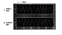
図6は,受信回路14を構成する復調回路14bの入力信号を示す図である。復調回路14bの入力信号は,局部発振回路11からの局部発振信号17(図6A)と,送受共用器13を減衰して通過する成分15aとアンテナ給電端からの反射波15bを含む送信信号の漏れ成分15(図6B)である。
FIG. 6 is a diagram illustrating an input signal of the
したがって,復調回路14bの動作が乗算であるとして,2倍波成分を省略したときに,復調回路14bの出力は(1)式で表される。
Therefore, assuming that the operation of the

式(1)において,復調回路の出力における位相雑音成分の大きさを決める項
In Equation (1), a term that determines the magnitude of the phase noise component in the output of the demodulation circuit
![]()
![]()
ただし,上記式において, However, in the above formula,
![]()
![]()
![]()
![]()
一方,位相雑音成分は, On the other hand, the phase noise component is
![]()
![]()
![]()
![]()
![]()
![]()
上記関係式から局部発振回路11からの局部発振信号と送信信号の漏れ15に対する復調回路14b入力までの経路がそれぞれ異なり,図6に示されるように復調回路への経路時間差がある場合,経路時間差τが大きくなるほど送信信号の漏れ15(図6B)と局部発振信号(図6A)の相関が小さくなり,復調回路14bから出力される雑音成分が大きくなることがわかる。図7は,経路時間差と雑音レベル(相対値)の関係を示すグラフである。図7のグラフから経路時間差τが大きくなるほど検波されてくる位相雑音レベルが大きくなり,経路時間差がなければ位相雑音成分は,ほぼキャンセルされることが理解できる。
From the above relational expression, when the path from the
従来技術として特許文献1に記載の発明がある。特許文献1には,質問器の送出する搬送波(キャリア)自身が持つ位相雑音と,同期検波に付随するPLL発振回路の位相雑音が復調信号に現れ,これにより受信感度が悪化することに触れている。そして,特許文献1に記載の発明は,質問器の同期検波での受信感度の低下を防止することを目的としている。
しかしながら,上記特許文献1に記載の発明は,タグからの応答信号を基準にローカル信号LOの位相を補正する構成である。かかる構成は,応答信号と送信信号の漏れの振幅・位相が殆ど変わらないシステム,即ち13.56MHz程度の低い周波数で応答器との距離が30cm程度の近距離を対象とするシステムにおいて効果を得ることが可能である。
However, the invention described in
しかし,UHF帯(860MHz〜960MHz)以上の周波数帯でRFID用送受信装置とICタグとの距離が数mでの利用の場合は,距離により位相は360°の10倍以上に変動する。 However, when the distance between the RFID transceiver device and the IC tag is a few meters in the frequency band of the UHF band (860 MHz to 960 MHz) or more, the phase fluctuates 10 times or more of 360 ° depending on the distance.
したがって,本発明の目的は,上記特許文献1に記載の発明では適用できない条件においても,タグとの距離に拘わらず雑音低下,従って高感度受信を可能とするRFID用送受信装置を提供することにある。
Accordingly, an object of the present invention is to provide an RFID transceiver device that can reduce noise regardless of the distance from the tag and thus can perform high-sensitivity reception even under conditions that are not applicable to the invention described in
上記の本発明の目的を達成するRFID用送受信装置の第1の態様は,局部発振信号を生成する局部発振回路と,前記局部発振回路から出力される局部発振信号の周波数を用いて,受信信号を復調する復調回路と,前記局部発振回路から出力される局部発振信号を変調および増幅して送信する送信回路と,前記送信回路からの送信信号を送受共用アンテナに供給し,前記送受共用アンテナで受信される受信信号を前記復調回路側に分岐する送受共用器と,更に,前記局部発振回路と前記復調回路との間に遅延回路を有し,前記遅延回路の遅延量が前記局部発振回路から出力され,送信される送信信号の前記送受共用器を経由して前記復調回路に入力する漏れ分の経路と,前記局部発振回路から前記復調回路に直接入力する経路との経路差に対応した大きさに設定されていることを特徴とする。 The first aspect of the RFID transceiver device that achieves the above-described object of the present invention is the reception signal using the local oscillation circuit that generates the local oscillation signal and the frequency of the local oscillation signal output from the local oscillation circuit. A demodulation circuit for demodulating the signal, a transmission circuit for modulating and amplifying the local oscillation signal output from the local oscillation circuit, and a transmission signal from the transmission circuit for supplying to the transmission / reception shared antenna, A duplexer for branching the received signal to the demodulator circuit side, and a delay circuit between the local oscillator circuit and the demodulator circuit, and the delay amount of the delay circuit from the local oscillator circuit The difference between the path of the leakage of the transmitted signal to be transmitted and input to the demodulation circuit via the duplexer and the path directly input to the demodulation circuit from the local oscillation circuit Characterized in that it is set to a size that is.
上記の本発明の目的を達成するRFID用送受信装置の第2の態様は,第1の態様において,
更に,前記復調回路の出力に基づき雑音レベルを検知する制御処理回路を有し,前記制御処理回路は,前記検知される雑音レベルに対応して前記遅延回路の遅延量をフィードバック制御することを特徴とする。
The second aspect of the RFID transceiver device that achieves the object of the present invention is as follows:
And a control processing circuit for detecting a noise level based on an output of the demodulation circuit, wherein the control processing circuit feedback-controls a delay amount of the delay circuit corresponding to the detected noise level. And
上記の本発明の目的を達成するRFID用送受信装置の第3の態様は,局部発振信号を生成する局部発振回路と,前記局部発振回路から出力される局部発振信号の周波数を用いて,受信信号を復調する復調回路と,前記局部発振回路から出力される局部発振信号を変調する変調回路と,前記変調回路から出力される送信信号を送受共用アンテナに供給し,前記送受共用アンテナで受信される受信信号を前記復調回路側に分岐する送受共用器と,更に,前記変調回路から出力される局部発振信号を前記復調回路に供給する経路とを有し,前記経路と,送信される送信信号の前記送受共用器を経由して前記復調回路に入力する漏れ分の経路における遅延量が同じ大きさに設定されていることを特徴とする。 The third aspect of the RFID transceiver device that achieves the above-described object of the present invention is the reception signal using the local oscillation circuit that generates the local oscillation signal and the frequency of the local oscillation signal output from the local oscillation circuit. A demodulation circuit that demodulates the signal, a modulation circuit that modulates a local oscillation signal output from the local oscillation circuit, and a transmission signal output from the modulation circuit is supplied to the shared antenna and is received by the shared antenna A duplexer for branching a received signal to the demodulation circuit side, and a path for supplying a local oscillation signal output from the modulation circuit to the demodulation circuit. The delay amount in the path of the leakage input to the demodulation circuit via the duplexer is set to the same size.
上記の本発明の目的を達成するRFID用送受信装置の第4の態様は,前記第1乃至3の態様のいずれかにおいて,更に送受共用アンテナと,前記送受共用アンテナと前記送受共用器を接続する遅延回路を有し,該遅延回路の遅延量は,前記送受共用器から前記送受共用アンテナ側を見たインピーダンスを特性インピーダンスにほぼ等しくするように設定されていることを特徴とする。 According to a fourth aspect of the RFID transceiver device that achieves the above-mentioned object of the present invention, in any one of the first to third aspects, the transmission / reception shared antenna, the transmission / reception shared antenna, and the duplexer are connected. A delay circuit is provided, and the delay amount of the delay circuit is set so that the impedance of the duplexer viewed from the duplexer is substantially equal to the characteristic impedance.
上記の本発明の目的を達成するRFID用送受信装置の第5の態様は,前記第2の態様において,前記制御処理回路における雑音レベルの検知は,前記送信回路からタグに向けてのコマンド送信を停止した状態で行うことを特徴とする。 According to a fifth aspect of the RFID transceiver device that achieves the above object of the present invention, in the second aspect, the noise level detection in the control processing circuit is performed by transmitting a command from the transmission circuit to the tag. It is characterized by being performed in a stopped state.
本発明の特徴は,以下に図面に従い説明される発明の実施の形態例から更に明らかになる。 The features of the present invention will become more apparent from the embodiments of the invention described below with reference to the drawings.
本発明により,タグとの距離に拘わらず雑音レベルを低下させ,従って高感度受信が可能であり,また,UHF帯以上の周波数におけるシステムの安定化を可能とするRFID用送受信装置が得られる。 According to the present invention, it is possible to obtain an RFID transceiver device that can reduce the noise level regardless of the distance to the tag, and thus can perform high-sensitivity reception and can stabilize the system at a frequency higher than the UHF band.
以下に図面に従い,本発明の実施の形態例を説明する。なお,実施の形態例は本発明の理解のためのものであり,本発明の技術的範囲がこれに限定されるものではない。 Embodiments of the present invention will be described below with reference to the drawings. The embodiments are for the purpose of understanding the present invention, and the technical scope of the present invention is not limited thereto.
図8は,本発明に従うRFID用送受信装置の第1の実施例ブロック図である。本実施例の特徴は,図5に示す従来構成との比較において局部発振回路11と復調回路14bとの間に遅延回路18を備えていることにある。
FIG. 8 is a block diagram of a first embodiment of an RFID transceiver device according to the present invention. The feature of this embodiment is that a
図8において,局部発振回路11から変調回路12b及び電力増幅器12cを通して送出される送信信号が送受共用器13から漏れて復調回路14bに至る漏れ信号15の経路は,局部発振回路11から復調回路14bに直接供給される局部発振信号17の経路よりも大きく,位相差が生じる。
In FIG. 8, the path of the
したがって,図8における特徴として,遅延回路18により局部発振回路11から復調回路14bに直接供給される局部発振信号17の経路に遅延を与えて漏れ信号15の経路を等しくする。これにより,図7に示したように,経路差が“0”である場合と同じになり,相対雑音レベルを最小にすることができる。
Therefore, as a feature in FIG. 8, the
図9は,本発明に従うRFID用送受信装置の第2の実施例ブロック図である。第2の実施例の特徴は,局部発振回路11から復調回路14bに供給される局部発振信号17の経路と,局部発振回路11から送受共用器13を経由する漏れ信号15の経路を実質的に等しくするように回路構成を組み合わせた点にある。
FIG. 9 is a block diagram of a second embodiment of the RFID transceiver device according to the present invention. The feature of the second embodiment is that the path of the
すなわち,局部発振回路11から復調回路14bに直接局部発振信号を供給せずに,電力増幅器12cの後段に結合回路12dを設けて,復調回路14bに供給される局部発振信号17と,送受共用器13を経由する漏れ信号15との経路の差を小さくする。さらに,存在する経路の微少差に対応する遅延量は,結合回路12dと復調回路14bとの間に微調回路18を設けて調整する。
That is, a local oscillation signal is not directly supplied from the
かかる図9の実施例においても復調回路14bに供給される局部発振信号17と,送受共用器13を経由する漏れ信号15との経路をほぼ同じにすることができるので,位相雑音を低減することができる。
In the embodiment of FIG. 9 as well, the path of the
図10は,更に第3の実施例である。この実施例の特徴は,図8の第1の実施例における遅延回路18の遅延量を受信検知される雑音レベルに応じて適応的に制御することにある。
FIG. 10 shows a third embodiment. The feature of this embodiment resides in that the delay amount of the
すなわち,復調回路14bの出力を増幅器14c及びローパスフィルタ14を通してA/D変換器14dに入力し,デジタル信号に変換する。A/D変換器14dのデジタル出力は,制御処理回路10に入力され,雑音レベルが判断される。
That is, the output of the
制御処理回路10は,雑音レベルに応じた補正量制御信号19を遅延回路18に送り対応する遅延量を与えるようにフィードバック制御する。これにより遅延量を雑音レベルに従って適応的に制御が可能である。制御処理回路10は,かかる制御を実行するために補正レベルと補正量制御信号との対応テーブルを備えて構成することが可能である。
The
図11は,図10における復調回路14bの構成例である。図12は,図11の復調回路を用いる場合の制御処理回路10の遅延回路18に対する処理フローである。また,図13は,遅延回路18における遅延量制御を説明する図である。
FIG. 11 is a configuration example of the
図11に戻り説明する。復調回路14bにおいて,受信信号RXを互いに直交するIチャネル信号とQチャネル信号に分離する直交分離回路141と,Iチャネル信号と局部発振回路11から出力される局部発振信号(LO)17を掛け算する乗算器142と,位相器144を通して局部発振回路11から出力される局部発振信号を90°移相してQチャネル信号と掛け算する乗算器143を有して構成される。
Returning to FIG. In the
図12において,キャリブレーションを行って遅延回路18の遅延量を設定する際は,RFID用送信装置からICタグに向けてのコマンドの送信を停止した状態で行う(ステップS1)。制御処理回路10は,復調回路14bから出力されるI,Qチャネル復調信号を入力とし,復調回路出力の初期電力P1(=I2+Q2)を求める(ステップS2)。
In FIG. 12, when performing the calibration and setting the delay amount of the
ここで,上記のように遅延回路18のキャリブレーションを行う際は,RFID用送信装置からICタグに向けてのコマンドの送信を停止した状態で行うので求めた電力(I2+Q2)は,経路差に基づく雑音レベルに相当する。
Here, when the calibration of the
ついで,遅延回路18の遅延量τをΔτ1増加する(ステップS3)。この時の復調回路14bの出力電力P2(=I2+Q2)を求める(ステップS4)。この遅延量τをΔτ1増加したときの電力P2と初期電力P1を比較する(ステップS5)。この電力比較において,P2<P1であれば(ステップS5,Yes),復調回路14bに直接入力される局部発振信号(LO)17の経路が大きくなる方向で送受共用器13を経由してくる漏れ成分との経路差が小さくなり,雑音レベルが小さくなることを示している。
Next, the delay amount τ of the
ここで,図13は,かかる経路差と雑音レベルとの関係を示している。さらに,図13Aにおいて,経路差が位相差λ/2に相当する点を中心に雑音レベルが増減する特性を示しおり,ここでは最小の雑音レベルがフィードバック制御の目標値である。 Here, FIG. 13 shows the relationship between the path difference and the noise level. Further, FIG. 13A shows a characteristic in which the noise level increases and decreases around the point where the path difference corresponds to the phase difference λ / 2. Here, the minimum noise level is the target value of the feedback control.
図13Bは,図13Aの経路差を正負に拡張して表現したもので,位相差λ/2に相当する経路差より小さな範囲で遅延回路18の遅延量を制御した場合に,最小の雑音レベルの目標値に向かう制御の方向を示している。
FIG. 13B expresses the path difference of FIG. 13A by expanding it positively and negatively. When the delay amount of the
前記ステップS5において,P2<P1となる場合は,図13Bにおいて,例えば制御の方向Iに対応していると理解できる。 In the step S5, when P2 <P1, it can be understood that it corresponds to, for example, the control direction I in FIG. 13B.
さらに,図12に戻り,P2<P1であれば(ステップS5,Yes),P1=P2として(ステップS6),ステップS3に戻り更に遅延量Δτ1を追加設定してステップS4以降の処理を継続する。 Furthermore, returning to FIG. 12, if P2 <P1 (step S5, Yes), P1 = P2 (step S6), returning to step S3, further setting the delay amount Δτ 1 and continuing the processing from step S4 onward. To do.
一方,ステップS5において,P2>P1であれば(ステップS5,No),遅延量τをΔτ2(<Δτ1)だけ小さくする方向に設定する(ステップS7)。次いで,この時の復調回路出力の電力P2(=I2+Q2)を求める(ステップS8)。この遅延量τをΔτ2減らしたときの電力P2と初期電力P1を比較する(ステップS9)。
この電力比較において,P2<P1であれば(ステップS9,Yes),送受共用器13からの漏れ成分15の経路に対し、局部発振回路11から復調回路14bへの直接の経路を小さくする方向で経路差が小さくなり,雑音レベルが小さくなることを示している。これは,先に説明した図13Bにおいて,制御の方向IIに対応している。
On the other hand, if P2> P1 in Step S5 (No in Step S5), the delay amount τ is set to be decreased by Δτ 2 (<Δτ 1 ) (Step S7). Next, the power P2 (= I 2 + Q 2 ) of the demodulation circuit output at this time is obtained (step S8). The power P2 when the delay amount τ is reduced by Δτ 2 is compared with the initial power P1 (step S9).
In this power comparison, if P2 <P1 (step S9, Yes), the direct path from the
したがって,目標値に向かうために,P1=P2として(ステップS10),ステップS7に戻り更に遅延量Δτ2を減らす設定をしてステップS7以降の処理を継続する。 Therefore, in order to go to the target value, P1 = P2 is set (step S10), the process returns to step S7 to further reduce the delay amount Δτ 2 and the processing after step S7 is continued.
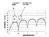
ここで,上記経路差の制御範囲(図13A参照)について考察する。直交変調の場合,図11に示すようにI,Q両チャネルの合成で最適値に設定することが必要である。図14は,図7に示した経路時間差と雑音レベル(相対値)を再掲した図であるが,IチャネルとQチャネルには90°の位相差があるために,一方のチャネルを最適にしても他方のチャネルの雑音レベルが大きくなる。 Here, the control range of the path difference (see FIG. 13A) will be considered. In the case of quadrature modulation, it is necessary to set an optimum value by combining both I and Q channels as shown in FIG. FIG. 14 shows the path time difference and the noise level (relative value) shown in FIG. 7 again. Since the I channel and the Q channel have a phase difference of 90 °, one channel is optimized. However, the noise level of the other channel increases.
例えば,図14において,Iチャネルを−85dBに設定したとしてもQチャネルはIチャネルに対して90°の位相差があるので,−40dBと雑音レベルが大きくなる(図14,A参照)。したがって,I,Qの合成で最適値になるように制御する(図14,B参照)。 For example, in FIG. 14, even if the I channel is set to −85 dB, the Q channel has a phase difference of 90 ° with respect to the I channel, so that the noise level increases to −40 dB (see FIG. 14A). Therefore, control is performed so that the optimum value is obtained by combining I and Q (see FIG. 14B).
図15は,I,Q両チャネルの雑音の和(I2+Q2)について,経路時間差と雑音レベル(相対値)について求めたグラフである。図15において,例えば,経路時間差0.5(経路差λ/2)にあるとき,遅延回路18の遅延量を制御して経路時間差を0.2(経路差λ/5)に補正することにより10dB雑音レベルが改善する(図15,II→I参照)。
FIG. 15 is a graph obtained for the path time difference and the noise level (relative value) for the noise sum (I 2 + Q 2 ) of both the I and Q channels. In FIG. 15, for example, when the path time difference is 0.5 (path difference λ / 2), the delay time of the
次に,図16は更に本発明の別の実施例を示す図である。この実施例の特徴は,送受共用器13とアンテナ16の給電端との間に遅延回路20を設けた構成にある。ここで,送受共用器のポート割当は,TX端→ANT端は通過,TX端→RX端は阻止,ANT端→RX端は結合となるようにしてある。
Next, FIG. 16 is a diagram showing still another embodiment of the present invention. This embodiment is characterized in that a
ここで,遅延回路20は,実施例として,図17に示すように送受共用器13とアンテナ(図中では負荷ZL)との間に配置した線路長lの遅延線DLにより構成する。この遅延線DLによりアンテナ16と送受共用器13との線路長lが調整できる。
Here, as an embodiment, the
線路長l,アンテナ負荷インピーダンスZL,線路の特性インピーダンスZ0とすると送受共用器からアンテナ側を見たインピーダンスZは,次のようになる。 Assuming that the line length l, the antenna load impedance Z L , and the line characteristic impedance Z 0 , the impedance Z seen from the duplexer as viewed from the antenna side is as follows.
一方,アンテナ側インピーダンスZにより送信信号の漏れ量が変化する。したがって,遅延回路20として挿入した遅延線DLなどにより給電端までの線路長lを調整して漏れ量を制御することができる。送受共用器13の結合度(送信側(TX)端→受信側(RX)端)は、アンテナ端インピーダンスが特性インピーダンスZ0に一致するとき、理論的には無限小(0)になる。しかし,実際の回路では−40dB程度が限界である。
On the other hand, the leakage amount of the transmission signal changes depending on the antenna side impedance Z. Therefore, the amount of leakage can be controlled by adjusting the line length l to the feeding end by using the delay line DL or the like inserted as the
このように,本発明の実施例において,遅延回路20を設け,遅延回路20の線路長を調整することにより,送受共用器からアンテナ側を見たインピーダンスZを,より特性インピーダンスに近づけることにより送信信号の復調回路側への漏れ量を小さくすることができる。
As described above, in the embodiment of the present invention, the
なお,図16における共用アンテナ16と送受共用器13の間に遅延回路20を備える構成は,先に説明した図5,図8及び,図9の実施の形態例においても適用可能である。
The configuration including the
図19は,図16の実施例を拡張する例である。複数のICタグに対して共通のRFID送受信装置を使用する場合,切換器21により複数のアンテナ16a〜16dを切換接続する。
かかる実施例においても図16の実施例の原理が適用可能である。すなわち,切換器21と各アンテナ16a〜16dとの間に遅延回路22a〜22dを挿入する。
FIG. 19 shows an example of extending the embodiment of FIG. When a common RFID transceiver device is used for a plurality of IC tags, a plurality of
Also in this embodiment, the principle of the embodiment of FIG. 16 can be applied. That is, delay circuits 22a to 22d are inserted between the
遅延回路22a〜22dのそれぞれにおける線路長を調整して対応するアンテナ端インピーダンスを特性インピーダンスに近づけることにより,送信信号の復調回路14bへの漏れを最小にすることが可能である。
By adjusting the line length in each of the delay circuits 22a to 22d and bringing the corresponding antenna end impedance close to the characteristic impedance, it is possible to minimize the leakage of the transmission signal to the
上記に図面に従い説明したように,本発明によりタグとの距離に拘わらず雑音を低下させ,高感度受信を可能とするRFID用送受信装置が提供される。したがって,高信頼性のRFIDシステムの構築が可能である。 As described above with reference to the drawings, the present invention provides an RFID transceiver device capable of reducing noise regardless of the distance from a tag and enabling high-sensitivity reception. Therefore, it is possible to construct a highly reliable RFID system.
1 RFID用送受信装置
2 ICタグ
10 制御処理回路
11 局部発振回路
12 送信回路
13 送受共用器
14 受信回路
15 送信信号の漏れ
16 アンテナ
DESCRIPTION OF
Claims (5)
前記局部発振回路から出力される局部発振信号の周波数を用いて受信信号を復調する復調回路と,
前記局部発振回路から出力される局部発振信号を変調および増幅して送信する送信回路と,
前記送信回路からの送信信号を送受共用アンテナに供給し,前記送受共用アンテナで受信される受信信号を前記復調回路側に分岐する送受共用器と,
前記局部発振回路と前記復調回路との間に遅延回路を有し,
前記遅延回路の遅延量が、前記局部発振回路から出力され送信される送信信号の前記送受共用器を経由して前記復調回路に入力する漏れ分の経路と,前記局部発振回路から前記復調回路に直接入力する局部発振信号の経路との経路差に対応した大きさに設定されている
ことを特徴とするRFID用送受信装置。 A local oscillation circuit for generating a local oscillation signal;
A demodulation circuit that demodulates a received signal using the frequency of the local oscillation signal output from the local oscillation circuit;
A transmission circuit that modulates and amplifies and transmits a local oscillation signal output from the local oscillation circuit;
A transmission / reception unit for supplying a transmission signal from the transmission circuit to a transmission / reception antenna, and branching a reception signal received by the transmission / reception antenna to the demodulation circuit side;
A delay circuit between the local oscillation circuit and the demodulation circuit;
The amount of delay of the delay circuit is a path of leakage that is input from the local oscillator circuit to the demodulator circuit via the duplexer of the transmission signal output and transmitted from the local oscillator circuit, and from the local oscillator circuit to the demodulator circuit. An RFID transceiver device characterized by being set to a size corresponding to a path difference from a path of a local oscillation signal inputted directly.
更に,前記復調回路の出力に基づき雑音レベルを検知する制御処理回路を有し,
前記制御処理回路は,前記検知される雑音レベルに基づいて前記遅延回路の遅延量を制御することを特徴とするRFID用送受信装置。 In claim 1,
And a control processing circuit for detecting a noise level based on the output of the demodulation circuit,
The RFID processing apparatus, wherein the control processing circuit controls a delay amount of the delay circuit based on the detected noise level.
前記局部発振回路から出力される局部発振信号の周波数を用いて受信信号を復調する復調回路と,
前記局部発振回路から出力される局部発振信号を変調する変調回路と,
前記変調回路から出力される送信信号を送受共用アンテナに供給し,前記送受共用アンテナで受信される受信信号を前記復調回路側に分岐する送受共用器と,
前記変調回路から出力される送信信号を局部発振信号として前記復調回路に供給する経路とを有し,
前記経路と,送信されるキャリア信号の前記送受共用器を経由して前記復調回路に入力する漏れ分の経路における遅延量が同じ大きさに設定されている
ことを特徴とするRFID用送受信装置。 A local oscillation circuit for generating a local oscillation signal;
A demodulation circuit that demodulates a received signal using the frequency of the local oscillation signal output from the local oscillation circuit;
A modulation circuit for modulating a local oscillation signal output from the local oscillation circuit;
A transmission / reception unit for supplying a transmission signal output from the modulation circuit to a transmission / reception antenna, and branching a reception signal received by the transmission / reception antenna to the demodulation circuit side;
A path for supplying a transmission signal output from the modulation circuit to the demodulation circuit as a local oscillation signal,
The RFID transmission / reception apparatus, wherein the delay amount of the path and the leakage path of the carrier signal to be transmitted that is input to the demodulation circuit via the duplexer is set to the same magnitude.
更に送受共用アンテナと,
前記送受共用アンテナと前記送受共用器を接続する遅延回路を有し,
該遅延回路の遅延量は,前記送受共用器から見た前記送受共用アンテナ側インピーダンスを特性インピーダンスにほぼ等しくするように設定されていることを特徴とするRFID用送受信装置。 In any one of Claims 1 thru | or 3,
In addition, a shared antenna for transmission and reception,
A delay circuit that connects the duplex antenna and the duplexer;
The RFID transmission / reception apparatus, wherein the delay amount of the delay circuit is set so that the impedance of the transmitting / receiving antenna side viewed from the transmitting / receiving duplexer is substantially equal to the characteristic impedance.
前記制御処理回路における雑音レベルの検知は,前記送信回路からタグに向けてのコマンド送信を停止した状態で行うことを特徴とするRFID用送受信装置。 In claim 2,
The RFID transceiver device, wherein the detection of the noise level in the control processing circuit is performed in a state where command transmission from the transmission circuit to the tag is stopped.
Priority Applications (7)
| Application Number | Priority Date | Filing Date | Title |
|---|---|---|---|
| JP2005111531A JP4387323B2 (en) | 2005-04-08 | 2005-04-08 | RFID transceiver |
| TW094127722A TWI279992B (en) | 2005-04-08 | 2005-08-15 | RFID transceiver device |
| DE602005014938T DE602005014938D1 (en) | 2005-04-08 | 2005-08-16 | RFID transceiver |
| EP05255049A EP1710727B1 (en) | 2005-04-08 | 2005-08-16 | RFID transceiver device |
| US11/209,627 US7492812B2 (en) | 2005-04-08 | 2005-08-24 | RFID transceiver device |
| KR1020050083620A KR100731227B1 (en) | 2005-04-08 | 2005-09-08 | Rfid transceiver device |
| CN2005101025863A CN1845469B (en) | 2005-04-08 | 2005-09-12 | Rfid transceiver device |
Applications Claiming Priority (1)
| Application Number | Priority Date | Filing Date | Title |
|---|---|---|---|
| JP2005111531A JP4387323B2 (en) | 2005-04-08 | 2005-04-08 | RFID transceiver |
Publications (2)
| Publication Number | Publication Date |
|---|---|
| JP2006295419A JP2006295419A (en) | 2006-10-26 |
| JP4387323B2 true JP4387323B2 (en) | 2009-12-16 |
Family
ID=36675932
Family Applications (1)
| Application Number | Title | Priority Date | Filing Date |
|---|---|---|---|
| JP2005111531A Active JP4387323B2 (en) | 2005-04-08 | 2005-04-08 | RFID transceiver |
Country Status (7)
| Country | Link |
|---|---|
| US (1) | US7492812B2 (en) |
| EP (1) | EP1710727B1 (en) |
| JP (1) | JP4387323B2 (en) |
| KR (1) | KR100731227B1 (en) |
| CN (1) | CN1845469B (en) |
| DE (1) | DE602005014938D1 (en) |
| TW (1) | TWI279992B (en) |
Families Citing this family (37)
| Publication number | Priority date | Publication date | Assignee | Title |
|---|---|---|---|---|
| US7327802B2 (en) * | 2004-03-19 | 2008-02-05 | Sirit Technologies Inc. | Method and apparatus for canceling the transmitted signal in a homodyne duplex transceiver |
| US7545272B2 (en) | 2005-02-08 | 2009-06-09 | Therasense, Inc. | RF tag on test strips, test strip vials and boxes |
| JP4387323B2 (en) * | 2005-04-08 | 2009-12-16 | 富士通株式会社 | RFID transceiver |
| US8226003B2 (en) | 2006-04-27 | 2012-07-24 | Sirit Inc. | Adjusting parameters associated with leakage signals |
| KR100716018B1 (en) * | 2006-05-17 | 2007-05-08 | 한국과학기술원 | Mobile-embedded rfid interrogator and method for canceling tx leakage thereof |
| KR101184702B1 (en) * | 2006-09-21 | 2012-09-20 | 삼성전자주식회사 | mRFID READER |
| KR100819045B1 (en) * | 2006-11-08 | 2008-04-02 | 한국전자통신연구원 | Apparatus and method to optimize the output power of rfid reader |
| KR100789369B1 (en) | 2006-11-14 | 2007-12-28 | 한국전자통신연구원 | Rfid reader for restricting transmission leakage signal |
| KR100996104B1 (en) * | 2006-12-29 | 2010-11-22 | 삼성전자주식회사 | Receiving sensitivity improvement device and method for portable radio frequency identification |
| KR101372060B1 (en) * | 2007-01-30 | 2014-03-07 | 엘지이노텍 주식회사 | Radio Frequency IDentification receiver system using demodulation carrier variable |
| US8855029B2 (en) * | 2007-03-21 | 2014-10-07 | Skyworks Solutions, Inc. | LMS adaptive filter for digital cancellation of second order inter-modulation due to transmitter leakage |
| WO2008116153A1 (en) * | 2007-03-21 | 2008-09-25 | Skyworks Solutions, Inc. | Lms adaptive filter for digital cancellation of second order inter-modulation due to transmitter leakage |
| US8248212B2 (en) | 2007-05-24 | 2012-08-21 | Sirit Inc. | Pipelining processes in a RF reader |
| JP5060193B2 (en) * | 2007-07-18 | 2012-10-31 | 京セラドキュメントソリューションズ株式会社 | Data transmitting / receiving apparatus and image forming apparatus |
| KR100932064B1 (en) * | 2007-09-04 | 2009-12-15 | 한국전자통신연구원 | RDF tag and its control method |
| US8427316B2 (en) | 2008-03-20 | 2013-04-23 | 3M Innovative Properties Company | Detecting tampered with radio frequency identification tags |
| US8446256B2 (en) * | 2008-05-19 | 2013-05-21 | Sirit Technologies Inc. | Multiplexing radio frequency signals |
| EP2329429A4 (en) * | 2008-09-17 | 2015-07-29 | Semiconductor Energy Lab | Semiconductor device |
| US8760520B2 (en) * | 2008-11-10 | 2014-06-24 | Eduard Levin | System and method for tracking and monitoring personnel and equipment |
| US8169312B2 (en) * | 2009-01-09 | 2012-05-01 | Sirit Inc. | Determining speeds of radio frequency tags |
| US8036606B2 (en) * | 2009-02-03 | 2011-10-11 | Ubidyne, Inc. | Method and apparatus for interference cancellation |
| US8421601B2 (en) * | 2009-03-22 | 2013-04-16 | International Business Machines Corporation | Active/passive RFID transponder control function |
| US20100289623A1 (en) * | 2009-05-13 | 2010-11-18 | Roesner Bruce B | Interrogating radio frequency identification (rfid) tags |
| US8416079B2 (en) * | 2009-06-02 | 2013-04-09 | 3M Innovative Properties Company | Switching radio frequency identification (RFID) tags |
| US20110205025A1 (en) * | 2010-02-23 | 2011-08-25 | Sirit Technologies Inc. | Converting between different radio frequencies |
| CN101794370B (en) * | 2010-04-09 | 2012-01-11 | 深圳市远望谷信息技术股份有限公司 | Method and device for remotely testing receiver sensitivity of radio frequency identification reader |
| KR20110124042A (en) * | 2010-05-10 | 2011-11-16 | 삼성테크윈 주식회사 | Reader of rfid wherein phase noise is removed |
| JP5857343B2 (en) * | 2010-07-07 | 2016-02-10 | オプテックス株式会社 | Passive infrared sensor |
| JP5633270B2 (en) * | 2010-09-16 | 2014-12-03 | 株式会社リコー | Transceiver |
| CN102148724B (en) * | 2011-01-31 | 2014-12-31 | 中兴通讯股份有限公司 | Link detecting method and network access device |
| US10062025B2 (en) | 2012-03-09 | 2018-08-28 | Neology, Inc. | Switchable RFID tag |
| US8781049B1 (en) * | 2012-12-27 | 2014-07-15 | Intel Mobile Communications GmbH | Signal delay estimator with absolute delay amount and direction estimation |
| CN104883199A (en) * | 2015-05-12 | 2015-09-02 | 惠州Tcl移动通信有限公司 | Wireless terminal and data receiving and transmitting method thereof |
| CN106815625B (en) * | 2015-12-02 | 2020-03-20 | 四川华大恒芯科技有限公司 | Demodulation circuit suitable for ultra-low power consumption design |
| US20170302429A1 (en) * | 2016-04-15 | 2017-10-19 | Andrew Wireless Systems Gmbh | Duplexing and combining networks |
| CN107359947B (en) * | 2016-11-07 | 2020-09-15 | 天地融科技股份有限公司 | Circuit time delay self-detection device and system |
| US20220360362A1 (en) * | 2021-05-06 | 2022-11-10 | Apple Inc. | Systems and methods for high power operation in user equipment |
Family Cites Families (18)
| Publication number | Priority date | Publication date | Assignee | Title |
|---|---|---|---|---|
| GB2300318B (en) | 1981-02-10 | 1997-03-19 | Plessey Co Ltd | Improvements in or relating to transceivers |
| CA2077500C (en) | 1991-09-04 | 1996-09-17 | Yukio Yokoyama | Radio transceiver |
| JPH08122429A (en) * | 1994-10-25 | 1996-05-17 | Sumitomo Electric Ind Ltd | Interference compensator for mobile identification system |
| GB9423027D0 (en) * | 1994-11-15 | 1995-01-04 | Univ Bristol | Full-duplex radio transmitter/receiver |
| JPH0969799A (en) * | 1995-09-01 | 1997-03-11 | Antenna Giken Kk | Automatic control circulator device |
| US6311045B1 (en) * | 1997-07-28 | 2001-10-30 | Roke Manor Research Limited | Apparatus for signal isolation in a radio transmitter-receiver |
| JP3670454B2 (en) * | 1997-08-28 | 2005-07-13 | 株式会社日立国際電気 | Non-contact IC card system |
| JPH11261436A (en) * | 1998-03-10 | 1999-09-24 | Sony Corp | Amplifier circuit, and transmission/reception device |
| JPH11331897A (en) * | 1998-05-19 | 1999-11-30 | Nec Shizuoka Ltd | Radio selective calling receiver with notice holding function and radio selective calling reception method |
| WO2000005692A1 (en) * | 1998-07-24 | 2000-02-03 | Checkpoint Systems, Inc. | Rfid system for detecting low power resonant tags |
| US6686830B1 (en) * | 2000-06-28 | 2004-02-03 | Applied Wireless Identifications Group | Homodyne I/Q transceiver for a spread spectrum reader |
| DE60115158T2 (en) * | 2000-06-28 | 2006-06-29 | Thomson Licensing | High-frequency oscillator |
| WO2002017506A1 (en) * | 2000-08-22 | 2002-02-28 | Novatel Wireless, Inc. | Method and apparatus for transmitter noise cancellation in an rf communications system |
| US7253717B2 (en) | 2000-11-29 | 2007-08-07 | Mobile Technics Llc | Method and system for communicating with and tracking RFID transponders |
| JP2003174388A (en) * | 2001-12-06 | 2003-06-20 | Hitachi Kokusai Electric Inc | Demodulation circuit of questioning unit |
| US7330500B2 (en) * | 2001-12-07 | 2008-02-12 | Socovar S.E.C. | Adjustable electronic duplexer |
| KR20050011046A (en) * | 2003-07-21 | 2005-01-29 | (주)텔리뷰 | Direct demodulating apparatus and method using a frequency shifter |
| JP4387323B2 (en) * | 2005-04-08 | 2009-12-16 | 富士通株式会社 | RFID transceiver |
-
2005
- 2005-04-08 JP JP2005111531A patent/JP4387323B2/en active Active
- 2005-08-15 TW TW094127722A patent/TWI279992B/en active
- 2005-08-16 EP EP05255049A patent/EP1710727B1/en active Active
- 2005-08-16 DE DE602005014938T patent/DE602005014938D1/en active Active
- 2005-08-24 US US11/209,627 patent/US7492812B2/en active Active
- 2005-09-08 KR KR1020050083620A patent/KR100731227B1/en active IP Right Grant
- 2005-09-12 CN CN2005101025863A patent/CN1845469B/en active Active
Also Published As
| Publication number | Publication date |
|---|---|
| EP1710727A1 (en) | 2006-10-11 |
| US7492812B2 (en) | 2009-02-17 |
| CN1845469B (en) | 2010-05-05 |
| DE602005014938D1 (en) | 2009-07-30 |
| CN1845469A (en) | 2006-10-11 |
| EP1710727B1 (en) | 2009-06-17 |
| KR100731227B1 (en) | 2007-06-22 |
| KR20060106588A (en) | 2006-10-12 |
| TW200637203A (en) | 2006-10-16 |
| US20060229032A1 (en) | 2006-10-12 |
| JP2006295419A (en) | 2006-10-26 |
| TWI279992B (en) | 2007-04-21 |
Similar Documents
| Publication | Publication Date | Title |
|---|---|---|
| JP4387323B2 (en) | RFID transceiver | |
| JP4524674B2 (en) | Interrogator for RFID tag communication system | |
| US7369811B2 (en) | System and method for sensitivity optimization of RF receiver using adaptive nulling | |
| JP4962298B2 (en) | Transceiver | |
| US20060252398A1 (en) | Receiver of RFID reader for eliminating leakage signal | |
| EP1741213B1 (en) | A method and apparatus for canceling the transmitted signal in a homodyne duplex transceiver | |
| US8120464B2 (en) | RFID reader and method for removing a transmission carrier leakage signal | |
| US20080080599A1 (en) | Heterodyne rf transceiver for radar sensor | |
| US8410905B2 (en) | RFID reader cancelling leakage signal | |
| JP4516029B2 (en) | Reader / writer device | |
| JP4537248B2 (en) | Carrier sense method and transmitting / receiving apparatus | |
| US8010046B2 (en) | Wireless communication apparatus | |
| JPH1062518A (en) | Carrier phase noise-suppressing circuit | |
| EP2266072B1 (en) | Method for reducing a noise in a signal received in a contactless-card interrogator and a circuit to perform said method | |
| JP2011239401A (en) | Transmitter receiver capable of removing phase noise | |
| JP4095632B2 (en) | Interrogator | |
| US7809334B2 (en) | Signal transmitting and receiving apparatus capable of preventing the receiving end from saturating | |
| KR20100035411A (en) | Rfid reader and method for cancelling leakaged signal | |
| JPH0627228A (en) | Single oscillator fsk pulse radar transmitter-receiver | |
| US10103706B2 (en) | Transmission and reception device | |
| KR20200073136A (en) | Transmitter for reducing leakage power | |
| KR101489881B1 (en) | Rfid reader cancelling leakaged signal | |
| JP5053310B2 (en) | Transceiver circuit and signal receiving method thereof | |
| KR101417035B1 (en) | Radio Frequency tranceiver device | |
| US7383026B1 (en) | Wideband retroreflector |
Legal Events
| Date | Code | Title | Description |
|---|---|---|---|
| A621 | Written request for application examination |
Free format text: JAPANESE INTERMEDIATE CODE: A621 Effective date: 20080116 |
|
| A977 | Report on retrieval |
Free format text: JAPANESE INTERMEDIATE CODE: A971007 Effective date: 20090915 |
|
| TRDD | Decision of grant or rejection written | ||
| A01 | Written decision to grant a patent or to grant a registration (utility model) |
Free format text: JAPANESE INTERMEDIATE CODE: A01 Effective date: 20090929 |
|
| A01 | Written decision to grant a patent or to grant a registration (utility model) |
Free format text: JAPANESE INTERMEDIATE CODE: A01 |
|
| A61 | First payment of annual fees (during grant procedure) |
Free format text: JAPANESE INTERMEDIATE CODE: A61 Effective date: 20090930 |
|
| R150 | Certificate of patent or registration of utility model |
Ref document number: 4387323 Country of ref document: JP Free format text: JAPANESE INTERMEDIATE CODE: R150 Free format text: JAPANESE INTERMEDIATE CODE: R150 |
|
| FPAY | Renewal fee payment (event date is renewal date of database) |
Free format text: PAYMENT UNTIL: 20121009 Year of fee payment: 3 |
|
| FPAY | Renewal fee payment (event date is renewal date of database) |
Free format text: PAYMENT UNTIL: 20121009 Year of fee payment: 3 |
|
| FPAY | Renewal fee payment (event date is renewal date of database) |
Free format text: PAYMENT UNTIL: 20131009 Year of fee payment: 4 |
|
| S111 | Request for change of ownership or part of ownership |
Free format text: JAPANESE INTERMEDIATE CODE: R313117 |
|
| R350 | Written notification of registration of transfer |
Free format text: JAPANESE INTERMEDIATE CODE: R350 |