JP4376231B2 - Dielectric resonator loaded oscillation circuit and radar device using the same - Google Patents
Dielectric resonator loaded oscillation circuit and radar device using the same Download PDFInfo
- Publication number
- JP4376231B2 JP4376231B2 JP2006006716A JP2006006716A JP4376231B2 JP 4376231 B2 JP4376231 B2 JP 4376231B2 JP 2006006716 A JP2006006716 A JP 2006006716A JP 2006006716 A JP2006006716 A JP 2006006716A JP 4376231 B2 JP4376231 B2 JP 4376231B2
- Authority
- JP
- Japan
- Prior art keywords
- dielectric resonator
- oscillation circuit
- voltage
- switch
- power supply
- Prior art date
- Legal status (The legal status is an assumption and is not a legal conclusion. Google has not performed a legal analysis and makes no representation as to the accuracy of the status listed.)
- Expired - Fee Related
Links
Images


Classifications
-
- H—ELECTRICITY
- H03—ELECTRONIC CIRCUITRY
- H03B—GENERATION OF OSCILLATIONS, DIRECTLY OR BY FREQUENCY-CHANGING, BY CIRCUITS EMPLOYING ACTIVE ELEMENTS WHICH OPERATE IN A NON-SWITCHING MANNER; GENERATION OF NOISE BY SUCH CIRCUITS
- H03B5/00—Generation of oscillations using amplifier with regenerative feedback from output to input
- H03B5/18—Generation of oscillations using amplifier with regenerative feedback from output to input with frequency-determining element comprising distributed inductance and capacitance
- H03B5/1864—Generation of oscillations using amplifier with regenerative feedback from output to input with frequency-determining element comprising distributed inductance and capacitance the frequency-determining element being a dielectric resonator
- H03B5/187—Generation of oscillations using amplifier with regenerative feedback from output to input with frequency-determining element comprising distributed inductance and capacitance the frequency-determining element being a dielectric resonator the active element in the amplifier being a semiconductor device
- H03B5/1876—Generation of oscillations using amplifier with regenerative feedback from output to input with frequency-determining element comprising distributed inductance and capacitance the frequency-determining element being a dielectric resonator the active element in the amplifier being a semiconductor device the semiconductor device being a field-effect device
Description
本発明は誘電体共振器装荷型発振回路に関し、特に、パルス変調方式を用いたレーダー装置への適用が好適な誘電体共振器装荷型発振回路に関する。また、本発明はレーダー装置に関し、特に、誘電体共振器装荷型発振回路を用いてキャリア信号を生成し、パルス変調波を生成して出力するレーダー装置に関する。 The present invention relates to a dielectric resonator loaded oscillation circuit, and more particularly to a dielectric resonator loaded oscillation circuit suitable for application to a radar device using a pulse modulation method. The present invention also relates to a radar apparatus, and more particularly to a radar apparatus that generates a carrier signal using a dielectric resonator loaded oscillation circuit and generates and outputs a pulse modulated wave.
近年、マイクロ波やミリ波を利用したレーダー装置が数多く提案されている。このようなレーダー装置の応用範囲は様々であるが、例えばこれを自動車に搭載すれば、先行車両や後続車両との距離を正確に検出することが可能となるばかりでなく、ドライバーの死角となる位置、例えば、斜め後方やバンパーの近傍に存在する障害物を検知してドライバーに注意を促したり、さらには、避けられない衝突が迫っていることを検知してシートベルトを締め付けるなどのプレクラッシュ制御を行うことが可能となる。 In recent years, many radar devices using microwaves and millimeter waves have been proposed. The range of application of such a radar device is various. For example, if it is mounted on an automobile, it is possible not only to accurately detect the distance from the preceding vehicle and the following vehicle, but also to be a driver's blind spot. Pre-crash such as detecting obstacles in the position, for example, diagonally behind or near the bumper to alert the driver, or even detecting the inevitable collision approaching and tightening the seat belt Control can be performed.
このようなレーダー装置が自動車に数多く搭載されるようになると、レーダー装置間における干渉の問題が浮上する。つまり、レーダー装置を搭載した車両同士が近づいた場合や、同じ車両に複数のレーダー装置が搭載されている場合には、レーダー装置間の距離が近いために強い干渉が生じ、その結果、正確な計測が妨げられるという問題があった。 When many such radar devices are mounted on automobiles, the problem of interference between the radar devices will emerge. In other words, when vehicles equipped with radar devices approach each other, or when multiple radar devices are mounted on the same vehicle, strong interference occurs because the distance between the radar devices is short, resulting in accurate There was a problem that the measurement was hindered.
レーダー装置間の干渉を防止する方法としては、例えば特許文献1に記載された方法が知られている。特許文献1に記載された方法は、干渉波を受信して位相を反転させ、これを再送信する干渉防止装置を設置するというものである。しかしながら、広範囲に亘って干渉を防止するためには、多くの干渉防止装置を設置しなければならないだけでなく、干渉防止装置が設置されていないエリアでは干渉を全く防止することができないという問題があった。しかも、車載用レーダーの場合には、レーダー装置間の位置関係が常に一定になるとは限らないことから、特許文献1に記載された方法では、干渉の問題を解決することは困難である。
干渉の問題を解決する別の方法として、パルス変調方式のレーダー装置の場合、送受信動作を行っていない期間においてキャリア信号の生成を停止させるという方法が考えられる。一般に、パルス変調方式を用いたレーダー装置では、送受信動作を行う期間よりも送受信動作を行っていない期間の方がはるかに長く、このため、送受信動作を行っていない期間においてキャリア信号の生成を停止すれば、他のレーダー装置に対する干渉の影響を大幅に低減することが可能となる。 As another method for solving the interference problem, in the case of a pulse modulation type radar device, a method of stopping generation of a carrier signal during a period in which no transmission / reception operation is performed can be considered. In general, in a radar device using a pulse modulation method, a period in which no transmission / reception operation is performed is much longer than a period in which transmission / reception operation is performed. Therefore, generation of a carrier signal is stopped in a period in which no transmission / reception operation is performed. By doing so, it becomes possible to significantly reduce the influence of interference on other radar devices.
しかしながら、キャリア信号を生成する発振回路にはある程度の立ち上がり時間が存在することから、一旦停止させた発振回路の動作再開は、この立ち上がり時間を考慮して早めに行う必要がある。具体的には、実際に送受信を開始するタイミングから発振回路の立ち上がり時間以上前に、発振回路の動作開始を行う必要がある。一方、発振回路にはある程度の立ち下がり時間が存在することから、発振回路の動作を停止させても、立ち下がり時間が経過するまでの間は発振が持続してしまう。このように、発振回路の立ち上がり時間や立ち下がり時間が長いと、実際に発振回路が発振している期間が長くなることが分かる。したがって、他のレーダー装置に対する干渉の影響を十分に低減するためには、発振回路の立ち上がり時間や立ち下がり時間をできるだけ短縮することが必要である。 However, since an oscillation circuit that generates a carrier signal has a certain rise time, it is necessary to restart the operation of the oscillation circuit once stopped in consideration of the rise time. Specifically, it is necessary to start the operation of the oscillation circuit at least before the rise time of the oscillation circuit from the timing of actually starting transmission / reception. On the other hand, since there is a certain fall time in the oscillation circuit, even if the operation of the oscillation circuit is stopped, oscillation continues until the fall time elapses. Thus, it can be seen that if the rise time and fall time of the oscillation circuit are long, the period during which the oscillation circuit actually oscillates becomes long. Therefore, in order to sufficiently reduce the influence of interference on other radar devices, it is necessary to shorten the rise time and fall time of the oscillation circuit as much as possible.
パルス変調方式を用いたレーダー装置においては、キャリア信号を生成するための発振回路として、誘電体共振器を利用した発振回路、つまり、誘電体共振器装荷型発振回路が広く用いられているが、誘電体共振器装荷型発振回路は特に立ち下がり時間が長いことが多く、このため、他のレーダー装置に対する干渉の影響を低減するためには、立ち下がり時間の短縮が最も強く求められる。 In radar devices using a pulse modulation method, an oscillation circuit using a dielectric resonator, that is, a dielectric resonator loaded oscillation circuit is widely used as an oscillation circuit for generating a carrier signal. Dielectric resonator loaded oscillation circuits often have a particularly long fall time. Therefore, in order to reduce the influence of interference on other radar devices, the reduction of the fall time is most strongly required.
したがって、本発明の目的は、立ち上がり時間及び/又は立ち下がり時間の短い誘電体共振器装荷型発振回路及びこれを用いたレーダー装置を提供することである。 Accordingly, an object of the present invention is to provide a dielectric resonator loaded oscillation circuit having a short rise time and / or a short fall time, and a radar device using the same.
本発明による誘電体共振器装荷型発振回路は、誘電体共振器と、前記誘電体共振器に共振電圧を与える駆動回路と、前記共振電圧を生成するために必要な第1の電圧及び前記共振電圧の生成を停止させる第2の電圧を前記駆動回路に与える手段とを備えることを特徴とする。 A dielectric resonator loaded oscillation circuit according to the present invention includes a dielectric resonator, a drive circuit that applies a resonance voltage to the dielectric resonator, a first voltage required to generate the resonance voltage, and the resonance. And means for supplying a second voltage for stopping the generation of the voltage to the driving circuit.
本発明によれば、発振を開始する場合には第1の電圧を駆動回路に印加し、発振を停止する場合には第2の電圧を駆動回路に印加することができることから、立ち上がり時間及び/又は立ち下がり時間を短縮することが可能となる。 According to the present invention, when the oscillation is started, the first voltage can be applied to the drive circuit, and when the oscillation is stopped, the second voltage can be applied to the drive circuit. Alternatively, the fall time can be shortened.
駆動回路は、トランジスタと、トランジスタの被制御電極及び制御電極にそれぞれ接続された第1及び第2の信号線路とを含むことが好ましい。 The drive circuit preferably includes a transistor and first and second signal lines connected to the controlled electrode and the control electrode of the transistor, respectively.
前記手段は、トランジスタの被制御電極と第1の電圧が供給される第1の電源端子との間に設けられた第1のスイッチと、トランジスタの被制御電極と第2の電圧が供給される第2の電源端子との間に設けられた第2のスイッチとを含み、第1及び第2のスイッチは排他的に導通することが好ましい。これによれば、発振を停止させる場合、第2のスイッチをオンさせることにより、トランジスタの被制御電極に蓄積された電荷を放出することができることから、立ち下がり時間を大幅に短縮することが可能となる。 The means is provided with a first switch provided between a controlled electrode of the transistor and a first power supply terminal to which a first voltage is supplied, and a controlled electrode of the transistor and a second voltage are supplied. And a second switch provided between the second power supply terminal, and the first and second switches preferably conduct exclusively. According to this, when the oscillation is stopped, the charge accumulated in the controlled electrode of the transistor can be released by turning on the second switch, so that the fall time can be greatly shortened. It becomes.
この場合、第1のスイッチから見て第1の電源端子側に接続され、駆動回路が発生するノイズを除去するためのコンデンサをさらに備えることが好ましい。これによれば、第1のスイッチのオン・オフにかかわらず、コンデンサは常に電荷が蓄積された状態となることから、第1のスイッチがオンすると直ちに発振動作を行うことが可能となり、立ち上がり時間が短縮される。 In this case, it is preferable to further include a capacitor connected to the first power supply terminal side as viewed from the first switch and for removing noise generated by the drive circuit. According to this, since the capacitor is always in a state where electric charge is accumulated regardless of whether the first switch is turned on or off, the oscillation operation can be performed immediately when the first switch is turned on, and the rise time is increased. Is shortened.
前記手段は、トランジスタの制御電極と第3の電源端子との間に設けられた分圧回路と、分圧回路の分圧比を切り替える第3のスイッチとを含むこともまた好ましい。これによれば、分圧比の切替により、トランジスタの制御電極に与えるバイアス電圧を即座に変化させることができることから、立ち上がり時間及び立ち下がり時間の両方を短縮することが可能となる。 It is also preferable that the means includes a voltage dividing circuit provided between the control electrode of the transistor and the third power supply terminal, and a third switch for switching a voltage dividing ratio of the voltage dividing circuit. According to this, since the bias voltage applied to the control electrode of the transistor can be changed immediately by switching the voltage dividing ratio, both the rise time and the fall time can be shortened.
この場合、分圧回路は、トランジスタの制御電極と第3の電源端子との間に直列に設けられた第1及び第2の抵抗を含み、第3のスイッチが第1の抵抗に並列接続された構成とすることも可能であるし、或いは、トランジスタの制御電極と第3の電源端子との間に並列に設けられた第1及び第2の抵抗を含み、第3のスイッチが第1の抵抗に直列接続された構成とすることも可能である。 In this case, the voltage dividing circuit includes first and second resistors provided in series between the control electrode of the transistor and the third power supply terminal, and the third switch is connected in parallel to the first resistor. Or includes a first resistor and a second resistor provided in parallel between the control electrode of the transistor and the third power supply terminal, and the third switch includes the first switch A configuration in which the resistors are connected in series is also possible.
前記手段は、トランジスタの制御電極に接続され、電圧変化により発振動作の開始及び停止を制御する制御端子を含むこともまた好ましい。これによれば、スイッチを用いることなく発振動作の開始及び停止を制御することができることから、回路構成をより簡素化することが可能となる。尚、制御電極と制御端子との接続は、直接的であっても構わないし、コンデンサやチップビーズなどを介した間接的な接続であっても構わない。 It is also preferable that the means includes a control terminal connected to the control electrode of the transistor and controlling the start and stop of the oscillation operation by voltage change. According to this, since the start and stop of the oscillation operation can be controlled without using a switch, the circuit configuration can be further simplified. Note that the connection between the control electrode and the control terminal may be direct, or may be an indirect connection via a capacitor, a chip bead, or the like.
本発明の他の側面による誘電体共振器装荷型発振回路は、誘電体共振器と、誘電体共振器に共振電圧を与える駆動回路と、共振電圧を生成するために必要な電圧が供給される電源端子と駆動回路との間に設けられたスイッチと、スイッチから見て電源端子側に接続され、駆動回路が発生するノイズを除去するためのコンデンサとを備えることを特徴とする。これによれば、スイッチのオン・オフにかかわらず、コンデンサは常に電荷が蓄積された状態となることから、スイッチがオンすると直ちに発振動作を行うことが可能となり、立ち上がり時間が短縮される。 A dielectric resonator loaded oscillation circuit according to another aspect of the present invention is supplied with a dielectric resonator, a drive circuit for applying a resonance voltage to the dielectric resonator, and a voltage necessary for generating the resonance voltage. It is characterized by comprising a switch provided between the power supply terminal and the drive circuit, and a capacitor connected to the power supply terminal side as viewed from the switch and for removing noise generated by the drive circuit. According to this, regardless of whether the switch is turned on or off, the capacitor is always in a state where electric charge is accumulated. Therefore, when the switch is turned on, the oscillation operation can be performed immediately and the rise time is shortened.
また、本発明によるレーダー装置は、上述した誘電体共振器装荷型発振回路を用いてキャリア信号を生成し、パルス変調波を生成して出力することを特徴とする。 The radar apparatus according to the present invention is characterized in that a carrier signal is generated using the above-described dielectric resonator loaded oscillation circuit, and a pulse modulated wave is generated and output.
このように、本発明によれば、誘電体共振器装荷型発振回路の立ち上がり時間及び/又は立ち下がり時間を短縮することが可能となる。これにより、本発明による誘電体共振器装荷型発振回路を、パルス変調方式を用いたレーダー装置の発振回路として用いれば、間欠動作を行った場合、実際に発振が生じている期間を従来よりも短くすることができ、その結果、他のレーダー装置に対する干渉の影響を大幅に低減することが可能となる。 Thus, according to the present invention, it is possible to shorten the rise time and / or the fall time of the dielectric resonator loaded oscillation circuit. As a result, when the dielectric resonator loaded oscillation circuit according to the present invention is used as an oscillation circuit of a radar device using a pulse modulation method, when intermittent operation is performed, the period during which oscillation actually occurs is longer than in the past. As a result, it is possible to significantly reduce the influence of interference with other radar devices.
本発明の好ましい実施形態について説明する前に、本発明が対象とする誘電体共振器装荷型発振回路の基本構成について説明する。 Before describing a preferred embodiment of the present invention, a basic configuration of a dielectric resonator loaded oscillation circuit targeted by the present invention will be described.
図1は、誘電体共振器装荷型発振回路の基本構成を示す回路図である。 FIG. 1 is a circuit diagram showing a basic configuration of a dielectric resonator loaded oscillation circuit.
図1に示す誘電体共振器装荷型発振回路100は、誘電体共振器11と、誘電体共振器11に共振電圧を与える駆動回路20と、駆動回路20の出力端20aに接続されたカプラ31とを備えており、カプラの一方の出力端は直流成分をカットするコンデンサ32を介して受信側ポートRxに接続され、カプラの他方の出力端は送信側ポートTxに接続されている。また、カプラの残りの端子は、終端抵抗33によって例えば50Ωに終端されている。
A dielectric resonator loaded
駆動回路20は、HEMT型のトランジスタ21と、トランジスタ21の被制御電極であるドレイン21Dに接続された信号線路22,23と、トランジスタ21の制御電極であるゲート21Gに接続された信号線路24,25とを備えており、誘電体共振器11は、ドレイン21Dに接続された信号線路23とゲート21Gに接続された信号線路25との間に配置されている。トランジスタ21のソース21Sはグランド電位に接続されている。
The
トランジスタ21の動作電圧は、電源端子Vds及び電源端子Vgsより供給される。電源端子Vdsは、トランジスタ21のドレイン21Dに与える電圧を供給する端子であり、電源端子Vdsとトランジスタ21のドレイン21Dとの間には、チップビーズ41が挿入され、さらに、チップビーズ41からみて電源端子Vds側には、電源端子Vdsとグランド電位間にコンデンサ42が接続されている。チップビーズ41及びコンデンサ42は、いずれも駆動回路20が発生するノイズを除去するために用いられる。電源端子Vdsより与えられる電圧は、例えば3.3Vである。
The operating voltage of the
一方、電源端子Vgsは、トランジスタ21のゲート21Gに与える電圧を供給する端子であり、電源端子Vgsとトランジスタ21のゲート21Gとの間には、チップビーズ51及び分圧回路60が挿入され、さらに、分圧回路60からみて電源端子Vgs側には、電源端子Vgsとグランド電位間にコンデンサ52が接続されている。分圧回路60は、抵抗61,62によって構成され、電源端子Vgsより与えられる電圧を分圧してトランジスタ21のゲート21Gに印加する。電源端子Vgsより与えられる電圧は例えば−3.3Vであり、分圧回路60による分圧によりトランジスタ21のゲート21Gには、例えば−0.3Vの電圧が印加される。チップビーズ51及びコンデンサ52についても、駆動回路20が発生するノイズを除去するために用いられる。
On the other hand, the power supply terminal Vgs is a terminal for supplying a voltage to be applied to the
以上により、図1に示す誘電体共振器装荷型発振回路100は、トランジスタ21のドレイン21Dを出力とし、誘電体共振器11を介して帰還された共振電圧がトランジスタ21のゲート21Gに入力される正帰還回路を構成する。このため、この正帰還回路は、誘電体共振器11の特性によって定められる所定の共振周波数、例えば24GHzの共振周波数において安定し、カプラ31を介して受信側ポートRx及び送信側ポートTxにキャリア信号を供給することが可能となる。
As described above, the dielectric resonator loaded
以上が誘電体共振器装荷型発振回路の基本構成であり、パルス変調方式を用いたレーダー装置の発振回路として用いることができる。つまり、このような誘電体共振器装荷型発振回路を用いてキャリア信号を生成し、パルス変調波を生成して出力する構成とすることができる。そして、レーダー装置が送受信動作を行っている期間は発振動作を行い、送受信動作を行っていない期間は発振動作を停止させれば、他のレーダー装置に対する干渉の影響を大幅に低減することが可能となる。このような間欠的動作は、例えば図2に示す誘電体共振器装荷型発振回路200のように、トランジスタ21のドレイン21Dと電源端子Vdsとの間にスイッチ71を挿入し、このスイッチ71を制御することによって実現することができる。つまり、発振動作を行う期間はスイッチ71をオンすることによってトランジスタ21のドレイン21Dに動作電圧を供給する一方、発振動作を行わない期間はスイッチ71をオフすることによって動作電圧の供給を停止すればよい。
The above is the basic configuration of the dielectric resonator loaded oscillation circuit, which can be used as an oscillation circuit of a radar device using a pulse modulation method. In other words, a carrier signal can be generated using such a dielectric resonator loaded oscillation circuit, and a pulse modulated wave can be generated and output. If the radar device performs an oscillating operation during the transmission / reception operation and stops the oscillating operation during the non-transmission operation, the influence of interference on other radar devices can be greatly reduced. It becomes. Such an intermittent operation is performed by inserting a
しかしながら、スイッチ71を制御することによって誘電体共振器装荷型発振回路200の発振動作を開始又は停止させると、スイッチ71をオンしてから十分な振幅(例えば、最大振幅の90%)が得られるまでには所定の立ち上がり時間が必要であり、同様に、スイッチ71をオフしてから発振がほぼ停止(例えば、最大振幅の10%)するまでには所定の立ち下がり時間が必要となる。図2に示す誘電体共振器装荷型発振回路200では、立ち下がり時間が特に長く、一例として、共振周波数を約24GHzとした場合、立ち上がり時間は15μsec程度、立ち下がり時間は35μsec程度となる。
However, when the oscillation operation of the dielectric resonator loaded
本発明は、このような立ち上がり時間及び/又は立ち下がり時間が短縮された誘電体共振器装荷型発振回路を提供するものであり、以下、本発明の好ましいいくつかの実施の形態について詳細に説明する。 The present invention provides a dielectric resonator loaded oscillation circuit with a shortened rise time and / or fall time. Hereinafter, several preferred embodiments of the present invention will be described in detail. To do.
図3は、本発明の好ましい第1の実施形態による誘電体共振器装荷型発振回路300の回路図である。
FIG. 3 is a circuit diagram of a dielectric resonator loaded
図3に示すように、本実施形態による誘電体共振器装荷型発振回路300は、図2に示した誘電体共振器装荷型発振回路200に対し、トランジスタ21のドレイン21Dとグランド電位が供給される電源端子との間に設けられたスイッチ72を追加した構成を有している。その他の要素は、図2に示した誘電体共振器装荷型発振回路200と同じであることから、同一の要素には同一の符号を付し、重複する説明は省略する。
As shown in FIG. 3, the dielectric resonator loaded
スイッチ71とスイッチ72は、排他的に導通するよう制御される。つまり、スイッチ71がオンしている期間、すなわち発振動作を行う期間においてはスイッチ72はオフ状態とされ、スイッチ72がオンしている期間、すなわち発振動作を停止する期間においてはスイッチ71はオフ状態とされる。
The
本実施形態においては、スイッチ72がオンするとトランジスタ21のドレイン21Dが強制的に接地されることから、スイッチ72がオンすると発振動作は極めて速やかに停止する。つまり、図2に示す回路では、スイッチ71をオンからオフに切り替えても、トランジスタ21のドレイン21Dに溜まった電荷を放出するルートがなく、このため、発振動作が直ちには停止せず緩やかに減衰するが、本実施形態では、スイッチ72を介してトランジスタ21のドレイン21Dに溜まった電荷を直ちに放出できることから、立ち下がり時間を大幅に短縮することが可能となる。一例として、共振周波数を約24GHzとした場合、立ち下がり時間は3μsec程度に短縮される。
In this embodiment, when the
図4は、本発明の好ましい第2の実施形態による誘電体共振器装荷型発振回路400の回路図である。
FIG. 4 is a circuit diagram of a dielectric resonator loaded
図4に示すように、本実施形態による誘電体共振器装荷型発振回路400は、図2に示した誘電体共振器装荷型発振回路100に対し、ノイズ除去用のコンデンサ42をスイッチ71から見て電源端子Vds側に移動した構成を有している。その他の要素は、図2に示した誘電体共振器装荷型発振回路200と同じであることから、同一の要素には同一の符号を付し、重複する説明は省略する。
As shown in FIG. 4, the dielectric resonator loaded
スイッチ71は、上述のとおり、発振動作を行う期間においてオンされ、発振動作を停止する期間においてオフされるスイッチである。本実施形態においては、スイッチ71から見て電源端子Vds側にノイズ除去用のコンデンサ42が設けられていることから、スイッチ71のオン・オフにかかわらず、コンデンサ42は電荷が蓄積された状態となる。このため、スイッチ71がオンすると直ちに発振動作を行うことが可能となり、立ち上がり時間が短縮される。つまり、図2に示す回路では、スイッチ71をオフからオンに切り替えても、放電状態にあるコンデンサ42が充電されるまでは、正常に発振動作を行うことができず、これが原因となって立ち上がり時間が長くなるという問題があるが、本実施形態では、コンデンサ42が放電されることがないため再充電が不要であり、その結果、立ち上がり時間を大幅に短縮することが可能となる。一例として、共振周波数を約24GHzとした場合、立ち上がり時間は8μsec程度に短縮される。
As described above, the
図5は、本発明の好ましい第3の実施形態による誘電体共振器装荷型発振回路500の回路図である。
FIG. 5 is a circuit diagram of a dielectric resonator loaded
図5に示すように、本実施形態による誘電体共振器装荷型発振回路500は、図3に示した誘電体共振器装荷型発振回路300の特徴と、図4に示した誘電体共振器装荷型発振回路400の特徴を兼ね備えている。つまり、スイッチ71,72を備えるとともに、ノイズ除去用のコンデンサ42がスイッチ71から見て電源端子Vds側に接続された構成を有している。
As shown in FIG. 5, the dielectric resonator loaded
本実施形態によれば、図3に示した誘電体共振器装荷型発振回路300による効果、すなわち立ち下がり時間の短縮効果と、図4に示した誘電体共振器装荷型発振回路400による効果、すなわち立ち上がり時間の短縮効果の両方が得られる。したがって、共振周波数を約24GHzとした場合、立ち下がり時間を3μsec程度、立ち上がり時間を8μsec程度とすることが可能となる。
According to the present embodiment, the effect of the dielectric resonator loaded
図6は、本発明の好ましい第4の実施形態による誘電体共振器装荷型発振回路600の回路図である。
FIG. 6 is a circuit diagram of a dielectric resonator loaded
図6に示すように、本実施形態による誘電体共振器装荷型発振回路600は、図1に示した誘電体共振器装荷型発振回路100に対し、分圧回路60内に抵抗63及び抵抗63に並列接続されたスイッチ73を追加した構成を有している。その他の要素は、基本構成である図1に示した誘電体共振器装荷型発振回路100と同じであることから、同一の要素には同一の符号を付し、重複する説明は省略する。
As shown in FIG. 6, the dielectric resonator loaded
スイッチ73は、発振動作を行う期間においてオフされ、発振動作を停止する期間においてオンされるスイッチである。抵抗61〜63は、電源端子Vgsとグランド電位との間に直列に接続されていることから、抵抗61〜63の抵抗値をそれぞれR61〜R63とすると、スイッチ73がオフ状態である場合、トランジスタ21のゲート21Gに与えられる電圧VOFFは、
VOFF=Vgs×R61/(R61+R62+R63)
となる。一方、スイッチ73がオン状態である場合には、追加された抵抗63は短絡されることから、トランジスタ21のゲート21Gに与えられる電圧VONは、
VON=Vgs×R61/(R61+R62)
に変化する。
The
V OFF = Vgs × R 61 / (R 61 + R 62 + R 63 )
It becomes. On the other hand, when the
V ON = Vgs × R 61 / (R 61 + R 62 )
To change.
したがって、電圧VOFFによって駆動回路20が動作状態となり、且つ、電圧VONによって駆動回路20が動作停止状態となるよう、抵抗61〜63の抵抗値R61〜R63を設定すれば、スイッチ73のオン・オフによって発振動作の開始及び停止を極めて速やかに行うことが可能となる。
Therefore, the
図7は、本発明の好ましい第5の実施形態による誘電体共振器装荷型発振回路700の回路図である。
FIG. 7 is a circuit diagram of a dielectric resonator loaded
図7に示すように、本実施形態による誘電体共振器装荷型発振回路700は、図1に示した誘電体共振器装荷型発振回路100に対し、分圧回路60内に抵抗63及び抵抗63に直列接続されたスイッチ74を追加した構成を有している。その他の要素は、基本構成である図1に示した誘電体共振器装荷型発振回路100と同じであることから、同一の要素には同一の符号を付し、重複する説明は省略する。
As shown in FIG. 7, the dielectric resonator loaded
スイッチ74は、発振動作を行う期間においてオフされ、発振動作を停止する期間においてオンされるスイッチである。抵抗62と抵抗63は、電源端子Vgsとトランジスタ21のゲート21Gとの間に並列に接続されていることから、抵抗61〜63の抵抗値をそれぞれR61〜R63とすると、スイッチ74がオフ状態である場合、トランジスタ21のゲート21Gに与えられる電圧VOFFは、
VOFF=Vgs×R61/(R61+R62)
となり、スイッチ74がオン状態である場合、トランジスタ21のゲート21Gに与えられる電圧VONは、
The
V OFF = Vgs × R 61 / (R 61 + R 62 )
When the
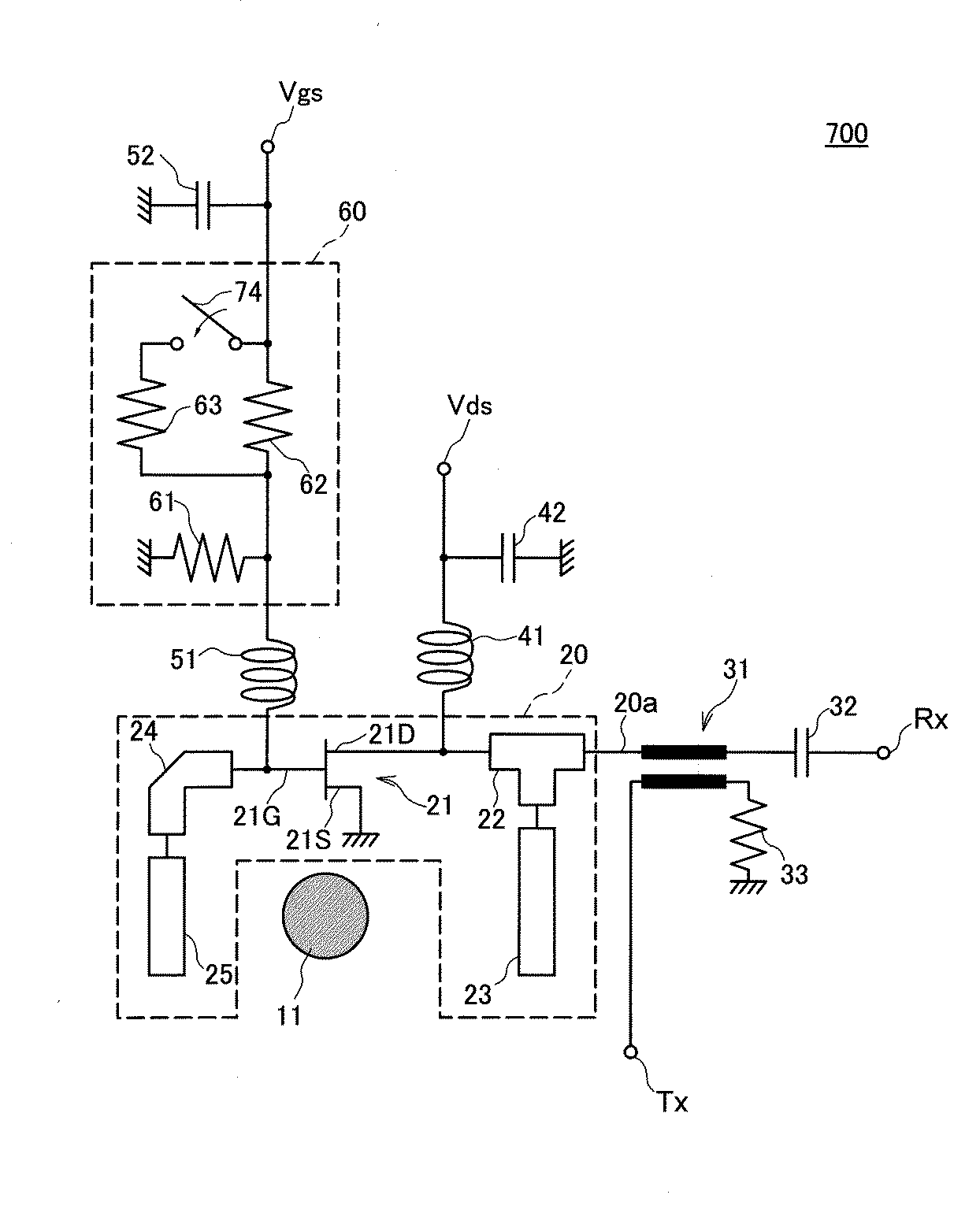
となる。
It becomes.
したがって、本実施形態においても、電圧VOFFによって駆動回路20が動作状態となり、且つ、電圧VONによって駆動回路20が動作停止状態となるよう、抵抗61〜63の抵抗値R61〜R63を設定すれば、スイッチ74のオン・オフによって発振動作の開始及び停止を極めて速やかに行うことが可能となる。
Therefore, in this embodiment, the
図8は、本発明の好ましい第6の実施形態による誘電体共振器装荷型発振回路800の回路図である。
FIG. 8 is a circuit diagram of a dielectric resonator loaded
図8に示すように、本実施形態による誘電体共振器装荷型発振回路800は、図1に示した誘電体共振器装荷型発振回路100に対し、接続点Aと制御端子Vcontとの間に接続されたコンデンサ81と、接続点Aとグランド電位との間に直列接続された抵抗82及びコンデンサ83を追加した構成を有している。その他の要素は、基本構成である図1に示した誘電体共振器装荷型発振回路100と同じであることから、同一の要素には同一の符号を付し、重複する説明は省略する。
As shown in FIG. 8, the dielectric resonator loaded
制御端子Vcontは、トランジスタ21のゲート21Gに与える電圧を変化させるための端子であり、一例として、誘電体共振器11を発振させる場合には1.7Vの電圧が与えられ、誘電体共振器11の発振を停止させる場合には0Vの電圧が与えられる。したがって、制御端子Vcontの電圧は、図9(a)に示すようなパルス状の波形となる。尚、コンデンサ81,83は直流カット用のコンデンサであり、抵抗82は制御端子Vcontの電圧変化時に生じるオーバーシュートやアンダーシュートを防止するための抵抗である。抵抗82の役割は抵抗61に兼用させることも可能であり、この場合には、抵抗82及びコンデンサ83は不要である。但し、抵抗82及びコンデンサ83を省略するためには、抵抗61,62の抵抗値をより低く設定する必要が生じ、これにより消費電力が増大する。
The control terminal Vcont is a terminal for changing the voltage applied to the
制御端子Vcontの電圧を変化させると、これに対応して接続点Aの電圧も図9(b)に示すように変化する。したがって、制御端子Vcontがハイレベル(例えば1.7V)である場合に駆動回路20が動作状態(例えば接続点A=−0.3V)となり、制御端子Vcontがローレベル(例えば0V)である場合に駆動回路20が動作停止状態(例えば接続点A=−2.0V)となるよう、抵抗61,62,82の抵抗値を設定すれば、制御端子Vcontの電圧変化に連動して、発振動作の開始及び停止を極めて速やかに行うことが可能となる。
When the voltage at the control terminal Vcont is changed, the voltage at the connection point A also changes as shown in FIG. 9B. Accordingly, when the control terminal Vcont is at a high level (eg, 1.7 V), the
また、本実施形態によれば、発振動作の開始及び停止を行うためのスイッチが不要となることから、回路構成をより簡素化することが可能となる。 In addition, according to the present embodiment, a switch for starting and stopping the oscillation operation is not necessary, so that the circuit configuration can be further simplified.
以上、本発明の好ましい実施形態について説明したが、本発明は、上記の実施形態に限定されることなく、本発明の主旨を逸脱しない範囲で種々の変更が可能であり、それらも本発明の範囲内に包含されるものであることはいうまでもない。 The preferred embodiments of the present invention have been described above, but the present invention is not limited to the above-described embodiments, and various modifications can be made without departing from the spirit of the present invention. Needless to say, it is included in the range.
例えば、上記各実施形態においては、駆動回路20に用いるトランジスタとしてHEMT型のトランジスタ21を用いているが、本発明においてこれは必須ではなく、バイポーラトランジスタなど、他の形式のトランジスタを用いても構わない。
For example, in each of the above embodiments, the
また、上記各実施形態においては、誘電体共振器11が信号線路23,25間に配置されているが、本発明において誘電体共振器11の配置がこれに限定されるものではなく、例えば、信号線路23,25の一方にのみ結合した構成としても構わない。
In each of the above embodiments, the
さらに、第1乃至第3の実施形態による誘電体共振器装荷型発振回路100,200,300ではトランジスタ21のドレイン21D側にスイッチを設け、第4及び第5の実施形態による誘電体共振器装荷型発振回路400,500ではトランジスタ21のゲート21G側にスイッチを設けているが、ドレイン21D側及びゲート21G側の両方にスイッチを設けても構わない。
Furthermore, in the dielectric resonator loaded
100,200,300,400,500,600,700,800 誘電体共振器装荷型発振回路
11 誘電体共振器
20 駆動回路
20a 駆動回路の出力端
21 トランジスタ
21G ゲート(制御電極)
21S ソース
21D ドレイン(被制御電極)
22〜25 信号線路
31 カプラ
32 コンデンサ
33 終端抵抗
41,51 チップビーズ
42,52,81,83 コンデンサ
60 分圧回路
61〜63,82 抵抗
71〜74 スイッチ
Rx 受信側ポート
Tx 送信側ポート
100, 200, 300, 400, 500, 600, 700, 800 Dielectric resonator loaded
22-25
Claims (3)
前記駆動回路は、制御電極と第1及び第2の被制御電極とを有するトランジスタと、該第1の被制御電極に接続された第1の信号線路と、該制御電極に接続された第2の信号線路とを含み、
前記誘電体共振器は前記第1の信号線路と前記第2の信号線路との間に配置され、
前記第1の被制御電極の出力は、前記第1の信号線路、前記誘電体共振器、及び前記第2の信号線路を介して前記制御電極に帰還し、
前記第1の被制御電極は、前記駆動回路が前記共振電圧を生成するために必要な第1の電圧が供給される第1の電源端子及び前記駆動回路に前記共振電圧の生成を停止させるグランド電位が供給される第2の電源端子に接続され、
前記制御電極は第3の電圧が供給される第3の電源端子に接続され、
前記第2の被制御電極はグランド電位に接続され、
前記誘電体共振器装荷型発振回路は、
前記第1の被制御電極と前記第1の電源端子との間に設けられた第1のスイッチと、
前記第1の被制御電極と前記第2の電源端子との間に設けられた第2のスイッチと、
をさらに備え、
前記第1及び第2のスイッチは排他的に導通することを特徴とする誘電体共振器装荷型発振回路。 A dielectric resonator loaded oscillation circuit comprising a dielectric resonator and a drive circuit for applying a resonance voltage to the dielectric resonator,
The drive circuit includes a transistor having a control electrode and first and second controlled electrodes, a first signal line connected to the first controlled electrode, and a second signal connected to the control electrode. Including signal lines ,
The dielectric resonator is disposed between the first signal line and the second signal line,
The output of the first controlled electrode is fed back to the control electrode via the first signal line, the dielectric resonator, and the second signal line,
The first controlled electrode includes a first power supply terminal to which a first voltage necessary for the drive circuit to generate the resonance voltage is supplied, and a ground for causing the drive circuit to stop generating the resonance voltage. Connected to a second power supply terminal to which a potential is supplied;
The control electrode is connected to a third power supply terminal to which a third voltage is supplied,
The second controlled electrode connected to the ground conductive position,
The dielectric resonator loaded oscillation circuit is:
A first switch provided between the first controlled electrode and the first power supply terminal;
A second switch provided between the first controlled electrode and the second power supply terminal;
Further comprising
The dielectric resonator loaded oscillation circuit, wherein the first and second switches are exclusively conductive.
Priority Applications (2)
| Application Number | Priority Date | Filing Date | Title |
|---|---|---|---|
| JP2006006716A JP4376231B2 (en) | 2005-03-08 | 2006-01-13 | Dielectric resonator loaded oscillation circuit and radar device using the same |
| US11/366,304 US7378915B2 (en) | 2005-03-08 | 2006-03-01 | Dielectric resonator oscillator and radar apparatus using the same |
Applications Claiming Priority (2)
| Application Number | Priority Date | Filing Date | Title |
|---|---|---|---|
| JP2005063285 | 2005-03-08 | ||
| JP2006006716A JP4376231B2 (en) | 2005-03-08 | 2006-01-13 | Dielectric resonator loaded oscillation circuit and radar device using the same |
Publications (2)
| Publication Number | Publication Date |
|---|---|
| JP2006287908A JP2006287908A (en) | 2006-10-19 |
| JP4376231B2 true JP4376231B2 (en) | 2009-12-02 |
Family
ID=36970192
Family Applications (1)
| Application Number | Title | Priority Date | Filing Date |
|---|---|---|---|
| JP2006006716A Expired - Fee Related JP4376231B2 (en) | 2005-03-08 | 2006-01-13 | Dielectric resonator loaded oscillation circuit and radar device using the same |
Country Status (2)
| Country | Link |
|---|---|
| US (1) | US7378915B2 (en) |
| JP (1) | JP4376231B2 (en) |
Families Citing this family (4)
| Publication number | Priority date | Publication date | Assignee | Title |
|---|---|---|---|---|
| ATE553531T1 (en) * | 2006-10-17 | 2012-04-15 | Mitsubishi Electric Corp | OSCILLATOR, TRANSMIT/RECEIVE DEVICE AND FREQUENCY SYNTHESIZER |
| CN101930269A (en) * | 2009-06-18 | 2010-12-29 | 鸿富锦精密工业(深圳)有限公司 | SATA (Serial Advanced Technology Attachment) control chip power supply circuit |
| TWI429195B (en) * | 2010-12-08 | 2014-03-01 | Ind Tech Res Inst | Power circuit and dc to dc converter thereof |
| JP2014212469A (en) * | 2013-04-19 | 2014-11-13 | 東京計器株式会社 | Microwave power oscillator and output control method |
Family Cites Families (5)
| Publication number | Priority date | Publication date | Assignee | Title |
|---|---|---|---|---|
| JP2947326B2 (en) | 1994-05-23 | 1999-09-13 | 三菱電機株式会社 | Interference prevention device |
| GB9510028D0 (en) * | 1995-05-18 | 1995-07-12 | Cambridge Ind Ltd | Local oscillator noise rejection circuit |
| JP3661573B2 (en) * | 2000-07-24 | 2005-06-15 | 株式会社村田製作所 | Voltage-controlled oscillator, voltage-controlled oscillator device, and radar device |
| JP3914401B2 (en) * | 2001-09-06 | 2007-05-16 | 株式会社日立製作所 | Oscillator, transmission / reception module, and radar apparatus |
| US6714089B2 (en) * | 2002-05-29 | 2004-03-30 | Xytrans, Inc. | High frequency signal source and method of generating same using dielectric resonator oscillator (DRO) circuit |
-
2006
- 2006-01-13 JP JP2006006716A patent/JP4376231B2/en not_active Expired - Fee Related
- 2006-03-01 US US11/366,304 patent/US7378915B2/en not_active Expired - Fee Related
Also Published As
| Publication number | Publication date |
|---|---|
| JP2006287908A (en) | 2006-10-19 |
| US20060202770A1 (en) | 2006-09-14 |
| US7378915B2 (en) | 2008-05-27 |
Similar Documents
| Publication | Publication Date | Title |
|---|---|---|
| US9862239B2 (en) | Antenna driving device | |
| US7283089B2 (en) | Radar system and car radar system | |
| US7521986B2 (en) | Switch element driver circuit and semiconductor device | |
| US8278834B2 (en) | PWM control method and device and light adjusting device | |
| JP4376231B2 (en) | Dielectric resonator loaded oscillation circuit and radar device using the same | |
| US7956728B2 (en) | Sound production controller | |
| JP2013083541A (en) | Rf pulse signal generating-switching circuit, rf pulse signal generating-circuit, and target detection device | |
| JP2006310287A (en) | Corrosion prevention method, corrosion prevention device, signal processor, and control unit | |
| EP2073386B1 (en) | Semiconductor output circuit | |
| CN109417349B (en) | Switching regulator control circuit, switching regulator and vehicle | |
| JP2001168695A (en) | Electronic driver circuit for electronic system and its method | |
| JP2000346927A (en) | Power supply device for radar | |
| JP6211360B2 (en) | Antenna drive device | |
| US11688937B2 (en) | Antenna device | |
| US6133653A (en) | Recirculating driver control circuit and method of operating the same | |
| WO2021246302A1 (en) | Switching power supply device, switch control device, vehicle-mounted apparatus, and vehicle | |
| US20240034151A1 (en) | Electronic control unit | |
| KR102300957B1 (en) | Apparatus and method for supplying a power source in power switching apparatus for RF high-power amplifier | |
| JP5121380B2 (en) | Pulse modulator | |
| US10211796B1 (en) | Common mode voltage ramping in Class-D amplifiers minimizing AM band emissions in passive keyless entry systems | |
| JP6262479B2 (en) | Antenna drive device | |
| JPH0712921A (en) | Pulse modulator for radar | |
| JP2001091638A (en) | Radar device | |
| CN117501572A (en) | Power supply control device, power supply control method, and program | |
| CN116232025A (en) | Switching power supply device |
Legal Events
| Date | Code | Title | Description |
|---|---|---|---|
| A977 | Report on retrieval |
Free format text: JAPANESE INTERMEDIATE CODE: A971007 Effective date: 20080627 |
|
| A131 | Notification of reasons for refusal |
Free format text: JAPANESE INTERMEDIATE CODE: A131 Effective date: 20080715 |
|
| A521 | Written amendment |
Free format text: JAPANESE INTERMEDIATE CODE: A523 Effective date: 20080911 |
|
| A131 | Notification of reasons for refusal |
Free format text: JAPANESE INTERMEDIATE CODE: A131 Effective date: 20090609 |
|
| A521 | Written amendment |
Free format text: JAPANESE INTERMEDIATE CODE: A523 Effective date: 20090730 |
|
| TRDD | Decision of grant or rejection written | ||
| A01 | Written decision to grant a patent or to grant a registration (utility model) |
Free format text: JAPANESE INTERMEDIATE CODE: A01 Effective date: 20090908 |
|
| A01 | Written decision to grant a patent or to grant a registration (utility model) |
Free format text: JAPANESE INTERMEDIATE CODE: A01 |
|
| A61 | First payment of annual fees (during grant procedure) |
Free format text: JAPANESE INTERMEDIATE CODE: A61 Effective date: 20090908 |
|
| R150 | Certificate of patent or registration of utility model |
Free format text: JAPANESE INTERMEDIATE CODE: R150 |
|
| FPAY | Renewal fee payment (event date is renewal date of database) |
Free format text: PAYMENT UNTIL: 20120918 Year of fee payment: 3 |
|
| FPAY | Renewal fee payment (event date is renewal date of database) |
Free format text: PAYMENT UNTIL: 20130918 Year of fee payment: 4 |
|
| LAPS | Cancellation because of no payment of annual fees |