JP4372845B2 - Power transformer / inductor - Google Patents
Power transformer / inductor Download PDFInfo
- Publication number
- JP4372845B2 JP4372845B2 JP53279698A JP53279698A JP4372845B2 JP 4372845 B2 JP4372845 B2 JP 4372845B2 JP 53279698 A JP53279698 A JP 53279698A JP 53279698 A JP53279698 A JP 53279698A JP 4372845 B2 JP4372845 B2 JP 4372845B2
- Authority
- JP
- Japan
- Prior art keywords
- power transformer
- semiconductor layer
- inductor
- winding
- ground
- Prior art date
- Legal status (The legal status is an assumption and is not a legal conclusion. Google has not performed a legal analysis and makes no representation as to the accuracy of the status listed.)
- Expired - Fee Related
Links
Images


Classifications
-
- H—ELECTRICITY
- H01—ELECTRIC ELEMENTS
- H01F—MAGNETS; INDUCTANCES; TRANSFORMERS; SELECTION OF MATERIALS FOR THEIR MAGNETIC PROPERTIES
- H01F27/00—Details of transformers or inductances, in general
- H01F27/34—Special means for preventing or reducing unwanted electric or magnetic effects, e.g. no-load losses, reactive currents, harmonics, oscillations, leakage fields
-
- H—ELECTRICITY
- H01—ELECTRIC ELEMENTS
- H01F—MAGNETS; INDUCTANCES; TRANSFORMERS; SELECTION OF MATERIALS FOR THEIR MAGNETIC PROPERTIES
- H01F27/00—Details of transformers or inductances, in general
- H01F27/28—Coils; Windings; Conductive connections
- H01F27/2823—Wires
- H01F27/2828—Construction of conductive connections, of leads
-
- H—ELECTRICITY
- H01—ELECTRIC ELEMENTS
- H01F—MAGNETS; INDUCTANCES; TRANSFORMERS; SELECTION OF MATERIALS FOR THEIR MAGNETIC PROPERTIES
- H01F27/00—Details of transformers or inductances, in general
- H01F27/28—Coils; Windings; Conductive connections
- H01F27/288—Shielding
-
- Y—GENERAL TAGGING OF NEW TECHNOLOGICAL DEVELOPMENTS; GENERAL TAGGING OF CROSS-SECTIONAL TECHNOLOGIES SPANNING OVER SEVERAL SECTIONS OF THE IPC; TECHNICAL SUBJECTS COVERED BY FORMER USPC CROSS-REFERENCE ART COLLECTIONS [XRACs] AND DIGESTS
- Y10—TECHNICAL SUBJECTS COVERED BY FORMER USPC
- Y10S—TECHNICAL SUBJECTS COVERED BY FORMER USPC CROSS-REFERENCE ART COLLECTIONS [XRACs] AND DIGESTS
- Y10S174/00—Electricity: conductors and insulators
- Y10S174/13—High voltage cable, e.g. above 10kv, corona prevention
Abstract
Description
技術分野
本発明は電力変圧器/誘導器に関する。
あらゆる電気エネルギーの伝達および配電において、変圧器は、通常は異なる電圧レベルを有する2つ以上の電気系間の交換を可能にするために使用される。変圧器は、VA領域から1000MVA領域までの電力に使用することができる。電圧領域は、今日使用されている最高伝達電圧までの範囲を有する。電磁誘導は、電気系間のエネルギー伝達に使用される。
誘導器も、例えば位相補償およびフィルタリングなどで電気エネルギーを伝達するのに基本的な構成要素である。
本発明に関する変圧器/誘導器は、数百kVAから1000MVA超までの定格出力および3〜4kVから非常に高い送電電圧までの定格電圧を有する、いわゆる電力変圧器/誘導器に属する。
背景技術
概して、電力変圧器の主な目的は、大抵は同じ周波数で電圧が異なる2つ以上の電気系間で電気エネルギーを交換できるようにすることである。
従来通りの電力変圧器/誘導器は、例えばスウェーデンのThe Royal Institute of Technologyが1996年に出版したFredrik Gustavson著の「Electriska Maskiner」の3−6から3−12ページに記載されている。
従来通りの電力変圧器/誘導器は変圧器芯を備え、これは以下では芯と呼び、積層状で共通方向の、通常はシリコン鉄の薄板で形成される。芯は、ヨークで接続された幾つかの芯脚で構成される。芯脚の周囲には幾つかの巻線が設けられ、これは通常、1次、2次および調整巻線と呼ばれる。電力変圧器では、これらの巻線は、実際には常に同心円形状に配置され、芯脚の長さに沿って分布する。
他のタイプの芯構造は、例えばいわゆる外鉄型変圧器またはリング芯変圧器で生じることがある。芯変圧器に関する例が、ドイツ特許第40414号で検討されている。芯は、前記指向性薄板などの従来通りの磁化可能な材料およびフェライト、アモルファス材料、ワイヤ撚り線または金属テープなどの他の磁化可能な材料で構成することができる。磁化可能な芯は、周知のように、誘導器には不必要である。
上述した巻線は、直列に接続された1つまたは幾つかのコイルで構成され、そのコイルは直列に接続された幾つかの巻を有する。単一コイルの巻は、通常、残りのコイルから物理的に分離された幾何学的な連続単位を構成する。
米国特許第5 036 165号で、熱分解された半導体グラスファイバの内外層で絶縁された導体が知られている。例えば米国特許第5 066 881号に記載されているように、このように絶縁したダイナモエレクトリック機械に導体を設けることも知られ、ここでは熱分解した半導体グラスファイバ層が、導体を形成する2本の平行な棒と接触し、固定子スロット内の絶縁体が熱分解半導体グラスファイバの外層に囲まれている。熱分解されたグラスファイバ材料が適切とされるのは、含浸処理の後にも抵抗率を維持するからである。
部分的にコイル/巻線の内部にあり、部分的にコイル/巻線間にある絶縁システムおよび残りの金属部品は、通常、固体またはワニス系絶縁体の形態であり、外側にある絶縁システムは、固体セルロース絶縁体、流体絶縁体の形態、および場合によっては気体の形態でもある。絶縁体および場合によっては嵩張った部品を有する巻線は、このように、変圧器に属する能動電磁気部品中またはその周囲に発生する高強度の電界に影響される大きい体積になる。発生する誘電場の強度を予め求め、放電の危険が最小になるよう寸法を決定するためには、絶縁材の特性を詳細に知る必要がある。絶縁特性を変化させたり低下させたりしない周囲環境を達成することが重要である。
従来通りの高電圧電力変圧器/誘導器に現在主に使用されている外部絶縁システムは、固体絶縁体としてのセルロース材料および流体絶縁体としての変圧器オイルで構成される。変圧器オイルは、いわゆる鉱物油をベースとする。
従来通りの絶縁システムは、例えばスウェーデンのThe Royal Institute of Technologyが1996年に出版したFredrik Gustavson著の「Electriska Maskiner」の3−6から3−12ページに記載されている。
また、従来通りの絶縁システムは、構築するのが比較的複雑であり、そのうえ絶縁システムの優れた絶縁特性を利用するために、製造中に特別な措置を執る必要がある。システムは水分含有率が低くなければならず、絶縁システムの固体相は、気体ポケットの危険性が最小になるよう、周囲のオイルを十分含浸する必要がある。製造中に、下げてタンクに入れる前に、巻線付きの完全な芯で乾燥プロセスを実行する。芯を下げてタンクを密封した後、特殊な真空処理によってタンクの空気を全部空にしてから、オイルを充填する。このプロセスは、全体の製造プロセスから見て比較的時間がかかり、そのうえ作業場の資源を大量に使用する。
変圧器を囲むタンクは、完全な真空に耐えられるような方法で構築しなければならない。というのは、プロセスで、ほぼ絶対真空まで全てのガスを抜く必要があり、これには過剰な材料を消費し、製造時間がかかるからである。
さらに、設備は、検査のために変圧器を開くたびに、真空処理を繰り返す必要がある。
発明の概要
本発明によると、電力変圧器/誘導器は、大抵の場合は様々な幾何学的形状を有することができる磁化可能な芯の周囲に配置される、少なくとも1つの巻線を備える。以下の明細書を単純化するため、以下では「巻線」という用語を使用する。巻線は、固体絶縁体を有する高圧ケーブルで構成される。ケーブルは、中心に配置された少なくとも1つの電気導体を有する。導体の周囲には第1半導体層が配置され、半導体層の周囲には固体絶縁層が配置され、固体絶縁層の周囲には第2外部半導体層が配置される。
このようなケーブルを使用することは、高い電気応力がかかる変圧器/誘導器の領域が、ケーブルの固体絶縁体に限定されることを示唆する。変圧器/誘導器の残りの部分は、高圧に関して、あまり極端でない電界強度にしか曝されない。さらに、このようなケーブルを使用すると、本発明の背景の項で述べた幾つかの問題領域がなくなる。したがって、絶縁手段や冷却剤のタンクが不必要である。絶縁材も、全体として非常に単純になる。製造する時間も、従来通りの電力変圧器/誘導器と比較して非常に短くなる。巻線は別個に製造することができ、電力変圧器/誘導器を現場で組み立ててもよい。
しかし、このようなケーブルを使用すると、解決しなければならない新しい問題が生じる。通常の動作電圧中および過渡状態進行中の両方で生じる電気応力が、主にケーブルの固体絶縁体にのみ負荷をかけるよう、ケーブルの両端またはその近傍でのみ、第2半導体層を直接接地しなければならないのである。半導体層およびその直接接地部はともに、操作中に電流が誘導される閉回路を形成する。層の抵抗率は、層中に発生する抵抗損が無視できるほど十分に大きくなければならない。
この磁気誘導電流以外に、容量性電流がケーブルの直接接地した両端を通して層に流れ込む。層の抵抗率が大きすぎると、容量性電流が非常に限られるので、交番応力中に巻線の固体絶縁体以外の電力変圧器/誘導器の領域に電気応力がかかる程度まで、層の部分の電位が接地電位から異なってもよい。半導体層の幾つかの点、好ましくは巻線の巻ごとに1カ所を直接接地することにより、層の導電性が十分高ければ、外層全体が接地電位にあり、上記の問題がなくなることが確保される。
このように外層の巻ごとに1カ所接地することは、接地点が巻線の母線上にあり、巻線の軸長に沿った点が、その後に共通接地電位に接続される導電性接地トラックに電気的に直接接続されるような方法で実行される。
極端な場合、巻線は非常に急速な過渡的過電圧に曝されることがあるので、外部半導体層の部分が、ケーブルの絶縁体以外の電力変圧器の区域が望ましくない電気応力を受けるような電位を有することになる。このような状況を防止するため、例えば火花ギャップ、ファントロン、ツェーナー・ダイオードまたはバリスターなどの幾つかの非線形エレメントを、巻線の巻ごとに外部半導体層とアース間に接続する。また、コンデンサを外部半導体層とアースとの間に接続することにより、非線形電気応力の上昇を防止することができる。コンデンサは50Hzでも電圧を低下させる。この接地原理を、以下では「間接接地」と呼ぶ。
本発明による電力変圧器/誘導器では、第2半導体層を各巻線の両端で直接接地し、両端間の少なくとも1カ所で間接接地する。
個々に接地された接地トラックは、以下のいずれかを介してアースに接続される。
1.火花ギャップまたはファントロンなどの非線形エレメント。
2.コンデンサに平行な非線形エレメント。
3.コンデンサ。
または3つの選択肢全部の組合せ。
本発明による電力変圧器/誘導器では、巻線はXLPEケーブルのように、現在配電に使用されているタイプの固体押出し絶縁体を有するケーブル、またはEPA絶縁体を有するケーブルで構成することが好ましい。このようなケーブルは可撓性であり、これはこの状況では重要な特性である。というのは、本発明による装置のテクノロジーが、主に、巻線が組立中に曲げられるケーブルから形成される巻線システムをベースとするからである。XLPEケーブルの可撓性は、通常、直径30mmのケーブルの場合は約20cmの曲率半径に、直径80mmのケーブルの場合は約65cmの曲率半径に相当する。本出願では、「可撓性」という用語は、巻線がケーブル直径の4倍、好ましくはケーブル直径の8倍から12倍のオーダーで曲率半径まで撓むことができることを示す。
本発明の巻線は、使用中に曲げられ、熱応力がかかった場合でも、その特性を維持するよう構築される。ケーブルの層が、この状況で互いに対する付着力を保持することがきわめて重要である。ここでは層の材料特性、特にその弾性および相対熱膨張率が非常に重要である。例えばXLPEケーブルでは、絶縁層が架橋低密度ポリエチレンで構成され、半導体層が、煤および金属粒子を混合したポリエチレンで構成される。温度変動の結果生じる体積の変化は、ケーブルの半径の変化として完全に吸収され、これらの材料は弾性に対して層の熱膨張係数の差が比較的わずかであるので、層間の付着が失われることなく半径方向に膨張することができる。
上述した材料の組合せは、例証にすぎないと考えられる。規定された状態を満たす他の組合せ、および半導性である、つまり抵抗率が10-1〜10-6Ωcm、例えば1〜500Ωcmまたは10〜200Ωcmの範囲である状態も、当然、本発明の範囲に入る。
絶縁層は、例えば低密度ポリエチレン(LDPE)、高密度ポリエチレン(HDPE)、ポリプロピレン(PP)、ポリブチレン(PB)、ポリメチルペンタン(PMP)などの固体熱可塑性材料、架橋ポリエチレン(XLPC)などの架橋材料、またはエチレンプロピレンゴム(EPR)またはシリコンゴムなどのゴムで構成することができる。
内部および外部半導体層は、同じ基本的材料でもよいが、煤や金属粉などの導電材料の粒子が混入される。
これらの材料の機械的性質、特にその熱膨張係数は、煤または金属粉が混入されているか否かには、少なくとも本発明により必要な導電性を達成するのに必要な割合では、それほど影響されない。したがって、絶縁層および半導体層は、ほぼ同じ熱膨張係数を有する。
エチレン酢酸ビニル共重合体/ニトリル・ゴム、ブチル・グラフト・ポリエチレン、エチレン酢酸ブチル共重合体およびエチレンエチルアクリレート共重合体も、半導体層の適切な重合体を構成することができる。
種々の層のベースとして異なるタイプの材料を使用する場合でも、その熱膨張係数がほぼ同じであることが望ましい。上に挙げた材料の組合せは、これに当てはまる。
上に挙げた材料は弾性が比較的良好で、弾性率がE<500MPa、好ましくは<200MPaである。弾性率は、層の材料の熱膨張係数にわずかな差があっても、ひび割れや他の損傷が現れず、層が互いから剥離しないよう、半径方向の弾性率に吸収されるのに十分である。層の材料は弾性であり、層間の付着力は、少なくとも最も弱い材料と同じ大きさである。
2つの半導体層の導電性は、各層に沿って電位をほぼ等しくするのに十分である。外部半導体層の導電性は、ケーブル内に電界を含むのに十分なほど大きいが、層の縦方向に誘導された電流によって有意の損失が生じることがないほど十分に小さい。
したがって、2つの半導体層はそれぞれ、基本的に1つの等電位表面を備え、これらの層はその間に電界をほぼ封じ込める。
言うまでもなく、絶縁層内に1つまたは複数の追加の半導体層を配置するのは差し支えない。
上記およびその他の本発明の有利な実施形態は、請求の範囲の従属項に記載される。
次に、本発明について、添付図面類を参照しながら、好ましい実施形態に関する以下の記述で、さらに詳細に述べる。
【図面の簡単な説明】
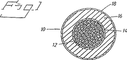
図1は、高圧ケーブルの断面図を示す。
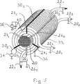
図2は、本発明の第1の実施形態により巻線の巻ごとに3つの間接接地点がある巻線の斜視図を示す。
図3は、本発明の第2の実施形態により巻線の巻ごとに1つの直接接地点および2つの間接接地点がある巻線の斜視図を示す。
図4は、本発明の第3の実施形態により巻線の巻ごとに1つの直接接地点および2つの間接接地点がある、巻線の斜視図を示す。
図5は、本発明の第4の実施形態により巻線の巻ごとに1つの直接接地点および2つの間接接地点がある、巻線の斜視図を示す。
本発明の実施形態の詳細な説明
図1は、従来から電気エネルギーの伝達に使用されている高圧ケーブル10の断面図を示す。図示の高圧ケーブルは、例えば、標準のXLPEケーブル145kVでもよいが、外被と遮壁はない。高圧ケーブル10は電気導体を備え、これは例えば銅(Cu)の円形断面の1本または数本の撚り線12を備えることができる。これらの撚り線12は、高圧ケーブル10の中心に配置される。撚り線12の周囲には第1半導体層14が配置される。第1半導体層14の周囲には、例えばXLPE絶縁体の第1絶縁層16が配置される。第1絶縁層16の周囲には第2半導体層18が配置される。
図1に示す高圧ケーブル10は、導体面積が80から3000mm2、ケーブル外径が20から250mmで製造される。
図2は、本発明の第1の実施形態により巻線の巻ごとに3つの間接接地点がある巻線の斜視図を示す。図2は、電力変圧器または誘導器の中にあり数字20で指定される芯脚を示す。2本の巻線221および222が、図1に示す高圧ケーブル(10)から形成された芯脚20の周囲に配置される。巻線221および222を固定するため、この場合は巻線の巻ごとに6つの半径方向に配置されたスペーサ部材241、242、243、244、245、246がある。図2に示すように、外部半導体層は巻線221、222ごとに両端261、262、281、282で接地される。スペーサ部材241、243、245は、黒で強調されているが、この場合は巻線の巻ごとに3つの間接接地点を獲得するのに使用される。巻線222の周囲で、かつ巻線222の軸方向の長さに沿って、スペーサ部材241が第1設置要素301に直接接続され、スペーサ部材243が第2接地要素302に直接接続され、スペーサ部材245が第3接地要素303に直接接続される。接地要素301、302、303は、例えば接地トラック301〜303の形態でよい。図2で示すように、接地点は巻線の母線上にある。接地要素301〜303はそれぞれ1つずつ、そのコンデンサ321、322、323を介してアースに接続されるという点で、直接接地される。この方法で間接的に接地することにより、望ましくない電気応力の発生を防止することができる。
図3は、本発明の第2の実施形態により巻線の巻ごとに1つの直接接地点および2つの間接接地点がある巻線の斜視図を示す。図2および図3では、図をさらに明瞭にするために、同じ部品には同じ数字が割り当てられている。この場合も、図1に示す高圧ケーブル10から形成された2本の巻線221および222は、芯脚20の周囲に配置される。巻線221、222は、巻線の巻ごとに6つのスペーサ部材241、242、243、244、245、246によって固定される。各巻線221および222の両端261、262、281、282で、第2半導体層(図1と比較すると)は図2に従って接地される。スペーサ部材241、243、245は、黒で印されているが、この場合は巻線の巻ごとに1つの直接接地点および2つの間接接地点を獲得するために使用される。図2で示したのと同じ方法で、スペーサ部材241は第1接地要素301に直接接続され、スペーサ部材243は第2接地要素302に直接接続され、スペーサ部材245は第3接地要素303に直接接続される。図3に示すように、接地要素301はアース36に直接接続され、接地要素302、303は間接的に接地される。接地要素303は、コンデンサ32を介してアースに直列に接続されるという点で、間接的に接地される。接地要素302は、火花ギャップ34を介してアースに直列に接続されるという点で、間接的に接地される。火花ギャップは非線形素子、つまり非線形電圧電流特性を有する素子の一例である。
図4は、本発明の第3の実施形態により巻線の巻ごとに1つの直接接地点および2つの間接接地点がある巻線の斜視図を示す。図2から図4では、図をさらに明瞭にするために、同じ部品には同じ数字が割り当てられている。図4は、図3で示したのと同じ方法で配置された巻線221、222、芯脚20、スペーサ部材241、242、243、244、245、246および接地要素301、302、303を示し、したがってここではこれ以上詳細には説明しない。接地要素301はアースに直接接続され、接地要素302、303は間接的に接地される。接地要素302、303は、そのコンデンサを介して直列に接続されるという点で、間接的に接地される。
図5は、本発明の第4の実施形態により、巻線の巻ごとに1つの直接接地点および2つの間接接地点がある巻線の斜視図を示す。図5は、図3および図4で示したのと同じ方法で配置された巻線221、222、芯脚20、スペーサ部材241、242、243、244、245、246および接地要素301、302、303を示し、したがってここではこれ以上詳細には説明しない。接地要素301はアース36に直接接続され、接地要素302、303は間接的に接地される。接地要素302は、火花ギャップを介してアースに直列に接続されるという点で、間接的に接地される。接地要素303は、コンデンサ40に並列接続された火花ギャップ38を備える回路を介してアースに直列に接続されるという点で、間接的に接地される。
本発明の上記で示した実施形態の火花ギャップは、例示的に示したのみである。
上に示した図の電力変圧器/誘導器は、磁化可能な芯を備える。しかし、電力変圧器/誘導器は磁鉄芯なしでも設計できることを理解されたい。
本発明は、添付請求の範囲の枠内で幾つかの変形が可能であるので、示した実施形態に限定されるものではない。 TECHNICAL FIELD The present invention relates to power transformers / inductors.
In any electrical energy transfer and distribution, transformers are used to allow exchange between two or more electrical systems, usually having different voltage levels. The transformer can be used for power from the VA region to the 1000 MVA region. The voltage domain has a range up to the highest transmission voltage used today. Electromagnetic induction is used for energy transfer between electrical systems.
Inductors are also fundamental components for transferring electrical energy, for example, by phase compensation and filtering.
The transformer / inductor according to the invention belongs to a so-called power transformer / inductor with a rated output from several hundred kVA to more than 1000 MVA and a rated voltage from 3-4 kV to a very high transmission voltage.
BACKGROUND ART In general, the main purpose of a power transformer is to allow electrical energy to be exchanged between two or more electrical systems that are often at the same frequency and differing in voltage.
Conventional power transformers / inductors are described, for example, on pages 3-6 to 3-12 of “Electriska Maskiner” by Fredrik Gustavson, published in 1996 by The Royal Institute of Technology, Sweden.
A conventional power transformer / inductor comprises a transformer core, hereinafter referred to as the core, which is formed of a laminate and a common orientation, usually a thin sheet of silicon iron. The core is composed of several core legs connected by a yoke. Several windings are provided around the core leg, which are usually referred to as primary, secondary and adjustment windings. In power transformers, these windings are actually always arranged concentrically and distributed along the length of the core leg.
Other types of core structures may occur, for example, in so-called outer iron type transformers or ring core transformers. An example of a core transformer is discussed in German Patent No. 40414. The core can be composed of conventional magnetizable materials such as the directional sheet and other magnetizable materials such as ferrite, amorphous material, wire strands or metal tape. A magnetizable core is not necessary for the inductor, as is well known.
The winding described above is composed of one or several coils connected in series, which coil has several turns connected in series. A single coil turn usually constitutes a geometric continuous unit physically separated from the remaining coils.
In U.S. Pat. No. 5,036,165, a conductor is known which is insulated with the inner and outer layers of a pyrolyzed semiconductor glass fiber. For example, as described in US Pat. No. 5,066,881, it is also known to provide a conductor in such an insulated dynamo-electric machine, where two pyrolytic semiconductor glass fiber layers form the conductor. The insulator in the stator slot is surrounded by the outer layer of pyrolytic semiconductor glass fiber. Pyrolyzed glass fiber materials are suitable because they maintain resistivity after the impregnation process.
The insulation system and the remaining metal parts that are partly inside the coil / winding and partly between the coil / winding are usually in the form of a solid or varnish-based insulator, and the insulation system that is outside is In the form of a solid cellulose insulator, a fluid insulator, and in some cases a gas. Windings with insulators and possibly bulky parts thus have a large volume that is affected by high-intensity electric fields generated in or around the active electromagnetic parts belonging to the transformer. In order to determine the strength of the generated dielectric field in advance and determine the dimensions so as to minimize the risk of discharge, it is necessary to know the characteristics of the insulating material in detail. It is important to achieve an ambient environment that does not change or degrade the insulation properties.
The external insulation system currently used primarily in conventional high voltage power transformers / inductors consists of cellulosic material as a solid insulator and transformer oil as a fluid insulator. Transformer oil is based on so-called mineral oil.
Conventional insulation systems are described, for example, on pages 3-6 to 3-12 of “Electriska Maskiner” by Fredrik Gustavson, published in 1996 by The Royal Institute of Technology, Sweden.
In addition, conventional insulation systems are relatively complex to construct, and special measures need to be taken during manufacture to take advantage of the superior insulation properties of the insulation system. The system must have a low moisture content, and the solid phase of the insulation system must be sufficiently impregnated with the surrounding oil to minimize the risk of gas pockets. During manufacturing, the drying process is carried out with a complete core with windings before being lowered into the tank. After the wick is lowered and the tank is sealed, all the air in the tank is emptied by a special vacuum treatment and then filled with oil. This process is relatively time consuming in view of the overall manufacturing process and also uses a large amount of workplace resources.
The tank surrounding the transformer must be constructed in such a way that it can withstand a complete vacuum. This is because the process requires that all gases be vented to near absolute vacuum, which consumes excess material and takes manufacturing time.
In addition, the facility must repeat the vacuum process every time the transformer is opened for inspection.
SUMMARY OF THE INVENTION According to the present invention, a power transformer / inductor is at least one winding disposed around a magnetizable core that can often have various geometric shapes. With lines. To simplify the following specification, the term “winding” will be used in the following. The winding is composed of a high voltage cable having a solid insulator. The cable has at least one electrical conductor disposed in the center. A first semiconductor layer is disposed around the conductor, a solid insulating layer is disposed around the semiconductor layer, and a second external semiconductor layer is disposed around the solid insulating layer.
Using such a cable suggests that the area of the transformer / inductor that is subject to high electrical stress is limited to the solid insulation of the cable. The rest of the transformer / inductor is only exposed to less extreme field strengths with respect to high voltage. Furthermore, the use of such a cable eliminates some of the problem areas mentioned in the background section of the present invention. Therefore, no insulating means or coolant tank is required. The insulation is also very simple as a whole. Manufacturing time is also very short compared to conventional power transformers / inductors. The windings can be manufactured separately and the power transformer / inductor may be assembled on site.
However, the use of such cables creates new problems that must be solved. The second semiconductor layer must be grounded directly only at or near the ends of the cable so that electrical stresses that occur both during normal operating voltages and during transients are primarily loaded only on the cable's solid insulation. It must be done. The semiconductor layer and its direct ground together form a closed circuit in which current is induced during operation. The resistivity of the layer must be large enough that the resistance loss that occurs in the layer is negligible.
In addition to this magnetic induction current, a capacitive current flows into the layer through the directly grounded ends of the cable. If the resistivity of the layer is too high, the capacitive current will be very limited, so the layer part will not be subjected to electrical stress in the area of the power transformer / inductor other than the winding solid insulator during the alternating stress. May be different from the ground potential. Direct grounding at several points in the semiconductor layer, preferably at every turn of the winding, ensures that the entire outer layer is at ground potential if the layer is sufficiently conductive, eliminating the above problems. Is done.
Thus, grounding at one place for each winding of the outer layer means that the grounding point is on the winding bus and the point along the axial length of the winding is connected to the common ground potential thereafter. It is executed in such a way that it is electrically connected directly to.
In extreme cases, the windings may be exposed to very rapid transient overvoltages, so that parts of the outer semiconductor layer are subject to undesirable electrical stress in areas of the power transformer other than the cable insulation. Will have a potential. In order to prevent this situation, several non-linear elements such as spark gaps, fantrons, Zener diodes or varistors are connected between the external semiconductor layer and ground for every turn of the winding. Further, by connecting the capacitor between the external semiconductor layer and the ground, it is possible to prevent an increase in nonlinear electrical stress. The capacitor reduces the voltage even at 50 Hz. This grounding principle is hereinafter referred to as “indirect grounding”.
In the power transformer / inductor according to the present invention, the second semiconductor layer is directly grounded at both ends of each winding and indirectly grounded at at least one point between both ends.
Individually grounded ground tracks are connected to ground through either:
1. Non-linear elements such as spark gaps or fantrons.
2. Non-linear element parallel to the capacitor.
3. Capacitor.
Or a combination of all three options.
In the power transformer / inductor according to the invention, the windings are preferably composed of cables with solid extruded insulation of the type currently used for power distribution, such as XLPE cables, or cables with EPA insulation. . Such cables are flexible, which is an important property in this situation. This is because the technology of the device according to the invention is mainly based on a winding system in which the windings are formed from cables that are bent during assembly. The flexibility of an XLPE cable typically corresponds to a radius of curvature of about 20 cm for a 30 mm diameter cable and about 65 cm for a 80 mm diameter cable. In the present application, the term “flexible” indicates that the winding can bend to a radius of curvature in the order of 4 times the cable diameter, preferably 8 to 12 times the cable diameter.
The windings of the present invention are constructed to maintain their properties even when bent during use and subjected to thermal stress. It is critical that the cable layers maintain adhesion to each other in this situation. Here, the material properties of the layer, in particular its elasticity and relative coefficient of thermal expansion, are very important. For example, in the XLPE cable, the insulating layer is made of cross-linked low-density polyethylene, and the semiconductor layer is made of polyethylene in which cocoons and metal particles are mixed. The change in volume resulting from temperature fluctuations is completely absorbed as a change in cable radius, and the adhesion between the layers is lost because these materials have a relatively small difference in thermal expansion coefficient of the layers relative to elasticity. It can expand radially without.
The material combinations described above are considered to be examples only. Other combinations that meet the specified conditions, and those that are semiconducting, that is, having a resistivity in the range of 10 −1 to 10 −6 Ωcm, such as 1 to 500 Ωcm or 10 to 200 Ωcm, are naturally also included in the present invention. Enter the range.
The insulating layer may be a solid thermoplastic material such as low-density polyethylene (LDPE), high-density polyethylene (HDPE), polypropylene (PP), polybutylene (PB), or polymethylpentane (PMP), or cross-linked polyethylene (XLPC). It can be composed of a material or rubber such as ethylene propylene rubber (EPR) or silicon rubber.
The inner and outer semiconductor layers may be the same basic material, but are mixed with particles of conductive material such as soot and metal powder.
The mechanical properties of these materials, in particular their coefficient of thermal expansion, are not significantly affected by the presence of soot or metal powders, at least in the proportions necessary to achieve the conductivity required by the present invention. . Therefore, the insulating layer and the semiconductor layer have substantially the same thermal expansion coefficient.
Ethylene vinyl acetate copolymer / nitrile rubber, butyl graft polyethylene, ethylene butyl acetate copolymer and ethylene ethyl acrylate copolymer can also constitute suitable polymers for the semiconductor layer.
Even when different types of materials are used as the basis for the various layers, it is desirable that their coefficients of thermal expansion be approximately the same. This is the case with the material combinations listed above.
The materials listed above have relatively good elasticity and an elastic modulus of E <500 MPa, preferably <200 MPa. The elastic modulus is sufficient to be absorbed by the radial elastic modulus so that even if there is a slight difference in the coefficient of thermal expansion of the layer material, no cracks or other damage will appear and the layers will not delaminate from each other. is there. The material of the layers is elastic and the adhesion between the layers is at least as large as the weakest material.
The conductivity of the two semiconductor layers is sufficient to make the potential approximately equal along each layer. The conductivity of the outer semiconductor layer is large enough to contain an electric field in the cable, but small enough that no significant loss is caused by the current induced in the longitudinal direction of the layer.
Thus, each of the two semiconductor layers basically comprises one equipotential surface, and these layers substantially contain the electric field therebetween.
Needless to say, one or more additional semiconductor layers may be disposed in the insulating layer.
These and other advantageous embodiments of the invention are described in the dependent claims.
The present invention will now be described in further detail in the following description of preferred embodiments with reference to the accompanying drawings.
[Brief description of the drawings]
FIG. 1 shows a cross-sectional view of a high-voltage cable.
FIG. 2 shows a perspective view of a winding with three indirect ground points for each winding turn according to the first embodiment of the present invention.
FIG. 3 shows a perspective view of a winding with one direct ground point and two indirect ground points for each winding turn according to a second embodiment of the present invention.
FIG. 4 shows a perspective view of a winding with one direct ground point and two indirect ground points for each winding turn according to a third embodiment of the present invention.
FIG. 5 shows a perspective view of a winding with one direct ground point and two indirect ground points for each winding turn according to a fourth embodiment of the present invention.
Detailed Description of Embodiments of the Invention FIG. 1 shows a cross-sectional view of a
The high-
FIG. 2 shows a perspective view of a winding with three indirect ground points for each winding turn according to the first embodiment of the present invention. FIG. 2 shows a core leg that is in the power transformer or inductor and designated by the numeral 20. Two windings 22 1 and 22 2 are arranged around the
FIG. 3 shows a perspective view of a winding with one direct ground point and two indirect ground points for each winding turn according to a second embodiment of the present invention. 2 and 3, the same parts have been assigned the same numbers for the sake of clarity. Also in this case, the two windings 22 1 and 22 2 formed from the high-
FIG. 4 shows a perspective view of a winding with one direct ground point and two indirect ground points for each winding turn according to a third embodiment of the present invention. In FIGS. 2-4, the same numbers are assigned to the same parts to further clarify the figures. FIG. 4 shows windings 22 1 , 22 2 ,
FIG. 5 shows a perspective view of a winding with one direct ground point and two indirect ground points for each winding turn, according to a fourth embodiment of the present invention. FIG. 5 shows windings 22 1 , 22 2 ,
The spark gap of the above-described embodiment of the present invention is only shown by way of example.
The power transformer / inductor of the diagram shown above comprises a magnetizable core. However, it should be understood that a power transformer / inductor can be designed without a magnetic core.
The invention is not limited to the embodiments shown, since several modifications are possible within the scope of the appended claims.
Claims (16)
Applications Claiming Priority (5)
| Application Number | Priority Date | Filing Date | Title |
|---|---|---|---|
| SE9700337-0 | 1997-02-03 | ||
| SE9700337A SE508768C2 (en) | 1997-02-03 | 1997-02-03 | Power transformer-inductor winding |
| SE9704413-5 | 1997-11-28 | ||
| SE9704413A SE9704413D0 (en) | 1997-02-03 | 1997-11-28 | A power transformer / reactor |
| PCT/SE1998/000154 WO1998034246A1 (en) | 1997-02-03 | 1998-02-02 | Power transformer/inductor |
Publications (3)
| Publication Number | Publication Date |
|---|---|
| JP2001509958A JP2001509958A (en) | 2001-07-24 |
| JP2001509958A5 JP2001509958A5 (en) | 2005-09-08 |
| JP4372845B2 true JP4372845B2 (en) | 2009-11-25 |
Family
ID=26662863
Family Applications (1)
| Application Number | Title | Priority Date | Filing Date |
|---|---|---|---|
| JP53279698A Expired - Fee Related JP4372845B2 (en) | 1997-02-03 | 1998-02-02 | Power transformer / inductor |
Country Status (18)
| Country | Link |
|---|---|
| US (1) | US7046492B2 (en) |
| EP (1) | EP1016103B1 (en) |
| JP (1) | JP4372845B2 (en) |
| KR (1) | KR20010049159A (en) |
| CN (1) | CN1193386C (en) |
| AT (1) | ATE244449T1 (en) |
| AU (1) | AU730195B2 (en) |
| BR (1) | BR9807143A (en) |
| CA (1) | CA2276402A1 (en) |
| DE (1) | DE69816101T2 (en) |
| EA (1) | EA001634B1 (en) |
| NO (1) | NO993672L (en) |
| NZ (1) | NZ337095A (en) |
| PL (1) | PL334616A1 (en) |
| SE (1) | SE9704413D0 (en) |
| TR (1) | TR199901580T2 (en) |
| UA (1) | UA54485C2 (en) |
| WO (1) | WO1998034246A1 (en) |
Families Citing this family (22)
| Publication number | Priority date | Publication date | Assignee | Title |
|---|---|---|---|---|
| US6359365B1 (en) * | 2000-08-04 | 2002-03-19 | American Superconductor Corporation | Superconducting synchronous machine field winding protection |
| EP1280259A1 (en) * | 2001-07-23 | 2003-01-29 | ALSTOM (Switzerland) Ltd | High-voltage Generator |
| US20110090038A1 (en) * | 2009-10-16 | 2011-04-21 | Interpoint Corporation | Transformer having interleaved windings and method of manufacture of same |
| US8350659B2 (en) * | 2009-10-16 | 2013-01-08 | Crane Electronics, Inc. | Transformer with concentric windings and method of manufacture of same |
| US8901790B2 (en) | 2012-01-03 | 2014-12-02 | General Electric Company | Cooling of stator core flange |
| US10840005B2 (en) | 2013-01-25 | 2020-11-17 | Vishay Dale Electronics, Llc | Low profile high current composite transformer |
| US9640315B2 (en) * | 2013-05-13 | 2017-05-02 | General Electric Company | Low stray-loss transformers and methods of assembling the same |
| US9831768B2 (en) | 2014-07-17 | 2017-11-28 | Crane Electronics, Inc. | Dynamic maneuvering configuration for multiple control modes in a unified servo system |
| BR112017002352A2 (en) | 2014-08-07 | 2017-11-28 | Henkel Ag & Co Kgaa | electroceramic sheath of a wire for use in a beam power transmission cable |
| US9230726B1 (en) | 2015-02-20 | 2016-01-05 | Crane Electronics, Inc. | Transformer-based power converters with 3D printed microchannel heat sink |
| US10998124B2 (en) | 2016-05-06 | 2021-05-04 | Vishay Dale Electronics, Llc | Nested flat wound coils forming windings for transformers and inductors |
| US9780635B1 (en) | 2016-06-10 | 2017-10-03 | Crane Electronics, Inc. | Dynamic sharing average current mode control for active-reset and self-driven synchronous rectification for power converters |
| WO2018045007A1 (en) | 2016-08-31 | 2018-03-08 | Vishay Dale Electronics, Llc | Inductor having high current coil with low direct current resistance |
| US9742183B1 (en) | 2016-12-09 | 2017-08-22 | Crane Electronics, Inc. | Proactively operational over-voltage protection circuit |
| US9735566B1 (en) | 2016-12-12 | 2017-08-15 | Crane Electronics, Inc. | Proactively operational over-voltage protection circuit |
| CN108987038B (en) * | 2017-05-31 | 2021-11-26 | 台达电子工业股份有限公司 | Magnetic assembly |
| TWI651910B (en) * | 2017-07-27 | 2019-02-21 | 胡龍江 | Safe high voltage transmission system and equivalent current transmission cable |
| US9979285B1 (en) | 2017-10-17 | 2018-05-22 | Crane Electronics, Inc. | Radiation tolerant, analog latch peak current mode control for power converters |
| US10425080B1 (en) | 2018-11-06 | 2019-09-24 | Crane Electronics, Inc. | Magnetic peak current mode control for radiation tolerant active driven synchronous power converters |
| GB201904528D0 (en) * | 2019-04-01 | 2019-05-15 | Tokamak Energy Ltd | Partial insulation with diagnostic pickup coils |
| EP3965126A1 (en) * | 2020-09-03 | 2022-03-09 | SolarEdge Technologies Ltd. | Transformer apparatus |
| US11948724B2 (en) | 2021-06-18 | 2024-04-02 | Vishay Dale Electronics, Llc | Method for making a multi-thickness electro-magnetic device |
Family Cites Families (144)
| Publication number | Priority date | Publication date | Assignee | Title |
|---|---|---|---|---|
| US1304451A (en) | 1919-05-20 | Locke h | ||
| US681800A (en) | 1901-06-18 | 1901-09-03 | Oskar Lasche | Stationary armature and inductor. |
| US847008A (en) * | 1904-06-10 | 1907-03-12 | Isidor Kitsee | Converter. |
| US1418856A (en) | 1919-05-02 | 1922-06-06 | Allischalmers Mfg Company | Dynamo-electric machine |
| US1481585A (en) | 1919-09-16 | 1924-01-22 | Electrical Improvements Ltd | Electric reactive winding |
| US1756672A (en) | 1922-10-12 | 1930-04-29 | Allis Louis Co | Dynamo-electric machine |
| US1508456A (en) * | 1924-01-04 | 1924-09-16 | Perfection Mfg Co | Ground clamp |
| US1728915A (en) | 1928-05-05 | 1929-09-24 | Earl P Blankenship | Line saver and restrainer for drilling cables |
| US1781308A (en) | 1928-05-30 | 1930-11-11 | Ericsson Telefon Ab L M | High-frequency differential transformer |
| US1762775A (en) | 1928-09-19 | 1930-06-10 | Bell Telephone Labor Inc | Inductance device |
| US1747507A (en) | 1929-05-10 | 1930-02-18 | Westinghouse Electric & Mfg Co | Reactor structure |
| US1742985A (en) | 1929-05-20 | 1930-01-07 | Gen Electric | Transformer |
| US1861182A (en) | 1930-01-31 | 1932-05-31 | Okonite Co | Electric conductor |
| US1904885A (en) * | 1930-06-13 | 1933-04-18 | Western Electric Co | Capstan |
| US1974406A (en) | 1930-12-13 | 1934-09-25 | Herbert F Apple | Dynamo electric machine core slot lining |
| US2006170A (en) | 1933-05-11 | 1935-06-25 | Gen Electric | Winding for the stationary members of alternating current dynamo-electric machines |
| US2217430A (en) | 1938-02-26 | 1940-10-08 | Westinghouse Electric & Mfg Co | Water-cooled stator for dynamoelectric machines |
| US2206856A (en) | 1938-05-31 | 1940-07-02 | William E Shearer | Transformer |
| US2241832A (en) | 1940-05-07 | 1941-05-13 | Hugo W Wahlquist | Method and apparatus for reducing harmonics in power systems |
| US2256897A (en) | 1940-07-24 | 1941-09-23 | Cons Edison Co New York Inc | Insulating joint for electric cable sheaths and method of making same |
| US2295415A (en) | 1940-08-02 | 1942-09-08 | Westinghouse Electric & Mfg Co | Air-cooled, air-insulated transformer |
| US2251291A (en) | 1940-08-10 | 1941-08-05 | Western Electric Co | Strand handling apparatus |
| US2415652A (en) | 1942-06-03 | 1947-02-11 | Kerite Company | High-voltage cable |
| US2462651A (en) | 1944-06-12 | 1949-02-22 | Gen Electric | Electric induction apparatus |
| US2424443A (en) | 1944-12-06 | 1947-07-22 | Gen Electric | Dynamoelectric machine |
| US2459322A (en) | 1945-03-16 | 1949-01-18 | Allis Chalmers Mfg Co | Stationary induction apparatus |
| US2409893A (en) * | 1945-04-30 | 1946-10-22 | Westinghouse Electric Corp | Semiconducting composition |
| US2436306A (en) | 1945-06-16 | 1948-02-17 | Westinghouse Electric Corp | Corona elimination in generator end windings |
| US2446999A (en) | 1945-11-07 | 1948-08-17 | Gen Electric | Magnetic core |
| US2498238A (en) | 1947-04-30 | 1950-02-21 | Westinghouse Electric Corp | Resistance compositions and products thereof |
| US2650350A (en) * | 1948-11-04 | 1953-08-25 | Gen Electric | Angular modulating system |
| US2721905A (en) | 1949-03-04 | 1955-10-25 | Webster Electric Co Inc | Transducer |
| CA524830A (en) | 1951-08-31 | 1956-05-08 | R. Meador Jack | Overvoltage protected induction apparatus |
| US2749456A (en) * | 1952-06-23 | 1956-06-05 | Us Electrical Motors Inc | Waterproof stator construction for submersible dynamo-electric machine |
| US2780771A (en) | 1953-04-21 | 1957-02-05 | Vickers Inc | Magnetic amplifier |
| US2962679A (en) | 1955-07-25 | 1960-11-29 | Gen Electric | Coaxial core inductive structures |
| US2846599A (en) | 1956-01-23 | 1958-08-05 | Wetomore Hodges | Electric motor components and the like and method for making the same |
| US2947957A (en) | 1957-04-22 | 1960-08-02 | Zenith Radio Corp | Transformers |
| US2885581A (en) | 1957-04-29 | 1959-05-05 | Gen Electric | Arrangement for preventing displacement of stator end turns |
| CA635218A (en) | 1958-01-02 | 1962-01-23 | W. Smith John | Reinforced end turns in dynamoelectric machines |
| US2943242A (en) | 1958-02-05 | 1960-06-28 | Pure Oil Co | Anti-static grounding device |
| US2975309A (en) | 1958-07-18 | 1961-03-14 | Komplex Nagyberendezesek Expor | Oil-cooled stators for turboalternators |
| US3014139A (en) * | 1959-10-27 | 1961-12-19 | Gen Electric | Direct-cooled cable winding for electro magnetic device |
| US3157806A (en) | 1959-11-05 | 1964-11-17 | Bbc Brown Boveri & Cie | Synchronous machine with salient poles |
| US3158770A (en) | 1960-12-14 | 1964-11-24 | Gen Electric | Armature bar vibration damping arrangement |
| US3098893A (en) | 1961-03-30 | 1963-07-23 | Gen Electric | Low electrical resistance composition and cable made therefrom |
| US3130335A (en) | 1961-04-17 | 1964-04-21 | Epoxylite Corp | Dynamo-electric machine |
| US3197723A (en) * | 1961-04-26 | 1965-07-27 | Ite Circuit Breaker Ltd | Cascaded coaxial cable transformer |
| US3143269A (en) | 1961-11-29 | 1964-08-04 | Crompton & Knowles Corp | Tractor-type stock feed |
| US3268766A (en) | 1964-02-04 | 1966-08-23 | Du Pont | Apparatus for removal of electric charges from dielectric film surfaces |
| US3372283A (en) | 1965-02-15 | 1968-03-05 | Ampex | Attenuation control device |
| SE318939B (en) | 1965-03-17 | 1969-12-22 | Asea Ab | |
| US3304599A (en) | 1965-03-30 | 1967-02-21 | Teletype Corp | Method of manufacturing an electromagnet having a u-shaped core |
| DE1488353A1 (en) * | 1965-07-15 | 1969-06-26 | Siemens Ag | Permanent magnet excited electrical machine |
| US3365657A (en) | 1966-03-04 | 1968-01-23 | Nasa Usa | Power supply |
| GB1117433A (en) | 1966-06-07 | 1968-06-19 | English Electric Co Ltd | Improvements in alternating current generators |
| US3444407A (en) | 1966-07-20 | 1969-05-13 | Gen Electric | Rigid conductor bars in dynamoelectric machine slots |
| US3484690A (en) | 1966-08-23 | 1969-12-16 | Herman Wald | Three current winding single stator network meter for 3-wire 120/208 volt service |
| US3418530A (en) | 1966-09-07 | 1968-12-24 | Army Usa | Electronic crowbar |
| US3354331A (en) | 1966-09-26 | 1967-11-21 | Gen Electric | High voltage grading for dynamoelectric machine |
| US3392779A (en) * | 1966-10-03 | 1968-07-16 | Certain Teed Prod Corp | Glass fiber cooling means |
| US3437858A (en) | 1966-11-17 | 1969-04-08 | Glastic Corp | Slot wedge for electric motors or generators |
| SU469196A1 (en) * | 1967-10-30 | 1975-04-30 | Engine-generator installation for power supply of passenger cars | |
| FR1555807A (en) * | 1967-12-11 | 1969-01-31 | ||
| GB1226451A (en) | 1968-03-15 | 1971-03-31 | ||
| CH479975A (en) | 1968-08-19 | 1969-10-15 | Oerlikon Maschf | Head bandage for an electrical machine |
| US3651402A (en) | 1969-01-27 | 1972-03-21 | Honeywell Inc | Supervisory apparatus |
| US3813764A (en) * | 1969-06-09 | 1974-06-04 | Res Inst Iron Steel | Method of producing laminated pancake type superconductive magnets |
| US3651244A (en) * | 1969-10-15 | 1972-03-21 | Gen Cable Corp | Power cable with corrugated or smooth longitudinally folded metallic shielding tape |
| SE326758B (en) | 1969-10-29 | 1970-08-03 | Asea Ab | |
| US3666876A (en) * | 1970-07-17 | 1972-05-30 | Exxon Research Engineering Co | Novel compositions with controlled electrical properties |
| US3631519A (en) | 1970-12-21 | 1971-12-28 | Gen Electric | Stress graded cable termination |
| US3675056A (en) | 1971-01-04 | 1972-07-04 | Gen Electric | Hermetically sealed dynamoelectric machine |
| US3644662A (en) | 1971-01-11 | 1972-02-22 | Gen Electric | Stress cascade-graded cable termination |
| US3660721A (en) * | 1971-02-01 | 1972-05-02 | Gen Electric | Protective equipment for an alternating current power distribution system |
| US3684906A (en) * | 1971-03-26 | 1972-08-15 | Gen Electric | Castable rotor having radially venting laminations |
| US3684821A (en) | 1971-03-30 | 1972-08-15 | Sumitomo Electric Industries | High voltage insulated electric cable having outer semiconductive layer |
| US3716719A (en) | 1971-06-07 | 1973-02-13 | Aerco Corp | Modulated output transformers |
| JPS4831403A (en) | 1971-08-27 | 1973-04-25 | ||
| US3746954A (en) | 1971-09-17 | 1973-07-17 | Sqare D Co | Adjustable voltage thyristor-controlled hoist control for a dc motor |
| US3727085A (en) | 1971-09-30 | 1973-04-10 | Gen Dynamics Corp | Electric motor with facility for liquid cooling |
| US3740600A (en) | 1971-12-12 | 1973-06-19 | Gen Electric | Self-supporting coil brace |
| US3743867A (en) * | 1971-12-20 | 1973-07-03 | Massachusetts Inst Technology | High voltage oil insulated and cooled armature windings |
| DE2164078A1 (en) | 1971-12-23 | 1973-06-28 | Siemens Ag | DRIVE ARRANGEMENT WITH A LINEAR MOTOR DESIGNED IN THE TYPE OF A SYNCHRONOUS MACHINE |
| US3699238A (en) * | 1972-02-29 | 1972-10-17 | Anaconda Wire & Cable Co | Flexible power cable |
| US3758699A (en) | 1972-03-15 | 1973-09-11 | G & W Electric Speciality Co | Apparatus and method for dynamically cooling a cable termination |
| US3716652A (en) | 1972-04-18 | 1973-02-13 | G & W Electric Speciality Co | System for dynamically cooling a high voltage cable termination |
| US3787607A (en) * | 1972-05-31 | 1974-01-22 | Teleprompter Corp | Coaxial cable splice |
| JPS5213612B2 (en) | 1972-06-07 | 1977-04-15 | ||
| US3801843A (en) | 1972-06-16 | 1974-04-02 | Gen Electric | Rotating electrical machine having rotor and stator cooled by means of heat pipes |
| CH547028A (en) | 1972-06-16 | 1974-03-15 | Bbc Brown Boveri & Cie | GLIME PROTECTION FILM, THE PROCESS FOR ITS MANUFACTURING AND THEIR USE IN HIGH VOLTAGE WINDINGS. |
| US3792399A (en) | 1972-08-28 | 1974-02-12 | Nasa | Banded transformer cores |
| US3778891A (en) | 1972-10-30 | 1973-12-18 | Westinghouse Electric Corp | Method of securing dynamoelectric machine coils by slot wedge and filler locking means |
| SE371348B (en) | 1973-03-22 | 1974-11-11 | Asea Ab | |
| US3781739A (en) | 1973-03-28 | 1973-12-25 | Westinghouse Electric Corp | Interleaved winding for electrical inductive apparatus |
| US3881647A (en) | 1973-04-30 | 1975-05-06 | Lebus International Inc | Anti-slack line handling device |
| US3828115A (en) * | 1973-07-27 | 1974-08-06 | Kerite Co | High voltage cable having high sic insulation layer between low sic insulation layers and terminal construction thereof |
| US3912957A (en) * | 1973-12-27 | 1975-10-14 | Gen Electric | Dynamoelectric machine stator assembly with multi-barrel connection insulator |
| US4109098A (en) * | 1974-01-31 | 1978-08-22 | Telefonaktiebolaget L M Ericsson | High voltage cable |
| DE2430792C3 (en) * | 1974-06-24 | 1980-04-10 | Siemens Ag, 1000 Berlin Und 8000 Muenchen | Power cable with plastic insulation and outer conductive layer |
| US3902000A (en) | 1974-11-12 | 1975-08-26 | Us Energy | Termination for superconducting power transmission systems |
| US4132914A (en) * | 1975-04-22 | 1979-01-02 | Khutoretsky Garri M | Six-phase winding of electric machine stator |
| US3993860A (en) * | 1975-08-18 | 1976-11-23 | Samuel Moore And Company | Electrical cable adapted for use on a tractor trailer |
| US4321426A (en) * | 1978-06-09 | 1982-03-23 | General Electric Company | Bonded transposed transformer winding cable strands having improved short circuit withstand |
| JPS6044764B2 (en) * | 1978-11-09 | 1985-10-05 | 株式会社フジクラ | Cable conductor manufacturing method |
| DE2920477A1 (en) * | 1979-05-21 | 1980-12-04 | Kabel Metallwerke Ghh | Prefabricated three-phase alternating current winding for a linear motor |
| EP0033847B1 (en) * | 1980-02-11 | 1985-05-02 | Siemens Aktiengesellschaft | Turbine set with a generator providing a constant-frequency mains supply |
| CA1140198A (en) * | 1980-05-23 | 1983-01-25 | National Research Council Of Canada | Laser triggered high voltage rail gap switch |
| US4384944A (en) * | 1980-09-18 | 1983-05-24 | Pirelli Cable Corporation | Carbon filled irradiation cross-linked polymeric insulation for electric cable |
| US4361723A (en) * | 1981-03-16 | 1982-11-30 | Harvey Hubbell Incorporated | Insulated high voltage cables |
| US4401920A (en) * | 1981-05-11 | 1983-08-30 | Canadian Patents & Development Limited | Laser triggered high voltage rail gap switch |
| US4365178A (en) * | 1981-06-08 | 1982-12-21 | General Electric Co. | Laminated rotor for a dynamoelectric machine with coolant passageways therein |
| SE426895B (en) * | 1981-07-06 | 1983-02-14 | Asea Ab | PROTECTOR FOR A SERIES CONDENSOR IN A HIGH VOLTAGE NETWORK |
| US4520287A (en) * | 1981-10-27 | 1985-05-28 | Emerson Electric Co. | Stator for a multiple-pole dynamoelectric machine and method of fabricating same |
| FI76633C (en) * | 1981-10-27 | 1988-11-10 | Raychem Sa Nv | Tube protection sleeve and method for protecting a tube with this sleeve |
| US4437464A (en) * | 1981-11-09 | 1984-03-20 | C.R. Bard, Inc. | Electrosurgical generator safety apparatus |
| CA1222788A (en) * | 1982-05-14 | 1987-06-09 | Roderick S. Taylor | Uv radiation triggered rail-gap switch |
| US4508251A (en) * | 1982-10-26 | 1985-04-02 | Nippon Telegraph And Telephone Public Corp. | Cable pulling/feeding apparatus |
| US4622116A (en) * | 1983-11-25 | 1986-11-11 | General Electric Company | Process for electrodepositing mica on coil or bar connections and resulting products |
| GB2150153B (en) * | 1983-11-25 | 1986-09-10 | Gen Electric | Electrodeposition of mica on coil or bar connections |
| US4724345A (en) * | 1983-11-25 | 1988-02-09 | General Electric Company | Electrodepositing mica on coil connections |
| US4723083A (en) * | 1983-11-25 | 1988-02-02 | General Electric Company | Electrodeposited mica on coil bar connections and resulting products |
| SE452823B (en) * | 1984-03-07 | 1987-12-14 | Asea Ab | Series capacitor EQUIPMENT |
| US5036165A (en) * | 1984-08-23 | 1991-07-30 | General Electric Co. | Semi-conducting layer for insulated electrical conductors |
| US4761602A (en) * | 1985-01-22 | 1988-08-02 | Gregory Leibovich | Compound short-circuit induction machine and method of its control |
| US4771168A (en) * | 1987-05-04 | 1988-09-13 | The University Of Southern California | Light initiated high power electronic switch |
| US4890040A (en) * | 1987-06-01 | 1989-12-26 | Gundersen Martin A | Optically triggered back-lighted thyratron network |
| US4859989A (en) * | 1987-12-01 | 1989-08-22 | W. L. Gore & Associates, Inc. | Security system and signal carrying member thereof |
| US4982147A (en) * | 1989-01-30 | 1991-01-01 | State Of Oregon Acting By And Through The State Board Of Higher Education On Behalf Of Oregon State University | Power factor motor control system |
| KR910700533A (en) * | 1989-02-14 | 1991-03-15 | 나까하라 쯔네오 | Insulated wire |
| SE465240B (en) * | 1989-12-22 | 1991-08-12 | Asea Brown Boveri | OVERVOLTAGE PROTECTION FOR SERIAL CONDENSER EQUIPMENT |
| US5030813A (en) * | 1990-02-06 | 1991-07-09 | Pulsair Anstalt Corporation | Welding apparatus and transformer therefor |
| TW215446B (en) * | 1990-02-23 | 1993-11-01 | Furukawa Electric Co Ltd | |
| US5171941A (en) * | 1990-03-30 | 1992-12-15 | The Furukawa Electric Co., Ltd. | Superconducting strand for alternating current |
| JP2814687B2 (en) * | 1990-04-24 | 1998-10-27 | 日立電線株式会社 | Watertight rubber / plastic insulated cable |
| NL9002005A (en) * | 1990-09-12 | 1992-04-01 | Philips Nv | TRANSFORMER. |
| DE4112161C2 (en) * | 1991-04-13 | 1994-11-24 | Fraunhofer Ges Forschung | Gas discharge device |
| US5499178A (en) * | 1991-12-16 | 1996-03-12 | Regents Of The University Of Minnesota | System for reducing harmonics by harmonic current injection |
| FR2692693A1 (en) * | 1992-06-23 | 1993-12-24 | Smh Management Services Ag | Control device of an asynchronous motor |
| US5449861A (en) * | 1993-02-24 | 1995-09-12 | Vazaki Corporation | Wire for press-connecting terminal and method of producing the conductive wire |
| US5399941A (en) * | 1993-05-03 | 1995-03-21 | The United States Of America As Represented By The Secretary Of The Navy | Optical pseudospark switch |
| FR2707448B1 (en) * | 1993-07-06 | 1995-09-15 | Cableco Sa | Power generator for an arc lamp. |
| US5533658A (en) * | 1994-11-10 | 1996-07-09 | Production Tube, Inc. | Apparatus having replaceable shoes for positioning and gripping tubing |
| FR2745117B1 (en) * | 1996-02-21 | 2000-10-13 | Whitaker Corp | FLEXIBLE AND FLEXIBLE CABLE WITH SPACED PROPELLERS |
-
1997
- 1997-11-28 SE SE9704413A patent/SE9704413D0/en unknown
-
1998
- 1998-02-02 BR BR9807143-2A patent/BR9807143A/en not_active IP Right Cessation
- 1998-02-02 KR KR1019997006993A patent/KR20010049159A/en not_active Application Discontinuation
- 1998-02-02 PL PL98334616A patent/PL334616A1/en unknown
- 1998-02-02 AU AU58905/98A patent/AU730195B2/en not_active Ceased
- 1998-02-02 EP EP98902351A patent/EP1016103B1/en not_active Expired - Lifetime
- 1998-02-02 NZ NZ337095A patent/NZ337095A/en unknown
- 1998-02-02 JP JP53279698A patent/JP4372845B2/en not_active Expired - Fee Related
- 1998-02-02 UA UA99074419A patent/UA54485C2/en unknown
- 1998-02-02 TR TR1999/01580T patent/TR199901580T2/en unknown
- 1998-02-02 CN CNB988019671A patent/CN1193386C/en not_active Expired - Fee Related
- 1998-02-02 DE DE69816101T patent/DE69816101T2/en not_active Expired - Lifetime
- 1998-02-02 CA CA002276402A patent/CA2276402A1/en not_active Abandoned
- 1998-02-02 EA EA199900702A patent/EA001634B1/en not_active IP Right Cessation
- 1998-02-02 AT AT98902351T patent/ATE244449T1/en not_active IP Right Cessation
- 1998-02-02 WO PCT/SE1998/000154 patent/WO1998034246A1/en active IP Right Grant
-
1999
- 1999-07-28 NO NO993672A patent/NO993672L/en not_active Application Discontinuation
-
2004
- 2004-12-20 US US11/014,804 patent/US7046492B2/en not_active Expired - Fee Related
Also Published As
| Publication number | Publication date |
|---|---|
| EA199900702A1 (en) | 2000-04-24 |
| US7046492B2 (en) | 2006-05-16 |
| EP1016103B1 (en) | 2003-07-02 |
| TR199901580T2 (en) | 1999-09-21 |
| CA2276402A1 (en) | 1998-08-06 |
| NO993672D0 (en) | 1999-07-28 |
| PL334616A1 (en) | 2000-03-13 |
| EP1016103A1 (en) | 2000-07-05 |
| KR20010049159A (en) | 2001-06-15 |
| AU730195B2 (en) | 2001-03-01 |
| DE69816101T2 (en) | 2004-04-15 |
| EA001634B1 (en) | 2001-06-25 |
| CN1244289A (en) | 2000-02-09 |
| DE69816101D1 (en) | 2003-08-07 |
| NZ337095A (en) | 2001-05-25 |
| AU5890598A (en) | 1998-08-25 |
| JP2001509958A (en) | 2001-07-24 |
| BR9807143A (en) | 2000-01-25 |
| US20050099258A1 (en) | 2005-05-12 |
| ATE244449T1 (en) | 2003-07-15 |
| WO1998034246A1 (en) | 1998-08-06 |
| SE9704413D0 (en) | 1997-11-28 |
| NO993672L (en) | 1999-07-28 |
| CN1193386C (en) | 2005-03-16 |
| UA54485C2 (en) | 2003-03-17 |
Similar Documents
| Publication | Publication Date | Title |
|---|---|---|
| JP4372845B2 (en) | Power transformer / inductor | |
| CZ385898A3 (en) | Electric high-voltage ac machine | |
| JP4372844B2 (en) | Power transformer / inductor | |
| CA2310010A1 (en) | A high voltage power cable termination | |
| US11145455B2 (en) | Transformer and an associated method thereof | |
| EP0429843A1 (en) | Bushing for high direct voltages | |
| US5198622A (en) | Condenser body for the field control of the connection of a transformer bushing | |
| GB2331860A (en) | High voltage rotating electric machine | |
| KR20010049161A (en) | A winding in an electric machine with stationary parts | |
| CN110402472B (en) | High-voltage winding and high-voltage electromagnetic induction equipment | |
| JP2001518698A (en) | How to fit power transformers / reactors with high voltage cables | |
| MXPA99006753A (en) | Power transformer/inductor | |
| TW432409B (en) | A reactor | |
| MXPA99006752A (en) | Power transformer/inductor | |
| JP2001509963A (en) | Cables and windings for electric winding | |
| EP1036394A2 (en) | Transformer/reactor provided with spacing means | |
| GB2350488A (en) | Winding construiction in a high voltage rotating electrical machine | |
| WO1999028924A1 (en) | A transformer | |
| WO2000039818A1 (en) | A high voltage inductor | |
| MXPA00005158A (en) | Transformer | |
| MXPA99006971A (en) | Series compensation of electric alternating current machines |
Legal Events
| Date | Code | Title | Description |
|---|---|---|---|
| A521 | Request for written amendment filed |
Free format text: JAPANESE INTERMEDIATE CODE: A523 Effective date: 20050121 |
|
| A621 | Written request for application examination |
Free format text: JAPANESE INTERMEDIATE CODE: A621 Effective date: 20050121 |
|
| RD04 | Notification of resignation of power of attorney |
Free format text: JAPANESE INTERMEDIATE CODE: A7424 Effective date: 20050121 |
|
| A977 | Report on retrieval |
Free format text: JAPANESE INTERMEDIATE CODE: A971007 Effective date: 20071130 |
|
| A131 | Notification of reasons for refusal |
Free format text: JAPANESE INTERMEDIATE CODE: A131 Effective date: 20071218 |
|
| A601 | Written request for extension of time |
Free format text: JAPANESE INTERMEDIATE CODE: A601 Effective date: 20080317 |
|
| A602 | Written permission of extension of time |
Free format text: JAPANESE INTERMEDIATE CODE: A602 Effective date: 20080428 |
|
| A521 | Request for written amendment filed |
Free format text: JAPANESE INTERMEDIATE CODE: A523 Effective date: 20080611 |
|
| A131 | Notification of reasons for refusal |
Free format text: JAPANESE INTERMEDIATE CODE: A131 Effective date: 20090324 |
|
| A521 | Request for written amendment filed |
Free format text: JAPANESE INTERMEDIATE CODE: A523 Effective date: 20090624 |
|
| TRDD | Decision of grant or rejection written | ||
| A01 | Written decision to grant a patent or to grant a registration (utility model) |
Free format text: JAPANESE INTERMEDIATE CODE: A01 Effective date: 20090811 |
|
| A01 | Written decision to grant a patent or to grant a registration (utility model) |
Free format text: JAPANESE INTERMEDIATE CODE: A01 |
|
| A61 | First payment of annual fees (during grant procedure) |
Free format text: JAPANESE INTERMEDIATE CODE: A61 Effective date: 20090903 |
|
| FPAY | Renewal fee payment (event date is renewal date of database) |
Free format text: PAYMENT UNTIL: 20120911 Year of fee payment: 3 |
|
| R150 | Certificate of patent or registration of utility model |
Free format text: JAPANESE INTERMEDIATE CODE: R150 |
|
| LAPS | Cancellation because of no payment of annual fees |