JP4369949B2 - Insulation inspection device and insulation inspection method - Google Patents
Insulation inspection device and insulation inspection method Download PDFInfo
- Publication number
- JP4369949B2 JP4369949B2 JP2006272368A JP2006272368A JP4369949B2 JP 4369949 B2 JP4369949 B2 JP 4369949B2 JP 2006272368 A JP2006272368 A JP 2006272368A JP 2006272368 A JP2006272368 A JP 2006272368A JP 4369949 B2 JP4369949 B2 JP 4369949B2
- Authority
- JP
- Japan
- Prior art keywords
- wiring pattern
- voltage
- upstream
- downstream
- current supply
- Prior art date
- Legal status (The legal status is an assumption and is not a legal conclusion. Google has not performed a legal analysis and makes no representation as to the accuracy of the status listed.)
- Active
Links
Images


Classifications
-
- G—PHYSICS
- G01—MEASURING; TESTING
- G01R—MEASURING ELECTRIC VARIABLES; MEASURING MAGNETIC VARIABLES
- G01R31/00—Arrangements for testing electric properties; Arrangements for locating electric faults; Arrangements for electrical testing characterised by what is being tested not provided for elsewhere
- G01R31/28—Testing of electronic circuits, e.g. by signal tracer
- G01R31/2801—Testing of printed circuits, backplanes, motherboards, hybrid circuits or carriers for multichip packages [MCP]
- G01R31/281—Specific types of tests or tests for a specific type of fault, e.g. thermal mapping, shorts testing
- G01R31/2812—Checking for open circuits or shorts, e.g. solder bridges; Testing conductivity, resistivity or impedance
Description
本発明は、基板検査装置及び基板検査方法に関し、より詳しくは、基板に設けられる配線パターンの短絡検査において、配線パターン間で発生するスパークを確実に検出して、不良な基板を発見することのできる基板検査装置及び基板検査方法に関する。
尚、本発明は、プリント配線基板に限らず、例えば、フレキシブル基板、多層配線基板、液晶ディスプレイやプラズマディスプレイ用の電極板、及び半導体パッケージ用のパッケージ基板やフィルムキャリアなど種々の基板における電気的配線の検査に適用でき、本明細書では、それら種々の配線基板を総称して「回路基板」という。
The present invention relates to a substrate inspection apparatus and a substrate inspection method, and more particularly, to detect a spark generated between wiring patterns in a short circuit inspection of a wiring pattern provided on a substrate and to detect a defective substrate. The present invention relates to a substrate inspection apparatus and a substrate inspection method.
The present invention is not limited to a printed wiring board, but includes, for example, electrical wiring on various substrates such as flexible substrates, multilayer wiring substrates, electrode plates for liquid crystal displays and plasma displays, and package substrates and film carriers for semiconductor packages. In the present specification, these various wiring boards are collectively referred to as “circuit boards”.
従来、複数の配線パターンを有する基板(回路基板)は、絶縁検査装置で各配線パターンについて、他の配線パターンとの絶縁状態の良否(十分な絶縁性が確保されているか否か)の判定を行うことにより、基板が良品であるか否かを検査する絶縁検査が行われている。
この絶縁検査とは、一方の配線パターンに電圧を印加して、他方の配線パターンに流れる電流を測定することにより、これら配線パターン間の抵抗値を算出して、この抵抗値から絶縁状態を検査するものである。
Conventionally, a substrate (circuit board) having a plurality of wiring patterns is judged by an insulation inspection device to determine whether each wiring pattern is in good insulation with other wiring patterns (whether sufficient insulation is ensured). Insulation inspection is performed to inspect whether or not the substrate is a non-defective product.
In this insulation test, a voltage is applied to one wiring pattern and the current flowing through the other wiring pattern is measured to calculate the resistance value between these wiring patterns, and the insulation state is inspected from this resistance value. To do.
上記の如き絶縁検査では、配線パターンに所定電圧(印加電圧V)が印加された直後は、配線パターン間の電圧が不安定であるとともに配線パターン間に瞬時的に大きな過渡電流が流れるため、配線パターン間の電圧が印加電圧Vに安定し、且つ、電流が安定する経過時間(所定時間)後に絶縁状態の良否判定を行うことになる。
しかしながら、検査対象の配線パターン間に比較的高圧の直流電圧(印加電圧)が印加されるため、電圧を印加した後、所定時間が経過するまでに配線パターン間でスパークが発生する場合があった。そして、このスパークにより、配線パターン間の絶縁抵抗値が変化するという不具合があった。
In the insulation inspection as described above, immediately after a predetermined voltage (applied voltage V) is applied to the wiring pattern, the voltage between the wiring patterns is unstable and a large transient current instantaneously flows between the wiring patterns. After the elapsed time (predetermined time) when the voltage between the patterns is stabilized at the applied voltage V and the current is stabilized, the quality of the insulation state is determined.
However, since a relatively high DC voltage (applied voltage) is applied between the wiring patterns to be inspected, sparks may occur between the wiring patterns after a predetermined time elapses after the voltage is applied. . And there existed a malfunction that the insulation resistance value between wiring patterns changed by this spark.
このようなスパークを検出するために、特許文献1に開示されるスパーク検出を行うことができる絶縁検査装置及び絶縁検査方法が提案されている。
この特許文献1に開示される絶縁検査装置及び方法の原理は、配線パターンに印加電圧が印加される所定時間中の配線パターン間の電圧の変化値を測定することにより、スパークが発生した場合の電圧降下を検出することにより、スパークを検出しようとするものである。
例えば、図10で示される電圧変化を示すグラフでは、グラフ中の時刻t21と時刻t22においてスパークが発生したことを示している。このように、電圧の変化を検出するとともに、スパークに起因する電圧降下(「dv/dt」を算出して得られる値)を検出(グラフ中のAとBの箇所)することにより、スパークを検出する。
In order to detect such a spark, an insulation inspection apparatus and an insulation inspection method capable of performing the spark detection disclosed in
The principle of the insulation inspection apparatus and method disclosed in
For example, the graph showing the voltage change shown in FIG. 10 indicates that sparks occurred at time t21 and time t22 in the graph. Thus, by detecting the voltage change and detecting the voltage drop (value obtained by calculating “dv / dt”) due to the spark (locations A and B in the graph), the spark is detected. To detect.
しかしながら、この特許文献1に開示されるスパーク検出方法では、図10で示される如き電圧降下(電圧の所定時間内の変化量)によって、スパークを検出するが、下記の如き問題点を有していた。
電圧降下は電圧の変化量から検出されることになるが、例えば、電圧の測定がΔt時間毎に行われ、図10で示す如き時刻t23と時刻t24間(時刻t23と時刻t24間がΔt時間)の電圧の変化量を検出した場合、電圧の変化量は増加することになる。この結果、実際には時刻t3と時刻t4の間でスパークAが発生しているにもかかわらず、スパークが検出することができない問題点を有していた。
However, in the spark detection method disclosed in
The voltage drop is detected from the amount of change in voltage. For example, the voltage is measured every Δt time, and between time t23 and time t24 as shown in FIG. 10 (the time between time t23 and time t24 is Δt time). ) Is detected, the voltage change amount increases. As a result, there is a problem that the spark cannot be detected although the spark A actually occurs between the time t3 and the time t4.
また、スパークを検出する場合、スパーク発生に起因する電圧降下のレベルを設定しなければならないが、この電圧降下のレベルを設定することが難しい問題点を有している。例えば、基板の絶縁検査を行う場合、検査のために印加される印加電圧は100V以上(通常、250V)に設定され検査が実行される。このとき発生するスパークは概ね10V以下の大きさを有している(図10で示されるスパークBの大きさは約10V以下となる)。このため、電圧降下のレベルを10V前後に設定することになる。この結果、250Vの印加電圧に対して、240Vとなる電圧降下を検出しなければならず、僅か4%分の変化量を検出することになり、極めて精度の高さが要求されることが、上記の難しい問題点に至る理由であった。 In addition, when detecting a spark, it is necessary to set a level of a voltage drop caused by the occurrence of a spark. However, it is difficult to set the level of this voltage drop. For example, when performing an insulation inspection of a substrate, the applied voltage applied for the inspection is set to 100 V or higher (usually 250 V) and the inspection is executed. The spark generated at this time has a size of approximately 10 V or less (the size of the spark B shown in FIG. 10 is approximately 10 V or less). For this reason, the voltage drop level is set to around 10V. As a result, for an applied voltage of 250 V, a voltage drop of 240 V must be detected, and a change amount of only 4% is detected, and extremely high accuracy is required. This was the reason for the above difficult problems.
本発明は、このような実情に鑑みてなされたもので、電圧の変化量を算出することなく、微小なスパークであっても確実に検出することのできる基板検査装置及び基板検査方法を提出する。 The present invention has been made in view of such circumstances, and submits a substrate inspection apparatus and a substrate inspection method that can reliably detect even a minute spark without calculating the amount of change in voltage. .
本発明に係る絶縁検査装置は、複数の配線パターンが形成される回路基板において、前記複数の配線パターンから、上流側に設定される配線パターンと下流側に設定される配線パターンとの間が検査対象となる配線パターン間として選択され、該配線パターン間の絶縁検査を行う絶縁検査装置であって、前記複数の配線パターン毎に対応する、上流側に設定される該配線パターンに電流を供給する上流側電流供給端子と、前記複数の配線パターン毎に対応する、下流側に設定される該配線パターンに導通接続される下流側電流供給端子と、前記上流側電流供給端子と前記下流側電流供給端子とを介して、該配線パターン間に電圧を供給する電流供給手段と、前記上流側電流供給端子と前記上流側に設定される配線パターンとの間に直列配置される抵抗体と、前記複数の配線パターン毎に対応する、前記上流側に設定される配線パターンに導通接続される上流側電圧検出端子と、前記複数の配線パターン毎に対応する、前記下流側に設定される配線パターンに導通接続される下流側電圧検出端子と、前記上流側電圧検出端子と前記下流側電圧検出端子との間の電圧を検出する第一電圧検出手段と、前記検査対象となる配線パターンに対応する上流側電流供給端子と上流側電圧検出端子との間の電圧を検出する第二電圧検出手段と、前記第二電圧検出手段により検出される電圧値が予め設定される設定値を超えた場合に、前記検査対象の配線パターンと他の配線パターンとの間でスパーク発生と判定する判定手段とを備えることを特徴とする。
前記絶縁検査装置は、さらに、切替手段を備え、該切替手段が、前記上流側電圧検出端子及び前記上流側電流供給端子を、前記検査対象の配線パターンと導通状態とし、また、前記下流側電圧検出端子及び前記下流側電流供給端子を、前記検査対象の配線パターン以外の全ての配線パターンと導通状態とすることを特徴とする。
In the circuit board on which a plurality of wiring patterns are formed , the insulation inspection apparatus according to the present invention inspects between the wiring pattern set on the upstream side and the wiring pattern set on the downstream side from the plurality of wiring patterns. An insulation inspection apparatus which is selected as a target wiring pattern and performs an insulation inspection between the wiring patterns, and supplies current to the wiring pattern set on the upstream side corresponding to each of the plurality of wiring patterns. An upstream current supply terminal, a downstream current supply terminal connected to the wiring pattern set on the downstream side corresponding to each of the plurality of wiring patterns, the upstream current supply terminal, and the downstream current supply via the terminal, is arranged in series between the current supply means for supplying a voltage between the wiring pattern, the wiring pattern is set to the upstream side and the upstream current supply terminal A resistor corresponding to each of the plurality of wiring patterns, an upstream voltage detection terminal electrically connected to the wiring pattern set on the upstream side, and a downstream side corresponding to each of the plurality of wiring patterns. The downstream voltage detection terminal that is conductively connected to the set wiring pattern, the first voltage detection means that detects the voltage between the upstream voltage detection terminal and the downstream voltage detection terminal, and the inspection object Second voltage detection means for detecting a voltage between the upstream current supply terminal and the upstream voltage detection terminal corresponding to the wiring pattern, and a set value in which the voltage value detected by the second voltage detection means is set in advance And a determination means for determining that a spark is generated between the wiring pattern to be inspected and another wiring pattern.
The insulation inspection apparatus further includes a switching unit, and the switching unit brings the upstream voltage detection terminal and the upstream current supply terminal into a conductive state with the wiring pattern to be inspected , and the downstream voltage the detection terminal and the downstream current supply terminals, characterized by a conductive state and all the wiring patterns other than the wiring pattern of said object.
また、本発明に係る絶縁検査装置は、複数の配線パターンが形成される回路基板において、前記複数の配線パターンから、上流側に設定される配線パターンと下流側に設定される配線パターンとの間が検査対象となる配線パターン間として選択され、該配線パターンの絶縁検査を行う絶縁検査装置であって、前記複数の配線パターン毎に対応する、下流側に設定される該配線パターンに電流を供給する下流側電流供給端子と、前記複数の配線パターン毎に対応する、上流側に設定される該配線パターンに導通接続される上流側電流供給端子と、前記上流側電流供給端子と前記下流側電流供給端子を介して、該配線パターン間に電圧を供給する電流供給手段と、前記下流側電流供給端子と前記下流側に設定される配線パターンとの間に直列配置される抵抗体と、前記複数の配線パターン毎に対応する、前記下流側に設定される配線パターンに導通接続される下流側電圧検出端子と、前記複数の配線パターン毎に対応する、前記上流側に設定される配線パターンに導通接続される上流側電圧検出端子と、前記上流側電圧検出端子と前記下流側電圧検出端子との間の電圧を検出する第一電圧検出手段と、前記検査対象となる配線パターンに対応する下流側電流供給端子と下流側電圧検出端子との間の電圧を検出する第二電圧検出手段と、前記第二電圧検出手段により検出される電圧値が予め設定される設定値を超えた場合に、前記検査対象の配線パターンと他の配線パターンとの間でスパーク発生と判定する判定手段とを備えることを特徴とする。
前記絶縁検査装置は、さらに、切替手段を備え、該切替手段が、前記下流側電流供給端子及び前記下流側電圧検出端子を、前記検査対象の配線パターンと導通状態とし、また、前記上流側電流供給端子及び前記上流側電圧検出端子を、前記検査対象の配線パターン以外の全ての配線パターンと導通状態とすることを特徴とする。
Further, the insulation inspection apparatus according to the present invention provides a circuit board on which a plurality of wiring patterns are formed , between the wiring pattern set on the upstream side and the wiring pattern set on the downstream side from the plurality of wiring patterns. Is an insulation inspection apparatus that performs an insulation inspection of the wiring pattern, and supplies current to the wiring pattern set on the downstream side corresponding to each of the plurality of wiring patterns. A downstream current supply terminal, an upstream current supply terminal corresponding to each of the plurality of wiring patterns, connected upstream to the wiring pattern set on the upstream side, the upstream current supply terminal, and the downstream current via the supply terminals, serially disposed between the current supply means for supplying a voltage between the wiring pattern, the wiring pattern is set to the downstream side to the downstream current supply terminal Resistors, corresponding to each of the plurality of wiring patterns, downstream voltage detection terminals connected to the wiring patterns set on the downstream side, and corresponding to the plurality of wiring patterns on the upstream side. An upstream voltage detection terminal that is conductively connected to the set wiring pattern, a first voltage detection means that detects a voltage between the upstream voltage detection terminal and the downstream voltage detection terminal, and the inspection object Second voltage detection means for detecting a voltage between the downstream current supply terminal and the downstream voltage detection terminal corresponding to the wiring pattern, and a set value in which the voltage value detected by the second voltage detection means is set in advance And a determination means for determining that a spark is generated between the wiring pattern to be inspected and another wiring pattern.
The insulation inspection apparatus further includes a switching unit, and the switching unit brings the downstream current supply terminal and the downstream voltage detection terminal into a conductive state with the wiring pattern to be inspected , and the upstream current the supply terminal and the upstream-side voltage detection terminal, characterized by a conductive state and all the wiring patterns other than the wiring pattern of said object.
また、本発明に係る絶縁検査方法は、複数の配線パターンが形成される回路基板において、前記複数の配線パターンから、上流側に設定される配線パターンと下流側に設定される配線パターンとの間が検査対象となる配線パターン間として選択され、該配線パターン間の絶縁検査を行う絶縁検査方法であって、回路基板上の複数の配線パターンから検査対象となる上流側及び下流側の配線パターンを選択する工程と、前記複数の配線パターン毎に対応する、上流側に設定される該配線パターンに上流側電流供給端子を導通接続する工程と、前記複数の配線パターン毎に対応する、下流側に設定される該配線パターンに下流側電流供給端子を導通接続する工程と、前記上流側電流供給端子と前記上流側に設定される配線パターンとの間に抵抗体を直列に配置する工程と、前記上流側電流供給端子と前記下流側電流供給端子とを介して、該配線パターン間に電圧を供給する工程と、前記複数の配線パターン毎に対応する、前記上流側に設定される配線パターンに上流側電圧検出端子を導通接続する工程と、前記複数の配線パターン毎に対応する、前記下流側に設定される配線パターンに下流側電圧検出端子を導通接続する工程と、第一電圧検出手段によって、前記上流側電圧検出端子と前記下流側電圧検出端子との間の電圧を検出する工程と、第二電圧検出手段によって、前記検査対象となる配線パターンに対応する上流側電流供給端子と上流側電圧検出端子との間の電圧を検出する工程と、前記第二電圧検出手段により検出される電圧値が予め設定される設定値を超えた場合に、前記検査対象の配線パターンと他の配線パターンとの間でスパーク発生と判定する工程とを含むことを特徴とする。
また、本発明に係る絶縁検査方法は、複数の配線パターンが形成される回路基板において、前記複数の配線パターンから、上流側に設定される配線パターンと下流側に設定される配線パターンとの間が検査対象となる配線パターン間として選択され、該配線パターン間の絶縁検査を行う絶縁検査方法であって、回路基板上の複数の配線パターンから検査対象となる上流側及び下流側の配線パターンを選択する工程と、前記複数の配線パターン毎に対応する、下流側に設定される該配線パターンに下流側電流供給端子を導通接続する工程と、前記複数の配線パターン毎に対応する、上流側に設定される該配線パターンに上流側電流供給端子を導通接続する工程と、前記下流側電流供給端子と前記下流側に設定される配線パターンとの間に抵抗体を直列配置する工程と、前記上流側電流供給端子と前記下流側電流供給端子とを介して、該配線パターン間に電圧を供給する工程と、前記複数の配線パターン毎に対応する、前記下流側に設定される配線パターンに下流側電圧検出端子を導通接続する工程と、前記複数の配線パターン毎に対応する、前記上流側に設定される配線パターンに上流側電圧検出端子を導通接続する工程と、第一電圧検出手段によって、前記上流側電圧検出端子と前記下流側電圧検出端子との間の電圧を検出する工程と、第二電圧検出手段によって、前記検査対象となる配線パターンに対応する下流側電流供給端子と下流側電圧検出端子との間の電圧を検出する工程と、前記第二電圧検出手段により検出される電圧値が予め設定される設定値を超えた場合に、前記検査対象の配線パターンと他の配線パターンとの間でスパーク発生と判定する工程とを含むことを特徴とする。
Further, the insulation inspection method according to the present invention provides a circuit board on which a plurality of wiring patterns are formed , between the wiring pattern set on the upstream side and the wiring pattern set on the downstream side from the plurality of wiring patterns. there is selected as between wiring patterns to be inspected, a insulation test method for performing insulation test between the wiring pattern, the upstream and downstream side of the wiring pattern to be inspected from a plurality of wiring patterns on the circuit board A step of selecting, a step of electrically connecting an upstream current supply terminal to the wiring pattern set on the upstream side corresponding to each of the plurality of wiring patterns, and a downstream side corresponding to each of the plurality of wiring patterns. A resistor is provided between the step of electrically connecting the downstream current supply terminal to the wiring pattern to be set, and the upstream current supply terminal and the wiring pattern set on the upstream side. A step of arranging in series; a step of supplying a voltage between the wiring patterns via the upstream current supply terminal and the downstream current supply terminal; and the upstream side corresponding to each of the plurality of wiring patterns A step of electrically connecting the upstream voltage detection terminal to the wiring pattern set in the step; a step of electrically connecting the downstream voltage detection terminal to the wiring pattern set on the downstream side corresponding to each of the plurality of wiring patterns; A step of detecting a voltage between the upstream voltage detection terminal and the downstream voltage detection terminal by the first voltage detection means, and an upstream corresponding to the wiring pattern to be inspected by the second voltage detection means. A step of detecting a voltage between the side current supply terminal and the upstream voltage detection terminal, and when the voltage value detected by the second voltage detection means exceeds a preset value, Characterized in that it comprises a step of determining a spark generated between the査target wiring pattern and the other wiring patterns.
Further, the insulation inspection method according to the present invention provides a circuit board on which a plurality of wiring patterns are formed , between the wiring pattern set on the upstream side and the wiring pattern set on the downstream side from the plurality of wiring patterns. there is selected as between wiring patterns to be inspected, a insulation test method for performing insulation test between the wiring pattern, the upstream and downstream side of the wiring pattern to be inspected from a plurality of wiring patterns on the circuit board A step of selecting, a step of electrically connecting a downstream current supply terminal to the wiring pattern set on the downstream side corresponding to each of the plurality of wiring patterns, and an upstream side corresponding to each of the plurality of wiring patterns. A resistor between the step of electrically connecting the upstream current supply terminal to the wiring pattern to be set and the downstream current supply terminal and the wiring pattern set on the downstream side A step of serially arranged, through the upstream current supply terminal and the downstream current supply terminals, and supplying a voltage between the wiring patterns, corresponding to each of the plurality of wiring patterns, the downstream A step of conductively connecting a downstream voltage detection terminal to the set wiring pattern, a step of conductively connecting an upstream voltage detection terminal to the wiring pattern set on the upstream side corresponding to each of the plurality of wiring patterns, and A step of detecting a voltage between the upstream voltage detection terminal and the downstream voltage detection terminal by the first voltage detection means; and a downstream side corresponding to the wiring pattern to be inspected by the second voltage detection means. if it exceeds a step of detecting a voltage between the current supply terminal and the second voltage detection terminal, the set value voltage detected by said second voltage detection means is set in advance, the test Characterized in that it comprises a step of determining a spark generated between the target wiring pattern and the other wiring patterns.
請求項1及び5記載の発明によれば、被検査基板を検査するための上流側電流供給端子と上流側電圧検出端子との間の電圧を測定することにより、微小なスパークによる電圧変化を確実に検出することができる被検査装置を提供することができる。
請求項2記載の発明によれば、短絡検査時に、上流側電流供給端子を検査対象の配線パターンと導通状態とし、下流側電圧検出端子と下流側電流供給端子を検査対象の配線パターン以外の全ての配線パターンと導通状態となされるので、配線パターンの組み合わせにより効率よくスパーク検出を行うことができる。
請求項3及び6記載の発明によれば、被検査基板を検査するための下流側電流供給端子と下流側電圧検出端子との間の電圧を測定することにより、微小なスパークによる電圧変化を確実に検出することができる被検査装置を提供することができる。
請求項4記載の発明によれば、短絡検査時に、下流側電流供給端子と下流側電圧検出端子を検査対象の配線パターンと導通状態とし、上流側電流供給端子と上流側電圧検出端子を検査対象の配線パターン以外の全ての配線パターンと導通状態となされるので、配線パターンの組み合わせにより効率よくスパーク検出を行うことができる。
According to the first and fifth aspects of the present invention, by measuring the voltage between the upstream current supply terminal and the upstream voltage detection terminal for inspecting the substrate to be inspected, the voltage change due to a minute spark can be assured. It is possible to provide a device to be inspected that can be detected.
According to the second aspect of the present invention, at the time of short circuit inspection, the upstream current supply terminal is brought into conduction with the wiring pattern to be inspected, and the downstream voltage detection terminal and the downstream current supply terminal are all other than the inspection target wiring pattern. Therefore, the spark detection can be efficiently performed by combining the wiring patterns.
According to the third and sixth aspects of the invention, by measuring the voltage between the downstream-side current supply terminal and the downstream-side voltage detection terminal for inspecting the substrate to be inspected, it is possible to reliably change the voltage due to minute sparks. It is possible to provide a device to be inspected that can be detected.
According to the fourth aspect of the present invention, at the time of short circuit inspection, the downstream current supply terminal and the downstream voltage detection terminal are brought into conduction with the wiring pattern to be inspected, and the upstream current supply terminal and the upstream voltage detection terminal are inspected. Since all the wiring patterns other than this wiring pattern are in a conductive state, spark detection can be performed efficiently by combining the wiring patterns.
本発明を実施するための最良の形態を説明する。
本発明は、回路基板上に形成される複数の配線パターンの絶縁検査を行う場合に発生するスパークを検出するための絶縁検査装置及びその方法に関する。
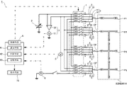
図1は、本発明に係る絶縁検査装置の一実施形態の概略構成図である。
本発明に係る第一実施形態の絶縁検査装置1は、電流供給手段2、第一電圧検出手段3、電流検出手段4、第二電圧検出手段5、制御手段6、切替手段7、電流供給端子8、電圧検出端子9、表示手段10を備えてなる。
図1で示される一実施形態では、本発明の絶縁検査装置1と、検査対象となる回路基板CBと、絶縁検査装置1と回路基板CBとを電気的に接続するコタンクトプローブCPが示されている。
この第一実施形態の絶縁検査装置1は、検査対象である配線パターンPに接続される電流供給端子と電圧測定端子の間の電圧差を用いることにより、スパークを検出する。これは、配線パターンPに接続される電流供給端子と電圧測定端子が、スパークが発生しない限りにおいて、等電位であることを用いている。
The best mode for carrying out the present invention will be described.
The present invention relates to an insulation inspection apparatus and method for detecting a spark generated when an insulation inspection is performed on a plurality of wiring patterns formed on a circuit board.
FIG. 1 is a schematic configuration diagram of an embodiment of an insulation inspection apparatus according to the present invention.
The
In one embodiment shown in FIG. 1, an
The
図1に示される回路基板CBは、4つの配線パターンP1〜P4を有している。この回路基板CBが有する配線パターンは、設計される回路基板CBに応じてその数及び形状が適宜設定される。
尚、図1の回路基板CBでは、一の字状の配線パターンP1と、Tの字状の配線パターンP2と、十の字状の配線パターンP3とP4が示されている。
図1では、各配線パターンP1〜P4に電気的に接触する4本のコンタクトプローブCPが示されている。このコンタクトプローブCPは、絶縁検査装置1と回路基板CBを電気的に導通可能に接続する。また、このコンタクトプローブCPの配置位置や配置本数は、回路基板CBに形成される配線パターンに応じて適宜設定されることになる。
尚、図1の実施形態では、後述する上流側及び下流側電流供給端子と上流側及び下流側電圧検出端子とを1本のコンタクトプローブCPで、配線パターン上に設けられる所定検査位置に導通可能に接触させているが、電流供給端子と電圧検出端子の夫々を別々の2本のコンタクトプローブCPで所定検査位置に導通可能に接触させてもよい。
The circuit board CB shown in FIG. 1 has four wiring patterns P1 to P4. The number and shape of the wiring patterns of the circuit board CB are appropriately set according to the designed circuit board CB.
In the circuit board CB of FIG. 1, a single-shaped wiring pattern P1, a T-shaped wiring pattern P2, and a cross-shaped wiring pattern P3 and P4 are shown.
In FIG. 1, four contact probes CP that are in electrical contact with the wiring patterns P1 to P4 are shown. The contact probe CP connects the
In the embodiment of FIG. 1, the upstream and downstream current supply terminals and the upstream and downstream voltage detection terminals, which will be described later, can be electrically connected to a predetermined inspection position provided on the wiring pattern with a single contact probe CP. However, each of the current supply terminal and the voltage detection terminal may be brought into contact with a predetermined inspection position by two separate contact probes CP.
電流供給手段2は、検査対象となる配線パターンと他の配線パターンとの間(以下、検査対象間)に、絶縁検査を行うための所定の電圧を印加させる。
この電流供給手段2は、例えば、カレント・コントローラー(Current Controller)を用いることができるが特に限定されるものではなく、検査対象間に所定の電圧を印加させることができるものであれば全て用いることができる。カレント・コントローラーを用いる場合では、カレント・コントローラーである電流供給手段2により、所定の配線パターンに電流を供給して、検査対象間に所定の電圧を印加することになる。
この電流供給手段2が印加することになる電圧は、上記の説明の如き200〜250Vに設定される。
The current supply means 2 applies a predetermined voltage for performing an insulation test between a wiring pattern to be inspected and another wiring pattern (hereinafter, between inspection objects).
For example, a current controller can be used as the
The voltage to be applied by the current supply means 2 is set to 200 to 250 V as described above.
第一電圧検出手段3は、検査対象間の電圧を検出する。この第一電圧検査手段3は、例えば、電圧計を用いることができるが特に限定されるものではなく、検査対象間の電圧を検出することができるものであればよい。
この第一電圧検出手段3が検出する電圧値と、電流供給手段2により供給される電流値とを用いることによって、検査対象間の抵抗値を算出することができる。さらに、この抵抗値を用いることによって、検査対象間の絶縁性を検査することができる。
尚、この第一電圧検出手段3が検出する電圧値によって、電流供給手段2の動作の制御を行うように設定される。
The first voltage detection means 3 detects a voltage between inspection objects. For example, a voltmeter can be used as the first
By using the voltage value detected by the first voltage detection means 3 and the current value supplied by the current supply means 2, the resistance value between the inspection objects can be calculated. Further, by using this resistance value, it is possible to inspect the insulation between inspection objects.
The operation of the current supply means 2 is controlled according to the voltage value detected by the first voltage detection means 3.
電流検出手段4は、検査対象間の電流を検出する。この電流検出手段4は、例えば、電流計を用いることができるが特に限定されるものではなく、検査対象間に流れる電流値を検出することができればよい。
尚、電流供給手段2により供給される電流値を決定することもできるが、この電流検出手段4を用いることによっても、検査対象間の電流値を検出することもできる。
The current detection means 4 detects a current between inspection objects. For example, an ammeter can be used as the current detection unit 4, but the current detection unit 4 is not particularly limited as long as it can detect a current value flowing between inspection objects.
Although the current value supplied by the current supply means 2 can be determined, the current value between inspection objects can also be detected by using the current detection means 4.
電流供給端子8は、検査対象間の電流を供給するために、各配線パターンPとコンタクトプローブCPを介して接続される。
この電流供給端子8は、電流供給手段2の上流側(正極側)と配線パターンを接続する上流側電流供給端子81と、電流供給手段2の下流側(負極側)又は電流検出手段4と配線パターンPとを接続する下流側電流供給端子82を有している。
図1で示される如く、この電流供給端子8の上流側電流供給端子81及び下流側電流供給端子82は、夫々の配線パターンPに対して設けられている。
これらの上流側電流供給端子81と下流側電流供給端子82は、夫々に切替手段7のスイッチ素子SWを有しており、この切替手段7のスイッチ素子SWのON/OFF動作により、接続状態/未接続状態が設定されることになる。
この電流供給端子8は、静電気放電(electro-static discharge)保護用の抵抗が配置される。
The
The
As shown in FIG. 1, an upstream
Each of the upstream
The
電圧検出端子9は、検査対象間の電圧を検出するために、各配線パターンPとコンタクトプローブCPを介して接続される。
この電圧検出端子9は、第一電圧検出手段3の上流側(正極側)と配線パターンPを接続する上流側電圧検出端子91と、第一電圧検出手段3の下流側(負極側)と配線パターンPを接続する下流側電圧検出端子92を有してなる。
図1で示される如く、この電圧検出端子9の上流側電圧検出端子91及び下流側電圧検出端子92は、夫々の配線パターンPに対して設けられている。
これらの上流側電圧検出端子91と下流側電圧検出端子92は、電流供給端子8と同様、夫々に切替手段7のスイッチ素子SWを有しており、この切替手段7のスイッチ素子SWのON/OFF動作により、接続状態/未接続状態が設定されることになる。
The
The
As shown in FIG. 1, the upstream
Each of the upstream
電流供給端子8と電圧検出端子9は、図1で示される如く、配線パターンPに導通接触する一本のコンタクトプローブCPに対して、4つの端子が配置されることになるとともに、各端子のON/OFF制御を行う4つのスイッチ素子SWが備えられることになる。
尚、図1では、上流側電流供給端子81の動作を制御するスイッチ素子を符号SW1とし、上流側電圧検出端子91の動作を制御するスイッチ素子を符号SW2とし、下流側電流供給端子82の動作を制御するスイッチ素子を符号SW3とし、下流側電圧検出端子92の動作を制御するスイッチ素子を符号SW4として示している。
As shown in FIG. 1, the
In FIG. 1, the switch element that controls the operation of the upstream
切替手段7は、上記した各コンタクトプローブCPに導通接続される複数のスイッチ素子SWから構成されている。この切替手段7は、後述する制御手段6からの動作信号により。ON/OFFの動作が制御されることになる。 The switching means 7 is composed of a plurality of switch elements SW that are conductively connected to the contact probes CP described above. This switching means 7 is based on an operation signal from the control means 6 described later. The ON / OFF operation is controlled.
第二電圧検出手段5は、上流側電流供給端子81と上流側電圧検出端子91の電圧を検出する。具体的には、この第二電圧検出手段5が、上流側電流供給端子81と上流側電圧検出端子91の電圧の差を検出する。
この第二電圧検出手段5は、図1で示される如く、上流側電流供給端子81と上流側電圧検出端子91の電圧の差分を算出するコンパレータ52とこの差分を検出する電圧計51を有して構成される。
このコンパレータ52が、上流側電流供給端子81と上流側電圧検出端子91との電圧の差分を求め、電圧計51がこの差分を検出することになる。
詳細は後述するが、この第二電圧検出手段5が検出する電圧値によって、検査対象となる配線パターンPと他の配線パターン間とのスパークを検出する。
The second voltage detection means 5 detects the voltages of the upstream
As shown in FIG. 1, the second voltage detection means 5 includes a
The
Although details will be described later, a spark between the wiring pattern P to be inspected and another wiring pattern is detected based on the voltage value detected by the second voltage detecting means 5.
第一電圧検出手段3、電流検出手段4や第二電圧検出手段5が検出する電圧値や電流値は、後述する制御手段6へ、経過時間情報が付与されて(時系列的な情報として)送信される。 The voltage value and current value detected by the first voltage detection means 3, the current detection means 4 and the second voltage detection means 5 are given elapsed time information to the control means 6 described later (as time-series information). Sent.
制御手段6は、検査対象となる配線パターンPを選出したり、第一電圧検出手段3や第二電圧検出手段5からの電圧値を基にスパークを検出したり、切替手段7の動作の指示信号を送信する。
この制御手段6は、図1で示される如く、選出手段61、判定手段62、記憶手段63を備えている。
The control means 6 selects the wiring pattern P to be inspected, detects a spark based on the voltage values from the first voltage detection means 3 and the second voltage detection means 5, and instructs the switching means 7 to operate. Send a signal.
The control means 6 includes a selection means 61, a determination means 62, and a storage means 63 as shown in FIG.
記憶手段63は、回路基板CBの配線パターンPに関する情報、この配線パターンPの検査点に関する情報、検出される検出値の情報が記憶される。
この記憶手段63に絶縁検査に必要な情報が格納され、これらの情報を用いることによって、絶縁検査が行われることになるとともに、検出される各検出値が格納される。
The storage means 63 stores information related to the wiring pattern P of the circuit board CB, information related to inspection points of the wiring pattern P, and information of detected values to be detected.
Information necessary for the insulation inspection is stored in the storage means 63, and by using these pieces of information, the insulation inspection is performed and each detected value to be detected is stored.
選出手段61は、回路基板CBの複数の配線パターンPから検査対象となる配線パターンPを選出し、検査対象の配線パターンPを特定する。この選出手段61が検査対象の配線パターンPを特定することにより、順次、絶縁検査が行われる配線パターンが選出される。
この選出手段61が行う検査対象の配線パターンの選出方法は、予め記憶手段63に検査対象となる配線パターンの順番が設定され、この順番に従って検査対象の配線パターンが選出される方法を例示することができる。この選出方法は、上記の如き方法を採用することもできるが、検査対象となる配線パターンが順序良く選出される方法であれば特に限定されない。
この選出手段61が行う具体的な配線パターンの選出は、切替手段7を用いることにより実施される。例えば、切替手段7の各スイッチ素子SWのON/OFF制御を行うことにより、検査対象となる配線パターンを選出することができる。
第一実施形態の絶縁検査装置では、検査対象となる配線パターンが電流供給手段2と接続されるための上流側電流供給端子81と接続されるように、スイッチ素子SWがONされることになる。また同時に、上流側電圧検出手段91とこの配線パターンが接続されるようにスイッチ素子SWがONされる。
例えば、図1で示される実施形態では、配線パターンP1を検査対象とする場合、選出手段61が、配線パターンP1に接続する上流側電流供給端子81と上流側電圧検出端子91を選出し、これら端子81、91のスイッチ素子SW1とスイッチ素子SW2をONさせるように促す信号を送信する。この信号を切替手段7が受信することにより、スイッチ素子SW1とスイッチ素子SW2が動作することになる。
また、この場合、検査対象の配線パターン以外の配線パターン(残りの配線パターン)に対応するスイッチSW4がONされるように促す信号が送信される。
The selection means 61 selects the wiring pattern P to be inspected from the plurality of wiring patterns P on the circuit board CB, and specifies the wiring pattern P to be inspected. When the selection means 61 specifies the wiring pattern P to be inspected, the wiring patterns to be subjected to the insulation inspection are sequentially selected.
The selection method of the wiring pattern to be inspected performed by the selection unit 61 is exemplified by a method in which the order of wiring patterns to be inspected is set in the storage unit 63 in advance, and the wiring pattern to be inspected is selected according to this order. Can do. This selection method can adopt the method as described above, but is not particularly limited as long as the wiring patterns to be inspected are selected in order.
The selection of a specific wiring pattern performed by the selection unit 61 is performed by using the switching unit 7. For example, a wiring pattern to be inspected can be selected by performing ON / OFF control of each switch element SW of the switching means 7.
In the insulation inspection apparatus of the first embodiment, the switch element SW is turned on so that the wiring pattern to be inspected is connected to the upstream
For example, in the embodiment shown in FIG. 1, when the wiring pattern P1 is an inspection target, the selection means 61 selects the upstream
In this case, a signal is transmitted that prompts the switch SW4 corresponding to a wiring pattern other than the wiring pattern to be inspected (remaining wiring patterns) to be turned on.
上記の説明の如く、選出手段61によって、回路基板CBの複数の配線パターンPから検査対象となる配線パターンPが選択されることになる。
この第一実施形態で示される絶縁検査装置1の選出手段61が選出する配線パターンPは、回路基板CB上に形成された複数の配線パターンから1本の配線パターンPが選出される。つまり、選出手段61により選出された1本の配線パターンPと、残り全ての配線パターンPとの間で絶縁検査が実施される。
このように、配線パターンPが選出されることにより、絶縁検査を効率良く処理することができる。
As described above, the selection means 61 selects the wiring pattern P to be inspected from the plurality of wiring patterns P on the circuit board CB.
As the wiring pattern P selected by the selection means 61 of the
Thus, by selecting the wiring pattern P, the insulation inspection can be processed efficiently.
判定手段62は、第二電圧検出手段5からの電圧値を基に、スパークの発生を判定する。この判定手段62が行う判定は、予め設定される閾値に対して、その閾値よりも検出される電圧値が上回れば、スパークが発生していると判定するように設定することができる。また、第二電圧検出手段5による電圧値を良品の場合の電圧値と比較して、その差分によりスパークの発生を検出するように設定することもできる。
尚、この判定手段62は、電圧値の時間的変化量からスパークを検出するようにすることもできる。
スパークが検出されると、後述する表示手段10にその旨が連絡される。
The determination unit 62 determines the occurrence of spark based on the voltage value from the second voltage detection unit 5. The determination performed by the determination means 62 can be set to determine that a spark has occurred if a voltage value detected above the threshold value exceeds the threshold value. It is also possible to set so that the voltage value by the second voltage detection means 5 is compared with the voltage value in the case of a non-defective product, and the occurrence of spark is detected by the difference.
The determination means 62 can also detect a spark from the temporal change amount of the voltage value.
When a spark is detected, a message to that effect is sent to the display means 10 described later.
この制御手段6には、スパークの大きさを検出する算出手段(図示せず)を設けることができる。この算出手段は、判定手段62がスパークを検出した場合に、その電圧値や経過時間などからスパークのエネルギー量を計算する。この算出手段の結果により、スパークの大きさを認識することが可能となり、回路基板CBに対する破損の大きさの度合いを認識することができる。
特に、本発明によるスパーク検出方法では、検出される電圧がスパークのみに起因する電圧変化が検出されるとともにその際の電流も検出することができるので、正確なスパークの大きさ(=I×V)を求めることができる。
The control means 6 can be provided with calculation means (not shown) for detecting the size of the spark. When the determination unit 62 detects a spark, the calculation unit calculates the amount of spark energy from the voltage value, elapsed time, and the like. As a result of the calculation means, it is possible to recognize the magnitude of the spark, and to recognize the degree of the magnitude of damage to the circuit board CB.
In particular, in the spark detection method according to the present invention, since the detected voltage can be detected as a voltage change due to only the spark and the current at that time can also be detected, an accurate spark magnitude (= I × V ).
表示手段10は、絶縁検査の状態を表示する。この表示手段10は、スパークの発見が表示されることになる。
制御手段6の算出手段がスパークの大きさを算出するように設定している場合、この算出されるスパークの大きさもこの表示手段10において表示される。
以上が本発明に係る第一実施形態の絶縁検査装置1の構成の説明である。
The display means 10 displays the state of insulation inspection. This display means 10 displays the discovery of the spark.
When the calculation means of the control means 6 is set to calculate the spark size, the calculated spark size is also displayed on the display means 10.
The above is description of the structure of the insulation test |
この第一実施形態の絶縁検査装置1の動作を説明する。
まず、検査対象となる回路基板CBの配線パターンPの情報などが記憶手段63に格納される。
次に、回路基板CBが所定の検査位置に配置され、回路基板CB上に形成される配線パターンP上の検査点にコンタクトプローブが配置される。
Operation | movement of the insulation test |
First, information on the wiring pattern P of the circuit board CB to be inspected is stored in the storage unit 63.
Next, the circuit board CB is arranged at a predetermined inspection position, and a contact probe is arranged at an inspection point on the wiring pattern P formed on the circuit board CB.
回路基板CBが準備されると絶縁検査が開始される。
この場合、選出手段61が、検査対象となる配線パターンPを選出する。選出手段61が検査対象となる配線パターンを選出すると、この選出手段61は切替手段7へこの検査対象として選出された配線パターンPの上流側電流供給端子81と上流側電圧検出端子91が特定される。そして、この特定された上流側電流供給端子81と上流側電圧検出端子91を接続状態とするためのスイッチ素子SW1、SW2がONされるように、選出手段61から動作信号が切替手段7へ送信される。
When the circuit board CB is prepared, an insulation test is started.
In this case, the selection means 61 selects the wiring pattern P to be inspected. When the selection unit 61 selects a wiring pattern to be inspected, the selection unit 61 specifies the upstream
切替手段7は、選出手段61からのスイッチ素子のON/OFF動作に関する信号を受信すると、この信号に従ってスイッチ素子SWのON/OFF制御が行われる。
例えば、配線パターンP1が検査対象の配線パターンとなる場合、配線パターンP1に対応する上流側電流供給端子81と上流側電圧検出端子91に接続されるスイッチ素子SW1、SW2がONとなる。またこのとき同時に、この配線パターンP1以外の配線パターンP2乃至配線パターンP4に接触されるコンタクトプローブCPが、夫々下流側電流供給端子82と接続状態となるために、夫々の下流側電流供給端子82のスイッチ素子SW4がONとなるように制御する。
尚、この場合、検査対象以外の配線パターンPに対応する下流側電圧検出端子92は、スイッチ素子SW3により、ON/OFFいずれの場合でも構わない。
When the switching means 7 receives a signal relating to the ON / OFF operation of the switch element from the selection means 61, ON / OFF control of the switch element SW is performed according to this signal.
For example, when the wiring pattern P1 is a wiring pattern to be inspected, the switch elements SW1 and SW2 connected to the upstream
In this case, the downstream
図2は、本発明に係る絶縁検査装置の動作状態を示す一実施形態である。この図2で示される動作状態では、上記の説明の如く、配線パターンP1が検査対象として選出されている。このため、配線パターンP1は、スイッチ素子SW1とスイッチSW2がONされており、上流側電流供給端子81と上流側電圧検出端子91と接続されている。
このとき、検査対象以外の配線パターンP2乃至配線パターンP4は、スイッチ素子SW4がONされて、下流側電流供給端子82と接続されている。
図2で示される如く、検査対象の配線パターンP1の上流側電流供給端子81と上流側電圧検出端子91が第二電圧検出手段5に接続される。
FIG. 2 is an embodiment showing the operating state of the insulation inspection apparatus according to the present invention. In the operation state shown in FIG. 2, as described above, the wiring pattern P1 is selected as an inspection target. For this reason, the switch pattern SW1 and the switch SW2 are turned on in the wiring pattern P1, and the upstream
At this time, the wiring patterns P2 to P4 other than the inspection target are connected to the downstream
As shown in FIG. 2, the upstream
上記の如きスイッチ素子SWが、ON又はOFF制御されると、検査対象の配線パターンP1に電流が印加される。
このとき、第二電圧検出手段5は、電圧値の変化を検出するとともに制御手段6へ電圧値を、この電圧値に関する時間情報を付与して送信する。
When the switch element SW as described above is ON or OFF controlled, a current is applied to the wiring pattern P1 to be inspected.
At this time, the second voltage detection means 5 detects a change in the voltage value and transmits the voltage value to the control means 6 with time information relating to the voltage value.
制御手段6は、電圧値を受け取ると、判定手段62において、この電圧値が所定閾値と比較される。このとき、電圧値が閾値よりも大きいと、判定手段62はスパークが発生した判定をし、その旨が表示手段10へ送られて表示されることになる。
When the control unit 6 receives the voltage value, the determination unit 62 compares the voltage value with a predetermined threshold value. At this time, if the voltage value is larger than the threshold value, the determination unit 62 determines that a spark has occurred, and the fact is sent to the
図3は、本発明の絶縁検査装置が検出する電圧値の変化を示す一実施例である。この図3(a)では、検査対象間のスパークの状態を示す電圧変化を示しており、図3(b)では、本発明に係る絶縁検査装置のスパーク検出の状態を示す電圧変化を示している。 FIG. 3 is an example showing a change in voltage value detected by the insulation inspection apparatus of the present invention. FIG. 3 (a) shows a voltage change indicating a spark state between inspection objects, and FIG. 3 (b) shows a voltage change indicating a spark detection state of the insulation inspection apparatus according to the present invention. Yes.
本発明に係る絶縁検査装置1は、上記の如く、上流側電流供給端子81と上流側電圧検出端子91の間の電圧の差を検出し、その差分によりスパークを検出する。
この場合、第一電圧検出手段3は、電流供給手段2が電流を配線パターンP1に供給し始めてから(時刻t1)、検出される電圧値が上昇する(検査対象となる配線パターン間の電圧)。ここで、絶縁検査に必要な所定電圧値になると(時刻t3)、絶縁検査が実行されることになる。この図3では、電流供給中である時刻t2と、絶縁検査中である時刻t4にスパークが発生していることが示される。
第二電圧検出手段5は、上流側電圧供給端子81と上流側電流検出端子91の間の電圧を検出する。この場合、電流供給手段2により電流が供給されている間(時刻t1〜時刻t3)は、保護抵抗に依存する電圧値が検出され、配線パターン間に所定の電圧が印加されると(時刻t3以降)、電圧値は略ゼロとなる。
この図3で示される場合には、時刻t2と時刻t4においてスパークが発生している。本発明の第一実施形態の絶縁検査装置1では、この第二電圧検出手段5がスパークを検出するが、図3で示される如く、スパークが発生した場合、急激な電圧変化を検出する。例えば、検査対象の配線パターンにチャージが行われている時刻t1〜時刻t3の間に、スパークが発生した場合、保護抵抗に流れる電圧が急激に上昇する(時刻t2)。この急激な電圧の上昇を検出することにより、スパークを検出することができる。
また、検査対象の配線パターンへのチャージが終了した後の検査対象の配線パターンと他の配線パターンとの絶縁検査が行われる際に発生するスパーク(時刻t4でのスパーク)が発生した場合、第二電圧検出手段5は略ゼロであった電圧から急激に上昇する電圧を検出する。特に、この場合では、スパークが発生しない間は第二電圧検出手段5が検出する電圧は略ゼロであるので、電圧に変化が生じることによりスパーク検出が容易に行われることになる。
As described above, the
In this case, the first voltage detection means 3 starts to supply current to the wiring pattern P1 from the current supply means 2 (time t1), and the detected voltage value increases (voltage between wiring patterns to be inspected). . Here, when the predetermined voltage value necessary for the insulation test is reached (time t3), the insulation test is executed. FIG. 3 shows that a spark is generated at time t2 during current supply and at time t4 during insulation inspection.
The second voltage detection means 5 detects the voltage between the upstream
In the case shown in FIG. 3, sparks occur at time t2 and time t4. In the
In addition, when a spark (spark at time t4) occurs when an insulation inspection between the wiring pattern to be inspected and another wiring pattern after the charging of the wiring pattern to be inspected is completed, The two-voltage detection means 5 detects a voltage that rises rapidly from a voltage that was substantially zero. In particular, in this case, the voltage detected by the second voltage detecting means 5 is substantially zero while no spark is generated, so that the spark detection is easily performed by the change in the voltage.
図3(b)では、制御手段6の判定手段62がスパークを検出するための閾値を設定して示されている。例えば、図3(b)で示される二点鎖線α(設定α)は、時刻t1から時刻t3間に保護抵抗にかかる電圧値よりも大きい電圧値に設定されている。この設定αの場合、第二電圧検出手段5が検出する電圧値が、設定値αを超えた時点でスパーク発生と判定することになる。この場合、設定αのみを設定することで容易にスパーク検出を行うことができる。 In FIG. 3B, the determination means 62 of the control means 6 shows a threshold value for detecting a spark. For example, a two-dot chain line α (setting α) shown in FIG. 3B is set to a voltage value larger than the voltage value applied to the protective resistance between time t1 and time t3. In the case of this setting α, it is determined that a spark has occurred when the voltage value detected by the second voltage detecting means 5 exceeds the setting value α. In this case, spark detection can be easily performed by setting only the setting α.
また、図3(b)で示される一点鎖線β(設定β)は、時刻t1から時刻t3までと、時刻t3以降と相違する設定値が設定されている。この設定βの場合は、第二電圧検出手段5が検出するチャージの場合の保護抵抗にかかる電圧値を補正している。このため、設定αの場合よりも、経過時間や第一電圧検出手段3による電圧検出結果によって電圧閾値を変更するように設定することで、より精度良くスパークを検出することができるようになる。
これら設定αと設定βは、使用者により適宜設定され、その具体的な設定値は、保護抵抗の抵抗値などに影響されるため使用者により適宜設定される。
Further, in the alternate long and short dash line β (setting β) shown in FIG. 3B, set values that are different from the time t1 to the time t3 and after the time t3 are set. In the case of this setting β, the voltage value applied to the protective resistance in the case of the charge detected by the second voltage detecting means 5 is corrected. Therefore, it is possible to detect the spark with higher accuracy by setting the voltage threshold to be changed according to the elapsed time and the voltage detection result by the first voltage detection means 3 than in the case of the setting α.
These settings α and β are appropriately set by the user, and the specific set values are appropriately set by the user because they are influenced by the resistance value of the protective resistance.
制御手段6がスパーク発生と判定すると、スパークが発生したことを表示手段10で表示する。また、このとき、算出手段によりスパークの大きさを算出する。
この算出手段が算出するスパークの大きさは、スパークを検出するための閾値よりも大きい電圧値が存在する面積を算出することができる。例えば、図3(b)で示される時刻t2で発生したスパークの大きさを算出する場合、設定αの設定値よりも大きい場所の面積を求めることによりその大きさを算出することができる(図3で示される二点鎖線αと電圧値変移により囲まれる部分(斜線で示す部分))。
この算出手段が算出するスパークの大きさも、表示手段10に表示されることになる。
When the control means 6 determines that a spark has occurred, the display means 10 displays that a spark has occurred. At this time, the size of the spark is calculated by the calculation means.
As the magnitude of the spark calculated by the calculating means, it is possible to calculate an area where a voltage value larger than a threshold value for detecting the spark exists. For example, when calculating the size of the spark generated at time t2 shown in FIG. 3B, the size can be calculated by obtaining the area of a place larger than the set value of the setting α (FIG. 3). A portion surrounded by an alternate long and two short dashes line α and a voltage value transition (a portion indicated by oblique lines)).
The size of the spark calculated by the calculation means is also displayed on the display means 10.
上記の如く、スパークが発生した場合には、スパークが発生したことが通知されるとともにそのスパークの大きさを算出し、スパークと同時にその大きさも表示されることになる。このため、使用者は、電圧値を検出することにより、容易に絶縁検査中に発生するスパークを検出することができるとともに、そのスパークの大きさも知ることができる。
この絶縁検査装置1では、検査対象となる一本の配線パターンと残り全ての配線パターンの絶縁検査が行われ、この検査対象の一本の配線パターンの絶縁検査が終了すると、検査対象として次の配線パターンが一本選択され、残り全ての配線パターンとの絶縁検査が繰り返し行われる。このようにして被検査基板に設けられる配線パターン全てが検査対象の配線パターンとして絶縁検査が行われる。
尚、検査途中でスパークが発生した被検査基板は、不良品として取り扱われる。
以上が本発明に係る第一実施形態の絶縁検査装置1の説明である。
As described above, when a spark occurs, it is notified that the spark has occurred, and the size of the spark is calculated, and the size is also displayed simultaneously with the spark. Therefore, the user can easily detect the spark generated during the insulation test by detecting the voltage value, and can also know the magnitude of the spark.
In this
A substrate to be inspected in which a spark has occurred during the inspection is handled as a defective product.
The above is description of the insulation test |
次に、本発明に係る第二実施形態の絶縁検査装置100について説明する。
第二実施形態の絶縁検査装置100と第一実施形態の絶縁検査装置1との相違は、検査対象となる配線パターンが、配線パターン間に設定される電位の高位(プラス側(上流側))に接続されるか電位の低位(マイナス側(下流側))に接続されているかである。第一実施形態の絶縁検査装置1では、この検査対象となる配線パターンが電位の高位に接続されており、一方、第二実施形態の絶縁検査装置100では、検査対象の配線パターンが電位の低位に接続されている。
この第二実施形態の絶縁検査装置100は、第一実施形態の絶縁検査装置1と同様に、検査対象となる配線パターンに接続される電圧検出端子と電流供給端子との電圧を検出することによって、スパークを検出する。
Next, the insulation inspection apparatus 100 of 2nd embodiment which concerns on this invention is demonstrated.
The difference between the insulation inspection apparatus 100 of the second embodiment and the
The insulation inspection apparatus 100 according to the second embodiment, like the
図4は、本発明に係る第二実施形態の絶縁検査装置の概略構成を示している。
本発明に係る第二実施形態の絶縁検査装置100は、電流供給手段2、第一電圧検出手段3、電流検出手段4、第二電圧検出手段50、制御手段6、切替手段7、電流供給端子8、電圧検出端子9、表示手段10を備えてなる。
この図2で示される第二実施形態では、第一実施形態と同様に、本発明の絶縁検査装置100と、検査対象となる回路基板CBと、絶縁検査装置1と回路基板CBとを電気的に接続するコタンクトプローブCPが示されている。
この第二実施形態の絶縁検査装置100は、上記の如く、検査対象である配線パターンPに接続される電流供給端子と電圧測定端子の間の電圧差を用いることにより、スパークを検出する。これは、配線パターンPに接続される電流供給端子と電圧測定端子が、スパークが発生しない限りにおいて、等電位であることを用いている。
第一実施形態では、一本の配線パターンを電位の高位側に接続し、残り全ての配線パターンを電位の低位側に接続して絶縁検査を行う。これに対して、第二実施形態では、一本の配線パターンを電位の低位側に接続し、残り全ての配線パターンを電位の高位側に接続して絶縁検査を行う。このため、第一実施形態と第二実施形態では、検査対象に対する接続が相違している。このため、第一実施形態の構成と第二実施形態の構成が同一の場合には、詳細な説明を省略する。
FIG. 4 shows a schematic configuration of an insulation inspection apparatus according to the second embodiment of the present invention.
The insulation inspection apparatus 100 according to the second embodiment of the present invention includes a
In the second embodiment shown in FIG. 2, as in the first embodiment, the insulation inspection apparatus 100 of the present invention, the circuit board CB to be inspected, the
As described above, the insulation inspection apparatus 100 according to the second embodiment detects a spark by using the voltage difference between the current supply terminal connected to the wiring pattern P to be inspected and the voltage measurement terminal. This uses the fact that the current supply terminal and the voltage measurement terminal connected to the wiring pattern P are equipotential as long as no spark occurs.
In the first embodiment, one wiring pattern is connected to the higher potential side, and all the remaining wiring patterns are connected to the lower potential side to perform an insulation test. On the other hand, in the second embodiment, one wiring pattern is connected to the lower potential side, and all the remaining wiring patterns are connected to the higher potential side to perform the insulation test. For this reason, the connection with respect to a test object is different in the first embodiment and the second embodiment. For this reason, when the structure of 1st embodiment and the structure of 2nd embodiment are the same, detailed description is abbreviate | omitted.
図4に示される回路基板CBは、図1で示される回路基板CBと同様に、4つの配線パターンP1〜P4を有している。図4では、さらに、各配線パターンP1〜P4に電気的に接触する4本のコンタクトプローブCPが示されている。このコンタクトプローブCPは、絶縁検査装置1と回路基板CBを電気的に導通可能に接続する。
The circuit board CB shown in FIG. 4 has four wiring patterns P1 to P4, like the circuit board CB shown in FIG. FIG. 4 further shows four contact probes CP that are in electrical contact with the wiring patterns P1 to P4. The contact probe CP connects the
電流供給手段2は、第一実施形態の場合と同様、検査対象となる配線パターンと他の配線パターンとの間(以下、検査対象間)に、絶縁検査を行うための所定の電圧を印加させる。
尚、この電流供給手段2は、検査対象の配線パターン以外の全ての配線パターンに電流を供給する。
As in the case of the first embodiment, the current supply means 2 applies a predetermined voltage for performing an insulation test between a wiring pattern to be inspected and another wiring pattern (hereinafter, between inspection objects). .
The current supply means 2 supplies current to all wiring patterns other than the wiring pattern to be inspected.
第一電圧検出手段3は、第一実施形態の場合と同様、検査対象間の電圧を検出する。
この第一電圧検出手段3が検出する電圧値と、電流供給手段2により供給される電流値とを用いることによって、検査対象間の抵抗値を算出することができる。さらに、この抵抗値を用いることによって、検査対象間の絶縁性を検査することができる。
電流検出手段4は、第一実施形態の場合と同様、検査対象間の電流を検出する。
The first voltage detection means 3 detects the voltage between the inspection objects as in the case of the first embodiment.
By using the voltage value detected by the first voltage detection means 3 and the current value supplied by the current supply means 2, the resistance value between the inspection objects can be calculated. Further, by using this resistance value, it is possible to inspect the insulation between inspection objects.
The current detection means 4 detects the current between the inspection objects as in the case of the first embodiment.
電流供給端子8は、第一実施形態の場合と同様、検査対象間の電流を供給するために、各配線パターンPとコンタクトプローブCPを介して接続される。
この電流供給端子8は、電流供給手段2の上流側(正極側)と配線パターンを接続する上流側電流供給端子81と、電流供給手段2の下流側(負極側)又は電流検出手段4と配線パターンPとを接続する下流側電流供給端子82を有している。
図3で示される如く、この電流供給端子8の上流側電流供給端子81及び下流側電流供給端子82は、夫々の配線パターンPに対して設けられている。
これらの上流側電流供給端子81と下流側電流供給端子82は、夫々に切替手段7のスイッチ素子SWを有しており、この切替手段7のスイッチ素子SWのON/OFF動作により、接続状態/未接続状態が設定されることになる。
この電流供給端子8は、静電気放電(electro-static discharge)保護用の抵抗が配置される。
As in the case of the first embodiment, the
The
As shown in FIG. 3, the upstream
Each of the upstream
The
電圧検出端子9は、第一実施形態の場合と同様、検査対象間の電圧を検出するために、各配線パターンPとコンタクトプローブCPを介して接続される。
この電圧検出端子9は、第一電圧検出手段3の上流側(正極側)と配線パターンPを接続する上流側電圧検出端子91と、第一電圧検出手段3の下流側(負極側)と配線パターンPを接続する下流側電圧検出端子92を有してなる。
図3で示される如く、この電圧検出端子9の上流側電圧検出端子91及び下流側電圧検出端子92は、夫々の配線パターンPに対して設けられている。
これらの上流側電圧検出端子91と下流側電圧検出端子92は、電流供給端子8と同様、夫々に切替手段7のスイッチ素子SWを有しており、この切替手段7のスイッチ素子SWのON/OFF動作により、接続状態/未接続状態が設定されることになる。
Similarly to the case of the first embodiment, the
The
As shown in FIG. 3, the upstream
Each of the upstream
電流供給端子8と電圧検出端子9は、第一実施形態の場合と同様、配線パターンPに導通接触する一本のコンタクトプローブCPに対して、4つの端子が配置されることになるとともに、各端子のON/OFF制御を行う4つのスイッチ素子SWが備えられることになる。
尚、図1では、上流側電流供給端子81の動作を制御するスイッチ素子を符号SW1とし、上流側電圧検出端子91の動作を制御するスイッチ素子を符号SW2とし、下流側電流供給端子82の動作を制御するスイッチ素子を符号SW3とし、下流側電圧検出端子92の動作を制御するスイッチ素子を符号SW4として示している。
As in the case of the first embodiment, the
In FIG. 1, the switch element that controls the operation of the upstream
切替手段7は、上記した各コンタクトプローブCPに導通接続される複数のスイッチ素子SWから構成されている。この切替手段7は、後述する制御手段6からの動作信号により。ON/OFFの動作が制御されることになる。 The switching means 7 is composed of a plurality of switch elements SW that are conductively connected to the contact probes CP described above. This switching means 7 is based on an operation signal from the control means 6 described later. The ON / OFF operation is controlled.
この第二実施形態の絶縁検査装置100は、第二切替手段71を有している。この第二切替手段71は、下流側電流供給端子82を上流側電流供給端子81と等電位となるように接続させたり、第一電圧検出手段3の第一電圧検出手段3の下流側と接続させたりする。この図4では、第一電圧検出手段3の下流側と接続されるとともに電流検出手段4と直列接続される。
この第二切替手段71は、上記の如く、検査対象の配線パターンに接続される下流側電流供給端子82を、電流供給手段2の上流側又は電流検出手段4の上流側に接続するが、電流供給手段2の上流側に接続される場合には、上流側電流供給端子81と等電位とすることができる。
つまり、第二実施形態の絶縁検査装置100では、全ての配線パターンを先ずチャージすることになる。
第二切替手段71が、下流側電流供給端子82を電流検出手段4の上流側に接続すると、検査対象の配線パターンの電位が降下することになる。
このため、第二切替手段71は、検査対象の配線パターンの電位の高低を制御することができる。
The insulation inspection apparatus 100 according to the second embodiment has second switching means 71. The second switching means 71 connects the downstream
As described above, the second switching unit 71 connects the downstream
That is, in the insulation inspection apparatus 100 of the second embodiment, all wiring patterns are charged first.
When the second switching means 71 connects the downstream
For this reason, the second switching means 71 can control the level of the potential of the wiring pattern to be inspected.
第二実施形態の絶縁検査装置100は、第二切替手段71により検査対象の配線パターンの電位を降下させることができるが、この降下を制御するために電圧制御手段2’を設けることが好ましい。
この電圧制御手段2’を設けることによって、第二切替手段71により検査対象の配線パターンの電位を降下させる場合に、その降下量を制御することができる。このように降下量を制御することによって、検査対象の配線パターンと他の配線パターン間で、検査対象の配線パターンの電位の降下時間を制御し、この降下時におけるスパークの検出を確実に行うことができるようになる。
In the insulation inspection apparatus 100 of the second embodiment, the potential of the wiring pattern to be inspected can be lowered by the second switching means 71, but it is preferable to provide the voltage control means 2 ′ in order to control this drop.
By providing the voltage control means 2 ′, when the potential of the wiring pattern to be inspected is lowered by the second switching means 71, the amount of the drop can be controlled. By controlling the amount of descent in this way, the potential drop time of the wiring pattern to be inspected is controlled between the wiring pattern to be inspected and other wiring patterns, and the spark is reliably detected during this descent. Will be able to.
第二電圧検出手段50は、下流側電流供給端子82と下流側電圧検出端子92の電圧を検出する。具体的には、この第二電圧検出手段50が、下流側電流供給端子82と下流側電圧検出端子92の電圧の差を検出する。
この第二電圧検出手段50は、図3で示される如く、下流側電流供給端子82と下流側電圧検出端子92の電圧の差分を算出するコンパレータ54とこの差分を検出する電圧計53を有して構成される。
このコンパレータ54が、下流側電流供給端子82と下流側電圧検出端子92との電圧の差分を求め、電圧計53がこの差分を検出することになる。
詳細は後述するが、この第二電圧検出手段50が検出する電圧値によって、検査対象となる配線パターンPと他の配線パターン間とのスパークを検出する。
The second voltage detection means 50 detects the voltages of the downstream
As shown in FIG. 3, the second voltage detection means 50 includes a comparator 54 that calculates a difference between the voltages of the downstream
The comparator 54 obtains the voltage difference between the downstream
Although details will be described later, a spark between the wiring pattern P to be inspected and another wiring pattern is detected based on the voltage value detected by the second
第一電圧検出手段3、電流検出手段4や第二電圧検出手段5が検出する電圧値や電流値は、後述する制御手段6へ、第一実施形態の場合と同様、経過時間情報が付与されて(時系列的な情報として)送信される。 The voltage value and current value detected by the first voltage detection means 3, the current detection means 4, and the second voltage detection means 5 are given elapsed time information to the control means 6 described later, as in the first embodiment. (As time-series information).
制御手段6は、検査対象となる配線パターンPを選出したり、第一電圧検出手段3や第二電圧検出手段5からの電圧値を基にスパークを検出したり、切替手段7の動作の指示信号を送信する。
この制御手段6は、第一実施形態の場合と同様、第一電圧検出手段3や第二電圧検出手段50からの電圧値を基にスパーク検出したり、切替手段7の動作の指示信号を送信したりする。
この制御手段6は、図1で示される如く、選出手段61、判定手段62、記憶手段63を備えている。
The control means 6 selects the wiring pattern P to be inspected, detects a spark based on the voltage values from the first voltage detection means 3 and the second voltage detection means 5, and instructs the switching means 7 to operate. Send a signal.
As in the case of the first embodiment, the control means 6 performs spark detection based on the voltage values from the first voltage detection means 3 and the second voltage detection means 50, and transmits an instruction signal for the operation of the switching means 7. To do.
The control means 6 includes a selection means 61, a determination means 62, and a storage means 63 as shown in FIG.
選出手段61は、回路基板CBの複数の配線パターンPから検査対象となる配線パターンPを選出し、検査対象の配線パターンPを特定する。この選出手段61が検査対象の配線パターンPを特定することにより、順次、絶縁検査が行われる配線パターンが選出される。
この選出手段61が行う検査対象の配線パターンの選出方法は、予め記憶手段63に検査対象となる配線パターンの順番が設定され、この順番に従って検査対象の配線パターンが選出される方法を例示することができる。この選出方法は、上記の如き方法を採用することもできるが、検査対象となる配線パターンが順序良く選出される方法であれば特に限定されない。
この選出手段61が行う具体的な配線パターンの選出は、切替手段7を用いることにより実施される。例えば、切替手段7の各スイッチ素子SWのON/OFF制御を行うことにより、検査対象となる配線パターンを選出することができる。
第二実施形態の絶縁検査装置100では、検査対象となる配線パターンに対応するスイッチ素子SW3がONされる。このとき、スイッチ素子SW4がONされても構わない。
また、検査対象に選出されなかった残りの配線パターンは、この配線パターンに対応するスイッチ素子SW1とスイッチ素子SW2がONされることになる。
The selection means 61 selects the wiring pattern P to be inspected from the plurality of wiring patterns P on the circuit board CB, and specifies the wiring pattern P to be inspected. When the selection means 61 specifies the wiring pattern P to be inspected, the wiring patterns to be subjected to the insulation inspection are sequentially selected.
The selection method of the wiring pattern to be inspected performed by the selection unit 61 is exemplified by a method in which the order of wiring patterns to be inspected is set in the storage unit 63 in advance, and the wiring pattern to be inspected is selected according to this order. Can do. This selection method can adopt the method as described above, but is not particularly limited as long as the wiring patterns to be inspected are selected in order.
The selection of a specific wiring pattern performed by the selection unit 61 is performed by using the switching unit 7. For example, a wiring pattern to be inspected can be selected by performing ON / OFF control of each switch element SW of the switching means 7.
In the insulation inspection apparatus 100 of the second embodiment, the switch element SW3 corresponding to the wiring pattern to be inspected is turned on. At this time, the switch element SW4 may be turned on.
For the remaining wiring patterns that are not selected for inspection, the switch elements SW1 and SW2 corresponding to the wiring patterns are turned on.
この制御手段6は、第二切替手段71の動作も制御し、上記の如く、検査対象の配線パターンの電位を制御することになる。 The control means 6 also controls the operation of the second switching means 71 and controls the potential of the wiring pattern to be inspected as described above.
例えば、図5又は図6で示される実施形態では、配線パターンP1を検査対象とする場合を示している。この場合、選出手段61が、配線パターンP1に接続する下流側電流供給端子82と下流側電圧検出端子92を選出し、これら端子82、92のスイッチ素子SW3とスイッチ素子SW4をONさせるように信号を送信する。
この信号を切替手段7が受信することにより、スイッチ素子SW3とスイッチ素子SW4が動作することになる。
また、同時に、検査対象となる配線パターン以外の配線パターン(残りの配線パターン)に対応するスイッチ素子SW1とスイッチ素子SW2がONされるよう促す信号を送信する。
For example, in the embodiment shown in FIG. 5 or FIG. 6, the case where the wiring pattern P1 is an inspection target is shown. In this case, the selection means 61 selects the downstream
When the switching unit 7 receives this signal, the switch element SW3 and the switch element SW4 operate.
At the same time, a signal that prompts the switch elements SW1 and SW2 corresponding to wiring patterns other than the wiring pattern to be inspected (remaining wiring patterns) to be turned on is transmitted.
上記の説明の如く、選出手段61によって、回路基板CBの複数の配線パターンPから検査対象となる配線パターンPが選択されることになる。
この第二実施形態で示される絶縁検査装置100の選出手段61が選出する配線パターンPは、回路基板CB上に形成された複数の配線パターンから1本の配線パターンPが選出される。つまり、選出手段61により選出された1本の配線パターンPと、残り全ての配線パターンPとの間で絶縁検査が実施される。
このように、配線パターンPが選出されることにより、絶縁検査を効率良く処理することができる。
As described above, the selection means 61 selects the wiring pattern P to be inspected from the plurality of wiring patterns P on the circuit board CB.
As the wiring pattern P selected by the selection means 61 of the insulation inspection apparatus 100 shown in the second embodiment, one wiring pattern P is selected from a plurality of wiring patterns formed on the circuit board CB. That is, an insulation inspection is performed between one wiring pattern P selected by the selection means 61 and all the remaining wiring patterns P.
Thus, by selecting the wiring pattern P, the insulation inspection can be processed efficiently.
判定手段62は、第二電圧検出手段5からの電圧値を基に、スパークの発生を判定する。この判定手段62が行う判定は、予め設定される閾値に対して、その閾値よりも検出される電圧値が上回れば、スパークが発生していると判定するように設定することができる。また、第二電圧検出手段5による電圧値を良品の場合の電圧値と比較して、その差分によりスパークの発生を検出するように設定することもできる。
尚、この判定手段62は、電圧値の時間的変化量からスパークを検出するようにすることもできる。
スパークが検出されると、後述する表示手段10にその旨が連絡される。
The determination unit 62 determines the occurrence of spark based on the voltage value from the second voltage detection unit 5. The determination performed by the determination means 62 can be set to determine that a spark has occurred if a voltage value detected above the threshold value exceeds the threshold value. It is also possible to set so that the voltage value by the second voltage detection means 5 is compared with the voltage value in the case of a non-defective product, and the occurrence of spark is detected by the difference.
The determination means 62 can also detect a spark from the temporal change amount of the voltage value.
When a spark is detected, a message to that effect is sent to the display means 10 described later.
この制御手段6には、スパークの大きさを検出する算出手段(図示せず)を設けることができる。この算出手段は、判定手段62がスパークを検出した場合に、その電圧値や経過時間などからスパークのエネルギー量を計算する。この算出手段の結果により、スパークの大きさを認識することが可能となり、回路基板CBに対する破損の大きさの度合いを認識することができる。 The control means 6 can be provided with calculation means (not shown) for detecting the size of the spark. When the determination unit 62 detects a spark, the calculation unit calculates the amount of spark energy from the voltage value, elapsed time, and the like. As a result of the calculation means, it is possible to recognize the magnitude of the spark, and to recognize the degree of the magnitude of damage to the circuit board CB.
表示手段10は、絶縁検査の状態を表示する。この表示手段10は、スパークの発見が表示されることになる。
制御手段6の算出手段がスパークの大きさを算出するように設定している場合、この算出されるスパークの大きさもこの表示手段10において表示される。
The display means 10 displays the state of insulation inspection. This display means 10 displays the discovery of the spark.
When the calculation means of the control means 6 is set to calculate the spark size, the calculated spark size is also displayed on the display means 10.
この第二実施形態の絶縁検査装置100の動作を説明する。
まず、検査対象となる回路基板CBの配線パターンPの情報などが記憶手段63に格納される。
次に、回路基板CBが所定の検査位置に配置され、回路基板CB上に形成される配線パターンP上の検査点にコンタクトプローブが配置される。
The operation of the insulation inspection apparatus 100 according to the second embodiment will be described.
First, information on the wiring pattern P of the circuit board CB to be inspected is stored in the storage unit 63.
Next, the circuit board CB is arranged at a predetermined inspection position, and a contact probe is arranged at an inspection point on the wiring pattern P formed on the circuit board CB.
回路基板CBが準備されると絶縁検査が開始される。
この場合、選出手段61が、検査対象となる配線パターンPを選出する。
選出手段61が検査対象となる配線パターンを選出すると、この選出手段61は切替手段7へこの検査対象として選出された配線パターンPの下流側電流供給端子82と下流側電圧検出端子92が特定される。そして、この特定された下流側電流供給端子82と下流側電圧検出端子92を接続状態とするためのスイッチ素子SW3、スイッチ素子SW4がONされるように、選出手段61から動作信号が切替手段7へ送信される。
When the circuit board CB is prepared, an insulation test is started.
In this case, the selection means 61 selects the wiring pattern P to be inspected.
When the selection unit 61 selects a wiring pattern to be inspected, the selection unit 61 specifies the downstream
切替手段7は、選出手段61からのスイッチ素子のON/OFF動作に関する信号を受信すると、この信号に従ってスイッチ素子SWのON/OFF制御が行われる。
例えば、配線パターンP1が検査対象の配線パターンとなる場合、配線パターンP1に対応する下流側電流供給端子82と下流側電圧検出端子92に接続されるスイッチ素子SW3、スイッチ素子SW4がONとなる。
またこのとき同時に、この配線パターンP1以外の配線パターンP2乃至配線パターンP4に接触されるコンタクトプローブCPが、夫々上流側電流供給端子81と上流側電圧検出端子91と接続状態となるために、夫々の上流側電流供給端子81のスイッチ素子SW1と上流側電圧検出端子91のスイッチ素子SW2とがONとなるように制御する。
この場合、第二切替手段71は、下流側電圧検出端子92を電流供給手段2の上流側に接続するように動作している(図5中のA側に接続される)。
尚、詳細は後述するが、上記の如き接続されることによって、全ての配線パターンに所定電圧を印加することになる。
When the switching means 7 receives a signal relating to the ON / OFF operation of the switch element from the selection means 61, ON / OFF control of the switch element SW is performed according to this signal.
For example, when the wiring pattern P1 is a wiring pattern to be inspected, the switch element SW3 and the switch element SW4 connected to the downstream
At the same time, the contact probes CP that are in contact with the wiring patterns P2 to P4 other than the wiring pattern P1 are connected to the upstream
In this case, the second switching means 71 operates so as to connect the downstream
Although details will be described later, a predetermined voltage is applied to all the wiring patterns by the connection as described above.
図5は、本発明に係る絶縁検査装置の動作状態を示す一実施形態である。この図5で示される動作状態では、上記の説明の如く、配線パターンP1が検査対象として選出されている。このため、配線パターンP1は、スイッチ素子SW3とスイッチSW4がONされており、下流側電流供給端子82と下流側電圧検出端子92と接続されている。
このとき、検査対象以外の配線パターンP2乃至配線パターンP4は、スイッチ素子SW1とスイッチ素子SW2がONされて、上流側電流供給端子81と上流側電圧検出端子91と接続されている。
ここで、図5で示される如く、検査対象の配線パターンP1の下流側電流供給端子82が電流供給手段2の上流側に接続され、下流側電圧検出端子92は第二電圧検出手段50の片側に接続される。
上記の如きスイッチ素子SWが、ON又はOFF制御されると、配線パターン全てにチャージが開始される。
FIG. 5 is an embodiment showing the operating state of the insulation inspection apparatus according to the present invention. In the operation state shown in FIG. 5, as described above, the wiring pattern P1 is selected as an inspection target. For this reason, in the wiring pattern P1, the switch element SW3 and the switch SW4 are turned on, and the downstream
At this time, the wiring patterns P2 to P4 other than the inspection target are connected to the upstream
Here, as shown in FIG. 5, the downstream
When the switch element SW as described above is ON or OFF controlled, charging is started for all the wiring patterns.
全ての配線パターンPの電位が所定電位に達すると、第二切替手段71はB側にスイッチが切り替えられる(図6参照)。このため、下流側電流供給端子92が第二電流検出手段4に接続されるとともに、検査対象の配線パターンP1の電位が低下する。この場合、電圧制御手段2’は、検査対象の配線パターンの電位の降下(降下量又は降下時間)の制御を行っており、この電圧降下時においても、検査対象の配線パターンと他の配線パターン間のスパークを検出することができる。
つまり、検査対象の配線パターンのみが電位の変化(低下)が生じることになり、検査対象の配線パターンP1と残りの配線パターンP2〜配線パターンP4との電位差が生じることになる。
このとき、検査対象間に絶縁不良が存在する場合にはスパークが発生する。このスパークによって、検査対象の配線パターンP1に電流が流入するため、下流側電流検出端子82と下流側電圧検出端子92には、電位差が生じることになる。
この結果、第二電圧検出手段50には、このスパークに起因する電圧が検出されることになる。
When the potentials of all the wiring patterns P reach a predetermined potential, the second switching means 71 is switched to the B side (see FIG. 6). For this reason, the downstream
That is, the potential change (decrease) occurs only in the wiring pattern to be inspected, and a potential difference occurs between the wiring pattern P1 to be inspected and the remaining wiring patterns P2 to P4.
At this time, if there is an insulation failure between inspection objects, a spark occurs. Due to this spark, a current flows into the wiring pattern P1 to be inspected, so that a potential difference is generated between the downstream
As a result, the second voltage detection means 50 detects the voltage resulting from this spark.
次に、第二切替手段71が、スイッチA側からB側に切り替えが行われて、十分な時間が経過した後、つまり、検査対象の配線パターンの電位が略ゼロに低下し、検査対象間に所定の電位差が生じた後に、検査対象間でスパークが発生した場合でも、検査対象の配線パターンP1にスパークに起因する電流が流入する。このため、下流側電流検出端子82と下流側電圧検出端子92には、電位差が生じることになる。
この結果、第二電圧検出手段50には、このスパークに起因する電圧が検出されることになる。
Next, after the second switching means 71 is switched from the switch A side to the B side and a sufficient time has elapsed, that is, the potential of the wiring pattern to be inspected decreases to substantially zero, Even if a spark occurs between inspection targets after a predetermined potential difference occurs, current caused by the spark flows into the wiring pattern P1 to be inspected. For this reason, a potential difference occurs between the downstream
As a result, the second voltage detection means 50 detects the voltage resulting from this spark.
制御手段6は、第二電圧検出手段50からの電圧値を受け取ると、判定手段62において、この電圧値が所定閾値と比較される。このとき、電圧値が閾値よりも大きいと、判定手段62はスパークが発生した判定し、その旨が表示手段10へ送られて表示されることになる。
When the control unit 6 receives the voltage value from the second
図7は、本発明の絶縁検査装置が検出する電圧値の変化を示す一実施例である。この図7(a)では、検査対象間のスパークの状態を示す電圧変化を示しており、図7(b)では、本発明に係る絶縁検査装置のスパーク検出の状態を示す電圧変化を示している。 FIG. 7 shows an example of a change in voltage value detected by the insulation inspection apparatus of the present invention. FIG. 7A shows a voltage change indicating a spark state between inspection objects, and FIG. 7B shows a voltage change indicating a spark detection state of the insulation inspection apparatus according to the present invention. Yes.
本発明に係る絶縁検査装置100は、上記の如く、検査対象の配線パターンの下流側電流供給端子82と下流側電圧検出端子92の間の電圧の差を検出し、その差分によりスパークを検出する。
この場合、第一電圧検出手段3は、図6で示される如く、電流供給手段2が電流を全ての配線パターンに供給し始めてから(時刻t5)、その電圧値が上昇する(検査対象となる全ての配線パターンが所定の電位まで上昇される)。
ここで、絶縁検査に必要な所定電圧値になると(時刻t6)、検査対象の配線パターンの電位を下げるため、第二切替手段71がスイッチをB側に接続する(時刻t7)。そうすると、図7(a)で示される如く、電圧値が低下して、略ゼロに至る(時刻t9)。
このとき、図7(a)で示される如く、時刻t8でスパークが発生した場合、下流側電圧供給端子82にスパークによる電流が流れる。そうすると、下流側電流供給端子82と下流側電圧検出端子92の間で、電位差が生じることになる。この結果、第二電圧検出手段50はこの電位差の電圧を検出することになる。このため、時刻t8でスパークが発生した場合には、第二電圧検出手段50がスパークによる電圧変化を検出することになる。
尚、この時刻t6と時刻t7の間の時間は、特にその長さが設定されておらず、使用者により適宜設定されるが、検査時間を短縮するためにもできるだけ短くすることが好ましい。また、電圧制御手段2’は、時刻t7と時刻t9の電位降下を制御することになる。
As described above, the insulation inspection apparatus 100 according to the present invention detects a voltage difference between the downstream
In this case, as shown in FIG. 6, the first voltage detection means 3 increases its voltage value (to be inspected) after the current supply means 2 starts supplying current to all the wiring patterns (time t5). All wiring patterns are raised to a predetermined potential).
Here, when the predetermined voltage value necessary for the insulation inspection is reached (time t6), the second switching means 71 connects the switch to the B side in order to lower the potential of the wiring pattern to be inspected (time t7). Then, as shown in FIG. 7A, the voltage value decreases and reaches substantially zero (time t9).
At this time, as shown in FIG. 7A, when a spark occurs at time t8, a current due to the spark flows through the downstream
The time between the time t6 and the time t7 is not particularly set, and is appropriately set by the user. However, it is preferable to shorten the time as much as possible in order to shorten the inspection time. The voltage control means 2 ′ controls the potential drop at time t7 and time t9.
検査対象の配線パターンの電圧が略ゼロになると、検査対象間の電位差が所定検査電圧に設定されることになり、絶縁検査が開始されることになる。尚、この場合、スパークが発生していない際において、第二電圧検出手段50は下流側電流供給端子82と下流側電圧検出端子92の電位の差は生じていない。このため、第二電圧検出手段50は、電位差ゼロであり、電圧ゼロを検出する。
このとき、検査対象間でスパークが発生した場合、この場合も上記と同様、検査対象の配線パターンに電流が流入することになり、第二電圧検出手段50が電圧の変化を検出する。
図7(b)では、時刻t10においてスパークが発生している。この場合も、スパークが発生することにより、検査対象の配線パターンに電流が流入し、この電流の流入によって、下流側電流供給端子82と下流側電圧検出端子92の間に電圧が生じることになる。そうすると、第二電圧検出手段50は、この電圧を検出し、制御手段6へ電圧値を送信する。
特に、このようなスパーク検出の場合、検査対象の配線パターンの電位を低下させて、所定の電圧を得て後の絶縁検査が行われる際に発生するスパーク(時刻t10の如きスパーク)が発生した場合、第二電圧検出手段5は略ゼロであった電圧から急激に上昇する電圧を検出する。このため、スパーク検出が容易に行われることになる。
When the voltage of the wiring pattern to be inspected becomes substantially zero, the potential difference between the inspection objects is set to a predetermined inspection voltage, and the insulation inspection is started. In this case, when no spark is generated, the second voltage detection means 50 does not cause a difference in potential between the downstream
At this time, when a spark occurs between inspection targets, in this case as well, a current flows into the wiring pattern to be inspected, and the second
In FIG. 7B, a spark occurs at time t10. Also in this case, the occurrence of a spark causes a current to flow into the wiring pattern to be inspected, and a voltage is generated between the downstream
In particular, in the case of such a spark detection, a spark (such as a time t10) generated when the potential of the wiring pattern to be inspected is reduced to obtain a predetermined voltage and a subsequent insulation inspection is performed. In this case, the second voltage detection means 5 detects a voltage that rapidly increases from a voltage that is substantially zero. For this reason, spark detection is easily performed.
図7(b)では、制御手段6の判定手段62がスパークを検出するための閾値を設定して示している。例えば、図7(b)で示される二点鎖線α(設定α)は、時刻t7から時刻t9間に保護抵抗にかかる電圧値よりも大きい電圧値に設定されている。この設定αの場合、第二電圧検出手段5が検出する電圧値が、設定値αを超えた時点でスパーク発生と判定することになる。この場合、設定αのみを設定することで容易にスパーク検出を行うことができる。 In FIG.7 (b), the determination means 62 of the control means 6 sets and shows the threshold value for detecting a spark. For example, a two-dot chain line α (setting α) shown in FIG. 7B is set to a voltage value larger than the voltage value applied to the protective resistance between time t7 and time t9. In the case of this setting α, it is determined that a spark has occurred when the voltage value detected by the second voltage detecting means 5 exceeds the setting value α. In this case, spark detection can be easily performed by setting only the setting α.
また、図7(b)で示される一点鎖線β(設定β)は、時刻t5から時刻t7前までと、時刻t7以降と相違する設定値が設定されている。この設定βの場合は、第二電圧検出手段5が検出するチャージの場合の保護抵抗にかかる電圧値を補正している。このため、設定αの場合よりも、より精度良くスパークを検出することができるようになる。
これら設定αと設定βは、使用者により適宜設定され、その具体的な設定値は、保護抵抗の抵抗値などに影響されるため使用者により適宜設定される。
この設定βの場合には、設定αに比して、経過時間や第一電圧検出手段3による電圧検出結果によって電圧閾値を変更するように設定することで、より精度良くスパークを検出することができるようになる。
Further, in the alternate long and short dash line β (set β) shown in FIG. 7B, set values that are different from time t5 to time t7 and after time t7 are set. In the case of this setting β, the voltage value applied to the protective resistance in the case of the charge detected by the second voltage detecting means 5 is corrected. For this reason, it becomes possible to detect the spark with higher accuracy than in the case of the setting α.
These settings α and β are appropriately set by the user, and the specific set values are appropriately set by the user because they are influenced by the resistance value of the protective resistance.
In the case of this setting β, it is possible to detect the spark with higher accuracy by setting the voltage threshold to be changed according to the elapsed time and the voltage detection result by the first voltage detection means 3 compared to the setting α. become able to.
制御手段6がスパーク発生と判定すると、スパークが発生したことを表示手段10で表示する。また、このとき、算出手段によりスパークの大きさを算出する。
この算出手段が算出するスパークの大きさは、スパークを検出するための閾値よりも大きい電圧値が存在する面積を算出することができる。例えば、図7で示される時刻t8で発生したスパークの大きさを算出する場合、設定αの設定値よりも大きい場所の面積を求めることによりその大きさを算出することができる(図7(b)で示される二点鎖線αと電圧値変移により囲まれる部分(斜線で示す部分))。
この算出手段が算出するスパークの大きさも、表示手段10に表示されることになる。
When the control means 6 determines that a spark has occurred, the display means 10 displays that a spark has occurred. At this time, the size of the spark is calculated by the calculation means.
As the magnitude of the spark calculated by the calculating means, it is possible to calculate an area where a voltage value larger than a threshold value for detecting the spark exists. For example, when calculating the size of the spark generated at time t8 shown in FIG. 7, the size can be calculated by obtaining the area of a place larger than the set value of the setting α (FIG. 7B). ) And a portion surrounded by a two-dot chain line α and a voltage value transition (a portion indicated by oblique lines)).
The size of the spark calculated by the calculation means is also displayed on the display means 10.
上記の如く、スパークが発生した場合には、スパークが発生したことが通知されるとともにそのスパークの大きさを算出し、スパークと同時にその大きさも表示されることになる。このため、使用者は、電圧値を検出することにより、容易に絶縁検査中に発生するスパークを検出することができるとともに、そのスパークの大きさも知ることができる。
この絶縁検査装置100では、検査対象となる一本の配線パターンと残り全ての配線パターンの絶縁検査が行われ、この検査対象の一本の配線パターンの絶縁検査が終了すると、検査対象として次の配線パターンが一本選択され、残り全ての配線パターンとの絶縁検査が繰り返し行われる。このようにして被検査基板に設けられる配線パターン全てが検査対象の配線パターンとして絶縁検査が行われる。
尚、検査途中でスパークが発生した被検査基板は、不良品として取り扱われる。
以上が本発明に係る第二実施形態の絶縁検査装置100の説明である。
As described above, when a spark occurs, it is notified that the spark has occurred, and the size of the spark is calculated, and the size is also displayed simultaneously with the spark. Therefore, the user can easily detect the spark generated during the insulation test by detecting the voltage value, and can also know the magnitude of the spark.
In this insulation inspection apparatus 100, the insulation inspection of one wiring pattern to be inspected and all the remaining wiring patterns is performed, and when the insulation inspection of one wiring pattern to be inspected is completed, the next inspection target is One wiring pattern is selected, and the insulation inspection with all the remaining wiring patterns is repeated. In this way, all the wiring patterns provided on the substrate to be inspected are subjected to insulation inspection as wiring patterns to be inspected.
A substrate to be inspected in which a spark has occurred during the inspection is handled as a defective product.
The above is the description of the insulation inspection apparatus 100 according to the second embodiment of the present invention.
図8は、本発明に係る第三実施形態の絶縁検査装置101の概略構成を示している。この第三実施形態の絶縁検査装置101は、基本的な構成は第二実施形態の絶縁検査装置100と同様に形成されているが、第二実施形態の絶縁検査装置100が有する第二切替手段71を有していない。
第二実施形態の絶縁検査装置100では、検査対象の配線パターンの電圧降下をこの第二切替手段71を用いて行っていたが、第三実施形態の絶縁検査装置101では、この検査対象の配線パターンの電位の制御を、この電圧制御手段2’を用いて行っている。
より具体的には、第三実施形態の絶縁検査装置101では、全ての配線パターンに所定電位を与える場合に、電圧制御手段2’と電流供給手段2が同電位を得るように設定される。次に、検査対象の配線パターンの電位を降下させる場合に、電圧制御手段2’が電流供給手段2の電位よりも低い電位を有するように制御させることによって、検査対象の配線パターンの電位を降下させる。
第三実施形態の絶縁検査装置101は、検査対象の配線パターンの電位を降下させる方法が、第二実施形態の絶縁検査装置100の第二切替手段71を用いる場合と異なる以外は、その検査方法は同様であるので、説明を省略する。
尚、この第三実施形態の絶縁検査装置101の電圧制御手段2’が接続される位置は、図8で示される位置に限定されず、検査対象となる配線パターンの下流側電流検出端子82と下流側電圧検出端子92にかかる電位を、制御することができる位置であれば特に限定されない。
FIG. 8 shows a schematic configuration of an insulation inspection apparatus 101 according to the third embodiment of the present invention. The insulation inspection apparatus 101 according to the third embodiment is basically formed in the same manner as the insulation inspection apparatus 100 according to the second embodiment. However, the second switching unit included in the insulation inspection apparatus 100 according to the second embodiment. 71 is not provided.
In the insulation inspection apparatus 100 according to the second embodiment, the voltage drop of the wiring pattern to be inspected is performed using the second switching unit 71. However, in the insulation inspection apparatus 101 according to the third embodiment, the wiring to be inspected is inspected. The pattern potential is controlled by using this voltage control means 2 '.
More specifically, in the insulation inspection apparatus 101 of the third embodiment, the voltage control means 2 ′ and the current supply means 2 are set to obtain the same potential when a predetermined potential is applied to all the wiring patterns. Next, when the potential of the wiring pattern to be inspected is lowered, the voltage control means 2 'is controlled so as to have a potential lower than the potential of the current supply means 2, thereby lowering the potential of the wiring pattern to be inspected. Let
The insulation inspection apparatus 101 according to the third embodiment is the same as the inspection method except that the method of lowering the potential of the wiring pattern to be inspected is different from the case of using the second switching means 71 of the insulation inspection apparatus 100 according to the second embodiment Are the same and will not be described.
Note that the position to which the voltage control means 2 ′ of the insulation inspection apparatus 101 of the third embodiment is connected is not limited to the position shown in FIG. 8, and the downstream
第一実施形態の絶縁検査装置1、第二実施形態の絶縁検査装置100と第三実施形態の絶縁検査装置101は、検査対象となる配線パターンに接続される上流側又は下流側に設定される電流供給端子と電圧検出端子と端子間の電圧を検出することにより、スパークを検出している。
このため、三つの絶縁検査装置ともに、スパークに起因する僅かな電圧の変化を検出することが可能となり、より精度の高い検査を行うことができる。
また、これら第一乃至第三実施形態の絶縁検査装置の概略構成を示す図面では、電圧検出端子と電流供給端子間の電圧を検出する場合に、静電気放電(ESD)保護用の抵抗とスイッチ素子SWを含む電圧を検出するように構成されているが、スイッチ素子SWの抵抗が含まれないようにすることによって、更に電圧検出の精度を向上させることもできる。この場合には、例えば、上流側電圧検出端子、上流側電流供給端子、下流側電圧検出端子と下流側電流供給端子を夫々2つ設けることによってスイッチ素子SWの抵抗分を消去するようにすることができる。
The
For this reason, it is possible to detect a slight voltage change caused by the spark in all three insulation inspection devices, and a more accurate inspection can be performed.
In the drawings showing the schematic configuration of the insulation inspection apparatus according to the first to third embodiments, when detecting a voltage between the voltage detection terminal and the current supply terminal, a resistance and a switch element for electrostatic discharge (ESD) protection Although configured to detect a voltage including SW, the accuracy of voltage detection can be further improved by not including the resistance of the switch element SW. In this case, for example, by providing two upstream voltage detection terminals, upstream current supply terminals, two downstream voltage detection terminals, and two downstream current supply terminals, the resistance component of the switch element SW is eliminated. Can do.
また、本発明に係るスパーク検出装置は、上記の如き電流供給端子と電圧検出端子間の電位を検出することによって、スパークを検出するものであるが、この電流供給端子と電圧検出端子やスイッチ素子は、図9(a)で示されるスイッチ回路構成に限定されない。例えば、図9(b)で示されるスイッチ回路構成では、図9(a)のスイッチ回路構成を基に、上流側電流供給端子81及び下流側電流供給端子82と上流側電圧検出端子91及び下流側電圧検出端子92の夫々に静電気放電保護用の抵抗Rが設けられている。
また、図9(c)にスイッチ回路構成では、電流供給端子8と電圧検出端子9が夫々一つの抵抗Rに接続され、且つ、上流側と下流側が並列に接続されることにより構成されている。
図9で示される何れのスイッチ回路構成も、使用者により適宜変更することが可能であり、本明細書中で説明した図9(a)の回路構成に限定されるものではない。
The spark detection device according to the present invention detects a spark by detecting the potential between the current supply terminal and the voltage detection terminal as described above. The current supply terminal, the voltage detection terminal, and the switch element Is not limited to the switch circuit configuration shown in FIG. For example, in the switch circuit configuration shown in FIG. 9B, based on the switch circuit configuration in FIG. 9A, the upstream
Further, in the switch circuit configuration shown in FIG. 9C, the
Any switch circuit configuration shown in FIG. 9 can be appropriately changed by the user, and is not limited to the circuit configuration shown in FIG. 9A described in this specification.
1・・・・・第一実施形態の絶縁検査装置
100・・・第二実施形態の絶縁検査装置
101・・・第三実施形態の絶縁検査装置
2・・・・・電流供給手段
3・・・・・第一電圧検出手段
4・・・・・電流検出手段
5・・・・・第二電圧検出手段
50・・・・第二電圧検出手段
6・・・・・制御手段
7・・・・・切替手段
71・・・・第二切替手段
81・・・・上流側電流供給端子
82・・・・下流側電流供給端子
91・・・・上流側電圧検出端子
92・・・・下流側電圧検出端子
P・・・・・配線パターン
DESCRIPTION OF
Claims (6)
前記複数の配線パターン毎に対応する、上流側に設定される該配線パターンに電流を供給する上流側電流供給端子と、
前記複数の配線パターン毎に対応する、下流側に設定される該配線パターンに導通接続される下流側電流供給端子と、
前記上流側電流供給端子と前記下流側電流供給端子とを介して、該配線パターン間に電圧を供給する電流供給手段と、
前記上流側電流供給端子と前記上流側に設定される配線パターンとの間に直列配置される抵抗体と、
前記複数の配線パターン毎に対応する、前記上流側に設定される配線パターンに導通接続される上流側電圧検出端子と、
前記複数の配線パターン毎に対応する、前記下流側に設定される配線パターンに導通接続される下流側電圧検出端子と、
前記上流側電圧検出端子と前記下流側電圧検出端子との間の電圧を検出する第一電圧検出手段と、
前記検査対象となる配線パターンに対応する上流側電流供給端子と上流側電圧検出端子との間の電圧を検出する第二電圧検出手段と、
前記第二電圧検出手段により検出される電圧値が予め設定される設定値を超えた場合に、前記検査対象の配線パターンと他の配線パターンとの間でスパーク発生と判定する判定手段とを備えることを特徴とする絶縁検査装置。 In the circuit board in which a plurality of wiring patterns are formed, from the plurality of wiring patterns, between the wiring pattern set on the downstream side and the wiring pattern set on the upstream side is selected as between wiring patterns to be inspected , An insulation inspection apparatus for performing an insulation inspection between the wiring patterns,
An upstream current supply terminal for supplying current to the wiring pattern set on the upstream side, corresponding to each of the plurality of wiring patterns;
A downstream-side current supply terminal that is conductively connected to the wiring pattern set on the downstream side, corresponding to each of the plurality of wiring patterns;
Through the upstream current supply terminal and the downstream current supply terminal, a current supply means for supplying a voltage between the wiring patterns,
A resistor which is arranged in series between the wiring pattern set in the upstream and the upstream current supply terminal,
An upstream voltage detection terminal that is conductively connected to the wiring pattern set on the upstream side, corresponding to each of the plurality of wiring patterns,
A downstream voltage detection terminal that is conductively connected to the wiring pattern set on the downstream side, corresponding to each of the plurality of wiring patterns;
A first voltage detecting means for detecting a voltage between the upstream-side voltage detecting terminal and the downstream voltage detecting terminal,
Second voltage detection means for detecting a voltage between the upstream current supply terminal and the upstream voltage detection terminal corresponding to the wiring pattern to be inspected;
And a determination unit that determines that a spark is generated between the wiring pattern to be inspected and another wiring pattern when a voltage value detected by the second voltage detection unit exceeds a preset value. insulation test apparatus characterized by.
前記上流側電圧検出端子及び前記上流側電流供給端子を、前記検査対象の配線パターンと導通状態とし、また、
前記下流側電圧検出端子及び前記下流側電流供給端子を、前記検査対象の配線パターン以外の全ての配線パターンと導通状態とすることを特徴とする請求項1記載の絶縁検査装置。 The insulation inspection apparatus further includes a switching unit, and the switching unit includes:
The upstream voltage detection terminal and the upstream current supply terminal are connected to the wiring pattern to be inspected , and
The downstream voltage detecting terminal and the downstream current supply terminals, insulation inspection apparatus according to claim 1, characterized in that a conductive state and all the wiring patterns other than the wiring pattern of said object.
前記複数の配線パターン毎に対応する、下流側に設定される該配線パターンに電流を供給する下流側電流供給端子と、
前記複数の配線パターン毎に対応する、上流側に設定される該配線パターンに導通接続される上流側電流供給端子と、
前記上流側電流供給端子と前記下流側電流供給端子を介して、該配線パターン間に電圧を供給する電流供給手段と、
前記下流側電流供給端子と前記下流側に設定される配線パターンとの間に直列配置される抵抗体と、
前記複数の配線パターン毎に対応する、前記下流側に設定される配線パターンに導通接続される下流側電圧検出端子と、
前記複数の配線パターン毎に対応する、前記上流側に設定される配線パターンに導通接続される上流側電圧検出端子と、
前記上流側電圧検出端子と前記下流側電圧検出端子との間の電圧を検出する第一電圧検出手段と、
前記検査対象となる配線パターンに対応する下流側電流供給端子と下流側電圧検出端子との間の電圧を検出する第二電圧検出手段と、
前記第二電圧検出手段により検出される電圧値が予め設定される設定値を超えた場合に、前記検査対象の配線パターンと他の配線パターンとの間でスパーク発生と判定する判定手段とを備えることを特徴とする絶縁検査装置。 In the circuit board in which a plurality of wiring patterns are formed, from the plurality of wiring patterns, between the wiring pattern set on the downstream side and the wiring pattern set on the upstream side is selected as between wiring patterns to be inspected An insulation inspection apparatus for performing an insulation inspection of the wiring pattern,
A downstream current supply terminal for supplying a current to the wiring pattern set on the downstream side, corresponding to each of the plurality of wiring patterns;
An upstream-side current supply terminal that is electrically connected to the wiring pattern set on the upstream side, corresponding to each of the plurality of wiring patterns;
Current supply means for supplying a voltage between the wiring patterns via the upstream current supply terminal and the downstream current supply terminal;
A resistor which is arranged in series between the wiring pattern set in said downstream side to the downstream current supply terminal,
A downstream voltage detection terminal that is conductively connected to the wiring pattern set on the downstream side, corresponding to each of the plurality of wiring patterns;
An upstream voltage detection terminal that is conductively connected to the wiring pattern set on the upstream side, corresponding to each of the plurality of wiring patterns,
A first voltage detecting means for detecting a voltage between the upstream-side voltage detecting terminal and the downstream voltage detecting terminal,
Second voltage detection means for detecting a voltage between a downstream current supply terminal and a downstream voltage detection terminal corresponding to the wiring pattern to be inspected;
And a determination unit that determines that a spark is generated between the wiring pattern to be inspected and another wiring pattern when a voltage value detected by the second voltage detection unit exceeds a preset value. insulation test apparatus characterized by.
前記下流側電流供給端子及び前記下流側電圧検出端子を、前記検査対象の配線パターンと導通状態とし、また、
前記上流側電流供給端子及び前記上流側電圧検出端子を、前記検査対象の配線パターン以外の全ての配線パターンと導通状態とすることを特徴とする請求項3記載の絶縁検査装置。 The insulation inspection apparatus further includes a switching unit, and the switching unit includes:
The downstream current supply terminal and the downstream voltage detection terminal are connected to the wiring pattern to be inspected , and
4. The insulation inspection apparatus according to claim 3, wherein the upstream current supply terminal and the upstream voltage detection terminal are brought into conduction with all wiring patterns other than the wiring pattern to be inspected.
回路基板上の複数の配線パターンから検査対象となる上流側及び下流側の配線パターンを選択する工程と、
前記複数の配線パターン毎に対応する、上流側に設定される該配線パターンに上流側電流供給端子を導通接続する工程と、
前記複数の配線パターン毎に対応する、下流側に設定される該配線パターンに下流側電流供給端子を導通接続する工程と、
前記上流側電流供給端子と前記上流側に設定される配線パターンとの間に抵抗体を直列に配置する工程と、
前記上流側電流供給端子と前記下流側電流供給端子とを介して、該配線パターン間に電圧を供給する工程と、
前記複数の配線パターン毎に対応する、前記上流側に設定される配線パターンに上流側電圧検出端子を導通接続する工程と、
前記複数の配線パターン毎に対応する、前記下流側に設定される配線パターンに下流側電圧検出端子を導通接続する工程と、
第一電圧検出手段によって、前記上流側電圧検出端子と前記下流側電圧検出端子との間の電圧を検出する工程と、
第二電圧検出手段によって、前記検査対象となる配線パターンに対応する上流側電流供給端子と上流側電圧検出端子との間の電圧を検出する工程と、
前記第二電圧検出手段により検出される電圧値が予め設定される設定値を超えた場合に、前記検査対象の配線パターンと他の配線パターンとの間でスパーク発生と判定する工程とを含むことを特徴とする絶縁検査方法。 In the circuit board in which a plurality of wiring patterns are formed, from the plurality of wiring patterns, between the wiring pattern set on the downstream side and the wiring pattern set on the upstream side is selected as between wiring patterns to be inspected An insulation inspection method for performing an insulation inspection between the wiring patterns,
Selecting an upstream and downstream wiring pattern to be inspected from a plurality of wiring patterns on the circuit board;
A step of electrically connecting an upstream current supply terminal to the wiring pattern set on the upstream side corresponding to each of the plurality of wiring patterns;
A step of conductively connecting a downstream current supply terminal to the wiring pattern set on the downstream side corresponding to each of the plurality of wiring patterns;
Placing a resistor in series between the upstream current supply terminal and the wiring pattern set on the upstream side;
Supplying a voltage between the wiring patterns via the upstream current supply terminal and the downstream current supply terminal;
A step of electrically connecting an upstream voltage detection terminal to the wiring pattern set on the upstream side corresponding to each of the plurality of wiring patterns;
A step of electrically connecting a downstream voltage detection terminal to the wiring pattern set on the downstream side corresponding to each of the plurality of wiring patterns;
A step of detecting a voltage between the upstream voltage detection terminal and the downstream voltage detection terminal by a first voltage detection means;
A step of detecting a voltage between the upstream current supply terminal and the upstream voltage detection terminal corresponding to the wiring pattern to be inspected by the second voltage detection means;
And determining that a spark has occurred between the wiring pattern to be inspected and another wiring pattern when the voltage value detected by the second voltage detecting means exceeds a preset value. Insulation inspection method characterized by.
回路基板上の複数の配線パターンから検査対象となる上流側及び下流側の配線パターンを選択する工程と、
前記複数の配線パターン毎に対応する、下流側に設定される該配線パターンに下流側電流供給端子を導通接続する工程と、
前記複数の配線パターン毎に対応する、上流側に設定される該配線パターンに上流側電流供給端子を導通接続する工程と、
前記下流側電流供給端子と前記下流側に設定される配線パターンとの間に抵抗体を直列配置する工程と、
前記上流側電流供給端子と前記下流側電流供給端子とを介して、該配線パターン間に電圧を供給する工程と、
前記複数の配線パターン毎に対応する、前記下流側に設定される配線パターンに下流側電圧検出端子を導通接続する工程と、
前記複数の配線パターン毎に対応する、前記上流側に設定される配線パターンに上流側電圧検出端子を導通接続する工程と、
第一電圧検出手段によって、前記上流側電圧検出端子と前記下流側電圧検出端子との間の電圧を検出する工程と、
第二電圧検出手段によって、前記検査対象となる配線パターンに対応する下流側電流供給端子と下流側電圧検出端子との間の電圧を検出する工程と、
前記第二電圧検出手段により検出される電圧値が予め設定される設定値を超えた場合に、前記検査対象の配線パターンと他の配線パターンとの間でスパーク発生と判定する工程とを含むことを特徴とする絶縁検査方法。 In the circuit board in which a plurality of wiring patterns are formed, from the plurality of wiring patterns, between the wiring pattern set on the downstream side and the wiring pattern set on the upstream side is selected as between wiring patterns to be inspected An insulation inspection method for performing an insulation inspection between the wiring patterns,
Selecting an upstream and downstream wiring pattern to be inspected from a plurality of wiring patterns on the circuit board;
A step of conductively connecting a downstream current supply terminal to the wiring pattern set on the downstream side corresponding to each of the plurality of wiring patterns;
A step of electrically connecting an upstream current supply terminal to the wiring pattern set on the upstream side corresponding to each of the plurality of wiring patterns;
Placing a resistor in series between the downstream current supply terminal and the wiring pattern set on the downstream side;
Supplying a voltage between the wiring patterns via the upstream current supply terminal and the downstream current supply terminal ;
A step of electrically connecting a downstream voltage detection terminal to the wiring pattern set on the downstream side corresponding to each of the plurality of wiring patterns;
A step of electrically connecting an upstream voltage detection terminal to the wiring pattern set on the upstream side corresponding to each of the plurality of wiring patterns;
A step of detecting a voltage between the upstream voltage detection terminal and the downstream voltage detection terminal by a first voltage detection means;
A step of detecting a voltage between the downstream current supply terminal and the downstream voltage detection terminal corresponding to the wiring pattern to be inspected by the second voltage detection means;
And determining that a spark has occurred between the wiring pattern to be inspected and another wiring pattern when the voltage value detected by the second voltage detecting means exceeds a preset value. Insulation inspection method characterized by.
Priority Applications (3)
| Application Number | Priority Date | Filing Date | Title |
|---|---|---|---|
| JP2006272368A JP4369949B2 (en) | 2006-10-04 | 2006-10-04 | Insulation inspection device and insulation inspection method |
| PCT/JP2007/069215 WO2008041678A1 (en) | 2006-10-04 | 2007-10-01 | Board testing apparatus and board testing method |
| TW96137119A TWI434050B (en) | 2006-10-04 | 2007-10-03 | Substrate inspection device and substrate inspection method |
Applications Claiming Priority (1)
| Application Number | Priority Date | Filing Date | Title |
|---|---|---|---|
| JP2006272368A JP4369949B2 (en) | 2006-10-04 | 2006-10-04 | Insulation inspection device and insulation inspection method |
Publications (2)
| Publication Number | Publication Date |
|---|---|
| JP2008089485A JP2008089485A (en) | 2008-04-17 |
| JP4369949B2 true JP4369949B2 (en) | 2009-11-25 |
Family
ID=39268533
Family Applications (1)
| Application Number | Title | Priority Date | Filing Date |
|---|---|---|---|
| JP2006272368A Active JP4369949B2 (en) | 2006-10-04 | 2006-10-04 | Insulation inspection device and insulation inspection method |
Country Status (3)
| Country | Link |
|---|---|
| JP (1) | JP4369949B2 (en) |
| TW (1) | TWI434050B (en) |
| WO (1) | WO2008041678A1 (en) |
Families Citing this family (10)
| Publication number | Priority date | Publication date | Assignee | Title |
|---|---|---|---|---|
| JP2010190784A (en) * | 2009-02-19 | 2010-09-02 | Hioki Ee Corp | Circuit board inspection device |
| JP5425502B2 (en) * | 2009-03-26 | 2014-02-26 | 日置電機株式会社 | Circuit board inspection equipment |
| JP5910262B2 (en) * | 2012-04-10 | 2016-04-27 | 日本電産リード株式会社 | Inspection method of component built-in board |
| JP6069884B2 (en) * | 2012-05-08 | 2017-02-01 | 日本電産リード株式会社 | Insulation inspection method and insulation inspection apparatus |
| JP6221281B2 (en) * | 2013-03-19 | 2017-11-01 | 日本電産リード株式会社 | Insulation inspection method and insulation inspection apparatus |
| TWI498571B (en) * | 2013-03-29 | 2015-09-01 | Nidec Read Corp | Method and apparatus of inspecting insulation |
| JP2015001470A (en) * | 2013-06-17 | 2015-01-05 | 日本電産リード株式会社 | Substrate testing device |
| JP6229876B2 (en) * | 2013-08-27 | 2017-11-15 | 日本電産リード株式会社 | Inspection device |
| JP6237482B2 (en) * | 2014-06-11 | 2017-11-29 | 三菱電機株式会社 | measuring device |
| JP6592885B2 (en) * | 2014-10-08 | 2019-10-23 | 日本電産リード株式会社 | Substrate inspection method and substrate inspection apparatus |
Family Cites Families (3)
| Publication number | Priority date | Publication date | Assignee | Title |
|---|---|---|---|---|
| JPH0640120B2 (en) * | 1987-09-08 | 1994-05-25 | 三菱電機株式会社 | Partial discharge measurement method |
| JP3294395B2 (en) * | 1993-09-22 | 2002-06-24 | 学校法人東海大学 | Partial discharge light balance detector |
| JP3546046B2 (en) * | 2001-09-26 | 2004-07-21 | 日本電産リード株式会社 | Circuit board insulation inspection apparatus and insulation inspection method |
-
2006
- 2006-10-04 JP JP2006272368A patent/JP4369949B2/en active Active
-
2007
- 2007-10-01 WO PCT/JP2007/069215 patent/WO2008041678A1/en active Application Filing
- 2007-10-03 TW TW96137119A patent/TWI434050B/en active
Also Published As
| Publication number | Publication date |
|---|---|
| WO2008041678A1 (en) | 2008-04-10 |
| TW200825430A (en) | 2008-06-16 |
| JP2008089485A (en) | 2008-04-17 |
| TWI434050B (en) | 2014-04-11 |
Similar Documents
| Publication | Publication Date | Title |
|---|---|---|
| JP4369949B2 (en) | Insulation inspection device and insulation inspection method | |
| JP3953087B2 (en) | Insulation inspection device and insulation inspection method | |
| CN101191811B (en) | Substrate detecting device and substrate detecting method | |
| US10175284B2 (en) | Circuit board testing apparatus and circuit board testing method | |
| KR102050123B1 (en) | Insulation inspection method and insulation inspection device | |
| TWI664427B (en) | Maintenance method and detection device of contact terminal | |
| JP4925042B2 (en) | Insulation inspection equipment | |
| JP2011089858A (en) | Method of maintaining inspection tool and substrate inspection apparatus | |
| JP2015001470A (en) | Substrate testing device | |
| JP6221281B2 (en) | Insulation inspection method and insulation inspection apparatus | |
| JP2014020858A (en) | Insulation inspection method and insulation inspection device | |
| JP4059291B2 (en) | Insulation inspection apparatus and insulation inspection method | |
| JP2008076266A (en) | Apparatus and method for inspecting substrate | |
| JP4928316B2 (en) | Insulation inspection equipment | |
| JP4911598B2 (en) | Insulation inspection device and insulation inspection method | |
| JP6255833B2 (en) | Substrate inspection method and substrate inspection apparatus | |
| JP2011069777A (en) | Method and device for inspecting substrate | |
| JP2012237622A (en) | Measuring apparatus and measuring method | |
| JP2009105124A (en) | Tester apparatus |
Legal Events
| Date | Code | Title | Description |
|---|---|---|---|
| A521 | Request for written amendment filed |
Free format text: JAPANESE INTERMEDIATE CODE: A523 Effective date: 20080212 |
|
| A911 | Transfer to examiner for re-examination before appeal (zenchi) |
Free format text: JAPANESE INTERMEDIATE CODE: A911 Effective date: 20080218 |
|
| A912 | Re-examination (zenchi) completed and case transferred to appeal board |
Free format text: JAPANESE INTERMEDIATE CODE: A912 Effective date: 20090109 |
|
| RD02 | Notification of acceptance of power of attorney |
Free format text: JAPANESE INTERMEDIATE CODE: A7422 Effective date: 20090325 |
|
| A521 | Request for written amendment filed |
Free format text: JAPANESE INTERMEDIATE CODE: A523 Effective date: 20090708 |
|
| A01 | Written decision to grant a patent or to grant a registration (utility model) |
Free format text: JAPANESE INTERMEDIATE CODE: A01 |
|
| A61 | First payment of annual fees (during grant procedure) |
Free format text: JAPANESE INTERMEDIATE CODE: A61 Effective date: 20090828 |
|
| R150 | Certificate of patent or registration of utility model |
Ref document number: 4369949 Country of ref document: JP Free format text: JAPANESE INTERMEDIATE CODE: R150 Free format text: JAPANESE INTERMEDIATE CODE: R150 |
|
| FPAY | Renewal fee payment (event date is renewal date of database) |
Free format text: PAYMENT UNTIL: 20120904 Year of fee payment: 3 |
|
| FPAY | Renewal fee payment (event date is renewal date of database) |
Free format text: PAYMENT UNTIL: 20120904 Year of fee payment: 3 |
|
| FPAY | Renewal fee payment (event date is renewal date of database) |
Free format text: PAYMENT UNTIL: 20130904 Year of fee payment: 4 |
|
| R250 | Receipt of annual fees |
Free format text: JAPANESE INTERMEDIATE CODE: R250 |
|
| R250 | Receipt of annual fees |
Free format text: JAPANESE INTERMEDIATE CODE: R250 |
|
| R250 | Receipt of annual fees |
Free format text: JAPANESE INTERMEDIATE CODE: R250 |
|
| R250 | Receipt of annual fees |
Free format text: JAPANESE INTERMEDIATE CODE: R250 |