JP4364742B2 - Display drive device - Google Patents
Display drive device Download PDFInfo
- Publication number
- JP4364742B2 JP4364742B2 JP2004212464A JP2004212464A JP4364742B2 JP 4364742 B2 JP4364742 B2 JP 4364742B2 JP 2004212464 A JP2004212464 A JP 2004212464A JP 2004212464 A JP2004212464 A JP 2004212464A JP 4364742 B2 JP4364742 B2 JP 4364742B2
- Authority
- JP
- Japan
- Prior art keywords
- value
- voltage
- register
- resistor
- circuit
- Prior art date
- Legal status (The legal status is an assumption and is not a legal conclusion. Google has not performed a legal analysis and makes no representation as to the accuracy of the status listed.)
- Expired - Lifetime
Links
Images


Description
本発明は、表示データに応じた階調電圧を生成し、液晶パネルへ出力する液晶駆動装置及びその液晶駆動装置を備えた液晶表示装置に係り、特に、ガンマ特性の調整が可能な液晶駆動装置及びその液晶駆動装置を備えた液晶表示装置に関する。 The present invention relates to a liquid crystal driving device that generates a gradation voltage according to display data and outputs it to a liquid crystal panel, and a liquid crystal display device including the liquid crystal driving device, and more particularly, a liquid crystal driving device capable of adjusting gamma characteristics. And a liquid crystal display device including the liquid crystal driving device.
まず液晶パネルに表示データを高画質で表示させるためには液晶パネル個々の特性に応じて所望のガンマ特性を調整する必要がある。従来技術においてもこのガンマ特性を調整可能な液晶表示装置が開示されている。 First, in order to display display data with high image quality on a liquid crystal panel, it is necessary to adjust a desired gamma characteristic according to the characteristic of each liquid crystal panel. The prior art also discloses a liquid crystal display device capable of adjusting this gamma characteristic.
まず一般的なガンマ特性について、図1を用いて説明する。図1において(a)は、液晶パネルのモードがノーマリーブラックモードである場合の印加電圧−輝度特性を示したものであり、低い印加電圧では低輝度、高い印加電圧では高輝度となる。特徴としては、低い印加電圧領域と高い印加電圧領域では印加電圧に対する輝度変化が鈍い(飽和)状態となることが挙げられる。 First, general gamma characteristics will be described with reference to FIG. FIG. 1A shows the applied voltage-luminance characteristics when the mode of the liquid crystal panel is a normally black mode. The luminance is low at a low applied voltage and high at a high applied voltage. A feature is that the luminance change with respect to the applied voltage becomes dull (saturated) in the low applied voltage region and the high applied voltage region.
また上記ノーマリーブラックモードの液晶パネルの他にもノーマリーホワイトモードの液晶パネルがあるが、以下ノーマリーブラックモードの液晶パネルを対象とし、説明を行う。尚、本発明では上記液晶パネルのモードに関係なく実施できる。 In addition to the normally black mode liquid crystal panel, there is a normally white mode liquid crystal panel. The following description will be made with reference to a normally black mode liquid crystal panel. The present invention can be carried out regardless of the mode of the liquid crystal panel.
次に図1(b)は階調番号−輝度特性を示したものである。通常、この特性をガンマ特性と称されている。ここで、図1(b)の101は階調番号の増加に対し、輝度がリニアに上昇する特性を示しており、この特性をγ=1.0の特性と呼ぶ。ここでこのγ値は、下記(1)式の関係式により成り立つ。
Next, FIG. 1B shows the gradation number-luminance characteristics. Usually, this characteristic is called a gamma characteristic. Here,
(階調番号)γ=輝度[cd/m2]・・・(1)
上記(1)式より、図1(b)の102、103はそれぞれγ=2.2、γ=3.0の特性を示したものである。ここで従来、液晶パネルに表示データを表示させた場合、その表示画像が人の目で最も高画質であると感じる特性は、一般に上記102のγ=2.2の時である。
(Tone number) γ = luminance [cd / m 2 ] (1)
From the above equation (1),
ここで液晶表示装置では、階調番号毎に印加電圧を調整することで、上記ガンマ特性の調整を行っている。図1(c)は上記した階調番号−印加電圧の関係図であり、階調数を64階調とした場合である。ここで図1で示した印加電圧−輝度特性は液晶パネル個々において異なり、例とし、上記γ=2.2に印加電圧を合わせた場合、液晶パネル個々でその印加電圧の調整値は異なってくる。図1(c)の104は上記γ=2.2とした場合の階調番号−印加電圧の関係図である。105、106はそれぞれ104と異なった液晶パネルにおいて、γ=2.2とした場合の階調番号−印加電圧の関係図である。このように液晶表示装置内にはこの印加電圧(以下、階調電圧と称す。)を液晶パネル個々の特性に合わせて所望のガンマ特性に調整できるような階調電圧生成回路が必要となる。
In the liquid crystal display device, the gamma characteristic is adjusted by adjusting the applied voltage for each gradation number. FIG. 1C is a relational diagram of the gradation number-applied voltage described above, in which the number of gradations is 64 gradations. Here, the applied voltage-luminance characteristics shown in FIG. 1 are different for each liquid crystal panel. For example, when the applied voltage is adjusted to γ = 2.2, the adjustment value of the applied voltage differs for each liquid crystal panel. . 104 in FIG. 1C is a relationship diagram of gradation number-applied voltage when γ = 2.2.
次に上述したガンマ特性の調整が可能な液晶表示装置の一例として、特許文献1がある。
Next, as an example of a liquid crystal display device capable of adjusting the above-described gamma characteristics, there is
以下、図17を用いて、特許文献1の動作について簡単に説明する。
Hereinafter, the operation of
図17において、302は階調電圧生成回路であり、この階調電圧生成回路はガンマ調整用制御レジスタ301、また1701〜1709の可変抵抗によって構成されるラダー抵抗307、アンプ回路314、出力部ラダー抵抗315で構成されている。また303は階調電圧生成回路302で生成された階調電圧から表示データに応じた階調電圧をデコードするデコード回路である。ここで階調電圧生成回路302は、表示データに含まれた抵抗値設定データをガンマ補正用制御レジスタ301で検出し、その検出した抵抗値設定データにより、ラダー抵抗307の可変抵抗1701〜1709の抵抗値を設定する。ここでこのラダー抵抗307は、外部から供給される基準電圧316とGND間を先のガンマ補正用制御レジスタ301で抵抗値設定された可変抵抗1701〜1709により抵抗分割し、64階調電圧のうち10点の階調電圧を生成する。このラダー抵抗307で生成された10点の階調電圧は、後段のアンプ回路314でバッファリングされ、出力部ラダー抵抗315で先の10点の階調電圧をさらに抵抗分割し、所望の64階調電圧を生成する。次にこの64階調電圧を303のデコード回路で表示データに合った階調電圧を選択する。
In FIG. 17,
以上のように特許文献1は、液晶表示装置内に階調電圧生成回路302を具備し、この階調電圧生成回路302内部のラダー抵抗307を構成する9個の可変抵抗1701〜1709の抵抗値をガンマ補正用制御レジスタ301で設定することで、その抵抗分割比を変えることにより、ラダー抵抗307の基準電圧316とGND間から生成される各階調電圧を変化させ、液晶パネル個々の特性における所望のガンマ特性に応じて各階調電圧を調整するものであった。
As described above,
上記特許文献1では、64階調電圧のうち図1(c)に示す107、108といった階調番号の両端の電圧を固定としており、それぞれGND又は外部から供給される基準電圧316としていた。この場合、GND固定としている階調電圧は調整不可能であり、また基準電圧316固定としている階調電圧は、その調整を行う場合、階調電圧生成部302の外部に別調整回路が必要となり、部品数増となる。ここで図1(c)の104、105、106の関係といったように、液晶パネルの特性の相違により、階調番号の両端の電圧を調整しなければならないケースは生じ、上記従来技術ではこれらのケースについては考慮されていなかった。
In
上記問題を解決する手段として、特許文献2で記載されているアンプ回路314にオフセット調整(階調電圧の振幅電圧は一定とし、その特性をy軸方向にシフトさせる)機能を持たせ、階調番号の両端の電圧を調整する手段もあるが、この場合、アンプ回路314内部にオフセット調整回路が必要となり、そのため回路規模は大となり、コストも高くなる。
また前記特許文献2では、ラダー抵抗307内に9個の可変抵抗1701〜1709を具備し、その全ての可変抵抗の抵抗値を、ガンマ補正用制御レジスタ301で設定し、所望のガンマ特性に調整する構成である。この構成の場合、1つの可変抵抗値を調整すると、全体の抵抗分割比が変化し、これに伴い、全ての階調電圧が変化する。従って、図1(c)104〜106のような個々の特性に完全に一致するように階調電圧を調整するには多くの時間を要する。
As a means for solving the above problem, the
Further, in
本発明の目的は、高画質を実現する液晶駆動装置及び液晶表示装置を提供することである。 An object of the present invention is to provide a liquid crystal driving device and a liquid crystal display device that realize high image quality.
上記課題であった液晶パネルの特性の相違に合わせ、階調番号の両端の電圧を調整可能とするため、本発明では、ラダー抵抗の両端部(外部から供給される基準電圧及びGND間)にそれぞれ可変抵抗を設置し、その可変抵抗で抵抗分割された電圧から図1(c)の107、108といった階調番号の両端の電圧を生成するようなラダー抵抗構成とした。また、上記可変抵抗の抵抗値をレジスタ(振幅調整レジスタと呼ぶ。)で設定可能とし、従来技術において、アンプ回路で行っていたオフセット調整についても、このラダー抵抗で調整可能とした。
According to the present invention, the voltage at both ends of the gradation number can be adjusted in accordance with the difference in the characteristics of the liquid crystal panel. In the present invention, both ends of the ladder resistor (between the reference voltage supplied from the outside and GND) are provided. A variable resistance is provided for each, and a ladder resistance configuration in which voltages at both ends of the
ここで、本発明では上述に限らず、この他の階調電圧においてもレジスタ設定で階調電圧を調整できるラダー抵抗構成とした。その各調整内容について、図2を用いて説明する。図2(a)は、振幅調整レジスタにより、ラダー抵抗の両端部の可変抵抗値を設定した各場合の階調番号−階調電圧特性について示している。ここで201は、階調電圧の低い側の電圧値は変化させずに、高い側の電圧値を変化させ、階調電圧の振幅電圧を調整した場合であり、202は階調電圧の高い側の電圧値は変化させずに、低い側の電圧値を変化させ、階調電圧の振幅電圧を調整した場合の特性図である。201、202は上記ラダー抵抗の両端部の可変抵抗値を振幅調整レジスタで片側(基準電圧側又はGND側)だけを設定した場合である。また203は上記ラダー抵抗の両端部の可変抵抗値を振幅調整レジスタで同時に設定した場合の特性図である。この場合、従来技術においてアンプ回路で行っていたオフセット調整と同様の作用が得られる。
Here, the present invention is not limited to the above, and a ladder resistor configuration is employed in which the grayscale voltage can be adjusted by register setting for other grayscale voltages. The contents of each adjustment will be described with reference to FIG. FIG. 2A shows the gradation number-gradation voltage characteristics in each case where the variable resistance values at both ends of the ladder resistor are set by the amplitude adjustment register. Here, 201 is a case where the voltage value on the lower side of the gradation voltage is not changed but the voltage value on the higher side is changed to adjust the amplitude voltage of the gradation voltage, and 202 is the higher side of the gradation voltage. FIG. 6 is a characteristic diagram when the amplitude value of the gradation voltage is adjusted by changing the voltage value on the lower side without changing the voltage value of.
次に図2(b)の204は、階調番号−階調電圧特性の階調番号の中間(中間調)部の傾き特性を調整した場合の特性図である。この調整は傾き調整レジスタにより、ラダー抵抗内の傾き特性を決める階調電圧205、206を生成する可変抵抗の抵抗値を設定可能とすることで調整することができる。
Next,
以上、振幅調整レジスタ及び傾き調整レジスタで図1(c)の104〜106といった各液晶パネルの特性に合わせた階調電圧を大まかに設定できる。これにより、各液晶パネルの特性に応じた所望のガンマ特性の調整が容易にでき、調整時間を短縮できる。
As described above, the gradation voltage according to the characteristics of the
次に図2(c)の207は、各階調電圧を微調整した場合の階調番号−階調電圧特性図である。この微調整は、上記可変抵抗で抵抗分割された各階調電圧間に、さらに抵抗分割を行うための抵抗分割回路を設値し、その抵抗分割により生成された各電圧値の中から所望の階調電圧を微調整レジスタの設定値により選択できる構成とすることにより、微調整可能とする。この構成により、上記課題であった1つの可変抵抗値を変化させた場合においても、この可変抵抗により抵抗分割された各階調電圧間をさらに細かく抵抗分割し、その中から所望の電圧値を選択することで、他階調電圧をあまり変化させず、所望の階調電圧のみ調整可能となる。また上記のように各階調電圧の微調整を可能とすることで、ガンマ特性の調整をより精度の高いものとし、高画質化が望める。
Next,
以上、ガンマ特性の調整において、振幅レジスタ、傾きレジスタの各設定で、液晶パネル個々の特性に応じた階調電圧の振幅電圧、及び中間調部の傾き特性といった大まか階調電圧を調整できるラダー抵抗構成とすることで、ガンマ特性の調整を容易とし、調整時間を短縮できるものとした。また微調整レジスタを具備することで、上記振幅レジスタ、傾きレジスタにて調整された階調電圧に対し、さらに微調整を行える構成とすることで、調整精度を高め、高画質化が望めるものとし、また調整範囲の自由度が増し、汎用性のあるものとした。 As described above, in the adjustment of the gamma characteristic, the ladder resistor that can roughly adjust the gradation voltage such as the gradation voltage of the gradation voltage according to the individual characteristics of the liquid crystal panel and the inclination characteristic of the halftone portion by setting each of the amplitude register and the inclination register. By adopting the configuration, the gamma characteristic can be easily adjusted and the adjustment time can be shortened. In addition, by providing a fine adjustment register, it is possible to improve the adjustment accuracy and improve the image quality by making it possible to make fine adjustments to the gradation voltage adjusted by the amplitude register and inclination register. In addition, the degree of freedom of the adjustment range has been increased, and it has become versatile.
本発明によれば、表示装置のガンマ特性の調整精度が向上され、これにより、画質を向上するという効果を奏する。 According to the present invention, the adjustment accuracy of the gamma characteristic of the display device is improved, thereby producing an effect of improving the image quality.
以下、本発明の実施形態を説明する。 Embodiments of the present invention will be described below.
本発明の第1の実施形態による液晶表示装置の構成について、図3から図10を用いて説明する。 The configuration of the liquid crystal display device according to the first embodiment of the present invention will be described with reference to FIGS.
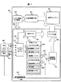
図3は本発明の階調電圧生成回路の構成図である。301はガンマ特性を調整するための設定値を保持する制御レジスタ、302は階調電圧生成回路、303は表示データに合わせた階調電圧をデコードするデコード回路である。ここで制御レジスタ301は上記振幅調整レジスタ304、傾き調整レジスタ305、微調整レジスタ306を含んだ構成である。
FIG. 3 is a block diagram of the gradation voltage generation circuit of the present invention.
また階調電圧生成回路302は、外部から供給される基準電圧316とGND間から各階調電圧を生成するラダー抵抗307、このラダー抵抗307を構成する可変抵抗321〜324、及びその可変抵抗にて抵抗分割された電圧をさらに抵抗分割するための抵抗分割回路326〜331、この抵抗分割回路326〜331で生成された階調電圧を微調整レジスタ306の設定値により選択するセレクタ回路308〜313、その各セレクタ回路の出力電圧をバッファリングするアンプ回路314及び、そのアンプ回路314出力電圧を所望の階調数分(ここでは例とし、64階調電圧)の階調電圧に抵抗分割する出力部ラダー抵抗315により構成される。
The gradation
ここでラダー抵抗307の下側に設置されている下側可変抵抗321は、振幅調整レジスタ304の下側可変抵抗設定値317により、その抵抗値を設定できる構成とし、ラダー抵抗307の上側に設置されている上側可変抵抗322は、振幅調整レジスタ304の上側可変抵抗設定値318により、その抵抗値を設定できる構成とする。この両可変抵抗321,322により抵抗分割された電圧を階調番号の両端の階調電圧とし、階調電圧の振幅調整を振幅調整レジスタ304で設定できる構成とする。
Here, the lower
またラダー抵抗307の中間部下段に設置されている中間部下側可変抵抗323は、傾き調整レジスタ305の中間部下側可変抵抗設定値319により、その抵抗値を設定できる構成とし、ラダー抵抗307中間部上側に設置されている中間部上側可変抵抗324は、傾き調整レジスタ305の中間部上側可変抵抗設定値320により、その抵抗値を設定できる構成とする。この両可変抵抗323,324により抵抗分割された電圧を中間調部の傾き特性を決めている階調番号の階調電圧とし、階調電圧の傾き特性を傾き調整レジスタ305で設定できる構成とする。
Further, the intermediate lower
上述のようなラダー抵抗構成とし、振幅調整レジスタ304、傾き調整レジスタ305により、ラダー抵抗内の可変抵抗値を設定することで抵抗分割比を変化させ、階調電圧の振幅電圧、及び中間調部の傾き特性を調整可能とする。(詳細作用については後に記述。)
また、振幅調整レジスタ304、傾き調整レジスタ305でそれぞれ設定された可変抵抗値により生成された階調電圧間を、抵抗分割回路326〜331によりさらに細かく抵抗分割し、階調電圧を微調整するための微調整用階調電圧を生成する。次に、この微調整用階調電圧を各セレクタ回路308〜313で、微調整レジスタ306の設定値325により、所望の階調電圧を選択する。この構成により、各階調電圧を微調整可能とし、ガンマ特性の調整精度を高め、調整の自由度も向上する(詳細作用は後に記述)。
The ladder resistor configuration as described above is used, and the resistance division ratio is changed by setting a variable resistance value in the ladder resistor by the
Further, in order to finely adjust the gradation voltage by further finely dividing the resistance between the gradation voltages generated by the variable resistance values respectively set by the
ここで、上述より生成される各階調電圧は後段のアンプ回路314でバッファリングされ、所望の64階調の電圧を生成するため、出力部ラダー抵抗315で、その各階調電圧間を電圧関係がリニアとなるよう抵抗分割し、64階調分の階調電圧を生成する。これにより階調電圧生成回路302で生成された64階調の階調電圧は、デコード回路303で、表示データに合わせた階調電圧をデコードし、液晶パネルへの印加電圧となる。
Here, each gradation voltage generated from the above is buffered by the
以上のような回路構成により、ガンマ特性の調整において、振幅レジスタ304、傾きレジスタ305の設定で、階調電圧の振幅電圧、及び中間調部の傾き特性といった大まかな階調電圧を調整可能なラダー抵抗を含み、そのラダー抵抗にて生成された階調電圧間から微調整レジスタ306の設定でさらに各階調電圧の微調整を行える構成とすることで、ガンマ特性の調整を容易かつ、調整時間を短縮でき、調整の精度及び自由度を向上させることで高画質化かつ、汎用性が望める階調電圧生成回路を小回路規模、低コストで実現した。
With the circuit configuration as described above, in the adjustment of the gamma characteristic, a ladder that can adjust rough gradation voltages such as the amplitude voltage of the gradation voltage and the inclination characteristic of the halftone portion by setting the
次に、本実施形態で使用した図3の可変抵抗321〜324について、レジスタ設定値と可変抵抗の動作について、図4を用いて説明する。図4において、401は上記可変抵抗321〜324の内部構成を示したものである。ここでは、レジスタ(上記振幅調整レジスタ304、及び傾き調整レジスタ305)の設定値が1減少するごとに抵抗値が4R(R:単位抵抗値)増加するといった場合の可変抵抗の構成例である。ここで、402のようにレジスタ設定値が“111”[BIN]という設定値であった場合、可変抵抗401内部の抵抗端に設置されたスイッチ403〜405はスイッチONとなり、可変抵抗401内部は短絡状態となる。よってこの時の可変抵抗401のトータル抵抗値は0Rとなる。尚ここで、各スイッチ403〜405はレジスタのbit毎に制御され、スイッチ403はレジスタ設定値の[2]bit目、スイッチ404はレジスタ設定値の[1]bit目、スイッチ405はレジスタ設定値の[0]bit目で、それぞれスイッチON、又はOFFの制御をする。次に406のようにレジスタ設定値が“000”[BIN]という設定値であった場合、可変抵抗401内部の抵抗端に設置されたスイッチ403〜405はスイッチOFFとなり、可変抵抗401のトータル抵抗値は内部抵抗値の総和となる、トータル抵抗値は28Rとなる。ここで上記構成におけるレジスタ設定値と可変抵抗値との関係は407に示した関係となる。
Next, with respect to the
尚、上記で示したレジスタ設定値と可変抵抗値との関係は一設定例であり、レジスタ設定値の各bitを反転させた場合、上記レジスタ設定値と可変抵抗値との関係は逆になり、レジスタ設定値が増加すれば可変抵抗の抵抗値も増加するという関係となる。このようにレジスタ設定値と可変抵抗値との関係を逆にした場合でも構わない。またレジスタ設定値における可変抵抗値の変化割合を、1設定値毎に4Rとしているがこの値を小さくしたり、大きくしたりしても構わない。ここで、このレジスタ設定毎の抵抗値変化割合を小さくした場合、精度は向上するが調整範囲は狭くなり、逆に大きくした場合、調整範囲は広くなるが調整精度は悪化する。また、上記で使用した単位抵抗Rは数十kΩで構成することが望ましい(消費電流を少なくできる)。また上記レジスタ設定bit数は3bitとしているがこの設定bit数を増加しても構わない。この場合、可変抵抗値の調整範囲は広くなるが回路規模は増加する。 The relationship between the register setting value and the variable resistance value shown above is an example of setting, and when each bit of the register setting value is inverted, the relationship between the register setting value and the variable resistance value is reversed. As the register setting value increases, the resistance value of the variable resistor also increases. In this way, the relationship between the register setting value and the variable resistance value may be reversed. Further, the change rate of the variable resistance value in the register set value is 4R for each set value, but this value may be reduced or increased. Here, when the resistance value change rate for each register setting is reduced, the accuracy is improved, but the adjustment range is narrowed. Conversely, when the resistance value is increased, the adjustment range is widened but the adjustment accuracy is deteriorated. Further, it is desirable that the unit resistor R used above is composed of several tens of kΩ (current consumption can be reduced). The number of register setting bits is 3 bits, but the number of setting bits may be increased. In this case, the adjustment range of the variable resistance value becomes wide, but the circuit scale increases.
以上の構成により、レジスタ設定で可変抵抗の抵抗値を変化させることが可能である。 With the above configuration, the resistance value of the variable resistor can be changed by register setting.
次に図3の振幅調整レジスタ304とラダー抵抗307内の可変抵抗321、322によるガンマ特性の調整作用について、図5を用いて説明する。
Next, the gamma characteristic adjustment operation by the
図5(a)は、図3のラダー抵抗307の下側可変抵抗321を振幅調整レジスタ304で設定した場合の調整作用を示したものである。501は振幅調整レジスタ304がデフォルト設定とした場合の階調番号−階調電圧特性である。ここで、502のように階調電圧の高い側の電圧値は変化させずに、低い側の電圧値を変化させ、階調電圧の振幅電圧を小さく調整したい場合、振幅調整レジスタ304の設定を下側可変抵抗321の抵抗値が大となるように設定すれば良い。また503のように階調電圧の高い側の電圧値は変化させずに、低い側の電圧値を変化させ、階調電圧の振幅電圧を大きく調整したい場合、振幅調整レジスタ304の設定を下側可変抵抗321の抵抗値が小となるように設定すれば良い。
FIG. 5A shows the adjustment operation when the lower
このように振幅調整レジスタ304の設定で下側可変抵抗321の抵抗値を変化させることにより、階調電圧の高い側の電圧値は変化させずに、低い側の電圧値を変化させ、階調電圧の振幅電圧を調整することが可能である。
By changing the resistance value of the lower
次に同図5の(b)は、図3のラダー抵抗307の上側可変抵抗322を振幅調整レジスタ304で設定した場合の調整作用を示したものである。501は上記同様、振幅調整レジスタ304がデフォルト設定とした場合の階調番号−階調電圧特性である。ここで、504のように階調電圧の低い側の電圧値は変化させずに、高い側の電圧値を変化させ、階調電圧の振幅電圧を小さく調整したい場合、振幅調整レジスタ304の設定を上側可変抵抗322の抵抗値が大となるように設定すれば良い。また505のように階調電圧の低い側の電圧値は変化させずに、高い側の電圧値を変化させ、階調電圧の振幅電圧を大きく調整したい場合、振幅調整レジスタ304の設定を上側可変抵抗322の抵抗値が小となるように設定すれば良い。
Next, FIG. 5B shows the adjusting action when the upper
このように振幅調整レジスタ304の設定で上側可変抵抗322の抵抗値を変化させることにより、階調電圧の低い側の電圧値は変化させずに、高い側の電圧値を変化させ、階調電圧の振幅電圧を調整することが可能である。
Thus, by changing the resistance value of the upper
次に同図5の(c)は、上述した下側可変抵抗321、上側可変抵抗322を振幅調整レジスタ304で同時に設定した場合の調整作用を示したものである。501は上記同様、振幅調整レジスタ304がデフォルト設定とした場合の階調番号−階調電圧特性である。ここで、506のように階調番号−階調電圧特性、振幅電圧は501同様とし、上下の階調電圧値を高くしたい場合、振幅調整レジスタ304の設定を下側可変抵抗321の抵抗値を大、上側可変抵抗322の抵抗値を小に設定すれば良い。また507のように階調番号−階調電圧特性、振幅電圧は501同様とし、上下の階調電圧値を低くしたい場合、振幅調整レジスタ304の設定を下側可変抵抗321の抵抗値を小、上側可変抵抗322の抵抗値を大に設定すれば良い。
Next, FIG. 5C shows the adjustment operation when the lower
このように振幅調整レジスタ304の設定で下側及び上側可変抵抗321、322を同時に設定した場合、振幅調整レジスタ304のデフォルト設定とした場合の階調番号−階調電圧特性にオフセット調整した特性となる。
In this way, when the lower and upper
以上のことにより、図3の振幅調整レジスタ304により、液晶パネル個々の特性に合わせた階調電圧の振幅電圧を調整できる。 As described above, the amplitude voltage of the gradation voltage can be adjusted according to the characteristics of each liquid crystal panel by the amplitude adjustment register 304 of FIG.
次に図3の傾き調整レジスタ305とラダー抵抗307内の可変抵抗323、324によるガンマ特性の調整作用について、図6を用いて説明する。
Next, the gamma characteristic adjustment operation by the
図6(a)は、図3のラダー抵抗307の中間部下側可変抵抗323を傾き調整レジスタ305で設定した場合の調整作用を示したものである。601は傾き調整レジスタ305がデフォルト設定とした場合の階調番号−階調電圧特性である。ここで、602のように階調電圧の高い側の傾き特性は変化させずに、階調電圧の低い側の電圧値を変化させ、階調電圧の中間調部の傾きが小になるように調整したい場合、傾き調整レジスタ305の設定を中間部下側可変抵抗323の抵抗値が大となるように設定すれば良い。
FIG. 6A shows an adjusting operation when the lower
また603のように階調電圧の高い側の傾き特性は変化させずに、階調電圧の低い側の電圧値を変化させ、階調電圧の中間調部の傾きが大になるように調整したい場合、傾き調整レジスタ305の設定を中間部下側可変抵抗323の抵抗値が小となるように設定すれば良い。
In addition, as in 603, without changing the slope characteristic on the higher gradation voltage side, the voltage value on the lower gradation voltage side is changed, and adjustment is made so that the slope of the halftone portion of the gradation voltage becomes large. In this case, the
このように傾き調整レジスタ305の設定で中間部下側可変抵抗323の抵抗値を変化させることにより、階調電圧の高い側の傾き特性は変化させずに、階調電圧の低い側の電圧値を変化させ、階調電圧の中間調部の傾きを調整することが可能である。
In this way, by changing the resistance value of the intermediate lower
次に同図6の(b)は、図3のラダー抵抗307の中間部上側可変抵抗324を傾き調整レジスタ305で設定した場合の調整作用を示したものである。601は上記同様、傾き調整レジスタ305がデフォルト設定とした場合の階調番号−階調電圧特性である。ここで、604のように階調電圧の低い側の傾き特性は変化させずに、階調電圧の高い側の電圧値を変化させ、階調電圧の中間調部の傾きが小になるように調整したい場合、傾き調整レジスタ305の設定を中間部上側可変抵抗324の抵抗値が大となるように設定すれば良い。また605のように階調電圧の低い側の傾き特性は変化させずに、階調電圧の高い側の電圧値を変化させ、階調電圧の中間調部の傾きが大になるように調整したい場合、傾き調整レジスタ305の設定を中間部上側可変抵抗324の抵抗値が小となるように設定すれば良い。
Next, FIG. 6B shows an adjustment operation when the middle upper variable resistor 324 of the
このように傾き調整レジスタ305の設定で中間部上側可変抵抗324の抵抗値を変化させることにより、階調電圧の高い側の電圧値を変化させ、階調電圧の中間調部の傾きを調整することが可能である。
In this way, by changing the resistance value of the intermediate upper variable resistor 324 according to the setting of the
次に同図6の(c)は、上述した中間部下側可変抵抗323、中間部上側可変抵抗324を傾き調整レジスタ305で同時に設定した場合の調整作用を示したものである。601は上記同様、傾き調整レジスタ305がデフォルト設定とした場合の階調番号−階調電圧特性である。ここで、606のように傾き特性は601同様とし、この傾き特性を決める階調電圧608の階調電圧値を高くしたい場合、傾き調整レジスタ305の設定を中間部下側可変抵抗323の抵抗値を大、中間部上側可変抵抗324の抵抗値を小に設定すれば良い。また607のように傾き特性は601同様とし、この傾き特性を決める階調電圧608の階調電圧値を低くしたい場合、傾き調整レジスタ305の設定を中間部下側可変抵抗323の抵抗値を小、中間部上側可変抵抗324の抵抗値を大に設定すれば良い。
Next, FIG. 6C shows the adjustment operation when the above-described intermediate lower
このように傾き調整レジスタ305の設定で中間部下側及び中間部上側可変抵抗323、324を同時に設定した場合、傾き調整レジスタ305のデフォルト設定とした場合の階調番号−階調電圧特性の傾き特性は同様とし、この傾き特性を決める階調電圧608の階調電圧値を調整した特性となる。
As described above, when the intermediate lower and upper
以上のことにより、図3の傾き調整レジスタ305により、液晶パネル個々の特性に合わせた階調電圧の振幅電圧は変えず、中間調部の傾き特性のみを調整できる。
As described above, the
次に本実施形態で使用した図3のセレクタ回路308〜313について、微調整レジスタ306の設定値とセレクタ回路308〜313との関係を図7を用いて説明する。
Next, regarding the
図7において、701は上記セレクタ回路308〜313の内部構成を示したものである。ここで702は、図3のラダー抵抗307内の抵抗分割回路326〜331の内部構成を示したものであり、ここでは例として、抵抗値1Rで抵抗分割し、8つの微調整用階調電圧A〜Hを生成する場合の構成を示している。セレクタ回路701は、この抵抗分割回路702で生成された各微調整用階調電圧A〜Hのうち1階調電圧を微調整レジスタ306の設定値703により、選択する。
In FIG. 7, reference numeral 701 denotes an internal configuration of the
上記セレクタ回路701は2to1(2入力1出力)セレクタ回路で構成されており、レジスタ設定値703の[0]bit目で1段目のセレクタ回路群704の出力を選択し、[1]bit目で2段目のセレクタ回路群705の出力を選択し、[2]bit目で3段目のセレクタ回路706の出力を選択する。
The selector circuit 701 is composed of a 2to1 (2-input 1-output) selector circuit, selects the output of the first-stage
ここでレジスタ設定値703が“000”[BIN]と設定した場合、セレクタ回路701は抵抗分割回路702で分圧された微調整用階調電圧Aを出力する。次にレジスタ設定値703が“111”[BIN]と設定した場合、セレクタ回路701は抵抗分割回路702で分圧された微調整用階調電圧Hを出力する。このようにセレクタ回路701は、微調整レジスタ306のレジスタ設定値703が1増加するごとに、抵抗分割回路702で分圧された微調整用階調電圧をAからHへと順々に選択する。このレジスタ設定値703とセレクタ回路701で選択される微調整用階調電圧A〜Hとの関係を707に示す。
When the register set
尚、上記で示したレジスタ設定値とセレクタ回路との関係は一設定例であり、レジスタ設定値の各bitを反転させた場合、上記レジスタ設定値とセレクタ回路との関係は逆になり、レジスタ設定値が増加すればセレクタ回路は微調整用階調電圧HからAへと順々に選択する。このようにレジスタ設定値と可変抵抗値との関係を逆にした場合でも構わない。 The relationship between the register setting value and the selector circuit described above is an example of setting. When each bit of the register setting value is inverted, the relationship between the register setting value and the selector circuit is reversed. When the set value increases, the selector circuit sequentially selects from the fine adjustment gradation voltage H to A. In this way, the relationship between the register setting value and the variable resistance value may be reversed.
また、上記セレクタ回路はレジスタ設定bit数は3bitとし、8つの微調整用階調電圧から1階調電圧を選択するものであるが、この設定bit数を増加して、選択できる階調数を増やしても構わない。この場合、階調電圧の微調整範囲は広くなるが回路規模は増加する。また抵抗分割回路内部の抵抗値を1Rとしているがこの値を小さくしたり、大きくしたりしても構わない。この抵抗分割回路内部の抵抗値を小さくした場合、微調整範囲は狭くなるが調整精度は向上する。また抵抗分割回路内部の抵抗値を大きくした場合、微調整範囲は広くなるが調整精度は悪化する。また、図4の可変抵抗構成と同様、単位抵抗Rは数十kΩで構成することが望ましい(消費電流を少なくできる)。 The selector circuit sets the number of register setting bits to 3 bits and selects one gradation voltage from eight fine adjustment gradation voltages. By increasing the number of setting bits, the number of gradations that can be selected is increased. You can increase it. In this case, the fine adjustment range of the gradation voltage is widened, but the circuit scale is increased. Further, although the resistance value inside the resistance dividing circuit is 1R, this value may be reduced or increased. When the resistance value in the resistance dividing circuit is reduced, the fine adjustment range is narrowed but the adjustment accuracy is improved. Further, when the resistance value inside the resistance dividing circuit is increased, the fine adjustment range is widened, but the adjustment accuracy is deteriorated. Further, like the variable resistance configuration of FIG. 4, it is desirable that the unit resistance R be configured with several tens of kΩ (current consumption can be reduced).
次に図3の微調整レジスタ306とセレクタ回路308〜313によるガンマ特性の調整作用について、図8を用いて説明する。
Next, the gamma characteristic adjustment operation by the
図8において、801は微調整レジスタ306がデフォルト設定とした場合の階調番号−階調電圧特性である。また802は微調整レジスタ306の設定値をセレクタ回路308〜313で選択される電圧値が最大となるよう設定した場合の特性図である。803は微調整レジスタ306の設定値をセレクタ回路308〜313で選択される電圧値が最小となるよう設定した場合の特性図である。よって、上記802と803の間の電圧が微調整レジスタ306で設定できる微調整可能な階調電圧範囲である。ここで804〜809はセレクタ回路308〜313の出力(微調整可能な階調電圧)を示しておりそれぞれ、上記802と803の間の階調電圧範囲内で微調整可能である。
In FIG. 8,
以上のように図3の微調整レジスタ306の設定により、ラダー抵抗307内の抵抗分割回路326〜331で生成された各微調整用階調電圧から1階調電圧を選択し、微調整可能とする。これにより、液晶パネル個々の特性に合わせた階調電圧の微調整可能とし、調整精度を向上することで高画質化が望める。
As described above, by setting the
上述で説明した振幅、傾き、微調整の3種類の調整レジスタを用いて、ガンマ特性を調整できる階調電圧生成回路を信号線駆動回路内に組み込んだ場合の液晶表示装置システム構成例を図9に示す。ここで図中の900は本発明の液晶表示装置であり、901は液晶パネルであり、902は液晶パネル901の信号線に表示データに対応した階調電圧を出力する図3の階調電圧生成回路302を含んだ信号線駆動回路であり、903は液晶パネル901の走査ラインを走査する走査線駆動回路であり、904は上記信号線駆動回路902、走査線駆動回路903の動作電源を供給するシステム電源生成回路である。ここで、このシステム電源生成回路904から信号線駆動回路902に供給される電源電圧905内に図3の基準電圧316が含まれる。次に、906は液晶パネル901に画像を表示させるための各種制御及び各種処理を行うMPU(マイクロプロセッサユニット)であり、信号線駆動回路902は、このMPU906との表示データ並びに制御レジスタのデータのやりとりを行うシステムインターフェース907、システムインターフェース907より出力される表示データ908を一時保存しておくための表示メモリ909、及び図3で示した制御レジスタ301、階調電圧生成回路302、デコード回路303で構成される。尚、制御レジスタ301内部は図3でも示した振幅調整レジスタ304、傾き調整レジスタ305、微調整レジスタ306を含む。
FIG. 9 shows an example of the configuration of a liquid crystal display device system when a gradation voltage generation circuit capable of adjusting gamma characteristics using the three types of adjustment registers of amplitude, inclination, and fine adjustment described above is incorporated in a signal line driver circuit. Shown in Here, 900 in the figure is the liquid crystal display device of the present invention, 901 is the liquid crystal panel, 902 is the gradation voltage generation of FIG. 3 that outputs the gradation voltage corresponding to the display data to the signal line of the
上記MPU906は、例えば汎用MPUである68系16bitのバスインタフェースに準拠しており、チップ選択を示すCS(chip Select)信号、制御レジスタ301のアドレスを指定するのかデータを指定するのかを選択するRS(Register Select)信号、処理動作の起動を指示するE(Enable)信号、データの書込みまたは読出しを選択するR/W(Read/Write)信号、制御レジスタ301のアドレスまたはデータの実際の設定値である16bitのData信号で構成される。これらの制御信号により、制御レジスタ301の各アドレスに対し、振幅調整レジスタ304、傾き調整レジスタ305、微調整レジスタ306のレジスタ設定値が割振られ、制御レジスタ301のレジスタ内に設定データを各割り当てられたアドレスごと書き込み、又は読み出し動作を行う。
The
次に図10を用いてこのMPU906と信号線駆動回路902内部のインターフェース907間における各制御信号の動作について説明する。 まず、CS信号を“ロー”とし、制御レジスタ301をアクセス可能状態とする。RS信号を“ロー”時にはアドレス指定期間を意味し、RS信号“ハイ”時にはデータ指定期間を意味する。ここで制御レジスタ301への書き込み動作を行う場合、R/W信号を“ロー”とし、先のアドレス指定期間にData信号に所定のアドレス値を設定し、データ指定期間にそのアドレスのレジスタに書き込むデータ(上述での振幅調整レジスタ304、傾き調整レジスタ305、微調整レジスタ306のレジスタ設定値等々)を設定する。その設定後E信号を一定期間“ハイ”にすることで制御レジスタ301にデータを書き込む。
Next, the operation of each control signal between the
また制御レジスタ301に設定されたデータを読み出す際には、上記と同様にCS、RS信号を設定し、R/W信号を“ハイ”とし、アドレス期間に所定のアドレスを設定し、上記同様、設定後E信号を一定期間“ハイ”とすることで、データ指定期間にレジスタ内に書き込まれたデータが読み出される。
Further, when reading the data set in the
以上、制御レジスタ301のレジスタ内の各割り当てられたアドレスに振幅調整レジスタ304、傾き調整レジスタ305、微調整レジスタ306のレジスタ設定値を書き込み動作を行うことで、上述したガンマ特性の調整において、上記各レジスタによる階調電圧の振幅電圧調整、中間調部の傾き特性調整、微調整が可能となり、ガンマ特性の調整が容易となり、また液晶パネル個々の特性に合わせた階調電圧を設定可能とする。
As described above, in the adjustment of the gamma characteristic described above, the register setting values of the
次に、本発明の第2の実施形態による液晶表示装置の構成について説明する。 Next, the configuration of the liquid crystal display device according to the second embodiment of the present invention will be described.
まず、一般的に液晶パネルに階調電圧を印加する場合には、ある一定周期の交流信号(以下Mと称す。)で階調電圧を反転させて、液晶パネルを交流化駆動しなければならない。 First, in general, when a gradation voltage is applied to a liquid crystal panel, it is necessary to invert the gradation voltage with an AC signal (hereinafter referred to as M) having a certain period to drive the liquid crystal panel in an alternating current. .
ここで液晶パネルの階調番号−階調電圧特性も、上記Mの極性ごとで異なり、そのMの極性ごとに、所望のガンマ特性に調整しなければならないケースがある。ここで図11に液晶パネルの交流化における階調番号−階調電圧特性の変化について示す。1101は、正極性(Mの極性がM=0)時の階調番号−階調電圧特性である。ここで液晶パネルがノーマリーブラックモードの場合、階調番号が大きくなるにつれ、階調電圧は高くなるという特性を示している。1102は、負極性(Mの極性がM=1)時の階調番号−階調電圧特性である。ここで階調番号が大きくなるにつれ、階調電圧は低くなるという特性を示している。ここで1101と1102は、センタライン1103を軸とし対称の関係となっている。このように正極性、あるいは負極性の階調番号−階調電圧特性が対称の関係であれば、前記した第1の実施形態による図3の階調電圧生成回路構成において、64階調電圧の出力関係を反転(64階調目の階調電圧を1階調目の階調電圧とし、1階調目の階調電圧を64階調目の階調電圧と階調電圧と階調番号の関係を反転)すれば、正/負両極性においてガンマ特性の調整を行う必要は無い。しかし、液晶パネルによっては1104のような正/負極性で異なった階調番号−階調電圧特性となるケースがある。この場合、図3の第1の実施形態による階調電圧生成回路構成では、所望のガンマ特性に調整するため、正/負極性の特性に応じ随時レジスタ設定を行わなければならない。そこで上記問題を解決するため、本第2の実施形態では、第1の実施形態同様の作用があるラダー抵抗を正極性用、負極性用に独立して具備し、ガンマ特性の調整を正/負両極性で行える構成とした。
Here, the gradation number-gradation voltage characteristics of the liquid crystal panel are also different for each of the M polarities, and there are cases where the desired gamma characteristics must be adjusted for each of the M polarities. Here, FIG. 11 shows changes in gradation number-gradation voltage characteristics when the liquid crystal panel is switched to AC.
本発明の第2の実施形態による液晶表示装置の構成について図12を用いて説明する。 The configuration of the liquid crystal display device according to the second embodiment of the present invention will be described with reference to FIG.
図12は、前記第1の実施形態における図3の階調電圧生成回路302の内部構成のみを変更したものである。尚、制御レジスタ301やデコード回路303の構成及び動作については第1の実施形態と同様である。ここで図12の階調電圧生成回路302は、第1の実施形態における図3のラダー抵抗307を正極性用ラダー抵抗1202、及び負極性用ラダー抵抗1203と正/負極性毎に独立して2本具備した構成としている。
FIG. 12 is a diagram in which only the internal configuration of the gradation
尚、この正/負極性用ラダー抵抗1202、1203は、第1の実施形態同様の作用を振幅調整レジスタ304、傾き調整レジスタ305のレジスタ設定により行える構成とする。
The positive / negative
ここで、この正/負両極性用ラダー抵抗1202、1203は、上記調整レジスタ304、305の設定値を共用し、その設定値により第1の実施形態同様に階調電圧の振幅電圧の調整、及び特性傾きの調整を正/負極性毎に行える構成とする。ここで、正極性用ラダー抵抗1202内部の抵抗値設定と負極性用ラダー抵抗1203内部抵抗値設定は上記調整レジスタ304、305の同設定で正極性、負極性で異なった階調電圧調整が行えるように異なった抵抗値設定とする。
Here, the positive / negative
また上記のように正/負極性用ラダー抵抗1202、1203を2本具備することにより、図3におけるセレクタ回路308〜313も正極性用セレクタ回路1204と負極性用セレクタ回路1205の2種類必要となる。ここで、正/負両極性用セレクタ回路1204、1205は、第1の実施形態である図3のセレクタ回路308〜313と同構成とし、微調整レジスタ306設定により、第1の実施形態と同作用の微調整を可能とする。
Further, by providing two positive /
上記のような構成とし、M信号にて選択する極性セレクタ回路1201、1206により、正/負極性用ラダー抵抗1202、1203及び正/負極性用セレクタ回路1204、1205出力をMの極性により選択する。尚、上記極性セレクタ1201、1206はM=0時には正極性用ラダー抵抗1202、及び正極性用セレクタ回路1204出力を選択し、M=1時には負極性用ラダー抵抗1203、及び負極性用セレクタ回路1205出力を選択する。
With the configuration as described above, the
以上のような階調電圧生成回路構成とし、第1の実施形態における図9同様の液晶表示装置システムに組み込むことで、正/負両極性のガンマ特性を独立して調整できる液晶表示装置を実現した。尚、各調整レジスタ304〜306の設定値は、第1の実施形態と同様に図10の制御信号により、制御レジスタ301内のアドレスにそれぞれ割り当て、各レジスタ設定値の書き込み動作を行うこととする。
A gray-scale voltage generation circuit configuration as described above is incorporated into the liquid crystal display device system similar to that of FIG. 9 in the first embodiment, thereby realizing a liquid crystal display device that can independently adjust positive / negative gamma characteristics. did. Note that the setting values of the respective adjustment registers 304 to 306 are assigned to the addresses in the
次に第3の実施形態による階調電圧生成回路構成を図13に示す。ここで本実施形態は、上述第2の実施形態で2本構成としていたラダー抵抗を1本構成とし、第1の実施形態における振幅、傾き、微調整レジスタといった各調整レジスタを正/負極性独立させ具備し、正/負両極性のガンマ特性を独立して調整できるようにしたものである。ここで図13は図3の第1の実施形態である階調電圧生成回路において、制御レジスタ301の内部構成のみを変更したものである。よって階調生成回路302やデコード回路303などの構成及び動作については前述第1の実施形態と同様である。ここで図13の制御レジスタ301の内部について、1301は正極性用振幅調整レジスタ、1302は負極性用振幅調整レジスタ、1303は正極性用傾き調整レジスタ、1304は負極性用傾き調整レジスタ、1305は正極性用微調整レジスタ、1306は負極性用微調整レジスタであり、それぞれ正/負両極性で独立して設定できるものとする。これら調整レジスタ1301〜1306はM信号により選択するセレクタ回路1307〜1309により、正/負極性に応じたレジスタ1301〜1306の設定値を選択する。ここでこのセレクタ回路1307〜1309は、M=0時には正極性用レジスタ1301、1303、1305の設定値を選択し、M=1時には負極性用レジスタ1302、1304、1306の設定値をそれぞれ選択する。ここで正/負極性用振幅調整レジスタ1301、1302は図5で示した第1の実施形態による振幅調整レジスタと同等の作用が得られ、正/負極性用傾き調整レジスタ1303、1304は図6で示した傾き調整レジスタと同等の作用が得られ、正/負極性用微調整レジスタ1305、1306は図8で示した微調整レジスタと同等の作用が得られる。
Next, FIG. 13 shows a grayscale voltage generation circuit configuration according to the third embodiment. Here, in this embodiment, the ladder resistor, which has been configured in two in the second embodiment, is configured as one, and each adjustment register such as the amplitude, inclination, and fine adjustment register in the first embodiment is independent of positive / negative polarity. The gamma characteristics of both positive and negative polarities can be adjusted independently. Here, FIG. 13 shows only the internal configuration of the
よって上述した正/負極性用調整レジスタ1301〜1306により、正/負極性において、第1の実施形態と同様作用が得られることにより、液晶パネル個々の特性に合った階調電圧、及びガンマ特性の調整を、正/負両極性とも独立に調整できる構成とした。 Therefore, the positive / negative polarity adjustment registers 1301 to 1306 described above provide the same operation as that of the first embodiment in the positive / negative polarity, so that the gradation voltage and the gamma characteristic suitable for the individual characteristics of the liquid crystal panel are obtained. In this configuration, both positive and negative polarities can be adjusted independently.
以上のような制御レジスタ301構成を図14の液晶表示装置システムに組み込むことで、第2の実施形態よりも小回路規模で正/負両極性のガンマ特性を独立して調整できる液晶表示装置を実現した。尚、正/負極性用調整レジスタ1301〜1306の設定値は、図10と同様の制御信号により、制御レジスタ301内のアドレスに正/負極性用調整レジスタ1301〜1306をそれぞれ割り当て、各レジスタ設定値の書き込み動作を行うこととする。
By incorporating the configuration of the control register 301 as described above into the liquid crystal display device system of FIG. 14, a liquid crystal display device capable of independently adjusting the positive / negative bipolar gamma characteristics with a smaller circuit scale than the second embodiment. It was realized. The set values of the positive / negative polarity adjustment registers 1301 to 1306 are assigned to the addresses in the
次に、本発明の第4の実施形態による液晶表示装置の構成について説明する。 Next, the configuration of the liquid crystal display device according to the fourth embodiment of the present invention will be described.
液晶パネルはその使用用途によって、バックライトを当てて画像を表示させる場合があり、この場合このバックライトON、又はOFFにより液晶パネルの階調番号−階調電圧特性が変化するケースもあり、ガンマ特性の調整も行う必要がある。本実施形態では、上述のようなバックライトON/OFF時におけるガンマ特性の調整方法について、図15を用いて説明する。 A liquid crystal panel may display an image with a backlight depending on its usage. In this case, the gradation number-gradation voltage characteristics of the liquid crystal panel may change depending on whether the backlight is turned on or off. It is also necessary to adjust the characteristics. In the present embodiment, a gamma characteristic adjustment method at the time of backlight ON / OFF as described above will be described with reference to FIG.
図15は図9の第1の実施形態における液晶表示装置システム構成図において、MPU906及び信号線駆動回路902内の制御レジスタ301内部を変更したものであり、他ブロックの構成、及び動作については第1の実施形態同様である。但し、液晶パネル901は上述のバックライト回路を含むものとする。ここで、MPU906内部には上記バックライトON/OFFを判別するバックライトON/OFF判別手段1401を設け、制御レジスタ301には、前記第1の実施形態と同様の作用を持つ、振幅調整レジスタ304、傾き調整レジスタ305、微調整レジスタ305を含んだバックライトON時のレジスタ1402と上記同レジスタを含む、バックライトOFF時レジスタ1403とを独立して具備する。ここで先のバックライトON/OFF判別手段1401から出力されるバックライトONあるいはバックライトOFF状態を示す判別信号1404により、上記バックライトON時レジスタ1402とバックライトOFF時レジスタ1403の設定値をセレクタ回路1405で選択し、このセレクタ回路1405で選択されたレジスタ設定値を第1の実施形態と同構成である階調電圧生成回路302内で使用する。
FIG. 15 is a configuration diagram of the liquid crystal display device system according to the first embodiment shown in FIG. 9 in which the
以上のように制御レジスタ301内に第1の実施形態と同様の作用を持つ振幅、傾き、微調整レジスタをバックライトON時、及びバックライトOFF時用に2種類具備する構成とすることにより、バックライトON/OFFによる液晶パネル個々の特性におけるガンマ特性の調整についても、個別に調整でき、高画質化が望める液晶表示装置を実現した。尚、バックライトON時のレジスタ1402、及びバックライトOFF時レジスタ1403の設定値は、第1の実施形態と同様に図10の制御信号により、制御レジスタ301内のアドレスにそれぞれ割り当て、各レジスタ設定値の書き込み動作を行うこととする。
As described above, the
次に、本発明の第5の実施形態による液晶表示装置の構成について説明する。 Next, the configuration of the liquid crystal display device according to the fifth embodiment of the present invention will be described.
本実施形態は、液晶パネルの表示色である赤、緑、青(以下R、G、Bと称す。)ごとにガンマ特性を個別に調整できるようにしたものであり、その構成について図16を用いて説明する。 In this embodiment, the gamma characteristic can be individually adjusted for each of red, green, and blue (hereinafter referred to as R, G, and B) that are display colors of the liquid crystal panel. It explains using.
図16は第4の実施形態の図15同様、図9の第1の実施形態における液晶表示装置システム構成図において、制御レジスタ301の内部構成のみを変更したものであり、他ブロックの構成、及び動作については第1の実施形態同様である。ここで上記R、G、Bのガンマ特性を個別に調整するため、制御レジスタ301内に、R用調整レジスタ1601、G用調整レジスタ1602、B用調整レジスタ1603を独立して具備する構成とした。ここで上記調整レジスタ1601〜1602はいずれも、第1実施形態と同様の作用が得られる振幅調整レジスタ304、傾き調整レジスタ305、微調整レジスタ306を含む。
以上のように、制御レジスタ301内に第1の実施形態と同様の作用を持つ振幅、傾き、微調整レジスタを含む、R用、G用、B用調整レジスタ1601〜1603といった液晶パネルの表示色毎に独立してレジスタ具備する構成とすることにより、液晶パネルの表示色R、G、B各色のガンマ特性を個別で調整可能とし、より高画質化が望める液晶表示装置を実現した。尚、R用、G用、B用調整レジスタ1601〜1603の設定値は、第1の実施形態と同様に図10の制御信号により、制御レジスタ301内のアドレスにそれぞれ割り当て、各レジスタ設定値の書き込み動作を行うこととする。
FIG. 16 is similar to FIG. 15 of the fourth embodiment, in which only the internal configuration of the
As described above, the display colors of the liquid crystal panels such as the R, G, and B adjustment registers 1601 to 1603 including the amplitude, inclination, and fine adjustment registers having the same operations as those in the first embodiment are included in the
本発明は以上に示した実施形態に限定されるものでは無く、種々の変更が可能である。例えば、上述では、液晶パネルのモードをノーマリーブラックモードを前提として説明を行ったが、本発明は上記液晶パネルのモードに関係なく実施できる。また階調数を64階調を前提として説明を行ったが、本発明は他階調数に関係なく実施可能である。 The present invention is not limited to the embodiments described above, and various modifications can be made. For example, in the above description, the mode of the liquid crystal panel has been described on the assumption of the normally black mode, but the present invention can be implemented regardless of the mode of the liquid crystal panel. Although the description has been made on the assumption that the number of gradations is 64 gradations, the present invention can be implemented regardless of the number of other gradations.
上記本発明の第1〜第5の実施形態によれば、ガンマ特性の調整において、振幅調整レジスタ、傾き調整レジスタを具備し、そのレジスタ設定により、液晶パネル個々の特性に応じた階調電圧の振幅電圧、及び中間調部の傾き特性といった大まか階調電圧を調整可能なラダー抵抗構成を具備することで、ガンマ特性の調整を容易とし、調整時間を短縮できる。また上記各調整をラダー抵抗で行えることすることで小回路規模、かつ、低コストの効果がある。 According to the first to fifth embodiments of the present invention, the adjustment of the gamma characteristic includes the amplitude adjustment register and the inclination adjustment register, and the gradation voltage corresponding to the individual characteristics of the liquid crystal panel is set by the register setting. By providing a ladder resistor configuration capable of roughly adjusting the gradation voltage such as the amplitude voltage and the gradient characteristic of the halftone part, the gamma characteristic can be easily adjusted and the adjustment time can be shortened. In addition, since each of the above adjustments can be performed with a ladder resistor, there is a small circuit scale and low cost effect.
また、振幅レジスタ、傾きレジスタに加え、微調整レジスタを具備することで、上記レジスタにて調整された階調電圧に対し、さらに微調整を行える構成とすることにより、調整精度を高め、高画質化が望める効果がある。 In addition to the amplitude register and the inclination register, a fine adjustment register is provided so that the gradation voltage adjusted by the register can be further finely adjusted, thereby improving adjustment accuracy and high image quality. There is an effect that can be expected.
また、上記本発明の第1〜第5の実施形態によれば、液晶パネル個々の特性に合わせたガンマ特性の調整が可能になるので、汎用性のある回路構成が構築できる効果がある。 Further, according to the first to fifth embodiments of the present invention, the gamma characteristic can be adjusted in accordance with the characteristics of each liquid crystal panel, so that there is an effect that a versatile circuit configuration can be constructed.
301…制御レジスタ、302…階調電圧生成回路、303…デコード回路、304…振幅調整レジスタ、305…傾き調整レジスタ、306…微調整レジスタ、307…ラダー抵抗、308〜313…セレクタ回路、314…アンプ回路、315…出力部ラダー抵抗、316…基準電圧、317…下側可変抵抗設定値、318…上側可変抵抗設定値、319…中間部下側可変抵抗設定値、320…中間部上側可変抵抗設定値、321…下側可変抵抗、322…上側可変抵抗、323…中間部下側可変抵抗、324…中間部上側可変抵抗、325…微調整レジスタ設定値、326〜331…抵抗分割回路。
DESCRIPTION OF
Claims (21)
外部から表示データを入力するためのシステムインターフェイスと、
前記表示データを格納するためのメモリと、
複数の階調電圧を生成するための階調電圧生成回路と、
前記γ特性を調整するためのγ調整回路と、
前記メモリからの前記表示データに応じた前記階調電圧を前記液晶表示パネルへ出力するための回路と、を備え、
前記階調電圧生成回路は、
第1可変抵抗と、第1抵抗分割回路と、第2可変抵抗と、複数の第2抵抗分割回路と、第3可変抵抗と、第3抵抗分割回路と、第4可変抵抗とが第1レベルの電圧と前記第1レベルの電圧と異なる第2レベルの電圧の間に直列に結合された第1のラダー抵抗と、
前記第1抵抗分割回路から引き出された複数の線から1つの線を選択することによって所望の電圧を選択するための第1セレクタ回路と、
前記複数の第2抵抗分割回路の各々から引き出された複数の線から1つの線を各々選択することによって所望の電圧を選択するための複数の第2セレクタ回路と、
前記第3抵抗分割回路から引き出された複数の線から1つの線を選択することによって所望の電圧を選択するための第3セレクタ回路と、
前記第1、第2及び第3セレクタ回路からの出力を所定の部分に受けるようにされ、前記第1可変抵抗と前記第1抵抗分割回路との間の電圧に従う第3レベルの電圧と、前記第3抵抗分割回路と前記第4可変抵抗との間の電圧に従う第4レベルの電圧との間に結合された複数の抵抗を有する第2のラダー抵抗と、を含み、
前記第2のラダー抵抗での分割により、前記複数の階調電圧を出力し、
前記γ調整回路は、
前記γ特性の振幅を調整するために、前記第1のラダー抵抗中の前記第1及び第4可変抵抗を制御するための第1の値が設定される振幅調整レジスタと、
前記γ特性の中間部分の傾きを調整するために、前記第1のラダー抵抗中の前記第2及び第3可変抵抗を制御するための第2の値が設定される傾き調整レジスタと、
前記γ特性を微調整するために、前記第1、第2及び第3セレクタ回路によって選択される各電圧を制御するための第3の値が設定される微調整レジスタとを備え、
前記振幅調整レジスタと前記傾き調整レジスタと前記微調整レジスタは、前記γ特性における正極性に対する設定値と負極性に対する設定値とを独立に設定可能であることを特徴とする表示駆動装置。 In a display driving device capable of adjusting the γ characteristic of a liquid crystal display panel,
A system interface for inputting display data from outside,
A memory for storing the display data;
A gradation voltage generation circuit for generating a plurality of gradation voltages;
A γ adjusting circuit for adjusting the γ characteristic;
A circuit for outputting the gradation voltage corresponding to the display data from the memory to the liquid crystal display panel,
The gradation voltage generation circuit includes:
The first variable resistor, the first resistor divider circuit, the second variable resistor, the plurality of second resistor divider circuits, the third variable resistor, the third resistor divider circuit, and the fourth variable resistor are at the first level. A first ladder resistor coupled in series between a second voltage different from the first level voltage and a second level voltage different from the first level voltage;
A first selector circuit for selecting a desired voltage by selecting one line from a plurality of lines drawn from the first resistance divider circuit;
A plurality of second selector circuits for selecting a desired voltage by respectively selecting one line from a plurality of lines drawn from each of the plurality of second resistance divider circuits;
A third selector circuit for selecting a desired voltage by selecting one line from a plurality of lines drawn from the third resistance divider circuit;
A third level voltage according to a voltage between the first variable resistor and the first resistor divider circuit, wherein the output from the first, second and third selector circuits is received by a predetermined portion; A second ladder resistor having a plurality of resistors coupled between a third resistor divider circuit and a fourth level voltage according to a voltage between the fourth variable resistor;
The plurality of gradation voltages are output by the division by the second ladder resistor,
The γ adjustment circuit includes:
An amplitude adjustment register in which a first value for controlling the first and fourth variable resistors in the first ladder resistor is set in order to adjust the amplitude of the γ characteristic;
An inclination adjustment register in which a second value for controlling the second and third variable resistors in the first ladder resistor is set in order to adjust an inclination of an intermediate portion of the γ characteristic;
To fine-tune the pre SL γ characteristic, a fine adjustment register the first, third value for controlling the voltages selected by the second and third selector circuit is set,
The display drive device, wherein the amplitude adjustment register, the inclination adjustment register, and the fine adjustment register can independently set a setting value for positive polarity and a setting value for negative polarity in the γ characteristic .
第1可変抵抗と、第1抵抗分割回路と、第2可変抵抗と、複数の第2抵抗分割回路と、第3可変抵抗と、第3抵抗分割回路と、第4可変抵抗とが第1レベルの電圧の接続端と前記第1レベルの電圧と異なる第2レベルの電圧の接続端の間に直列に接続された第1のラダー抵抗と、前記第1抵抗分割回路から引き出された複数の線から1つの線を選択することによって所望の電圧を選択するための第1セレクタ回路と、前記複数の第2抵抗分割回路の各々から引き出された複数の線から1つの線を各々選択することによって所望の電圧を選択するための複数の第2セレクタ回路と、前記第3抵抗分割回路から引き出された複数の線から1つの線を選択することによって所望の電圧を選択するための第3セレクタ回路と、前記第1、第2及び第3セレクタ回路からの出力を所定の部分に受けるようにされ、前記第1可変抵抗と前記第1抵抗分割回路との間の電圧に従う第3レベルの電圧と、前記第3抵抗分割回路と前記第4可変抵抗との間の電圧に従う第4レベルの電圧との間に結合された複数の抵抗を有する第2のラダー抵抗と、を含み、前記第2のラダー抵抗での分割により、複数レベルの電圧を生成するための生成回路と、
前記複数レベルの電圧の中から、前記表示データに応じた前記階調電圧をデコードするためのデコード回路と、
階調に対する階調電圧の特性曲線の振幅及び傾きを独立に調整するために、前記外部装置から受信された前記第1、第2、第3及び第4可変抵抗の値を設定するための第1及び第2の値を設定可能な第1及び第2のレジスタと、
前記特性曲線を微調整するために、前記外部装置から受信された前記第1、第2及び第3セレクタ回路により選択すべき電圧の値を設定するための第3の値を設定可能な第3のレジスタとを備え、
前記第1及び第2のレジスタの設定値により、前記第1、第2、第3及び第4可変抵抗の値が制御され、前記第3のレジスタの設定値により、前記第1、第2及び第3セレクタ回路で選択する電圧の値が制御されることを特徴とする表示駆動装置。 In a display driving device for outputting a gradation voltage corresponding to display data received from an external device to a liquid crystal display panel,
The first variable resistor, the first resistor divider circuit, the second variable resistor, the plurality of second resistor divider circuits, the third variable resistor, the third resistor divider circuit, and the fourth variable resistor are at the first level. A first ladder resistor connected in series between a connection end of the first voltage and a connection end of a second level voltage different from the first level voltage, and a plurality of lines drawn from the first resistance divider circuit By selecting one line from the first selector circuit for selecting a desired voltage by selecting one line from the plurality of lines drawn from each of the plurality of second resistance divider circuits, A plurality of second selector circuits for selecting a desired voltage, and a third selector circuit for selecting a desired voltage by selecting one line from the plurality of lines drawn from the third resistance divider circuit And the first, second and third The output from the rectifier circuit is received by a predetermined portion, and a third level voltage according to the voltage between the first variable resistor and the first resistor divider circuit, the third resistor divider circuit, and the fourth resistor anda second ladder resistor having a plurality of resistors coupled between the fourth level voltage according the voltage between the variable resistor, by cleavage with the second ladder resistance, the multiple levels A generation circuit for generating a voltage;
From among the plurality of levels of voltages, a decoding circuit for decoding the gradation voltage corresponding to the display data,
To adjust independently the amplitude and slope of the characteristic curve of the gradation voltages against the gradation, the external device said first received from, the second, for setting the third and the value of the fourth variable resistor First and second registers capable of setting first and second values ;
To fine-tune the pre-Symbol characteristic curve, wherein received from an external device first and capable of setting a third value for setting the value of the voltage to be selected by the second and third selector circuit 3 registers ,
The values of the first, second, third and fourth variable resistors are controlled by the setting values of the first and second registers, and the first, second and second values are controlled by the setting values of the third register. display driving apparatus which the value of the voltage to be selected by the third selector circuit is characterized Rukoto controlled.
前記第1のレジスタ内に設定された前記第1の値により前記特性曲線の振幅を調整するための前記第1及び第4可変抵抗の値が調整され、
前記第2のレジスタ内に設定された前記第2の値により前記特性曲線の傾きを調整するための前記第2及び第3可変抵抗の値が調整されることを特徴とする表示駆動装置。 The display driving apparatus according to claim 2,
The values of the first and fourth variable resistors for adjusting the amplitude of the characteristic curve are adjusted by the first value set in the first register ,
Display driving apparatus, characterized in that the second and the value of the third variable resistor for adjusting the inclination of the characteristic curve by the set second value in the second register is adjusted.
前記第1及び第2のレジスタは、正極性における前記特性曲線の振幅及び傾きを調整するための前記第1、第2、第3及び第4可変抵抗の値を設定するための前記第1及び第2の値と、負極性における前記特性曲線の振幅及び傾きを調整するための前記第1、第2、第3及び第4可変抵抗の値を設定するための前記第1及び第2の値とを、独立に設定可能であり、
前記第3のレジスタは、正極性における前記特性曲線の傾きを微調整するための前記第1、第2及び第3セレクタ回路により選択すべき電圧の値を設定するための前記第3の値と、負極性における前記特性曲線の傾きを微調整するための前記第1、第2及び第3セレクタ回路により選択すべき電圧の値を設定するための前記第3の値とを、独立に設定可能であることを特徴とする表示駆動装置。 The display driving apparatus according to claim 2,
The first and second registers set the first, second, third, and fourth variable resistors for adjusting the amplitude and slope of the characteristic curve in positive polarity. The second value and the first and second values for setting the values of the first, second, third and fourth variable resistors for adjusting the amplitude and slope of the characteristic curve in negative polarity And can be set independently,
The third register includes the third value for setting a voltage value to be selected by the first, second and third selector circuits for finely adjusting the slope of the characteristic curve in positive polarity. The third value for setting the voltage value to be selected by the first, second and third selector circuits for finely adjusting the slope of the characteristic curve in the negative polarity can be set independently. A display drive device characterized by the above.
前記液晶表示パネルへ出力する前記階調電圧は、交流信号に従い、正極性と負極性が反転され、
前記交流信号に応じて、前記正極性における前記特性曲線の調整のための前記第1、第2及び第3の値と、前記負極性における前記特性曲線の調整のための前記第1、第2及び第3の値とを選択して用いることを特徴とする表示駆動装置。 The display driving device according to claim 4 .
The gradation voltage to be output to the liquid crystal display panel is inverted in positive polarity and negative polarity according to an AC signal,
According to the AC signal, the first, second and third values for adjusting the characteristic curve in the positive polarity and the first and second values for adjusting the characteristic curve in the negative polarity. And a third value selected and used .
前記表示データと前記特性曲線の振幅及び傾きを調整するための前記第1、第2、第3及び第4可変抵抗の値を設定するための前記第1及び第2の値とを、前記外部装置から受信するためのインターフェースを備えることを特徴とする表示駆動装置。 The display driving apparatus according to claim 2,
The display data and the first and second values for setting the values of the first, second, third and fourth variable resistors for adjusting the amplitude and inclination of the characteristic curve, A display driving device comprising an interface for receiving from a device.
前記インターフェースは、前記特性曲線の振幅及び傾きを調整するための前記第1及び第2の値のために割り当てられた前記第1及び第2のレジスタの各アドレスを前記外部装置から受信し、前記各アドレスに連続して、前記特性曲線の振幅及び傾きを調整するための前記第1及び第2の値を前記外部装置から受信し、
前記受信した前記第1及び第2の値は、前記受信した前記各アドレスで指定される前記第1及び第2のレジスタへ設定されることを特徴とする表示駆動装置。 The display driving device according to claim 6 .
The interface receives each address of the first and second registers assigned for the first and second values for adjusting the amplitude and slope of the characteristic curve from the external device, and Continuously receiving each address, the first and second values for adjusting the amplitude and slope of the characteristic curve are received from the external device ,
The display driving device , wherein the received first and second values are set in the first and second registers specified by the received addresses .
前記生成回路は、64個のレベルの電圧を生成することを特徴とする表示駆動装置。 The display driving apparatus according to claim 2,
The display driving device, wherein the generation circuit generates voltages of 64 levels.
第1可変抵抗と、第1抵抗分割回路と、第2可変抵抗と、複数の第2抵抗分割回路と、第3可変抵抗と、第3抵抗分割回路と、第4可変抵抗とが第1レベルの電圧と第2レベルの電圧の間に直列に接続された第1のラダー抵抗と、前記第1抵抗分割回路から引き出された複数の線から1つの線を選択するための第1セレクタ回路と、前記複数の第2抵抗分割回路の各々から引き出された複数の線から1つの線を各々選択するための複数の第2セレクタ回路と、前記第3抵抗分割回路から引き出された複数の線から1つの線を選択するための第3セレクタ回路と、前記第1、第2及び第3セレクタ回路からの出力を所定の部分に受けるようにされ、前記第1可変抵抗と前記第1抵抗分割回路との間の電圧に従う第3レベルの電圧と、前記第3抵抗分割回路と前記第4可変抵抗との間の電圧に従う第4レベルの電圧との間に結合された複数の抵抗を有する第2のラダー抵抗と、を含み、前記第2のラダー抵抗での分割により、複数レベルの電圧を生成するための生成回路と、
前記複数レベルの電圧の中から、前記表示データに応じた前記階調電圧をデコードするためのデコード回路と、
階調に対する階調電圧の特性曲線の振幅及び傾きを独立に調整し前記特性曲線を微調整するために、前記第1及び第4可変抵抗の値を設定するための第1の値を前記外部装置から設定可能な第1のレジスタと、前記第2及び第3可変抵抗の値を設定するための第2の値を前記外部装置から設定可能な第2のレジスタと、前記第1、第2及び第3セレクタ回路による選択位置を設定するための第3の値を前記外部装置から設定可能な第3のレジスタとを備え、
前記第1のレジスタの設定値により、前記第1及び第4可変抵抗の値が制御され、前記第2のレジスタの設定値により、前記第2及び第3可変抵抗の値が制御され、前記第3のレジスタの設定値により、前記第1、第2及び第3セレクタ回路による選択位置が制御されることを特徴とする表示駆動装置。 In a display driving device for outputting a gradation voltage corresponding to display data received from an external device to a liquid crystal display panel,
The first variable resistor, the first resistor divider circuit, the second variable resistor, the plurality of second resistor divider circuits, the third variable resistor, the third resistor divider circuit, and the fourth variable resistor are at the first level. A first ladder resistor connected in series between the first voltage and a second level voltage; and a first selector circuit for selecting one line from a plurality of lines drawn from the first resistance divider circuit; A plurality of second selector circuits for selecting one line from a plurality of lines drawn from each of the plurality of second resistance divider circuits; and a plurality of lines drawn from the third resistor divider circuit A third selector circuit for selecting one line, and outputs from the first, second and third selector circuits to a predetermined portion, the first variable resistor and the first resistor divider circuit; A third level voltage according to the voltage between A second ladder resistor having a plurality of resistors coupled between a divider circuit and a fourth level voltage according to a voltage between the fourth variable resistor, and dividing by the second ladder resistor Accordingly, a generation circuit for generating a voltage of several levels,
From among the plurality of levels of voltages, a decoding circuit for decoding the gradation voltage corresponding to the display data,
To fine-tune the pre-Symbol characteristic curve adjusted independently the amplitude and slope of the characteristic curve of the gradation voltages against the gradation, a first value for setting the first and the value of the fourth variable resistor A first register that can be set from the external device; a second register that can set a second value for setting the values of the second and third variable resistors from the external device ; A third register capable of setting a third value for setting a selection position by the second and third selector circuits from the external device ;
The values of the first and fourth variable resistors are controlled by the set value of the first register, the values of the second and third variable resistors are controlled by the set value of the second register, and the first by the third register set value, the first display drive device selected position by the second and third selector circuit is characterized Rukoto controlled.
前記第1、第2及び第3のレジスタは、正極性における前記特性曲線の調整のための前記第1、第2及び第3の値と、負極性における前記特性曲線の調整のための前記第1、第2及び第3の値とを、独立に設定可能であることを特徴とする表示駆動装置。 The display driving device according to claim 9 , wherein
The first , second, and third registers are the first, second, and third values for adjusting the characteristic curve in positive polarity, and the first value for adjusting the characteristic curve in negative polarity . A display driving device characterized in that the first, second and third values can be set independently.
前記液晶表示パネルへ出力する前記階調電圧は、交流信号に従い、正極性と負極性が反転され、
前記交流信号に応じて、前記正極性における前記特性曲線の調整のための前記第1、第2及び第3の値と、前記負極性における前記特性曲線の調整のための前記第1、第2及び第3の値とを選択して用いることを特徴とする表示駆動装置。 The display driving device according to claim 10 .
The gradation voltage to be output to the liquid crystal display panel is inverted in positive polarity and negative polarity according to an AC signal,
According to the AC signal, the first, second and third values for adjusting the characteristic curve in the positive polarity and the first and second values for adjusting the characteristic curve in the negative polarity. And a third value selected and used .
前記表示データと前記第1、第2及び第3の値とを、前記外部装置から受信するためのインターフェースを備えることを特徴とする表示駆動装置。 The display driving device according to claim 9 , wherein
A display driving device comprising an interface for receiving the display data and the first, second, and third values from the external device.
前記インターフェースは、前記第1、第2及び第3の値の各々のために割り当てられた前記第1、第2及び第3のレジスタの各アドレスを前記外部装置から受信し、前記各アドレスに連続して、前記第1、第2及び第3の値を前記外部装置から受信し、
前記受信した前記第1、第2及び第3の値は、前記受信した前記各アドレスで指定される前記第1、第2及び第3のレジスタへ設定されることを特徴とする表示駆動装置。 The display driving device according to claim 12 , wherein
The interface receives each address of the first , second, and third registers assigned for each of the first, second, and third values from the external device and continues to each address And receiving the first, second and third values from the external device ,
The received first, second, and third values are set in the first, second, and third registers that are designated by the received addresses .
前記生成回路は、64個のレベルの電圧を生成することを特徴とする表示駆動装置。 The display driving device according to claim 9 , wherein
The display driving device, wherein the generation circuit generates voltages of 64 levels.
第1可変抵抗と、第1抵抗分割回路と、第2可変抵抗と、複数の第2抵抗分割回路と、第3可変抵抗と、第3抵抗分割回路と、第4可変抵抗とが第1レベルの電圧と第2レベルの電圧の間に直列に接続された第1のラダー抵抗と、前記第1抵抗分割回路から引き出された複数の線から1つの線を選択するための第1セレクタ回路と、前記複数の第2抵抗分割回路の各々から引き出された複数の線から1つの線を各々選択するための複数の第2セレクタ回路と、前記第3抵抗分割回路から引き出された複数の線から1つの線を選択するための第3セレクタ回路と、前記第1、第2及び第3セレクタ回路からの出力を所定の部分に受けるようにされ、前記第1可変抵抗と前記第1抵抗分割回路との間の電圧に従う第3レベルの電圧と、前記第3抵抗分割回路と前記第4可変抵抗との間の電圧に従う第4レベルの電圧との間に結合された複数の抵抗を有する第2のラダー抵抗と、を含み、前記第2のラダー抵抗での分割により、複数の階調に対応する複数のレベルの電圧を生成するための生成回路と、
前記複数のレベルの電圧から、前記表示データに応じた階調電圧を選択し、前記階調電圧を前記液晶表示パネルへ出力するための回路と、
前記階調と前記階調電圧又は液晶表示パネルにおける輝度との関係を定めたγ特性の振幅を調整するために、前記第1及び第4可変抵抗の値を設定するための第1の値を、前記外部装置から設定するための第1のレジスタと、
前記γ特性の中間部分の傾きを調整するために、前記第2及び第3可変抵抗の値を設定するための第2の値を、前記外部装置から設定するための第2のレジスタと、
前記γ特性を微調整するために、前記第1、第2及び第3セレクタ回路の値を設定するための第3の値を、前記外部装置から設定するための第3のレジスタとを備え、
前記第1のレジスタの設定値により、前記第1及び第4可変抵抗の値が制御され、前記第2のレジスタの設定値により、前記第2及び第3可変抵抗の値が制御され、前記第3のレジスタの設定値により、前記第1、第2及び第3セレクタ回路の値が制御され、
前記第1のレジスタは、正極性における前記γ特性の調整のための前記第1の値と、負極性における前記γ特性の調整のための前記第1の値とを、独立に設定可能で、
前記第2のレジスタは、正極性における前記γ特性の調整のための前記第2の値と、負極性における前記γ特性の調整のための前記第2の値とを、独立に設定可能で、
前記第3のレジスタは、正極性における前記γ特性の調整のための前記第3の値と、負極性における前記γ特性の調整のための前記第3の値を、独立に設定可能であることを特徴とする表示駆動装置。 In a display driving device that outputs a gradation voltage corresponding to display data indicating a gradation received from an external device to a liquid crystal display panel in which a plurality of pixels are arranged.
The first variable resistor, the first resistor divider circuit, the second variable resistor, the plurality of second resistor divider circuits, the third variable resistor, the third resistor divider circuit, and the fourth variable resistor are at the first level. A first ladder resistor connected in series between the first voltage and a second level voltage; and a first selector circuit for selecting one line from a plurality of lines drawn from the first resistance divider circuit; A plurality of second selector circuits for selecting one line from a plurality of lines drawn from each of the plurality of second resistance divider circuits; and a plurality of lines drawn from the third resistor divider circuit A third selector circuit for selecting one line, and outputs from the first, second and third selector circuits to a predetermined portion, the first variable resistor and the first resistor divider circuit; A third level voltage according to the voltage between A second ladder resistor having a plurality of resistors coupled between a divider circuit and a fourth level voltage according to a voltage between the fourth variable resistor, and dividing by the second ladder resistor A generation circuit for generating a plurality of levels of voltages corresponding to a plurality of gradations;
A circuit for selecting a gradation voltage according to the display data from the plurality of levels of voltage and outputting the gradation voltage to the liquid crystal display panel;
In order to adjust the amplitude of the set was γ characteristic relationship between the brightness in the gradation between the gradation voltage or a liquid crystal display panel, a first value for setting the first and the value of the fourth variable resistor A first register for setting from the external device;
A second register for setting a second value for setting the values of the second and third variable resistors from the external device in order to adjust the slope of the intermediate portion of the γ characteristic;
To fine-tune the pre SL γ characteristics, the first, the third value for setting the value of the second and third selector circuit, and a third register for setting from the external device ,
The values of the first and fourth variable resistors are controlled by the set value of the first register, the values of the second and third variable resistors are controlled by the set value of the second register, and the first The values of the first, second and third selector circuits are controlled by the set value of the register 3,
Said first register, said first value for adjustment of the γ characteristic in positive polarity, and the first value for the adjustment of the γ characteristic in the negative polarity, can be set independently,
Said second register, said second value for adjustment of the γ characteristic in positive polarity, and a second value for adjustment of the γ characteristic in the negative polarity, can be set independently,
Said third register, said third value for the adjustment of the γ characteristic in positive polarity, the third value for adjustment of the γ characteristic in the negative polarity, can be set independently A display driving device.
前記液晶表示パネルへ出力する前記階調電圧は、交流信号に従い、正極性と負極性が反転され、
前記交流信号に応じて、前記正極性における前記γ特性の調整のための前記第1、第2及び第3の値と、前記負極性における前記γ特性の調整のための前記第1、第2及び第3の値とを選択して用いることを特徴とする表示駆動装置。 The display driving apparatus according to claim 15 , wherein
The gradation voltage to be output to the liquid crystal display panel is inverted in positive polarity and negative polarity according to an AC signal,
According to the AC signal, the first, second and third values for adjusting the γ characteristic in the positive polarity and the first and second values for adjusting the γ characteristic in the negative polarity. And a third value selected and used .
前記表示データと前記第1の値、第2の値及び第3の値を、前記外部装置から受信するためのインターフェースを備えることを特徴とする表示駆動装置。 The display driving apparatus according to claim 15 , wherein
A display driving device comprising an interface for receiving the display data and the first value, the second value, and the third value from the external device.
前記インターフェースは、前記第1の値のために割り当てられた前記第1のレジスタのアドレスを前記外部装置から受信し、前記第1のレジスタのアドレスに連続して、前記第1の値を前記外部装置から受信し、
前記受信した前記第1の値は、前記受信した前記第1のレジスタのアドレスで指定される前記第1のレジスタへ設定され、
前記インターフェースは、前記第2の値のために割り当てられた前記第2のレジスタのアドレスを前記外部装置から受信し、前記第2のレジスタのアドレスに連続して、前記第2の値を前記外部装置から受信し、
前記受信した前記第2の値は、前記受信した前記第2のレジスタのアドレスで指定される前記第2のレジスタへ設定され、
前記インターフェースは、前記第3の値のために割り当てられた前記第3のレジスタのアドレスを前記外部装置から受信し、前記第3のレジスタのアドレスに連続して、前記第3の値を前記外部装置から受信し、
前記受信した前記第3の値は、前記受信した前記第3のレジスタのアドレスで指定される前記第3のレジスタへ設定されることを特徴とする表示駆動装置。 The display driving device according to claim 17 , wherein
The interface receives an address of the first register assigned for the first value from the external device, and continuously receives the first value from the external device. Received from the device,
The received first value is set in the first register specified by the received address of the first register;
The interface receives an address of the second register assigned for the second value from the external device, and continuously receives the second value from the external device and transmits the second value to the external device. Received from the device,
The received second value is set in the second register specified by the received second register address;
The interface receives an address of the third register assigned for the third value from the external device, and continuously receives the third value from the external device. Received from the device ,
The display driving device , wherein the received third value is set in the third register specified by the received address of the third register .
前記生成回路は、64個のレベルの電圧を生成することを特徴とする表示駆動装置。 The display driving apparatus according to claim 15 , wherein
The display driving device, wherein the generation circuit generates voltages of 64 levels.
前記生成回路は、
前記第1可変抵抗と前記第1抵抗分割回路との間の電圧を受けて、前記第3レベルの電圧を出力する第1アンプ回路と、
前記第1、第2及び第3セレクタ回路から出力する各々の電圧を受けて、前記第2のラダー抵抗の前記所定の部分に入力する各々の電圧を出力する複数の第2アンプ回路と、
前記第3抵抗分割回路と前記第4可変抵抗との間の電圧を受けて、前記第4レベルの電圧を出力する第3アンプ回路と、を含むことを特徴とする表示駆動装置。 The display driving device according to claim 15 ,
The generation circuit includes :
A first amplifier circuit that receives a voltage between the first variable resistor and the first resistor divider circuit and outputs the third level voltage;
A plurality of second amplifier circuits for receiving each voltage output from the first, second and third selector circuits and outputting each voltage input to the predetermined portion of the second ladder resistor;
And a third amplifier circuit for receiving a voltage between the third resistance dividing circuit and the fourth variable resistor and outputting the voltage at the fourth level .
前記複数の第2セレクタ回路は、少なくとも4つのセレクタ回路から成ることを特徴とする表示駆動装置。 The display driving device according to claim 20 ,
It said plurality of second selector circuits, display driving apparatus characterized by comprising four selector circuits even without low.
Priority Applications (1)
| Application Number | Priority Date | Filing Date | Title |
|---|---|---|---|
| JP2004212464A JP4364742B2 (en) | 2004-07-21 | 2004-07-21 | Display drive device |
Applications Claiming Priority (1)
| Application Number | Priority Date | Filing Date | Title |
|---|---|---|---|
| JP2004212464A JP4364742B2 (en) | 2004-07-21 | 2004-07-21 | Display drive device |
Related Parent Applications (1)
| Application Number | Title | Priority Date | Filing Date |
|---|---|---|---|
| JP2001171886A Division JP2002366112A (en) | 2001-06-07 | 2001-06-07 | Liquid crystal driving device and liquid crystal display device |
Related Child Applications (1)
| Application Number | Title | Priority Date | Filing Date |
|---|---|---|---|
| JP2006233978A Division JP4096015B2 (en) | 2006-08-30 | 2006-08-30 | Signal line drive circuit |
Publications (3)
| Publication Number | Publication Date |
|---|---|
| JP2005049868A JP2005049868A (en) | 2005-02-24 |
| JP2005049868A5 JP2005049868A5 (en) | 2006-01-26 |
| JP4364742B2 true JP4364742B2 (en) | 2009-11-18 |
Family
ID=34270163
Family Applications (1)
| Application Number | Title | Priority Date | Filing Date |
|---|---|---|---|
| JP2004212464A Expired - Lifetime JP4364742B2 (en) | 2004-07-21 | 2004-07-21 | Display drive device |
Country Status (1)
| Country | Link |
|---|---|
| JP (1) | JP4364742B2 (en) |
Families Citing this family (4)
| Publication number | Priority date | Publication date | Assignee | Title |
|---|---|---|---|---|
| JP2007072365A (en) | 2005-09-09 | 2007-03-22 | Renesas Technology Corp | Driving device for display device |
| KR100725976B1 (en) * | 2005-12-27 | 2007-06-08 | 삼성전자주식회사 | Gamma control circuit and method thereof |
| US20080303767A1 (en) | 2007-06-01 | 2008-12-11 | National Semiconductor Corporation | Video display driver with gamma control |
| TWI473066B (en) * | 2012-04-23 | 2015-02-11 | Sitronix Technology Corp | Display panel and its drive circuit |
-
2004
- 2004-07-21 JP JP2004212464A patent/JP4364742B2/en not_active Expired - Lifetime
Also Published As
| Publication number | Publication date |
|---|---|
| JP2005049868A (en) | 2005-02-24 |
Similar Documents
| Publication | Publication Date | Title |
|---|---|---|
| KR100621967B1 (en) | Driving circuit for display | |
| JP4738867B2 (en) | Display device drive device | |
| US8957840B2 (en) | Liquid crystal display device for compensating a pixel data in accordance with areas of a liquid crystal display panel and sub-frames, and driving method thereof | |
| US7924252B2 (en) | Display driver | |
| JP2003308048A (en) | Liquid crystal display device | |
| JP2001166751A (en) | Reference voltage generation circuit for displaying gray scale and liquid crystal display device using the same | |
| JP2007094411A (en) | Liquid crystal display apparatus | |
| JP4096015B2 (en) | Signal line drive circuit | |
| JP4364742B2 (en) | Display drive device | |
| JP4457143B2 (en) | Display device | |
| JP2009008958A (en) | Liquid crystal display drive circuit | |
| JP2006126273A (en) | Electro-optical apparatus | |
| JPH08136897A (en) | Liquid crystal display device and voltage control device for liquid crystal display | |
| JP2005049868A5 (en) | ||
| JP2008250222A (en) | Liquid crystal drive and liquid crystal display device | |
| JP2006064965A (en) | Power circuit, driving device, electro-optical device, electronic apparatus, and method for supplying driving voltage | |
| JPH08286168A (en) | Liquid crystal display device | |
| JP2008107652A (en) | Drive unit having gamma correction function | |
| JP2590456C (en) | ||
| JP2006126358A (en) | Display driving device, display device, and driving control method for display driving device |
Legal Events
| Date | Code | Title | Description |
|---|---|---|---|
| A521 | Written amendment |
Free format text: JAPANESE INTERMEDIATE CODE: A523 Effective date: 20051202 |
|
| A621 | Written request for application examination |
Free format text: JAPANESE INTERMEDIATE CODE: A621 Effective date: 20051202 |
|
| RD01 | Notification of change of attorney |
Free format text: JAPANESE INTERMEDIATE CODE: A7421 Effective date: 20060421 |
|
| A131 | Notification of reasons for refusal |
Free format text: JAPANESE INTERMEDIATE CODE: A131 Effective date: 20060704 |
|
| A711 | Notification of change in applicant |
Free format text: JAPANESE INTERMEDIATE CODE: A712 Effective date: 20060719 |
|
| RD02 | Notification of acceptance of power of attorney |
Free format text: JAPANESE INTERMEDIATE CODE: A7422 Effective date: 20060719 |
|
| A521 | Written amendment |
Free format text: JAPANESE INTERMEDIATE CODE: A523 Effective date: 20060830 |
|
| A521 | Written amendment |
Free format text: JAPANESE INTERMEDIATE CODE: A523 Effective date: 20070629 |
|
| A521 | Written amendment |
Free format text: JAPANESE INTERMEDIATE CODE: A821 Effective date: 20070629 |
|
| A02 | Decision of refusal |
Free format text: JAPANESE INTERMEDIATE CODE: A02 Effective date: 20070918 |
|
| A521 | Written amendment |
Free format text: JAPANESE INTERMEDIATE CODE: A523 Effective date: 20071115 |
|
| A521 | Written amendment |
Free format text: JAPANESE INTERMEDIATE CODE: A523 Effective date: 20090703 |
|
| A01 | Written decision to grant a patent or to grant a registration (utility model) |
Free format text: JAPANESE INTERMEDIATE CODE: A01 |
|
| A61 | First payment of annual fees (during grant procedure) |
Free format text: JAPANESE INTERMEDIATE CODE: A61 Effective date: 20090819 |
|
| FPAY | Renewal fee payment (event date is renewal date of database) |
Free format text: PAYMENT UNTIL: 20120828 Year of fee payment: 3 |
|
| R150 | Certificate of patent or registration of utility model |
Ref document number: 4364742 Country of ref document: JP Free format text: JAPANESE INTERMEDIATE CODE: R150 Free format text: JAPANESE INTERMEDIATE CODE: R150 |
|
| FPAY | Renewal fee payment (event date is renewal date of database) |
Free format text: PAYMENT UNTIL: 20120828 Year of fee payment: 3 |
|
| S111 | Request for change of ownership or part of ownership |
Free format text: JAPANESE INTERMEDIATE CODE: R313111 |
|
| FPAY | Renewal fee payment (event date is renewal date of database) |
Free format text: PAYMENT UNTIL: 20120828 Year of fee payment: 3 |
|
| R350 | Written notification of registration of transfer |
Free format text: JAPANESE INTERMEDIATE CODE: R350 |
|
| FPAY | Renewal fee payment (event date is renewal date of database) |
Free format text: PAYMENT UNTIL: 20120828 Year of fee payment: 3 |
|
| FPAY | Renewal fee payment (event date is renewal date of database) |
Free format text: PAYMENT UNTIL: 20130828 Year of fee payment: 4 |
|
| S531 | Written request for registration of change of domicile |
Free format text: JAPANESE INTERMEDIATE CODE: R313531 |
|
| R350 | Written notification of registration of transfer |
Free format text: JAPANESE INTERMEDIATE CODE: R350 |
|
| EXPY | Cancellation because of completion of term |