JP4353673B2 - Polishing method - Google Patents
Polishing method Download PDFInfo
- Publication number
- JP4353673B2 JP4353673B2 JP2002116721A JP2002116721A JP4353673B2 JP 4353673 B2 JP4353673 B2 JP 4353673B2 JP 2002116721 A JP2002116721 A JP 2002116721A JP 2002116721 A JP2002116721 A JP 2002116721A JP 4353673 B2 JP4353673 B2 JP 4353673B2
- Authority
- JP
- Japan
- Prior art keywords
- polishing
- top ring
- semiconductor wafer
- ring
- pressure
- Prior art date
- Legal status (The legal status is an assumption and is not a legal conclusion. Google has not performed a legal analysis and makes no representation as to the accuracy of the status listed.)
- Expired - Lifetime
Links
Images


Classifications
-
- H—ELECTRICITY
- H01—ELECTRIC ELEMENTS
- H01L—SEMICONDUCTOR DEVICES NOT COVERED BY CLASS H10
- H01L21/00—Processes or apparatus adapted for the manufacture or treatment of semiconductor or solid state devices or of parts thereof
- H01L21/02—Manufacture or treatment of semiconductor devices or of parts thereof
- H01L21/04—Manufacture or treatment of semiconductor devices or of parts thereof the devices having at least one potential-jump barrier or surface barrier, e.g. PN junction, depletion layer or carrier concentration layer
- H01L21/18—Manufacture or treatment of semiconductor devices or of parts thereof the devices having at least one potential-jump barrier or surface barrier, e.g. PN junction, depletion layer or carrier concentration layer the devices having semiconductor bodies comprising elements of Group IV of the Periodic System or AIIIBV compounds with or without impurities, e.g. doping materials
- H01L21/30—Treatment of semiconductor bodies using processes or apparatus not provided for in groups H01L21/20 - H01L21/26
- H01L21/302—Treatment of semiconductor bodies using processes or apparatus not provided for in groups H01L21/20 - H01L21/26 to change their surface-physical characteristics or shape, e.g. etching, polishing, cutting
- H01L21/304—Mechanical treatment, e.g. grinding, polishing, cutting
-
- B—PERFORMING OPERATIONS; TRANSPORTING
- B24—GRINDING; POLISHING
- B24B—MACHINES, DEVICES, OR PROCESSES FOR GRINDING OR POLISHING; DRESSING OR CONDITIONING OF ABRADING SURFACES; FEEDING OF GRINDING, POLISHING, OR LAPPING AGENTS
- B24B37/00—Lapping machines or devices; Accessories
- B24B37/27—Work carriers
- B24B37/30—Work carriers for single side lapping of plane surfaces
-
- B—PERFORMING OPERATIONS; TRANSPORTING
- B24—GRINDING; POLISHING
- B24B—MACHINES, DEVICES, OR PROCESSES FOR GRINDING OR POLISHING; DRESSING OR CONDITIONING OF ABRADING SURFACES; FEEDING OF GRINDING, POLISHING, OR LAPPING AGENTS
- B24B37/00—Lapping machines or devices; Accessories
- B24B37/005—Control means for lapping machines or devices
- B24B37/013—Devices or means for detecting lapping completion
-
- B—PERFORMING OPERATIONS; TRANSPORTING
- B24—GRINDING; POLISHING
- B24B—MACHINES, DEVICES, OR PROCESSES FOR GRINDING OR POLISHING; DRESSING OR CONDITIONING OF ABRADING SURFACES; FEEDING OF GRINDING, POLISHING, OR LAPPING AGENTS
- B24B37/00—Lapping machines or devices; Accessories
- B24B37/04—Lapping machines or devices; Accessories designed for working plane surfaces
- B24B37/042—Lapping machines or devices; Accessories designed for working plane surfaces operating processes therefor
-
- H—ELECTRICITY
- H01—ELECTRIC ELEMENTS
- H01L—SEMICONDUCTOR DEVICES NOT COVERED BY CLASS H10
- H01L21/00—Processes or apparatus adapted for the manufacture or treatment of semiconductor or solid state devices or of parts thereof
- H01L21/02—Manufacture or treatment of semiconductor devices or of parts thereof
- H01L21/04—Manufacture or treatment of semiconductor devices or of parts thereof the devices having at least one potential-jump barrier or surface barrier, e.g. PN junction, depletion layer or carrier concentration layer
- H01L21/18—Manufacture or treatment of semiconductor devices or of parts thereof the devices having at least one potential-jump barrier or surface barrier, e.g. PN junction, depletion layer or carrier concentration layer the devices having semiconductor bodies comprising elements of Group IV of the Periodic System or AIIIBV compounds with or without impurities, e.g. doping materials
- H01L21/30—Treatment of semiconductor bodies using processes or apparatus not provided for in groups H01L21/20 - H01L21/26
- H01L21/302—Treatment of semiconductor bodies using processes or apparatus not provided for in groups H01L21/20 - H01L21/26 to change their surface-physical characteristics or shape, e.g. etching, polishing, cutting
- H01L21/306—Chemical or electrical treatment, e.g. electrolytic etching
- H01L21/30625—With simultaneous mechanical treatment, e.g. mechanico-chemical polishing
-
- Y—GENERAL TAGGING OF NEW TECHNOLOGICAL DEVELOPMENTS; GENERAL TAGGING OF CROSS-SECTIONAL TECHNOLOGIES SPANNING OVER SEVERAL SECTIONS OF THE IPC; TECHNICAL SUBJECTS COVERED BY FORMER USPC CROSS-REFERENCE ART COLLECTIONS [XRACs] AND DIGESTS
- Y10—TECHNICAL SUBJECTS COVERED BY FORMER USPC
- Y10S—TECHNICAL SUBJECTS COVERED BY FORMER USPC CROSS-REFERENCE ART COLLECTIONS [XRACs] AND DIGESTS
- Y10S438/00—Semiconductor device manufacturing: process
- Y10S438/977—Thinning or removal of substrate
Description
【0001】
【発明の属する技術分野】
本発明は、ポリッシング方法に係り、特に表面に薄膜が形成された半導体ウェハ等の研磨対象物を平坦かつ鏡面状に研磨するポリッシング方法に関するものである。
【0002】
【従来の技術】
近年、半導体デバイスがますます微細化され素子構造が複雑になり、またロジック系の多層配線の層数が増えるに伴い、半導体デバイスの表面の凹凸はますます増え、段差が大きくなる傾向にある。半導体デバイスの製造では薄膜を形成し、パターンニングや開孔を行う微細加工の後、次の薄膜を形成するという工程を何回も繰り返すためである。
【0003】
半導体デバイスの表面の凹凸が増えると、薄膜形成時に段差部での膜厚が薄くなったり、配線の断線によるオープンや配線層間の絶縁不良によるショートが起こったりするため、良品が取れなかったり、歩留まりが低下したりする傾向がある。また、初期的に正常動作をするものであっても、長時間の使用に対しては信頼性の問題が生じる。更に、リソグラフィ工程における露光時に、照射表面に凹凸があると露光系のレンズ焦点が部分的に合わなくなるため、半導体デバイスの表面の凹凸が増えると微細パターンの形成そのものが難しくなるという問題が生ずる。
【0004】
従って、半導体デバイスの製造工程においては、半導体デバイス表面の平坦化技術がますます重要になっている。この平坦化技術のうち、最も重要な技術は、化学的機械的研磨(CMP(Chemical Mechanical Polishing))である。この化学的機械的研磨は、ポリッシング装置を用いて、シリカ(SiO2)等の砥粒を含んだ研磨液を研磨パッド等の研磨面上に供給しつつ半導体ウェハなどの基板を研磨面に摺接させて研磨を行うものである。
【0005】
この種のポリッシング装置は、研磨パッドからなる研磨面を有する研磨テーブルと、半導体ウェハを保持するためのトップリング又はキャリアヘッド等を備えている。このようなポリッシング装置を用いて半導体ウェハの研磨を行う場合には、トップリングにより半導体ウェハを保持しつつ、この半導体ウェハを研磨テーブルに対して所定の圧力で押圧する。このとき、研磨テーブルとトップリングとを相対運動させることにより半導体ウェハが研磨面に摺接し、半導体ウェハの表面が平坦かつ鏡面に研磨される。
【0006】
このようなポリッシング装置において、研磨中の半導体ウェハと研磨パッドの研磨面との間の相対的な押圧力が半導体ウェハの全面に亘って均一でない場合には、半導体ウェハの各部分に印加される押圧力に応じて研磨不足や過研磨が生じてしまう。そのため、トップリングの半導体ウェハの保持面をゴム等の弾性材からなる弾性膜で形成し、弾性膜の裏面に空気圧等の流体圧を加え、半導体ウェハに印加する押圧力を全面に亘って均一化することも行われている。
【0007】
また、上記研磨パッドは弾性を有するため、研磨中の半導体ウェハの外周縁部に加わる押圧力が不均一になり、半導体ウェハの外周縁部のみが多く研磨される、いわゆる「縁だれ」を起こしてしまう場合がある。このような縁だれを防止するため、半導体ウェハの外周縁をガイドリング又はリテーナリングによって保持すると共に、ガイドリング又はリテーナリングによって半導体ウェハの外周縁側に位置する研磨面を押圧する構造を備えたトップリングも用いられている。
【0008】
【発明が解決しようとする課題】
このようなトップリングを用いて研磨を行う際には、搬送されてきた半導体ウェハをトップリングに吸着して保持する必要がある。また、研磨終了後には、半導体ウェハを再度トップリングに吸着した後、搬送位置で半導体ウェハをトップリングから離脱させる必要がある。しかしながら、上述した弾性膜を用いたトップリングにおいては、弾性膜の存在により半導体ウェハの吸着及び離脱がうまくできない場合があった。
【0009】
本発明は、このような従来技術の問題点に鑑みてなされたもので、弾性膜を介して研磨対象物を保持して研磨を行う場合においても、研磨対象物を確実に吸着及び離脱することができるポリッシング方法を提供することを目的とする。
【0014】
【課題を解決するための手段】
このような従来技術における問題点を解決するために、本発明は、トップリングにより研磨対象物を保持して該研磨対象物を研磨面に押圧して研磨するポリッシング方法において、トップリング本体と該トップリング本体の下面に上下動自在に取り付けた上下動部材との間に第1の圧力室を形成し、前記トップリングで保持した研磨対象物に当接し該当接面に孔を有する弾性膜と前記上下動部材との間に第2の圧力室を形成し、前記第1及び第2の圧力室内に加圧流体を供給し前記研磨対象物を前記流体の流体圧により前記研磨面に押圧して研磨し、研磨終了後に、前記第1の圧力室の圧力を大気圧に開放し前記第2の圧力室を負圧にして前記上下動部材を下方に移動させ、前記研磨対象物を前記上下動部材に下方に突出して設けられた吸着部に当接させて、該吸着部により前記研磨対象物を前記トップリングに吸着保持することを特徴とするポリッシング方法である。
【0015】
研磨終了時には、研磨対象物と上下動部材が離れている場合があり、そのまま吸着部により研磨対象物を吸着させようとしても吸着できない場合がある。本発明によれば、研磨終了時に上下動部材を下方に移動させて研磨対象物を吸着部に当接させてから研磨対象物を吸着保持するので、研磨対象物を確実に吸着させることが可能となる。
【0018】
【発明の実施の形態】
以下、本発明に係るポリッシング方法の第1の実施形態について図1乃至図12を参照して詳細に説明する。図1は、本発明の第1の実施形態におけるポリッシング装置を模式的に示す平面図である。図1に示すように、ポリッシング装置には、全体が長方形をなす床上のスペースの一端側に一対の研磨部1a,1bが対向して配置され、他端側にそれぞれ半導体ウェハ収納用カセット2a,2bを載置する一対のロード・アンロードユニットが配置されている。研磨部1a,1bとロード・アンロードユニットとを結ぶ線上には、半導体ウェハを搬送する搬送ロボット4a,4bが2台配置されて搬送ラインが形成されている。この搬送ラインの両側には、それぞれ1台の反転機5,6と、この反転機5,6を挟んで2台の洗浄機7a,7b,8a,8bとが配置されている。
【0019】
2つの研磨部1a,1bは、基本的に同一の仕様の装置が搬送ラインに対称に配置されており、それぞれ、上面に研磨パッドを貼付した研磨テーブル11と、研磨対象物である半導体ウェハを真空吸着により保持し、これを研磨テーブル11上の研磨パッドに押圧して研磨するトップリングユニット12と、研磨テーブル11上の研磨パッドの目立て(ドレッシング)を行うドレッシングユニット13とを備えている。また、研磨部1a,1bには、それぞれの搬送ライン側に、半導体ウェハをトップリングユニット12との間で授受するプッシャ14が設けられている。
【0020】
搬送ロボット4a,4bは、水平面内で屈折自在な関節アームを有しており、それぞれ上下に2つの把持部をドライフィンガーとウェットフィンガーとして使い分けている。本実施形態では2台のロボットが使用されるので、基本的に第1搬送ロボット4aは反転機5,6よりカセット2a,2b側の領域を、第2搬送ロボット4bは反転機5,6より研磨部1a,1b側の領域を受け持つ。
【0021】
反転機5,6は半導体ウェハの上下を反転させるもので、搬送ロボット4a,4bのハンドが到達可能な位置に配置されている。本実施形態では、2つの反転機5,6をドライ基板を扱うものと、ウエット基板を扱うものとに使い分けている。
【0022】
各洗浄機7a,7b,8a,8bの形式は任意であるが、例えば、研磨部1a,1b側はスポンジ付きのローラで半導体ウェハの表裏両面を拭う形式の洗浄機7a,7bであり、カセット2a,2b側は半導体ウェハのエッジを把持して水平面内で回転させながら洗浄液を供給する形式の洗浄機8a,8bである。後者は、遠心脱水して乾燥させる乾燥機としての機能をも備える。洗浄機7a,7bにおいて、半導体ウェハの1次洗浄を行うことができ、洗浄機8a,8bにおいて1次洗浄後の半導体ウェハの2次洗浄を行うことができる。
【0023】
次に、上述した研磨部の詳細を説明する。図2は、図1に示す研磨部1aの要部を示す縦断面図である。なお、以下では、研磨部1aについてのみ説明するが、研磨部1bについても研磨部1aと同様に考えることができる。
【0024】
図2に示すように、研磨部1aは、上面に研磨パッド10を貼付した研磨テーブル11と、研磨対象物である半導体ウェハWを真空吸着により保持し、これを研磨テーブル11に押圧して研磨するトップリングユニット12と、研磨テーブル11上の研磨パッド10の目立て(ドレッシング)を行うドレッシングユニット13とを備えている。研磨テーブル11は、テーブル軸11aを介してその下方に配置されるモータ(図示せず)に連結されており、研磨テーブル11は、図2の矢印Cで示すようにそのテーブル軸11a周りに回転可能になっている。研磨テーブル11の研磨パッド10の表面は研磨対象物である半導体ウェハWと摺接する研磨面を構成している。
【0025】
なお、市場で入手できる研磨パッドとしては種々のものがあり、例えば、ロデール社製のSUBA800、IC−1000、IC−1000/SUBA400(二層クロス)、フジミインコーポレイテッド社製のSurfin xxx−5、Surfin 000等がある。SUBA800、Surfin xxx−5、Surfin 000は繊維をウレタン樹脂で固めた不織布であり、IC−1000は硬質の発泡ポリウレタン(単層)である。発泡ポリウレタンは、ポーラス(多孔質状)になっており、その表面に多数の微細なへこみ又は孔を有している。
【0026】
研磨テーブル11の上方には研磨液供給ノズル15及び水供給ノズル16が配置されており、研磨液供給ノズル15からは純水や薬液などの研磨液が、水供給ノズル16からはドレッシングに使用するドレッシング液(例えば、水)が、それぞれ研磨テーブル11上の研磨面10上に供給される。また、これら研磨液と水を回収する枠体17が研磨テーブル11の周囲に設けられており、この枠体の下部に樋17aが形成されている。
【0027】
トップリングユニット12は、回転可能な支軸20と、支軸20の上端に連結されるトップリングヘッド21と、トップリングヘッド21の自由端から垂下するトップリングシャフト22と、トップリングシャフト22の下端に連結される略円盤状のトップリング23とから構成されている。トップリング23は、支軸20の回転によるトップリングヘッド21の揺動と共に水平方向に移動し、図1の矢印Aで示すように、プッシャ14と研磨面10上の研磨位置との間での往復運動が可能となっている。また、トップリング23は、トップリングシャフト22を介してトップリングヘッド21の内部に設けられた図示しないモータ及び昇降シリンダに連結されており、これにより、図2の矢印D,Eに示すように昇降可能かつトップリングシャフト22周りに回転可能となっている。また、研磨対象である半導体ウェハWは、トップリング23の下端面に真空等によって吸着、保持されている。これらの機構により、トップリング23は自転しながら、その下面に保持した半導体ウェハWを研磨面10に対して任意の圧力で押圧することができる。
【0028】
ドレッシングユニット13は、研磨を行って劣化した研磨面10の表面を再生するもので、研磨テーブル11の中心に対してトップリングユニット12とは反対側に配置されている。ドレッシングユニット13は、上記トップリングユニット12と同様に、回転可能な支軸30と、支軸30の上端に連結されるドレッサヘッド31と、ドレッサヘッド31の自由端から垂下するドレッサーシャフト32と、ドレッサーシャフト32の下端に連結されるドレッサ33と、ドレッサ33の下面に取り付けられたドレッシング部材34とから構成されている。ドレッサ33は、支軸30の回転によるドレッサヘッド31の揺動と共に水平方向に移動し、図1の矢印Bで示すように、研磨面10上のドレッシング位置と研磨テーブル11の外側の待機位置との間で往復運動が可能となっている。
【0029】
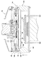
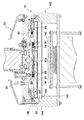
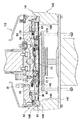
図3は図2に示す研磨部のトップリングユニット12を流路構成と共に示す概略図、図4は図3に示すトップリングユニット12のトップリング23を示す縦断面図である。図3及び図4に示すように、トップリング23は、自在継手部40を介してトップリングシャフト22に接続されており、トップリングシャフト22はトップリングヘッド21に固定されたトップリング用エアシリンダ111に連結されている。トップリング23は、トップリングシャフト22の下端に連結される略円盤状のトップリング本体42と、トップリング本体42の外周部に配置されたリテーナリング43とを備えている。トップリング本体42は金属やセラミックス等の強度及び剛性が高い材料から形成されている。また、リテーナリング43は、剛性の高い樹脂材又はセラミックス等から形成されている。
【0030】
トップリング用エアシリンダ111はレギュレータR1を介して圧力調整部120に接続されている。この圧力調整部120は、圧縮空気源から加圧空気等の加圧流体を供給することによって、あるいはポンプ等により真空引きすることによって圧力の調整を行うものである。この圧力調整部120によってトップリング用エアシリンダ111に供給される加圧空気の空気圧等をレギュレータR1を介して調整することができる。このトップリング用エアシリンダ111によってトップリングシャフト22は上下動し、トップリング23の全体を昇降させると共にトップリング本体42に取り付けられたリテーナリング43を所定の押圧力で研磨テーブル11に押圧できるようになっている。
【0031】
また、トップリングシャフト22はキー(図示せず)を介して回転筒112に連結されている。この回転筒112はその外周部にタイミングプーリ113を備えている。トップリングヘッド21にはトップリング用モータ114が固定されており、上記タイミングプーリ113は、タイミングベルト115を介してトップリング用モータ114に設けられたタイミングプーリ116に接続されている。従って、トップリング用モータ114を回転駆動することによってタイミングプーリ116、タイミングベルト115、及びタイミングプーリ113を介して回転筒112及びトップリングシャフト22が一体に回転し、トップリング23が回転する。なお、トップリングヘッド21は、フレーム(図示せず)に回転可能に支持された支軸20によって支持されている。
【0032】
図4に示すように、トップリング本体42は、円筒容器状のハウジング部42aと、ハウジング部42aの円筒部の内側に嵌合される環状の加圧シート支持部42bと、ハウジング部42aの上面の外周縁部に嵌合された環状のシール部42cとを備えている。トップリング本体42のハウジング部42aの下端にはリテーナリング43が固定されている。このリテーナリング43の下部は内方に突出している。
【0033】
トップリング本体42のハウジング部42aの中央部の上方には、上述したトップリングシャフト22が配設されており、トップリング本体42とトップリングシャフト22とは自在継手部40により連結されている。この自在継手部40は、トップリング本体42及びトップリングシャフト22とを互いに傾動可能とする球面軸受機構と、トップリングシャフト22の回転をトップリング本体42に伝達する回転伝達機構とを備えており、トップリングシャフト22からトップリング本体42に対して互いの傾動を許容しつつ押圧力及び回転力を伝達する。
【0034】
球面軸受機構は、トップリングシャフト22の下面の中央に形成された球面状凹部22aと、トップリング本体42の上面の中央部に形成された球面状凹部42dと、両凹部22a,42d間に介装されたセラミックスのような高硬度材料からなるベアリングボール52とから構成されている。図4に示すように、トップリング本体42のトップリングシャフト22の近傍には接続ボルト47が取り付けられており、この接続ボルト47とトップリングシャフト22に設けられたばね受け22bとの間にはコイルばね48が介装されている。このような構造によって、トップリング本体42はトップリングシャフト22に対して傾動可能に保持されるようになっている。
【0035】
一方、回転伝達機構は、トップリング本体42のトップリングシャフト22の近傍に固定された係合ピン49と、トップリングシャフト22に形成された係合孔22cとから構成される。トップリング本体42が傾いても係合ピン49は係合孔22c内を上下方向に移動可能であるため、係合ピン49は係合孔22cと接触点をずらして係合し、回転伝達機構がトップリングシャフト22の回転トルクをトップリング本体42に確実に伝達するようになっている。
【0036】
トップリング本体42及びリテーナリング43の内部に画成された空間内には、トップリング23によって保持される半導体ウェハWに当接する弾性パッド60と、環状のホルダーリング61と、トップリング本体42内部の収容空間内で上下動可能な概略円盤状のチャッキングプレート(上下動部材)62とが収容されている。弾性パッド60は、その外周部がホルダーリング61とホルダーリング61の下端に固定されたチャッキングプレート62との間に挟み込まれており、チャッキングプレート62の下面を覆っている。これにより弾性パッド60とチャッキングプレート62との間には圧力室70が形成されている。弾性パッド60は、エチレンプロピレンゴム(EPDM)、ポリウレタンゴム、シリコンゴム、ネオプレンゴム等の強度及び耐久性に優れたゴム材によって形成されている。
【0037】
チャッキングプレート62の中央部には開口62aが形成されている。この開口62aはチューブ、コネクタ等からなる流体路80に連通しており、流体路80上に配置されたレギュレータR2を介して圧力調整部120に接続されている。すなわち、弾性パッド60とチャッキングプレート62との間の圧力室70は、流体路80上に配置されたレギュレータR2を介して圧力調整部120に接続されている。また、弾性パッド60には、開口62aに対応する位置に大径(例えば直径12mm)の中央孔60aが形成されている。
【0038】
ホルダーリング61とトップリング本体42との間には弾性膜からなる加圧シート63が張設されている。この加圧シート63の一端は、トップリング本体42の下面に取り付けられた加圧シート支持部42bによって挟持され、他端はホルダーリング61の上端部61aとストッパ部61bとの間に挟持されている。トップリング本体42、チャッキングプレート62、ホルダーリング61、及び加圧シート63によってトップリング本体42の内部に圧力室71が形成されている。図4に示すように、圧力室71にはチューブ、コネクタ等からなる流体路81が連通されており、圧力室71は流体路81上に配置されたレギュレータR3を介して圧力調整部120に接続されている。なお、加圧シート63は、エチレンプロピレンゴム(EPDM)、ポリウレタンゴム、シリコンゴム、ネオプレンゴム等の強度及び耐久性に優れたゴム材もしくはファイバーを含み強化されたゴムや非常に薄いステンレス(例えば厚さ0.2mm)等によって形成されている。
【0039】
ここで、弾性パッド60の外周面とリテーナリング43との間には、わずかな間隙があるので、ホルダーリング61とチャッキングプレート62等の部材は、トップリング本体42及びリテーナリング43に対して上下方向に移動可能で、フローティングする構造となっている。ホルダーリング61のストッパ部61bには、その外周縁部から外方に突出する突起61cが複数箇所に設けられており、この突起61cがリテーナリング43の内方に突出している部分の上面に係合することにより、上記ホルダーリング61等の部材の下方への移動が所定の位置までに制限される。
【0040】
加圧シート63がゴムなどの弾性体である場合に、加圧シート63をリテーナリング43とトップリング本体42との間に挟み込んで固定した場合には、弾性体としての加圧シート63の弾性変形によってリテーナリング43の下面において好ましい平面が得られなくなってしまう。従って、これを防止するため、本実施形態では、別部材として加圧シート支持部42bを設けて、これをトップリング本体42のハウジング部42aと加圧シート支持部42bとの間に挟み込んで固定している。なお、リテーナリング43をトップリング本体42に対して上下動可能としたり、リテーナリング43をトップリング本体42とは独立に押圧可能な構造としたりすることもでき、このような場合には、必ずしも上述した加圧シート63の固定方法が用いられるとは限らない。
【0041】
上述したチャッキングプレート62と弾性パッド60との間の圧力室70及びチャッキングプレート62の上方の圧力室71には、それぞれの圧力室70,71に連通される流体路80,81を介して加圧空気等の加圧流体を供給する、あるいは大気圧や真空にすることができるようになっている。すなわち、図3に示すように、圧力室70,71の流体路80,81上に配置されたレギュレータR2,R3によってそれぞれの圧力室に供給される加圧流体の圧力を調整することができる。これにより各圧力室70,71の内部の圧力を各々独立に制御する又は大気圧や真空にすることができるようになっている。
【0042】
また、チャッキングプレート62には、下方に突出する内側吸着部64及び外側吸着部65が開口62aの外側に設けられている。内側吸着部64には、チューブ、コネクタ等からなる流体路82に連通する連通孔64aが形成されており、内側吸着部64はこの流体路82上に配置されたレギュレータR4を介して圧力調整部120に接続されている。同様に、外側吸着部65には、チューブ、コネクタ等からなる流体路83に連通する連通孔65aが形成されており、外側吸着部65はこの流体路83上に配置されたレギュレータR5を介して圧力調整部120に接続されている。圧力調整部120により吸着部64,65の連通孔64a,65aの開口端に負圧を形成し、吸着部64,65に半導体ウェハWを吸着することができる。なお、吸着部64,65の下端面には薄いゴムシートやバッキングフィルム等からなる弾性シートが貼着されており、吸着部64,65は半導体ウェハWを柔軟に吸着保持するようになっている。
【0043】
トップリング本体42のシール部42cの下面には環状の溝からなる洗浄液路91が形成されている。この洗浄液路91は流体路84に連通されている。また、シール部42cの洗浄液路91から延びハウジング部42a、加圧シート支持部42bを貫通する連通孔92が複数箇所形成されており、この連通孔92は弾性パッド60の外周面とリテーナリング43との間のわずかな間隙に連通されている。この洗浄液路91を介して洗浄液(純水)が間隙に供給されるようになっている。
【0044】
次に、このような構成のポリッシング装置の動作を説明する。まず、第1搬送ロボット4aで半導体ウェハWをカセット2a又は2bから取り出し、反転機5又は6で反転させた後、第2搬送ロボット4bでプッシャ14上に搬送して載置する。この状態で、トップリングユニット12のトップリングヘッド21を揺動させてトップリング23をプッシャ14の上方に移動させる。
【0045】
図5は、このときの状態を示す縦断面図である。図5に示すように、プッシャ14は、エアシリンダ等により上下動可能なガイドステージ141と、この外周部に設けられたウェハガイド142と、ガイドステージ141の上方に配置され、ガイドステージ141とは独立に上下動可能なプッシュステージ143とを備えている。ウェハガイド142は、上段部144と下段部145とを有する2段の階段構造となっている。ウェハガイド142の上段部144はトップリング23のリテーナリング43の下面とのアクセス部であり、下段部145は半導体ウェハWの求芯用及び保持用である。上段部144の上方にはリテーナリング43を導くためのテーパ146が形成されており、下段部145の上方には半導体ウェハWを導くためのテーパ147が形成されている。半導体ウェハWは、ウェハガイド142のテーパ147によって求芯された状態で、ウェハガイド142の下段部145に載置される。
【0046】
ここで、図5に示す状態においては、トップリング23内の圧力室71を流路81を介して圧力調整部120に接続し、圧力室71を負圧にしておく。これにより、チャッキングプレート62は、図5に示すように、リテーナリング43に対して上方に位置することとなる。このようにすることで、後述するように半導体ウェハWの吸着を確実に行うことが可能となる。
【0047】
次に、図6に示すように、プッシャ14のガイドステージ141を上昇させ、ウェハガイド142のテーパ146によってリテーナリング43をウェハガイド142の上段部144に導く。ウェハガイド142の上段部144がリテーナリング43の下面と接触することでガイドステージ141の上昇が終了する。
【0048】
この状態で、図7に示すように、プッシャ14のプッシュステージ143が上昇して、ウェハガイド142の下段部145に載置された半導体ウェハWのパターン面を保持して、半導体ウェハWをトップリング23の弾性パッド60に当接させる。そして、吸着部64,65の連通孔64a,65aを流体路82,83を介して圧力調整部120に接続し、この連通孔64a,65aの吸引作用により吸着部64,65の下端面に半導体ウェハWを真空吸着する。
【0049】
この半導体ウェハWの受け渡しの際に、チャッキングプレート62がリテーナリング43よりも下方に突出していると、半導体ウェハWがずれた位置で吸着された場合に、その後のチャッキングプレート62の上昇によって半導体ウェハWがリテーナリング43に引っ掛かりウェハの脱落や破損の原因となるおそれがある。本実施形態では、上述したように、トップリング23内の圧力室71を負圧にして予めチャッキングプレート62をリテーナリング43に対して上方に位置させているので、半導体ウェハWはその外周部がリテーナリング43にガイドされながら受け渡しされることとなる。従って、半導体ウェハWがチャッキングプレート62の上昇によってリテーナリング43に引っ掛かることがなくなり、ウェハの脱落や破損を防止することができる。
【0050】
半導体ウェハWの吸着が完了すると、プッシャ14を下降させ、トップリングヘッド21を水平に揺動させて半導体ウェハWを吸着させた状態で研磨面10の上方に移動させる。なお、半導体ウェハWの外周縁はリテーナリング43によって保持され、半導体ウェハWがトップリング23から飛び出さないようになっている。そして、トップリング23を回転させながら下降させ、回転している研磨テーブル11上の研磨面10に向けて半導体ウェハWを押圧する。すなわち、研磨時には、吸着部64,65による半導体ウェハWの吸着を解除し、トップリング23の下面に半導体ウェハWを保持させると共に、トップリングシャフト22に連結されたトップリング用エアシリンダ111を作動させてトップリング23の下端に固定されたリテーナリング43を所定の押圧力で研磨テーブル11の研磨面10に押圧する。この状態で、圧力室70に所定圧力の加圧流体を供給し、半導体ウェハWを研磨テーブル11の研磨面に押圧する。このとき、研磨液供給ノズル15から研磨液を供給しながら半導体ウェハWの研磨される面(下面)と研磨面10との間に研磨液が存在した状態で半導体ウェハWの研磨が行われる。図4はこの研磨時の状態を示している。
【0051】
上述のようにして、トップリング用エアシリンダ111によってリテーナリング43が研磨面10に押圧される力と、圧力室70に供給する加圧空気によって半導体ウェハWが研磨面10に押圧される力とを適宜調整して半導体ウェハWの研磨が行われる。なお、圧力室70に加圧流体を供給すると、チャッキングプレート62は上方向の力を受けるので、本実施形態では、圧力室71に流体路81を介して圧力流体を供給し、圧力室70からの力によりチャッキングプレート62が上方に持ち上げられるのを防止している。
【0052】
研磨終了後は、図8に示すように、圧力室70への加圧流体の供給を止め、大気圧に開放することにより、チャッキングプレート62を下降させ、吸着部64,65の下端面を半導体ウェハWに当接させる。また、圧力室71内の圧力を大気圧に開放するか、もしくは負圧にする。これは、圧力室71の圧力を高いままにしておくと、半導体ウェハWの吸着部64,65に当接している部分のみが、研磨面に強く押圧されることになってしまうためである。そして、半導体ウェハWを吸着部64,65の下端面に再び真空吸着させる。このように、研磨終了時にチャッキングプレート62を下降させることで、半導体ウェハWを吸着部64,65に確実に吸着することが可能となる。
【0053】
そして、半導体ウェハWを吸着させた状態でトップリング23をオーバーハング位置まで移動させ、図9に示すように、圧力室71を流路81を介して圧力調整部120に接続してトップリング23内の圧力室71を負圧にし、チャッキングプレート62をリテーナリング43に対して上方に位置させる。この状態で、トップリング23を上昇させ、トップリングヘッド21を水平に揺動させてトップリング23を図10に示すように再びプッシャ14の上方まで移動させる。
【0054】
次に、図11に示すように、プッシャ14のガイドステージ141を上昇させ、ウェハガイド142のテーパ146によってリテーナリング43をウェハガイド142の上段部144に導く。そして、ウェハガイド142の上段部144がリテーナリング43の下面と接触することでガイドステージ141の上昇が終了する。
【0055】
この状態で、図12に示すように、チャッキングプレート62の中央部の開口62a及び吸着部64,65をそれぞれ流体路80,82,83を介して圧力調整部120に接続し、開口62a及び吸着部64,65から加圧流体(例えば、圧縮空気もしくは窒素と純水を混合したもの)を例えば0.2MPaの圧力で下方に噴射する(ウォータスパウト)。この流体の噴射により、弾性パッド60の下面から半導体ウェハWが離脱して、ウェハガイド142のテーパ147によって求芯された状態で、ウェハガイド142の下段部145に保持されることとなる。
【0056】
このように、本実施形態では、チャッキングプレート62の中央部に形成された大径の開口62a及び吸着部64,65から加圧流体を噴射するため、弾性パッド60と半導体ウェハWとが密着している部分にも加圧流体が送り込まれるので、より確実に半導体ウェハWを離脱することができる。
【0057】
このようにして、研磨後の半導体ウェハWがトップリング23からプッシャ14に渡され、必要に応じて純水又は洗浄液により半導体ウェハW及びトップリング23の洗浄を行う。その後、トップリング23はプッシャ14から新たな半導体ウェハWを受け取って研磨テーブル10上に移動し、新たな研磨を行う。
【0058】
所定の研磨量だけ半導体ウェハWを研磨した時点で研磨処理が終了するが、この研磨作業の終了時点では、研磨によって研磨面10の特性が変化し、次に行う研磨の研磨性能が低下しているので、ドレッシングユニット13により研磨面10のドレッシングを行う。ドレッシングは、ドレッサ33及び研磨テーブル11をそれぞれ独立に自転させつつ、ドレッシング部材34を所定の押圧力で研磨面10に当接させる。このとき、ドレッシング部材34が研磨面10に接触するのと同時又は接触する前に、水供給ノズル16から研磨面10の上面に水を供給し、研磨面10に残留している使用済みの研磨液を洗い流す。ドレッシング終了後のドレッサ33は、ドレッシングヘッド31の駆動により待機位置に戻され、この待機位置に設置されたドレッサ洗浄装置18(図1参照)によって洗浄される。
【0059】
プッシャ14上に載置された研磨後の半導体ウェハWは、第2搬送ロボット4bにより、例えばロールスポンジによる両面洗浄機能を有する洗浄機7a又は7bに搬送し、この洗浄機7a又は7bで基板Wの両面を洗浄した後、第2搬送ロボット4bでこれを反転機5又は6に搬送して反転させる。その後、第1搬送ロボット4aで反転機5又は6上の半導体ウェハWを取り出し、これを、例えば上面洗浄のペンスポンジとスピンドライ機能を具備する第2の洗浄機8a又は8bに搬送して洗浄・乾燥させ、第1搬送ロボット4aでカセット2a,2bに戻す。
【0060】
次に、本発明に係るポリッシング方法の第2の実施形態について図13乃至図22を参照して詳細に説明する。なお、上述の第1の実施形態における部材又は要素と同一の作用又は機能を有する部材又は要素には同一の符号を付し、特に説明しない部分については第1の実施形態と同様である。また、トップリング以外の構成については基本的に上述の第1の実施形態と同様である。
【0061】
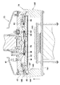
図13は、本発明の第2の実施形態におけるトップリングを示す縦断面図である。本実施形態においては、トップリング本体42及びトップリング本体42に一体に固定されたリテーナリング43の内部に画成された空間内には、トップリング123によって保持される半導体ウェハWの外周部に当接するアウターメンブレン160が収容されており、第1の実施形態における弾性パッドは設けられていない。
【0062】
アウターメンブレン160は、その外周部がホルダーリング61とホルダーリング61の下端に固定されたチャッキングプレート62との間に挟み込まれており、チャッキングプレート62の外縁近傍の下面を覆っている。このアウターメンブレン160の下端面は、ポリッシング対象物である半導体ウェハWの上面に接する。アウターメンブレン160は、エチレンプロピレンゴム(EPDM)、ポリウレタンゴム、シリコンゴム等の強度及び耐久性に優れたゴム材によって形成されている。なお、半導体ウェハWの外縁にはノッチやオリエンテーションフラットと呼ばれる、半導体ウェハの向きを認識(特定)するための切り欠きが設けられているが、このようなノッチやオリエンテーションフラットよりもチャッキングプレート62の内周側にまでアウターメンブレン160が延出していることが好ましい。
【0063】
また、チャッキングプレート62と半導体ウェハWとの間に形成される空間の内部には、半導体ウェハWに当接する当接部材としてのリングチューブ170が設けられている。本実施形態においては、図13に示すように、リングチューブ170はチャッキングプレート62の中央部の開口62aを取り囲むように配置されている。また、本実施形態においては、リングチューブ170の外側に外側吸着部65のみが設けられており、内側吸着部は設けられていない。
【0064】
リングチューブ170は、半導体ウェハWの上面に当接する弾性膜171と、弾性膜171を着脱可能に保持するリングチューブホルダー172とから構成されており、これらの弾性膜171とリングチューブホルダー172によってリングチューブ170の内部に圧力室72が形成されている。また、チャッキングプレート62と半導体ウェハWとの間に形成される空間は、上記リングチューブ170によって複数の空間に区画されており、リングチューブ170の内側、すなわちチャッキングプレート62の中央部の開口62aの周囲には圧力室73が、リングチューブ170の外側、すなわち吸着部65の周囲には圧力室74がそれぞれ形成されている。なお、リングチューブ170の弾性膜171は、エチレンプロピレンゴム(EPDM)、ポリウレタンゴム、シリコンゴム等の強度及び耐久性に優れたゴム材によって形成されている。
【0065】
リングチューブ170の弾性膜171には、半導体ウェハWが当接する面に孔171aが形成されている。この孔171aは、例えば、図14(a)及び図14(b)に示すように、複数の楕円又は円を組み合わせた形状としてもよく、図14(c)に示すように楕円に三角形状の切り込みを形成したものでもよく、あるいは図14(d)に示すように大きな楕円形状であってもよい。また、図14(e)に示すように正方形やひし形であってもよく、図14(f)及び図14(g)に示すように単なるスリットであってもよい。
【0066】
リングチューブ170内の圧力室72には、チューブ、コネクタ等からなる流体路85が連通されており、圧力室72はこの流体路85上に配置されたレギュレータを介して圧力調整部120(図3参照)に接続されている。また、圧力室73はチューブ、コネクタ等からなる流体路86に連通しており、圧力室73はこの流体路86上に配置されたレギュレータを介して圧力調整部120に接続されている。
【0067】
上述したチャッキングプレート62の上方の圧力室71及び上記圧力室72,73,74には、各圧力室に連通される流体路81,85,86,83を介して加圧空気等の加圧流体を供給する、あるいは大気圧や真空にすることができるようになっている。すなわち、圧力室71〜74の流体路81,85,86,83上に配置されたレギュレータによってそれぞれの圧力室に供給される加圧流体の圧力を調整することができる。これにより各圧力室71〜74の内部の圧力を各々独立に制御する又は大気圧や真空にすることができるようになっている。このように、レギュレータによって各圧力室71〜74の内部の圧力を独立に可変とすることにより、半導体ウェハWを研磨パッド10に押圧する押圧力を半導体ウェハWの部分ごとに調整することができる。
【0068】
この場合において、各圧力室72〜74に供給される加圧流体や大気圧の温度をそれぞれ制御することとしてもよい。このようにすれば、半導体ウェハ等の研磨対象物の被研磨面の裏側から研磨対象物の温度を直接制御することができる。特に、各圧力室の温度を独立に制御することとすれば、CMPにおける化学的研磨の化学反応速度を制御することが可能となる。
【0069】
次に、本実施形態におけるポリッシング装置の動作を説明する。まず、第1搬送ロボット4aで半導体ウェハWをカセット2a又は2bから取り出し、反転機5又は6で反転させた後、第2搬送ロボット4bでプッシャ14上に搬送して載置する。この状態で、トップリングユニット12のトップリングヘッド21を揺動させてトップリング123をプッシャ14の上方に移動させる。
【0070】
図15は、このときの状態を示す縦断面図である。図15に示す状態においては、トップリング123内の圧力室71を流路81を介して圧力調整部120に接続し、圧力室71を負圧にしておく。これにより、チャッキングプレート62は、図15に示すように、リテーナリング43に対して上方に位置することとなる。第1の実施形態と同様に、このようにすることで半導体ウェハWの吸着を確実に行うことが可能となる。
【0071】
次に、図16に示すように、プッシャ14のガイドステージ141を上昇させ、ウェハガイド142のテーパ146によってリテーナリング43をウェハガイド142の上段部144に導く。ウェハガイド142の上段部144がリテーナリング43の下面と接触することでガイドステージ141の上昇が終了する。
【0072】
この状態で、図17に示すように、プッシャ14のプッシュステージ143が上昇して、ウェハガイド142の下段部145に載置された半導体ウェハWのパターン面を保持して、半導体ウェハWをトップリング123のアウターメンブレン160及びリングチューブ170に当接させる。そして、リングチューブ170内の圧力室72、及び圧力室73,74に連通した流体路85,86,83を圧力調整部120に接続し、流体路85,86,83を負圧にして半導体ウェハWを真空吸着する。例えば、流体路83の圧力を−80kPa、流体路85,86の圧力を−20kPaとして半導体ウェハWを真空吸着する。
【0073】
このとき、上述したように、トップリング123内の圧力室71を負圧にして予めチャッキングプレート62をリテーナリング43に対して上方に位置させているので、半導体ウェハWはその外周部がリテーナリング43にガイドされながら受け渡しされることとなる。従って、半導体ウェハWがチャッキングプレート62の上昇によってリテーナリング43に引っ掛かることがなくなり、ウェハの脱落や破損を防止することができる。
【0074】
半導体ウェハWの吸着が完了すると、プッシャ14を下降させ、トップリングヘッド21を水平に揺動させて半導体ウェハWを吸着させた状態で研磨面10の上方に移動させる。なお、半導体ウェハWの外周縁はリテーナリング43によって保持され、半導体ウェハWがトップリング123から飛び出さないようになっている。そして、トップリング123を回転させながら下降させ、回転している研磨テーブル11上の研磨面10に向けて半導体ウェハWを押圧する。すなわち、研磨時には、半導体ウェハWの吸着を解除し、トップリング123の下面に半導体ウェハWを保持させると共に、トップリングシャフト22に連結されたトップリング用エアシリンダ111を作動させてトップリング123の下端に固定されたリテーナリング43を所定の押圧力で研磨テーブル11の研磨面10に押圧する。この状態で、圧力室72,73,74にそれぞれ所定圧力の加圧流体を供給し、半導体ウェハWを研磨テーブル11の研磨面に押圧する。このとき、研磨液供給ノズル15から研磨液を供給しながら半導体ウェハWの研磨される面(下面)と研磨面10との間に研磨液が存在した状態で半導体ウェハWの研磨が行われる。図13はこの研磨時の状態を示している。
【0075】
上述のようにして、トップリング用エアシリンダ111によってリテーナリング43が研磨面10に押圧される力と、圧力室72〜74に供給する加圧空気によって半導体ウェハWが研磨面10に押圧される力とを適宜調整して半導体ウェハWの研磨が行われる。なお、圧力室72〜74に加圧流体を供給すると、チャッキングプレート62は上方向の力を受けるので、本実施形態では、圧力室71に流体路81を介して圧力流体を供給し、圧力室72からの力によりチャッキングプレート62が上方に持ち上げられるのを防止している。
【0076】
研磨終了後は、図18に示すように、圧力室72〜74への加圧流体の供給を止め、大気圧に開放することにより、チャッキングプレート62を下降させ、吸着部65の下端面を半導体ウェハWに当接させる。また、圧力室71内の圧力を大気圧に開放するか、もしくは負圧にする。これは、圧力室71の圧力を高いままにしておくと、半導体ウェハWの吸着部65に当接している部分のみが、研磨面に強く押圧されることになってしまうためである。そして、半導体ウェハWを吸着部65の下端面に再び真空吸着させる。研磨終了時には、半導体ウェハWとチャッキングプレート62が離れている場合があり、そのまま吸着部65により半導体ウェハWを吸着させようとしても吸着できない場合がある。そこで、本実施形態では、上述したように、研磨終了時にチャッキングプレート62を下降させることで、半導体ウェハWを吸着部65に確実に吸着させている。
【0077】
そして、半導体ウェハWを吸着させた状態でトップリング123をオーバーハング位置まで移動させ、図19に示すように、圧力室71を流路81を介して圧力調整部120に接続してトップリング123内の圧力室71を負圧にし、チャッキングプレート62をリテーナリング43に対して上方に位置させる。この状態で、トップリング123を上昇させ、トップリングヘッド21を水平に揺動させてトップリング123を図20に示すように再びプッシャ14の上方まで移動させる。このとき、リングチューブ170内の圧力室72に加圧流体を供給して加圧しておくことが好ましく、このようにすることで半導体ウェハWがアウターメンブレン160及びリングチューブ170から離脱しやすくなる。
【0078】
次に、図21に示すように、プッシャ14のガイドステージ141を上昇させ、ウェハガイド142のテーパ146によってリテーナリング43をウェハガイド142の上段部144に導く。ウェハガイド142の上段部144がリテーナリング43の下面と接触することでガイドステージ141の上昇が終了する。
【0079】
この状態で、図22に示すように、チャッキングプレート62の中央部の開口62a及び吸着部65をそれぞれ流体路86,83を介して圧力調整部120に接続し、開口62a及び吸着部65から加圧流体(例えば、圧縮空気もしくは窒素と純水を混合したもの)を下方に噴射する(ウォータスパウト)。また、リングチューブ170内の圧力室72を圧力調整部120に接続し、リングチューブ170の弾性膜171に形成された孔171a(図13参照)から加圧流体(例えば、圧縮空気もしくは窒素と純水を混合したもの)を下方に噴射する(ウォータスパウト)。これらの流体の噴射により、トップリング123から半導体ウェハWが離脱して、ウェハガイド142のテーパ147によって求芯された状態で、ウェハガイド142の下段部145に保持されることとなる。例えば、開口62aからは0.03MPa、吸着部65からは0.2MPa、リングチューブ170の孔171aからは0.05MPaの圧力でそれぞれ流体を噴射する。この場合において、リングチューブ170の弾性膜171と半導体ウェハWとの密着性を解消しやすくするために、まず最初にリングチューブ170の孔171aから流体を噴射した後、開口62a及び吸着部65から流体を噴射することが好ましい。
【0080】
このように、本実施形態では、チャッキングプレート62の中央部に形成された大径の開口62a及び吸着部65、更にリングチューブ170の弾性膜171に形成された孔171aからそれぞれ加圧流体を噴射するため、アウターメンブレン160及びリングチューブ170の弾性膜171と半導体ウェハWとが密着している部分にも加圧流体が送り込まれるので、より確実に半導体ウェハWを離脱することができる。また、リングチューブ170の弾性膜171に形成する孔171aの形状を図14(c)又は図14(d)に示す形状とすれば、半導体ウェハWの離脱時の音もなく、よりスムーズに半導体ウェハWを離脱させることができる。
【0081】
上述の実施形態では、流体路80〜86をそれぞれ別個に設けたが、これらの流体路を統合したり、各圧力室同士を連通させたりするなど、半導体ウェハWに加えるべき押圧力の大きさや加える位置により自由に改変することが可能である。また、上述した実施形態においては、リングチューブ170が直接半導体ウェハWに接触する例を説明したが、これに限られるものではなく、例えば、リングチューブ170と半導体ウェハWとの間に弾性パッドを介在させ、リングチューブ170が間接的に半導体ウェハWに接触することとしてもよい。
【0082】
また、上述した実施形態においては、研磨パッドにより研磨面が形成されることとしたが、これに限られるものではない。例えば、固定砥粒により研磨面を形成してもよい。固定砥粒は、砥粒をバインダ中に固定し板状に形成されたものである。固定砥粒を用いた研磨においては、固定砥粒から自生した砥粒により研磨が進行する。固定砥粒は砥粒とバインダと気孔により構成されており、例えば砥粒には平均粒径0.5μm以下の酸化セリウム(CeO2)、バインダにはエポキシ樹脂を用いる。このような固定砥粒は硬質の研磨面を構成する。また、固定砥粒には、上述した板状のものの他に、薄い固定砥粒層の下に弾性を有する研磨パッドを貼付して二層構造とした固定砥粒パッドも含まれる。その他の硬質の研磨面としては、上述したIC−1000がある。
【0083】
これまで本発明の一実施形態について説明したが、本発明は上述の実施形態に限定されず、その技術的思想の範囲内において種々異なる形態にて実施されてよいことは言うまでもない。
【0085】
【発明の効果】
上述したように、本発明によれば、研磨終了時に上下動部材を下方に移動させて研磨対象物を吸着部に当接させてから研磨対象物を吸着保持するので、研磨対象物を確実に吸着させることが可能となる。
【図面の簡単な説明】
【図1】本発明の第1の実施形態におけるポリッシング装置を模式的に示す平面図である。
【図2】図1に示すポリッシング装置の研磨部の要部を示す縦断面図である。
【図3】図2に示す研磨部のトップリングユニットを流路構成と共に示す概略図である。
【図4】図3に示すトップリングユニットのトップリングを示す縦断面図である。
【図5】図4に示すトップリングとプッシャとの関係を示す縦断面図である。
【図6】図4に示すトップリングとプッシャとの関係を示す縦断面図である。
【図7】図4に示すトップリングとプッシャとの関係を示す縦断面図である。
【図8】図4に示すトップリングの研磨終了後の状態を示す縦断面図である。
【図9】図4に示すトップリングの研磨終了後の状態を示す縦断面図である。
【図10】図4に示すトップリングとプッシャとの関係を示す縦断面図である。
【図11】図4に示すトップリングとプッシャとの関係を示す縦断面図である。
【図12】図4に示すトップリングとプッシャとの関係を示す縦断面図である。
【図13】本発明の第2の実施形態におけるトップリングを示す縦断面図である。
【図14】 図14(a)乃至図14(g)は図13に示すトップリングのリングチューブの弾性膜に形成される孔の形状を示す概略図である。
【図15】図13に示すトップリングとプッシャとの関係を示す縦断面図である。
【図16】図13に示すトップリングとプッシャとの関係を示す縦断面図である。
【図17】図13に示すトップリングとプッシャとの関係を示す縦断面図である。
【図18】図13に示すトップリングの研磨終了後の状態を示す縦断面図である。
【図19】図13に示すトップリングの研磨終了後の状態を示す縦断面図である。
【図20】図13に示すトップリングとプッシャとの関係を示す縦断面図である。
【図21】図13に示すトップリングとプッシャとの関係を示す縦断面図である。
【図22】図13に示すトップリングとプッシャとの関係を示す縦断面図である。
【符号の説明】
1a,1b 研磨部
2a,2b 半導体ウェハ収納用カセット
4a,4b 搬送ロボット
5, 6 反転機
7a,7b,8a,8b 洗浄機
10 研磨パッド
11 研磨テーブル
11a テーブル軸
12 トップリングユニット
13 ドレッシングユニット
14 プッシャ
15 研磨液供給ノズル
16 水供給ノズル
17 枠体
17a 樋
18 ドレッサ洗浄装置
20,30 支軸
21 トップリングヘッド
22 トップリングシャフト
22a 球面状凹部
22b ばね受け
22c 係合孔
23,123 トップリング
31 ドレッサヘッド
32 ドレッサーシャフト
33 ドレッサ
34 ドレッシング部材
40 自在継手部
42 トップリング本体
42a ハウジング部
42b 加圧シート支持部
42c シール部
42d 球面上凹部
43 リテーナリング
47 接続ボルト
48 コイルばね
49 係合ピン
52 ベアリングボール
60 弾性パッド
60a 中央孔
61 ホルダーリング
61a 上端部
61b ストッパ部
61c 突起
62 チャッキングプレート
62a 開口
63 加圧シート
70〜74 圧力室
80〜86 流体路
64,65 吸着部
64a,65a 連通孔
91 洗浄液路
92 貫通孔
111 トップリング用エアシリンダ
112 回転筒
113,116 タイミングプーリ
114 トップリング用モータ
115 タイミングベルト
120 圧力調整部
141 ガイドステージ
142 ウェハガイド
143 プッシュステージ
144 上段部
145 下段部
146,147 テーパ
160 アウターメンブレン
170 リングチューブ
171 弾性膜
172 リングチューブホルダー
R1,R2,R3,R4,R5 レギュレータ
W 半導体ウェハ[0001]
BACKGROUND OF THE INVENTION
The present invention relates to a polishing method, and more particularly to a polishing method for polishing an object to be polished such as a semiconductor wafer having a thin film formed on a surface in a flat and mirror-like manner.
[0002]
[Prior art]
In recent years, semiconductor devices have become increasingly finer and the element structure has become more complex, and as the number of layers of logic-based multilayer wiring has increased, the unevenness of the surface of the semiconductor device has increased and the level difference has a tendency to increase. This is because, in the manufacture of semiconductor devices, the process of forming a thin film, micropatterning for patterning and opening and then forming the next thin film is repeated many times.
[0003]
If the irregularities on the surface of the semiconductor device increase, the film thickness at the stepped part will become thinner during thin film formation, open due to disconnection of the wiring, short circuit due to insulation failure between wiring layers, etc. There is a tendency to decrease. In addition, even if the device normally operates normally at the beginning, a problem of reliability occurs for a long time use. Furthermore, if the irradiation surface has irregularities at the time of exposure in the lithography process, the lens focus of the exposure system becomes partially unfocused. Therefore, if the irregularities on the surface of the semiconductor device increase, it becomes difficult to form a fine pattern itself.
[0004]
Accordingly, in the semiconductor device manufacturing process, a planarization technique for the surface of the semiconductor device is becoming increasingly important. Among the planarization techniques, the most important technique is chemical mechanical polishing (CMP). This chemical mechanical polishing is performed by using a polishing apparatus with silica (SiO 2).2The polishing liquid containing abrasive grains such as) is supplied onto a polishing surface such as a polishing pad, and a substrate such as a semiconductor wafer is brought into sliding contact with the polishing surface for polishing.
[0005]
This type of polishing apparatus includes a polishing table having a polishing surface made of a polishing pad, and a top ring or carrier head for holding a semiconductor wafer. When polishing a semiconductor wafer using such a polishing apparatus, the semiconductor wafer is pressed against the polishing table with a predetermined pressure while the semiconductor wafer is held by the top ring. At this time, by moving the polishing table and the top ring relative to each other, the semiconductor wafer comes into sliding contact with the polishing surface, and the surface of the semiconductor wafer is polished to a flat and mirror surface.
[0006]
In such a polishing apparatus, when the relative pressing force between the semiconductor wafer being polished and the polishing surface of the polishing pad is not uniform over the entire surface of the semiconductor wafer, it is applied to each part of the semiconductor wafer. Depending on the pressing force, insufficient polishing or overpolishing occurs. Therefore, the holding surface of the top ring semiconductor wafer is formed of an elastic film made of an elastic material such as rubber, and fluid pressure such as air pressure is applied to the back surface of the elastic film so that the pressing force applied to the semiconductor wafer is uniform over the entire surface. It is also done.
[0007]
In addition, since the polishing pad has elasticity, the pressing force applied to the outer peripheral edge of the semiconductor wafer being polished becomes non-uniform, so that only the outer peripheral edge of the semiconductor wafer is polished, so-called “edge fringing” is caused. May end up. In order to prevent such edge fringing, a top having a structure in which the outer peripheral edge of the semiconductor wafer is held by a guide ring or a retainer ring and the polishing surface located on the outer peripheral edge side of the semiconductor wafer is pressed by the guide ring or the retainer ring. A ring is also used.
[0008]
[Problems to be solved by the invention]
When polishing using such a top ring, it is necessary to attract and hold the conveyed semiconductor wafer on the top ring. Further, after the polishing is completed, it is necessary to remove the semiconductor wafer from the top ring at the transfer position after adsorbing the semiconductor wafer again to the top ring. However, in the top ring using the elastic film described above, the semiconductor wafer may not be successfully adsorbed and detached due to the presence of the elastic film.
[0009]
The present invention has been made in view of such problems of the prior art, and even when polishing is performed while holding an object to be polished via an elastic film, the object to be polished is reliably adsorbed and removed. An object of the present invention is to provide a polishing method capable of performing
[0014]
[Means for Solving the Problems]
In order to solve such problems in the prior art,Main departureTomorrowIn a polishing method for holding a polishing object by a top ring and pressing the polishing object against a polishing surface for polishing, a top ring main body and a vertically moving member attached to the lower surface of the top ring main body so as to freely move up and down. Forming a first pressure chamber therebetween, forming a second pressure chamber between the elastic film having a hole in the contact surface in contact with the polishing object held by the top ring and the vertical movement member; A pressurized fluid is supplied into the first and second pressure chambers to polish the object to be polished against the polishing surface by the fluid pressure of the fluid, and after the polishing is finished, the pressure in the first pressure chamber is reduced. Opening to atmospheric pressure, setting the second pressure chamber to a negative pressure, moving the vertical movement member downward, and bringing the object to be polished into contact with an adsorbing portion that protrudes downward from the vertical movement member The top surface of the object to be polished by the suction portion. A polishing method characterized by sucking and holding the grayed.
[0015]
At the end of polishing, there is a case where the object to be polished and the vertically moving member are separated from each other. According to the present invention, when the polishing is completed, the vertically moving member is moved downward to bring the polishing object into contact with the suction portion, and then the polishing object is sucked and held, so that the polishing object can be reliably sucked. It becomes.
[0018]
DETAILED DESCRIPTION OF THE INVENTION
Hereinafter, a first embodiment of a polishing method according to the present invention will be described in detail with reference to FIGS. FIG. 1 is a plan view schematically showing a polishing apparatus according to the first embodiment of the present invention. As shown in FIG. 1, in the polishing apparatus, a pair of
[0019]
The two
[0020]
The
[0021]
The reversing
[0022]
The type of each cleaning
[0023]
Next, details of the above-described polishing unit will be described. FIG. 2 is a longitudinal sectional view showing a main part of the polishing
[0024]
As shown in FIG. 2, the polishing
[0025]
There are various types of polishing pads available on the market, such as SUBA800, IC-1000, IC-1000 / SUBA400 (double-layer cloth) manufactured by Rodel, Surfin xxx-5 manufactured by Fujimi Incorporated, Surfin 000 etc. SUBA800, Surfin xxx-5, and Surfin 000 are non-woven fabrics in which fibers are hardened with urethane resin, and IC-1000 is a hard foamed polyurethane (single layer). The polyurethane foam is porous (porous) and has a large number of fine dents or pores on its surface.
[0026]
A polishing
[0027]
The
[0028]
The
[0029]
3 is a schematic view showing the
[0030]
The top
[0031]
The
[0032]
As shown in FIG. 4, the top ring
[0033]
The above-described
[0034]
The spherical bearing mechanism includes a
[0035]
On the other hand, the rotation transmission mechanism includes an
[0036]
In a space defined inside the
[0037]
An
[0038]
A
[0039]
Here, since there is a slight gap between the outer peripheral surface of the
[0040]
When the
[0041]
The
[0042]
Further, the chucking
[0043]
A cleaning
[0044]
Next, the operation of the polishing apparatus having such a configuration will be described. First, the semiconductor wafer W is taken out from the
[0045]
FIG. 5 is a longitudinal sectional view showing the state at this time. As shown in FIG. 5, the
[0046]
Here, in the state shown in FIG. 5, the
[0047]
Next, as shown in FIG. 6, the
[0048]
In this state, as shown in FIG. 7, the
[0049]
If the chucking
[0050]
When the suction of the semiconductor wafer W is completed, the
[0051]
As described above, the force by which the
[0052]
After completion of the polishing, as shown in FIG. 8, the supply of the pressurized fluid to the
[0053]
Then, the
[0054]
Next, as shown in FIG. 11, the
[0055]
In this state, as shown in FIG. 12, the
[0056]
As described above, in this embodiment, since the pressurized fluid is ejected from the large-
[0057]
In this way, the polished semiconductor wafer W is transferred from the
[0058]
The polishing process ends when the semiconductor wafer W is polished by a predetermined polishing amount. At the end of this polishing operation, the characteristics of the polishing
[0059]
The polished semiconductor wafer W placed on the
[0060]
Next, a second embodiment of the polishing method according to the present invention will be described in detail with reference to FIGS. In addition, the same code | symbol is attached | subjected to the member or element which has the same effect | action or function as the member or element in the above-mentioned 1st Embodiment, and the part which is not demonstrated in particular is the same as that of 1st Embodiment. The configuration other than the top ring is basically the same as that of the first embodiment described above.
[0061]
FIG. 13 is a longitudinal sectional view showing a top ring in the second embodiment of the present invention. In the present embodiment, in the space defined inside the top ring
[0062]
The
[0063]
A
[0064]
The
[0065]
In the
[0066]
The
[0067]
The
[0068]
In this case, it is good also as controlling the temperature of the pressurized fluid and atmospheric pressure which are supplied to each pressure chamber 72-74, respectively. In this way, the temperature of the polishing object can be directly controlled from the back side of the surface to be polished of the polishing object such as a semiconductor wafer. In particular, if the temperature of each pressure chamber is controlled independently, the chemical reaction rate of chemical polishing in CMP can be controlled.
[0069]
Next, the operation of the polishing apparatus in this embodiment will be described. First, the semiconductor wafer W is taken out from the
[0070]
FIG. 15 is a longitudinal sectional view showing the state at this time. In the state shown in FIG. 15, the
[0071]
Next, as shown in FIG. 16, the
[0072]
In this state, as shown in FIG. 17, the
[0073]
At this time, as described above, since the
[0074]
When the suction of the semiconductor wafer W is completed, the
[0075]
As described above, the semiconductor wafer W is pressed against the polishing
[0076]
After the polishing is finished, as shown in FIG. 18, the supply of the pressurized fluid to the
[0077]
Then, the
[0078]
Next, as shown in FIG. 21, the
[0079]
In this state, as shown in FIG. 22, the
[0080]
As described above, in this embodiment, pressurized fluid is respectively supplied from the large-
[0081]
In the above-described embodiment, the
[0082]
In the embodiment described above, the polishing surface is formed by the polishing pad. However, the present invention is not limited to this. For example, the polishing surface may be formed by fixed abrasive grains. The fixed abrasive is a plate formed by fixing the abrasive in a binder. In polishing using fixed abrasive grains, polishing proceeds by abrasive grains spontaneously generated from the fixed abrasive grains. The fixed abrasive is composed of abrasive grains, a binder, and pores. For example, the abrasive grains include cerium oxide (CeO) having an average particle diameter of 0.5 μm or less.2) An epoxy resin is used for the binder. Such fixed abrasive grains constitute a hard polishing surface. The fixed abrasive also includes a fixed abrasive pad having a two-layer structure in which a polishing pad having elasticity is stuck under a thin fixed abrasive layer in addition to the plate-like one described above. Other hard polishing surfaces include the IC-1000 described above.
[0083]
Although one embodiment of the present invention has been described so far, it is needless to say that the present invention is not limited to the above-described embodiment, and may be implemented in various forms within the scope of the technical idea.
[0085]
【The invention's effect】
As mentioned above,According to the present invention, when the polishing is completed, the vertically moving member is moved downward to bring the polishing object into contact with the suction portion, and then the polishing object is sucked and held, so that the polishing object can be reliably sucked. It becomes.
[Brief description of the drawings]
FIG. 1 is a plan view schematically showing a polishing apparatus according to a first embodiment of the present invention.
2 is a longitudinal sectional view showing a main part of a polishing section of the polishing apparatus shown in FIG.
3 is a schematic view showing a top ring unit of the polishing section shown in FIG. 2 together with a flow path configuration.
4 is a longitudinal sectional view showing a top ring of the top ring unit shown in FIG. 3; FIG.
5 is a longitudinal sectional view showing a relationship between a top ring and a pusher shown in FIG. 4. FIG.
6 is a longitudinal sectional view showing the relationship between the top ring and the pusher shown in FIG. 4. FIG.
7 is a longitudinal sectional view showing the relationship between the top ring and the pusher shown in FIG. 4. FIG.
8 is a longitudinal sectional view showing a state after polishing of the top ring shown in FIG.
9 is a longitudinal sectional view showing a state after polishing of the top ring shown in FIG. 4; FIG.
10 is a longitudinal sectional view showing the relationship between the top ring and the pusher shown in FIG. 4. FIG.
11 is a longitudinal sectional view showing the relationship between the top ring and the pusher shown in FIG. 4. FIG.
12 is a longitudinal sectional view showing the relationship between the top ring and the pusher shown in FIG. 4. FIG.
FIG. 13 is a longitudinal sectional view showing a top ring in a second embodiment of the present invention.
FIG. 14 (a) to FIG. 14 (gFIG. 14 is a schematic view showing the shape of a hole formed in the elastic membrane of the ring tube of the top ring shown in FIG.
15 is a longitudinal sectional view showing the relationship between the top ring and the pusher shown in FIG.
16 is a longitudinal sectional view showing the relationship between the top ring and the pusher shown in FIG.
17 is a longitudinal sectional view showing the relationship between the top ring and the pusher shown in FIG.
18 is a longitudinal sectional view showing a state after polishing of the top ring shown in FIG.
19 is a longitudinal sectional view showing a state after polishing of the top ring shown in FIG.
20 is a longitudinal sectional view showing the relationship between the top ring and the pusher shown in FIG.
21 is a longitudinal sectional view showing the relationship between the top ring and the pusher shown in FIG.
22 is a longitudinal sectional view showing the relationship between the top ring and the pusher shown in FIG.
[Explanation of symbols]
1a, 1b Polishing part
2a, 2b Semiconductor wafer storage cassette
4a, 4b Transport robot
5, 6 reversing machine
7a, 7b, 8a, 8b washing machine
10 Polishing pad
11 Polishing table
11a Table axis
12 Top ring unit
13 Dressing unit
14 Pusher
15 Polishing liquid supply nozzle
16 Water supply nozzle
17 Frame
17a 樋
18 Dresser cleaning device
20, 30 Spindle
21 Top ring head
22 Top ring shaft
22a Spherical concave
22b Spring support
22c engagement hole
23,123 Top ring
31 Dresser head
32 dresser shaft
33 Dresser
34 Dressing materials
40 Universal joint
42 Top ring body
42a Housing part
42b Pressurized sheet support
42c Seal part
42d concave on spherical surface
43 Retainer ring
47 Connection bolt
48 Coil spring
49 engaging pin
52 Bearing ball
60 Elastic pads
60a Central hole
61 Holder ring
61a upper end
61b Stopper
61c protrusion
62 Chucking plate
62a opening
63 Pressurized sheet
70-74 pressure chamber
80-86 fluid path
64, 65 adsorption part
64a, 65a communication hole
91 Cleaning fluid path
92 Through hole
111 Air cylinder for top ring
112 Rotating cylinder
113,116 Timing pulley
114 Top ring motor
115 Timing belt
120 Pressure adjuster
141 Guide stage
142 Wafer Guide
143 push stage
144 Upper part
145 Lower part
146, 147 taper
160 Outer membrane
170 Ring tube
171 Elastic membrane
172 Ring tube holder
R1, R2, R3, R4, R5 Regulator
W Semiconductor wafer
Claims (4)
トップリング本体と該トップリング本体の下面に上下動自在に取り付けた上下動部材との間に第1の圧力室を形成し、
前記トップリングで保持した研磨対象物に当接し該当接面に孔を有する弾性膜と前記上下動部材との間に第2の圧力室を形成し、
前記第1及び第2の圧力室内に加圧流体を供給し前記研磨対象物を前記流体の流体圧により前記研磨面に押圧して研磨し、
研磨終了後に、前記第1の圧力室の圧力を大気圧に開放し前記第2の圧力室を負圧にして前記上下動部材を下方に移動させ、前記研磨対象物を前記上下動部材に下方に突出して設けられた吸着部に当接させて、該吸着部により前記研磨対象物を前記トップリングに吸着保持することを特徴とするポリッシング方法。In a polishing method in which a polishing object is held by a top ring and the polishing object is pressed against a polishing surface and polished,
Forming a first pressure chamber between the top ring body and a vertically moving member attached to the lower surface of the top ring body so as to freely move up and down;
A second pressure chamber is formed between the elastic film having a hole in the contact surface in contact with the polishing object held by the top ring and the vertical movement member,
Supplying pressurized fluid into the first and second pressure chambers and polishing the object to be polished against the polishing surface by the fluid pressure of the fluid;
After completion of polishing, the pressure in the first pressure chamber is released to atmospheric pressure, the second pressure chamber is set to a negative pressure, the vertical movement member is moved downward, and the object to be polished is moved downward to the vertical movement member. A polishing method, wherein the polishing object is held in contact with the top ring by the suction portion by being brought into contact with a suction portion provided protruding from the top.
前記載置具には、前記リテーナリングと当接して該リテーナリングをガイドするテーパが設けられており、
前記トップリングで保持された前記研磨対象物は、前記テーパによって求心されて前記載置具の載置部に載置されることを特徴とする請求項2または3記載のポリッシング方法。The top ring includes a retainer ring that surrounds the periphery of the vertical movement member,
The mounting device is provided with a taper that contacts the retainer ring and guides the retainer ring,
The polishing method according to claim 2 or 3 , wherein the polishing object held by the top ring is centered by the taper and placed on the placing portion of the placing tool.
Priority Applications (11)
| Application Number | Priority Date | Filing Date | Title |
|---|---|---|---|
| JP2002116721A JP4353673B2 (en) | 2002-04-18 | 2002-04-18 | Polishing method |
| PCT/JP2003/004894 WO2003086706A1 (en) | 2002-04-18 | 2003-04-17 | Polishing method |
| EP03717630A EP1495837B1 (en) | 2002-04-18 | 2003-04-17 | Polishing method |
| DE60314505T DE60314505T2 (en) | 2002-04-18 | 2003-04-17 | POLISHING METHOD |
| CNB038007592A CN100415447C (en) | 2002-04-18 | 2003-04-17 | Polishing method |
| US10/481,019 US7163895B2 (en) | 2002-04-18 | 2003-04-17 | Polishing method |
| TW092108882A TWI285575B (en) | 2002-04-18 | 2003-04-17 | Polishing method |
| AU2003227414A AU2003227414A1 (en) | 2002-04-18 | 2003-04-17 | Polishing method |
| KR1020037016156A KR100973759B1 (en) | 2002-04-18 | 2003-04-17 | Polishing method |
| CNA2008101311553A CN101327573A (en) | 2002-04-18 | 2003-04-17 | Polishing method |
| US11/272,825 US20060079092A1 (en) | 2002-04-18 | 2005-11-15 | Polishing method |
Applications Claiming Priority (1)
| Application Number | Priority Date | Filing Date | Title |
|---|---|---|---|
| JP2002116721A JP4353673B2 (en) | 2002-04-18 | 2002-04-18 | Polishing method |
Publications (3)
| Publication Number | Publication Date |
|---|---|
| JP2003311609A JP2003311609A (en) | 2003-11-05 |
| JP2003311609A5 JP2003311609A5 (en) | 2005-07-07 |
| JP4353673B2 true JP4353673B2 (en) | 2009-10-28 |
Family
ID=29243464
Family Applications (1)
| Application Number | Title | Priority Date | Filing Date |
|---|---|---|---|
| JP2002116721A Expired - Lifetime JP4353673B2 (en) | 2002-04-18 | 2002-04-18 | Polishing method |
Country Status (9)
| Country | Link |
|---|---|
| US (2) | US7163895B2 (en) |
| EP (1) | EP1495837B1 (en) |
| JP (1) | JP4353673B2 (en) |
| KR (1) | KR100973759B1 (en) |
| CN (2) | CN101327573A (en) |
| AU (1) | AU2003227414A1 (en) |
| DE (1) | DE60314505T2 (en) |
| TW (1) | TWI285575B (en) |
| WO (1) | WO2003086706A1 (en) |
Families Citing this family (12)
| Publication number | Priority date | Publication date | Assignee | Title |
|---|---|---|---|---|
| WO2006014411A1 (en) * | 2004-07-02 | 2006-02-09 | Strasbaugh | Method and system for processing wafers |
| TWI368555B (en) * | 2004-11-01 | 2012-07-21 | Ebara Corp | Polishing apparatus |
| JP5248127B2 (en) | 2008-01-30 | 2013-07-31 | 株式会社荏原製作所 | Polishing method and polishing apparatus |
| US8795032B2 (en) | 2008-06-04 | 2014-08-05 | Ebara Corporation | Substrate processing apparatus, substrate processing method, substrate holding mechanism, and substrate holding method |
| JP5390807B2 (en) | 2008-08-21 | 2014-01-15 | 株式会社荏原製作所 | Polishing method and apparatus |
| KR101022277B1 (en) * | 2009-02-25 | 2011-03-21 | 그린스펙(주) | Carrier head structure for polishing apparatus of silicon bare wafers |
| US20120264359A1 (en) * | 2011-04-13 | 2012-10-18 | Nanya Technology Corporation | Membrane |
| JP6158637B2 (en) * | 2012-08-28 | 2017-07-05 | 株式会社荏原製作所 | Elastic film and substrate holding device |
| CN103645613B (en) * | 2013-12-05 | 2016-06-08 | 上海现代先进超精密制造中心有限公司 | A kind of method for the polishing of litho machine connection edge of angle mirror |
| JP6466785B2 (en) * | 2015-06-09 | 2019-02-06 | 株式会社ディスコ | Transport device |
| CN106334997A (en) * | 2016-10-20 | 2017-01-18 | 天津华海清科机电科技有限公司 | Polishing head and polisher with same |
| JP7022980B2 (en) * | 2018-01-05 | 2022-02-21 | 不二越機械工業株式会社 | Wafer peeling equipment and wafer polishing equipment |
Family Cites Families (14)
| Publication number | Priority date | Publication date | Assignee | Title |
|---|---|---|---|---|
| US4918869A (en) * | 1987-10-28 | 1990-04-24 | Fujikoshi Machinery Corporation | Method for lapping a wafer material and an apparatus therefor |
| JP3550180B2 (en) * | 1994-04-28 | 2004-08-04 | 同和鉱業株式会社 | Wafer transfer method and transfer apparatus |
| US5762539A (en) * | 1996-02-27 | 1998-06-09 | Ebara Corporation | Apparatus for and method for polishing workpiece |
| US6210255B1 (en) * | 1998-09-08 | 2001-04-03 | Applied Materials, Inc. | Carrier head for chemical mechanical polishing a substrate |
| JP2000127026A (en) * | 1998-10-26 | 2000-05-09 | Speedfam-Ipec Co Ltd | Wafer polishing device |
| US6358128B1 (en) * | 1999-03-05 | 2002-03-19 | Ebara Corporation | Polishing apparatus |
| US6722963B1 (en) * | 1999-08-03 | 2004-04-20 | Micron Technology, Inc. | Apparatus for chemical-mechanical planarization of microelectronic substrates with a carrier and membrane |
| WO2001087541A2 (en) * | 2000-05-12 | 2001-11-22 | Multi-Planar Technologies, Inc. | Pneumatic diaphragm head having an independent retaining ring and multi-region pressure control, and method to use the same |
| US6506105B1 (en) * | 2000-05-12 | 2003-01-14 | Multi-Planar Technologies, Inc. | System and method for pneumatic diaphragm CMP head having separate retaining ring and multi-region wafer pressure control |
| US6857945B1 (en) * | 2000-07-25 | 2005-02-22 | Applied Materials, Inc. | Multi-chamber carrier head with a flexible membrane |
| JP2002187060A (en) * | 2000-10-11 | 2002-07-02 | Ebara Corp | Substrate holding device, polishing device and grinding method |
| US6652362B2 (en) | 2000-11-23 | 2003-11-25 | Samsung Electronics Co., Ltd. | Apparatus for polishing a semiconductor wafer and method therefor |
| TW525221B (en) * | 2000-12-04 | 2003-03-21 | Ebara Corp | Substrate processing method |
| US6746318B2 (en) * | 2001-10-11 | 2004-06-08 | Speedfam-Ipec Corporation | Workpiece carrier with adjustable pressure zones and barriers |
-
2002
- 2002-04-18 JP JP2002116721A patent/JP4353673B2/en not_active Expired - Lifetime
-
2003
- 2003-04-17 EP EP03717630A patent/EP1495837B1/en not_active Expired - Lifetime
- 2003-04-17 WO PCT/JP2003/004894 patent/WO2003086706A1/en active IP Right Grant
- 2003-04-17 TW TW092108882A patent/TWI285575B/en not_active IP Right Cessation
- 2003-04-17 DE DE60314505T patent/DE60314505T2/en not_active Expired - Lifetime
- 2003-04-17 AU AU2003227414A patent/AU2003227414A1/en not_active Abandoned
- 2003-04-17 CN CNA2008101311553A patent/CN101327573A/en active Pending
- 2003-04-17 CN CNB038007592A patent/CN100415447C/en not_active Expired - Lifetime
- 2003-04-17 KR KR1020037016156A patent/KR100973759B1/en active IP Right Grant
- 2003-04-17 US US10/481,019 patent/US7163895B2/en not_active Expired - Lifetime
-
2005
- 2005-11-15 US US11/272,825 patent/US20060079092A1/en not_active Abandoned
Also Published As
| Publication number | Publication date |
|---|---|
| EP1495837A1 (en) | 2005-01-12 |
| US20060079092A1 (en) | 2006-04-13 |
| TW200306245A (en) | 2003-11-16 |
| WO2003086706A1 (en) | 2003-10-23 |
| EP1495837B1 (en) | 2007-06-20 |
| CN101327573A (en) | 2008-12-24 |
| DE60314505D1 (en) | 2007-08-02 |
| KR100973759B1 (en) | 2010-08-04 |
| CN100415447C (en) | 2008-09-03 |
| EP1495837A4 (en) | 2005-11-02 |
| DE60314505T2 (en) | 2008-02-28 |
| US7163895B2 (en) | 2007-01-16 |
| CN1541151A (en) | 2004-10-27 |
| JP2003311609A (en) | 2003-11-05 |
| AU2003227414A1 (en) | 2003-10-27 |
| US20040198011A1 (en) | 2004-10-07 |
| TWI285575B (en) | 2007-08-21 |
| KR20040110069A (en) | 2004-12-29 |
Similar Documents
| Publication | Publication Date | Title |
|---|---|---|
| US7942725B2 (en) | Polishing apparatus | |
| US7083507B2 (en) | Substrate holding apparatus | |
| KR100876381B1 (en) | Board Fixing Device and Board Polishing Device | |
| US5902173A (en) | Polishing machine with efficient polishing and dressing | |
| US20060079092A1 (en) | Polishing method | |
| JP4107835B2 (en) | Substrate holding device and polishing device | |
| JP2002113653A (en) | Substrate retaining device and polishing device with the substrate retaining device | |
| JP2004193289A (en) | Polishing method | |
| JP5197644B2 (en) | Polishing apparatus and polishing method | |
| JP4049579B2 (en) | Substrate holding device and polishing device | |
| JP3856634B2 (en) | Substrate holding device and polishing apparatus provided with the substrate holding device | |
| JP2008066761A (en) | Substrate holding device | |
| JP2003266301A (en) | Polishing device |
Legal Events
| Date | Code | Title | Description |
|---|---|---|---|
| A521 | Request for written amendment filed |
Free format text: JAPANESE INTERMEDIATE CODE: A523 Effective date: 20041108 |
|
| A621 | Written request for application examination |
Free format text: JAPANESE INTERMEDIATE CODE: A621 Effective date: 20041108 |
|
| A131 | Notification of reasons for refusal |
Free format text: JAPANESE INTERMEDIATE CODE: A131 Effective date: 20070911 |
|
| A521 | Request for written amendment filed |
Free format text: JAPANESE INTERMEDIATE CODE: A523 Effective date: 20071109 |
|
| A02 | Decision of refusal |
Free format text: JAPANESE INTERMEDIATE CODE: A02 Effective date: 20080422 |
|
| A521 | Request for written amendment filed |
Free format text: JAPANESE INTERMEDIATE CODE: A523 Effective date: 20080515 Free format text: JAPANESE INTERMEDIATE CODE: A821 Effective date: 20080515 |
|
| A911 | Transfer to examiner for re-examination before appeal (zenchi) |
Free format text: JAPANESE INTERMEDIATE CODE: A911 Effective date: 20080619 |
|
| A131 | Notification of reasons for refusal |
Free format text: JAPANESE INTERMEDIATE CODE: A131 Effective date: 20090407 |
|
| A521 | Request for written amendment filed |
Free format text: JAPANESE INTERMEDIATE CODE: A523 Effective date: 20090605 |
|
| TRDD | Decision of grant or rejection written | ||
| A01 | Written decision to grant a patent or to grant a registration (utility model) |
Free format text: JAPANESE INTERMEDIATE CODE: A01 Effective date: 20090707 |
|
| A01 | Written decision to grant a patent or to grant a registration (utility model) |
Free format text: JAPANESE INTERMEDIATE CODE: A01 |
|
| A61 | First payment of annual fees (during grant procedure) |
Free format text: JAPANESE INTERMEDIATE CODE: A61 Effective date: 20090728 |
|
| R150 | Certificate of patent or registration of utility model |
Ref document number: 4353673 Country of ref document: JP Free format text: JAPANESE INTERMEDIATE CODE: R150 Free format text: JAPANESE INTERMEDIATE CODE: R150 |
|
| FPAY | Renewal fee payment (event date is renewal date of database) |
Free format text: PAYMENT UNTIL: 20120807 Year of fee payment: 3 |
|
| FPAY | Renewal fee payment (event date is renewal date of database) |
Free format text: PAYMENT UNTIL: 20120807 Year of fee payment: 3 |
|
| FPAY | Renewal fee payment (event date is renewal date of database) |
Free format text: PAYMENT UNTIL: 20130807 Year of fee payment: 4 |
|
| R250 | Receipt of annual fees |
Free format text: JAPANESE INTERMEDIATE CODE: R250 |
|
| R250 | Receipt of annual fees |
Free format text: JAPANESE INTERMEDIATE CODE: R250 |
|
| R250 | Receipt of annual fees |
Free format text: JAPANESE INTERMEDIATE CODE: R250 |
|
| R250 | Receipt of annual fees |
Free format text: JAPANESE INTERMEDIATE CODE: R250 |
|
| R250 | Receipt of annual fees |
Free format text: JAPANESE INTERMEDIATE CODE: R250 |
|
| R250 | Receipt of annual fees |
Free format text: JAPANESE INTERMEDIATE CODE: R250 |
|
| R250 | Receipt of annual fees |
Free format text: JAPANESE INTERMEDIATE CODE: R250 |
|
| R250 | Receipt of annual fees |
Free format text: JAPANESE INTERMEDIATE CODE: R250 |
|
| R250 | Receipt of annual fees |
Free format text: JAPANESE INTERMEDIATE CODE: R250 |
|
| R250 | Receipt of annual fees |
Free format text: JAPANESE INTERMEDIATE CODE: R250 |
|
| EXPY | Cancellation because of completion of term |