JP4339065B2 - High-definition television carrier recovery apparatus and method - Google Patents
High-definition television carrier recovery apparatus and method Download PDFInfo
- Publication number
- JP4339065B2 JP4339065B2 JP2003348747A JP2003348747A JP4339065B2 JP 4339065 B2 JP4339065 B2 JP 4339065B2 JP 2003348747 A JP2003348747 A JP 2003348747A JP 2003348747 A JP2003348747 A JP 2003348747A JP 4339065 B2 JP4339065 B2 JP 4339065B2
- Authority
- JP
- Japan
- Prior art keywords
- signal
- error
- complex
- output signal
- complex output
- Prior art date
- Legal status (The legal status is an assumption and is not a legal conclusion. Google has not performed a legal analysis and makes no representation as to the accuracy of the status listed.)
- Expired - Fee Related
Links
Images


Classifications
-
- H—ELECTRICITY
- H04—ELECTRIC COMMUNICATION TECHNIQUE
- H04N—PICTORIAL COMMUNICATION, e.g. TELEVISION
- H04N5/00—Details of television systems
- H04N5/44—Receiver circuitry for the reception of television signals according to analogue transmission standards
- H04N5/455—Demodulation-circuits
-
- H—ELECTRICITY
- H04—ELECTRIC COMMUNICATION TECHNIQUE
- H04N—PICTORIAL COMMUNICATION, e.g. TELEVISION
- H04N7/00—Television systems
- H04N7/015—High-definition television systems
-
- H—ELECTRICITY
- H04—ELECTRIC COMMUNICATION TECHNIQUE
- H04L—TRANSMISSION OF DIGITAL INFORMATION, e.g. TELEGRAPHIC COMMUNICATION
- H04L27/00—Modulated-carrier systems
- H04L27/0014—Carrier regulation
-
- H—ELECTRICITY
- H04—ELECTRIC COMMUNICATION TECHNIQUE
- H04L—TRANSMISSION OF DIGITAL INFORMATION, e.g. TELEGRAPHIC COMMUNICATION
- H04L27/00—Modulated-carrier systems
- H04L27/02—Amplitude-modulated carrier systems, e.g. using on-off keying; Single sideband or vestigial sideband modulation
- H04L27/06—Demodulator circuits; Receiver circuits
-
- H—ELECTRICITY
- H04—ELECTRIC COMMUNICATION TECHNIQUE
- H04N—PICTORIAL COMMUNICATION, e.g. TELEVISION
- H04N21/00—Selective content distribution, e.g. interactive television or video on demand [VOD]
- H04N21/40—Client devices specifically adapted for the reception of or interaction with content, e.g. set-top-box [STB]; Operations thereof
- H04N21/41—Structure of client; Structure of client peripherals
- H04N21/426—Internal components of the client ; Characteristics thereof
-
- H—ELECTRICITY
- H04—ELECTRIC COMMUNICATION TECHNIQUE
- H04L—TRANSMISSION OF DIGITAL INFORMATION, e.g. TELEGRAPHIC COMMUNICATION
- H04L27/00—Modulated-carrier systems
- H04L27/0014—Carrier regulation
- H04L2027/0024—Carrier regulation at the receiver end
-
- H—ELECTRICITY
- H04—ELECTRIC COMMUNICATION TECHNIQUE
- H04L—TRANSMISSION OF DIGITAL INFORMATION, e.g. TELEGRAPHIC COMMUNICATION
- H04L27/00—Modulated-carrier systems
- H04L27/0014—Carrier regulation
- H04L2027/0044—Control loops for carrier regulation
- H04L2027/0063—Elements of loops
- H04L2027/0065—Frequency error detectors
-
- H—ELECTRICITY
- H04—ELECTRIC COMMUNICATION TECHNIQUE
- H04L—TRANSMISSION OF DIGITAL INFORMATION, e.g. TELEGRAPHIC COMMUNICATION
- H04L27/00—Modulated-carrier systems
- H04L27/0014—Carrier regulation
- H04L2027/0044—Control loops for carrier regulation
- H04L2027/0063—Elements of loops
- H04L2027/0069—Loop filters
-
- H—ELECTRICITY
- H04—ELECTRIC COMMUNICATION TECHNIQUE
- H04L—TRANSMISSION OF DIGITAL INFORMATION, e.g. TELEGRAPHIC COMMUNICATION
- H04L27/00—Modulated-carrier systems
- H04L27/0014—Carrier regulation
- H04L2027/0044—Control loops for carrier regulation
- H04L2027/0071—Control of loops
- H04L2027/0079—Switching between loops
-
- H—ELECTRICITY
- H04—ELECTRIC COMMUNICATION TECHNIQUE
- H04L—TRANSMISSION OF DIGITAL INFORMATION, e.g. TELEGRAPHIC COMMUNICATION
- H04L27/00—Modulated-carrier systems
- H04L27/0014—Carrier regulation
- H04L2027/0083—Signalling arrangements
- H04L2027/0087—Out-of-band signals, (e.g. pilots)
-
- H—ELECTRICITY
- H04—ELECTRIC COMMUNICATION TECHNIQUE
- H04L—TRANSMISSION OF DIGITAL INFORMATION, e.g. TELEGRAPHIC COMMUNICATION
- H04L27/00—Modulated-carrier systems
- H04L27/0014—Carrier regulation
- H04L2027/0083—Signalling arrangements
- H04L2027/0097—Adaptive synchronisation signals
Landscapes
- Engineering & Computer Science (AREA)
- Signal Processing (AREA)
- Multimedia (AREA)
- Computer Networks & Wireless Communication (AREA)
- Digital Transmission Methods That Use Modulated Carrier Waves (AREA)
- Stabilization Of Oscillater, Synchronisation, Frequency Synthesizers (AREA)
- Circuits Of Receivers In General (AREA)
Description
本発明は高鮮明テレビの受信システムに係り、特に高鮮明テレビで搬送波信号の周波数及び位相のオフセットを補償する搬送波復旧装置及び方法に関する。 The present invention relates to a high-definition television reception system, and more particularly, to a carrier recovery apparatus and method for compensating for a frequency and phase offset of a carrier signal in a high-definition television.
米国ATSC(The Advanced Television Systems Committee)方式の高鮮明テレビ受信システムは搬送波同期のために送信信号に存在するパイロット信号を利用して送信信号を受信する。搬送波にパイロット信号を載せて送る通信方式にはVSB、DSB、SSBなどがある。ここで、パイロット信号は搬送波を正確に復旧するために送信時に搬送波に載せられる信号である。 The US ATSC (The Advanced Television Systems Committee) type high-definition television receiving system receives a transmission signal using a pilot signal existing in the transmission signal for carrier wave synchronization. There are VSB, DSB, SSB, and the like as a communication method for transmitting a pilot signal on a carrier wave. Here, the pilot signal is a signal carried on the carrier at the time of transmission in order to restore the carrier accurately.
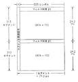
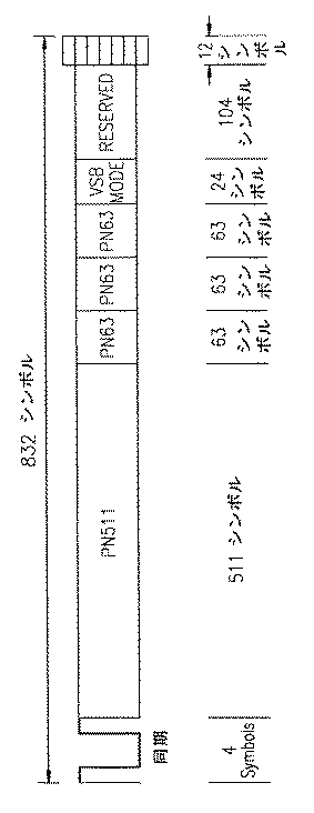
図1は、VSB信号のデータフレームの構造を示す図面である。
1つのデータフレームは2つのフィールドで構成される。1つのフィールドは313個のセグメントで構成される。データフレームの基本単位であるセグメントは832個のシンボルを具備し、各セグメントの開始部分には4個のシンボルよりなるセグメント同期信号がある。
1つのフィールドの最初のセグメントはフィールド同期信号であって、送受信側で既知の一定のパターンを有している。フィールド同期信号は周期的に発生する。1つのフィールドでフィールド同期信号を含む第1のセグメントを除外した残りの312個のセグメントには実際的な情報を含むデータが存在する。
FIG. 1 is a diagram illustrating the structure of a data frame of a VSB signal.
One data frame is composed of two fields. One field is composed of 313 segments. A segment which is a basic unit of a data frame has 832 symbols, and a segment synchronization signal composed of 4 symbols is provided at the start of each segment.
The first segment of one field is a field synchronization signal, and has a certain pattern known on the transmission / reception side. The field sync signal is generated periodically. Data including practical information exists in the remaining 312 segments excluding the first segment including the field synchronization signal in one field.
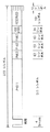
図2は、図1のフィールド同期信号の構造を示す図である。
1つのフィールド同期信号にはPN511信号、3個のPN63信号、VSBモード信号が存在する。フィールド同期信号は1つのフィールド毎に繰り返されるので、PN511信号、3個のPN63信号、VSBモード信号もフィールド毎に繰り返される。
FIG. 2 is a diagram showing the structure of the field synchronization signal of FIG.
One field synchronization signal includes a PN511 signal, three PN63 signals, and a VSB mode signal. Since the field synchronization signal is repeated for each field, the PN511 signal, the three PN63 signals, and the VSB mode signal are also repeated for each field.
図3は、高鮮明テレビの受信システムを示すブロック図である。
図3を参照して受信システム300の搬送波受信過程を説明する。アンテナを介して受信された搬送波信号はチューナ310に印加される。チューナ310は受信された搬送波信号を固定された局部発振信号(図示せず)に応答して一定帯域を有する信号に変換する。
チューナ310から出力される信号はSAW(Surface Acoustic Wave)フィルタによって一定の帯域幅の信号にフィルタリングされる。SAWフィルタ320は一定の帯域幅の信号のみを通過させるので、搬送波信号の歪みのひどい場合にはパイロット信号がSAWフィルタ320の帯域幅の外に存在する。この場合、搬送波復旧装置350はパイロット信号を探し出すことが出来ず、搬送波復旧は不可能になる。
FIG. 3 is a block diagram showing a high-definition television reception system.
A carrier wave receiving process of the
A signal output from the
SAWフィルタ320から出力される信号はIF増幅器330で増幅された後、アナログ・デジタル変換器340によってデジタル信号に復調され、シンボルタイミング復調器360によって標本化時点が検出される。
そして、デジタル信号に変換された信号INSは搬送波復旧装置350によって復元される。この時、搬送波復元ループ370は搬送波信号に存在するパイロット信号を利用して搬送波を復旧するループである。
The signal output from the
Then, the signal INS converted into the digital signal is restored by the carrier
さらに説明すれば、搬送波信号の歪みによってパイロット信号がSAWフィルタ320の帯域幅外に存在すれば、周波数オフセット(すなわち、搬送波周波数の復調周波数間の差)が発生する。周波数オフセットが発生するのは、結局、チューナ310が同調しようとする周波数と実際に同調する周波数とが一致せずに差があるためである。
搬送波復旧装置350及び搬送波復元ループ370は、搬送波信号と復調周波数信号との周波数オフセットを抽出し、まず周波数オフセットを補正するループとして動作する。次に、自動的に位相誤差を補正するループとして動作する。
ところが、送信信号が多重経路を通過する間、種々の原因による雑音によってパイロット信号が弱くなるか、消える場合がある。このような場合、受信システムは搬送波復旧ができなくなる。また、パイロット信号を利用して搬送波復旧をする場合にも、初期に大きな搬送波周波数誤差が存在すると、同期まで長時間を要するという問題がある。
More specifically, if the pilot signal exists outside the bandwidth of the
The
However, while the transmission signal passes through the multipath, the pilot signal may be weakened or disappear due to noise caused by various causes. In such a case, the receiving system cannot recover the carrier wave. Further, even when carrier recovery is performed using a pilot signal, there is a problem that it takes a long time until synchronization if a large carrier frequency error exists in the initial stage.
本発明が解決しようとする技術的課題は、パイロット信号の代わりにVSB信号でフィールド毎に繰り返されるフィールド同期信号に存在するPN63信号を利用して搬送波を正確に、そして迅速に復元できる搬送波復旧装置を提供するところにある。
本発明が解決しようとする他の技術的課題は、パイロット信号の代わりにVSB信号でフィールド毎に繰り返されるフィールド同期信号に存在するPN63信号を利用して搬送波を正確に、そして迅速に復元できる搬送波復旧方法を提供するところにある。
A technical problem to be solved by the present invention is a carrier recovery device that can restore a carrier accurately and quickly using a PN63 signal existing in a field synchronization signal repeated for each field with a VSB signal instead of a pilot signal. Is to provide.
Another technical problem to be solved by the present invention is that a carrier wave that can be accurately and quickly restored using a PN63 signal existing in a field synchronization signal repeated for each field with a VSB signal instead of a pilot signal. It is about to provide a recovery method.
前記技術的課題を達成するための本発明の第1実施例による搬送波復旧装置は、誤差補正部、スイッチ部、スイッチ制御信号発生部、第1誤差検出部及び第2誤差検出部を具備することを特徴とする。
誤差補正部は、実数部分と虚数部分とを有する複素入力信号と周波数信号とを乗じて複素出力信号として出力する。スイッチ部はスイッチ制御信号に応答して前記複素出力信号の出力経路を選択する。
スイッチ制御信号発生部は、パイロット信号の検出結果に応答して前記スイッチ制御信号を発生する。第2誤差検出部は前記スイッチ部を介して前記複素出力信号を受信し、前記複素出力信号に含まれた前記パイロット信号を利用して前記複素出力信号の誤差を復旧して前記周波数信号を出力する。
A carrier recovery apparatus according to a first embodiment of the present invention for achieving the technical problem includes an error correction unit, a switch unit, a switch control signal generation unit, a first error detection unit, and a second error detection unit. It is characterized by.
The error correction unit multiplies the complex input signal having the real part and the imaginary part by the frequency signal and outputs the result as a complex output signal. The switch unit selects an output path of the complex output signal in response to the switch control signal.
The switch control signal generator generates the switch control signal in response to the detection result of the pilot signal. A second error detector configured to receive the complex output signal through the switch unit, recover the error of the complex output signal using the pilot signal included in the complex output signal, and output the frequency signal; To do.
第1誤差検出部は、前記スイッチ部を介して前記複素出力信号及び前記複素出力信号の実数部よりなる実数信号を受信し、前記実数信号から前記複素出力信号に載せられた誤差基準信号の位置を検出し、前記複素出力信号が示す偏角の変化量を測定して前記測定値を誤差信号として前記第2誤差検出部に印加する。
前記技術的課題を達成するための本発明の第2実施例による搬送波復旧装置は、誤差補正部、誤差検出部及び発振器を具備することを特徴とする。
A first error detector configured to receive a real signal composed of the complex output signal and a real part of the complex output signal via the switch unit, and a position of an error reference signal carried on the complex output signal from the real signal; , And the change amount of the declination indicated by the complex output signal is measured, and the measured value is applied as an error signal to the second error detector.
A carrier recovery apparatus according to a second embodiment of the present invention for achieving the technical problem includes an error correction unit, an error detection unit, and an oscillator.
誤差補正部は、実数部分と虚数部分とを有する複素入力信号と周波数信号とを乗じて複素出力信号として出力する。誤差検出部は前記複素出力信号及び前記複素出力信号の実数部よりなる実数信号を受信し、前記実数信号から前記複素出力信号に載せられた誤差基準信号の位置を検出し、前記複素出力信号が示す偏角の変化量を測定して前記測定値を誤差信号として出力する。
発振器は、前記誤差信号に応答して周波数が変化する前記周波数信号を発生する。
The error correction unit multiplies the complex input signal having the real part and the imaginary part by the frequency signal and outputs the result as a complex output signal. The error detector receives a real signal composed of the complex output signal and the real part of the complex output signal, detects a position of an error reference signal carried on the complex output signal from the real signal, and the complex output signal The amount of change of the declination shown is measured and the measured value is output as an error signal.
The oscillator generates the frequency signal whose frequency changes in response to the error signal.
前記技術的課題を達成するための本発明の第3実施例によるデータ信号誤差測定回路は、フィールド同期検出部及び周波数誤差測定部を具備することを特徴とする。
フィールド同期検出部は、複素数形態のデータ信号の実数部よりなる実数信号から前記データ信号に載せられる誤差基準信号の始終の位置を検出する。
周波数誤差測定部は、前記データ信号を受信し、前記フィールド同期検出部の出力に応答して前記データ信号の1つのフレーム毎に繰り返される前記誤差基準信号の位置変化量を利用して前記データ信号が示す偏角の変化量を測定し、前記測定値を誤差信号として出力する。
A data signal error measurement circuit according to a third embodiment of the present invention for achieving the technical problem includes a field synchronization detection unit and a frequency error measurement unit.
The field synchronization detection unit detects the start and end positions of the error reference signal carried on the data signal from the real signal composed of the real part of the data signal in the complex number form.
The frequency error measurement unit receives the data signal, and uses the positional change amount of the error reference signal repeated for each frame of the data signal in response to the output of the field synchronization detection unit. Is measured, and the measured value is output as an error signal.
前記他の技術的課題を達成するための本発明の第1実施例による複素高鮮明テレビ信号の搬送波復旧方法は、前記複素高鮮明テレビ信号にパイロット信号の存否を検出する段階及び前記複素高鮮明テレビ信号にパイロット信号の存否により、前記複素高鮮明テレビ信号に第1誤差検出方法を適用するか、または第2誤差検出方法を適用する段階を具備する。
前記複素高鮮明テレビ信号の搬送波復旧方法は、誤差基準信号を具備する複素出力信号を発生するために前記複素高鮮明テレビ信号と周波数信号とを結合する段階をさらに具備し、前記第1誤差検出方法は前記複素出力信号の実数部に応答して前記複素出力信号が具備する誤差基準信号の位置を決定する段階、前記複素出力信号が具備する前記誤差基準信号の位置に応答して誤差信号を発生する段階及び前記誤差信号に応答して変化する周波数を有する周波数信号を発生する段階を具備する。
According to another aspect of the present invention, there is provided a method for recovering a carrier wave of a complex high-definition television signal according to a first embodiment of the present invention. Depending on whether a pilot signal is present in the television signal, the first error detection method is applied to the complex high definition television signal, or the second error detection method is applied.
The method of recovering a carrier wave of a complex high-definition television signal further comprises combining the complex high-definition television signal and a frequency signal to generate a complex output signal having an error reference signal, and the first error detection. The method determines the position of an error reference signal included in the complex output signal in response to a real part of the complex output signal, and outputs an error signal in response to the position of the error reference signal included in the complex output signal. Generating and generating a frequency signal having a frequency that changes in response to the error signal.
前記他の技術的課題を達成するための本発明の第2実施例による複素高鮮明テレビ信号の搬送波復旧方法は、誤差基準信号を具備する複素出力信号を発生するために前記複素高鮮明テレビ信号と周波数信号とを結合する段階、前記複素出力信号の実数部に応答して前記複素出力信号が具備する誤差基準信号の位置を決定する段階、前記複素出力信号が具備する前記誤差基準信号の位置に応答して誤差信号を発生する段階及び前記誤差信号に応答して変化する周波数を有する周波数信号を発生する段階を具備する。 According to a second embodiment of the present invention, there is provided a complex high-definition television signal carrier recovery method for generating the complex output signal having an error reference signal. And a frequency signal, determining a position of an error reference signal included in the complex output signal in response to a real part of the complex output signal, and a position of the error reference signal included in the complex output signal And generating a frequency signal having a frequency that varies in response to the error signal.
本発明による搬送波復旧装置及び方法は、多様な雑音などによってVSB信号からパイロット信号が検出できない場合にも、VSB信号でフィールド毎に繰り返されるフィールド同期信号に存在するPN63信号を利用して搬送波を正確でかつ迅速に復元できる長所がある。 The carrier recovery apparatus and method according to the present invention uses the PN63 signal present in the field synchronization signal repeated for each field in the VSB signal even when the pilot signal cannot be detected from the VSB signal due to various noises. And there is an advantage that can be restored quickly.
本発明と本発明の動作上の利点及び本発明の実施によって達成される目的を十分に理解するためには、本発明の望ましい実施例を例示する図面及び図面に記載された内容を参照せねばならない。
以下、図面を参照して本発明の望ましい実施例を説明することによって、本発明を詳細に説明する。各図面に付された同一参照符号は同一部材を示す。
図4は、本発明による搬送波復旧装置を示すブロック図である。
図5は、図4の周波数誤差測定部を示すブロック図である。
図4及び図5を参照すれば、本発明の第1実施例による搬送波復旧装置400は誤差補正部410、スイッチ部415、スイッチ制御信号発生部420、第1誤差検出部425及び第2誤差検出部440を具備する。
For a full understanding of the invention, its operational advantages, and the objectives achieved by the practice of the invention, reference should be made to the drawings illustrating the preferred embodiments of the invention and the contents described in the drawings. Don't be.
Hereinafter, the present invention will be described in detail by describing preferred embodiments of the present invention with reference to the drawings. The same reference numerals in the drawings denote the same members.
FIG. 4 is a block diagram showing a carrier recovery apparatus according to the present invention.
FIG. 5 is a block diagram illustrating the frequency error measurement unit of FIG.
4 and 5, the
誤差補正部410は、実数部分と虚数部分とを有する複素入力信号COMISと所定の第2誤差検出部440から出力される周波数信号FRQSとを乗じて複素出力信号COMOSとして出力する。
複素入力信号COMISは入力信号INSが複素フィルタ405によって複素信号形態に変換された信号である。入力信号INSはアンテナを通じて受信された搬送波信号が図3のアナログ・デジタル変換器340を介して出力される実数信号である。搬送波復旧装置400は米国8−レベルVSB HDTVの受信システムの一部に使用することが出来る。したがって、複素入力信号COMISはVSB信号が複素数形態に変換された信号である。
The
The complex input signal COMIS is a signal obtained by converting the input signal INS into a complex signal form by the
複素入力信号COMISは誤差を有しており、複素入力信号COMISと周波数信号FRQSとは乗じられて複素出力信号COMOSが発生する。複素入力信号COMISと周波数信号FRQSとが乗じられて発生する複素出力信号COMOSは複素入力信号COMISの誤差が相殺された信号である。周波数信号FRQSは第1誤差検出部425または第2誤差検出部440が動作されれば、第2誤差検出部440内部の発振器455から発生する。第1誤差検出部425及び第2誤差検出部440の動作は後述する。
The complex input signal COMMIS has an error, and the complex input signal COMMIS and the frequency signal FRQS are multiplied to generate a complex output signal COMOS. The complex output signal COMOS generated by multiplying the complex input signal COMIS and the frequency signal FRQS is a signal in which an error of the complex input signal COMMIS is canceled. The frequency signal FRQS is generated from the
複素入力信号COMISが、最初、誤差補正部410に印加される時には周波数信号FRQSの発生前なので、誤差が相殺された複素出力信号COMOSは発生せず、複素入力信号COMISがそのまま複素出力信号COMOSとして出力される。誤差補正部410は乗算器で構成することができる。
スイッチ制御信号発生部420はパイロット信号の検出結果に応答してスイッチ制御信号SWCONSを発生する。さらに説明すれば、スイッチ制御信号SWCONSは複素出力信号COMOSに含まれたパイロット信号が検出されなければ、複素出力信号COMOSを第1誤差検出部425に印加し、パイロット信号が検出されれば、複素出力信号COMOSを第2誤差検出部440に印加する。
When the complex input signal COMMIS is first applied to the
Switch
スイッチ部415はスイッチ制御信号SWCONSに応答して複素出力信号COMOSを第1誤差検出部425に印加するか、または第2誤差検出部440に印加する。
複素出力信号COMOSにパイロット信号が載せられる場合、複素出力信号COMOSは第2誤差検出部440に印加される。第2誤差検出部440は複素出力信号COMOSを受信し、複素出力信号COMOSに含まれたパイロット信号を利用して複素出力信号COMOSの誤差を復旧する。
The
When a pilot signal is put on the complex output signal COMOS, the complex output signal COMOS is applied to the second
第2誤差検出部440は複素出力信号COMOSに含まれたパイロット信号の周波数誤差と位相誤差とを検出する周波数−位相同期ループ445、周波数−位相同期ループ445の出力をフィルタリングするループフィルタ450及びループフィルタ450の出力または誤差信号OFFSETSに応答して周波数が変化する周波数信号FRQSを発生する発振器455を具備する。第2誤差検出部440の動作は従来の搬送波復旧装置の動作と同一なので詳細説明は省略する。
The
パイロット信号が複素出力信号COMOSで検出されない場合、スイッチ部415はスイッチ制御信号SWCONSに応答して複素出力信号COMOSを第1誤差検出部425に印加する。
第1誤差検出部425は複素出力信号COMOS及び複素出力信号の実数部よりなる実数信号REALSを受信し、実数信号REALSから複素出力信号COMOSに載せられる誤差基準信号の位置を検出し、複素出力信号COMOSが示す偏角の変化量を測定して前記測定値を誤差信号OFFSETSとして第2誤差検出部440の発振器455に印加する。
When the pilot signal is not detected by the complex output signal COMOS, the
The
誤差基準信号は複素入力信号COMISのフィールド同期信号に存在するPN63信号である。
第1誤差検出部425はパイロット信号の代わりに複素出力信号COMOSに存在するフィールド同期信号のPN63信号を利用して複素出力信号COMOSの周波数オフセットを検出する。すなわち、フィールド同期信号は24.2ms毎に繰り返され、フィールド同期信号毎に3個のPN63信号を具備する。
そして、フィールド同期信号が繰り返される毎に、3個のPN63信号のうち2番目のPN63信号の符号が遷移する。すなわち、48.4ms毎に同じPN63信号のうち2番目のPN63信号が同じ符号を有するので、これを利用して複素出力信号COMOSの周波数オフセットが推定できる。
The error reference signal is a PN63 signal present in the field synchronization signal of the complex input signal COMIS.
The
Each time the field synchronization signal is repeated, the sign of the second PN63 signal among the three PN63 signals changes. That is, since the second PN63 signal of the same PN63 signal has the same sign every 48.4 ms, the frequency offset of the complex output signal COMOS can be estimated using this.
フィールド同期信号の検出はフィールド同期検出部430で行われ、複素出力信号COMOSの周波数オフセットの推定は周波数誤差測定部435で行われる。
フィールド同期検出部430は実数信号REALSから前記誤差基準信号の始終の位置を検出する。すなわち、フィールド同期検出部430は複素出力信号COMOSに存在するフィールド同期信号のPN63信号の位置を検出し、その情報を周波数誤差測定部435に出力FSOする。VSB信号からフィールド同期信号を検出し、フィールド同期信号に存在するPN63信号を検出する方法は当業者に周知なので詳細説明は省略する。
周波数誤差測定部435は複素出力信号COMOSを受信し、フィールド同期検出部430の出力FSOに応答して複素出力信号COMOSの1つのフレーム毎に繰り返される前記誤差基準信号の位置変化量を利用して複素出力信号COMOSが示す偏角の変化量を測定し、測定値を誤差信号OFFSETSとして出力する。
The field synchronization signal is detected by the field synchronization detection unit 430, and the frequency offset of the complex output signal COMOS is estimated by the frequency
The field synchronization detection unit 430 detects the start and end positions of the error reference signal from the real number signal REALS. That is, the field synchronization detection unit 430 detects the position of the PN63 signal of the field synchronization signal present in the complex output signal COMOS, and outputs the information to the frequency
The frequency
周波数誤差測定部435は、
The frequency
y(n)は複素出力信号COMOSを示し、y(n+L)は複素出力信号COMOSの周期をLだけ遅延させる信号であり、y(n)*は前記複素出力信号COMOSの共役信号を示し、Lは前記誤差基準信号のサンプル長である。PN63信号のサンプル長は63であるので、Lは63である。
y (n) indicates a complex output signal COMOS, y (n + L) is a signal that delays the cycle of the complex output signal COMOS by L, y (n) * indicates a conjugate signal of the complex output signal COMOS, and L Is the sample length of the error reference signal. Since the sample length of the PN63 signal is 63, L is 63.
数式1は結局周波数誤差測定部435に入力される信号、すなわち、複素出力信号COMOSの位相を測定する式である。複素平面で複素出力信号COMOSが実数軸となす位相、すなわち偏角を測定して偏角の変化量を計算すれば、その値は複素出力信号COMOSの周波数オフセットの変化量になる。すなわち複素出力信号COMOSの周波数誤差となる。
数式1で複素出力信号COMOSの周期をLだけ遅延させたy(n+L)に複素出力信号COMOSの共役信号のy(n)*を乗じた結果を、nが0からL−1まで加え続ける過程は相関演算と同一である。相関演算は本発明の技術分野で当業者に周知なので詳細説明は省略する。
Equation 1 is an equation for measuring the phase of the signal input to the frequency
A process in which n is continuously added from 0 to L−1 by multiplying y (n + L) obtained by delaying the cycle of the complex output signal COMOS by L in Expression 1 and y (n) * of the conjugate signal of the complex output signal COMOS. Is the same as the correlation calculation. Since the correlation calculation is well known to those skilled in the art in the technical field of the present invention, detailed description thereof is omitted.
周波数誤差測定部435は前記数式に対応する演算を遂行するために、複素出力信号COMOSを受信して複素出力信号COMOSの周期をLだけ遅延させる遅延部510、複素出力信号COMOSを受信して共役複素出力信号を発生させる共役信号発生部520、遅延部510の出力と共役複素出力信号とを乗じる第1乗算器530、第1乗算器530の出力のうち虚数部のみを抽出する虚数部発生器540、第1乗算器530の出力のうち実数部を抽出し、抽出された実数部の逆数を発生する実数部発生器550、虚数部発生器540の出力と実数部発生器550の出力とを乗じる第2乗算器560、第2乗算器560の出力のアークタンジェント値を求める演算部570及び演算部570の出力に所定の係数信号COFSを乗じて誤差信号OFFSETSを発生する第3乗算器580を具備する。係数信号COFSは1/(2*π*L)であり、ここでLは誤差基準信号のサンプル長であることを特徴とする。
The frequency
周波数誤差測定部435の構成要素は数式1の演算を実行するためのものであり、数式1による機能を実行するので詳細説明は省略する。
周波数誤差測定部435で発生した誤差信号OFFSETSは第2誤差検出部440の発振器455に印加される。発振器455は数値制御発振器である。発振器455は誤差信号OFFSETSに応答して周波数信号FRQSを発生する。誤差補正部410は周波数信号FRQSと複素入力信号COMISとを乗じて誤差が除去された複素出力信号COMOSを発生する。誤差が完全に除去された複素出力信号COMOSが発生するまで複素出力信号COMOSは、第1誤差検出部425と発振器455及び誤差補正部410のループを通過し続ける。誤差が完全に除去された複素出力信号COMOSは搬送波復旧装置400の外部に出力される。
The constituent elements of the frequency
The error signal OFFSETS generated by the frequency
スイッチ制御信号SWCONSは、最初入力される複素出力信号COMOSを第1誤差検出部425に印加し、以後に入力される複素出力信号COMOSを第2誤差検出部440に印加することができる。この場合、最初入力される複素出力信号COMOSは第1誤差検出部425に印加され、前述した過程によって誤差信号OFFSETSが発生する。
発生した誤差信号OFFSETSは発振器455に印加され、発振器455から出力された周波数信号FRQSは複素入力信号COMISと乗じられて複素出力信号COMOSとして出力される。出力された複素出力信号COMOSは第2誤差検出部440に印加される。第2誤差検出部440は従来の搬送波復旧装置と同じ動作をし、搬送波復旧のための位相同期を実行する。
The switch control signal SWCONS can apply a complex output signal COMOS that is input first to the first
The generated error signal OFFSETS is applied to the
すなわち、最初に、複素出力信号COMOSが印加されれば、第1誤差検出部425を利用して誤差検出及び補正をし、次に複素出力信号COMOSが印加されれば、第2誤差検出部440を利用して周波数誤差検出及び位相誤差検出を実行する。したがって、第2誤差検出部440と同じ構成を有する従来の搬送波復旧装置だけを利用して搬送波復旧を行うよりもさらに迅速に誤差検出及び搬送波復旧を実行することが出来る。
That is, first, when the complex output signal COMOS is applied, error detection and correction are performed using the first
図6は、他の技術的課題を達成するための本発明の第1実施例による搬送波復旧方法を説明するフローチャートである。
図7は、図6の第1誤差検出方法を説明するフローチャートである。
図8は、図7の誤差信号発生方法を説明するフローチャートである。
FIG. 6 is a flowchart illustrating a carrier recovery method according to the first embodiment of the present invention for achieving another technical problem.
FIG. 7 is a flowchart for explaining the first error detection method of FIG.
FIG. 8 is a flowchart for explaining the error signal generation method of FIG.
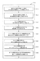
図4乃至図8を参照して複素入力信号の誤差を検出して補正する高鮮明テレビの搬送波復旧方法を説明する。
まず、複素入力信号からパイロット信号が検出されなければ、第1誤差検出方法を選択し、パイロット信号が検出されれば、第2誤差検出方法を選択する。(610段階)
610段階で、複素出力信号は複素入力信号と同じ信号であり、複素入力信号はVSB信号が複素数形態に変換された信号である。
第1誤差検出方法が選択されれば、複素入力信号と同じ信号の複素出力信号及び複素出力信号の実数部よりなる実数信号を受信し、この実数信号から複素出力信号に載せられる誤差基準信号の位置を検出し、複素出力信号が示す偏角の変化量を測定してこの測定値を誤差信号として発生する(620段階)。
With reference to FIGS. 4 to 8, a method for restoring a carrier wave of a high-definition television set that detects and corrects an error of a complex input signal will be described.
First, if the pilot signal is not detected from the complex input signal, the first error detection method is selected. If the pilot signal is detected, the second error detection method is selected. (Step 610)
In
If the first error detection method is selected, a real signal composed of a complex output signal having the same signal as the complex input signal and a real part of the complex output signal is received, and an error reference signal put on the complex output signal from the real signal is received. The position is detected, the amount of change in the deflection angle indicated by the complex output signal is measured, and this measured value is generated as an error signal (step 620).
620段階を詳しく説明する。実数信号から誤差基準信号の始終の位置を検出する(710段階)。誤差基準信号は複素出力信号のフィールド同期信号に存在するPN63信号である。710段階の動作は図4のフィールド同期検出部430の動作と同一であるので詳細説明は省略する。
複素出力信号を受信し、710段階の検出結果に応答して複素出力信号の1つのフレーム毎に繰り返される誤差基準信号の位置変化量を利用して複素出力信号が示す偏角の変化量を測定し、この測定値を誤差信号として出力する(720段階)。複素出力信号の偏角の変化量を計算すれば、その値は複素出力信号COMOSの周波数オフセットの変化量になる。これは、すなわち複素出力信号COMOSの周波数誤差となる。
Step 620 will be described in detail. First and last positions of the error reference signal are detected from the real signal (step 710). The error reference signal is a PN63 signal present in the field synchronization signal of the complex output signal. Since the operation in
The complex output signal is received, and the change amount of the deflection angle indicated by the complex output signal is measured by using the positional change amount of the error reference signal that is repeated for each frame of the complex output signal in response to the detection result of 710 steps. The measured value is output as an error signal (step 720). If the change amount of the deviation angle of the complex output signal is calculated, the value becomes the change amount of the frequency offset of the complex output signal COMOS. This is a frequency error of the complex output signal COMOS.
720段階の動作を詳しく説明する。複素出力信号を受信して複素出力信号の周期をLだけ遅延させる(810段階)。複素出力信号を受信して共役複素出力信号を発生させる(820段階)。810段階の出力と共役複素出力信号とを乗じる(830段階)。830段階の出力のうち虚数部のみを抽出する(840段階)。830段階の出力のうち実数部を抽出し、抽出された実数部の逆数を発生する(850段階)。840段階の出力と850段階の出力とを乗じる(860段階)。860段階の出力のアークタンジェント値を求める(870段階)。870段階の出力に所定の係数信号を乗じて誤差信号を発生する(880段階)。係数信号は1/(2*π*L)であり、ここで前記Lは誤差基準信号のサンプル長である。
The operation in
810乃至860段階は、誤差基準信号のサンプル長だけ繰り返される。すなわち、L回だけ繰り返される。810乃至880段階は前述した数式1を計算する方法である。
810乃至860段階をL回繰り返し、その結果を加え続ける過程は相関演算と同一である。相関演算は本発明の技術分野の当業者には周知であるから詳細説明は省略する。複素出力信号の偏角の変化量は、結局、複素出力信号の周波数誤差と同一である。
720段階の動作は図4の周波数誤差測定部435の動作と同一である。したがって、詳細説明は省略する。
The process of repeating
The operation in
誤差信号に応答して周波数が変化する周波数信号を発生する(630段階)。630段階は図4の発振器455の動作である。周波数信号は複素入力信号と乗じられて複素入力信号の周波数誤差を相殺できる信号である。周波数信号と複素入力信号とを乗じて誤差が補正された前記複素出力信号を発生する(670段階)。誤差が補正された複素出力信号は搬送波復旧装置の外部に出力される。
610段階で第2検出方法が選択されれば、複素入力信号と同じ信号の複素出力信号に含まれたパイロット信号の周波数誤差と位相誤差とを検出する(640段階)。640段階の出力をフィルタリングする(650段階)。650段階の出力に応答して周波数信号を発生し、670段階に戻る(660段階)。複素出力信号COMOSでパイロット信号が検出されれば、第2検出方法が選択される。第2検出方法は図4の第2誤差検出部440で遂行される動作と同一である。したがって、詳細説明は省略する。
A frequency signal whose frequency changes in response to the error signal is generated (step 630). Step 630 is the operation of the
If the second detection method is selected in
図9は、本発明の第2実施例による搬送波復旧装置を示すブロック図である。
図10は、他の技術的課題を達成するための本発明の第2実施例による搬送波復旧方法を説明するフローチャートである。
図11は、図10の誤差信号発生方法を説明するフローチャートである。
FIG. 9 is a block diagram illustrating a carrier recovery apparatus according to a second embodiment of the present invention.
FIG. 10 is a flowchart illustrating a carrier recovery method according to a second embodiment of the present invention for achieving another technical problem.
FIG. 11 is a flowchart for explaining the error signal generation method of FIG.
図9乃至図11を参照して搬送波復旧装置及び方法を詳細に説明する。
高鮮明テレビの搬送波復旧方法1000は、まず前記複素入力信号と同じ信号の複素出力信号及び複素出力信号の実数部よりなる実数信号を受信し、この実数信号から複素出力信号に載せられる誤差基準信号の位置を検出し、複素出力信号が示す偏角の変化量を測定して測定値を誤差信号として発生する(1010段階)。
1010段階は、第2実施例による搬送波復旧装置900の誤差検出部915で行われる動作である。
搬送波復旧装置900は誤差補正部910、誤差検出部915及び発振器930を具備する。
The carrier recovery apparatus and method will be described in detail with reference to FIGS.
The high-definition television
The
デジタル信号に変換された搬送波信号は入力信号INSであって、複素フィルタ905に入力される。複素フィルタ905は入力信号INSを複素数形態の信号の複素入力信号COMISに転換させる。複素入力信号COMISは誤差が補正される前には複素出力信号COMOSとして誤差検出部915に印加される。この時、複素出力信号COMOSの実数部よりなる実数信号REALSも誤差検出部915に印加される。
1010段階は実数信号から誤差基準信号の始終の位置を検出する段階(1110段階)及び複素出力信号を受信し、1110段階の検出結果に応答して複素出力信号の1つのフレーム毎に繰り返される誤差基準信号の位置変化量を利用して複素出力信号が示す偏角の変化量を測定し、この測定値を誤差信号として出力する段階(1120段階)を具備する。
The carrier signal converted into the digital signal is an input signal INS and is input to the
1110段階乃至1120段階は誤差検出部915のフィールド同期検出部920及び周波数誤差測定部925で実行される動作である。
誤差検出部915は第1実施例の第1誤差検出部425と同じ回路構成を有する。したがって、周波数誤差測定部925は図5に示された構成要素が具備できる。誤差検出部915の動作も第1誤差検出部425と同一であるので、動作の詳細なる説明は省略する。
誤差検出部915から出力される誤差信号に応答して周波数が変化する周波数信号を発生する(1020段階)。周波数信号FRQSは発振器930で発生する。周波数信号FRQSは複素入力信号COMISと乗じられて複素入力信号COMISの誤差が相殺できる信号である。
周波数信号と複素入力信号とを乗じて誤差が補正された複素出力信号を発生する(1030段階)。誤差補正部910は複素入力信号COMISと周波数信号FRQSとを乗じて誤差が補正された複素出力信号COMOSを発生する。複素出力信号COMOSは搬送波復旧装置900の外部に出力される。
The
A frequency signal whose frequency changes in response to the error signal output from the
The complex output signal is generated by multiplying the frequency signal and the complex input signal (step 1030). The
本発明の第3実施例によるデータ信号誤差測定回路について説明する。
第3実施例によるデータ信号誤差測定回路は図4の第1誤差検出部425と同じ回路構成を有する。したがって、以下では図4を参照して説明する。
データ信号誤差測定回路425はフィールド同期検出部430及び周波数誤差測定部435を具備する。データ信号誤差測定回路425は入力されるデータ信号の誤差を検出する回路である。データ信号はVSB信号が複素数形態に変換された信号でありうる。VSB信号にはフィールド同期信号がフィールド毎に繰り返される。フィールド同期信号には3個のPN63信号が存在する。
A data signal error measuring circuit according to a third embodiment of the present invention will be described.
The data signal error measurement circuit according to the third embodiment has the same circuit configuration as the first
The data signal
データ信号誤差測定回路425は3個のPN63信号を利用して、入力されるデータ信号の誤差を測定して誤差信号OFFSETSを発生する。データ信号誤差測定回路425はフィールド同期検出部430と周波数誤差測定部435とを具備する。
フィールド同期検出部430は複素数形態のデータ信号COMOSの実数部よりなる実数信号REALSからデータ信号COMOSに載せられる誤差基準信号の始終の位置を検出する。誤差基準信号はデータ信号COMOSのフィールド同期信号に存在するPN63信号である。
The data signal
The field synchronization detection unit 430 detects the start and end positions of the error reference signal carried on the data signal COMOS from the real number signal REALS made up of the real part of the complex number data signal COMOS. The error reference signal is a PN63 signal present in the field synchronization signal of the data signal COMOS.
周波数誤差測定部435はデータ信号COMOSを受信し、フィールド同期検出部430の出力FSOに応答してデータ信号COMOSの1つのフレーム毎に繰り返される誤差基準信号の位置変化量を利用してデータ信号COMOSが示す偏角の変化量を測定し、測定値を誤差信号OFFSETSとして出力する。
さらに説明すれば、周波数誤差測定部435は図5に示された回路構成を有しうる。周波数誤差測定部435の動作は前述したので、詳細説明は省略する。データ信号誤差測定回路425を利用すれば、入力されるVSB信号からパイロット信号が検出できなくても、VSB信号に存在するPN63信号から入力されるVSB信号に存在する誤差が求められる。
The frequency
More specifically, the frequency
以上のように、図面と明細書で最適の実施例が開示された。ここで特定な用語が使われたが、これは単に本発明を説明するための目的で使われており、意味限定や特許請求の範囲に記載された本発明の範囲を制限するために使われたものではない。したがって、本技術分野の当業者であれば、これより多様な変形及び均等な他の実施例が可能である点が理解できるであろう。したがって、本発明の真の技術的保護範囲は特許請求の範囲の技術的思想によって定められねばならない。 As described above, the optimum embodiment has been disclosed in the drawings and specification. Although specific terminology has been used herein, it is used merely for the purpose of describing the present invention and is intended to limit the scope of the invention as defined in the meaning and claims. Not a thing. Accordingly, those skilled in the art will appreciate that various modifications and other equivalent embodiments are possible. Therefore, the true technical protection scope of the present invention must be determined by the technical idea of the claims.
本発明は、高鮮明テレビの受信システム分野に利用でき、特に高鮮明テレビの搬送波復旧装置に利用できる。 INDUSTRIAL APPLICABILITY The present invention can be used in the field of reception systems for high-definition television, and in particular, can be used for carrier recovery devices for high-definition television.
400 搬送波復旧装置
405 複素フィルタ
410 誤差補正部
415 スイッチ部
420 スイッチ制御信号発生部
425 第1誤差検出部
430 フィールド同期検出部
435 周波数誤差測定部
440 第2誤差検出部
445 周波数−位相同期ループ
450 ループフィルター
455 発振器
INS 入力信号
COMIS 複素入力信号
COMOS 複素出力信号
SWCONS スイッチ制御信号
FRQS 周波数信号
REALS 実数信号
OFFSETS 誤差信号
400
Claims (30)
スイッチ制御信号に応答して前記複素出力信号の出力経路を選択するスイッチ部と、
パイロット信号の検出結果に応答して前記スイッチ制御信号を発生させるスイッチ制御信号発生部と、
前記スイッチ部を介して前記複素出力信号を受信し、前記複素出力信号に含まれた前記パイロット信号を利用して前記複素出力信号の誤差を復旧して前記周波数信号を発生する第2誤差検出部と、
前記スイッチ部を介して前記複素出力信号及び前記複素出力信号の実数部よりなる実数信号を受信し、前記実数信号から前記複素出力信号に載せられる誤差基準信号の位置を検出し、前記複素出力信号が示す偏角の変化量を測定して前記測定値を誤差信号として前記第2誤差検出部に印加する第1誤差検出部と、
を具備することを特徴とする高鮮明テレビの搬送波復旧装置。 An error correction unit that outputs a complex output signal by multiplying a complex input signal having a real part and an imaginary part by a frequency signal;
A switch unit that selects an output path of the complex output signal in response to a switch control signal;
A switch control signal generator for generating the switch control signal in response to a detection result of the pilot signal;
A second error detection unit that receives the complex output signal via the switch unit, recovers an error of the complex output signal using the pilot signal included in the complex output signal, and generates the frequency signal When,
The complex output signal and a real signal composed of the real part of the complex output signal are received via the switch unit, the position of the error reference signal carried on the complex output signal is detected from the real signal, and the complex output signal is detected. A first error detection unit that measures the amount of change in the declination indicated by and applies the measurement value as an error signal to the second error detection unit;
A high-definition television carrier recovery apparatus comprising:
前記実数信号から前記誤差基準信号の始終の位置を検出するフィールド同期検出部と、
前記複素出力信号を受信し、前記フィールド同期検出部の出力に応答して前記複素出力信号の1つのフレーム毎に繰り返される前記誤差基準信号の位置変化量を利用して前記複素出力信号が示す偏角の変化量を測定し、前記測定値を前記誤差信号として出力する周波数誤差測定部と、
を具備することを特徴とする請求項1に記載の高鮮明テレビの搬送波復旧装置。 The first error detector is
A field synchronization detection unit for detecting the start and end positions of the error reference signal from the real signal;
The complex output signal is received, and a deviation indicated by the complex output signal is obtained by using a positional change amount of the error reference signal repeated for each frame of the complex output signal in response to an output of the field synchronization detection unit. A frequency error measurement unit that measures the amount of change in angle and outputs the measurement value as the error signal;
The carrier recovery device for a high-definition television set according to claim 1.
前記複素出力信号を受信して前記複素出力信号の周期をLだけ遅延させる遅延部と、
前記複素出力信号を受信して共役複素出力信号を発生させる共役信号発生部と、
前記遅延部の出力と前記共役複素出力信号とを乗じる第1乗算器と、
前記第1乗算器の出力のうち虚数部のみを抽出する虚数部発生器と、
前記第1乗算器の出力のうち実数部を抽出し、抽出された前記実数部の逆数を発生する実数部発生器と、
前記虚数部発生器の出力と前記実数部発生器の出力とを乗じる第2乗算器と、
前記第2乗算器の出力のアークタンジェント値を求める演算部と、
前記演算部の出力に所定の係数信号を乗じて前記誤差信号を発生する第3乗算器と、を具備することを特徴とする請求項2に記載の高鮮明テレビの搬送波復旧装置。 The frequency error measurement unit includes:
A delay unit that receives the complex output signal and delays the period of the complex output signal by L;
A conjugate signal generator for receiving the complex output signal and generating a conjugate complex output signal;
A first multiplier for multiplying the output of the delay unit and the conjugate complex output signal;
An imaginary part generator for extracting only the imaginary part of the output of the first multiplier;
A real part generator for extracting a real part from an output of the first multiplier and generating a reciprocal of the extracted real part;
A second multiplier for multiplying the output of the imaginary part generator and the output of the real part generator;
An arithmetic unit for obtaining an arc tangent value of the output of the second multiplier;
3. The carrier recovery device for a high-definition television according to claim 2, further comprising: a third multiplier that multiplies an output of the arithmetic unit by a predetermined coefficient signal to generate the error signal.
1/(2*π*L)であり、ここで前記Lは、
前記誤差基準信号のサンプル長であることを特徴とする請求項3に記載の高鮮明テレビの搬送波復旧装置。 The coefficient signal is
1 / (2 * π * L), where L is
4. The high-definition television carrier recovery apparatus according to claim 3, wherein the error reference signal has a sample length.
y(n)は前記複素出力信号を示し、y(n+L)は前記複素出力信号の周期をLだけ遅延させた信号であり、y(n)*は前記複素出力信号の共役信号を示し、Lは前記誤差基準信号のサンプル長であることを特徴とする請求項2に記載の高鮮明テレビの搬送波復旧装置。 The frequency error measurement unit includes:
y (n) represents the complex output signal, y (n + L) represents a signal obtained by delaying the period of the complex output signal by L, y (n) * represents a conjugate signal of the complex output signal, and L 3. The high-definition television carrier recovery apparatus according to claim 2, wherein is a sample length of the error reference signal.
前記複素出力信号に含まれた前記パイロット信号の周波数誤差と位相誤差とを検出する周波数−位相同期ループと、
前記周波数−位相同期ループの出力をフィルタリングするループフィルタと、
前記ループフィルタの出力または前記誤差信号に応答して周波数が変化する前記周波数信号を発生する発振器と、
を具備することを特徴とする請求項1に記載の高鮮明テレビの搬送波復旧装置。 The second error detector is
A frequency-phase locked loop for detecting a frequency error and a phase error of the pilot signal included in the complex output signal;
A loop filter for filtering the output of the frequency-phase locked loop;
An oscillator for generating the frequency signal whose frequency changes in response to an output of the loop filter or the error signal;
The carrier recovery device for a high-definition television set according to claim 1.
VSB信号が複素数形態に変換された信号であり、
前記誤差基準信号は、
前記複素入力信号のフィールド同期信号に存在するPN63信号であることを特徴とする請求項1に記載の高鮮明テレビの搬送波復旧装置。 The complex input signal is
A signal obtained by converting a VSB signal into a complex form,
The error reference signal is
2. The carrier recovery apparatus for a high-definition television set according to claim 1, wherein the PN63 signal is present in a field synchronization signal of the complex input signal.
前記複素出力信号に含まれた前記パイロット信号が検出されなければ、前記複素出力信号を前記第1誤差検出部に印加し、
前記パイロット信号が検出されれば、前記複素出力信号を前記第2誤差検出部に印加することを特徴とする請求項1に記載の高鮮明テレビの搬送波復旧装置。 The switch control signal is
If the pilot signal included in the complex output signal is not detected, the complex output signal is applied to the first error detector,
The apparatus of claim 1, wherein if the pilot signal is detected, the complex output signal is applied to the second error detection unit.
最初入力される前記複素出力信号を前記第1誤差検出部に印加し、以後に入力される前記複素出力信号を前記第2誤差検出部に印加することを特徴とする請求項1に記載の高鮮明テレビの搬送波復旧装置。 The switch control signal is
2. The high output signal according to claim 1, wherein the complex output signal that is input first is applied to the first error detector, and the complex output signal that is input thereafter is applied to the second error detector. Clear TV carrier recovery device.
前記複素出力信号及び前記複素出力信号の実数部よりなる実数信号を受信し、前記実数信号から前記複素出力信号に載せられる誤差基準信号の位置を検出し、前記複素出力信号が示す偏角の変化量を測定して前記測定値を誤差信号として出力する誤差検出部と、
前記誤差信号に応答して周波数が変化する前記周波数信号を発生する発振器と、
を具備することを特徴とする高鮮明テレビの搬送波復旧装置。 An error correction unit that outputs a complex output signal by multiplying a complex input signal having a real part and an imaginary part by a frequency signal;
Receiving a real signal comprising the complex output signal and a real part of the complex output signal, detecting a position of an error reference signal carried on the complex output signal from the real signal, and changing a declination indicated by the complex output signal An error detector that measures the amount and outputs the measured value as an error signal;
An oscillator for generating the frequency signal whose frequency changes in response to the error signal;
A high-definition television carrier recovery apparatus comprising:
前記実数信号から前記誤差基準信号の始終の位置を検出するフィールド同期検出部と、
前記フィールド同期検出部によって決定される前記誤差基準信号の始終の位置に応答して前記複素出力信号の偏角の変化量を測定し、前記複素出力信号の偏角の変化量に応答して前記誤差信号を出力する周波数誤差測定部と、
を具備することを特徴とする請求項10に記載の高鮮明テレビの搬送波復旧装置。 The error detector is
A field synchronization detection unit for detecting the start and end positions of the error reference signal from the real signal;
Measure the amount of change in the deflection angle of the complex output signal in response to the position of the error reference signal determined by the field synchronization detection unit, and respond to the amount of change in the deflection angle of the complex output signal. A frequency error measurement unit that outputs an error signal;
The carrier recovery device for a high-definition television set according to claim 10.
y(n)は前記複素出力信号を示し、y(n+L)は前記複素出力信号の周期をLだけ遅延させた信号であり、y(n)*は前記複素出力信号の共役信号を示し、Lは前記誤差基準信号のサンプル長であることを特徴とする請求項11に記載の高鮮明テレビの搬送波復旧装置。 The frequency error measurement unit includes:
y (n) represents the complex output signal, y (n + L) represents a signal obtained by delaying the period of the complex output signal by L, y (n) * represents a conjugate signal of the complex output signal, and L 12. The high-definition television carrier recovery apparatus according to claim 11, wherein is a sample length of the error reference signal.
VSB信号が複素数形態に変換された信号であり、
前記誤差基準信号は、
前記複素入力信号のフィールド同期信号に存在するPN63信号であることを特徴とする請求項10に記載の高鮮明テレビの搬送波復旧装置。 The complex input signal is
A signal obtained by converting a VSB signal into a complex form,
The error reference signal is
The high-definition television carrier recovery apparatus according to claim 10, wherein the PN63 signal is present in a field synchronization signal of the complex input signal.
前記複素数形態のデータ信号に存在する誤差基準信号の位置に応答して前記複素数形態のデータ信号の偏角の変化量を測定し、前記複素数形態のデータ信号の偏角の変化量に応答して誤差信号を発生する周波数誤差測定部と、
を具備することを特徴とするデータ信号誤差測定回路。 A field synchronization detection unit for detecting the start and end positions of an error reference signal carried on the data signal from a real signal composed of a real part of the data signal in a complex number;
In response to the position of the error reference signal present in the complex number data signal, the amount of change in the declination of the complex number data signal is measured, and in response to the amount of change in the declination of the complex number data signal A frequency error measurement unit for generating an error signal;
A data signal error measuring circuit comprising:
前記データ信号を受信して前記データ信号の周期をLだけ遅延させる遅延部と、
前記データ信号を受信して共役データ信号を発生させる球額信号発生部と、
前記遅延部の出力と前記共役データ信号を乗じる第1乗算器と、
前記第1乗算器の出力のうち虚数部のみを抽出する虚数部発生器と、
前記第1乗算器の出力のうち実数部を抽出し、抽出された前記実数部の逆数を発生する実数部発生器と、
前記虚数部発生器の出力と前記実数部発生器の出力とを乗じる第2乗算器と、
前記第2乗算器の出力のアークタンジェント値を求める演算部と、
前記演算部の出力に所定の係数信号を乗じて前記誤差信号を発生する第3乗算器と、を具備することを特徴とする請求項15に記載のデータ信号誤差測定回路。 The frequency error measurement unit includes:
A delay unit that receives the data signal and delays the cycle of the data signal by L;
A forehead signal generator for receiving the data signal and generating a conjugate data signal;
A first multiplier for multiplying the output of the delay unit and the conjugate data signal;
An imaginary part generator for extracting only the imaginary part of the output of the first multiplier;
A real part generator for extracting a real part from an output of the first multiplier and generating a reciprocal of the extracted real part;
A second multiplier for multiplying the output of the imaginary part generator and the output of the real part generator;
An arithmetic unit for obtaining an arc tangent value of the output of the second multiplier;
The data signal error measurement circuit according to claim 15, further comprising a third multiplier that multiplies an output of the arithmetic unit by a predetermined coefficient signal to generate the error signal.
1/(2*π*L)であり、ここでLは、
前記誤差基準信号のサンプル長であることを特徴とする請求項17に記載のデータ信号誤差測定回路。 The coefficient signal is
1 / (2 * π * L), where L is
18. The data signal error measurement circuit according to claim 17, wherein the error reference signal has a sample length.
y(n)は前記データ信号を示し、y(n+L)は前記データ信号の周期をLだけ遅延させた信号であり、y(n)*は前記データ信号の共役信号を示し、Lは前記誤差基準信号のサンプル長であることを特徴とする請求項15に記載のデータ信号誤差測定回路。 The frequency error measurement unit includes:
y (n) indicates the data signal, y (n + L) is a signal obtained by delaying the cycle of the data signal by L, y (n) * indicates a conjugate signal of the data signal, and L indicates the error. 16. The data signal error measurement circuit according to claim 15, wherein the data signal error measurement circuit has a sample length of the reference signal.
VSB信号が複素数形態に変換された信号であり、
前記誤差基準信号は、
前記データ信号のフィールド同期信号に存在するPN63信号であることを特徴とする請求項15に記載のデータ信号誤差測定回路。 The data signal is
A signal obtained by converting a VSB signal into a complex form,
The error reference signal is
16. The data signal error measurement circuit according to claim 15, wherein the data signal error measurement circuit is a PN63 signal present in a field synchronization signal of the data signal.
前記複素高鮮明テレビ信号に対してパイロット信号の存否を検出する段階と、
前記パイロット信号の存否によって前記複素高鮮明テレビ信号に第1誤差検出方法と第2誤差検出方法のいずれかを適用して搬送波周波数誤差を検出する段階と、
を具備し、さらに、
誤差基準信号を具備する複素出力信号を発生するために前記複素高鮮明テレビ信号と周波数信号を結合する段階を具備し、
前記第1誤差検出方法は、
前記複素出力信号の実数部に応答して前記複素出力信号が具備する誤差基準信号の位置を決定する段階と、
前記複素出力信号が具備する前記誤差基準信号の位置に応答して誤差信号を発生する段階と、
前記誤差信号に応答して変化する周波数を有する周波数信号を発生する段階と、
を具備し、
前記第2誤差検出方法は、
前記複素高鮮明テレビ信号に含まれた前記パイロット信号の周波数誤差と位相誤差とを検出する段階と、
前記周波数誤差と位相誤差とをフィルタリングする段階と、
前記フィルタリングされた周波数誤差と位相誤差とに応答して前記周波数信号を発生する段階と、
を具備することを特徴とする複素高鮮明テレビ信号の搬送波復旧方法。 In the carrier recovery method for complex high definition television signals,
And detecting the presence or absence of the pilot signal for the complex high sharpness television signal,
And detecting the carrier frequency error by the presence or absence of pre Kipa pilots signals apply one of the first error detecting method and the second error detection methods from the complex high sharpness television signal,
Further comprising
Combining the complex high definition television signal and a frequency signal to generate a complex output signal comprising an error reference signal;
The first error detection method includes:
Determining a position of an error reference signal included in the complex output signal in response to a real part of the complex output signal;
Generating an error signal in response to the position of the error reference signal included in the complex output signal;
Generating a frequency signal having a frequency that varies in response to the error signal;
Comprising
The second error detection method includes:
Detecting a frequency error and a phase error of the pilot signal included in the complex high-definition television signal;
Filtering the frequency error and phase error;
Generating the frequency signal in response to the filtered frequency error and phase error;
A method for recovering a carrier wave of a complex high-definition television signal.
前記実数信号から前記誤差基準信号の始終の位置を検出する段階と、
前記誤差基準信号の始終の位置に応答して前記複素出力信号の偏角の変化量を測定する段階と、
前記複素出力信号の偏角の変化量に応答して前記誤差信号を出力する段階と、
を具備することを特徴とする請求項21に記載の複素高鮮明テレビ信号の搬送波復旧方法。 The first error detection method includes:
Detecting a starting position of the error reference signal from the real signal;
Measuring the amount of change in the deflection angle of the complex output signal in response to the position of the beginning of the error reference signal;
Outputting the error signal in response to the amount of change in the deflection angle of the complex output signal;
The method for recovering a carrier wave of a complex high-definition television signal according to claim 21 .
前記複素出力信号を受信して前記複素出力信号の周期をLだけ遅延させ、遅延された複素出力信号を発生させる段階と、
前記複素出力信号を受信して共役複素出力信号を発生させる段階と、
前記遅延された複素出力信号と前記共役複素出力信号とを乗じて第1勝算出力信号を発生する段階と、
前記第1勝算出力信号の虚数部と前記第1勝算出力信号の実数部の逆数とを乗じて第2勝算値を発生する段階と、
前記第2勝算値のアークタンジェント値を求める段階と、
前記第2勝算値のアークタンジェント値に所定の係数信号を乗じて前記誤差信号を発生する段階と、
を具備することを特徴とする請求項21に記載の複素高鮮明テレビ信号の搬送波復旧方法。 The first error detection method includes:
Receiving the complex output signal and delaying the period of the complex output signal by L to generate a delayed complex output signal ;
Receiving the complex output signal and generating a conjugate complex output signal ;
Multiplying the delayed complex output signal and the conjugate complex output signal to generate a first win calculation force signal ;
Multiplying the imaginary part of the first win calculation force signal by the inverse of the real part of the first win calculation force signal to generate a second win value;
Obtaining an arc tangent value of the second winning value;
Multiplying the arc tangent value of the second winning value by a predetermined coefficient signal to generate the error signal;
The method for recovering a carrier wave of a complex high-definition television signal according to claim 21 .
1/(2*π*L)であり、ここでLは、
前記誤差基準信号のサンプル長であることを特徴とする請求項23に記載の複素高鮮明テレビ信号の搬送波復旧方法。 The coefficient signal is
1 / (2 * π * L), where L is
24. The method of claim 23 , wherein the error reference signal has a sample length .
y(n)は前記複素出力信号を示し、y(n+L)は前記複素出力信号の周期をLだけ遅延させた信号であり、y(n) * は前記複素出力信号の共役信号を示し、Lは前記誤差基準信号のサンプル長であることを特徴とする請求項21に記載の複素高鮮明テレビ信号の搬送波復旧方法。
y (n) represents the complex output signal, y (n + L) represents a signal obtained by delaying the period of the complex output signal by L, y (n) * represents a conjugate signal of the complex output signal, and L The method of claim 21 , wherein is a sample length of the error reference signal.
VSB信号が複素数形態に変換された信号であり、
前記誤差基準信号は、
前記複素入力信号のフィールド同期信号に存在するPN63信号であることを特徴とする請求項21に記載の複素高鮮明テレビ信号の搬送波復旧方法。 The complex input signal is
A signal obtained by converting a VSB signal into a complex form,
The error reference signal is
The method for recovering a carrier wave of a complex high-definition television signal according to claim 21 , wherein the signal is a PN63 signal present in a field synchronization signal of the complex input signal .
誤差基準信号を具備する複素出力信号を発生するために前記複素高鮮明テレビ信号と周波数信号とを結合する段階と、
前記複素出力信号の実数部に応答して前記複素出力信号が具備する誤差基準信号の位置を決定する段階と、
前記複素出力信号が具備する前記誤差基準信号の位置に応答して誤差信号を発生する段階と、
前記誤差信号に応答して変化する周波数を有する周波数信号を発生する段階と、
を具備することを特徴とする複素高鮮明テレビ信号の搬送波復旧方法 In the carrier recovery method for complex high definition television signals,
Combining the complex high definition television signal and the frequency signal to generate a complex output signal comprising an error reference signal;
Determining a position of an error reference signal included in the complex output signal in response to a real part of the complex output signal;
Generating an error signal in response to the position of the error reference signal included in the complex output signal;
Generating a frequency signal having a frequency that varies in response to the error signal;
Carrier recovery method of the double Motodaka clear television signal that you characterized having a
前記複素出力信号の実数部から前記誤差基準信号の始終の位置を検出する段階と、
前記誤差基準信号の始終の位置に応答して前記複素出力信号の偏角の変化量を測定する段階と、
前記複素出力信号の偏角の変化量に応答して前記誤差信号を出力する段階と、
を具備することを特徴とする請求項27に記載の複素高鮮明テレビ信号の搬送波復旧方法。 Determining a position of an error reference signal included in the complex output signal;
Detecting the start and end positions of the error reference signal from the real part of the complex output signal ;
Measuring the amount of change in the deflection angle of the complex output signal in response to the position of the beginning of the error reference signal ;
Outputting the error signal in response to the amount of change in the deflection angle of the complex output signal ;
28. The method for recovering a carrier wave of a complex high-definition television signal according to claim 27 .
y(n)は前記複素出力信号を示し、y(n+L)は前記複素出力信号の周期をLだけ遅延させた信号であり、y(n) * は前記複素出力信号の共役信号を示し、Lは前記誤差基準信号のサンプル長であることを特徴とする請求項28に記載の高鮮明テレビの搬送波復旧方法。
y (n) represents the complex output signal, y (n + L) represents a signal obtained by delaying the period of the complex output signal by L, y (n) * represents a conjugate signal of the complex output signal, and L carrier recovery method high definition television according to claim 28, characterized in that a sample length of the error reference signal.
VSB信号が複素数形態に変換された信号であり、
前記誤差基準信号は、
前記複素入力信号のフィールド同期信号に存在するPN63信号であることを特徴とする請求項27に記載の高鮮明テレビの搬送波復旧方法。 The complex input signal is
A signal obtained by converting a VSB signal into a complex form,
The error reference signal is
28. The carrier recovery method for a high-definition television set according to claim 27 , wherein the PN63 signal is present in a field synchronization signal of the complex input signal.
Applications Claiming Priority (1)
| Application Number | Priority Date | Filing Date | Title |
|---|---|---|---|
| KR10-2002-0061041A KR100486269B1 (en) | 2002-10-07 | 2002-10-07 | Carrier Recovery device for High definition television and method there of |
Publications (2)
| Publication Number | Publication Date |
|---|---|
| JP2004135336A JP2004135336A (en) | 2004-04-30 |
| JP4339065B2 true JP4339065B2 (en) | 2009-10-07 |
Family
ID=32291694
Family Applications (1)
| Application Number | Title | Priority Date | Filing Date |
|---|---|---|---|
| JP2003348747A Expired - Fee Related JP4339065B2 (en) | 2002-10-07 | 2003-10-07 | High-definition television carrier recovery apparatus and method |
Country Status (4)
| Country | Link |
|---|---|
| US (1) | US7424054B2 (en) |
| JP (1) | JP4339065B2 (en) |
| KR (1) | KR100486269B1 (en) |
| CN (1) | CN1333578C (en) |
Families Citing this family (10)
| Publication number | Priority date | Publication date | Assignee | Title |
|---|---|---|---|---|
| KR100499480B1 (en) * | 2002-10-31 | 2005-07-05 | 엘지전자 주식회사 | Apparatus for recovering carrier in VSB receiver |
| NZ524929A (en) * | 2003-03-25 | 2005-11-25 | Ind Res Ltd | Method and apparatus for improving the performance of pilot symbol assisted receivers in the presence of narrowband interference |
| US7496164B1 (en) | 2003-05-02 | 2009-02-24 | At&T Mobility Ii Llc | Systems and methods for interference cancellation in a radio receiver system |
| US7450924B1 (en) * | 2004-03-25 | 2008-11-11 | At&T Mobility Ii Llc | Interference cancellation and receive diversity for single-valued modulation receivers |
| FR2877181B1 (en) * | 2004-10-12 | 2014-05-30 | Samsung Electronics Co Ltd | Digital television receiver has phase compensator to offset phase of real and imaginary data based on phase offset signal and outputs phase adjusted data |
| DE102005015835B4 (en) * | 2004-12-13 | 2008-04-24 | Rohde & Schwarz Gmbh & Co. Kg | Method and apparatus for carrier frequency synchronization of a vestigial sideband modulated signal |
| JP2007142640A (en) * | 2005-11-16 | 2007-06-07 | Mitsubishi Electric Corp | Information wireless transmission system |
| US8031794B2 (en) * | 2006-05-09 | 2011-10-04 | At&T Mobility Ii Llc | Systems and methods for interference cancellation in a multiple antenna radio receiver system |
| JPWO2009116296A1 (en) * | 2008-03-21 | 2011-07-21 | パナソニック株式会社 | Synchronous control circuit and video display device |
| US8699641B2 (en) * | 2010-06-10 | 2014-04-15 | Qualcomm Incorporated | Method and apparatus for ATSC signal processing |
Family Cites Families (13)
| Publication number | Priority date | Publication date | Assignee | Title |
|---|---|---|---|---|
| US5168018A (en) * | 1990-05-17 | 1992-12-01 | Matsushita Electric Industrial Co., Ltd. | Method of manufacturing zinc-alkaline batteries |
| US5650057A (en) * | 1993-07-29 | 1997-07-22 | Cominco Engineering Services Ltd. | Chloride assisted hydrometallurgical extraction of metal |
| KR100233658B1 (en) * | 1996-10-21 | 1999-12-01 | 윤종용 | Method for reducing time to recover carrier wave in hdtv |
| KR100227487B1 (en) * | 1997-06-28 | 1999-11-01 | 김영환 | HDTV Field Sync Detection System |
| US6560294B1 (en) * | 1998-09-25 | 2003-05-06 | Texas Instruments Incorporated | Phase estimation in carrier recovery of phase-modulated signals such as QAM signals |
| JP2000115263A (en) * | 1998-09-30 | 2000-04-21 | Matsushita Electric Ind Co Ltd | Digital broadcast demodulator |
| US6693958B1 (en) * | 1998-12-22 | 2004-02-17 | Thomson Licensing S.A. | Adaptive channel equalizer having a training mode |
| KR20000044164A (en) * | 1998-12-30 | 2000-07-15 | 전주범 | Circuit for detecting field synchronous signal of digital television receiver |
| DE60022755T2 (en) * | 1999-07-16 | 2006-05-18 | Thomson Licensing S.A., Boulogne | SELECTIVE GAIN ADJUSTMENT TO FACILITATE CARRIER RECOVERY IN A HIGH RESOLUTION TELEVISION RECEIVER |
| US6313772B1 (en) * | 1999-08-24 | 2001-11-06 | Thomson Licensing S.A. | Complex carrier signal generator for determining cyclic wave shape |
| US6298100B1 (en) * | 1999-10-26 | 2001-10-02 | Thomson Licensing S.A. | Phase error estimation method for a demodulator in an HDTV receiver |
| JP3540242B2 (en) * | 2000-03-30 | 2004-07-07 | 松下電器産業株式会社 | Multi-system receiver |
| KR100407976B1 (en) * | 2002-02-28 | 2003-12-01 | 엘지전자 주식회사 | Digital TV receiver |
-
2002
- 2002-10-07 KR KR10-2002-0061041A patent/KR100486269B1/en not_active Expired - Fee Related
-
2003
- 2003-09-30 US US10/675,400 patent/US7424054B2/en active Active
- 2003-10-07 JP JP2003348747A patent/JP4339065B2/en not_active Expired - Fee Related
- 2003-10-08 CN CNB2003101045406A patent/CN1333578C/en not_active Expired - Lifetime
Also Published As
| Publication number | Publication date |
|---|---|
| US7424054B2 (en) | 2008-09-09 |
| KR20040031902A (en) | 2004-04-14 |
| US20040109670A1 (en) | 2004-06-10 |
| CN1333578C (en) | 2007-08-22 |
| KR100486269B1 (en) | 2005-04-29 |
| CN1497963A (en) | 2004-05-19 |
| JP2004135336A (en) | 2004-04-30 |
Similar Documents
| Publication | Publication Date | Title |
|---|---|---|
| KR100351833B1 (en) | Digital TV receiver | |
| KR100400752B1 (en) | Apparatus for VSB demodulating in digital TV receiver | |
| US8432957B2 (en) | Carrier phase independent symbol timing recovery methods for VSB receivers | |
| KR100651050B1 (en) | Method and apparatus for processing vestigial sideband modulated signal | |
| JP4339065B2 (en) | High-definition television carrier recovery apparatus and method | |
| KR20010040073A (en) | Phase error estimation method for a demodulator in an hdtv receiver | |
| KR20060031099A (en) | Carrier and Symbol Timing Restoration Unit for UBS Receiver and Its Restoration Method | |
| KR100469291B1 (en) | Timing recovery apparatus | |
| JPH11136597A (en) | Symbol timing recovery device and method | |
| KR100510690B1 (en) | Digital TV receiver and symbol clock recovery device | |
| JP2004242324A (en) | Demodulation circuit and demodulation method for digital TV receiving system | |
| KR100469290B1 (en) | Digital TV receiver | |
| KR100499491B1 (en) | Digital TV receiver | |
| JP2006067594A (en) | Symbol timing recovery apparatus and method for VSB receiver | |
| US7463692B2 (en) | Device and method for symbol clock recovery in digital television | |
| KR100577703B1 (en) | Carrier Restoration Apparatus for UBS Receiver and Its Restoration Method | |
| KR100613602B1 (en) | Apparatus and Method for Recovering Symbol Timing Applied to USB Receiver | |
| KR20040031319A (en) | Apparatus for recovering carrier | |
| KR100407976B1 (en) | Digital TV receiver | |
| KR101092440B1 (en) | Carrier Recovery Device and Digital Broadcast Receiver Using the Same | |
| JP3694639B2 (en) | Digital PLL circuit and phase synchronization method | |
| KR100966550B1 (en) | Digital TV Receiver and Symbol Clock Recovery Device | |
| KR100459142B1 (en) | Apparatus recovering symbol clock in digital TV | |
| KR100747542B1 (en) | Carrier Recovery Device and Digital Broadcast Receiver | |
| JP2001268046A (en) | Digital broadcast receiver |
Legal Events
| Date | Code | Title | Description |
|---|---|---|---|
| A621 | Written request for application examination |
Free format text: JAPANESE INTERMEDIATE CODE: A621 Effective date: 20060807 |
|
| A977 | Report on retrieval |
Free format text: JAPANESE INTERMEDIATE CODE: A971007 Effective date: 20081217 |
|
| A131 | Notification of reasons for refusal |
Free format text: JAPANESE INTERMEDIATE CODE: A131 Effective date: 20090106 |
|
| A521 | Request for written amendment filed |
Free format text: JAPANESE INTERMEDIATE CODE: A523 Effective date: 20090331 |
|
| TRDD | Decision of grant or rejection written | ||
| A01 | Written decision to grant a patent or to grant a registration (utility model) |
Free format text: JAPANESE INTERMEDIATE CODE: A01 Effective date: 20090623 |
|
| A01 | Written decision to grant a patent or to grant a registration (utility model) |
Free format text: JAPANESE INTERMEDIATE CODE: A01 |
|
| A61 | First payment of annual fees (during grant procedure) |
Free format text: JAPANESE INTERMEDIATE CODE: A61 Effective date: 20090701 |
|
| R150 | Certificate of patent or registration of utility model |
Ref document number: 4339065 Country of ref document: JP Free format text: JAPANESE INTERMEDIATE CODE: R150 Free format text: JAPANESE INTERMEDIATE CODE: R150 |
|
| FPAY | Renewal fee payment (event date is renewal date of database) |
Free format text: PAYMENT UNTIL: 20120710 Year of fee payment: 3 |
|
| FPAY | Renewal fee payment (event date is renewal date of database) |
Free format text: PAYMENT UNTIL: 20130710 Year of fee payment: 4 |
|
| R250 | Receipt of annual fees |
Free format text: JAPANESE INTERMEDIATE CODE: R250 |
|
| R250 | Receipt of annual fees |
Free format text: JAPANESE INTERMEDIATE CODE: R250 |
|
| R250 | Receipt of annual fees |
Free format text: JAPANESE INTERMEDIATE CODE: R250 |
|
| R250 | Receipt of annual fees |
Free format text: JAPANESE INTERMEDIATE CODE: R250 |
|
| R250 | Receipt of annual fees |
Free format text: JAPANESE INTERMEDIATE CODE: R250 |
|
| R250 | Receipt of annual fees |
Free format text: JAPANESE INTERMEDIATE CODE: R250 |
|
| R250 | Receipt of annual fees |
Free format text: JAPANESE INTERMEDIATE CODE: R250 |
|
| R250 | Receipt of annual fees |
Free format text: JAPANESE INTERMEDIATE CODE: R250 |
|
| R250 | Receipt of annual fees |
Free format text: JAPANESE INTERMEDIATE CODE: R250 |
|
| R250 | Receipt of annual fees |
Free format text: JAPANESE INTERMEDIATE CODE: R250 |
|
| R250 | Receipt of annual fees |
Free format text: JAPANESE INTERMEDIATE CODE: R250 |
|
| LAPS | Cancellation because of no payment of annual fees |