JP4338298B2 - Charge transfer device and driving method thereof - Google Patents
Charge transfer device and driving method thereof Download PDFInfo
- Publication number
- JP4338298B2 JP4338298B2 JP2000304290A JP2000304290A JP4338298B2 JP 4338298 B2 JP4338298 B2 JP 4338298B2 JP 2000304290 A JP2000304290 A JP 2000304290A JP 2000304290 A JP2000304290 A JP 2000304290A JP 4338298 B2 JP4338298 B2 JP 4338298B2
- Authority
- JP
- Japan
- Prior art keywords
- charge transfer
- region
- horizontal
- vertical
- charges
- Prior art date
- Legal status (The legal status is an assumption and is not a legal conclusion. Google has not performed a legal analysis and makes no representation as to the accuracy of the status listed.)
- Expired - Fee Related
Links
- 238000012546 transfer Methods 0.000 title claims description 746
- 238000000034 method Methods 0.000 title claims description 28
- 239000012535 impurity Substances 0.000 claims description 111
- 238000005036 potential barrier Methods 0.000 claims description 46
- 239000004065 semiconductor Substances 0.000 claims description 18
- 239000000758 substrate Substances 0.000 claims description 18
- 230000004888 barrier function Effects 0.000 claims description 16
- 238000007599 discharging Methods 0.000 claims description 12
- 238000010408 sweeping Methods 0.000 claims 2
- 238000010351 charge transfer process Methods 0.000 claims 1
- 238000006243 chemical reaction Methods 0.000 description 155
- 108091006146 Channels Proteins 0.000 description 150
- 239000010408 film Substances 0.000 description 69
- 238000003384 imaging method Methods 0.000 description 51
- 230000000875 corresponding effect Effects 0.000 description 35
- 108090000699 N-Type Calcium Channels Proteins 0.000 description 26
- 102000004129 N-Type Calcium Channels Human genes 0.000 description 26
- 239000010410 layer Substances 0.000 description 20
- 238000011144 upstream manufacturing Methods 0.000 description 19
- 238000012545 processing Methods 0.000 description 18
- 238000009826 distribution Methods 0.000 description 13
- 230000003287 optical effect Effects 0.000 description 8
- 229910021420 polycrystalline silicon Inorganic materials 0.000 description 8
- 229920005591 polysilicon Polymers 0.000 description 8
- 230000008859 change Effects 0.000 description 7
- 238000010586 diagram Methods 0.000 description 7
- 230000006870 function Effects 0.000 description 6
- 239000011347 resin Substances 0.000 description 6
- 229920005989 resin Polymers 0.000 description 6
- 238000003860 storage Methods 0.000 description 6
- 230000000295 complement effect Effects 0.000 description 5
- 230000001276 controlling effect Effects 0.000 description 5
- 230000001681 protective effect Effects 0.000 description 5
- 239000010409 thin film Substances 0.000 description 5
- 239000011159 matrix material Substances 0.000 description 4
- 229910052751 metal Inorganic materials 0.000 description 4
- 239000002184 metal Substances 0.000 description 4
- VYPSYNLAJGMNEJ-UHFFFAOYSA-N Silicium dioxide Chemical compound O=[Si]=O VYPSYNLAJGMNEJ-UHFFFAOYSA-N 0.000 description 3
- 239000000470 constituent Substances 0.000 description 3
- 230000007274 generation of a signal involved in cell-cell signaling Effects 0.000 description 3
- 238000002156 mixing Methods 0.000 description 3
- 150000004767 nitrides Chemical class 0.000 description 3
- 229920002120 photoresistant polymer Polymers 0.000 description 3
- 229910052814 silicon oxide Inorganic materials 0.000 description 3
- 229910052581 Si3N4 Inorganic materials 0.000 description 2
- 229910045601 alloy Inorganic materials 0.000 description 2
- 239000000956 alloy Substances 0.000 description 2
- 230000008901 benefit Effects 0.000 description 2
- 239000005380 borophosphosilicate glass Substances 0.000 description 2
- 238000005229 chemical vapour deposition Methods 0.000 description 2
- 238000013461 design Methods 0.000 description 2
- 238000004519 manufacturing process Methods 0.000 description 2
- 239000005360 phosphosilicate glass Substances 0.000 description 2
- 238000000206 photolithography Methods 0.000 description 2
- 230000000750 progressive effect Effects 0.000 description 2
- HQVNEWCFYHHQES-UHFFFAOYSA-N silicon nitride Chemical compound N12[Si]34N5[Si]62N3[Si]51N64 HQVNEWCFYHHQES-UHFFFAOYSA-N 0.000 description 2
- 238000004528 spin coating Methods 0.000 description 2
- VYZAMTAEIAYCRO-UHFFFAOYSA-N Chromium Chemical compound [Cr] VYZAMTAEIAYCRO-UHFFFAOYSA-N 0.000 description 1
- 101100379079 Emericella variicolor andA gene Proteins 0.000 description 1
- ZOKXTWBITQBERF-UHFFFAOYSA-N Molybdenum Chemical compound [Mo] ZOKXTWBITQBERF-UHFFFAOYSA-N 0.000 description 1
- 108010075750 P-Type Calcium Channels Proteins 0.000 description 1
- 239000004642 Polyimide Substances 0.000 description 1
- RTAQQCXQSZGOHL-UHFFFAOYSA-N Titanium Chemical compound [Ti] RTAQQCXQSZGOHL-UHFFFAOYSA-N 0.000 description 1
- 229910052782 aluminium Inorganic materials 0.000 description 1
- XAGFODPZIPBFFR-UHFFFAOYSA-N aluminium Chemical compound [Al] XAGFODPZIPBFFR-UHFFFAOYSA-N 0.000 description 1
- 238000000137 annealing Methods 0.000 description 1
- 238000003491 array Methods 0.000 description 1
- 239000003990 capacitor Substances 0.000 description 1
- 229910052804 chromium Inorganic materials 0.000 description 1
- 239000011651 chromium Substances 0.000 description 1
- 239000003086 colorant Substances 0.000 description 1
- 230000002596 correlated effect Effects 0.000 description 1
- VYQRBKCKQCRYEE-UHFFFAOYSA-N ctk1a7239 Chemical compound C12=CC=CC=C2N2CC=CC3=NC=CC1=C32 VYQRBKCKQCRYEE-UHFFFAOYSA-N 0.000 description 1
- 230000000694 effects Effects 0.000 description 1
- 238000010438 heat treatment Methods 0.000 description 1
- 238000005468 ion implantation Methods 0.000 description 1
- 239000004973 liquid crystal related substance Substances 0.000 description 1
- 239000000463 material Substances 0.000 description 1
- 150000002739 metals Chemical class 0.000 description 1
- 239000000203 mixture Substances 0.000 description 1
- 238000012986 modification Methods 0.000 description 1
- 230000004048 modification Effects 0.000 description 1
- 229910052750 molybdenum Inorganic materials 0.000 description 1
- 239000011733 molybdenum Substances 0.000 description 1
- 230000010355 oscillation Effects 0.000 description 1
- 238000005192 partition Methods 0.000 description 1
- 230000002093 peripheral effect Effects 0.000 description 1
- 239000000049 pigment Substances 0.000 description 1
- 229920001721 polyimide Polymers 0.000 description 1
- 230000008569 process Effects 0.000 description 1
- 238000005070 sampling Methods 0.000 description 1
- 230000035945 sensitivity Effects 0.000 description 1
- 238000000926 separation method Methods 0.000 description 1
- 229910052710 silicon Inorganic materials 0.000 description 1
- 239000010703 silicon Substances 0.000 description 1
- 239000002356 single layer Substances 0.000 description 1
- 238000000638 solvent extraction Methods 0.000 description 1
- 229910052719 titanium Inorganic materials 0.000 description 1
- 239000010936 titanium Substances 0.000 description 1
- WFKWXMTUELFFGS-UHFFFAOYSA-N tungsten Chemical compound [W] WFKWXMTUELFFGS-UHFFFAOYSA-N 0.000 description 1
- 229910052721 tungsten Inorganic materials 0.000 description 1
- 239000010937 tungsten Substances 0.000 description 1
Images


Classifications
-
- H—ELECTRICITY
- H01—ELECTRIC ELEMENTS
- H01L—SEMICONDUCTOR DEVICES NOT COVERED BY CLASS H10
- H01L27/00—Devices consisting of a plurality of semiconductor or other solid-state components formed in or on a common substrate
- H01L27/14—Devices consisting of a plurality of semiconductor or other solid-state components formed in or on a common substrate including semiconductor components sensitive to infrared radiation, light, electromagnetic radiation of shorter wavelength or corpuscular radiation and specially adapted either for the conversion of the energy of such radiation into electrical energy or for the control of electrical energy by such radiation
- H01L27/144—Devices controlled by radiation
- H01L27/146—Imager structures
- H01L27/148—Charge coupled imagers
- H01L27/14806—Structural or functional details thereof
-
- H—ELECTRICITY
- H04—ELECTRIC COMMUNICATION TECHNIQUE
- H04N—PICTORIAL COMMUNICATION, e.g. TELEVISION
- H04N25/00—Circuitry of solid-state image sensors [SSIS]; Control thereof
- H04N25/10—Circuitry of solid-state image sensors [SSIS]; Control thereof for transforming different wavelengths into image signals
- H04N25/11—Arrangement of colour filter arrays [CFA]; Filter mosaics
- H04N25/13—Arrangement of colour filter arrays [CFA]; Filter mosaics characterised by the spectral characteristics of the filter elements
- H04N25/135—Arrangement of colour filter arrays [CFA]; Filter mosaics characterised by the spectral characteristics of the filter elements based on four or more different wavelength filter elements
-
- H—ELECTRICITY
- H01—ELECTRIC ELEMENTS
- H01L—SEMICONDUCTOR DEVICES NOT COVERED BY CLASS H10
- H01L27/00—Devices consisting of a plurality of semiconductor or other solid-state components formed in or on a common substrate
- H01L27/14—Devices consisting of a plurality of semiconductor or other solid-state components formed in or on a common substrate including semiconductor components sensitive to infrared radiation, light, electromagnetic radiation of shorter wavelength or corpuscular radiation and specially adapted either for the conversion of the energy of such radiation into electrical energy or for the control of electrical energy by such radiation
- H01L27/144—Devices controlled by radiation
- H01L27/146—Imager structures
- H01L27/148—Charge coupled imagers
- H01L27/14831—Area CCD imagers
-
- H—ELECTRICITY
- H01—ELECTRIC ELEMENTS
- H01L—SEMICONDUCTOR DEVICES NOT COVERED BY CLASS H10
- H01L27/00—Devices consisting of a plurality of semiconductor or other solid-state components formed in or on a common substrate
- H01L27/14—Devices consisting of a plurality of semiconductor or other solid-state components formed in or on a common substrate including semiconductor components sensitive to infrared radiation, light, electromagnetic radiation of shorter wavelength or corpuscular radiation and specially adapted either for the conversion of the energy of such radiation into electrical energy or for the control of electrical energy by such radiation
- H01L27/144—Devices controlled by radiation
- H01L27/146—Imager structures
- H01L27/148—Charge coupled imagers
- H01L27/14868—CCD or CID colour imagers
Landscapes
- Physics & Mathematics (AREA)
- Engineering & Computer Science (AREA)
- Power Engineering (AREA)
- Computer Hardware Design (AREA)
- Electromagnetism (AREA)
- Condensed Matter Physics & Semiconductors (AREA)
- General Physics & Mathematics (AREA)
- Microelectronics & Electronic Packaging (AREA)
- Signal Processing (AREA)
- Multimedia (AREA)
- Spectroscopy & Molecular Physics (AREA)
- Solid State Image Pick-Up Elements (AREA)
- Transforming Light Signals Into Electric Signals (AREA)
Description
【0001】
【産業上の利用分野】
本発明は、複数の電荷を並列に受け取り、これらの電荷を直列に出力することができる電荷転送装置およびその駆動方法、ならびに、前記の電荷転送装置を有するCCDイメージセンサおよび当該CCDイメージセンサを備えたCCD撮像システムに関する。
【0002】
【従来の技術】
例えば、半導体基板に帯状のn型チャネルを形成し、このn型チャネル上に電気的絶縁膜を介して複数個の電極を並列に隣接配置することによって電荷転送素子を得ることができる。このとき、個々の電極は、n型チャネルを平面視上横切るように配置される。n型チャネルを備えた電荷転送素子は、下記の3タイプに大別することができる。
【0003】
1つ目のタイプの電荷転送素子は、n型チャネルにおけるn型不純物の濃度がほぼ一定で、n型チャネル上の電気的絶縁膜の膜厚もほぼ一定の電荷転送素子である。
【0004】
このタイプの電荷転送素子では、個々の電極に印加する電圧の相対的な大小関係に応じて、相対的に高いレベルの電圧を印加した電極の下にはポテンシャル・ウェル領域が、相対的に低いレベルの電圧を印加した電極の下にはポテンシャル・バリア領域が形成される。ポテンシャル・ウェル領域の上流側および下流側にポテンシャル・バリア領域を形成すれば、このポテンシャル・ウェル領域内に電荷を閉じこめることができる。
【0005】
個々の電極に印加する電圧の高さを適宜制御することにより、2つのポテンシャル・バリア領域によって挟まれたポテンシャル・ウェル領域を所望方向に順次移動させることができる。電荷を所望方向に転送することができる。
【0006】
なお、本明細書においては、電荷転送素子によって転送される電荷の移動を1つの流れとみなして、個々の部材等の相対的な位置を、必要に応じて「何々の上流」、「何々の下流」等と称して特定するものとする。
【0007】
2つ目のタイプの電荷転送素子は、n型不純物の濃度が相対的に高い領域(以下、この領域を「n+ 型不純物添加領域」という。)と相対的に低い領域(以下、この領域を「n型不純物添加領域」という。)とがn型チャネルに交互に形成された電荷転送素子である。
【0008】
このタイプの電荷転送素子では、通常、n+ 型不純物添加領域およびn型不純物添加領域それぞれの上に、電気的絶縁膜を介して電極が1つずつ配置される。1つのn型不純物添加領域上に配置された電極と、その下流側のn+ 型不純物添加領域上に配置された電極とが共通結線される。1つのn型不純物添加領域とその下流側のn+ 型不純物添加領域とを覆う1つの電極を、これらの領域上に形成してもよい。
【0009】
個々のn+ 型不純物添加領域はn型不純物添加領域に対して常にポテンシャル・ウェル領域となる。ポテンシャル・ウェル領域内の電荷は、ポテンシャル・バリア領域によって、移動を禁止される。ポテンシャル・バリア領域からポテンシャル・ウェル領域に向かう方向に電荷を転送することができる。
【0010】
より具体的に説明する。ある1つのn+ 型不純物添加領域を「n+ 型不純物添加領域A」、その直ぐ下流側のn型不純物添加領域を「n型不純物添加領域B」、この「n型不純物添加領域B」の直ぐ下流側のn+ 型不純物添加領域を「n+ 型不純物添加領域C」とする。領域B、Cの上には、共通結線された電極が配置されている。
【0011】
n+ 型不純物添加領域A(ポテンシャル・ウェル領域)に電荷が分布しているときに、n型不純物添加領域B、n+ 型不純物添加領域C上の電極に相対的に高い電圧を印加すると、n型不純物添加領域Bはn+ 型不純物添加領域Aに対してポテンシャル・バリア領域として機能しなくなる。n+ 型不純物添加領域Cはn型不純物添加領域Bに対して常にポテンシャル・ウェル領域である。したがって、n+ 型不純物添加領域Aに分布していた電荷は、n型不純物添加領域Bを介してn+ 型不純物添加領域Cに移動する。
【0012】
n型不純物添加領域Bはn+ 型不純物添加領域Cに対してポテンシャル・バリア領域として機能する。n型不純物添加領域B、n+ 型不純物添加領域C上の電極に印加する電圧の高さを元に戻しても、n+ 型不純物添加領域Cに移動した電荷がn+ 型不純物添加領域Aに戻ることはない。
【0013】
3つ目のタイプの電荷転送素子は、n型チャネルにおけるn型不純物の濃度がほぼ一定で、n型チャネル上の電気的絶縁膜に膜厚が相対的に厚い領域(以下、この領域を「厚肉領域」ということがある。)と相対的に薄い領域(以下、この領域を「薄肉領域」ということがある。)とが交互に形成された電荷転送素子である。
【0014】
通常、厚肉領域および薄肉領域それぞれの上に、電極が1つずつ配置される。1つの薄肉領域上に配置された電極と、その下流側の厚肉領域上に配置された電極とが共通結線される。1つの薄肉領域とその下流側の厚肉領域とを覆う1つの電極を、これらの領域上に形成してもよい。
【0015】
このタイプの電荷転送素子では、各電極に一定の電圧を印加したとしても、n型チャネルが埋込チャネルの場合には薄肉領域下にポテンシャル・バリア領域が、厚肉領域下にポテンシャル・ウェル領域が形成される。ポテンシャル・バリアからポテンシャル・ウェルに向かう方向に電荷を転送することができる。
【0016】
電荷転送素子を利用した代表的な電子装置として、CCD(電荷結合素子)イメージセンサが挙げられる。CCDリニア(ライン)イメージセンサと、CCDエリアイメージセンサとに大別することができる。
【0017】
CCDエリアイメージセンサは、通常、2種類の電荷転送素子を備えている。1つはVCCDまたは垂直電荷転送素子と呼ばれる電荷転送素子であり、もう1つはHCCDまたは水平電荷転送素子と呼ばれる電荷転送素子である。
【0018】
インターライン型のCCDエリアイメージセンサでは、多数個の光電変換素子が複数行、複数列に亘って行列状に配設され、個々の光電変換素子列に1つずつ、VCCDが配置される。多くのCCDエリアイメージセンサでは、各VCCDが1つのHCCDに電気的に接続される。複数のHCCDを有するCCDエリアイメージセンサも知られている。
【0019】
VCCDは、一般に、n型チャネルにおけるn型不純物の濃度がほぼ一定で、n型チャネル上の電気的絶縁膜の厚さもほぼ一定であるタイプの電荷転送素子によって構成される。この電荷転送素子(VCCD)は、通常、3相以上の垂直駆動信号によって駆動される。個々のVCCDでは、1つの電極と、この電極の下に位置するn型チャネルの一領域とによって、1つの垂直電荷転送段が構成される。1個の光電変換素子に対して2〜4個程度の垂直電荷転送段が配置される。
【0020】
HCCDでは、例えば、n型チャネルにn+ 型不純物添加領域とn型不純物添加領域とが交互に形成され、隣り合う1対の不純物添加領域の上に共通結線された電極が配置される。隣り合う1対の不純物添加領域とその上の共通結線された電極とによって、1つの水平電荷転送段が構成される。1つのVCCDに対して2個の水平電荷転送段が配置される。この電荷転送素子(HCCD)は、通常、2相の水平駆動信号によって駆動される。
【0021】
CCDエリアイメージセンサを利用して、例えば電子スチルカメラ等のCCD撮像システムが開発されている。
【0022】
電子スチルカメラは、小型モニターを備え、静止画を記録する静止画記録モードと、画像を小型モニターに表示するモニターモードとを使用者が選択できるように構成されている。モニターモードは、例えば、使用者が静止画の画角を決める際に利用される。
【0023】
電子スチルカメラで撮像される静止画の画素数は、近年では数100万に達し、さらには600万を超えようとしている。一方、電子スチルカメラのモニターモードで動画を表示する際の画素数は、一般に、10万〜40万程度である。
【0024】
このため、モニターモードの際には、VCCDへ電荷が読み出される光電変換素子が一部の光電変換素子行に限定される。光電変換素子行を1/2以上に間引いて電荷を読み出す間引き走査が行われる。あるいは、各VCCD内で電荷同士の混合(垂直加算)が行われる。すなわち、個々の光電変換素子列において光電変換素子列方向に近接する2以上の光電変換素子それぞれに蓄積された電荷同士が、この光電変換素子列に対応するVCCD内で混合(垂直加算)される。電荷の加算を行えば、信号処理上1つの画素として扱われる信号(電荷)量が増加するので、撮像感度が加算量に応じて増大するという利点が得られる。比較的明るい画像を再生することが可能である。
【0025】
カラー撮像用のCCD撮像システムでは、フルカラー情報を得るために、色フィルタアレイが利用される。この色フィルタアレイは、一定の繰返しパターンの下に配列された複数色の色フィルタによって構成され、1個の光電変換素子に1個の色フィルタが対応する。
【0026】
【発明が解決しようとする課題】
間引き走査およびVCCD内での電荷同士の混合(垂直加算)のいずれか一方または両方を行うことにより、垂直画素数が間引かれた画像データを得ることができる。
【0027】
しかしながら、電気的に接続されているVCCDの各々から同時に(並列に)受け取った電荷を間引くことができるHCCDは未だ提案されていない。同様に、電荷同士の混合(水平加算)を行うことができるHCCDは未だ提案されていない。
【0028】
本発明の目的は、所望の電荷を間引くことを可能にする電荷転送装置を提供することである。
【0029】
本発明の他の目的は、所望の電荷を間引くことを可能にする電荷転送装置の駆動方法を提供することである。
【0030】
本発明の更に他の目的は、VCCDに読み出された電荷の中から所望の電荷だけをHCCDによって転送することを可能にするCCDイメージセンサを提供することである。
【0031】
本発明の更に他の目的は、VCCDに読み出された電荷の中から所望の電荷だけをHCCDによって転送することが可能なCCD撮像システムを提供することである。
【0032】
【課題を解決するための手段】
本発明の1観点によれば、
半導体基板と、
前記半導体基板の一表面側に形成され、最終段にラインメモリ部を備えた第1導電型の複数の第1電荷転送チャネル領域、および、複数の第1電荷転送電極と、前記第1電荷転送チャネル領域の各々に電気的に接続可能な第1導電型の第2電荷転送チャネル領域、および、複数の第2電荷転送電極とを含む電荷転送素子であって、前記第2電荷転送電極は、m個を単位として周期的に同じ電圧が印加され、前記ラインメモリ部から前記第2電荷転送チャネル領域へ電荷を転送する際、1周期であるm個の第2電荷転送電極には、複数回に分けて異なるタイミングで電圧が印加される電荷転送素子と、
前記第2電荷転送チャネル領域に沿って前記半導体基板の前記一表面側に形成され、前記第2電荷転送チャネル領域に電気的に接続可能な第1導電型のドレイン領域と、前記第2電荷転送電極への電圧の印加タイミングに同期して、前記第2電荷転送チャネル領域と前記ドレイン領域との間の電気的接続をスイッチするスイッチ手段と、を含む掃出ドレインと、
を備えた電荷転送装置
が提供される。
【0033】
本発明の他の観点によれば、
上記の電荷転送装置の駆動方法であって、
前記ラインメモリ部のポテンシャルと前記第2電荷転送電極の駆動電圧の設定により、前記第1電荷転送チャネル領域の一部から前記第2電荷転送チャネル領域へ電荷を転送し、さらに、前記スイッチ手段の設定により、該電荷を前記第2電荷転送チャネル領域から前記ドレイン領域へ排出する第1の電荷排出工程と、
前記第1の電荷排出工程で前記第2電荷転送チャネル領域へ電荷を転送しない第1電荷転送チャネル領域から前記電荷転送素子へ電荷を転送する第1の電荷転送工程と、
前記第1の電荷転送工程で前記第2電荷転送チャネル領域へ転送された電荷を、該第2電荷転送チャネル領域内で一定方向に転送する第2の電荷転送工程と
を含む電荷転送装置の駆動方法
が提供される。
【0038】
CCDイメージセンサを上述のように構成することにより、水平電荷転送素子に電気的に接続される複数の第1電荷転送チャネル領域を複数のグループに分け、第1電荷転送チャネル領域から、ひいては垂直電荷転送素子からグループ単位で選択的に水平電荷転送素子へ電荷を転送することができる。また、水平電荷転送素子内の電荷を掃出ドレインに排出することができる。
【0039】
これらの結果として、垂直電荷転送素子に読み出された電荷の中から所望の電荷だけを水平電荷転送素子によって転送することができる。
【0040】
例えば、画像データの生成に寄与させる必要のない電荷(本明細書では、このような電荷を「不要電荷」という。)が分布している第1電荷転送チャネル領域(転送制御段)のみを対象にして、この第1電荷転送チャネル領域(転送制御段)から水平電荷転送素子へ不要電荷を転送し、さらに、この不要電荷を掃出ドレインへ排出することができる。
【0041】
この後に、画像データの生成に寄与させる電荷(本明細書では、このような電荷を「必要電荷」という。)が分布している第1電荷転送チャネル領域(転送制御段)のみを対象にして、第1電荷転送チャネル領域(転送制御段)から水平電荷転送素子へ必要電荷を転送する。この必要電荷を水平電荷転送素子によって例えば出力アンプへ転送することにより、所望の画像信号を得ることができる。この画像信号を例えば映像信号処理回路に供給することにより、所望の画像データを得ることができる。
【0042】
間引き走査および垂直電荷転送素子内での電荷同士の混合(垂直加算)の少なくとも一方と、上述の不要電荷排出動作とを組み合わせることにより、垂直画素数および水平画素数の両方が間引かれた画像データを容易に生成することができる。良好な再生画像(モニター画像)を得ることが容易になる。
【0043】
また、間引き走査のときに、スミアの要因となる電荷を水平電荷転送素子から掃出ドレインへ排出することも可能になる。
【0044】
【発明の実施の形態】
図1は、実施例によるCCD撮像システムの概略を示すブロック図である。同図に示すように、本実施例によるCCD撮像システム100は、撮像光学系1、CCDイメージセンサ10、駆動回路65、映像信号処理回路70、画像データ出力部75、表示部80、記録部82、制御部85、モードセレクタ90およびパルス信号発生部95を備えている。
【0045】
撮像光学系1は、CCDイメージセンサ10上に光学像を結像させる。この撮像光学系1は、例えば光学レンズ、絞り、オプティカルローパスフィルタ等を含んで構成される。図中の矢印Lは光を示す。
【0046】
CCDメージセンサ10は、撮像光学系1が結像した光学像を電気信号に変換する。このCCDメージセンサ10は、光電変換素子、垂直電荷転送素子(VCCD)、水平電荷転送素子(HCCD)、出力部および色フィルタアレイを含んで構成される。CCDイメージセンサ10の詳細については、後述する。
【0047】
駆動回路65は、CCDイメージセンサ10の動作に必要な駆動信号および制御信号をCCDイメージセンサ10に供給する。この駆動回路65は、例えば垂直ドライバ、水平ドライバ、DC電源等を含んで構成される。
【0048】
映像信号処理回路70は、CCDイメージセンサ10で生成された画像信号を受け取り、これに種々の処理を施して画像データを生成する。この映像信号処理回路70は、例えばアナログ/デジタル変換器、CDS回路(相関二重サンプリング回路)、色分離回路、ディレーライン等を含んで構成される。
【0049】
画像データ出力部75は、映像信号処理回路70から出力された画像データを受け取り、例えば、この画像データをフレームメモリ等の記憶媒体に記憶する。
【0050】
表示部80は、画像データ出力部75から供給される画像データに基づいて、静止画または動画を表示する。この表示部80は、例えば液晶ディスプレイ等の表示装置を含んで構成される。
【0051】
記録部82は、画像データ出力部75から供給される画像データを、例えばメモリカード等の記録媒体に記録する。
【0052】
制御部85は、駆動回路65、映像信号処理回路70および画像データ出力部75の動作を制御する。この制御部85は、例えば中央演算処理装置(CPU)によって構成される。
【0053】
モードセレクタ90は、CCD撮像システム100の撮像モードを選択するための選択スイッチである。CCD撮像システム100は、例えば、少なくとも2つの撮像モード、すなわち、静止画を撮像して記録する静止画記録モードと、動画または静止画を撮像して表示部80に表示するモニターモードとを有する。モードセレクタ90は、CCD撮像システム100の使用者によって操作される。
【0054】
パルス信号発生回路95は、装置内の動作タイミングの統一をとるためのパルス信号を生成し、駆動回路65、映像信号処理回路70および制御部85に供給する。このパルス信号発生回路95は、例えば、一定の周期でパルスを発生する原発振、タイミングジェネレータ等を含んで構成される。
【0055】
CCD撮像システム100を構成するCCDイメージセンサ10は、行列状に形成された多数個の光電変換素子の中から列方向および行方向の両方で所望の光電変換素子を間引いて画像信号を出力することができるCCDイメージセンサである。以下、CCDイメージセンサ10の構成について、実施例を挙げて説明する。
【0056】
図2は、第1の実施例によるCCDイメージセンサ10aにおける光電変換素子とその周辺を概略的に示す断面図である。同図には、部分的に示されているものも含めて、計3つの光電変換素子15が示されている。
【0057】
図2に示すCCDイメージセンサ10aにおいては、半導体基板11の一表面に、光電変換素子15が形成されている。半導体基板11は、シリコン等のn型半導体基板11aと、この上に形成されたp型不純物添加領域11bとを有する。
【0058】
光電変換素子15は、例えば、p型不純物添加領域11bの所定箇所にn型不純物添加領域15aを設け、このn型不純物添加領域15aにp+ 型不純物添加領域15bを設けることによって形成された埋込型のフォトダイオードである。n型不純物添加領域15aの各々は、電荷蓄積領域として機能する。
【0059】
個々の光電変換素子15における図2での右側に、幅0.3〜5μm程度の垂直電荷転送チャネル20aが1つずつ近接配置されている。各垂直電荷転送チャネル20aは、p型不純物添加領域11bの所定箇所にn型不純物添加領域を設けることによって形成されたn型チャネルを基本構造とし、後述するように、部分的に、n型不純物添加領域上にp- 型不純物添加領域が形成された領域を含む。
【0060】
各光電変換素子15(n型不純物添加領域15a)における図2での右側縁部に沿って、p型不純物添加領域11bが1箇所ずつ露出している。p型不純物添加領域11bにおけるこの領域が、読出ゲート用チャネル領域21aとして利用される。読出ゲート用チャネル領域21aの各々は、平面視上、対応する光電変換素子15の右側縁部のほぼ中央からその下流端にかけて延在する。垂直電荷転送チャネル20aとこれに対応する光電変換素子15とは、読出ゲート用チャネル領域21aを介して隣接する。
【0061】
読出ゲート用チャネル領域21aが形成されている箇所を除き、チャネルストップ領域22が各光電変換素子15の平面視上の周囲を取り囲んでいる。このチャネルストップ領域22は、光電変換素子15同士、および、光電変換素子15とこれに対応しない垂直電荷転送チャネル20aとを電気的に分離する。光電変換素子15と垂直電荷転送チャネル20aとの平面視上の間に形成されたチャネルストップ領域22の幅は、例えば0.5μm程度である。
【0062】
また、最も下流の光電変換素子行よりも更に下流においては、各垂直電荷転送チャネル20aの平面視上の周囲にも、チャネルストップ領域22が形成されている。チャネルストップ領域22は、例えば、p型不純物添加領域11bの所定箇所にp+ 型不純物添加領域を設けることによって形成される。
【0063】
なお、各不純物添加領域は、例えばイオン注入とその後のアニールとによって形成することができる。p型不純物添加領域11bは、例えばエピタキシャル成長法によって形成することもできる。p+ 型不純物添加領域におけるp型不純物の濃度は、p型不純物添加領域におけるp型不純物の濃度よりも高い。p- 型不純物添加領域におけるp型不純物の濃度は、p型不純物添加領域におけるp型不純物の濃度よりも低い。
【0064】
ほぼ一定の膜厚を有する電気的絶縁膜23が、半導体基板11における一表面上、すなわち、上述した各種の不純物添加領域が形成されている側の表面(各種の不純物添加領域の表面を含む。)上に形成されている。
【0065】
電気的絶縁膜23は、例えば、酸化ケイ素等の電気絶縁性酸化物や、窒化ケイ素等の電気絶縁性窒化物を用いて形成される。この電気的絶縁膜23は、例えば、1つの電気絶縁性酸化物層からなる単層構造、電気絶縁性酸化物層とその上に形成された電気絶縁性窒化物層との2層積層構造、または、電気絶縁性酸化物層とその上に形成された電気絶縁性窒化物層とその上に形成された電気絶縁性酸化物層との3層積層構造を有する。
【0066】
第1〜第2垂直転送電極25〜26と、第1〜第3補助転送電極31〜33と、第1〜第2転送制御電極36〜37と、第1〜第2水平転送電極42〜43と、掃出ゲート電極47aとが、電気的絶縁膜23上に形成されている。ただし、図2においては、第1垂直転送電極25のみが見えている。図2に示されていない各電極については、後に図4または図5を参照しつつ詳述する。
【0067】
各電極25〜26、31〜33、36〜37、42〜43および47aは、それぞれ別個に、電気的絶縁膜(熱酸化膜)50によって覆われている。
【0068】
第1垂直転送電極25の一領域は、垂直電荷転送チャネル20aの一領域を平面視上覆って、この一領域と共に垂直電荷転送素子(VCCD)20を構成する。また、第1垂直転送電極25の他の一領域は、読出ゲート用チャネル領域21aを平面視上覆って、この読出ゲート用チャネル領域21aとともに読出ゲート21を構成する。
【0069】
第1垂直転送電極25に後述する読出パルスを印加すると、読出ゲート21(読出ゲート用チャネル領域21a)に第2導電型のチャネル、すなわちp型チャネルが誘起され、光電変換素子15(n型不純物添加領域15a)とこれに対応する垂直電荷転送チャネル20aとが導通する。
【0070】
光遮蔽膜51が、電気的絶縁膜23およびその上に形成されている各種の電極を覆っている。ただし、この光遮蔽膜51は、光電変換素子15(p+ 型不純物添加領域15b)それぞれの上に1個ずつ所定形状の開口部51aを有する。各開口部51aは、光電変換素子15におけるn型不純物添加領域15aの外周面よりも平面視上の内側において開口している。
【0071】
光遮蔽膜51は、例えばアルミニウム、クロム、タングステン、チタン、モリブデン等の金属からなる薄膜や、これらの金属の2種以上からなる合金薄膜、あるいは、前記の金属薄膜と前記の合金薄膜とを含む群から選択された2種以上を組み合わせた多層金属薄膜等によって形成される。
【0072】
保護膜52が、光遮蔽膜51上および開口部51aから露出している電気的絶縁膜23上に形成されている。この保護膜52は、例えばシリコン窒化物、シリコン酸化物、PSG(ホスホシリケートガラス)、BPSG(ボロホスホシリケートガラス)、ポリイミド等によって形成される。
【0073】
第1の平坦化膜53が、保護膜52を覆っている。第1の平坦化膜53はマイクロレンズ用の焦点調節層としても利用される。必要に応じて、第1の平坦化膜53中にインナーレンズが形成される。
【0074】
第1の平坦化膜53は、例えばフォトレジスト等の透明樹脂を例えばスピンコート法によって所望の厚さに塗布することによって形成される。
【0075】
色フィルタアレイ55が、第1の平坦化膜53上に形成されている。この色フィルタアレイ55は、カラー撮像を可能にする複数種の色フィルタを所定のパターンで形成したものである。カラー撮像用の色フィルタアレイとしては、原色型の色フィルタアレイ、および、補色型の色フィルタアレイがある。
【0076】
原色型の色フィルタアレイおよび補色型の色フィルタアレイのいずれにおいても、個々の光電変換素子15の上方に色フィルタが1個ずつ配設される。図示の色フィルタアレイ55における色フィルタの配列パターンについては、後に図3を参照しつつ詳述する。図2においては、赤色フィルタ55R、緑色フィルタ55Gおよび青色フィルタ55Bが1個ずつ示されている。
【0077】
色フィルタアレイ55は、例えば、所望色の顔料もしくは染料を含有させた樹脂(カラーレジン)の層を、フォトリソグラフィ法等の方法によって所定箇所に形成することによって作製することができる。
【0078】
第2の平坦化膜56が、色フィルタアレイ55上に形成されている。第2の平坦化膜56は、例えばフォトレジスト等の透明樹脂を例えばスピンコート法によって所望の厚さに塗布することによって形成される。
【0079】
マイクロレンズアレイ58が、第2の平坦化膜56上に形成されている。このマイクロレンズアレイ58は、個々の光電変換素子15の上方に1個ずつ配設されたマイクロレンズ58aによって構成されている。
【0080】
これらのマイクロレンズ58aは、例えば、屈折率が概ね1.3〜2.0の透明樹脂(フォトレジストを含む。)からなる層をフォトリソグラフィ法等によって所定形状に区画した後、熱処理によって各区画の透明樹脂層を溶融させ、表面張力によって角部を丸め込ませた後に冷却すること等によって得られる。
【0081】
図3は、色フィルタアレイ55の一部を示す平面図である。同図においては、便宜上、赤色フィルタを記号Rで示し、緑色フィルタを記号G1またはG2で示し、青色フィルタを記号Bで示している。
【0082】
同図に示した色フィルタアレイ55では、緑色フィルタG1のみによって構成された第1色フィルタ列FC1と、赤色フィルタRのみによって構成された第2色フィルタ列FC2と、緑色フィルタG2のみによって構成された第3色フィルタ列FC3と、青色フィルタBのみによって構成された第4色フィルタ列FC4とが、紙面の左から右へ向かってこの順番で繰り返し配置されている。
【0083】
第1色フィルタ列FC1を構成する緑色フィルタG1と、第3色フィルタ列FC3を構成する緑色フィルタG2とは、参照符号を便宜的に変えただけであり、両者は同じ材料によって形成されている。
【0084】
なお、図3において各色フィルタ内に示した破線で囲まれた領域は、後述する光電変換素子領域16の輪郭を示す。
【0085】
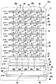
図4は、CCDイメージセンサ10aを概略的に示す部分平面図である。ただし、同図においては、図2に示した光遮蔽膜51、保護膜52、第1の平坦化膜53、第2の平坦化膜56およびマイクロレンズアレイ58の図示を省略している。また、色フィルタアレイ55自体の図示も省略しているが、各光電変換素子15上に配置されている色フィルタの色を記号G1、G2、RまたはBで示してある。記号G1、G2、RおよびBの意味は、図3におけるこれらの記号の意味と同じである。図4に示した構成要素のうちで図2において既に示した構成要素については、図2で用いた参照符号と同じ参照符号を付してある。
【0086】
図4に示すように、CCDイメージセンサ10aにおいては、半導体基板11に多数個の光電変換素子15が複数行、複数列に亘って行列状に配設されている。実際のCCD撮像システムでは、光電変換素子15の総数が例えば数100万個を超える。光電変換素子列方向および光電変換素子行方向の光電変換素子のピッチは、例えば2〜10μmの範囲内で適宜選定される。
【0087】
1列の光電変換素子列に1本ずつ、その右側(図4での右側)に沿って垂直電荷転送チャネル20aが近接配置されている。
【0088】
第1〜第2垂直転送電極25〜26は、1行の光電変換素子行に各々1本ずつ配設されている。第1垂直転送電極25の各々は、各垂直電荷転送チャネル20aと平面視上交差しつつ、対応する光電変換素子行に沿ってその下流側に延在する。第2垂直転送電極26の各々は、各垂直電荷転送チャネル20aと平面視上交差しつつ、対応する光電変換素子行に沿ってその上流側に延在する。
【0089】
各第1垂直転送電極25は、対応する光電変換素子15それぞれの図4での右側方において、1つの読出ゲート用チャネル領域21a(図2参照)と共に1つの読出ゲート21を構成する。図4に示したII−II線に沿った断面を拡大して概略的に示した図が、図2に相当する。
【0090】
1行の光電変換素子行に対応する第1〜第2垂直転送電極25〜26は、左端の光電変換素子列に含まれる光電変換素子15を除き、この光電変換素子行中の光電変換素子15の各々を平面視上取り囲んで光電変換素子領域16を画定している。
【0091】
最も下流の第1垂直転送電極25の下流側に、第1〜第3補助転送電極31〜33がこの順番で1本ずつ配設されている。これらの第1〜第3補助転送電極31〜33の各々も、各垂直電荷転送チャネル20aと平面視上交差しつつ、光電変換素子行方向に延在する。
【0092】
第1〜第2転送制御電極36〜37が、第3補助転送電極33の下流側にこの順番で配設されている。これら第1〜第2転送制御電極36〜37も、各垂直電荷転送チャネル20aと平面視上交差しつつ、光電変換素子行方向に延在する。
【0093】
第2垂直転送電極26、第1補助転送電極31、第3補助転送電極33および第2転送制御電極37は、半導体基板11上の第1レベルに設けられた第1ポリシリコン層によって形成される。第1垂直転送電極25、第2補助転送電極34および第1転送制御電極36は、半導体基板11上の第1レベルよりも上の第2レベルに設けられた第2ポリシリコン層によって形成される。個々の電極25〜26、31〜33および36〜37は、前述したように電気的絶縁膜(熱酸化膜)50(図2参照)によって覆われている。
【0094】
垂直電荷転送チャネル20aの各々において第1垂直転送電極25、第2垂直転送電極26、第1補助転送電極31、第2補助転送電極32、または第3補助転送電極33と対向する領域は、その上の電極25、26、31、32または33と共に1つの垂直電荷転送段を構成する。
【0095】
1本の垂直電荷転送チャネル20aを含んで構成される垂直電荷転送段の各々は、光電変換素子列方向に連なって1つの垂直電荷転送素子20を構成する。個々の垂直電荷転送チャネル20aのうちで垂直電荷転送素子20を構成する領域は、n型チャネルによって構成されている。
【0096】
一方、垂直電荷転送チャネル20aの各々において第1転送制御電極36および第2転送制御電極37と対向する領域は、その上の転送制御電極36、37と共に1つの電荷転送段35aを構成する。この電荷転送段35aを、以下、「転送制御段35a」という。
【0097】
これらの転送制御段35aは、全体として1つのCCDラインメモリ部35を構成する。CCDラインメモリ部35での垂直電荷転送チャネル20aの構成については、後に図6(A)を参照しつつ詳述する。
【0098】
各垂直電荷転送チャネル20aの下流端(第1電荷転送チャネル領域の下流端)は、水平電荷転送素子(HCCD)40に電気的に接続されている。
【0099】
水平電荷転送素子40に沿って、掃出ドレイン45が設けられている。この掃出ドレイン45とCCDラインメモリ部35とは、平面視上、水平電荷転送素子40を挟んで対向する。
【0100】
掃出ドレイン45は、半導体基板11のp型不純物添加領域11bに形成されたn型ドレイン領域46と、p型不純物添加領域11bによって構成された掃出ドレイン用チャネル領域と、掃出ドレイン用チャネル領域上に電気的絶縁膜を介して配置された掃出ゲート電極47bとを有する。掃出ドレイン45の構成については、後に図6(A)および図6(B)を参照しつつ詳述する。
【0101】
水平電荷転送素子40の一端に、出力部60が接続されている。この出力部60は、水平電荷転送素子40から送られてきた電荷を例えばフローティング容量(図示せず。)によって信号電圧に変換し、この信号電圧をソースホロワ回路(図示せず。)等を利用して増幅する。検出(変換)された後のフローティング容量の電荷は、図示を省略したリセットトランジスタを介して電源(図示せず。)に吸収される。出力部60は、例えば、特願平11−287326号明細書の第0084段〜0091段において図4(b)を参照しつつ説明されている出力部と同様にして構成することができる。
【0102】
以下、図5、図6(A)および図6(B)を参照しつつ、CCDラインメモリ部35、水平電荷転送素子40および掃出ドレイン45それぞれの構成について詳述する。
【0103】
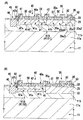
図5は、CCDラインメモリ部35から掃出ドレイン45にかけての領域を拡大して示す概略図である。
【0104】
図6(A)は、図5に示したVIA−VIA線に沿った断面の概略図であり、図6(B)は、図5に示したVIB−VIB線に沿った断面の概略図である。
【0105】
図5または図6(A)に示すように、垂直電荷転送チャネル20aそれぞれの下流端は、水平電荷転送チャネル41に接している。
【0106】
図6(A)に示すように、CCDラインメモリ部35での垂直電荷転送チャネル20aの各々は、n型不純物添加領域(n型チャネル)20a1の上にp- 型不純物添加領域20a2が形成されている1つのポテンシャル・バリア領域20aBと、n型不純物添加領域(n型チャネル)20a1のみによって構成されている1つのポテンシャル・ウェル領域20aWとを有する。
【0107】
ポテンシャル・バリア領域20aBの幅(光電変換素子列方向の幅)は、例えば0.5〜1μm程度であり、ポテンシャル・ウェル領域20aWの幅(光電変換素子列方向の幅)は、例えば2〜20μm程度である。いずれの領域20aB、20aWも、電荷転送チャネルとしての導電型はn型である。
【0108】
第1転送制御電極36は、ポテンシャル・バリア領域20aBの上方に電気的絶縁膜23を介して配置されている。第2転送制御電極37は、ポテンシャル・ウェル領域20aWの上方に電気的絶縁膜23を介して配置されている。例えば、第1ポリシリコン層によって第2転送制御電極37が形成され、第2ポリシリコン層によって第1転送制御電極36が形成される。
【0109】
個々の転送制御段35aは、1つのポテンシャル・バリア領域20aBと、その上方の第1転送制御電極36と、1つのポテンシャル・ウェル領域20aWと、その上方の第2転送制御電極37とによって構成される。
【0110】
第1転送制御電極36と第2転送制御電極37とは共通結線され、制御信号φLMの供給を受ける。制御信号φLMのレベルを制御してポテンシャル・バリア領域20aBの電位を高くすることにより、垂直電荷転送素子20から転送制御段35aへ電荷を転送することが可能になる。制御信号φLMのレベルを制御してポテンシャル・ウェル領域20aWの電位を低くすることにより、転送制御段35aから水平電荷転送素子40へ電荷を転送することができる。
【0111】
転送制御段35aから水平電荷転送素子40への電荷転送については、後に図9を参照しつつ詳述する。
【0112】
図5に示すように、水平電荷転送素子40は、光電変換素子行方向に帯状に延在する1本の水平電荷転送チャネル41と、この水平電荷転送チャネル41上に形成された多数個の第1〜第2水平転送電極42〜43とを有する。
【0113】
図6(A)および図6(B)に示すように、水平電荷転送チャネル41は、n型不純物添加領域(n型チャネル)41a上にp- 型不純物添加領域41bが形成されているポテンシャル・バリア領域41Bと、n型不純物添加領域(n型チャネル)41aのみによって構成されているポテンシャル・ウェル領域41Wとを有する。いずれの領域41B、41Wも、電荷転送チャネルとしての導電型はn型である。
【0114】
ポテンシャル・バリア領域41Bは、光電変換素子行方向に帯状に延在する1つの第1バリア領域41B1と、第1バリア領域41B1から一定の間隔で分岐して光電変換素子列方向に帯状に延在する多数の第2バリア領域41B2とを含む。1つの第2バリア領域41B2とその下流の第2バリア領域41B2との間に、これらに隣接する1つのポテンシャル・ウェル領域41Wが形成されている。最も下流の第2バリア領域41B2の下流側にも、1つのポテンシャル・ウェル領域41Wが形成されている。
【0115】
第1バリア領域41B1は、転送制御段35aと水平電荷転送素子40内のポテンシャル・ウェル領域41Wとを分離する。第2バリア領域41B2の各々は、水平電荷転送素子40内でポテンシャル・ウェル領域41W同士を分離する。
【0116】
個々の第1水平転送電極42は、1つの第2バリア領域41B2と、この第2バリア領域41B2に続く第1バリア領域41B1とを覆う。第1水平転送電極42は、平面視上、逆L字状を呈する(図5参照)。
【0117】
個々の第2水平転送電極43は、1つのポテンシャル・ウェル領域41Wを覆う。第2水平転送電極43は、平面視上、矩形を呈する(図5参照)。
【0118】
これらの第1および第2水平転送電極42、43は、電気的絶縁膜23を介して半導体基板1上に形成されている。例えば、第2ポリシリコン層によって第2水平転送電極43が形成され、第3ポリシリコン層によって第1水平転送電極42が形成される。
【0119】
1個の第1水平転送電極42と、その下方のポテンシャル・バリア領域41Bと、1個の第2水平転送電極43と、その下方のポテンシャル・ウェル領域41Wとは、1つの水平電荷転送段40aまたは補助水平電荷転送段40bを構成する。水平電荷転送段40aは、1本の垂直電荷転送チャネル20aに1つずつ対応しながら一列に形成されている。補助水平電荷転送段40bは、図5での最も左の垂直電荷転送チャネル20aに対応する水平電荷転送段40aの下流側(後述する出力部60側を意味する。)に、計3つ形成されている。
【0120】
1つの水平電荷転送段または補助水平電荷転送段を構成する第1および第2水平転送電極42、43は共通結線され、水平駆動信号φH1、φH2またはφH3の供給を受ける。
【0121】
転送制御段35aから水平電荷転送素子40へ電荷を転送する際には、制御信号φLMならびに水平駆動信号φH1、φH2またはφH3のレベルが例えば次のように制御される。すなわち、水平電荷転送段40aにおけるポテンシャル・バリア領域41Bの電位が、転送制御段35aにおけるポテンシャル・ウェル領域20aWの電位よりも相対的に高くなるように制御される。転送制御段35aから水平電荷転送素子40へ電荷を転送することが可能になる。転送制御段35aから水平電荷転送素子40への電荷転送の原理については、後に図9を参照しつつ詳述する。
【0122】
水平電荷転送素子40内で電荷を転送する際には、水平駆動信号φH1、φH2およびφH3のレベルが例えば次のように制御される。すなわち、電荷が分布している水平電荷転送段40aにおけるポテンシャル・ウェル領域41Wの電位が、その下流の水平電荷転送段40aにおけるポテンシャル・バリア領域41Bの電位よりも相対的に低くなるように制御される。
【0123】
図5、図6(A)または図6(B)に示すように、掃出ドレイン45は、光電変換素子行方向に延在するドレイン領域46を有する。このドレイン領域46は、例えば、半導体基板11のp型不純物添加領域11bに帯状に形成されたn+ 型不純物添加領域によって構成される。
【0124】
掃出ドレイン用チャネル領域47aが、ドレイン領域46と水平電荷転送チャネル41との間に介在する。この掃出ドレイン用チャネル領域47aは、例えばp型不純物添加領域11bの一部によって構成され、光電変換素子行方向に延在する。
【0125】
掃出ゲート電極47bが、掃出ドレイン用チャネル領域47aを平面視上覆う。この掃出ゲート電極47bは、例えば第1ポリシリコン層によって、電気的絶縁膜23上に形成される。掃出ドレイン用チャネル領域47aと掃出ゲート電極47bとは、掃出ゲート47を構成する。
【0126】
掃出ゲート電極47bは、制御信号φDRの供給を受ける。制御信号φDRの電圧を例えば15〜20V程度にすると、掃出ドレイン用チャネル領域47aの表面付近が反転する。水平電荷転送チャネル41とドレイン領域46とが導通する。水平電荷転送段内および補助水平電荷転送段内の電荷をドレイン領域46へ排出することができる。水平電荷転送素子40から掃出ドレイン45への電荷転送の原理については、後に図9を参照しつつ詳述する。
【0127】
なお、個々の水平転送電極42〜43および掃出ゲート電極47bは、それぞれが別個に、電気的絶縁膜(熱酸化膜)50(図6(A)または図6(B)参照)によって覆われている。図6(B)に示すように、各垂直電荷転送チャネル20aの平面視上の周囲には、水平電荷転送チャネル41との隣接箇所を除いて、チャネルストップ22が配置されている。
【0128】
以上説明した構成を有するCCDイメージセンサ10aは、駆動回路65(図1参照)から供給される駆動信号および制御信号に従って駆動する。
【0129】
図4には、垂直電荷転送素子20の各々を4相の垂直駆動信号φV1〜φV4によって駆動させる際の配線例を付記してある。図5には、水平電荷転送素子40を3相の水平駆動信号φH1〜φH3によって駆動させる際の配線例を付記してある。図4および図5には、CCDラインメモリ部35を制御信号φLMによって駆動させ、掃出ドレイン45を制御信号φDRによって駆動させる際の配線例も付記してある。
【0130】
図4に示すように、垂直電荷転送素子20の各々を4相駆動させるために、第1〜第2垂直転送電極25〜26の各々と第1〜第3補助転送電極31〜33とが4つのグループに分けられている。グループ毎に異なる垂直駆動信号φV1〜φV4が供給される。1つのグループは、3本おきに選択された第1垂直転送電極25、第2垂直転送電極26、第1補助転送電極31、第2補助転送電極34または第3補助転送電極33によって構成されている。
【0131】
図5に示すように、水平電荷転送素子40を3相駆動するために、最も下流の補助水平電荷転送段を基点にして各水平電荷転送段および各補助水平電荷転送段が3つのグループに分けられている。1つのグループは、2つおきに選択された水平電荷転送段および補助水平電荷転送段によって構成される。
【0132】
1つのグループに水平駆動信号φH1が供給され、他の1つのグループに水平駆動信号φH2が供給され、残りのグループに水平駆動信号φH3が供給される。図示の例では、最も下流の補助水平電荷転送段に水平駆動信号φH1が供給され、下流から2番目の補助水平電荷転送段に水平駆動信号φH2が供給される。最も上流の補助水平電荷転送段(下流から3番目の補助水平電荷転送段)には、水平駆動信号φH3が供給される。
【0133】
図4および図5に示すように、制御信号φLMは、第1〜第2転送制御電極36〜37の各々に供給される。制御信号φDRは、掃出ゲート電極47bに供給される。
【0134】
なお、本明細書においては、駆動信号を供給する電圧供給線に接続された後の水平電荷転送素子における水平転送電極の数を、以下の約束の下に数えるものとする。
【0135】
すなわち、互いに隣接し、かつ同一の電圧供給配線に接続されている複数個の水平転送電極は、これらをまとめて1個として数えるものとする。この約束の下では、互いに隣接してはいるが、互いに異なる電圧供給線に接続されている2個の水平転送電極の数は、2個である。また、同一の電圧供給配線に接続されてはいるが、互いに離隔している2個の水平転送電極の数も2個である。
【0136】
上記の約束事は、次の場合にも適用するものとする。すなわち、複数の第1電荷転送チャネル領域(例えば、複数本の垂直電荷転送チャネル20aそれぞれにおける下流側端部)と、これらの第1電荷転送チャネル領域の各々に電気的に接続される第2電荷転送チャネルを含む電荷転送素子(例えば水平電荷転送素子40)とを備えた電荷転送装置であって、第2電荷転送チャネル上に電気的絶縁膜を介して形成された複数個の転送電極を有し、これらの転送電極の各々が所定の電圧供給配線に接続されている電荷転送装置における転送電極の数を数える際にも適用するものとする。また、CCDラインメモリ部における転送制御電極の数を数える際にも適用するものとする。
【0137】
上記の約束事に従えば、図5に示した水平電荷転送素子40は、1水平電荷転送段40a当たり、および1補助水平電荷転送段40b当たり、1個の水平転送電極を有する。水平電荷転送素子40は、光電変換素子行方向に連続する3個の水平転送電極を1群とする複数群の水平転送電極を有する。1つの群を構成する3個の水平転送電極の各々は、互いに異なる電圧供給線に接続されている。3個を周期とする水平転送電極の各々は、同一の電圧供給線に接続されている。
【0138】
CCD撮像システム100(図1参照)においては、撮像モードが静止画記録モードであるかモニターモードであるかに応じて、所定波形の駆動信号φV1〜φV4、制御信号φLMおよびφH1〜φH3が駆動回路65からCCDイメージセンサ10に供給される。垂直電荷転送素子20の各々、CCDラインメモリ部35および水平電荷転送素子40は、CCD撮像システム100の撮像モードに応じた所定の動作を行う。
【0139】
以下、CCD撮像システム100の撮像モードがモニターモードのときの各垂直電荷転送素子20、CCDラインメモリ部35、水平電荷転送素子40および掃出ドレイン45の動作の一例について説明する。
【0140】
CCD撮像システム100の撮像モードがモニターモードのときには、例えば1/2間引き走査の下に各垂直電荷転送素子20が駆動される。また、不要電荷が、CCDラインメモリ部35から水平電荷転送素子40を介して掃出ドレイン45へ排出される。
【0141】
各垂直電荷転送素子20を1/2間引き走査の下に駆動させる場合、1つの垂直期間に全光電変換素子行のうちの1/2の光電変換素子行、例えば1行おきの光電変換素子行を対象に、光電変換素子15から各垂直電荷転送素子20へ電荷が読み出される。このとき、垂直駆動信号φV1およびφV3のいずれかに読出パルスが重畳される。
【0142】
垂直電荷転送素子20の各々に読み出された電荷は、垂直電荷転送素子内を順次転送されて、CCDラインメモリ部35を構成する転送制御段に達する。1つの光電変換素子行中の光電変換素子15の各々から各垂直電荷転送素子20へ読み出された電荷は、同じタイミングで転送制御段に達する。
【0143】
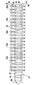
図7に示すように、モニターモードの際には、各垂直電荷転送チャネル20aが2つのグループ、すなわち、必要電荷を転送する第1グループGp1と不要電荷を転送する第2グループGp2とに分けられる。第1グループGp1は、水平駆動信号φH1が供給される水平電荷転送段に対応する垂直電荷転送チャネル20aの各々によって構成される。第2グループGp2は、水平駆動信号φH2、φH3が供給される水平電荷転送段に対応する垂直電荷転送チャネル20aの各々によって構成される。
【0144】
なお、図7に示した構成要素は全て図5に示されているので、各構成要素には図5で用いた参照符号と同じ参照符号を付してその説明を省略する。
【0145】
以下、不要電荷を水平電荷転送素子40を介して掃出ドレイン45へ排出した後に必要電荷を水平電荷転送素子40へ転送し、更にこれらの必要電荷を出力部60へ向けて転送する方法について、図8、図9、図10(A)および図10(B)を参照しつつ説明する。
【0146】
下記の説明においては、個々の垂直電荷転送チャネル20aを介して転送される電荷を、この垂直電荷転送チャネル20aに対応する光電変換素子15の上方に配置されている色フィルタの色に応じて、「電荷g1」、「電荷r」、「電荷g2」、「電荷b」と称する。第1グループGp1を構成する垂直電荷転送チャネル20aの各々は、電荷g1または電荷bを転送する。第2グループGp2を構成する垂直電荷転送チャネル20aの各々は、電荷rまたは電荷g2を転送する。
【0147】
図8は、必要電荷だけをCCDラインメモリ部35から出力部60へ転送する場合の制御信号φLM、水平駆動信号φH1〜φH3および制御信号φDRの波形の一例を示す。
【0148】
図9は、CCDラインメモリ部35から水平電荷転送素子40へ、また、CCDラインメモリ部35から水平電荷転送素子40を介して掃出ドレイン45へ電荷を転送する際の原理を模式的に示す。
【0149】
図10(A)は図8に示した時刻t1での電荷の分布の様子を模式的に示し、図10(B)は図8に示した時刻t2での電荷の分布の様子を模式的に示す。
【0150】
なお、図9、図10(A)、図10(B)に示した構成要素は全て図6(A)または図7に示されているので、各構成要素には図6(A)または図7で用いた参照符号と同じ参照符号を付してその説明を省略する。
【0151】
図8に示すように、CCDラインメモリ部35から水平電荷転送素子40へ電荷を転送する前の段階の時刻t0では、水平駆動信号φH1〜φH3がローレベルL(例えば0V)にあり、制御信号φLMがハイレベルH(例えば+3.3V)にある。
【0152】
図9に示すように、水平駆動信号φHn(nは1〜8のうちの任意の整数を表す。以下同じ。)がローレベルLのとき、第1水平転送電極42下の水平電荷転送チャネル46(ポテンシャル・バリア領域41B)の電位は、制御信号φLMがハイレベルHにあるかローレベルLにあるかに拘わらず、第2転送制御電極37下の垂直電荷転送チャネル20a(ポテンシャル・ウェル領域20aW)の電位より低い。したがって、水平駆動信号φHnがローレベルLにあると、図9に記号○で示した電荷はCCDラインメモリ部35から水平電荷転送素子40へ転送されることなく、CCDラインメモリ部35に留まる。
【0153】
したがって、図8に示した時刻t0においては、CCDラインメモリ部35から水平電荷転送素子40へ電荷が転送されない。
【0154】
図8に示した時刻t1におけるように、CCDラインメモリ部35から水平電荷転送素子40へ不要電荷を転送する際には、制御信号φLMをハイレベルHからローレベルL(例えば0V)にする。水平駆動信号φH1をローレベルLにし、水平駆動信号φH2〜φH3をハイレベルHにする。さらに、制御信号φDRをハイレベルH(例えば15〜20V)にする。
【0155】
図9に示すように、水平駆動信号φHnがハイレベルHにあり、かつ、制御信号φLMがローレベルLにあると、第1水平転送電極42下での水平電荷転送チャネル46(ポテンシャル・バリア領域41B)の電位が第2転送制御電極37下の垂直電荷転送チャネル20a(ポテンシャル・ウェル領域20aW)の電位より高くなる。したがって、電荷○がCCDラインメモリ部35から水平電荷転送素子40へ転送される。
【0156】
このとき、制御信号φDRがローレベルL(例えば5V)であると、掃出ゲート用チャネル領域47aは反転しない。掃出ゲート用チャネル領域47aの電位は、第2水平転送電極43下の水平電荷転送チャネル41(ポテンシャル・ウェル領域41W)の電位より低い。水平電荷転送段40aとドレイン領域46とは導通しない。水平電荷転送素子40に転送された電荷○は、ドレイン領域46へ排出されることなく、水平電荷転送素子40に留まる。
【0157】
一方、制御信号φDRがハイレベルHであると、掃出ゲート用チャネル領域47aの表面付近が反転する。掃出ゲート用チャネル領域47aの電位が、第2水平転送電極43下の水平電荷転送チャネル41(ポテンシャル・ウェル領域41W)の電位より高くなる。水平電荷転送段40aとドレイン領域46とが導通する。水平電荷転送素子40内の電荷○が、掃出ドレイン45(ドレイン領域46)へ排出される。
【0158】
したがって、図8に示した時刻t1では、水平駆動信号φH2またはφH3が供給されている水平電荷転送段の各々へCCDラインメモリ部35から電荷が転送され、さらに、これらの電荷が掃出ドレイン45へ排出される。
【0159】
図10(A)は、図8に示した時刻t1での各電荷g1、r、g2およびbの分布状態を示す。水平駆動信号φH2、φH3が供給されている水平電荷転送段の各々へ、第2グループGp2の垂直電荷転送チャネル20aの各々から不要電荷r、g2が転送され、更に、これらの不要電荷r、g2が掃出ドレイン45へ排出されている。同図においては、各不要電荷の移動経路を矢印で示している。
【0160】
水平駆動信号φH1が供給されている水平電荷転送段の各々へは、CCDラインメモリ部35から電荷が転送されない。すなわち、第1グループGp1の垂直電荷転送チャネル20aの各々から水平電荷転送素子40へは、必要電荷が転送されない。
【0161】
次いで、水平駆動信号φH2およびφH3をハイレベルHからローレベルLにする。続いて、制御信号φLMをローレベルLからハイレベルHにし、CCDラインメモリ部35から水平電荷転送素子40への電荷の転送を禁止する。
【0162】
その後、制御信号φDRをハイレベルHに維持したまま、水平駆動信号φH3、φH2およびφH1をこの順番で順次ローレベルLからハイレベルHにする。水平駆動信号φH2がハイレベルHにある間に、水平駆動信号φH3をハイレベルHからローレベルLに戻す。水平駆動信号φH1がハイレベルHにある間に、水平駆動信号φH2をハイレベルHからローレベルLに戻す。水平駆動信号φH1は、一定時間経過後にローレベルLに戻す。この動作は、水平電荷転送素子40内の電荷をそれぞれ1水平電荷転送段分、下流側に転送する動作に相当する。
【0163】
この転送動作により、掃出ドレイン45への不要電荷の排出を十分に行うことができない水平電荷転送段が仮にあったとしても、この水平電荷転送段以外の水平電荷転送段において不要電荷を掃出ドレイン45へ排出することができる。不要電荷を高い確率で掃出ドレイン45へ排出することができる。
【0164】
水平駆動信号φH1をハイレベルHからローレベルLへ戻した後に、制御信号φLMをハイレベルHからローレベルLにする。さらに、制御信号φDをハイレベルHからローレベルLにし、水平電荷転送素子40から掃出ドレイン45への電荷の排出を禁止する。
【0165】
その後、図8の時刻t2におけるように、水平駆動信号φH1のみを再びハイレベルにする。制御信号φLMはローレベルLにあり、制御信号φDRもローレベルLにある。したがって、水平駆動信号φH1が供給されている水平電荷転送段の各々に、ラインメモリ35から電荷が転送される。
【0166】
図10(B)は、図8に示した時刻t2での各電荷g1、r、g2およびbの分布状態を示す。水平駆動信号φH1が供給されている水平電荷転送段の各々へ、第1グループGp1の垂直電荷転送チャネル20aの各々から必要電荷g1、r、g2またはbが転送されている。これらの必要電荷は、掃出ドレイン領域45へは排出されずに、水平電荷転素子40内に留まる。
【0167】
この後、水平駆動信号φH1をハイレベルHからローレベルLにしてから制御信号φLMをローレベルLからハイレベルHにし、CCDラインメモリ部35から水平電荷転送素子40への電荷の転送を禁止する。引き続き、水平駆動信号φH3、φH2およびφH1をこの順番でローレベルLからハイレベルHへと、また、ハイレベルHからローレベルLへと、繰返し変化させる。
【0168】
その結果、水平電荷転送素子40内の電荷g1、b、g2、rの各々が、出力部60へ向けて1水平電荷転送段または1補助水平電荷転送段ずつ、順次転送される。
【0169】
以上のようにラインメモリ部35、水平電荷転送素子40および掃出ドレイン45を制御することにより、各垂直電荷転送素子20に読み出された電荷の中から不要電荷を掃出ドレイン45へ排出して、必要電荷だけを水平電荷転送素子45によって出力部60へ転送することができる。1/3に間引かれた電荷が、水平電荷転送素子45から出力部60へ転送される。
【0170】
出力部60は、水平電荷転送素子40から受け取った電荷(必要電荷)に基づいて、画像信号(信号電圧)を順次出力する。図1に示した映像信号処理回路70は、これらの画像信号(信号電圧)を利用して画像データを生成する。映像信号処理回路70で生成された画像データは、画像データ出力部75へ送られて、フレームメモリ等の記憶媒体に一旦記憶される。その後、画像データ出力部75から表示部80へ画像データが供給され、表示部80が画像を表示する。
【0171】
第1の実施例によるCCDイメージセンサ10aを備えたCCD撮像システム100は、上述のようにして不要電荷を掃出ドレイン45へ排出して、必要電荷のみに基づいて画像信号を生成することができる。
【0172】
したがって、光電変換素子列方向および光電変換素子行方向のいずれについても所望の電荷を間引いて、垂直画素数および水平画素数の両方が間引かれた画像データを生成することが容易である。垂直画素数のみを間引いた画素データに基づいてモニター表示する場合に比べて、良好なモニター画像を得ることが容易になる。動画をモニター表示することもできるし、静止画をモニター表示することも可能である。勿論、光電変換素子行方向についてのみ所望の電荷を間引いて、水平画素数のみが間引かれた画像データを生成することも可能である。
【0173】
水平電荷転送素子40から出力部60へ転送する電荷の数が1/3に減ることから、次の利点が得られる。
【0174】
すなわち、全ての垂直電荷転送素子から電荷を受け取り、これらの電荷を全て出力部へ転送していた従来の水平電荷転送素子に比べて、同じデータレートの下での1水平読出期間の長さがほぼ1/3に短縮される。これに伴って、モニター表示の際のフレーム周波数をほぼ3倍に高めることができ、より自然なモニター表示を行うことが容易になる。従来と同じフレーム周波数でモニター表示を行った場合には、データレートがほぼ1/3になることから、水平電荷転送素子の駆動周波数をほぼ1/3に低減させることができる。その結果、CCD撮像システムにおける主な電力消費源である水平電荷転送素子の駆動電力をほぼ1/3に削減することができる。
【0175】
一方、CCD撮像システム100の撮像モードが静止画記録モードのときには、例えばインターレース走査の下に各垂直電荷転送素子20が駆動される。1つの光電変換素子行から各垂直電荷転送素子20へ読み出された電荷の各々は、同じタイミングでCCDラインメモリ部35まで転送される。電荷の垂直加算は行われない。
【0176】
静止画記録モードの際には、各垂直電荷転送チャネル20aが第1〜第3グループの計3つのグループに分けられる。そして、これら第1〜第3グループ毎に異なるタイミングで、CCDラインメモリ部35から水平電荷転送素子40へ電荷が転送される。1つのグループは、2本おきに選択された垂直電荷転送チャネル20aの各々によって構成される。
【0177】
まず、1つのグループの各垂直電荷転送チャネル20aから、例えば水平駆動信号φH1が供給されている水平電荷転送段の各々へ電荷が転送される。これらの電荷を水平電荷転送素子40から出力部60へ転送し終えた後に、他の1つのグループの各垂直電荷転送チャネル20aから、例えば水平駆動信号φH2が供給されている水平電荷転送段の各々へ電荷が転送される。これらの電荷を水平電荷転送素子40から出力部60へ転送し終えた後に、最後の1つのグループの各垂直電荷転送チャネル20aから、例えば水平駆動信号φH3が供給されている水平電荷転送段の各々へ電荷が転送され、さらに、出力部60へ転送される。水平電荷転送素子40から掃出ドレイン45への電荷の排出は、行われない。
【0178】
CCDラインメモリ部35から水平電荷転送素子40(水平電荷転送段)への電荷の転送は、図9を用いて既に説明した原理に従って行われる。
【0179】
水平電荷転送素子40内での電荷転送の際には、水平駆動信号φH1〜φH3が所定の順番および位相の下にローレベルLからハイレベルHへ、また、ハイレベルHからローレベルLへと繰返しそのレベルを変化させる。
【0180】
出力部60は、水平電荷転送素子40から受け取った電荷に基づいて、画像信号(信号電圧)を順次出力する。図1に示した映像信号処理回路70は、これらの画像信号(信号電圧)を利用して静止画の画像データを生成する。映像信号処理回路70で生成された画像データは、画像データ出力部75へ送られて、フレームメモリ等の記憶媒体に一旦記憶される。
【0181】
その後、画像データ出力部75から表示部80へ画像データが供給され、表示部80が静止画を表示する。あるいは、画像データ出力部75から記録部82へ画像データが供給され、例えばメモリカード等の記録媒体に静止画の画像データが記録される。CCD撮像システム100は、全ての光電変換素子15それぞれに蓄積された電荷に基づいて、静止画の画像データを生成する。
【0182】
勿論、静止画記録モードの際に、光電変換素子列方向および光電変換素子行方向のいずれか一方または両方について所望の電荷を間引いて、垂直画素数および水平画素数のいずれか一方または両方が間引かれた画像データを生成することも可能である。
【0183】
水平電荷転送素子40をφH1〜φH6の6相の水平駆動信号によって駆動させると、各垂直電荷転送チャネル20aを2つのグループに分け、グループ毎に異なるタイミングで、水平電荷転送素子40へ電荷を転送することができる。個々のグループは、例えば、1本おきに選択された垂直電荷転送チャネル20aによって構成される。
【0184】
水平電荷転送素子40を4相の水平駆動信号φH1〜φH4によって駆動させると、光電変換素子行方向の電荷を1/2に間引いて出力部60へ転送することが可能になる。
【0185】
図11は、光電変換素子行方向の電荷を1/2に間引いて出力部60へ転送することを可能にする4相の水平駆動信号φH1〜φH4を水平電荷転送素子40へ供給するための配線例を示す。同図には、CCDラインメモリ部35へ制御信号φLMを供給し、掃出ドレイン45へ制御信号φDRを共有するための配線も付記してある。
【0186】
水平駆動信号φH1は、図11での最も左端の垂直電荷転送チャネル20aに対応する水平電荷転送段と、この水平電荷転送段の右側に7おきに選択された水平電荷転送段の各々、ならびに、左から3番目の垂直電荷転送チャネル20aに対応する水平電荷転送段と、この水平電荷転送段の右側に7おきに選択された水平電荷転送段の各々に供給される。
【0187】
水平駆動信号φH2は、左から2番目の垂直電荷転送チャネル20aに対応する水平電荷転送段と、この水平電荷転送段の右側に7おきに選択された水平電荷転送段の各々、ならびに、左から4番目の垂直電荷転送チャネル20aに対応する水平電荷転送段と、この水平電荷転送段の右側に7おきに選択された水平電荷転送段の各々に供給される。
【0188】
水平駆動信号φH3は、左から5番目の垂直電荷転送チャネル20aに対応する水平電荷転送段と、この水平電荷転送段の右側に7おきに選択された水平電荷転送段の各々、ならびに、左から7番目の垂直電荷転送チャネル20aに対応する水平電荷転送段と、この水平電荷転送段の右側に7おきに選択された水平電荷転送段の各々に供給される。
【0189】
水平駆動信号φH4は、左から6番目の垂直電荷転送チャネル20aに対応する水平電荷転送段と、この水平電荷転送段の右側に7おきに選択された水平電荷転送段の各々、ならびに、左から8番目の垂直電荷転送チャネル20aに対応する水平電荷転送段と、この水平電荷転送段の右側に7おきに選択された水平電荷転送段の各々に供給される。
【0190】
図示の例では、水平駆動信号φH1が供給される水平電荷転送段の各々に対応する各垂直電荷転送チャネル20aが、第1グループGp1を構成する。水平駆動信号φH2が供給される水平電荷転送段の各々に対応する各垂直電荷転送チャネル20aが、第2グループGp2を構成する。水平駆動信号φH3、φH4が供給される水平電荷転送段の各々に対応する各垂直電荷転送チャネル20aが、第3グループGp2を構成する。
【0191】
第1および第2グループGp1、Gp2の垂直電荷転送チャネル20aは、それぞれ必要電荷を転送する。第3グループGp3の垂直電荷転送チャネル20aは、不要電荷を転送する。
【0192】
図12は、不要電荷を掃出ドレイン45へ排出した後、必要電荷を出力部60へ転送する場合の制御信号φLM、水平駆動信号φH1〜φH4および制御信号φDRの波形の一例を示す。
【0193】
図13(A)、図13(B)、図14は、図12に示した時刻T1、T2またはT3での電荷の分布の様子を模式的に示す。
【0194】
図12に示すように、CCDラインメモリ部35から水平電荷転送素子40へ電荷を転送する前の段階の時刻T0では、水平駆動信号φH2、φH4および制御信号φDRがそれぞれローレベルLにあり、水平駆動信号φH1、φH3および制御信号φLMがそれぞれハイレベルHにある。
【0195】
制御信号φLMがハイレベルHにあることから、CCDラインメモリ部35から水平電荷転送素子40への電荷の転送が禁止される。
【0196】
図12に示した時刻T1におけるように、CCDラインメモリ部35から水平電荷転送素子40へ不要電荷を転送する際には、制御信号φLMをハイレベルHからローレベルLにする。水平駆動信号φH1、φH2をローレベルLにし、水平駆動信号φH3、φH4をハイレベルHにする。さらに、制御信号φDRをハイレベルHにする。
【0197】
制御信号φLMがローレベルLにあり、水平駆動信号φH1〜φH4のうちのφH3およびφH4がハイレベルHにあることから、水平駆動信号φH3またはφH4が供給されている水平電荷転送段の各々へCCDラインメモリ部35から電荷が転送される。すなわち、第3グループGp3の垂直電荷転送チャネル20aの各々から水平電荷転送素子40へ不要電荷が転送される。
【0198】
水平電荷転送素子40へ転送された不要電荷は、制御信号φDRがハイレベルHにあることから、水平電荷転送素子40から掃出ドレイン45へ排出される。
【0199】
図13(A)は、図12に示した時刻T1での各電荷g1、r、g2およびbの分布状態を示す。水平駆動信号φH3、φH4が供給されている水平電荷転送段の各々へ、第3グループGp3の垂直電荷転送チャネル20aの各々から不要電荷g1、r、g2、bが転送され、更に、これらの不要電荷g1、r、g2、bが掃出ドレイン45へ排出されている。同図においては、各不要電荷の移動経路を矢印で示している。
【0200】
水平駆動信号φH1、φH2が供給されている水平電荷転送段の各々へは、CCDラインメモリ部35から電荷が転送されない。すなわち、第1および第2グループGp1、Gp2の垂直電荷転送チャネル20aの各々から水平電荷転送素子40へは、必要電荷が転送されない。
【0201】
次に、水平駆動信号φH3およびφH4をハイレベルHからローレベルLにする。続いて、制御信号φDRをハイレベルHからローレベルLにし、水平電荷転送素子40から掃出ドレイン45への電荷の排出を禁止する。制御信号φDRがローレベルLに転じるのに同期させて、または、やや遅れて、水平駆動信号φH1をローレベルLからハイレベルHにする。
【0202】
図12の時刻T2におけるように、水平駆動信号φH1のみがハイレベルHになり、他の水平駆動信号φH2〜φH3および制御信号φLM、φDRがローレベルLになる。水平駆動信号φH1が供給される水平電荷転送段に対応する垂直電荷転送チャネル20aの各々から水平電荷転送素子40へ、電荷が転送される。すなわち、第1グループGp1の垂直電荷転送チャネル20aの各々から水平電荷転送素子40へ必要電荷が転送される。
【0203】
図13(B)は、図12に示した時刻T2での各電荷g1、r、g2およびbの分布状態を示す。水平駆動信号φH1が供給されている水平電荷転送段の各々へ、第1グループGp1の垂直電荷転送チャネル20aの各々から必要電荷g1またはg2が転送されている。これらの必要電荷g1、g2は、掃出ドレイン45へ排出されることなく水平電荷転送素子40に留まる。同図においては、各必要電荷g1、g2の移動経路を矢印で示している。
【0204】
水平駆動信号φH2が供給されている水平電荷転送段の各々へは、CCDラインメモリ部35から電荷が転送されない。すなわち、第2グループGp2の垂直電荷転送チャネル20aの各々から水平電荷転送素子40へは、必要電荷が転送されない。
【0205】
この後、制御信号φLMをローレベルLからハイレベルHにし、CCDラインメモリ部35から水平電荷転送素子40への電荷の転送を禁止する。また、水平駆動信号φH4をハイレベルHにし、水平駆動信号φH1をローレベルLにする。水平駆動信号φH2をハイレベルHにする。水平駆動信号φH3は、ローレベルLにある。水平駆動信号φH1が供給される水平電荷転送段に分布していた必要電荷g1またはg2が、それぞれ1水平電荷転送段分下流側に転送される。
【0206】
次いで、水平駆動信号φH1をハイレベルHにし、水平駆動信号φH2をローレベルLにする。水平駆動信号φH3をハイレベルHにし、水平駆動信号φH4をローレベルLにする。水平駆動信号φH2、φH4が供給される水平電荷転送段に分布していた必要電荷g1またはg2が、それぞれ1水平電荷転送段分下流側に転送される。
【0207】
さらに、水平駆動信号φH4をハイレベルHにし、水平駆動信号φH1をローレベルLにする。水平駆動信号φH2をハイレベルHにし、水平駆動信号φH3をローレベルLにする。水平駆動信号φH1、φH3が供給される水平電荷転送段に分布していた必要電荷g1またはg2が、それぞれ1水平電荷転送段分下流側に転送される。
【0208】
この後、図12の時刻T3におけるように、制御信号φLMをハイレベルHからローレベルLにする。このとき、制御信号φDRはローレベルLにあり、水平電荷転送素子40から掃出ドレイン45への電荷の排出を禁止している。水平駆動信号φH2はハイレベルHにあり、他の水平駆動信号φH1、φH3、φH4はローレベルLにある。水平駆動信号φH2が供給される水平電荷転送段に対応する垂直電荷転送チャネル20aの各々から水平電荷転送素子40へ、電荷が転送される。すなわち、第2グループGp2の垂直電荷転送チャネル20aの各々から水平電荷転送素子40へ必要電荷が転送される。
【0209】
図14は、図12に示した時刻T3での各電荷g1、r、g2およびbの分布状態を示す。水平駆動信号φH2が供給されている水平電荷転送段の各々へ、第2グループGp1の垂直電荷転送チャネル20aの各々から必要電荷rまたはbが転送されている。これらの必要電荷r、bは、掃出ドレイン45へ排出されることなく水平電荷転送素子40に留まる。同図においては、各必要電荷r、bの移動経路を矢印で示している。
【0210】
この段階で、水平電荷転送素子40には、必要電荷が最下流の補助水平電荷転送段から1補助水平電荷転送段または1水平電荷転送段おきに分布する。必要電荷g1、g2、r、bが下流側からこの順番で繰返し分布する。
【0211】
この後、制御信号φLMをローレベルLからハイレベルHにし、CCDラインメモリ部35から水平電荷転送素子40への電荷の転送を禁止する。引き続き、水平駆動信号φH1とφH3とを1組とし、水平駆動信号φH2とφH4とを他の1組として、各組の水平駆動信号をローレベルLからハイレベルHへと、また、ハイレベルHからローレベルLへと繰返し変化させる。このとき、一方の組の水平駆動信号の位相を、他方の組の水平駆動信号の位相から180°ずらす。水平駆動信号φH1を含む組を、最初にローレベルLにする。
【0212】
その結果、水平電荷転送素子40内の必要電荷g1、b、g2、rの各々が、出力部60へ向けて1水平電荷転送段または1補助水平電荷転送段ずつ、順次転送される。
【0213】
このようにしてラインメモリ部35、水平電荷転送素子40および掃出ドレイン45を制御することにより、水平電荷転送素子45から出力部60へ転送する電荷を1行の光電変換素子行当たり1/2に間引くことができる。
【0214】
この場合でも、水平電荷転送素子40を3相の水平駆動信号によって駆動させる場合と同様に、光電変換素子列方向についても所望の電荷を間引くことができる。垂直画素数および水平画素数のいずれか一方または両方が間引かれた画像信号を容易に生成することができる。
【0215】
したがって、垂直画素数および水平画素数の両方が間引かれた画像データを生成することが容易になる。垂直画素数のみを間引いた画素データに基づいてモニター表示する場合に比べて、良好なモニター画像を得ることが容易になる。動画をモニター表示することもできるし、静止画をモニター表示することも可能である。
【0216】
また、水平電荷転送素子40を3相の水平駆動信号によって駆動させた場合と同様の理由から、モニター表示の際のフレーム周波数を従来のほぼ2倍に高めることができ、より自然なモニター表示を行うことが容易になる。従来と同じフレーム周波数でモニター表示を行った場合には、データレートがほぼ1/2になることから、水平電荷転送素子の駆動周波数をほぼ1/2に低減させることができる。その結果、CCD撮像システムにおける主な電力消費源である水平電荷転送素子の駆動電力をほぼ1/2に削減することができる。
【0217】
一方、CCD撮像システム100の撮像モードが静止画記録モードのときには、例えばインターレース走査の下に各垂直電荷転送素子20が駆動される。1つの光電変換素子行から各垂直電荷転送素子20へ読み出された電荷の各々は、同じタイミングでCCDラインメモリ部35まで転送される。
【0218】
静止画記録モードの際にも、各垂直電荷転送チャネル20aが第1〜第2グループの計2つのグループに分けられる。そして、これら第1〜第2グループ毎に異なるタイミングで、CCDラインメモリ部35から水平電荷転送素子40へ電荷が転送される。1つのグループは、1本おきに選択された垂直電荷転送チャネル20aの各々によって構成される。
【0219】
まず、1つのグループ、例えば第1グループの各垂直電荷転送チャネル20aから水平電荷転送素子40へ電荷が転送される。これらの電荷を水平電荷転送素子40から出力部60へ転送し終えた後に、第2グループの各垂直電荷転送チャネル20aから水平電荷転送素子40へ電荷が転送され、さらに、出力部60へ転送される。
【0220】
CCDラインメモリ部35から水平電荷転送素子40への電荷の転送は、図9を用いて既に説明した原理に従って行われる。
【0221】
水平電荷転送素子40内での電荷転送の際には、水平駆動信号φH1〜φH4が所定の順番および位相の下にローレベルLからハイレベルHへ、また、ハイレベルHからローレベルLへと繰返しそのレベルを変化させる。
【0222】
出力部60は、水平電荷転送素子40から受け取った電荷に基づいて、画像信号(信号電圧)を順次出力する。図1に示した映像信号処理回路70は、これらの画像信号(信号電圧)を利用して静止画の画像データを生成する。映像信号処理回路70で生成された画像データは、画像データ出力部75へ送られて、フレームメモリ等の記憶媒体に一旦記憶される。
【0223】
その後、画像データ出力部75から表示部80へ画像データが供給され、表示部80が静止画を表示する。あるいは、画像データ出力部75から記録部82へ画像データが供給され、例えばメモリカード等の記録媒体に静止画の画像データが記録される。CCD撮像システム100は、全ての光電変換素子15それぞれに蓄積された電荷に基づいて、静止画の画像データを生成する。
【0224】
勿論、静止画記録モードの際に、光電変換素子列方向および光電変換素子行方向のいずれか一方または両方について所望の電荷を間引いて、垂直画素数および水平画素数のいずれか一方または両方が間引かれた画像データを生成することも可能である。
【0225】
次に、図1に示したCCDイメージセンサ10に係る第2の実施例によるCCDイメージセンサについて説明する。
【0226】
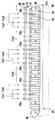
図15は、第2の実施例によるCCDイメージセンサ10bにおける光電変換素子、垂直電荷転送素子、CCDラインメモリ部、水平電荷転送素子、掃出ドレインおよび出力部の平面配置を概略的に示す部分平面図である。
【0227】
図15に示すように、CCDイメージセンサ10bにおいては、多数個の光電変換素子15が画素ずらし配置されている。この点で、CCDイメージセンサ10bは、第1の実施例によるCCDイメージセンサ10aと大きく異なる。
【0228】
他に下記(1) 〜(7) の点でも、CCDイメージセンサ10bはCCDイメージセンサ10aと異なる。
(1) 各光電変換素子15の平面視上の形状および各光電変換素子領域16の平面視上の形状が、それぞれ八角形である。
(2) 個々の垂直電荷転送チャネル20aが、対応する光電変換素子列に沿って蛇行する領域を含んでいる。これに伴って、個々の垂直電荷転送素子20も、対応する光電変換素子列に沿って蛇行する領域を含んでいる。
(3) 個々の光電変換素子15の平面視上の右斜下の辺に沿って、読出ゲート用チャネル領域が1つずつ配置されている。
(4) 最も下流の第1垂直転送電極25aを除き、第1垂直転送電極25aの各々が、水平電荷転送素子40側から数えて偶数番目の光電変換素子行とその直ぐ下流の奇数番目の光電変換素子行との間をこれらの光電変換素子行に沿って蛇行する領域を含んでいる。最も下流の第1垂直転送電極25aは、水平電荷転送素子40側から数えて1番目の光電変換素子行の下流側をこの光電変換素子行に沿って蛇行する領域を含んでいる。
(5) 最も上流の第2垂直転送電極26aを除き、第2垂直転送電極26aの各々が、水平電荷転送素子40側から数えて奇数番目の光電変換素子行とその直ぐ下流の偶数番目の光電変換素子行との間をこれらの光電変換素子行に沿って蛇行する領域を含んでいる。最も上流の第2垂直転送電極26aは、最も上流の光電変換素子行の上流側をこの光電変換素子行に沿って蛇行する領域を含んでいる。
(6) 個々の第1垂直転送電極25aは、この第1垂直転送電極25aが対応している奇数行中の光電変換素子それぞれに対応する全ての読出ゲート21を構成し、個々の第2垂直転送電極26aは、この第2垂直転送電極26aが対応している奇数行中の光電変換素子それぞれに対応する全ての読出ゲート21を構成する。
(7) 第1補助転送電極31が、蛇行しつつ全体としては光電変換素子行方向に延在している。
【0229】
これらの相違点を除けば、図15に示したCCDイメージセンサ10bは、第1の実施例によるCCDイメージセンサ10aと同様の構成を有する。
【0230】
このため、図15に示した構成要素のうちで図4に示した構成要素と機能上共通するものについては、図4で用いた参照符号と同じ参照符号を付してその説明を省略する。ただし、第1垂直転送電極については新たな参照符号「25a」を付し、第2垂直転送電極については新たな参照符号「26a」を付してある。
【0231】
なお、図15においては、光遮蔽膜、保護膜、第1の平坦化膜、第2の平坦化膜およびマイクロレンズアレイの図示を省略している。また、色フィルタアレイ自体の図示も省略しているが、各光電変換素子15上に配置されている色フィルタの色を記号G1、G2、RまたはBで示してある。記号G1、G2、RおよびBの意味は、図4におけるこれらの記号の意味と同様である。
【0232】
本実施例によるCCDイメージセンサ10bの特徴の1つである「画素ずらし配置」とは、本明細書においては下記の配置を意味する。
【0233】
すなわち、奇数番目に当たる光電変換素子列の各光電変換素子に対し、偶数番目に当たる光電変換素子列の光電変換素子の各々が、光電変換素子列内での光電変換素子のピッチの約1/2、列方向にずれ、奇数番目に当たる光電変換素子行の各光電変換素子に対し、偶数番目に当たる光電変換素子行の光電変換素子の各々が、光電変換素子行内での光電変換素子のピッチの約1/2、行方向にずれ、光電変換素子列の各々が奇数行または偶数行の光電変換素子のみを含むような、多数個の光電変換素子の配置を意味する。「画素ずらし配置」は、複数行、複数列に亘って行列状に形成された多数個の光電変換素子の一形態である。
【0234】
上記の「光電変換素子列内での光電変換素子のピッチの約1/2」とは、1/2を含む他に、製造誤差、設計上もしくはマスク製作上起こる画素位置の丸め誤差等の要因によって1/2からはずれてはいるものの、得られるCCDイメージセンサの性能およびその画像の画質からみて実質的に1/2と同等とみなすことができる値をも含むものとする。上記の「光電変換素子行内での光電変換素子のピッチの約1/2」についても同様である。
【0235】
上述した構成を有するCCDイメージセンサ10bでは、例えば4相の垂直駆動信号φV1〜φV4によって、各垂直電荷転送素子20を1/2間引き走査の下に駆動させることができる。このときの配線は、図15に併記したように、図4に示したCCDイメージセンサ10aでの配線例と同様である。図15には、制御信号φLMをCCDラインメモリ部35に供給するための配線、および、制御信号φDRを掃出ドレイン45に供給するための配線も併記してある。
【0236】
各垂直電荷転送素子20を1/2間引き走査の下に駆動させる場合、例えば垂直駆動信号φV1およびφV4に読出パルスがほぼ同時に重畳される。垂直電荷転送素子20の各々に読み出された電荷は、垂直電荷転送素子20内を順次転送されて、CCDラインメモリ部35を構成する転送制御段に達する。相隣る2つの光電変換素子行中の光電変換素子15の各々から各垂直電荷転送素子20へ読み出された電荷が、同じタイミングでCCDラインメモリ部35に達する。
【0237】
したがって、この後は第1の実施例によるCCDイメージセンサ10aでの不要電荷排出動作と同様にして不要電荷を掃出ドレイン45へ排出し、必要電荷を出力部60へ転送することにより、垂直画素数および水平画素数の両方が間引かれた画像信号を容易に生成することができる。垂直画素数および水平画素数の両方が間引かれた画像データを生成することが容易になる。垂直画素数のみを間引いた画素データに基づいてモニター表示する場合に比べて、良好なモニター画像を得ることが容易になる。動画をモニター表示することもできるし、静止画をモニター表示することも可能である。勿論、垂直画素数および水平画素数のいずれか一方のみが間引かれた画像信号を生成することもできる。
【0238】
一方、CCD撮像システム100の撮像モードが静止画記録モードのときには、例えば1フレームが2つのフィールドに分類される。第1のフィールドは、例えば、最も下流の光電変換素子行と、この光電変換素子行の上流側に3行おきに選択された光電変換素子行の各々とによって構成される。第2のフィールドは、下流から3番目の光電変換素子行と、この光電変換素子行の上流側に3行おきに選択された光電変換素子行の各々とによって構成される。
【0239】
第1のフィールドを構成する光電変換素子の各々から各垂直電荷転送素子20へ電荷を読み出す際には、垂直駆動信号φV1およびφV4に読出パルスがほぼ同じタイミングで重畳される。第2のフィールドを構成する光電変換素子の各々から各垂直電荷転送素子20へ電荷を読み出す際には、垂直駆動信号φV3およびφV2に読出パルスがほぼ同じタイミングで重畳される。
【0240】
光電変換素子15からの電荷の読み出しおよびその転送は、フィールド単位で行われる。相隣る2つの光電変換素子行から各垂直電荷転送素子20へ読み出された電荷の各々は、同じタイミングでCCDラインメモリ部35まで転送される。
【0241】
静止画記録モードの際には、第1の実施例によるCCDイメージセンサ10aと同様に、各垂直電荷転送チャネル20aが2つのグループに分けられる。そして、これらのグループ毎に異なるタイミングで、CCDラインメモリ部35から水平電荷転送素子40へ電荷が転送される。
【0242】
CCDラインメモリ部35から水平電荷転送素子40への電荷の転送は、図9を用いて既に説明した原理に従って行われる。必要に応じて、不要電荷が水平電荷転送素子40から掃出ドレイン45へ排出される。
【0243】
出力部60は、水平電荷転送素子40から受け取った電荷に基づいて、画像信号(信号電圧)を順次出力する。図1に示した映像信号処理回路70は、これらの画像信号(信号電圧)を利用して静止画の画像データを生成する。映像信号処理回路70で生成された画像データは、画像データ出力部75へ送られて、フレームメモリ等の記憶媒体に一旦記憶される。
【0244】
その後、画像データ出力部75から表示部80へ画像データが供給され、表示部80が静止画を表示する。あるいは、画像データ出力部75から記録部82へ画像データが供給され、例えばメモリカード等の記録媒体に静止画の画像データが記録される。CCD撮像システム100は、全ての光電変換素子15それぞれに蓄積された電荷に基づいて、静止画の画像データを生成する。
【0245】
勿論、静止画記録モードの際に、光電変換素子列方向および光電変換素子行方向のいずれか一方または両方について所望の電荷を間引いて、垂直画素数および水平画素数のいずれか一方または両方が間引かれた画像データを生成することも可能である。
【0246】
次に、スミアの要因となる電荷を掃出ドレイン45に排出する方法について説明する。
【0247】
図2を用いて既に説明したように、垂直電荷転送素子20の各々は光遮蔽膜51によって覆われている。設計上は、垂直電荷転送素子20への光の入射が光遮蔽膜51によって阻止される。しかしながら実際は、垂直電荷転送素子20へ僅かながらも光が入射する。垂直電荷転送素子20へ光が入射すると、垂直電荷転送素子20内で光電変換が起こり、スミアの要因となる雑音電荷が生じる。
【0248】
例えば、電子スチルカメラのリアルタイムモニタ信号の読出し期間中は、CCDイメージセンサ10に光が入射し続ける。このため、リアルタイムモニタ信号の読出し期間中は、各垂直電荷転送素子20における垂直電荷転送段の各々に、スミアの要因となる雑音電荷が均一に分布しやすい。この雑音電荷は、光電変換素子15から読み出した電荷を垂直電荷転送素子20によって水平電荷転送素子40へ転送する際に、一緒に水平電荷転送素子40へ転送される。
【0249】
垂直電荷転送素子20の駆動方法を工夫することにより、雑音電荷の多くを掃出ドレイン45へ排出することが可能となる。以下、雑音電荷の多くを掃出ドレイン45へ排出することを可能とする垂直電荷転送素子20の駆動方法(以下、この方法による駆動を「低スミア駆動」という。)について、図16および図17を用いて説明する。ただし、下記の説明においては、読出パルスPrの印加後に新たな雑音電荷が生じないものとする。
【0250】
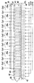
図16は、第1の実施例によるCCDイメージセンサ10aにおける垂直電荷転送素子20の各々を低スミア駆動させたときの各垂直電荷転送段の電位レベルの変化と、各垂直電荷転送段に分布する電荷の種類とを示す。垂直電荷転送素子20の各々は、8相の垂直駆動信号φV1〜φV8によって1/4間引き走査の下に駆動される。読出パルスPrは、垂直駆動信号φV1に重畳される。
【0251】
同図には、読出パルスPrが所定の垂直転送電極25に印加された時刻T1から所定の時刻T5までの間での、各垂直電荷転送段の電位レベルの変化と、各垂直電荷転送段に分布する電荷の種類とが示されている。1つの光電変換素子15から読み出された電荷をQとし、読出パルスPrの印加前の段階で各垂直電荷転送段に分布していた雑音電荷の各々をSとする。
【0252】
低スミア駆動では、まず、垂直駆動信号φV1およびφV3〜φV7をハイレベルとし、これと同時に垂直駆動信号φV2およびφV8をローレベルとする。垂直駆動信号φV1、φV3〜φV7が供給される各垂直電荷転送段の電位レベルが、ポテンシャル・ウェルとして機能するレベルWになる。また、垂直駆動信号φV2、φV8が供給される各垂直電荷転送段の電位レベルが、ポテンシャル・バリアとして機能するレベルBになる。
【0253】
垂直電荷転送段がレベルBになると、この垂直電荷転送段に分布していた雑音電荷Sは、上流側または下流側のポテンシャル・ウェルに移動する。ポテンシャル・バリアとポテンシャル・ウェルとが同時に形成された場合、ポテンシャル・バリアとなった垂直電荷転送段に分布していた雑音電荷Sが上流側および下流側のどちらのポテンシャル・ウェルに移動するかは、特定できない。ここでは、便宜上、上流側のポテンシャル・ウェルに移動するものとする。
【0254】
次に、時刻T1において、垂直駆動信号φV1に読出パルスPrを重畳する。読出パルスPrが供給された垂直電荷転送段に、所定の光電変換素子15から電荷Qが読み出され、これらの垂直電荷転送段の各々において、電荷Qと2つの雑音電荷Sとが混合される。2つの雑音電荷Sのうちの一方は、この垂直電荷転送段に予め分布していた雑音電荷Sであり、他の一方は、下流側のポテンシャル・バリアから移動してきた雑音電荷Sである。混合されたこれらの電荷を記号「Q+2S」で表す。
【0255】
このとき、垂直駆動信号φV3〜φV7が供給されている各垂直電荷転送段は互いに連なって、5つの垂直電荷転送段に亘るポテンシャル・ウェルを形成する。このポテンシャル・ウェルにおいて、計6つの雑音電荷Sが混合される。混合されたこれらの雑音電荷を記号「6S」で表す。また、M個(Mは1以上の整数を表す。以下同じ。)の垂直電荷転送段に亘るポテンシャル・ウェルを「M連のポテンシャル・ウェル」といい、M個の垂直電荷転送段に亘るポテンシャル・バリアを「M連のポテンシャル・バリア」という。
【0256】
次いで、時刻T2において垂直駆動信号φV3およびφV4がハイレベルからローレベルに転じる。垂直駆動信号φV3〜φV4が供給されている各垂直電荷転送段のレベルがレベルBになる。
【0257】
その結果、上記5連のポテンシャル・ウェルの上流端が下流側に2垂直電荷転送段分移動して、3連のポテンシャル・ウェルとなる。その一方で、ポテンシャル・ウェルの下流側にあった1連のポテンシャル・バリアが下流側に2垂直電荷転送段分伸長して、3連のポテンシャル・バリアとなる。
【0258】
次に、時刻T3において垂直駆動信号φV2およびφV3がローレベルからハイレベルに転じる。垂直駆動信号φV2〜φV3が供給されている各垂直電荷転送段のレベルがレベルWになる。
【0259】
その結果、上記1連のポテンシャル・ウェルが下流側に2垂直電荷転送段分伸長して、3連のポテンシャル・ウェルとなる。その一方で、ポテンシャル・ウェルの下流側にあった上記3連のポテンシャル・バリアの上流端が下流側に2垂直電荷転送段分移動して、1連のポテンシャル・バリアとなる。
【0260】
この後、時刻T4におけるように、ポテンシャル・ウェルの上流端を下流側に1垂直電荷転送段分移動させて、2連のポテンシャル・ウェルとする。その一方で、ポテンシャル・ウェルの下流側にあった1連のポテンシャル・バリアを下流側に1垂直電荷転送段分伸長させて、2連のポテンシャル・バリアとする。
【0261】
次いで、時刻T5におけるように、上記2連のポテンシャル・ウェルを下流側に1垂直電荷転送段分伸長させて、3連のポテンシャル・ウェルとする。その一方で、ポテンシャル・ウェルの下流側にあった上記2連のポテンシャル・バリアの上流端を下流側に1垂直電荷転送段分移動させて、2連のポテンシャル・バリアとする。
【0262】
時刻T4での動作と時刻T5での動作とをこの順番で交互に繰り返すことにより、雑音電荷6sと電荷(Q+2S)とを順次下流へ転送することができる。
【0263】
図17に示すように、CCDラインメモリ部35へは、雑音電荷6Sが同じタイミングで転送されてくる。したがって、これらの雑音電荷6Sの全てを一斉に、水平電荷転送素子40を介して掃出ドレイン45へ容易に排出することができる。
【0264】
電荷(Q+2S)にのみ基づいて、画像データを生成することができる。スミアの要因となる雑音電荷の量が低減されるので、より良好な画像を表示ないし記録することができる。
【0265】
以上、実施例によるCCD撮像システムならびにCCDイメージセンサおよびその駆動方法について説明したが、本発明は上述した実施例に限定されるものではない。
【0266】
例えば、実施例によるCCDイメージセンサの各々では、各水平転送電極を電圧供給線に接続する前の段階での数で、1つの水平電荷転送段当たり第1〜第2水平転送電極を1個ずつ配置した。しかしながら、水平電荷転送チャネルの構造は変えずに、各水平転送電極を電圧供給線に接続する前の段階での水平転送電極の数を、1つの水平電荷転送段当たり1個にすることもできる。この場合、第1および第2水平転送電極がそれぞれ覆っていた領域が、1個の水平転送電極で覆われる。補助水平電荷転送段についても同様である。
【0267】
また、水平電荷転送素子は、1本のn型チャネルにn+ 型不純物添加領域とn型不純物添加領域とを所定のパターンで繰り返し形成し、このn型チャネル上に膜厚がほぼ一定の電気的絶縁膜を介して所定数の転送電極を形成したタイプの電荷転送素子によって構成することもできる。
【0268】
このとき、各水平転送電極を電圧供給線に接続する前の段階での数で、個々のn+ 型不純物添加領域の上方に電気的絶縁膜を介して1個ずつ水平転送電極が配置され、個々のn型不純物添加領域の上方にも電気的絶縁膜を介して1個ずつ水平転送電極が配置される。あるいは、1つのn+ 型不純物添加領域とその直ぐ上流側の1つのn型不純物添加領域とによって構成される1組の不純物添加領域に1個ずつ、この組を構成する不純物添加領域の両方を平面視上覆う水平転送電極が電気絶縁膜を介して配置される。また、上記のn+ 型不純物添加領域に代えてn型不純物添加領域を形成し、上記のn型不純物添加領域に代えてn型不純物添加領域とその上に形成されたp- 型不純物添加領域とによって構成される領域を形成してもよい。
【0269】
n型不純物の濃度がほぼ一定である1本のn型チャネルの上に、膜厚が相対的に厚い領域(以下、この領域を「厚肉領域」という。)と相対的に薄い領域(以下、この領域を「薄肉領域」という。)とを所定のパターンで繰り返し配置した電気的絶縁膜を形成し、この電気的絶縁膜上に所定数の転送電極を形成したタイプの電荷転送素子によって水平電荷転送素子を構成することもできる。
【0270】
このとき、各水平転送電極を電圧供給線に接続する前の段階での数で、厚肉領域および薄肉領域それぞれの上に1個ずつ、水平転送電極が形成される。あるいは、1つの厚肉領域とその直ぐ上流側の1つの薄肉領域とによって構成される1組の領域に1個ずつ、この組を構成する厚肉領域および薄肉領域の両方を平面視上覆う水平転送電極が電気絶縁膜を介して配置される。
【0271】
さらには、n型不純物の濃度がほぼ一定である1本のn型チャネルの上に、膜厚がほぼ一定の電気的絶縁膜を形成し、この電気的絶縁膜上に所定数の転送電極を形成したタイプの電荷転送素子によって水平電荷転送素子を構成することもできる。
【0272】
このとき、個々の水平転送電極に相対的に高いレベルの電圧を印加することにより、この水平転送電極の下に位置するn型チャネルの一領域にポテンシャル・ウェル領域を形成することができる。個々の水平転送電極に相対的に低いレベルの電圧を印加することにより、この水平転送電極の下に位置するn型チャネルの一領域にポテンシャル・バリア領域を形成することができる。
【0273】
いずれのタイプの電荷転送素子を水平電荷転送素子として利用する場合でも、1つの垂直電荷転送素子に対応して1つの水平電荷転送段が形成される。個々の水平電荷転送段は、唯1つのポテンシャル・バリア領域と、唯1つのポテンシャル・ウェル領域とを有する。垂直電荷転送素子に対応する各水平電荷転送段は、互いに隣接しつつ一列に配置される。
【0274】
水平電荷転送素子における水平転送電極の各々は、これらの水平転送電極を電圧供給線に接続した後の段階での数を基準にしてみたときに、複数の群に分けることができる。1つの群は、光電変換素子行方向に連続するm個(mは3以上の整数を表す。)の水平転送電極によって構成され、1つの群を構成するm個の水平転送電極の各々は、互いに異なる電圧供給線に接続されている。m個を周期とする水平転送電極の各々は、同一の電圧供給線に接続されている。mの値は、例えば3、4、6、7、8等、水平電荷転送素子の駆動方法等に応じて適宜選定可能である。
【0275】
水平電荷転送素子に補助水平電荷転送段を設けるか否かは、適宜選択可能である。
【0276】
垂直電荷転送素子は、補助転送電極を含めずに構成することもできる。垂直電荷転送素子の駆動方法は、1/2間引き走査やインターレース走査に基づく駆動方法に限定されるものではない。素子の構造、撮像モード、垂直加算の態様等に応じて、1/8間引き走査、1/16間引き走査、プログレッシブ走査等、適宜選定可能である。
【0277】
CCDラインメモリ部における転送制御段の構成も、水平電荷転送素子と同様に、適宜選定可能である。転送制御段は、水平電荷転送素子における水平電荷転送段と同様にして構成することができる。
【0278】
図18に示すように、掃出ドレインは、パンチスルータイプにすることもできる。同図に示した構成要素のうち、パンチスルータイプの掃出ドレイン145以外の構成要素は、既に図6(A)において示されているので、図6(A)に示した構成要素と共通するものについては、図6(A)で用いた参照符号と同じ参照符号を付してその説明を省略する。
【0279】
図18に示したパンチスルータイプの掃出ドレイン145は、水平電荷転送チャネル41から所定の間隔を開けてp型不純物添加領域11bに形成されたドレイン領域140を有している。このドレイン領域140は、n+ 型不純物添加領域によって構成され、光電変換素子行方向に延在する。
【0280】
n型不純物添加領域141が、ドレイン領域140における水平電荷転送チャネル41側に隣接配置され、このn型不純物添加領域141における水平電荷転送チャネル41側に、ポテンシャル・バリア領域142が隣接配置されている。バリア領域142は、例えば、p型不純物添加領域11bの所定箇所に形成されたn- 型もしくはp- 型の不純物添加領域によって構成される。n型不純物添加領域141とポテンシャル・バリア領域142とは、共に、光電変換素子行方向に延在する。ポテンシャル・バリア領域142は、水平電荷転送チャネル41とも隣接する。
【0281】
なお、n- 型不純物添加領域におけるn型不純物の濃度は、n型不純物添加領域におけるn型不純物の濃度よりも低い。p- 型不純物添加領域におけるp型不純物の濃度は、p型不純物添加領域におけるp型不純物の濃度よりも低い。
【0282】
ドレイン領域140の上方に、電気的絶縁膜23を介してドレイン電極143が配置されている。ドレイン電極143は、例えば第1ポリシリコン層によって形成される。電気的絶縁膜(熱酸化膜)50が、ドレイン電極143を覆っている。
【0283】
n型不純物添加領域141上に、電気的絶縁膜23を介して、更に電気的絶縁膜144が形成されている。電気的絶縁膜144は、例えば、CVD(化学的気相堆積法)によって電気的絶縁膜23上に堆積されたシリコン酸化物によって構成される。
【0284】
水平電荷転送素子40における第1〜第2水平転送電極42、43の各々は、水平電荷転送チャネル41の所定領域を覆う他、p- 型不純物添加領域142をも覆う。更に、電気的絶縁膜144をも覆う。n型不純物添加領域141はポテンシャル・ウェル領域として機能する。
【0285】
ドレイン電極143に供給される制御信号がローレベルのときには、水平電荷転送素子40における水平電荷転送段の各々に供給される水平駆動信号がローレベルおよびハイレベルのいずれであっても、ポテンシャル・バリア領域142の電位の方が水平電荷転送段の電位より低くなる。水平電荷転送段内の電荷は、掃出ドレイン145へ排出されることなく、水平電荷転送段内に留まる。
【0286】
水平電荷転送段の各々にローレベルの水平駆動信号を印加し、ドレイン電極143にハイレベルの制御信号を印加すると、ドレイン領域140の電位が高まる。この影響により、n型不純物添加領域141の電位がドレイン領域140の電位とほぼ同等になり、これに伴ってポテンシャル・バリア領域142の電位も高まる。ポテンシャル・バリア領域142の電位が、ローレベルの水平駆動信号が供給されている水平電荷転送段の電位より高くなる。
【0287】
その結果として、ローレベルの水平駆動信号が供給されている水平電荷転送段に分布していた電荷が、ポテンシャル・バリア領域142およびn型不純物添加領域141を介して、ドレイン領域140へ排出される。ドレイン領域140へ排出された電荷は、掃出ドレイン145の制御信号の電源に吸収される。
【0288】
その他、CCDラインメモリ部の構成も、水平電荷転送素子と同様に、適宜変更可能である。1つのポテンシャル・バリア領域と1つのポテンシャル・ウェル領域とを有する転送制御段を形成することができる構成であれば基本的によい。
【0289】
垂直電荷転送素子は、補助転送電極を含めずに構成することもできる。垂直電荷転送素子の駆動方法は、インターレース走査や1/2間引き走査に基づく駆動方法に限定されるものではない。プログレッシブ走査、1/4間引き走査、1/8間引き走査、1/16間引き走査等、撮像モード等に応じて適宜選定可能である。
【0290】
水平電荷転送素子の駆動方法も、光電変換素子行方向の電荷を1/2または1/3に間引きく駆動方法に限定されるものではない。例えば、光電変換素子行方向の電荷を1/4以上に間引いて駆動させることも可能である。必要に応じて、水平電荷転送素子内で2または3以上の電荷同士を加算(混合)することも可能である。水平電荷転送素子の駆動方法に応じて、水平駆動信号の相数を、3、4、6、8相等、適宜選定することができる。
【0291】
CCDラインメモリ部から水平電荷転送素子へ電荷を転送する際の垂直電荷転送チャネルのグループ分け、すなわち、どの垂直電荷転送チャネルによって転送されてくる電荷を必要電荷とし、どの垂直電荷転送チャネルによって転送されてくる電荷を不要電荷とするかは、CCD撮像システムの撮像モード等に応じて、適宜選定可能である。
【0292】
例えばカラー撮像を行う場合には、必要電荷を転送する1つの垂直電荷転送チャネルグループを構成するサブグループの各々は、フルカラー情報を得るうえで必要となる種類数の電荷、例えば電荷g、電荷rおよび電荷bの3種類を転送する3〜4本程度の垂直電荷転送チャネルによって構成される。白黒撮像の場合には、1本の垂直電荷転送チャネルによって1つのサブグループを構成することも可能である。
【0293】
カラー撮像用のCCDイメージセンサでは、光遮蔽膜を設けることが好ましい。カラー撮像用の単板式CCDイメージセンサでは、色フィルタアレイが設けられる。マイクロレンズアレイは省略することも可能であるが、設けた方が好ましい。
【0294】
白黒撮像用のCCDイメージセンサでは、光遮蔽膜およびマイクロレンズアレイを省略することができる。色フィルタアレイを設けることは必須の要件ではないが、必要に応じて単色の色フィルタアレイを設けてもよい。
【0295】
カラー撮像用の単板式CCDイメージセンサに設けられる色フィルタアレイは、図3に示した配列パターンを有するものに限定されるものではない。また、原色型の色フィルタアレイに限定されるものではなく、補色型の色フィルタアレイであってもよい。
【0296】
原色型の色フィルタアレイにおける色フィルタの配列パターンとしては、ベイヤー型、インターライン型、GストライプRB市松型、GストライプRB完全市松型、ストライプ型、斜めストライプ型等と呼ばれる配列パターンが知られている。これらの配列パターンを平面上で40°程度回転させれば、多数個の光電変換素子が画素ずらし配置されたCCDイメージセンサに適用することが可能な原色型の色フィルタアレイを得ることができる。
【0297】
補色型の色フィルタアレイにおける色フィルタの配列パターンとしては、フィールド色差順次型、フレーム色差順次型、MOS型、改良MOS型、フレームインタリーブ型、フィールドインタリーブ型、ストライプ型等と呼ばれる配列パターンが知られている。これらの配列パターンを平面上で40°程度回転させれば、多数個の光電変換素子が画素ずらし配置されたCCDイメージセンサに適用することが可能な補色型の色フィルタアレイを得ることができる。
【0298】
CCDイメージセンサは、インターライン転送型に限らず、フルフレーム型、フレーム転送型、フレームインターライン転送型、全画素読出型等であってもよい。
【0299】
その他、種々の変更、改良、組み合わせ等が可能であることは当業者に自明であろう。
【0300】
【発明の効果】
以上説明したように、本発明によれば、所望の電荷を間引くことを可能にする電荷転送装置が提供される。この電荷転送装置をCCDイメージセンサの水平電荷転送素子として用いることにより、複数の垂直電荷転送素子それぞれに読み出された電荷の中から所望の電荷だけを水平電荷転送素子によって転送することが可能になる。
【0301】
CCDイメージセンサを備えたCCD撮像システムにおいて、垂直画素数と水平画素数の両方が間引かれた画像データを容易に得ることが可能になる。良好なモニター表示を行うCCD撮像システムを提供することが容易になる。
【図面の簡単な説明】
【図1】実施例によるCCD撮像システムの概略を示すブロック図である。
【図2】第1の実施例によるCCDイメージセンサにおける光電変換素子とその周辺を概略的に示す断面図である。
【図3】第1の実施例によるCCDイメージセンサが備えている色フィルタアレイの一部を示す平面図である。
【図4】第1の実施例によるCCDイメージセンサを概略的に示す部分平面図である。
【図5】第1の実施例によるCCDイメージセンサのCCDラインメモリ部から掃出ドレインにかけての領域を拡大して示す概略図である。
【図6】図6(A)は、図5に示したB−B線に沿った断面の概略図であり、図6(B)は、図5に示したC−C線に沿った断面の概略図である。
【図7】水平電荷転送素子から掃出ドレインへ選択的に不要電荷を排出する際になされる垂直電荷転送チャネルのグループ分けの1つの仕様を示す部分平面図である。
【図8】第1の実施例によるCCDイメージセンサのCCDラインメモリ部、水平電荷転送素子および掃出ドレインをそれぞれ駆動させる際の制御信号φLM、水平駆動信号φH1〜φH8および制御信号φDRの波形の一例を示すタイミングチャートである。
【図9】第1の実施例によるCCDイメージセンサにおいてCCDラインメモリ部から水平電荷転送素子へ、また、CCDラインメモリ部から水平電荷転送素子を介して掃出ドレインへ電荷を転送する際の原理を模式的に示す
【図10】図10(A)〜図10(B)は、図8に示した時刻t1〜t2での電荷の分布の様子を示す模式図である。
【図11】第1の実施例によるCCDイメージセンサにおける水平電荷転送素子を4相の水平駆動信号によって駆動させる際の配線例を概略的に示す部分平面図である。
【図12】第1の実施例によるCCDイメージセンサのCCDラインメモリ部、水平電荷転送素子および掃出ドレインそれぞれを駆動させる際の制御信号φLM、水平駆動信号φH1〜φH8および制御信号φDRの波形の他の一例を示すタイミングチャートである。
【図13】図13(A)〜図13(C)は、図12に示した時刻T1〜T2での電荷の分布の様子を示す模式図である。
【図14】図12に示した時刻T3での電荷の分布の様子を示す模式図である。
【図15】第2の実施例によるCCDイメージセンサにおける光電変換素子、垂直電荷転送素子、CCDラインメモリ部、水平電荷転送素子、掃出ドレインおよび出力部の平面配置を概略的に示す部分平面図である。
【図16】第1の実施例によるCCDイメージセンサにおける垂直電荷転送素子の各々を低スミア駆動させたときの各垂直電荷転送段の電位レベルの変化と、各垂直電荷転送段に分布する電荷の種類とを示す模式図である。
【図17】雑音電荷が掃出ドレインへ排出される際の電荷の分布の様子を示す模式図である。
【図18】パンチスルータイプの掃出ドレインを模式的に示す部分断面図である。
【符号の説明】
10、10a、10b…CCDイメージセンサ、 11…半導体基板、 15…光電変換素子、 16…光電変換素子領域、 20…垂直電荷転送素子、 20a…垂直電荷転送チャネル、 21…読出ゲート、 21a…読出ゲート用チャネル領域、 25、25a…第1垂直転送電極、 26、26a…第2垂直転送電極、 35…CCDラインメモリ部、 35a…転送制御段、 36…第1転送制御電極、 37…第2転送制御電極、 40…水平電荷転送素子、 40a…水平電荷転送段、 40b…補助水平電荷転送段、 41…水平電荷転送チャネル、 42…第1水平転送電極、 43…第2水平転送電極、 45、145…掃出ドレイン、 46、140…ドレイン領域、 47a…掃出ゲート電極、 47b…掃出ゲート用チャネル領域、 55…色フィルタアレイ、 60…出力部、 65…駆動回路、 70…映像信号処理回路、 80…表示部、 100…CCD撮像システム。[0001]
[Industrial application fields]
The present invention includes a charge transfer device capable of receiving a plurality of charges in parallel and outputting these charges in series, a driving method thereof, a CCD image sensor having the charge transfer device, and the CCD image sensor. The present invention relates to a CCD imaging system.
[0002]
[Prior art]
For example, a charge transfer element can be obtained by forming a strip-shaped n-type channel in a semiconductor substrate and arranging a plurality of electrodes adjacent to each other in parallel via an electrical insulating film on the n-type channel. At this time, the individual electrodes are arranged so as to cross the n-type channel in plan view. Charge transfer devices having an n-type channel can be roughly classified into the following three types.
[0003]
The first type of charge transfer element is a charge transfer element in which the concentration of the n-type impurity in the n-type channel is substantially constant, and the thickness of the electrical insulating film on the n-type channel is also substantially constant.
[0004]
In this type of charge transfer device, the potential well region is relatively low under the electrode to which a relatively high level of voltage is applied, depending on the relative magnitude of the voltage applied to each electrode. A potential barrier region is formed under the electrode to which a level voltage is applied. If a potential barrier region is formed on the upstream side and downstream side of the potential well region, charges can be confined in the potential well region.
[0005]
By appropriately controlling the height of the voltage applied to each electrode, the potential well region sandwiched between the two potential barrier regions can be sequentially moved in a desired direction. The charge can be transferred in a desired direction.
[0006]
In this specification, the movement of the charges transferred by the charge transfer element is regarded as one flow, and the relative positions of the individual members and the like are set to “what upstream”, “ It shall be specified as “downstream” or the like.
[0007]
The second type of charge transfer element is a region in which the concentration of n-type impurities is relatively high (hereinafter, this region is referred to as “n”+This is referred to as a “type impurity doped region”. ) And a relatively low region (hereinafter, this region is referred to as an “n-type impurity doped region”) is a charge transfer element formed alternately in an n-type channel.
[0008]
In this type of charge transfer device, typically n+One electrode is disposed on each of the impurity doped region and the n doped region via an electrical insulating film. An electrode disposed on one n-type impurity doped region and n on the downstream side thereof+The electrode arranged on the type impurity added region is connected in common. One n-type impurity doped region and n downstream thereof+One electrode covering the type impurity doped region may be formed on these regions.
[0009]
Individual n+The type impurity doped region is always a potential well region with respect to the n type impurity doped region. The charge in the potential well region is prohibited from moving by the potential barrier region. Charges can be transferred in the direction from the potential barrier region to the potential well region.
[0010]
This will be described more specifically. A certain n+Type impurity doped region+N-type impurity added region A ”, an n-type impurity added region immediately downstream thereof is referred to as“ n-type impurity added region B ”, and an n-type impurity added region B immediately downstream of this“ n-type impurity added region B ”+Type impurity doped region+Type impurity doped region C ". On the regions B and C, electrodes connected in common are arranged.
[0011]
n+When charge is distributed in the type impurity doped region A (potential well region), the n type impurity doped region B, n+When a relatively high voltage is applied to the electrode on the type impurity doped region C, the n type impurity doped region B becomes n+It does not function as a potential barrier region for the type impurity doped region A. n+The type impurity doped region C is always a potential well region with respect to the n type impurity doped region B. Therefore, n+The charge distributed in the type impurity doped region A is n through the n type impurity doped region B.+It moves to the type impurity addition region C.
[0012]
The n-type impurity doped region B is n+It functions as a potential barrier region for the type impurity doped region C. n-type impurity doped region B, n+Even if the voltage applied to the electrode on the type impurity doped region C is restored to the original level, n+The charge transferred to the type impurity doped region C is n+There is no return to the type impurity added region A.
[0013]
In the third type of charge transfer device, the n-type impurity concentration in the n-type channel is substantially constant, and the electrically insulating film on the n-type channel is a relatively thick region (hereinafter referred to as “ This is a charge transfer device in which relatively thick regions (hereinafter sometimes referred to as “thin regions”) and alternately thin regions (hereinafter sometimes referred to as “thin regions”).
[0014]
Usually, one electrode is disposed on each of the thick and thin regions. The electrode arranged on one thin area and the electrode arranged on the thick area on the downstream side thereof are connected in common. One electrode that covers one thin region and a thick region downstream thereof may be formed on these regions.
[0015]
In this type of charge transfer device, even if a constant voltage is applied to each electrode, when the n-type channel is a buried channel, the potential barrier region is formed below the thin region and the potential well region is formed below the thick region. Is formed. Charges can be transferred in the direction from the potential barrier to the potential well.
[0016]
As a representative electronic device using a charge transfer element, there is a CCD (Charge Coupled Element) image sensor. It can be roughly divided into a CCD linear (line) image sensor and a CCD area image sensor.
[0017]
A CCD area image sensor usually includes two types of charge transfer elements. One is a charge transfer element called VCCD or vertical charge transfer element, and the other is a charge transfer element called HCCD or horizontal charge transfer element.
[0018]
In an interline CCD area image sensor, a large number of photoelectric conversion elements are arranged in a matrix over a plurality of rows and columns, and one VCCD is arranged for each photoelectric conversion element column. In many CCD area image sensors, each VCCD is electrically connected to one HCCD. A CCD area image sensor having a plurality of HCCDs is also known.
[0019]
The VCCD is generally constituted by a charge transfer element of a type in which the concentration of the n-type impurity in the n-type channel is substantially constant and the thickness of the electrical insulating film on the n-type channel is also substantially constant. This charge transfer element (VCCD) is usually driven by vertical drive signals of three or more phases. In each VCCD, one vertical charge transfer stage is constituted by one electrode and a region of the n-type channel located under this electrode. About 2 to 4 vertical charge transfer stages are arranged for one photoelectric conversion element.
[0020]
In HCCD, for example, n type channel has n+Type impurity doped regions and n type impurity doped regions are alternately formed, and a commonly connected electrode is disposed on a pair of adjacent impurity doped regions. One horizontal charge transfer stage is constituted by a pair of adjacent impurity-added regions and a commonly connected electrode thereon. Two horizontal charge transfer stages are arranged for one VCCD. This charge transfer element (HCCD) is normally driven by a two-phase horizontal drive signal.
[0021]
A CCD imaging system such as an electronic still camera has been developed using a CCD area image sensor.
[0022]
The electronic still camera includes a small monitor and is configured so that a user can select a still image recording mode for recording a still image and a monitor mode for displaying an image on a small monitor. The monitor mode is used, for example, when the user determines the angle of view of a still image.
[0023]
In recent years, the number of pixels of still images picked up by an electronic still camera has reached several million, and more than six million. On the other hand, the number of pixels when displaying a moving image in the monitor mode of an electronic still camera is generally about 100,000 to 400,000.
[0024]
For this reason, in the monitor mode, the photoelectric conversion elements from which charges are read out to the VCCD are limited to some photoelectric conversion element rows. Thinning scanning is performed to read out charges by thinning photoelectric conversion element rows to 1/2 or more. Alternatively, charges are mixed (vertical addition) within each VCCD. That is, the charges accumulated in each of the two or more photoelectric conversion elements adjacent in the photoelectric conversion element array direction in each photoelectric conversion element array are mixed (vertically added) in the VCCD corresponding to the photoelectric conversion element array. . If charges are added, the amount of signal (charge) handled as one pixel in signal processing increases, so that an advantage that the imaging sensitivity increases in accordance with the amount of addition can be obtained. Relatively bright images can be reproduced.
[0025]
In a CCD imaging system for color imaging, a color filter array is used to obtain full color information. The color filter array is composed of color filters of a plurality of colors arranged under a fixed repeating pattern, and one color filter corresponds to one photoelectric conversion element.
[0026]
[Problems to be solved by the invention]
Image data in which the number of vertical pixels is thinned out can be obtained by performing either or both of thinning scanning and mixing (vertical addition) of charges in the VCCD.
[0027]
However, no HCCD has yet been proposed that can thin out the charge received simultaneously (in parallel) from each of the electrically connected VCCDs. Similarly, an HCCD capable of mixing charges (horizontal addition) has not been proposed yet.
[0028]
An object of the present invention is to provide a charge transfer device that makes it possible to thin out a desired charge.
[0029]
Another object of the present invention is to provide a method of driving a charge transfer device that makes it possible to thin out a desired charge.
[0030]
Still another object of the present invention is to provide a CCD image sensor that enables only a desired charge to be transferred by the HCCD from among the charges read to the VCCD.
[0031]
Still another object of the present invention is to provide a CCD imaging system capable of transferring only a desired charge from the charges read out to the VCCD by the HCCD.
[0032]
[Means for Solving the Problems]
According to one aspect of the present invention,
A semiconductor substrate;
One surface of the semiconductor substrate~ sideA plurality of first charge transfer channel regions of the first conductivity type formed in the final stage and having a line memory section in the final stageAnd a plurality of first charge transfer electrodes;A second charge transfer channel region of a first conductivity type electrically connectable to each of the first charge transfer channel regions;And a plurality of second charge transfer electrodesA charge transfer device comprising:The same voltage is periodically applied to the second charge transfer electrodes in units of m, and when the charges are transferred from the line memory unit to the second charge transfer channel region, the m second electrodes are one cycle. Voltage is applied to the charge transfer electrode at different timings divided into multiple timesA charge transfer element;
Said second charge transfer channelregionAlong the one surface of the semiconductor substrate~ sideFormed in the second charge transfer channelregionDrain region of first conductivity type electrically connectable toAnd in synchronization with the application timing of the voltage to the second charge transfer electrode,Second charge transferChannel region and drain regionSwitch means for switching the electrical connection between andA swept drain containing
Charge transfer device comprising
Is provided.
[0033]
According to another aspect of the invention,
A method of driving the above charge transfer device,
The potential of the line memory unit and theSecond charge transfer electrodeDrive powerPressureBy setting a part of the first charge transfer channel regionSecond charge transfer channel regionFurther, the charge is transferred by the setting of the switch means.SecondCharge transferChannel regionFrom the aboveDrain regionA first charge discharging step of discharging to
In the first charge discharging step,SecondCharge transferChannel regionA first charge transfer step of transferring charge from the first charge transfer channel region that does not transfer charge to the charge transfer element;
In the first charge transfer step,SecondCharge transferChannel regionThe charge transferred toSecondCharge transferChannel regionA second charge transfer step of transferring in a certain direction
Method for driving charge transfer device including
Is provided.
[0038]
By configuring the CCD image sensor as described above, a plurality of first charge transfer channel regions electrically connected to the horizontal charge transfer element are divided into a plurality of groups, and the first charge transfer channel region and thus the vertical charge Charges can be selectively transferred from the transfer element to the horizontal charge transfer element in units of groups. Further, the charges in the horizontal charge transfer element can be discharged to the sweep drain.
[0039]
As a result of these, only a desired charge can be transferred by the horizontal charge transfer element from the charges read to the vertical charge transfer element.
[0040]
For example, only the first charge transfer channel region (transfer control stage) in which charges that do not need to contribute to the generation of image data (in this specification, such charges are referred to as “unnecessary charges”) is distributed. Thus, unnecessary charges can be transferred from the first charge transfer channel region (transfer control stage) to the horizontal charge transfer element, and the unnecessary charges can be discharged to the sweep drain.
[0041]
After this, only the first charge transfer channel region (transfer control stage) in which charges that contribute to the generation of image data (in this specification, such charges are referred to as “necessary charges”) is distributed. The necessary charge is transferred from the first charge transfer channel region (transfer control stage) to the horizontal charge transfer element. By transferring this necessary charge to, for example, an output amplifier by a horizontal charge transfer element, a desired image signal can be obtained. By supplying this image signal to, for example, a video signal processing circuit, desired image data can be obtained.
[0042]
An image in which both the number of vertical pixels and the number of horizontal pixels are thinned by combining at least one of thinning scanning and mixing (vertical addition) of charges in the vertical charge transfer element and the above-described unnecessary charge discharging operation. Data can be easily generated. It becomes easy to obtain a good reproduction image (monitor image).
[0043]
In addition, it becomes possible to discharge charges that cause smear from the horizontal charge transfer element to the sweep drain during the thinning scanning.
[0044]
DETAILED DESCRIPTION OF THE INVENTION
FIG. 1 is a block diagram illustrating an outline of a CCD imaging system according to an embodiment. As shown in the figure, the
[0045]
The imaging
[0046]
The
[0047]
The
[0048]
The video
[0049]
The image
[0050]
The
[0051]
The
[0052]
The
[0053]
The
[0054]
The pulse
[0055]
The
[0056]
FIG. 2 is a sectional view schematically showing a photoelectric conversion element and its periphery in the
[0057]
In the
[0058]
In the
[0059]
On the right side of each
[0060]
A p-type
[0061]
The
[0062]
Further, further downstream than the most downstream photoelectric conversion element row,
[0063]
Each impurity added region can be formed by, for example, ion implantation and subsequent annealing. The p-type impurity doped
[0064]
The electrically insulating
[0065]
The electrical insulating
[0066]
First to second
[0067]
Each of the
[0068]
One region of the first
[0069]
When a read pulse to be described later is applied to the first
[0070]
The
[0071]
The
[0072]
A
[0073]
The
[0074]
The
[0075]
A
[0076]
In each of the primary color filter array and the complementary color filter array, one color filter is disposed above each
[0077]
The
[0078]
A
[0079]
A
[0080]
These
[0081]
FIG. 3 is a plan view showing a part of the
[0082]
In the
[0083]
The green color filter G1 constituting the first color filter row FC1 and the green color filter G2 constituting the third color filter row FC3 are merely changed in reference numerals for convenience, and both are formed of the same material. .
[0084]
In addition, the area | region enclosed with the broken line shown in each color filter in FIG. 3 shows the outline of the photoelectric conversion element area |
[0085]
FIG. 4 is a partial plan view schematically showing the
[0086]
As shown in FIG. 4, in the
[0087]
One vertical
[0088]
The first to second
[0089]
Each first
[0090]
The first to second
[0091]
The first to third
[0092]
The first to second
[0093]
The second
[0094]
In each of the vertical
[0095]
Each of the vertical charge transfer stages configured to include one vertical
[0096]
On the other hand, the region facing each of the first
[0097]
These
[0098]
The downstream end of each vertical
[0099]
A
[0100]
The
[0101]
An
[0102]
Hereinafter, the configurations of the CCD
[0103]
FIG. 5 is a schematic diagram showing an enlarged region from the CCD
[0104]
6A is a schematic view of a cross section taken along line VIA-VIA shown in FIG. 5, and FIG. 6B is a schematic view of a cross section taken along line VIB-VIB shown in FIG. is there.
[0105]
As shown in FIG. 5 or FIG. 6A, the downstream end of each vertical
[0106]
As shown in FIG. 6A, each of the vertical
[0107]
The width of the potential barrier region 20aB (width in the photoelectric conversion element column direction) is, for example, about 0.5 to 1 μm, and the width of the potential well region 20aW (width in the photoelectric conversion element column direction) is, for example, 2 to 20 μm. Degree. In any of the regions 20aB and 20aW, the conductivity type as a charge transfer channel is n-type.
[0108]
The first
[0109]
Each
[0110]
The first
[0111]
The charge transfer from the
[0112]
As shown in FIG. 5, the horizontal
[0113]
As shown in FIGS. 6A and 6B, the horizontal
[0114]
The
[0115]
The first barrier region 41B1 separates the
[0116]
Each of the first
[0117]
Each second
[0118]
These first and second
[0119]
One first
[0120]
The first and second
[0121]
When transferring charges from the
[0122]
When charges are transferred in the horizontal
[0123]
As shown in FIG. 5, FIG. 6A or FIG. 6B, the
[0124]
A sweep
[0125]
The
[0126]
The
[0127]
The individual
[0128]
The
[0129]
FIG. 4 additionally shows an example of wiring when each of the vertical
[0130]
As shown in FIG. 4, in order to drive each of the vertical
[0131]
As shown in FIG. 5, in order to drive the horizontal
[0132]
The horizontal drive signal φH1 is supplied to one group, the horizontal drive signal φH2 is supplied to the other group, and the horizontal drive signal φH3 is supplied to the remaining groups. In the illustrated example, the horizontal drive signal φH1 is supplied to the most downstream auxiliary horizontal charge transfer stage, and the horizontal drive signal φH2 is supplied to the second auxiliary horizontal charge transfer stage from the downstream. A horizontal drive signal φH3 is supplied to the most upstream auxiliary horizontal charge transfer stage (third auxiliary horizontal charge transfer stage from the downstream).
[0133]
As shown in FIGS. 4 and 5, the control signal φLM is supplied to each of the first to second
[0134]
In the present specification, the number of horizontal transfer electrodes in the horizontal charge transfer element after being connected to a voltage supply line that supplies a drive signal is counted under the following promise.
[0135]
That is, a plurality of horizontal transfer electrodes that are adjacent to each other and connected to the same voltage supply wiring are collectively counted as one. Under this promise, the number of two horizontal transfer electrodes that are adjacent to each other but are connected to different voltage supply lines is two. Also, the number of two horizontal transfer electrodes that are connected to the same voltage supply wiring but are separated from each other is two.
[0136]
The above convention shall also apply in the following cases: That is, a plurality of first charge transfer channel regions (for example, downstream end portions in each of the plurality of vertical
[0137]
According to the above convention, the horizontal
[0138]
In the CCD imaging system 100 (see FIG. 1), drive signals φV1 to φV4, control signals φLM, and φH1 to φH3 having a predetermined waveform are driven depending on whether the imaging mode is the still image recording mode or the monitor mode. 65 to the
[0139]
Hereinafter, an example of operations of the vertical
[0140]
When the imaging mode of the
[0141]
When each vertical
[0142]
The charges read to each of the vertical
[0143]
As shown in FIG. 7, in the monitor mode, each vertical
[0144]
Since all the constituent elements shown in FIG. 7 are shown in FIG. 5, the same reference numerals as those used in FIG.
[0145]
Hereinafter, a method of transferring unnecessary charges to the horizontal
[0146]
In the following description, the charge transferred through each vertical
[0147]
FIG. 8 shows an example of the waveforms of the control signal φLM, the horizontal drive signals φH1 to φH3, and the control signal φDR when only the necessary charges are transferred from the CCD
[0148]
FIG. 9 schematically shows the principle of transferring charges from the CCD
[0149]
10A schematically shows the state of charge distribution at time t1 shown in FIG. 8, and FIG. 10B schematically shows the state of charge distribution at time t2 shown in FIG. Show.
[0150]
9, FIG. 10A, and FIG. 10B are all shown in FIG. 6A or FIG. 7, each component is shown in FIG. 6A or FIG. The same reference numerals as those used in FIG.
[0151]
As shown in FIG. 8, at time t0 before transferring charges from the CCD
[0152]
As shown in FIG. 9, when the horizontal drive signal φHn (n represents an arbitrary integer of 1 to 8, the same applies hereinafter) is at the low level L, the horizontal
[0153]
Therefore, at time t0 shown in FIG. 8, no charge is transferred from the CCD
[0154]
As shown at time t1 in FIG. 8, when transferring unnecessary charges from the CCD
[0155]
As shown in FIG. 9, when the horizontal drive signal φHn is at the high level H and the control signal φLM is at the low level L, the horizontal charge transfer channel 46 (potential barrier region) below the first
[0156]
At this time, when the control signal φDR is at a low level L (for example, 5 V), the sweep
[0157]
On the other hand, when the control signal φDR is at the high level H, the vicinity of the surface of the sweep
[0158]
Therefore, at time t1 shown in FIG. 8, charges are transferred from the CCD
[0159]
FIG. 10A shows the distribution state of the charges g1, r, g2, and b at time t1 shown in FIG. Unnecessary charges r and g2 are transferred from each of the vertical
[0160]
No charge is transferred from the CCD
[0161]
Next, the horizontal drive signals φH2 and φH3 are changed from the high level H to the low level L. Subsequently, the control signal φLM is changed from the low level L to the high level H, and the transfer of charges from the CCD
[0162]
Thereafter, the horizontal drive signals φH3, φH2, and φH1 are sequentially changed from the low level L to the high level H in this order while maintaining the control signal φDR at the high level H. While the horizontal drive signal φH2 is at the high level H, the horizontal drive signal φH3 is returned from the high level H to the low level L. While the horizontal drive signal φH1 is at the high level H, the horizontal drive signal φH2 is returned from the high level H to the low level L. The horizontal drive signal φH1 returns to the low level L after a certain time has elapsed. This operation corresponds to an operation of transferring charges in the horizontal
[0163]
Even if there is a horizontal charge transfer stage in which unnecessary charges cannot be sufficiently discharged to the
[0164]
After the horizontal drive signal φH1 is returned from the high level H to the low level L, the control signal φLM is changed from the high level H to the low level L. Further, the control signal φD is changed from the high level H to the low level L, and the discharge of charges from the horizontal
[0165]
After that, as at time t2 in FIG. 8, only the horizontal drive signal φH1 is set to the high level again. The control signal φLM is at the low level L, and the control signal φDR is also at the low level L. Therefore, charges are transferred from the
[0166]
FIG. 10B shows the distribution state of the charges g1, r, g2 and b at time t2 shown in FIG. Necessary charges g1, r, g2 or b are transferred from each of the vertical
[0167]
Thereafter, the horizontal drive signal φH1 is changed from the high level H to the low level L, and then the control signal φLM is changed from the low level L to the high level H, thereby prohibiting charge transfer from the CCD
[0168]
As a result, each of the
[0169]
As described above, by controlling the
[0170]
The
[0171]
The
[0172]
Accordingly, it is easy to generate image data in which both the number of vertical pixels and the number of horizontal pixels are thinned out by thinning out desired charges in both the photoelectric conversion element column direction and the photoelectric conversion element row direction. As compared with the case where monitor display is performed based on pixel data obtained by thinning out only the number of vertical pixels, it is easy to obtain a good monitor image. A moving image can be displayed on a monitor, and a still image can be displayed on a monitor. Of course, it is also possible to generate image data in which only the number of horizontal pixels is thinned out by thinning out desired charges only in the photoelectric conversion element row direction.
[0173]
Since the number of charges transferred from the horizontal
[0174]
That is, the length of one horizontal readout period under the same data rate is longer than that of a conventional horizontal charge transfer element that receives charges from all vertical charge transfer elements and transfers all of these charges to the output unit. It is shortened to about 1/3. Accordingly, the frame frequency at the time of monitor display can be increased almost three times, and it becomes easy to perform more natural monitor display. When monitor display is performed at the same frame frequency as in the prior art, the data rate is approximately 1/3, so that the driving frequency of the horizontal charge transfer element can be reduced to approximately 1/3. As a result, it is possible to reduce the driving power of the horizontal charge transfer element, which is a main power consumption source in the CCD imaging system, to approximately 1/3.
[0175]
On the other hand, when the imaging mode of the
[0176]
In the still image recording mode, each vertical
[0177]
First, charges are transferred from each vertical
[0178]
Charge transfer from the CCD
[0179]
At the time of charge transfer in the horizontal
[0180]
The
[0181]
Thereafter, image data is supplied from the image
[0182]
Of course, in the still image recording mode, a desired charge is thinned out in one or both of the photoelectric conversion element column direction and the photoelectric conversion element row direction, and either one or both of the number of vertical pixels and the number of horizontal pixels are in between. It is also possible to generate drawn image data.
[0183]
When the horizontal
[0184]
When the horizontal
[0185]
FIG. 11 shows wiring for supplying the horizontal
[0186]
The horizontal drive signal φH1 includes a horizontal charge transfer stage corresponding to the leftmost vertical
[0187]
The horizontal drive signal φH2 includes a horizontal charge transfer stage corresponding to the second vertical
[0188]
The horizontal drive signal φH3 includes a horizontal charge transfer stage corresponding to the fifth vertical
[0189]
The horizontal drive signal φH4 includes a horizontal charge transfer stage corresponding to the sixth vertical
[0190]
In the illustrated example, the vertical
[0191]
The vertical
[0192]
FIG. 12 shows an example of the waveforms of the control signal φLM, the horizontal drive signals φH1 to φH4, and the control signal φDR when the unnecessary charges are discharged to the
[0193]
FIGS. 13A, 13B, and 14 schematically show the state of charge distribution at the time T1, T2, or T3 shown in FIG.
[0194]
As shown in FIG. 12, at time T0 before transferring charges from the CCD
[0195]
Since the control signal φLM is at the high level H, transfer of charges from the CCD
[0196]
As shown at time T <b> 1 shown in FIG. 12, when transferring unnecessary charges from the CCD
[0197]
Since the control signal φLM is at the low level L and φH3 and φH4 of the horizontal drive signals φH1 to φH4 are at the high level H, the CCD is supplied to each of the horizontal charge transfer stages to which the horizontal drive signal φH3 or φH4 is supplied. Charge is transferred from the
[0198]
Unnecessary charges transferred to the horizontal
[0199]
FIG. 13A shows the distribution state of the charges g1, r, g2, and b at time T1 shown in FIG. Unnecessary charges g1, r, g2, and b are transferred from each of the vertical
[0200]
The charge is not transferred from the CCD
[0201]
Next, the horizontal drive signals φH3 and φH4 are changed from the high level H to the low level L. Subsequently, the control signal φDR is changed from the high level H to the low level L, and discharge of charges from the horizontal
[0202]
As at time T2 in FIG. 12, only the horizontal drive signal φH1 becomes the high level H, and the other horizontal drive signals φH2 to φH3 and the control signals φLM and φDR become the low level L. A charge is transferred from each of the vertical
[0203]
FIG. 13B shows the distribution state of the charges g1, r, g2, and b at time T2 shown in FIG. The necessary charge g1 or g2 is transferred from each of the vertical
[0204]
No charge is transferred from the CCD
[0205]
Thereafter, the control signal φLM is changed from the low level L to the high level H, and the transfer of charges from the CCD
[0206]
Next, the horizontal drive signal φH1 is set to the high level H, and the horizontal drive signal φH2 is set to the low level L. The horizontal drive signal φH3 is set to the high level H, and the horizontal drive signal φH4 is set to the low level L. Necessary charges g1 or g2 distributed in the horizontal charge transfer stages to which the horizontal drive signals φH2 and φH4 are supplied are transferred downstream by one horizontal charge transfer stage.
[0207]
Further, the horizontal drive signal φH4 is set to the high level H, and the horizontal drive signal φH1 is set to the low level L. The horizontal drive signal φH2 is set to the high level H, and the horizontal drive signal φH3 is set to the low level L. The necessary charges g1 or g2 distributed in the horizontal charge transfer stages to which the horizontal drive signals φH1 and φH3 are supplied are transferred downstream by one horizontal charge transfer stage.
[0208]
Thereafter, as at time T3 in FIG. 12, the control signal φLM is changed from the high level H to the low level L. At this time, the control signal φDR is at the low level L, and the discharge of charges from the horizontal
[0209]
FIG. 14 shows the distribution state of the charges g1, r, g2 and b at time T3 shown in FIG. The necessary charge r or b is transferred from each of the vertical
[0210]
At this stage, in the horizontal
[0211]
Thereafter, the control signal φLM is changed from the low level L to the high level H, and the transfer of charges from the CCD
[0212]
As a result, each of the necessary charges g1, b, g2, and r in the horizontal
[0213]
In this way, by controlling the
[0214]
Even in this case, as in the case where the horizontal
[0215]
Therefore, it becomes easy to generate image data in which both the number of vertical pixels and the number of horizontal pixels are thinned out. As compared with the case where monitor display is performed based on pixel data obtained by thinning out only the number of vertical pixels, it is easy to obtain a good monitor image. A moving image can be displayed on a monitor, and a still image can be displayed on a monitor.
[0216]
Further, for the same reason as when the horizontal
[0217]
On the other hand, when the imaging mode of the
[0218]
Also in the still image recording mode, each vertical
[0219]
First, charges are transferred from the vertical
[0220]
Charge transfer from the CCD
[0221]
At the time of charge transfer in the horizontal
[0222]
The
[0223]
Thereafter, image data is supplied from the image
[0224]
Of course, in the still image recording mode, a desired charge is thinned out in one or both of the photoelectric conversion element column direction and the photoelectric conversion element row direction, and either one or both of the number of vertical pixels and the number of horizontal pixels are in between. It is also possible to generate drawn image data.
[0225]
Next, a CCD image sensor according to a second embodiment of the
[0226]
FIG. 15 is a partial plan view schematically showing a planar arrangement of a photoelectric conversion element, a vertical charge transfer element, a CCD line memory section, a horizontal charge transfer element, a sweep drain and an output section in the
[0227]
As shown in FIG. 15, in the
[0228]
In addition, the
(1) The shape of each
(2) Each vertical
(3) One read gate channel region is arranged along the lower right side of the individual
(4) Except for the most downstream first
(5) Except for the most upstream second
(6) Each first
(7) The first
[0229]
Except for these differences, the
[0230]
Therefore, among the constituent elements shown in FIG. 15, those that are functionally common to the constituent elements shown in FIG. 4 are given the same reference numerals as those used in FIG. 4 and description thereof is omitted. However, the first vertical transfer electrode is given a new reference sign “25a”, and the second vertical transfer electrode is given a new reference sign “26a”.
[0231]
In FIG. 15, the light shielding film, the protective film, the first planarizing film, the second planarizing film, and the microlens array are not shown. Further, although the illustration of the color filter array itself is omitted, the color of the color filter disposed on each
[0232]
“Pixel shift arrangement” which is one of the features of the
[0233]
That is, for each photoelectric conversion element in the odd-numbered photoelectric conversion element array, each photoelectric conversion element in the even-numbered photoelectric conversion element array is approximately 1/2 the pitch of the photoelectric conversion elements in the photoelectric conversion element array, For each photoelectric conversion element in the photoelectric conversion element row corresponding to the odd-numbered photoelectric conversion element row, the photoelectric conversion elements in the even-numbered photoelectric conversion element row are approximately 1 / th of the pitch of the photoelectric conversion elements in the photoelectric conversion element row. 2. It means an arrangement of a large number of photoelectric conversion elements that are shifted in the row direction and each of the photoelectric conversion element columns includes only odd-numbered or even-numbered photoelectric conversion elements. “Pixel shifting arrangement” is one form of a large number of photoelectric conversion elements formed in a matrix over a plurality of rows and columns.
[0234]
The above-mentioned “about 1/2 of the pitch of the photoelectric conversion elements in the photoelectric conversion element array” includes 1/2, as well as factors such as manufacturing errors, pixel position rounding errors that occur in design or mask manufacturing, and the like. Although it is deviated from 1/2, it includes values that can be regarded as substantially equivalent to 1/2 in terms of the performance of the obtained CCD image sensor and the image quality of the image. The same applies to the above-mentioned “about 1/2 of the pitch of the photoelectric conversion elements in the photoelectric conversion element row”.
[0235]
In the
[0236]
When each vertical
[0237]
Accordingly, after that, unnecessary charges are discharged to the
[0238]
On the other hand, when the imaging mode of the
[0239]
When reading out charges from each of the photoelectric conversion elements constituting the first field to each vertical
[0240]
The reading of charges from the
[0241]
In the still image recording mode, as in the
[0242]
Charge transfer from the CCD
[0243]
The
[0244]
Thereafter, image data is supplied from the image
[0245]
Of course, in the still image recording mode, a desired charge is thinned out in one or both of the photoelectric conversion element column direction and the photoelectric conversion element row direction, and either one or both of the number of vertical pixels and the number of horizontal pixels are in between. It is also possible to generate drawn image data.
[0246]
Next, a method for discharging the charge that causes smear to the
[0247]
As already described with reference to FIG. 2, each of the vertical
[0248]
For example, light continues to enter the
[0249]
By devising the driving method of the vertical
[0250]
FIG. 16 shows the change in potential level of each vertical charge transfer stage when each of the vertical
[0251]
In the figure, the change in the potential level of each vertical charge transfer stage between the time T1 when the read pulse Pr is applied to the predetermined
[0252]
In the low smear drive, first, the vertical drive signals φV1 and φV3 to φV7 are set to the high level, and at the same time, the vertical drive signals φV2 and φV8 are set to the low level. The potential level of each vertical charge transfer stage to which the vertical drive signals φV1, φV3 to φV7 are supplied becomes the level W that functions as a potential well. In addition, the potential level of each vertical charge transfer stage to which the vertical drive signals φV2 and φV8 are supplied becomes level B that functions as a potential barrier.
[0253]
When the vertical charge transfer stage reaches level B, the noise charge S distributed in the vertical charge transfer stage moves to the upstream or downstream potential well. When the potential barrier and the potential well are formed at the same time, it is determined whether the noise charge S distributed in the vertical charge transfer stage serving as the potential barrier moves to the upstream or downstream potential well. ,It can not be identified. Here, for the sake of convenience, it is assumed to move to the upstream potential well.
[0254]
Next, at time T1, the readout pulse Pr is superimposed on the vertical drive signal φV1. The charge Q is read from the predetermined
[0255]
At this time, the vertical charge transfer stages supplied with the vertical drive signals φV3 to φV7 are connected to each other to form a potential well over the five vertical charge transfer stages. A total of six noise charges S are mixed in this potential well. These mixed noise charges are represented by the symbol “6S”. A potential well extending over M (M represents an integer of 1 or more; the same applies hereinafter) vertical charge transfer stages is called an “M-series potential well”, and a potential well over M vertical charge transfer stages.・ The barrier is called “M-potential barrier”.
[0256]
Next, at time T2, the vertical drive signals φV3 and φV4 change from the high level to the low level. The level of each vertical charge transfer stage to which the vertical drive signals φV3 to φV4 are supplied becomes level B.
[0257]
As a result, the upstream end of the five potential wells moves downstream by two vertical charge transfer stages to form a triple potential well. On the other hand, a series of potential barriers on the downstream side of the potential well is extended downstream by two vertical charge transfer stages to form a triple potential barrier.
[0258]
Next, at time T3, the vertical drive signals φV2 and φV3 change from the low level to the high level. The level of each vertical charge transfer stage to which the vertical drive signals φV2 to φV3 are supplied becomes the level W.
[0259]
As a result, the series of potential wells are extended by two vertical charge transfer stages downstream to form a triple series of potential wells. On the other hand, the upstream end of the triple potential barrier on the downstream side of the potential well moves downstream by two vertical charge transfer stages to form a single potential barrier.
[0260]
Thereafter, as at time T4, the upstream end of the potential well is moved downstream by one vertical charge transfer stage to form a double potential well. On the other hand, a series of potential barriers on the downstream side of the potential well is extended downstream by one vertical charge transfer stage to form a series of potential barriers.
[0261]
Next, as at time T5, the two series of potential wells are extended downstream by one vertical charge transfer stage to form three series of potential wells. On the other hand, the upstream end of the two potential barriers on the downstream side of the potential well is moved downstream by one vertical charge transfer stage to form a double potential barrier.
[0262]
By alternately repeating the operation at time T4 and the operation at time T5 in this order, the noise charge 6s and the charge (Q + 2S) can be sequentially transferred downstream.
[0263]
As shown in FIG. 17, the
[0264]
Image data can be generated based only on the charge (Q + 2S). Since the amount of noise charge that causes smear is reduced, a better image can be displayed or recorded.
[0265]
Although the CCD image pickup system, the CCD image sensor, and the driving method thereof according to the embodiments have been described above, the present invention is not limited to the above-described embodiments.
[0266]
For example, in each of the CCD image sensors according to the embodiment, the first to second horizontal transfer electrodes are provided for each horizontal charge transfer stage by the number before the horizontal transfer electrodes are connected to the voltage supply line. Arranged. However, without changing the structure of the horizontal charge transfer channel, the number of horizontal transfer electrodes before the connection of each horizontal transfer electrode to the voltage supply line can be one per horizontal charge transfer stage. . In this case, the regions covered by the first and second horizontal transfer electrodes are covered with one horizontal transfer electrode. The same applies to the auxiliary horizontal charge transfer stage.
[0267]
In addition, the horizontal charge transfer element has n n-type channels.+A charge of the type in which a type impurity doped region and an n type impurity doped region are repeatedly formed in a predetermined pattern, and a predetermined number of transfer electrodes are formed on the n type channel via an electrically insulating film having a substantially constant thickness. It can also be constituted by a transfer element.
[0268]
At this time, the number of each horizontal transfer electrode before the connection to the voltage supply line is the number of individual n+One horizontal transfer electrode is disposed above the n-type impurity doped region via an electrical insulating film, and one horizontal transfer electrode is disposed above each n-type impurity doped region via the electrical insulating film. Is done. Or one n+Horizontal transfer that covers both of the impurity-added regions constituting this set in a plan view, one for each set of impurity-added regions constituted by the type-doped region and one n-type impurity added region immediately upstream thereof An electrode is arrange | positioned through an electrically insulating film. In addition, the above n+An n-type impurity addition region is formed instead of the n-type impurity addition region, an n-type impurity addition region is formed instead of the n-type impurity addition region, and a p formed thereon- A region constituted by a type impurity doped region may be formed.
[0269]
A relatively thick region (hereinafter referred to as “thick region”) and a relatively thin region (hereinafter referred to as “thick region”) on one n-type channel where the concentration of the n-type impurity is substantially constant. These regions are referred to as “thin regions”) in a predetermined pattern, an electrical insulating film is formed, and a horizontal direction is formed by a charge transfer element of a type in which a predetermined number of transfer electrodes are formed on the electrical insulating film. A charge transfer element can also be configured.
[0270]
At this time, one horizontal transfer electrode is formed on each of the thick region and the thin region in the number before the horizontal transfer electrode is connected to the voltage supply line. Alternatively, one horizontal region that covers one thick region and one thin region immediately upstream thereof that covers both the thick region and the thin region constituting the set in plan view. The transfer electrode is disposed via the electrical insulating film.
[0271]
Further, an electrical insulating film having a substantially constant film thickness is formed on one n-type channel having a substantially constant n-type impurity concentration, and a predetermined number of transfer electrodes are formed on the electrical insulating film. A horizontal charge transfer element can also be configured by the type of charge transfer element formed.
[0272]
At this time, by applying a relatively high level voltage to each horizontal transfer electrode, a potential well region can be formed in a region of the n-type channel located under the horizontal transfer electrode. By applying a relatively low level voltage to each horizontal transfer electrode, a potential barrier region can be formed in a region of the n-type channel located under the horizontal transfer electrode.
[0273]
Whichever type of charge transfer element is used as the horizontal charge transfer element, one horizontal charge transfer stage is formed corresponding to one vertical charge transfer element. Each horizontal charge transfer stage has only one potential barrier region and only one potential well region. The horizontal charge transfer stages corresponding to the vertical charge transfer elements are arranged in a row while being adjacent to each other.
[0274]
Each of the horizontal transfer electrodes in the horizontal charge transfer element can be divided into a plurality of groups when the number at the stage after the horizontal transfer electrodes are connected to the voltage supply line is taken as a reference. One group is constituted by m horizontal transfer electrodes (m represents an integer of 3 or more) which are continuous in the photoelectric conversion element row direction, and each of the m horizontal transfer electrodes constituting one group is: They are connected to different voltage supply lines. Each of the horizontal transfer electrodes having a period of m is connected to the same voltage supply line. The value of m can be appropriately selected according to the driving method of the horizontal charge transfer element, such as 3, 4, 6, 7, 8, etc.
[0275]
Whether or not the auxiliary horizontal charge transfer stage is provided in the horizontal charge transfer element can be appropriately selected.
[0276]
The vertical charge transfer element can also be configured without including the auxiliary transfer electrode. The driving method of the vertical charge transfer element is not limited to the driving method based on half-thinning scanning or interlace scanning. Depending on the element structure, imaging mode, vertical addition mode, etc., 1/8 thinning scanning, 1/16 thinning scanning, progressive scanning, etc. can be selected as appropriate.
[0277]
The configuration of the transfer control stage in the CCD line memory section can be selected as appropriate, as with the horizontal charge transfer element. The transfer control stage can be configured in the same manner as the horizontal charge transfer stage in the horizontal charge transfer element.
[0278]
As shown in FIG. 18, the sweep drain may be a punch-through type. Among the components shown in the figure, the components other than the punch-through
[0279]
The punch-through
[0280]
An n-type impurity doped
[0281]
N- The n-type impurity concentration in the n-type impurity addition region is lower than the n-type impurity concentration in the n-type impurity addition region. p- The p-type impurity concentration in the p-type impurity addition region is lower than the p-type impurity concentration in the p-type impurity addition region.
[0282]
A
[0283]
An electrical insulating
[0284]
Each of the first to second
[0285]
When the control signal supplied to the
[0286]
When a low level horizontal drive signal is applied to each of the horizontal charge transfer stages and a high level control signal is applied to the
[0287]
As a result, the charges distributed in the horizontal charge transfer stage to which the low level horizontal drive signal is supplied are discharged to the
[0288]
In addition, the configuration of the CCD line memory unit can be changed as appropriate as in the horizontal charge transfer element. Any configuration that can form a transfer control stage having one potential barrier region and one potential well region is basically acceptable.
[0289]
The vertical charge transfer element can also be configured without including the auxiliary transfer electrode. The driving method of the vertical charge transfer element is not limited to the driving method based on interlace scanning or 1/2 thinning scanning. Progressive scanning, 1/4 thinning scanning, 1/8 thinning scanning, 1/16 thinning scanning, and the like can be appropriately selected according to the imaging mode and the like.
[0290]
The driving method of the horizontal charge transfer element is not limited to the driving method that thins out the charge in the photoelectric conversion element row direction to 1/2 or 1/3. For example, it is also possible to drive by reducing the charge in the photoelectric conversion element row direction to 1/4 or more. If necessary, it is also possible to add (mix) two or more charges in the horizontal charge transfer element. Depending on the driving method of the horizontal charge transfer element, the number of phases of the horizontal drive signal can be selected as appropriate, such as 3, 4, 6, 8 phases.
[0291]
The grouping of vertical charge transfer channels when transferring charges from the CCD line memory unit to the horizontal charge transfer element, that is, the charge transferred by which vertical charge transfer channel is a necessary charge and transferred by which vertical charge transfer channel. Whether the incoming charges are unnecessary charges can be appropriately selected according to the imaging mode of the CCD imaging system.
[0292]
For example, in the case of performing color imaging, each of the subgroups constituting one vertical charge transfer channel group for transferring necessary charges has a number of kinds of charges necessary for obtaining full color information, for example, charge g and charge r. And three or four vertical charge transfer channels that transfer three kinds of charges b. In the case of black-and-white imaging, it is possible to form one subgroup with one vertical charge transfer channel.
[0293]
In a CCD image sensor for color imaging, it is preferable to provide a light shielding film. In a single-plate CCD image sensor for color imaging, a color filter array is provided. Although the microlens array can be omitted, it is preferable to provide the microlens array.
[0294]
In the CCD image sensor for monochrome imaging, the light shielding film and the microlens array can be omitted. Providing a color filter array is not an essential requirement, but a monochromatic color filter array may be provided as necessary.
[0295]
The color filter array provided in the single-plate CCD image sensor for color imaging is not limited to the one having the arrangement pattern shown in FIG. The color filter array is not limited to the primary color filter array, and may be a complementary color filter array.
[0296]
As an array pattern of color filters in the primary color filter array, there are known array patterns called Bayer type, interline type, G stripe RB checkered type, G stripe RB complete checkered type, stripe type, diagonal stripe type, etc. Yes. If these arrangement patterns are rotated about 40 ° on a plane, a primary color filter array that can be applied to a CCD image sensor in which a large number of photoelectric conversion elements are arranged in a shifted pixel can be obtained.
[0297]
As the color filter array pattern in the complementary color filter array, there are known array patterns called field color difference sequential type, frame color difference sequential type, MOS type, improved MOS type, frame interleave type, field interleave type, stripe type, etc. ing. If these arrangement patterns are rotated by about 40 ° on a plane, a complementary color filter array that can be applied to a CCD image sensor in which a large number of photoelectric conversion elements are arranged in a shifted pixel can be obtained.
[0298]
The CCD image sensor is not limited to the interline transfer type, but may be a full frame type, a frame transfer type, a frame interline transfer type, an all pixel readout type, or the like.
[0299]
It will be apparent to those skilled in the art that other various modifications, improvements, combinations, and the like are possible.
[0300]
【The invention's effect】
As described above, according to the present invention, a charge transfer device capable of thinning out a desired charge is provided. By using this charge transfer device as a horizontal charge transfer element of a CCD image sensor, it becomes possible to transfer only a desired charge from the charges read to each of a plurality of vertical charge transfer elements by the horizontal charge transfer element. Become.
[0301]
In a CCD image pickup system including a CCD image sensor, it is possible to easily obtain image data in which both the number of vertical pixels and the number of horizontal pixels are thinned out. It becomes easy to provide a CCD imaging system that performs good monitor display.
[Brief description of the drawings]
FIG. 1 is a block diagram showing an outline of a CCD imaging system according to an embodiment.
FIG. 2 is a cross-sectional view schematically showing a photoelectric conversion element and its periphery in the CCD image sensor according to the first embodiment.
FIG. 3 is a plan view showing a part of a color filter array provided in the CCD image sensor according to the first embodiment.
FIG. 4 is a partial plan view schematically showing the CCD image sensor according to the first embodiment.
FIG. 5 is an enlarged schematic view showing a region from the CCD line memory section to the sweep drain of the CCD image sensor according to the first embodiment.
6A is a schematic view of a cross section taken along line BB shown in FIG. 5, and FIG. 6B is a cross section taken along line CC shown in FIG. FIG.
FIG. 7 is a partial plan view showing one specification of grouping of vertical charge transfer channels performed when unnecessary charges are selectively discharged from the horizontal charge transfer element to the sweep drain.
FIG. 8 shows waveforms of a control signal φLM, horizontal drive signals φH1 to φH8, and a control signal φDR when driving the CCD line memory unit, horizontal charge transfer element, and sweep drain of the CCD image sensor according to the first embodiment. It is a timing chart which shows an example.
FIG. 9 shows the principle of transferring charges from the CCD line memory section to the horizontal charge transfer element and from the CCD line memory section to the sweep drain via the horizontal charge transfer element in the CCD image sensor according to the first embodiment. Is shown schematically
FIGS. 10A to 10B are schematic diagrams showing the state of charge distribution at times t1 to t2 shown in FIG.
FIG. 11 is a partial plan view schematically showing an example of wiring when the horizontal charge transfer element in the CCD image sensor according to the first embodiment is driven by a four-phase horizontal drive signal.
FIG. 12 shows waveforms of a control signal φLM, horizontal drive signals φH1 to φH8, and a control signal φDR when driving the CCD line memory unit, horizontal charge transfer element, and sweep drain of the CCD image sensor according to the first embodiment. It is a timing chart which shows another example.
FIGS. 13A to 13C are schematic views showing the state of charge distribution at times T1 to T2 shown in FIG.
14 is a schematic diagram showing a state of charge distribution at time T3 shown in FIG.
FIG. 15 is a partial plan view schematically showing a planar arrangement of a photoelectric conversion element, a vertical charge transfer element, a CCD line memory unit, a horizontal charge transfer element, a sweep drain, and an output unit in a CCD image sensor according to a second embodiment. It is.
FIG. 16 shows changes in the potential level of each vertical charge transfer stage when each of the vertical charge transfer elements in the CCD image sensor according to the first embodiment is driven with low smear, and the charge distributed to each vertical charge transfer stage. It is a schematic diagram which shows a kind.
FIG. 17 is a schematic diagram showing a state of charge distribution when noise charge is discharged to the sweep drain.
FIG. 18 is a partial cross-sectional view schematically showing a punch-through type sweep drain.
[Explanation of symbols]
DESCRIPTION OF
Claims (8)
前記半導体基板の一表面側に形成され、最終段にラインメモリ部を備えた第1導電型の複数の第1電荷転送チャネル領域、および、複数の第1電荷転送電極と、前記第1電荷転送チャネル領域の各々に電気的に接続可能な第1導電型の第2電荷転送チャネル領域、および、複数の第2電荷転送電極とを含む電荷転送素子であって、前記第2電荷転送電極は、m個を単位として周期的に同じ電圧が印加され、前記ラインメモリ部から前記第2電荷転送チャネル領域へ電荷を転送する際、1周期であるm個の第2電荷転送電極には、複数回に分けて異なるタイミングで電圧が印加される電荷転送素子と、
前記第2電荷転送チャネル領域に沿って前記半導体基板の前記一表面側に形成され、前記第2電荷転送チャネル領域に電気的に接続可能な第1導電型のドレイン領域と、前記第2電荷転送電極への電圧の印加タイミングに同期して、前記第2電荷転送チャネル領域と前記ドレイン領域との間の電気的接続をスイッチするスイッチ手段と、を含む掃出ドレインと、
を備えた電荷転送装置。A semiconductor substrate;
A plurality of first charge transfer channel regions of a first conductivity type formed on one surface side of the semiconductor substrate and including a line memory unit at a final stage ; a plurality of first charge transfer electrodes; and the first charge transfer. A charge transfer element including a second charge transfer channel region of a first conductivity type electrically connectable to each of the channel regions , and a plurality of second charge transfer electrodes , wherein the second charge transfer electrode comprises: When the same voltage is periodically applied in units of m and charges are transferred from the line memory unit to the second charge transfer channel region, a plurality of times are applied to the m second charge transfer electrodes that are one cycle. A charge transfer element to which a voltage is applied at different timings, and
Wherein said semiconductor substrate is formed on one surface side, and the drain region of the first conductivity type electrically connectable to said second charge transfer channel region, said second charge transfer along said second charge transfer channel region A sweeping drain comprising: switch means for switching electrical connection between the second charge transfer channel region and the drain region in synchronization with the application timing of the voltage to the electrode ;
Charge transfer device comprising:
前記ラインメモリ部のポテンシャルと前記第2電荷転送電極の駆動電圧の設定により、前記第1電荷転送チャネル領域の一部から前記第2電荷転送チャネル領域へ電荷を転送し、さらに、前記スイッチ手段の設定により、該電荷を前記第2電荷転送チャネル領域から前記ドレイン領域へ排出する第1の電荷排出工程と、
前記第1の電荷排出工程で前記第2電荷転送チャネル領域へ電荷を転送しない第1電荷転送チャネル領域から前記電荷転送素子へ電荷を転送する第1の電荷転送工程と、
前記第1の電荷転送工程で前記第2電荷転送チャネル領域へ転送された電荷を、該第2電荷転送チャネル領域内で一定方向に転送する第2の電荷転送工程と
を含む電荷転送装置の駆動方法。A method for driving the charge transfer device according to claim 1 , comprising:
Wherein the setting of the potential and the drive voltage of the second charge transfer electrodes of the line memory unit, and transfers the charges to the second charge transfer channel regions from a part of the first charge transfer channel region, further, said switch means A first charge discharging step of discharging the charge from the second charge transfer channel region to the drain region by setting
A first charge transfer step of transferring charges from the first charge transfer channel region that does not transfer charges to the second charge transfer channel region in the first charge discharging step to the charge transfer element;
The first transfer charge in the charge transfer step to said second charge transfer channel region, driving of the charge transfer device and a second charge transfer process for transferring in a predetermined direction by said second charge transfer channel region Method.
Priority Applications (4)
| Application Number | Priority Date | Filing Date | Title |
|---|---|---|---|
| JP2000304290A JP4338298B2 (en) | 2000-10-04 | 2000-10-04 | Charge transfer device and driving method thereof |
| US09/968,995 US7187411B2 (en) | 2000-10-04 | 2001-10-03 | Charge transfer device having discharge drain, CCD image sensor, and CCD image pickup system |
| DE60128991T DE60128991T2 (en) | 2000-10-04 | 2001-10-04 | Charge transfer device and driving method thereto |
| EP01123776A EP1195986B1 (en) | 2000-10-04 | 2001-10-04 | Charge transfer device and its driving method |
Applications Claiming Priority (1)
| Application Number | Priority Date | Filing Date | Title |
|---|---|---|---|
| JP2000304290A JP4338298B2 (en) | 2000-10-04 | 2000-10-04 | Charge transfer device and driving method thereof |
Publications (2)
| Publication Number | Publication Date |
|---|---|
| JP2002112122A JP2002112122A (en) | 2002-04-12 |
| JP4338298B2 true JP4338298B2 (en) | 2009-10-07 |
Family
ID=18785359
Family Applications (1)
| Application Number | Title | Priority Date | Filing Date |
|---|---|---|---|
| JP2000304290A Expired - Fee Related JP4338298B2 (en) | 2000-10-04 | 2000-10-04 | Charge transfer device and driving method thereof |
Country Status (4)
| Country | Link |
|---|---|
| US (1) | US7187411B2 (en) |
| EP (1) | EP1195986B1 (en) |
| JP (1) | JP4338298B2 (en) |
| DE (1) | DE60128991T2 (en) |
Families Citing this family (30)
| Publication number | Priority date | Publication date | Assignee | Title |
|---|---|---|---|---|
| JP4341177B2 (en) * | 2000-12-15 | 2009-10-07 | ソニー株式会社 | Solid-state imaging device, driving method thereof, and image reading device |
| US7292277B2 (en) * | 2002-04-08 | 2007-11-06 | Fujifilm Corporation | Solid-state image pick-up device and digital still camera |
| JP2004140258A (en) * | 2002-10-18 | 2004-05-13 | Sanyo Electric Co Ltd | Solid-state imaging device and manufacture thereof |
| JP2004172846A (en) * | 2002-11-19 | 2004-06-17 | Canon Inc | Solid-state image sensing device |
| FR2855326B1 (en) * | 2003-05-23 | 2005-07-22 | Atmel Grenoble Sa | MATRIX IMAGE SENSOR IN CMOS TECHNOLOGY |
| JP4658470B2 (en) * | 2003-11-28 | 2011-03-23 | パナソニック株式会社 | Solid-state imaging device, solid-state imaging device, and camera |
| JP2005167665A (en) * | 2003-12-03 | 2005-06-23 | Sanyo Electric Co Ltd | Image signal processor, image signal processing method, image signal processing program, controller and controlling method for solid-state imaging element |
| JP4782989B2 (en) * | 2004-05-10 | 2011-09-28 | パナソニック株式会社 | Solid-state imaging device |
| US20050254817A1 (en) * | 2004-05-13 | 2005-11-17 | Mckee William J | Autostereoscopic electronic camera |
| JP2006157624A (en) * | 2004-11-30 | 2006-06-15 | Fuji Film Microdevices Co Ltd | Solid-state imaging apparatus and method for driving same |
| JP4457961B2 (en) | 2005-04-28 | 2010-04-28 | ソニー株式会社 | Solid-state image sensor |
| JP4907941B2 (en) * | 2005-09-29 | 2012-04-04 | ルネサスエレクトロニクス株式会社 | Solid-state imaging device and driving method thereof |
| JP4763424B2 (en) | 2005-11-08 | 2011-08-31 | 富士フイルム株式会社 | Driving method of solid-state imaging device |
| TWI370678B (en) * | 2006-02-15 | 2012-08-11 | Sony Corp | Solid-state image-capturing device, driving method thereof, camera, electric charge transfer device, driving method and driving device for driving load, and electronic equipment |
| JP4992446B2 (en) * | 2006-02-24 | 2012-08-08 | ソニー株式会社 | Solid-state imaging device, manufacturing method thereof, and camera |
| JP2007295230A (en) * | 2006-04-25 | 2007-11-08 | Matsushita Electric Ind Co Ltd | Solid state imaging apparatus, driving method thereof, and camera |
| US20070291165A1 (en) * | 2006-06-20 | 2007-12-20 | Ming-Yan Wang | Hands-free portable digital video camera device |
| JP2008028646A (en) * | 2006-07-20 | 2008-02-07 | Fujifilm Corp | Ccd-type solid-state image sensing device and its driving method |
| JP2008042629A (en) | 2006-08-08 | 2008-02-21 | Fujifilm Corp | Method of driving solid-state image pickup element |
| WO2008066067A1 (en) * | 2006-11-28 | 2008-06-05 | Hamamatsu Photonics K.K. | Solid-state imaging element |
| US20100165166A1 (en) * | 2007-06-08 | 2010-07-01 | Panasonic Corporation | Solid-state imaging device |
| US7965331B2 (en) * | 2007-07-23 | 2011-06-21 | Fujifilm Corporation | Solid state imaging element, image pickup device and method of driving solid state imaging element |
| JP2009089029A (en) * | 2007-09-28 | 2009-04-23 | Fujifilm Corp | Ccd solid-state imaging element |
| KR101435877B1 (en) * | 2007-12-13 | 2014-09-02 | 삼성전자주식회사 | Digital photographing apparatus and operating method of image pickup device |
| US8134630B2 (en) * | 2008-05-09 | 2012-03-13 | Truesense Imaging, Inc. | System and method for draining residual charge from charge-coupled device (CCD) shift registers in image sensors having reset drains |
| US20100194673A1 (en) * | 2009-02-05 | 2010-08-05 | Nokia Corporation | Device and a method for an image sensor and a method for manufacturing an image sensor |
| JP5473951B2 (en) | 2009-02-13 | 2014-04-16 | パナソニック株式会社 | Solid-state imaging device and camera |
| KR101167159B1 (en) * | 2011-04-22 | 2012-07-24 | (주)세미솔루션 | Unified chip for sensor of ccd camera |
| JP6700673B2 (en) * | 2015-05-15 | 2020-05-27 | キヤノン株式会社 | Imaging device, imaging system |
| DE102017003170A1 (en) * | 2017-03-31 | 2018-10-04 | MAX-PLANCK-Gesellschaft zur Förderung der Wissenschaften e.V. | Method and apparatus for correcting smear artifacts |
Family Cites Families (13)
| Publication number | Priority date | Publication date | Assignee | Title |
|---|---|---|---|---|
| KR100306305B1 (en) * | 1993-04-20 | 2001-12-15 | 이데이 노부유끼 | Solid state imaging device and method |
| JPH07161958A (en) | 1993-12-09 | 1995-06-23 | Nec Corp | Solid-state image pick up device |
| JP2699841B2 (en) * | 1993-12-10 | 1998-01-19 | 日本電気株式会社 | Solid-state imaging device |
| JP3318814B2 (en) | 1995-03-15 | 2002-08-26 | ソニー株式会社 | Solid-state imaging device and driving method thereof |
| JP3715353B2 (en) | 1995-09-01 | 2005-11-09 | ソニー株式会社 | Solid-state image sensor |
| JP4329128B2 (en) * | 1996-07-12 | 2009-09-09 | ソニー株式会社 | Solid-state imaging device, driving method of solid-state imaging device, and camera |
| JP2845216B2 (en) * | 1996-09-27 | 1999-01-13 | 日本電気株式会社 | Solid-state imaging device and method of manufacturing the same |
| US6707498B1 (en) * | 1997-11-11 | 2004-03-16 | Fuji Photo Film Co., Ltd. | Charge transfer of solid-state image pickup device |
| JP4020488B2 (en) * | 1998-05-18 | 2007-12-12 | 富士フイルム株式会社 | Solid-state imaging device |
| JP2000106678A (en) * | 1998-09-28 | 2000-04-11 | Victor Co Of Japan Ltd | Image pickup device |
| JP2000152093A (en) | 1998-11-12 | 2000-05-30 | Sony Corp | Solid-state image pickup device |
| JP4199387B2 (en) | 1999-10-07 | 2008-12-17 | 富士フイルム株式会社 | Charge transfer path and solid-state imaging device using the same |
| JP4515617B2 (en) * | 2000-10-23 | 2010-08-04 | 富士フイルム株式会社 | Solid-state imaging device and driving method thereof |
-
2000
- 2000-10-04 JP JP2000304290A patent/JP4338298B2/en not_active Expired - Fee Related
-
2001
- 2001-10-03 US US09/968,995 patent/US7187411B2/en not_active Expired - Fee Related
- 2001-10-04 DE DE60128991T patent/DE60128991T2/en not_active Expired - Lifetime
- 2001-10-04 EP EP01123776A patent/EP1195986B1/en not_active Expired - Lifetime
Also Published As
| Publication number | Publication date |
|---|---|
| EP1195986A2 (en) | 2002-04-10 |
| DE60128991D1 (en) | 2007-08-02 |
| EP1195986A3 (en) | 2004-04-21 |
| DE60128991T2 (en) | 2007-10-18 |
| US7187411B2 (en) | 2007-03-06 |
| US20020039144A1 (en) | 2002-04-04 |
| EP1195986B1 (en) | 2007-06-20 |
| JP2002112122A (en) | 2002-04-12 |
Similar Documents
| Publication | Publication Date | Title |
|---|---|---|
| JP4338298B2 (en) | Charge transfer device and driving method thereof | |
| US7271836B2 (en) | Solid state image pickup device capable of draining unnecessary charge and driving method thereof | |
| JP4497688B2 (en) | Solid-state imaging device | |
| US6885399B1 (en) | Solid state imaging device configured to add separated signal charges | |
| JP4423452B2 (en) | Solid-state imaging device | |
| JP4139088B2 (en) | Solid-state imaging device and control method thereof | |
| US6541805B1 (en) | Solid-state image pickup device | |
| JP4497261B2 (en) | Charge transfer device, CCD image sensor, and CCD imaging system | |
| US6822682B1 (en) | Solid state image pickup device and its read method | |
| JP4252685B2 (en) | Solid-state imaging device | |
| KR100433770B1 (en) | Solid-state image pick-up device and method of driving the same | |
| JP4514912B2 (en) | Solid-state imaging device and driving method thereof | |
| JP2005229503A (en) | Solid state imaging device | |
| JP2002185870A (en) | Solid-state image pickup element | |
| JP4132003B2 (en) | Solid-state imaging device | |
| JP3795808B2 (en) | Solid-state imaging device and imaging apparatus using the same | |
| JP3750221B2 (en) | Solid-state imaging device | |
| JP4514208B2 (en) | Solid-state imaging device and driving method thereof | |
| JP2978018B2 (en) | Solid-state imaging device and driving method thereof | |
| JP4010446B2 (en) | Charge transfer device and solid-state imaging device | |
| JP2003060185A (en) | Solid-state image pickup device and control method therefor | |
| JP4249349B2 (en) | Solid-state imaging device | |
| JP2000164848A (en) | Solid-state image pickup device and method for driving the same | |
| JP2002064833A (en) | Solid-state image sensor and solid state imaging device | |
| JP2001244451A (en) | Solid-state image pick-up device |
Legal Events
| Date | Code | Title | Description |
|---|---|---|---|
| A711 | Notification of change in applicant |
Free format text: JAPANESE INTERMEDIATE CODE: A712 Effective date: 20060621 |
|
| A711 | Notification of change in applicant |
Free format text: JAPANESE INTERMEDIATE CODE: A712 Effective date: 20061213 |
|
| A521 | Request for written amendment filed |
Free format text: JAPANESE INTERMEDIATE CODE: A523 Effective date: 20061221 |
|
| A521 | Request for written amendment filed |
Free format text: JAPANESE INTERMEDIATE CODE: A523 Effective date: 20070216 |
|
| A621 | Written request for application examination |
Free format text: JAPANESE INTERMEDIATE CODE: A621 Effective date: 20070521 |
|
| A131 | Notification of reasons for refusal |
Free format text: JAPANESE INTERMEDIATE CODE: A131 Effective date: 20081028 |
|
| A521 | Request for written amendment filed |
Free format text: JAPANESE INTERMEDIATE CODE: A523 Effective date: 20090105 |
|
| A131 | Notification of reasons for refusal |
Free format text: JAPANESE INTERMEDIATE CODE: A131 Effective date: 20090203 |
|
| A521 | Request for written amendment filed |
Free format text: JAPANESE INTERMEDIATE CODE: A523 Effective date: 20090331 |
|
| TRDD | Decision of grant or rejection written | ||
| A01 | Written decision to grant a patent or to grant a registration (utility model) |
Free format text: JAPANESE INTERMEDIATE CODE: A01 Effective date: 20090623 |
|
| A01 | Written decision to grant a patent or to grant a registration (utility model) |
Free format text: JAPANESE INTERMEDIATE CODE: A01 |
|
| A61 | First payment of annual fees (during grant procedure) |
Free format text: JAPANESE INTERMEDIATE CODE: A61 Effective date: 20090630 |
|
| R150 | Certificate of patent or registration of utility model |
Free format text: JAPANESE INTERMEDIATE CODE: R150 |
|
| FPAY | Renewal fee payment (event date is renewal date of database) |
Free format text: PAYMENT UNTIL: 20120710 Year of fee payment: 3 |
|
| LAPS | Cancellation because of no payment of annual fees |