JP4336573B2 - High voltage pulse generator - Google Patents
High voltage pulse generator Download PDFInfo
- Publication number
- JP4336573B2 JP4336573B2 JP2003408771A JP2003408771A JP4336573B2 JP 4336573 B2 JP4336573 B2 JP 4336573B2 JP 2003408771 A JP2003408771 A JP 2003408771A JP 2003408771 A JP2003408771 A JP 2003408771A JP 4336573 B2 JP4336573 B2 JP 4336573B2
- Authority
- JP
- Japan
- Prior art keywords
- circuit
- voltage
- overvoltage
- switch
- capacitor
- Prior art date
- Legal status (The legal status is an assumption and is not a legal conclusion. Google has not performed a legal analysis and makes no representation as to the accuracy of the status listed.)
- Expired - Fee Related
Links
Images


Description
本発明は、簡単な回路構成にて、低い電圧の直流電源部からトランスの1次巻線に蓄積させた電磁エネルギを開放することにより、極めて短い立ち上がり時間と極めて狭いパルス幅とを有する高電圧パルスを供給できる高電圧パルス発生回路に関する。 The present invention provides a high voltage having a very short rise time and a very narrow pulse width by releasing electromagnetic energy accumulated in a primary winding of a transformer from a low voltage DC power supply unit with a simple circuit configuration. The present invention relates to a high voltage pulse generation circuit capable of supplying a pulse.
最近、高電圧パルスの放電によるプラズマにより、脱臭、殺菌、有害ガスの分解等を行う技術が適応されるようになってきたが、このプラズマを発生させるために高電圧の極めて幅の狭いパルスを供給できる高電圧パルス発生回路が必要となる。 Recently, techniques for deodorization, sterilization, decomposition of harmful gases, etc. have been applied by plasma generated by high voltage pulse discharge. To generate this plasma, a very narrow pulse of high voltage is applied. A high voltage pulse generation circuit that can be supplied is required.
従来の高電圧パルス発生回路100は、図6に示すように、直流電源102と、該直流電源の両端子間に直列に接続された1つのインダクタ104及び1つのスイッチ106を有する。スイッチ106の両端には負荷108が接続され、該負荷108としては例えば放電ギャップ110が使用される。
As shown in FIG. 6, the conventional high voltage
ここで、高電圧パルス発生回路100の回路動作を説明すると、まず、スイッチ106をオンにすることによって、インダクタ104に直流電源102の電源電圧Vとほぼ同じ電圧が印加され、インダクタ104のインダクタンスをLとすると、インダクタ104の電流Iは勾配(V/L)で時間の経過に伴って直線状に増加する。
Here, the circuit operation of the high voltage
そして、所望の電磁エネルギーが得られた時点でスイッチ106をオフにすると、スイッチ106の経路が開放状態となるため、インダクタ104に流れていた電流Iは遮断され、インダクタ104は残留電磁エネルギによって逆誘起電圧を発生させる。これにより、電流がインダクタ104を介して放電ギャップ110に転流し、このとき、放電ギャップ110の両端に大きなパルス電圧が発生し、放電ギャップ110にて放電が発生することになる。
When the
この高電圧パルス発生回路100によれば、以下の効果を得ることができる。
According to the high voltage
(1)低電圧の直流電源102から簡単に高電圧パルスを発生できる。
(1) A high voltage pulse can be easily generated from the low voltage
(2)インダクタンスの特性を利用することから、立ち上がりの急峻なパルス電圧を発生させることができる。 (2) Since the inductance characteristic is used, a pulse voltage with a steep rise can be generated.
(3)部品点数を少なくすることができる。 (3) The number of parts can be reduced.
しかしながら、図6に示すような高電圧パルス発生回路100においては、スイッチ106に加わる電圧は負荷108に大きく依存することから、負荷108が開放状態にあると、スイッチ106をオフにした際に、該スイッチ106が破壊するような高電圧(過電圧)が加わるおそれがある。この原因としては、負荷108の破壊(電気的に開放状態になる)、負荷108への配線の異常(断線等)、負荷108への配線ミス(人為的ミス)等が挙げられる。
However, in the high voltage
そこで、スイッチ106に並列にスナバ回路を接続することが考えられる。また、繰り返しパルス数が数pps程度の低い場合の過電圧の印加であれば、電力容量等を考慮する必要はないが、パルス数が数百pps以上の過電圧の印加となってくると、エネルギを吸収するために、電力的に大容量のスナバ回路が必要となる。
Therefore, it is conceivable to connect a snubber circuit in parallel to the
スナバ回路としては、例えば図7に示すスナバ回路112や図8に示すスナバ回路114が用いられる。図7に示すスナバ回路112は、スイッチ106に対して並列に接続されたダイオード116とコンデンサ118の直列回路120と、該直列回路120のダイオード116に対して並列に接続された抵抗122とを有する。
As the snubber circuit, for example, the
このスナバ回路112において、コンデンサ118に充電されたエネルギは、スイッチ106がオンしているときに放電し、通常、0Vになるまで放電する。従って、コンデンサ118は、常に0Vから充電が開始されることになる。そのため、出力電圧波形がなまり、コンデンサ118を充電するために余計なエネルギが必要となる。また、コンデンサ118の充電エネルギが抵抗122で消費されるため、電力容量の大きな抵抗値が必要となる。つまり、このスナバ回路112においては、急峻な立ち上がりが要求されるパルス電源の場合には、パルス電圧の立ち上がりがなまるという問題が出てくる。
In the
一方、図8に示す電圧クランプ型のスナバ回路114は、スイッチ106に対して並列に接続されたダイオード116とコンデンサ118の直列回路120と、該直列回路120のコンデンサ118に対して並列に接続されたツェナーダイオード124とを有する。もちろん、ツェナーダイオード124の代わりに定電圧源を接続してもよい。
On the other hand, the voltage clamp
このスナバ回路114は、通常動作時において、コンデンサ118が充電されていれば、その電圧まではコンデンサ118に電流は流れない。つまり、コンデンサ118を常に充電がする必要がなく、高いdv/dtのパルス電圧の発生を実現できる。しかも、コンデンサ118を充電するための余計なエネルギが不要であるという利点もある。
In the
ただし、異常動作時においては、スイッチ106にかかる電圧を所定電圧(ツェナー電圧)にクランプするが、そのエネルギを受け止めるために大きな電力容量が必要になる。
However, during abnormal operation, the voltage applied to the
このように、スナバ回路112及び114を構成する回路素子として、電力容量が大きい回路素子を使用する必要がある。
As described above, it is necessary to use circuit elements having a large power capacity as circuit elements constituting the
例えば図8に示す電圧クランプ型のスナバ回路114を用いた場合には、パルス電圧の立ち上がりは変わらないが、回路素子としてツェナーダイオード、アレスタ等のサージアブゾーバを用いた場合、やはり、電力容量が大きいサージアブゾーバが必要となり、回路の大型化を招く。
For example, when the voltage clamp
つまり、スナバ回路を接続する場合は、インダクタ104に蓄積されたエネルギーを受け止めるだけの回路素子(電力容量が大きい回路素子)が必要であり、高電圧パルス発生回路100のサイズの大型化、高価格化を招くという問題がある。
That is, when a snubber circuit is connected, a circuit element (circuit element having a large power capacity) that can receive only the energy accumulated in the
本発明はこのような課題を考慮してなされたものであり、負荷の異常状態、又は人為的なミスによって負荷が電気的に開放状態になった場合でも、スイッチが破壊するということがなく、信頼性の高い高電圧パルス発生回路を提供することを目的とする。 The present invention has been made in consideration of such a problem, and even when the load is electrically opened due to an abnormal state of the load or a human error, the switch is not destroyed, An object of the present invention is to provide a highly reliable high voltage pulse generation circuit.
また、本発明の他の目的は、スナバ回路を構成する回路素子として電力容量等を考慮する必要がなく、安価でサイズの小型化を図ることができる高電圧パルス発生回路を提供することにある。 Another object of the present invention is to provide a high voltage pulse generating circuit that is inexpensive and can be reduced in size without considering power capacity or the like as a circuit element constituting a snubber circuit. .
本発明に係る高電圧パルス発生回路は、直流電源の両端に直列接続されたトランス及びスイッチを有し、前記トランスの2次巻線の両端から出力が取り出される高電圧パルス発生回路であって、前記スイッチの両端又は前記トランスの両端に直列に接続されたスナバダイオードとスナバコンデンサと、スナバコンデンサに並列に接続されたサージアブゾーバからなる電圧クランプ型のスナバ回路と、前記スナバコンデンサもしくは前記サージアブゾーバの両端から過電圧を検出する過電圧検出回路を有し、前記過電圧の検出に基づいて少なくとも前記スイッチのオン動作を制御する制御回路を備えていることを特徴とする。なお、前記スイッチとして自己消弧型あるいは転流消弧形のデバイスを用いることができる。 A high voltage pulse generation circuit according to the present invention is a high voltage pulse generation circuit having a transformer and a switch connected in series at both ends of a DC power supply, and outputs are taken out from both ends of the secondary winding of the transformer, A snubber diode and a snubber capacitor connected in series to both ends of the switch or both ends of the transformer, a voltage clamp type snubber circuit composed of a surge absorber connected in parallel to the snubber capacitor, and both ends of the snubber capacitor or the surge absorber An overvoltage detection circuit that detects an overvoltage is provided, and a control circuit that controls at least an ON operation of the switch based on the detection of the overvoltage is provided. Note that a self-extinguishing type or commutation-extinguishing type device can be used as the switch.
この場合、前記過電圧検出回路は、前記過電圧の検出に基づいて検出信号を出力し、前記制御回路は、前記検出信号の入力に基づいて前記スイッチのオン動作を停止するようにしてもよい。 In this case, the overvoltage detection circuit may output a detection signal based on the detection of the overvoltage, and the control circuit may stop the ON operation of the switch based on the input of the detection signal.
これにより、例えば負荷の異常状態や人為的なミスによって、負荷が電気的に開放状態になった場合、インダクタンスに蓄積されていたエネルギーがスナバコンデンサとサージアブソーバで吸収されることになる。つまり、インダクタンスに蓄積されていたエネルギーに基づく電流がスナバコンデンサの経路に転流し、さらに、スナバコンデンサが過大に充電される場合には、サージアブゾーバによって電圧が所定電圧にクランプされる。この場合、サージアブゾーバにはツェナーダイオード等の半導体型のサージアブゾーバやバリスタ、アレスタ等の過電圧抑制が可能な素子のことを指す。そして、前記過電圧検出回路での前記コンデンサの両端電圧に基づく過電圧の検出は、コンデンサの両端電圧を直接モニタして過電圧を検出するようにしてもよいし、コンデンサの両端電圧を例えば抵抗分圧して過電圧を検出するようにしてもよい。また、前記過電圧検出回路の出力段に、前記コンデンサの両端電圧を一定時間ラッチするためのコンデンサを接続してもよい。 Thereby, for example, when the load is electrically opened due to an abnormal state of the load or a human error, the energy stored in the inductance is absorbed by the snubber capacitor and the surge absorber. That is, when the current based on the energy stored in the inductance is commutated to the path of the snubber capacitor and the snubber capacitor is excessively charged, the voltage is clamped to a predetermined voltage by the surge absorber. In this case, the surge absorber refers to an element capable of suppressing overvoltage such as a semiconductor type surge absorber such as a Zener diode, a varistor, and an arrester. The overvoltage detection circuit may detect the overvoltage based on the voltage across the capacitor by directly monitoring the voltage across the capacitor to detect the overvoltage. Alternatively, the voltage across the capacitor may be divided by a resistor, for example. An overvoltage may be detected. In addition, a capacitor for latching the voltage across the capacitor for a predetermined time may be connected to the output stage of the overvoltage detection circuit.
前記過電圧検出回路によって過電圧が検出され、制御回路を通じてスイッチのオン動作が停止することになる。つまり、過電圧が検出された後においては、スイッチのオン動作が停止することから、その後、スイッチに対して過電圧が加わるということがなくなる。従って、本発明においては、高電圧パルス発生回路の信頼性の向上を図ることができる。 The overvoltage is detected by the overvoltage detection circuit, and the on-operation of the switch is stopped through the control circuit. That is, after the overvoltage is detected, the on-operation of the switch is stopped, so that no overvoltage is applied to the switch thereafter. Therefore, in the present invention, the reliability of the high voltage pulse generation circuit can be improved.
また、高電圧パルス発生回路にスナバ回路を接続して、前記過電圧検出回路において、前記スナバ回路に加わる過電圧を検出する場合、該スナバ回路に対する過電圧の繰り返し印加を考慮する必要がなくなることから、電力容量の小さい回路素子を用いることが可能となる。これは、高信頼性を有する高電圧パルス発生回路の小型化、低価格化につながる。なお、高電圧パルス発生回路にスナバ回路を接続する場合、前記スイッチに並列にスナバ回路を接続してもよいし、前記トランスの1次巻線に並列にスナバ回路を接続するようにしてもよい。 In addition, when a snubber circuit is connected to the high voltage pulse generation circuit and the overvoltage applied to the snubber circuit is detected in the overvoltage detection circuit, it is not necessary to consider repeated application of the overvoltage to the snubber circuit. A circuit element having a small capacity can be used. This leads to a reduction in size and price of a highly reliable high voltage pulse generation circuit. When a snubber circuit is connected to the high voltage pulse generation circuit, a snubber circuit may be connected in parallel to the switch, or a snubber circuit may be connected in parallel to the primary winding of the transformer. .
また、本発明においては、前記スイッチを所定のスイッチング周波数でオン/オフ制御するスイッチング制御回路を有する場合に、前記過電圧検出回路は、前記過電圧の検出に基づいて検出信号を出力し、前記制御回路は、前記検出信号の入力に基づいて前記スイッチング制御回路の前記スイッチング周波数を低く設定するようにしてもよい。 In the present invention, when the switch has a switching control circuit that controls on / off of the switch at a predetermined switching frequency, the overvoltage detection circuit outputs a detection signal based on the detection of the overvoltage, and the control circuit The switching frequency of the switching control circuit may be set low based on the input of the detection signal.
これにより、スイッチに過電圧が加わったとき、過電圧検出回路によって過電圧が検出され、制御回路を通じて前記スイッチング制御回路の前記スイッチング周波数が低く設定される。つまり、過電圧が検出された後においては、スイッチのオン動作の頻度が少なくなり、オン動作から次のオン動作までの間隔が長くなることから、スイッチに対して過電圧が加わる回数が少なくなる。この場合も、高電圧パルス発生回路の信頼性の向上並びに小型化を図ることができる。 Thereby, when an overvoltage is applied to the switch, the overvoltage is detected by the overvoltage detection circuit, and the switching frequency of the switching control circuit is set low through the control circuit. In other words, after the overvoltage is detected, the frequency of the on operation of the switch is reduced, and the interval from the on operation to the next on operation is increased, so that the number of times the overvoltage is applied to the switch is reduced. Also in this case, it is possible to improve the reliability and size of the high voltage pulse generation circuit.
以上説明したように、本発明に係る高電圧パルス発生回路によれば、負荷の異常状態、又は人為的なミスによって負荷が電気的に開放状態になった場合でも、スイッチが破壊するということがなく、信頼性の向上を図ることができる。また、スナバ回路を接続する場合に、該スナバ回路を構成する回路素子として電力容量等を考慮する必要がなく、サイズの小型化、低価格化を図ることができる。 As described above, according to the high voltage pulse generation circuit of the present invention, even when the load is electrically opened due to an abnormal state of the load or due to human error, the switch is destroyed. Therefore, the reliability can be improved. Further, when a snubber circuit is connected, it is not necessary to consider power capacity or the like as a circuit element constituting the snubber circuit, and the size can be reduced and the price can be reduced.
以下、本発明に係る高電圧パルス発生回路の実施の形態例について図1〜図5を参照しながら説明する。 Embodiments of a high voltage pulse generation circuit according to the present invention will be described below with reference to FIGS.
本実施の形態に係る高電圧パルス発生回路10は、図1に示すように、直流電源12(電源電圧=V)と、該直流電源12の両端に直列接続されたトランス14と1つのスイッチ16とを有し、トランス14の2次巻線18の両端から出力が取り出されるようになっている。2次巻線18の両端には負荷20が接続される。負荷としては、例えば抵抗負荷や容量性負荷(放電ギャップ等)が用いられる。
As shown in FIG. 1, a high voltage
また、スイッチ16は、自己消弧形あるいは転流消弧形のデバイスを用いることができるが、この実施の形態では、アバランシェ形ダイオード22が逆並列で内蔵された例えばnチャネル型の電力用金属酸化半導体電界効果トランジスタ(以下、パワーMOSFETと記す)24を使用している。このパワーMOSFET24のゲート端子には、該パワーMOSFET24のオン及びオフを制御するゲート駆動回路26が抵抗28を介して接続されている。ゲート駆動回路26としては、入力信号を増幅する各種増幅器やインバータ等を用いることができる。
The
ここで、本実施の形態に係る高電圧パルス発生回路10の回路動作、特に、2次巻線18の両端に接続される負荷20として放電ギャップ30を用いた場合の回路動作について、図1の回路図と図2A及び図2Bの動作波形図とを参照しながら説明する。
Here, the circuit operation of the high voltage
まず、時点t0において、ゲート駆動回路26からパワーMOSFET24のゲート−ソース間に例えば高レベルのスイッチング制御信号Sc(図3B参照)が供給され、パワーMOSFET24がオフからオンになる。
First, at time t0, for example, a high level switching control signal Sc (see FIG. 3B) is supplied from the
時点t0でパワーMOSFET24がターンオンすると、トランス14に直流電源12の電源電圧Vとほぼ同じ電圧が印加され、トランス14の1次インダクタンスをLとしたとき、図2Bに示すように、トランス14の1次巻線32に流れる電流Iiは勾配(V/L)で時間の経過に伴って直線状に増加する。
When the
そして、パワーMOSFET24がオンとなっている期間Tonにおいて、2次巻線18の両端には、一定の負極性の電圧が出力される。直流電源12の電源電圧をV、トランス14の巻数比(2次巻線18の巻線数n2/1次巻線22の巻線数n1)をnとしたとき、2次巻線18の両端に現れる出力電圧Voutのレベルは−nVである。
In the period Ton in which the
1次巻線32を流れる電流Iiは、時点t1で電流がIp(=ETon/L)となり、所望の電磁エネルギ(=LIp2/2)が得られると、ゲート駆動回路26を通じて低レベルのスイッチング制御信号Sc(図3B参照)が供給され、これにより、パワーMOSFET24がターンオフする。
Current Ii flowing through the primary winding 32, a current Ip (= ETon / L) becomes at time t1, the desired electromagnetic energy (= LIp 2/2) is obtained, through the
時点t1において、パワーMOSFET24がターンオフすると、スイッチ16が開放状態となるため、トランス14の1次巻線32に流れていた電流Iiは遮断され、トランス14に発生する誘導起電力によって出力電圧Voutが急峻に上昇し、正電圧値をピークとした狭いパルス幅のパルスPoutが出力される。従って、理想的には出力電圧Voutのピーク値、すなわち、正極性のパルスPoutのピーク値Vpは、トランス14の巻数比をn、トランス14の1次インダクタンスをL、トランス14の1次巻線32を流れる電流Iiの遮断速度を(di/dt)としたとき、nL(di/dt)である。しかし、実際には、電流Iiは、ピークの時点t1(パワーMOSFET24がターンオフとなった時点)を過ぎると、負荷20のもつ静電容量とスイッチ16のもつ寄生容量成分を充電しながら徐々に減衰し、パワーMOSFET24がオフとなっている期間Toffにおける時点t2で基準レベル(0A)になる。このとき、出力電圧Voutが最大となる。また、負荷20が放電負荷の場合、放電が始まるとトランスの2次側で電圧が低下もしくはクランプされるため、出力電圧Voutは負荷20が開放された場合に比べ低くなる。
At time t1, when the
時点t2で負荷20で消費できていないエネルギーが残存していれば(2次巻線18からのエネルギー移動を含む)、このエネルギーによる電流は、1次巻線32→直流電源12→パワーMOSFET24のダイオード22→1次巻線32の経路で流れる。この電流の流れは回生動作となり、1次巻線32に残存しているエネルギーが回生され、運転効率の向上に大きく寄与する。
If energy that cannot be consumed by the
そして、本実施の形態に係る高電圧パルス発生回路10は、図1に示すように、スイッチ16を構成するパワーMOSFET24に対して並列に接続されたスナバ回路34と、該スナバ回路34に並列に接続された過電圧検出回路36と、該過電圧検出回路36の後段に接続された制御回路38とを有する。
As shown in FIG. 1, the high-voltage
スナバ回路34は、スイッチ16に対して並列に接続されたダイオード40とコンデンサ42の直列回路44と、該直列回路44のコンデンサ42に対して並列に接続されたサージアブゾーバ46とを有する。ダイオード40は、アノードがパワーMOSFET24のドレインに接続され、カソードがパワーMOSFET24のソースに接続されている。なお、ダイオード40の代わりに抵抗を接続してもよい。また、該直列回路44のコンデンサ42に対して並列に接続されたサージアブゾーバ46は、ツェナーダイオード等の半導体型のサージアブゾーバやバリスタ、アレスタ等の過電圧抑制可能な素子のことを指す。
The
過電圧検出回路36は、コンデンサ42に過電圧が印加された時点で検出信号Skを出力する回路であり、基本的には、サージアブゾーバ46に対して並列に接続された2つの抵抗(第1及び第2の抵抗48及び50)の直列回路52と、第2の抵抗50の後段に接続された例えばCMOS等によるインバータ54とを有する。もちろん、直列回路52とインバータ54間にダイオード56、ツェナーダイオード58、抵抗60等からなる保護回路62を接続してもよい。また、第2の抵抗50に対して並列にコンデンサ64を接続するようにしてローパスフィルタを構成しノイズに強い回路構成にしてもよい。また、このコンデンサの接続方法は、該第2の抵抗50の両端電圧を一定時間保持するためのラッチ回路として機能させることも可能である。なお、以下の説明では、第2の抵抗50に対して並列にコンデンサ64を接続した場合を主体にして説明するが、もちろん、該コンデンサ64を接続しなくてもよい。
The
インバータ54は、コンデンサ64の両端電圧Vrが予め設定された規定電圧Va(図3E参照)以下の場合に、高レベルの電圧を出力し、コンデンサ64の両端電圧Vrが前記規定電圧Vaを超えた場合に、低レベルの電圧を出力する。つまり、このインバータ54からは、コンデンサ64の両端電圧Vrに応じて高レベルや低レベルに変化するパルス信号Siが出力され、特に、低レベルの電圧の出力期間が検出信号Skの出力期間に相当する。
The
ここで、前記規定電圧Vaの設定について説明すると、まず、負荷20が正常状態であって、人為的ミスもない場合における高電圧パルス発生回路10の回路動作(通常動作)において、スナバ回路34のコンデンサ42にかかる最大電圧をしきい値レベルVth(図3D参照)とする。そして、コンデンサ42の両端電圧Vcが前記しきい値レベルVthである場合のコンデンサ64の両端電圧Vrを規定電圧Vaとする。
Here, the setting of the prescribed voltage Va will be described. First, in the circuit operation (normal operation) of the high voltage
制御回路38は、前記過電圧検出回路36からのパルス信号Si(検出信号Skを含む)と、パワーMOSFET24のオン/オフ制御を指示するためのスイッチング指令信号(パルス信号)Stが入力される例えばAND回路66を有する。このAND回路66は、NAND回路とインバータを組み合わせて構成することもできる。
The
次に、過電圧検出回路36及び制御回路38の回路動作について図3A〜図4Fを参照しながら説明する。
Next, circuit operations of the
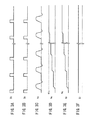
まず、トランス14の2次巻線18の両端に負荷20が正常に接続されている場合の動作(通常動作)について図3A〜図3Fを参照しながら説明する。パワーMOSFET24において1回目のターンオフが行われると、該パワーMOSFET24には、図3Cに示すように、負荷20に印加される出力電圧Vout(図2A参照)に応じた電圧Vsが印加されることになる。特に、負荷20が放電負荷の場合には、負荷インピーダンスが急激に低下し、出力電圧Voutの低下や出力電圧Voutがクランプされて負荷20が開放した状態に比べてより低い出力電圧になる場合が多い。そして、この通常動作においては、パワーMOSFET24での数回のオン動作及びオフ動作が繰り返されることで、コンデンサ42への充電が行われ、最終的にコンデンサ42の両端電圧Vcは、図3Dに示すように、実際にパワーMOSFET24にかかる電圧Vsとほぼ同じ電圧、つまり、通常動作における最大電圧(しきい値レベル)Vthとなる。この段階以降、コンデンサ42の両端電圧Vcは、そのまま保持される。
First, an operation (normal operation) when the
この通常動作では、コンデンサ42の両端電圧Vcがしきい値レベルVthで保持されることから、過電圧検出回路36におけるコンデンサ64の両端電圧Vrは規定電圧Va以下となり(図3E参照)、インバータ54からは高レベルの電圧が出力される(図3F参照)。従って、制御回路38からは、スイッチング指令信号Stの波形(図3A参照)とほぼ同じ波形の信号が出力され、結果的に、パワーMOSFET24のゲートに対して、前記スイッチング指令信号Stとほぼ同じ波形のスイッチング制御信号Sc(図3B参照)が供給されることになる。
In this normal operation, since the voltage Vc across the
次に、負荷20が電気的に開放状態である場合の動作(異常動作)について図4A〜図4Fを参照しながら説明する。負荷20が電気的に開放状態にあると、パワーMOSFET24がターンオフした時点以降において、トランス14のインダクタンスに蓄積されていたエネルギーによる電流がコンデンサ42の経路に転流することとなる。この電流の転流によって、図4Dに示すように、コンデンサ42の両端電圧Vcが上昇し、前記しきい値レベルVthを超えることになる。そして、コンデンサ42がさらに過大に充電される場合には、サージアブゾーバ46によって、スイッチ16への印加電圧Vsとコンデンサ42の両端電圧Vcが所定電圧(ツェナー電圧)Vbにクランプされ、これ以降の電圧上昇は抑えられる(図4C及び図4D参照)。
Next, an operation (abnormal operation) when the
この異常動作では、コンデンサ42の両端電圧Vcがしきい値レベルVthを超えることから、過電圧検出回路36におけるコンデンサ64の両端電圧Vrは規定電圧Vaを超えることになり(図4E参照)、インバータ54からは低レベルの電圧、すなわち、検出信号Skが出力される(図4F参照)。従って、制御回路38からは、スイッチング指令信号Stの波形(図4A参照)に関係なく、低レベルの信号が出力され、パワーMOSFET24のゲートには、低レベルのスイッチング制御信号Scが供給される(図4B参照)。つまり、パワーMOSFET24のオン動作が停止され、オフ動作が維持されることになる。
In this abnormal operation, the voltage Vc across the
この停止期間Tt中に、コンデンサ42が放電し、コンデンサ42の両端電圧Vcがしきい値レベルVthよりも低下し(図4D参照)、それに応じて第2の抵抗50の両端電圧も低下し、コンデンサ64の両端電圧も徐々に低下していくことになる(図4E参照)。
During this stop period Tt, the
第2の抵抗50に対して並列にコンデンサ64を接続していない場合は、コンデンサ42の両端電圧Vcの低下がそのまま反映された電圧が後段のインバータ54に供給されることになるが、本実施の形態のように、第2の抵抗50に対してコンデンサ64を接続することで、第2の抵抗50の両端電圧の低下がコンデンサ64の容量値によって決定される時間だけ遅延されてインバータ54に入力されることになる。すなわち、前記停止期間Ttはコンデンサ64の容量値によって決定されることとなり、コンデンサ64の容量値を任意に設定することで、停止期間Ttを自由に設定できる。
When the
従って、前記停止期間Ttが経過した後は、インバータ54から高レベルの電圧が出力され、制御回路38からは、スイッチング指令信号Stの波形とほぼ同じ波形の信号が出力される。この停止期間Ttが経過する前に、負荷20の接続が正常に行われれば、停止期間Ttの経過後に通常動作(図4A〜図4F参照)に入ることとなる。
Therefore, after the stop period Tt elapses, a high level voltage is output from the
一方、前記停止期間Ttが経過しても、負荷20が未だ電気的に開放状態であれば、パワーMOSFET24がターンオフした時点で再びコンデンサ42の両端電圧Vcがしきい値レベルVthを超え(図4D参照)、これに伴って第2の抵抗50の両端電圧Vrも規定電圧Vaを超えることから(図4E参照)、再度停止期間Ttに入る。つまり、この停止期間Ttによって、オン動作のための期間が間引きされた形となり、スイッチング制御信号Scによるオン/オフ制御のスイッチング周波数が低く抑えられることになる。
On the other hand, if the
もちろん、インバータ54の後段にアラーム回路を接続し、出力が低レベルとなった時点、すなわち、検出信号Skが出力された時点で、アラーム回路を通じてアラームを出力させ、使用者に負荷の異常を知らせるようにしてもよい。アラームとしては、光や音によるものを含む。この場合、例えば使用者によってスイッチング指令信号Stの供給が停止され、負荷20が正常に接続された段階で、再び使用者によってスイッチング指令信号Stの供給が再開されるというプロセスを踏むようにしてもよい。
Of course, an alarm circuit is connected to the subsequent stage of the
このように、実施の形態に係る高電圧パルス発生回路10においては、スナバ回路34に加わる過電圧を検出する過電圧検出回路36と、該過電圧検出回路36での過電圧の検出に基づいてパワーMOSFET24のオン動作を停止あるいはスイッチング周波数を低下させる制御回路38とを設けるようにしたので、例えば負荷20の異常状態や人為的なミスによって負荷20が電気的に開放状態になった場合、スイッチ16には一旦過電圧が加わることになるが、このとき、過電圧検出回路36によって過電圧が検出され、制御回路38を通じてスイッチ16のオン動作が停止することになる。つまり、過電圧が検出された後においては、スイッチ16のオン動作が停止することから、その後、スイッチ16に対して過電圧が加わるということがなくなる。従って、この実施の形態においては、高電圧パルス発生回路10の信頼性の向上を図ることができる。
As described above, in the high voltage
また、スナバ回路34に対する過電圧の繰り返し印加を考慮する必要がなくなることから、スナバ回路34を構成する回路素子として、電力容量の小さい回路素子を用いることが可能となる。これは、高信頼性を有する高電圧パルス発生回路10の小型化につながる。
In addition, since it is not necessary to consider the repeated application of overvoltage to the
ここで、スナバ回路34の電力容量について、過電圧検出回路36と制御回路38を設けない場合(比較例)と、本実施の形態とを比較して説明する。
Here, the power capacity of the
まず、異常動作において、1回のパワーMOSFET24のオフ動作によってスナバ回路34に加わる電力をP(J)、スイッチング周波数をf(Hz)としたとき、比較例のスナバ回路34に必要な電力容量W1は、
W1=P×f(W)
である。通常、スイッチング周波数は10(Hz)以上である。
First, in an abnormal operation, when the power applied to the
W1 = P × f (W)
It is. Usually, the switching frequency is 10 (Hz) or more.
一方、本実施の形態では、コンデンサ42での保持時間(=停止期間Tt)を1秒間としたとき、スイッチング周波数は1(Hz)となるから、この実施の形態におけるスナバ回路34の必要な電力容量W2は、
W2=P×1(W)
である。
On the other hand, in this embodiment, when the holding time (= stop period Tt) in the
W2 = P × 1 (W)
It is.
従って、本実施の形態に係る高電圧パルス発生回路10のスナバ回路34の電力容量は、比較例の電力容量の1/fで済む。
Therefore, the power capacity of the
上述の例では、スイッチ16に対して並列にスナバ回路34を接続した場合を示したが、その他、図5の変形例に係る高電圧パルス発生回路10aのように、トランス14の1次巻線32に対して並列にスナバ回路34を接続し、該スナバ回路34の後段に過電圧検出回路36と制御回路38を接続するようにしてもよい。この場合、過電圧検出回路36とスイッチ16の信号の基準となる電位レベルが異なるため、絶縁アンプ等を利用して信号の絶縁を取ることが必要となる。例えば、コンデンサ64の後段に接続されるインバータに絶縁アンプ等が介在されたインバータ68を用いることが好ましい。当然、信号間にトランスや光信号を用いる等して信号の絶縁を行ってもよい。
In the above example, the case where the
この変形例においても、上述した実施の形態と同様に、過電圧が検出された後においてスイッチ16のオン動作が停止することから、その後、スイッチ16に対して過電圧が加わるということがなくなり、高電圧パルス発生回路10aの信頼性の向上を図ることができる。
Also in this modified example, since the on-operation of the
また、スナバ回路34に対する過電圧の繰り返し印加を考慮する必要がなくなることから、電力容量の小さい回路素子を用いることが可能となり、高電圧パルス発生回路10の小型化を図ることができる。
In addition, since it is not necessary to consider the repeated application of overvoltage to the
なお、本発明に係る高電圧パルス発生回路は、上述の実施の形態に限らず、本発明の要旨を逸脱することなく、種々の構成を採り得ることはもちろんである。 The high-voltage pulse generation circuit according to the present invention is not limited to the above-described embodiment, and can of course have various configurations without departing from the gist of the present invention.
10、10a…高電圧パルス発生回路 12…直流電源
14…トランス 16…スイッチ
18…2次巻線 20…負荷
26…ゲート駆動回路 32…1次巻線
34…スナバ回路 36…過電圧検出回路
38…制御回路 42、64…コンデンサ
46…サージアブゾーバ 50…第2の抵抗
DESCRIPTION OF
Claims (4)
前記スイッチの両端に直列に接続されたスナバダイオードとスナバコンデンサと、前記スナバコンデンサに並列に接続されたサージアブゾーバからなる電圧クランプ型のスナバ回路と、
前記スナバコンデンサもしくは前記サージアブゾーバの両端から過電圧を検出する過電圧検出回路と、
前記過電圧の検出に基づいて少なくとも前記スイッチのオン動作を制御する制御回路を備えていることを特徴とする高電圧パルス発生回路。 A high-voltage pulse generation circuit having a transformer and a switch connected in series at both ends of a DC power supply, and outputs output from both ends of a secondary winding of the transformer,
A snubber circuit of a voltage clamp type comprising a snubber diode and a snubber capacitor connected in series to both ends of the switch, and a surge absorber connected in parallel to the snubber capacitor;
An overvoltage detection circuit for detecting an overvoltage from both ends of the snubber capacitor or the surge absorber;
A high voltage pulse generation circuit comprising: a control circuit that controls at least an ON operation of the switch based on detection of the overvoltage.
前記トランスの両端に直列に接続されたスナバダイオードとスナバコンデンサと、前記スナバコンデンサに並列に接続されたサージアブゾーバからなる電圧クランプ型のスナバ回路と、
前記スナバコンデンサもしくは前記サージアブゾーバの両端から過電圧を検出する過電圧検出回路と、
前記過電圧の検出に基づいて少なくとも前記スイッチのオン動作を制御する制御回路とを備えていることを特徴とする高電圧パルス発生回路。 A high-voltage pulse generation circuit having a transformer and a switch connected in series at both ends of a DC power supply, and outputs output from both ends of a secondary winding of the transformer,
A voltage clamp type snubber circuit comprising a snubber diode and a snubber capacitor connected in series to both ends of the transformer, and a surge absorber connected in parallel to the snubber capacitor;
An overvoltage detection circuit for detecting an overvoltage from both ends of the snubber capacitor or the surge absorber;
A high-voltage pulse generation circuit comprising: a control circuit that controls at least an ON operation of the switch based on detection of the overvoltage.
前記スイッチを所定のスイッチング周波数でオン/オフ制御するスイッチング制御回路を有する場合に、
前記過電圧検出回路は、前記過電圧の検出に基づいて検出信号を出力し、
前記制御回路は、前記検出信号の入力に基づいて前記スイッチング制御回路の前記スイッチング周波数を低く設定することを特徴とする高電圧パルス発生回路。 In the high voltage pulse generation circuit according to claim 1 or 2,
When having a switching control circuit for on / off control of the switch at a predetermined switching frequency,
The overvoltage detection circuit outputs a detection signal based on the detection of the overvoltage,
The control circuit sets the switching frequency of the switching control circuit to be low based on the input of the detection signal.
前記スイッチは、自己消弧型あるいは転流消弧形のデバイスを有することを特徴とする高電圧パルス発生回路。
In the high voltage pulse generation circuit according to any one of claims 1 to 3,
The switch includes a self-extinguishing type or a commutation-extinguishing type device.
Priority Applications (1)
| Application Number | Priority Date | Filing Date | Title |
|---|---|---|---|
| JP2003408771A JP4336573B2 (en) | 2003-12-08 | 2003-12-08 | High voltage pulse generator |
Applications Claiming Priority (1)
| Application Number | Priority Date | Filing Date | Title |
|---|---|---|---|
| JP2003408771A JP4336573B2 (en) | 2003-12-08 | 2003-12-08 | High voltage pulse generator |
Publications (2)
| Publication Number | Publication Date |
|---|---|
| JP2005176416A JP2005176416A (en) | 2005-06-30 |
| JP4336573B2 true JP4336573B2 (en) | 2009-09-30 |
Family
ID=34730355
Family Applications (1)
| Application Number | Title | Priority Date | Filing Date |
|---|---|---|---|
| JP2003408771A Expired - Fee Related JP4336573B2 (en) | 2003-12-08 | 2003-12-08 | High voltage pulse generator |
Country Status (1)
| Country | Link |
|---|---|
| JP (1) | JP4336573B2 (en) |
Cited By (1)
| Publication number | Priority date | Publication date | Assignee | Title |
|---|---|---|---|---|
| US10958155B2 (en) | 2018-03-22 | 2021-03-23 | Kabushiki Kaisha Toshiba | Semiconductor device, power conversion device, driving device, vehicle, and elevator |
Families Citing this family (2)
| Publication number | Priority date | Publication date | Assignee | Title |
|---|---|---|---|---|
| JP4242865B2 (en) * | 2005-12-19 | 2009-03-25 | 株式会社 電子制御国際 | High voltage pulse power supply |
| JP6602573B2 (en) * | 2015-06-30 | 2019-11-06 | ダイハツ工業株式会社 | Power supply for plasma reactor |
-
2003
- 2003-12-08 JP JP2003408771A patent/JP4336573B2/en not_active Expired - Fee Related
Cited By (1)
| Publication number | Priority date | Publication date | Assignee | Title |
|---|---|---|---|---|
| US10958155B2 (en) | 2018-03-22 | 2021-03-23 | Kabushiki Kaisha Toshiba | Semiconductor device, power conversion device, driving device, vehicle, and elevator |
Also Published As
| Publication number | Publication date |
|---|---|
| JP2005176416A (en) | 2005-06-30 |
Similar Documents
| Publication | Publication Date | Title |
|---|---|---|
| JP6402591B2 (en) | Semiconductor device | |
| US9059709B2 (en) | Gate drive circuit for transistor | |
| US7368972B2 (en) | Power transistor control device | |
| John et al. | Fast-clamped short-circuit protection of IGBT's | |
| KR102091693B1 (en) | Protection circuit, oscillation compensation circuit and power supply circuit in solid state pulse modulator | |
| JP4779549B2 (en) | A gate driving circuit of a voltage driven semiconductor element. | |
| JP6203020B2 (en) | Battery pack having charge / discharge switch circuit | |
| KR101045198B1 (en) | Power control system startup method and circuit | |
| US8503146B1 (en) | Gate driver with short-circuit protection | |
| US7548402B2 (en) | High voltage pulse generating circuit | |
| JP6767328B2 (en) | Solenoid drive circuit | |
| JP4336573B2 (en) | High voltage pulse generator | |
| JP4079561B2 (en) | Power supply for sputtering | |
| US11749983B2 (en) | Startup protection circuit, for interrupting startup of a boost DC-DC switching converter | |
| US7932710B2 (en) | Step-up circuit and step-up circuit device | |
| US20140126088A1 (en) | Protection circuit, switch control circuit, and power supply device comprising the same | |
| JP2010193649A (en) | Semiconductor switching element driving circuit | |
| JP2020195019A (en) | Gate drive circuit | |
| JP4557110B2 (en) | Switching power supply | |
| US6316907B1 (en) | Filtering and voltage raising circuit for connection between a car radio and a motor-vehicle battery | |
| EP4246789A1 (en) | Secondary-side protection and sense circuit for power converter | |
| JP2006094609A (en) | Power supply device | |
| WO2005041389A1 (en) | Pulse generator circuit | |
| JP2022181238A (en) | Active clamp circuit | |
| JPS6074679A (en) | Protection circuit for semiconductor element |
Legal Events
| Date | Code | Title | Description |
|---|---|---|---|
| A621 | Written request for application examination |
Free format text: JAPANESE INTERMEDIATE CODE: A621 Effective date: 20060825 |
|
| TRDD | Decision of grant or rejection written | ||
| A01 | Written decision to grant a patent or to grant a registration (utility model) |
Free format text: JAPANESE INTERMEDIATE CODE: A01 Effective date: 20090623 |
|
| A01 | Written decision to grant a patent or to grant a registration (utility model) |
Free format text: JAPANESE INTERMEDIATE CODE: A01 |
|
| A977 | Report on retrieval |
Free format text: JAPANESE INTERMEDIATE CODE: A971007 Effective date: 20090625 |
|
| A61 | First payment of annual fees (during grant procedure) |
Free format text: JAPANESE INTERMEDIATE CODE: A61 Effective date: 20090629 |
|
| FPAY | Renewal fee payment (event date is renewal date of database) |
Free format text: PAYMENT UNTIL: 20120703 Year of fee payment: 3 |
|
| R150 | Certificate of patent or registration of utility model |
Free format text: JAPANESE INTERMEDIATE CODE: R150 |
|
| FPAY | Renewal fee payment (event date is renewal date of database) |
Free format text: PAYMENT UNTIL: 20120703 Year of fee payment: 3 |
|
| FPAY | Renewal fee payment (event date is renewal date of database) |
Free format text: PAYMENT UNTIL: 20130703 Year of fee payment: 4 |
|
| LAPS | Cancellation because of no payment of annual fees |