JP4331069B2 - Electronic component repair device - Google Patents
Electronic component repair device Download PDFInfo
- Publication number
- JP4331069B2 JP4331069B2 JP2004222099A JP2004222099A JP4331069B2 JP 4331069 B2 JP4331069 B2 JP 4331069B2 JP 2004222099 A JP2004222099 A JP 2004222099A JP 2004222099 A JP2004222099 A JP 2004222099A JP 4331069 B2 JP4331069 B2 JP 4331069B2
- Authority
- JP
- Japan
- Prior art keywords
- electronic component
- bga
- repair device
- board
- component
- Prior art date
- Legal status (The legal status is an assumption and is not a legal conclusion. Google has not performed a legal analysis and makes no representation as to the accuracy of the status listed.)
- Expired - Fee Related
Links
Images


Landscapes
- Electric Connection Of Electric Components To Printed Circuits (AREA)
- Wire Bonding (AREA)
Description
本発明は、プリント基板に実装される電子部品のはんだ接合部を加熱溶融して電子部品の取り外しおよび再取り付けを行うリペア装置に関する。 The present invention relates to a repair device that removes and reattaches an electronic component by heating and melting a solder joint portion of the electronic component mounted on a printed circuit board.
プリント基板に実装される電子部品には、高密度実装を可能とする電子部品として、パッケージの下面側に多数のボール状の接続端子を設けたBGA[Ball Grid Array Package]が使用されている(このBGAには、接続端子のピッチを極小としたCSP[Chip Size Package]も含まれるものとする)。 BGA [Ball Grid Array Package] in which a large number of ball-shaped connection terminals are provided on the lower surface of the package is used as an electronic component that can be mounted on a printed circuit board as a high-density mounting electronic component ( This BGA includes a CSP (Chip Size Package) in which the pitch of connection terminals is minimized.
このBGAを実装したプリント基板では、BGAに故障が生じた場合や、BGAの保守、リサイクル等の理由により、BGAの交換が必要となる場合があるため、BGAをプリント基板から取り外し、再びプリント基板に取り付けるリペア技術は不可欠である。 In the printed circuit board on which the BGA is mounted, the BGA may need to be replaced due to a failure of the BGA or due to maintenance or recycling of the BGA. Repair technology to attach to is indispensable.
このBGAのリペア工程における再取り付け時の手順を図9に示す。
図9において1はプリント基板、2はこのプリント基板1に実装される電子部品であるBGAを示し、このBGA2はパッケージの下面側に、はんだ材料によりなる多数のボール状バンプ(はんだ接合部)3を接続端子として有している。
The procedure at the time of reattachment in this BGA repair process is shown in FIG.
In FIG. 9, 1 is a printed circuit board, 2 is a BGA which is an electronic component mounted on the printed
図9(A)に示すように、プリント基板1の表面には、BGA2のバンプ3の形状や配列に合わせて、接続用のパッド4が配置形成されている。そして、同図(B)に示す如くこのパッド4の上(あるいはバンプ3の先端)にフラックス又は、はんだペースト5を塗布し、それから同図(C)に示すようにBGA2をプリント基板1上に搭載した後、バンプ3を加熱して溶融させることで、はんだ付けによってパッド4と接合する。
As shown in FIG. 9A,
従来、このBGA等の電子部品のリペアに用いる装置としては、例えば下記の特許文献1〜3に記載されているように、電子部品の中央部を吸着ノズルによって吸着保持し、電子部品のはんだ接合部に熱風を吹き付けてはんだを加熱溶融させることによって電子部品の取り外しおよび再取り付けを行う装置が提案されている。
しかしながら、これら従来のリペア装置は、何れも電子部品の中央部を吸着ノズルで吸着するだけの簡単な保持構造であるため、電子部品の取り付け時には加熱によって電子部品に反りや傾きが生じ、その結果、はんだ接合部であるバンプが部分的に大きく潰れてバンプ間が短絡状態となったり、あるいはバンプの一部がパッドに接続されず未接続の状態となる等、接続不良が発生する場合が多くあった。特に前記のBGAでは、バンプとパッドの接続部が外観からチェックできないため、接続不良が生じても発見が難しいという問題がある。 However, all of these conventional repair devices have a simple holding structure in which the central part of the electronic component is simply sucked by the suction nozzle, so that the electronic component is warped or tilted by heating when the electronic component is attached. In many cases, connection failure occurs, such as bumps that are solder joints are partially crushed and the bumps are short-circuited, or some of the bumps are not connected to the pads and are not connected. there were. In particular, the above-mentioned BGA has a problem that it is difficult to find out even if a connection failure occurs because the connection part between the bump and the pad cannot be checked from the appearance.
本発明は斯かる点に鑑みてなされたもので、電子部品のはんだ接合部を加熱溶融して取り外しおよび再取り付けを行うリペア装置において、電子部品の再取り付け時の反りや傾きを抑制し、電子部品を安定して確実に実装できるリペア装置を提供することを目的とする。 The present invention has been made in view of such points, and in a repair device that removes and reattaches a solder joint portion of an electronic component by heating and melting, suppressing warping and inclination when the electronic component is reattached, An object of the present invention is to provide a repair device that can stably and reliably mount components.
上述の目的を達成するため本発明は、
プリント基板に実装される電子部品の下面側にはんだ接合部を有し、このはんだ接合部を加熱溶融して電子部品の取り外しおよび再取り付けを行うリペア装置であって、
前記はんだ接合部を溶融させるための熱風をノズルから噴射する加熱手段と、
前記電子部品の略中央部を上面側から押さえるように保持する押さえ部材と、前記電子部品の端部の下面側から保持する複数の可動アーム部材と、を有して構成される部品保持手段と、
を備え、
前記可動アーム部材の先端部は、前記電子部品の再取り付け時に前記電子部品と前記プリント基板との間に挟まれて前記電子部品の必要以上の沈み込み防止する構成としたものである。
In order to achieve the above object, the present invention
A repair device having a solder joint on the lower surface side of an electronic component mounted on a printed circuit board, and removing and reattaching the electronic component by heating and melting the solder joint,
Heating means for injecting hot air from the nozzle for melting the solder joint portion;
Component holding means comprising: a holding member that holds the substantially central portion of the electronic component so as to be pressed from the upper surface side; and a plurality of movable arm members that are held from the lower surface side of the end portion of the electronic component ; ,
With
The distal end portion of the movable arm member is sandwiched between the electronic component and the printed board when the electronic component is reinstalled, and prevents the electronic component from sinking more than necessary .
また、本発明のリペア装置では、前記可動アーム部材の先端部を、前記電子部品を上下から挟んで保持する形状としてもよい。 Moreover, in the repair apparatus of this invention, it is good also as a shape which hold | maintains the front-end | tip part of the said movable arm member on both sides of the said electronic component from the upper and lower sides.
さらに本発明のリペア装置においては、前記プリント基板を下側から支える基板支持手段を設け、前記部品保持手段と前記基板支持手段とで前記プリント基板を上下から挟み込む構造とする。 Furthermore, in the repair apparatus of the present invention, board support means for supporting the printed board from below is provided, and the printed board is sandwiched from above and below by the component holding means and the board support means.
さらに本発明のリペア装置では、前記加熱手段のノズルから噴射される熱風を、前記電子部品に均一に吹き付けるように前記部品保持手段によって誘導する構造とすることが望ましい。 Furthermore, in the repair apparatus of this invention, it is desirable to have a structure in which the hot air sprayed from the nozzle of the heating means is guided by the component holding means so as to be blown uniformly onto the electronic component.
本発明のリペア装置は、ノズルの先端部に設けた部品保持手段において、電子部品の略中央部を押さえ部材で保持すると同時に、電子部品の端部を複数の可動アーム部材で保持する構造としたことで、電子部品は反りや傾きが生じることなくしっかりと固定保持され、その状態でノズルから熱風を噴射して電子部品の再取り付け動作を行うことにより、はんだ接合部の潰れや未接続などの接続不良が発生することはなく、電子部品を安定して確実に実装することが可能となる。 The repair device of the present invention has a structure in which, in the component holding means provided at the tip portion of the nozzle, the substantially central portion of the electronic component is held by the pressing member, and at the same time, the end portion of the electronic component is held by the plurality of movable arm members. In this state, the electronic components are firmly fixed and held without warping or tilting, and in that state, hot air is sprayed from the nozzle and the electronic components are reattached. Connection failure does not occur, and electronic components can be mounted stably and reliably.
さらに本発明のリペア装置では、電子部品の再取り付け時に、電子部品とプリント基板との間に挟まれる可動アーム部材の先端部により、電子部品の必要以上の沈み込みが防止されるので、はんだ接合部の潰れをより確実に防止することができる。 Furthermore, in the repair device of the present invention, when the electronic component is reinstalled, the tip of the movable arm member sandwiched between the electronic component and the printed board prevents the electronic component from sinking more than necessary. The collapse of the part can be prevented more reliably.
また本発明のリペア装置では、可動アーム部材の先端部を、電子部品を上下から挟んで保持する形状とすることで、電子部品の固定をより確実にすることができる。 In the repair device of the present invention, the tip of the movable arm member is shaped so as to hold the electronic component from above and below, so that the electronic component can be fixed more reliably.
さらに本発明のリペア装置においては、プリント基板を下側から支える基板支持手段を設け、部品保持手段と基板支持手段とでプリント基板を上下から挟み込む構造とすることにより、プリント基板の反りも抑えることができるので、電子部品の再取り付け時の接続不良を一段と確実に防止することができる。 Further, in the repair device of the present invention, the board support means for supporting the printed board from the lower side is provided, and the printed board is sandwiched from above and below by the component holding means and the board support means, thereby suppressing the warpage of the printed board. Therefore, it is possible to more reliably prevent a connection failure when the electronic component is reattached.
さらに本発明のリペア装置では、加熱手段のノズルから噴射される熱風を、電子部品に均一に吹き付けるように部品保持手段によって誘導する構造とすることで、はんだ接合部を均一に加熱溶融させ、電子部品をより安定して確実に実装することが可能となる。 Furthermore, in the repair device of the present invention, the structure is such that the hot air sprayed from the nozzle of the heating means is guided by the component holding means so as to be blown uniformly onto the electronic component, thereby uniformly heating and melting the solder joint portion. Components can be more stably and reliably mounted.
以下、図面を参照しながら本発明の好適な実施例について詳細に説明する。
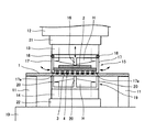
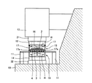
図1は、本発明によるリペア装置の主要部の構成を示す側面図である。このリペア装置は、下基部10に立設された支持台11にプリント基板1を載置固定し、このプリント基板1に対して電子部品であるBGA2の取り外しおよび取り付けを行うものである。
Hereinafter, preferred embodiments of the present invention will be described in detail with reference to the drawings.
FIG. 1 is a side view showing a configuration of a main part of a repair device according to the present invention. In this repair device, the printed
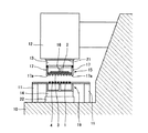
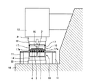
このリペア装置は、BGA2の下面側に設けられたはんだ接合部であるバンプ3を溶融させるための高温の熱風を発生させる加熱手段(図示せず)を内蔵し、この加熱手段から発せられた熱風Hが、プリント基板1の上方に配置された上基部12より突出する上側ノズル13および下基部10より突出する下側ノズル14からBGA2に向けて噴射されるようになっている。
This repair device has a built-in heating means (not shown) that generates high-temperature hot air for melting the
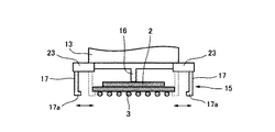
そしてこのリペア装置において上側ノズル13の先端部には、BGA2を保持するための部品保持手段15が設けられている。この部品保持手段15は、BGA2の略中央部を上面側から押さえるように保持する押さえ部材16と、BGA2の端部に係合し、BGA2を挟むように保持する複数の可動アーム部材17と、を有して構成される。
In this repair device, a component holding means 15 for holding the
可動アーム部材17は、BGA2の角部に対応して各々が軸部18を支点として開閉するように回動自在に設けられ、その先端部17aが鉤状に折曲されてBGA2の端部に係合し、BGA2を下面側から保持する構造となっている。ここで可動アーム部材17は、BGA2とプリント基板1との間に入り込む先端部17aの厚みを、バンプ3の大きさに合わせて可変調整できるものとする。このように構成される部品保持手段15は、上基部12と上側ノズル13との間に設けられた昇降機構21によって上側ノズル13と一体にプリント基板1に対し上下移動されるようになっている。
The
さらにこのリペア装置においては、下側ノズル14の先端部に、プリント基板1を下側から支える基板支持手段19が設けられている。この基板支持手段19は、前記部品保持手段15の押さえ部材16および可動アーム17と対向し、プリント基板1の下面側を支持する支持部材20を有して構成され、前記部品保持手段15とこの基板支持手段19とで上下からプリント基板1を挟み込む構造としてある。この基板支持手段19もまた前記部品保持手段15と同様に、下基部10と下側ノズル14との間に設けられた昇降機構22によって下側ノズル14と一体にプリント基板1に対し上下移動されるようになっている。
Further, in this repair device, a substrate support means 19 for supporting the printed
このリペア装置において、上下のノズル13,14、部品保持手段15および基板支持手段19は、BGA2に合わせた大きさや形状に製作するか、あるいは、BGA2に合わせて大きさや形状を変化させることのできる構造とする必要がある。また、部品保持手段15および基板支持手段19は、熱風による本来の加熱を妨げないような構成とし、その材質としては、プリント基板1やBGA2を傷付けず、かつ耐熱性が高い樹脂材を使用することが望ましい。この樹脂材としては、例えばテフロンの商標名で知られるテトラフロロエチレン樹脂が好適である。
In this repair device, the upper and
またこのリペア装置において、可動アーム部材17を開閉動作させるための駆動手段としては、手動式と電動式のどちらを採用してもよい。さらに上下のノズル13,14を上下移動させる昇降機構21,22も、手動式と電動式のどちらでもよいが、BGA2の接合時の圧力を制御できるものでなければならない。
In this repair device, either a manual type or an electric type may be adopted as a driving means for opening and closing the
以上の如く構成される本実施例のリペア装置においては、BGA2の略中央部を上面側から押さえ部材16で保持すると同時に、BGA2の端部を下面側から複数の可動アーム部材17で保持する構造としたことにより、BGA2は反りや傾きが生じることなくしっかりと部品保持手段15に固定保持される。
In the repair device of this embodiment configured as described above, the structure in which the substantially central portion of the
そしてこの部品保持手段15では、バンプ3が加熱溶融されてBGA2が沈み込む状態となっても、BGA2とプリント基板1との間に挟まれる可動アーム部材17の先端部17aの厚みよりBGA2とプリント基板1の間隔が狭くなることはなく、これによってBGA2の必要以上の沈み込みが防止される。
In this
またこのリペア装置においては、バンプ3を溶融させるための熱風をプリント基板1の上下に配置されたノズル13と14から均等に噴射するとともに、部品保持手段15と基板支持手段19とでプリント基板1を上下から挟み込む構造としたことにより、プリント基板1の反りの発生も抑制することができる。
In this repair device, hot air for melting the
さらにこのリペア装置では、上側ノズル13から噴射される熱風Hの拡散が部品保持手段15によって抑えられ、即ち可動アーム部材17が熱風HをBGA2に均一に吹き付けるように誘導する構造となっており、これによってバンプ3を均一に加熱溶融させることができる。また、下側ノズル14から噴射される熱風Hに対しても、基板支持手段19が同様に作用し、バンプ3が均一に加熱溶融される。
Furthermore, in this repair device, the diffusion of the hot air H sprayed from the
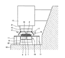
図2は、部品保持手段の他の構成例を示す。
即ちこの例の部品保持手段15は、可動アーム部材17の先端部17aを二股状に形成し、BGA2を上下から挟んで保持する形状としたものであり、これによってBGA2をより確実に固定することができる。
FIG. 2 shows another configuration example of the component holding means.
In other words, the component holding means 15 in this example is formed in a shape in which the
図3は、部品保持手段のさらに他の構成例を示す。
即ちこの例の部品保持手段15は、可動アーム部材17をスライドレール23に沿って内外方向に平行にスライドさせて開閉する構造としたものである。
FIG. 3 shows still another configuration example of the component holding means.
That is, the component holding means 15 of this example is configured to open and close by sliding the
続いて、図4〜図8を参照し、本実施例のリペア装置によるBGAの再取り付け動作について説明する。
このBGAの取り付け動作の前には、予め図9(B)に示すように、プリント基板1のパッド4上(あるいはバンプ3の先端)にフラックス又は、はんだペースト5を塗布しておく。そして先ず、図4に示すように、支持台11に載置されたプリント基板1の上方において、接合しようとするBGA2を部品保持手段15に保持させる。このとき、前述した如く部品保持手段15では、BGA2の略中央部を上面側から押さえ部材16で保持すると同時に、BGA2の端部を下面側から複数の可動アーム部材17で保持する構造により、BGA2は反りや傾きが生じることなくしっかりと固定保持される。
Next, with reference to FIGS. 4 to 8, the BGA remounting operation by the repair device of this embodiment will be described.
Prior to this BGA mounting operation, as shown in FIG. 9B, flux or
次に、この状態から昇降機構21を動作させて、図5に示すように上側ノズル14と一体に部品保持手段15を降下させ、プリント基板1上にBGA2を載せる状態とする。この状態では、基板支持手段19がプリント基板1を下側から支え、前述した如く部品保持手段15と基板支持手段19とでプリント基板1が上下から挟み込まれる状態となるので、プリント基板1の反りの発生が抑えられる。またこの状態では、後にバンプ3が溶融した時にBGA2が沈み込むことを考慮し、昇降機構18によってBGA2をプリント基板1に弱い力で押し付けるようにしておく。
Next, the
続いてこの状態から、図6のように上下のノズル13,14より熱風Hを噴射し、BGA2のバンプ3を加熱溶融させてプリント基板1のパッド4に接合する。このとき、前述したようにBGA2は、反りや傾きが生じることなくしっかりと部品保持手段15に固定保持されているので、バンプ3の潰れや未接続などの接続不良が発生することはなく、プリント基板1に対し安定して確実に接合される。また、バンプ3が溶融されてBGA2が沈み込む状態となっても、BGA2とプリント基板1との間に挟まれる可動アーム部材17の先端部17aにより、BGA2の必要以上の沈み込みが防止されるので、バンプ3の潰れをより確実に防止することができる。さらに、上下のノズル13,14から噴射された熱風Hは、部品保持手段15および基板支持手段19に誘導されてBGA2に向けて均一に吹き付けられるので、バンプ3をむらなく加熱溶融させてBGA2をより確実に接合することができる。
Subsequently, from this state, hot air H is sprayed from the upper and
こうしてプリント基板1にBGA2を接合した後、所要の冷却時間をおき、バンプ3が冷えて固まってから、図7に示すように部品保持手段15の可動アーム部材17を開き、BGA2の保持を解除する。そして最後に、図8に示す如く、昇降機構21を動作させて上側ノズル13と一体に部品保持手段15を上昇させることで、BGAの取り付け工程が完了する。なお、このBGAの取り付け完了後、基板支持手段19は図7の位置のままでも問題はないが、図8のようにこの基板支持手段19を下側ノズル14と一体に昇降機構22によって降下させることで、支持台11からプリント基板1を取り外す際に、プリント基板1の下面側に実装された部品が基板支持手段19と接触することを防止することができる。
After the
このように本実施例のリペア装置によれば、BGAの再取り付け動作を安定して行うことができ、多ピンで狭ピッチのCSPや、バンプが融点の高い鉛フリー組成のBGAにおいても確実な実装が可能である。 As described above, according to the repair device of the present embodiment, the BGA remounting operation can be performed stably, and even in a multi-pin, narrow pitch CSP and a BGA having a lead-free composition with a high melting point of the bump. Implementation is possible.
なお、BGAの取り外しについては詳細な説明を省略するが、BGAの取り外し動作は、以上の図4〜図8の取り付け動作と逆の動作によって行われることになる。 Although detailed description of the removal of the BGA is omitted, the removal operation of the BGA is performed by the reverse operation of the above-described attachment operations of FIGS.
1…プリント基板、2…BGA(電子部品)、3…バンプ(はんだ接合部)、13,14…ノズル、15…部品保持手段、16…押さえ部材、17…可動アーム部材、17a…先端部、19…基板支持手段、H…熱風
DESCRIPTION OF
Claims (4)
前記はんだ接合部を溶融させるための熱風をノズルから噴射する加熱手段と、
前記電子部品の略中央部を上面側から押さえるように保持する押さえ部材と、前記電子部品の端部を下面側から保持する複数の可動アーム部材と、を有し、前記加熱手段のノズルの先端部において前記電子部品を保持する部品保持手段と、
を備え、
前記可動アーム部材の先端部は、前記電子部品の再取り付け時に前記電子部品と前記プリント基板との間に挟まれて前記電子部品の必要以上の沈み込み防止することを特徴とする電子部品のリペア装置。 A repair device having a solder joint on the lower surface side of an electronic component mounted on a printed circuit board, and removing and reattaching the electronic component by heating and melting the solder joint,
Heating means for injecting hot air from the nozzle for melting the solder joint portion;
A pressing member that holds the substantially central portion of the electronic component from the upper surface side, and a plurality of movable arm members that hold the end portion of the electronic component from the lower surface side , and the tip of the nozzle of the heating unit Component holding means for holding the electronic component in the section;
With
The tip of the movable arm member is sandwiched between the electronic component and the printed circuit board when the electronic component is reinstalled to prevent the electronic component from sinking more than necessary. apparatus.
前記可動アーム部材の先端部を、前記電子部品を上下から挟んで保持する形状としたことを特徴とする電子部品のリペア装置。 The electronic device repair device according to claim 1 ,
An electronic component repair device characterized in that the tip of the movable arm member is shaped to hold the electronic component from above and below.
前記プリント基板を下側から支える基板支持手段を設け、前記部品保持手段と前記基板支持手段とで前記プリント基板を上下から挟み込む構造としたことを特徴とする電子部品のリペア装置。 In the repair apparatus of the electronic component of Claim 1 or 2 ,
An electronic component repair device comprising board support means for supporting the printed board from below and sandwiching the printed board from above and below by the component holding means and the board support means.
前記加熱手段のノズルから噴射される熱風を、前記電子部品に均一に吹き付けるように前記部品保持手段によって誘導する構造としたことを特徴とする電子部品のリペア装置。 In the repair apparatus of the electronic components of any one of Claims 1-3 ,
An electronic component repair device characterized in that hot air sprayed from a nozzle of the heating unit is guided by the component holding unit so as to be uniformly blown onto the electronic component.
Priority Applications (1)
| Application Number | Priority Date | Filing Date | Title |
|---|---|---|---|
| JP2004222099A JP4331069B2 (en) | 2004-07-29 | 2004-07-29 | Electronic component repair device |
Applications Claiming Priority (1)
| Application Number | Priority Date | Filing Date | Title |
|---|---|---|---|
| JP2004222099A JP4331069B2 (en) | 2004-07-29 | 2004-07-29 | Electronic component repair device |
Publications (2)
| Publication Number | Publication Date |
|---|---|
| JP2006041375A JP2006041375A (en) | 2006-02-09 |
| JP4331069B2 true JP4331069B2 (en) | 2009-09-16 |
Family
ID=35906015
Family Applications (1)
| Application Number | Title | Priority Date | Filing Date |
|---|---|---|---|
| JP2004222099A Expired - Fee Related JP4331069B2 (en) | 2004-07-29 | 2004-07-29 | Electronic component repair device |
Country Status (1)
| Country | Link |
|---|---|
| JP (1) | JP4331069B2 (en) |
Cited By (1)
| Publication number | Priority date | Publication date | Assignee | Title |
|---|---|---|---|---|
| CN108453335A (en) * | 2017-02-20 | 2018-08-28 | 迈普通信技术股份有限公司 | The anti-short-circuit support jig of BGA Rework stations, support construction and application method |
Families Citing this family (8)
| Publication number | Priority date | Publication date | Assignee | Title |
|---|---|---|---|---|
| JP4519614B2 (en) * | 2004-11-19 | 2010-08-04 | 富士通株式会社 | Circuit chip package removal jig |
| KR100847109B1 (en) * | 2006-11-14 | 2008-07-18 | 이종애 | Repairing device of Vizie package |
| JP2010161123A (en) * | 2009-01-06 | 2010-07-22 | Fujitsu Ltd | Device and method for repairing electronic component |
| JP2011211073A (en) | 2010-03-30 | 2011-10-20 | Fujitsu Ltd | Repairing device for electronic component, repairing method, and heat transfer cap member for use in repair |
| JP5505181B2 (en) * | 2010-08-06 | 2014-05-28 | 富士通株式会社 | Electronic component repair method, electronic component repair device, and heat transfer plate |
| JP5720433B2 (en) * | 2011-06-23 | 2015-05-20 | 富士通株式会社 | Surface mount type component removal method, surface mount type component removal apparatus, and semiconductor package manufacturing method |
| KR20210121770A (en) * | 2020-03-31 | 2021-10-08 | 스템코 주식회사 | Work stage unit and Reflow apparatus with the work stage unit |
| JP7566642B2 (en) * | 2021-01-06 | 2024-10-15 | キヤノンマシナリー株式会社 | Pressing device and pressing method |
-
2004
- 2004-07-29 JP JP2004222099A patent/JP4331069B2/en not_active Expired - Fee Related
Cited By (1)
| Publication number | Priority date | Publication date | Assignee | Title |
|---|---|---|---|---|
| CN108453335A (en) * | 2017-02-20 | 2018-08-28 | 迈普通信技术股份有限公司 | The anti-short-circuit support jig of BGA Rework stations, support construction and application method |
Also Published As
| Publication number | Publication date |
|---|---|
| JP2006041375A (en) | 2006-02-09 |
Similar Documents
| Publication | Publication Date | Title |
|---|---|---|
| KR20030092026A (en) | Flip chip interconnection using no-clean flux | |
| KR100368695B1 (en) | Method for mounting semiconductor elements | |
| JP2009164310A (en) | Electronic component repair device and electronic component repair method | |
| JP4331069B2 (en) | Electronic component repair device | |
| US6182884B1 (en) | Method and apparatus for reworking ceramic ball grid array or ceramic column grid array on circuit cards | |
| CN102169809B (en) | BGA component repairing method and fixture | |
| JP4696110B2 (en) | Electronic component mounting method and electronic component mounting apparatus | |
| JPH08204327A (en) | Mounting device | |
| JP2001185841A (en) | Heating and melting equipment for mounting electronic components | |
| JP4675667B2 (en) | Electronic component mounting method | |
| JP3381565B2 (en) | Bonding method of work with bump | |
| JP4260712B2 (en) | Electronic component mounting method and apparatus | |
| JP2947220B2 (en) | Flip chip connection method and flip chip mounting device | |
| JP2007059652A (en) | Electronic component mounting method | |
| JP4102538B2 (en) | Electronic circuit board repair method | |
| CN1985551B (en) | Low heat-resistant surface mounting component and mounting substrate bump-connected thereto | |
| JP2001156441A (en) | Repair method for CSP / BGA | |
| JP3235192B2 (en) | Wiring board connection method | |
| JPH0737890A (en) | Solder ball joining apparatus and joining method thereof | |
| JP3123266B2 (en) | IC removal jig and IC removal device | |
| JP4664802B2 (en) | Circuit board, circuit board manufacturing method, and electronic device | |
| JP3997614B2 (en) | Mounting soldering method | |
| US20060163330A1 (en) | Site flattening tool and method for circuit board repair | |
| JP2001119136A (en) | Method and device for smt repairing | |
| JP4569361B2 (en) | Circuit board and laser soldering method |
Legal Events
| Date | Code | Title | Description |
|---|---|---|---|
| A621 | Written request for application examination |
Free format text: JAPANESE INTERMEDIATE CODE: A621 Effective date: 20060525 |
|
| A977 | Report on retrieval |
Free format text: JAPANESE INTERMEDIATE CODE: A971007 Effective date: 20090105 |
|
| A131 | Notification of reasons for refusal |
Free format text: JAPANESE INTERMEDIATE CODE: A131 Effective date: 20090120 |
|
| A521 | Written amendment |
Free format text: JAPANESE INTERMEDIATE CODE: A523 Effective date: 20090318 |
|
| TRDD | Decision of grant or rejection written | ||
| A01 | Written decision to grant a patent or to grant a registration (utility model) |
Free format text: JAPANESE INTERMEDIATE CODE: A01 Effective date: 20090616 |
|
| A01 | Written decision to grant a patent or to grant a registration (utility model) |
Free format text: JAPANESE INTERMEDIATE CODE: A01 |
|
| A61 | First payment of annual fees (during grant procedure) |
Free format text: JAPANESE INTERMEDIATE CODE: A61 Effective date: 20090617 |
|
| R150 | Certificate of patent or registration of utility model |
Free format text: JAPANESE INTERMEDIATE CODE: R150 |
|
| FPAY | Renewal fee payment (event date is renewal date of database) |
Free format text: PAYMENT UNTIL: 20120626 Year of fee payment: 3 |
|
| FPAY | Renewal fee payment (event date is renewal date of database) |
Free format text: PAYMENT UNTIL: 20120626 Year of fee payment: 3 |
|
| FPAY | Renewal fee payment (event date is renewal date of database) |
Free format text: PAYMENT UNTIL: 20130626 Year of fee payment: 4 |
|
| LAPS | Cancellation because of no payment of annual fees |