JP4330516B2 - Semiconductor memory device - Google Patents
Semiconductor memory device Download PDFInfo
- Publication number
- JP4330516B2 JP4330516B2 JP2004310078A JP2004310078A JP4330516B2 JP 4330516 B2 JP4330516 B2 JP 4330516B2 JP 2004310078 A JP2004310078 A JP 2004310078A JP 2004310078 A JP2004310078 A JP 2004310078A JP 4330516 B2 JP4330516 B2 JP 4330516B2
- Authority
- JP
- Japan
- Prior art keywords
- memory cell
- power supply
- supply voltage
- memory device
- semiconductor memory
- Prior art date
- Legal status (The legal status is an assumption and is not a legal conclusion. Google has not performed a legal analysis and makes no representation as to the accuracy of the status listed.)
- Expired - Fee Related
Links
Images


Classifications
-
- G—PHYSICS
- G11—INFORMATION STORAGE
- G11C—STATIC STORES
- G11C11/00—Digital stores characterised by the use of particular electric or magnetic storage elements; Storage elements therefor
- G11C11/21—Digital stores characterised by the use of particular electric or magnetic storage elements; Storage elements therefor using electric elements
- G11C11/34—Digital stores characterised by the use of particular electric or magnetic storage elements; Storage elements therefor using electric elements using semiconductor devices
- G11C11/40—Digital stores characterised by the use of particular electric or magnetic storage elements; Storage elements therefor using electric elements using semiconductor devices using transistors
- G11C11/41—Digital stores characterised by the use of particular electric or magnetic storage elements; Storage elements therefor using electric elements using semiconductor devices using transistors forming static cells with positive feedback, i.e. cells not needing refreshing or charge regeneration, e.g. bistable multivibrator or Schmitt trigger
- G11C11/413—Auxiliary circuits, e.g. for addressing, decoding, driving, writing, sensing, timing or power reduction
- G11C11/417—Auxiliary circuits, e.g. for addressing, decoding, driving, writing, sensing, timing or power reduction for memory cells of the field-effect type
-
- G—PHYSICS
- G11—INFORMATION STORAGE
- G11C—STATIC STORES
- G11C2207/00—Indexing scheme relating to arrangements for writing information into, or reading information out from, a digital store
- G11C2207/22—Control and timing of internal memory operations
- G11C2207/2227—Standby or low power modes
Landscapes
- Engineering & Computer Science (AREA)
- Microelectronics & Electronic Packaging (AREA)
- Computer Hardware Design (AREA)
- Static Random-Access Memory (AREA)
- Dram (AREA)
Description
本発明は、半導体記憶装置に関し、より特定的には、メモリセルアレイ部の低消費電力化および高速化を実現する半導体記憶装置に関する。 The present invention relates to a semiconductor memory device, and more particularly to a semiconductor memory device that realizes low power consumption and high speed of a memory cell array portion.
近年、半導体集積回路では、プロセスの微細化に伴い、スタンバイ状態におけるトランジスタのリーク電流(オフリーク電流やゲートリーク電流など)の増加が問題となっている。また、近年では、SRAM、DRAM、ROM等の半導体記憶装置の容量は、飛躍的に増加している。このため、半導体集積回路では、内蔵される半導体記憶装置に含まれるメモリセルアレイの消費電力が、回路全体の消費電力のうちで大きな割合を占めるに至っている。したがって、半導体集積回路を低消費電力化するためには、半導体記憶装置に含まれるメモリセルアレイを低消費電力化することが効果的である。 In recent years, with the miniaturization of processes in semiconductor integrated circuits, an increase in transistor leakage current (off-leakage current, gate leakage current, etc.) in a standby state has become a problem. In recent years, the capacity of semiconductor memory devices such as SRAM, DRAM, and ROM has been dramatically increased. For this reason, in the semiconductor integrated circuit, the power consumption of the memory cell array included in the built-in semiconductor memory device has become a large proportion of the power consumption of the entire circuit. Therefore, in order to reduce the power consumption of the semiconductor integrated circuit, it is effective to reduce the power consumption of the memory cell array included in the semiconductor memory device.
半導体記憶装置に含まれるメモリセルアレイの低消費電力化に関する従来例としては、例えば、特許文献1に記載されている方法がある。特許文献1に記載の半導体記憶装置は、メモリセルを構成するN型MOSトランジスタの基板電極にバックバイアス電圧を供給することにより、スタンバイ時におけるサブスレッショルド電流によるリーク電流を低減する。これにより、半導体記憶装置の低消費電力化が図られる。
As a conventional example related to low power consumption of a memory cell array included in a semiconductor memory device, for example, there is a method described in
また、その他の従来例としては、特許文献2に記載されている方法がある。図17は、特許文献2に記載の半導体記憶装置の構成図である。図17に示す半導体記憶装置は、m行n列に配置された完全CMOS型のメモリセル7から構成されるメモリセルアレイ17を備える。メモリセル7は、負荷用P型MOSFET(以下、負荷用PMOSという)1および2、駆動用N型MOSFET(以下、駆動用NMOSという)3および4、並びに、転送用N型MOSFET(以下、転送用NMOSという)5および6を備える。
As another conventional example, there is a method described in
負荷用PMOS1および2のソース電極、負荷用PMOS1の基板電極15、並びに、負荷用PMOS2の基板電極16は、いずれも電源端子8(電源電圧VDD)に接続される。また、負荷用PMOS1および2のドレイン電極は、それぞれ、メモリセルの記憶ノード20および21に接続される。駆動用NMOS3の基板電極13、および、駆動用NMOS4の基板電極14は、共に接地端子9(接地電位VSS)に接続される。また、駆動用NMOS3および4のソース電極は、共にソース線23に接続され、ドレイン電極は、それぞれ、記憶ノード20および21に接続される。
The source electrodes of the
転送用NMOS5の基板電極11、および、転送用NMOS6の基板電極12は、共に接地端子9に接続される。また、転送用NMOS5および6のゲート電極は、共にワード線22に接続され、ドレイン電極はビット線18および19に、ソース電極は記憶ノード20および21にそれぞれ接続される。記憶ノード20は、負荷用PMOS2および駆動用NMOS4のゲート電極に接続され、記憶ノード21は、負荷用PMOS1および駆動用NMOS3のゲート電極に接続される。以上のように、メモリセル7内の負荷用PMOS1および2、並びに、駆動用NMOS3および4は、ラッチ回路を構成する。
The
メモリセル7には、ソース線23を介して、スイッチ回路33が接続される。スイッチ回路33の構成の説明は省略するが、以下、その動作を簡単に説明する。スイッチ回路33は、活性状態にあるメモリセル7に接続されたソース線23に対しては、接地電位VSSを供給し、非活性状態にあるメモリセル7に接続されたソース線23に対しては、電源電圧VDDと接地電位VSSとの中間電位(特許文献2の実施形態では、0.5Vに設定されている)を供給する。
A
メモリセル7が非活性状態であるときには、スイッチ回路33は、メモリセル7に接続されるソース線23の電位を上記の中間電位まで上げる。この結果、駆動用NMOS3および4の閾値電圧が基板バイアス効果により上昇し、メモリセル7からのサブスレッショルド電流によるリーク電流が低減される。特許文献2に記載の半導体記憶装置は、以上のように、スイッチ回路によって各メモリセルの駆動用NMOSのソース電位を制御することにより、消費電力を低減する。
しかしながら、上記従来の半導体記憶装置には、以下に述べるような問題がある。特許文献1および2に記載の半導体記憶装置は、いずれも基板バイアス効果によってトランジスタの閾値電圧を上げることにより、メモリセルからのリーク電流を低減する。したがって、これらの装置では、トランジスタの閾値電圧が上昇することにより、低電源電圧でのトランジスタの動作特性が悪化する。また、特許文献1に記載の半導体記憶装置においては、バックバイアス電圧を供給するための制御回路が必要であるため、回路の面積が増加するという問題がある。また、特許文献2に記載の半導体記憶装置においても、ソース線に電圧を供給するスイッチ回路が必要であるため、回路の面積が増加するという問題がある。
However, the conventional semiconductor memory device has the following problems. In each of the semiconductor memory devices described in
それ故に、本発明は、メモリセルにおけるリーク電流を効果的に抑制することにより、低電源電圧での動作特性の優れた、低消費電力、かつ、高速な半導体記憶装置を提供することを目的とする。 Therefore, an object of the present invention is to provide a low-power consumption and high-speed semiconductor memory device having excellent operation characteristics at a low power supply voltage by effectively suppressing a leakage current in a memory cell. To do.
本発明の半導体記憶装置は、ワード線と、ビット線と、電源線と、ワード線とビット線と電源線とに接続されたメモリセルとに加えて、活性なワード線に接続されたメモリセルに対しては、電源線を介して、所定の電源電圧を供給し、非活性なワード線に接続されたメモリセルに対しては、電源線を介して、所定の電源電圧よりも低く、かつ、メモリセルがデータを保持できる最低レベル以上の電圧を供給するメモリセル電源電圧制御回路とを備える。 In addition to word lines, bit lines, power supply lines, memory cells connected to word lines, bit lines, and power supply lines, the semiconductor memory device of the present invention has memory cells connected to active word lines. For a memory cell connected to an inactive word line, a predetermined power supply voltage is supplied via the power supply line, and is lower than the predetermined power supply voltage via the power supply line. And a memory cell power supply voltage control circuit for supplying a voltage of a minimum level or higher that allows the memory cell to hold data.
また、メモリセル電源電圧制御回路は、直列接続された第1〜3のトランジスタを備え、第1のトランジスタは、所定の電源電圧が印加される電源端子と第2のトランジスタとに接続され、第2のトランジスタは、第1のトランジスタと第2のトランジスタとの間にダイオード型にゲート接続され、第3のトランジスタは、第2のトランジスタと接地端子とに接続され、第1および第3のトランジスタは、外部から供給されるアドレス信号に基づいて制御される。 Further, the memory cell power supply voltage control circuit includes a first to third transistors which are serially connected, the first transistor is connected to a power supply terminal and a second transistor having a predetermined power supply voltage is applied, The second transistor is gate-connected in a diode form between the first transistor and the second transistor , the third transistor is connected to the second transistor and the ground terminal, and the first and third transistors transistors that are controlled on the basis of the address signal supplied from the outside.
また、第2のトランジスタの閾値電圧の絶対値が、メモリセルに含まれる全てのトランジスタの閾値電圧の最大値以上であることが好ましい。 The absolute value of the threshold voltage of the second transistor is preferably equal to or greater than the maximum value of the threshold voltages of all the transistors included in the memory cell.
さらに、メモリセル電源電圧制御回路は、アドレス信号が活性状態を示すときには所定の電源電圧を、アドレス信号が非活性状態を示すときには第2のトランジスタの閾値電圧を出力することが好ましい。 Further, the memory cell power supply voltage control circuit preferably outputs a predetermined power supply voltage when the address signal indicates an active state, and outputs a threshold voltage of the second transistor when the address signal indicates an inactive state.
また、メモリセル電源電圧制御回路は、ワード線が活性状態になる前に、メモリセルに所定の電源電圧を供給することが好ましい。 The memory cell power supply voltage control circuit preferably supplies a predetermined power supply voltage to the memory cell before the word line is activated.
さらに、メモリセル電源電圧制御回路は、複数のワード線に接続された複数のメモリセルに対して同じ電源電圧を供給することが好ましい。 Further, the memory cell power supply voltage control circuit preferably supplies the same power supply voltage to a plurality of memory cells connected to a plurality of word lines.
また、電源線は、メモリセルが含まれるメモリセルアレイにおける基板電位供給領域に配線され、さらに、メモリセル電源電圧制御回路は、基板電位供給領域に隣接し、かつ、ワード線ドライバ回路領域に隣接する領域に配置されることが好ましい。 The power supply line is wired to the substrate potential supply region in the memory cell array including the memory cells, and the memory cell power supply voltage control circuit is adjacent to the substrate potential supply region and adjacent to the word line driver circuit region. It is preferable to arrange in the region.
また、本発明の半導体記憶装置は、メモリセルに供給される電源電圧がメモリセルがデータを保持できる最低レベルの電圧よりも低くなることを防止するためのメモリセル電源電圧補償回路を備えることが好ましい。 The semiconductor memory device of the present invention further includes a memory cell power supply voltage compensation circuit for preventing the power supply voltage supplied to the memory cell from becoming lower than the lowest level voltage at which the memory cell can hold data. preferable.
メモリセル電源電圧補償回路は、所定の電源電圧が印加される電源端子と電源線とに接続された電荷供給素子を含んでいてもよい。 The memory cell power supply voltage compensation circuit may include a charge supply element connected to a power supply terminal to which a predetermined power supply voltage is applied and a power supply line.
また、第1のトランジスタは、メモリセル電源電圧補償回路として機能してもよい。 Further, the first transistor may function as a memory cell power supply voltage compensation circuit.
また、メモリセル電源電圧補償回路は、電源線を介してメモリセルに供給される電源電圧とこの電源電圧の基準電圧とを比較する比較回路と、この比較回路から出力される信号に応じて、所定の電源電圧が印加される電源端子と電源線とを導通および短絡するスイッチ素子とを備えることにより、メモリセルに供給される電源電圧を基準電圧以上に保持することが好ましい。 In addition, the memory cell power supply voltage compensation circuit compares a power supply voltage supplied to the memory cell via the power supply line with a reference voltage of the power supply voltage, and a signal output from the comparison circuit, It is preferable that the power supply voltage supplied to the memory cell be maintained at a reference voltage or higher by providing a switch element that conducts and short-circuits the power supply terminal to which a predetermined power supply voltage is applied and the power supply line.
さらに、比較回路およびスイッチ素子は、外部から供給されるアドレス信号が活性状態を示すときには動作を停止することが好ましい。 Furthermore, it is preferable that the comparison circuit and the switch element stop operating when an address signal supplied from the outside indicates an active state.
また、本発明の半導体記憶装置は、ビット線をプリチャージするか否かを制御する制御信号が供給されるビット線プリチャージ制御信号線と、ビット線とビット線プリチャージ制御信号線とに接続され、制御信号に基づいてビット線をプリチャージするビット線プリチャージ回路と、外部からの信号に基づいて制御信号をビット線プリチャージ制御信号線に出力するビット線プリチャージ制御回路とをさらに備え、活性なワード線が非活性な状態になる際に、ワード線に接続されたメモリセルの電源線に蓄積された電荷を、ビット線プリチャージ制御回路がビット線プリチャージ制御信号線に供給することが好ましい。 The semiconductor memory device of the present invention is connected to a bit line precharge control signal line to which a control signal for controlling whether or not to precharge the bit line is supplied, and to the bit line and the bit line precharge control signal line. A bit line precharge circuit for precharging the bit line based on the control signal; and a bit line precharge control circuit for outputting the control signal to the bit line precharge control signal line based on the signal from the outside. When the active word line becomes inactive, the bit line precharge control circuit supplies the charge accumulated in the power supply line of the memory cell connected to the word line to the bit line precharge control signal line. It is preferable.
より好ましくは、本発明の半導体記憶装置は、メモリセルの代替として使用可能な冗長救済用メモリセルと、冗長救済用メモリセルに供給される電源電圧を、メモリセル電源電圧制御回路から供給される電源電圧および接地電位のいずれかに切り替えるスイッチ素子を含む冗長救済ブロックを備えていてもよい。メモリセルの代替として使用されない冗長救済用メモリセルを含む冗長救済ブロックでは、スイッチ素子は接地電位を出力することが好ましい。 More preferably, in the semiconductor memory device of the present invention, a redundant relief memory cell that can be used as an alternative to the memory cell and a power supply voltage supplied to the redundant relief memory cell are supplied from the memory cell power supply voltage control circuit. A redundant relief block including a switch element that switches to either the power supply voltage or the ground potential may be provided. In a redundant relief block including a redundant relief memory cell that is not used as a substitute for the memory cell, the switch element preferably outputs a ground potential.
さらに、本発明の半導体記憶装置は、メモリセルの代替として使用可能な冗長救済用メモリセルと、メモリセルに供給される電源電圧を、メモリセル電源電圧制御回路から供給される電源電圧および接地電位のいずれかに切り替えるスイッチ素子とを備えていてもよい。冗長救済用メモリセルによって代替されるメモリセルでは、スイッチ素子は接地電位を出力することが好ましい。 Furthermore, the semiconductor memory device of the present invention includes a redundant relief memory cell that can be used as an alternative to a memory cell, a power supply voltage supplied to the memory cell, a power supply voltage supplied from a memory cell power supply voltage control circuit, and a ground potential. A switching element that switches to any of the above. In a memory cell replaced with a redundant relief memory cell, the switch element preferably outputs a ground potential.
本発明の半導体記憶装置は、活性なワード線に接続されたメモリセルに対しては、電源線を介して、所定の電源電圧を供給し、非活性なワード線に接続されたメモリセルに対しては、電源線を介して、所定の電源電圧よりも低く、かつ、メモリセルがデータを保持できる最低レベル以上の電圧を供給するメモリセル電源電圧制御回路を備える。したがって、本発明の半導体記憶装置は、メモリセルに記憶されるデータを正常に保持することが可能な限界の電圧(メモリセル保持電圧)まで、メモリセルに供給する電源電圧を低下させることができる。これにより、本発明の半導体記憶装置は、メモリセルからのリーク電流を低減し、半導体記憶装置の低消費電力化を実現する。また、本発明の半導体記憶装置は、メモリセルからのリーク電流を低減することにより、メモリセルからビット線に流れ出すリーク電流、あるいは、ビット線からメモリセルに流れ込むリーク電流を低減し、半導体記憶装置の書き込みおよび読み出し動作の高速化を実現する。さらに、本発明の半導体記憶装置は、従来の半導体記憶装置のように、基板バイアス効果によって閾値電圧を上昇させないことから、従来の半導体記憶装置と比較して、低電源電圧での動作性に優れている。 The semiconductor memory device of the present invention supplies a predetermined power supply voltage to the memory cells connected to the active word line via the power supply line, and to the memory cells connected to the inactive word line. The memory cell power supply voltage control circuit supplies a voltage lower than a predetermined power supply voltage and higher than a minimum level at which the memory cell can hold data via a power supply line. Therefore, the semiconductor memory device of the present invention can reduce the power supply voltage supplied to the memory cell to the limit voltage (memory cell holding voltage) at which data stored in the memory cell can be normally held. . As a result, the semiconductor memory device of the present invention reduces the leakage current from the memory cell and realizes low power consumption of the semiconductor memory device. Further, the semiconductor memory device of the present invention reduces the leakage current flowing from the memory cell to the bit line or the leakage current flowing from the bit line to the memory cell by reducing the leakage current from the memory cell. Speeding up writing and reading operations. Furthermore, unlike the conventional semiconductor memory device, the semiconductor memory device according to the present invention does not increase the threshold voltage due to the substrate bias effect, and therefore has superior operability at a low power supply voltage compared to the conventional semiconductor memory device. ing.
メモリセル電源電圧制御回路は、直列接続された第1〜3のトランジスタを備えており、第1のトランジスタが所定の電源電圧が印加される電源端子と第2のトランジスタとに接続され、第2のトランジスタが第1のトランジスタと第2のトランジスタとの間にダイオード型にゲート接続され、第3のトランジスタが第2のトランジスタと接地端子とに接続され、第1および第3のトランジスタが外部から供給されるアドレス信号に基づいて制御されるといった構成を有する。したがって、メモリセル電源電圧制御回路は、所定の電源電圧および第2のトランジスタの閾値電圧のいずれかを、ワード線の状態(活性あるいは非活性)に応じて、メモリセルに対して供給することが可能である。 Memory cell power supply voltage control circuit includes a first to third transistors which are serially connected, the first transistor is connected to a power supply terminal and a second transistor having a predetermined power supply voltage is applied, the The second transistor is gate-connected in a diode form between the first transistor and the second transistor , the third transistor is connected to the second transistor and the ground terminal, and the first and third transistors are externally connected. It is configured to be controlled based on an address signal supplied from. Therefore, the memory cell power supply voltage control circuit supplies either the predetermined power supply voltage or the threshold voltage of the second transistor to the memory cell according to the state (active or inactive) of the word line. Is possible.
また、メモリセル電源電圧制御回路に含まれる第2のトランジスタの閾値電圧の絶対値は、メモリセルに含まれる全てのトランジスタの閾値電圧の最大値以上であり、さらに、メモリセル電源電圧制御回路は、アドレス信号が活性状態を示すときには所定の電源電圧を、アドレス信号が非活性状態を示すときには第2のトランジスタの閾値電圧を出力する。これにより、メモリセル電源電圧制御回路は、周辺回路に含まれるトランジスタの特性とメモリセルに含まれるトランジスタの特性とが異なる場合においても、メモリセルに対してメモリセル保持電圧を供給することができる。 Further, the absolute value of the threshold voltage of the second transistor included in the memory cell power supply voltage control circuit is equal to or greater than the maximum value of the threshold voltage of all transistors included in the memory cell. A predetermined power supply voltage is output when the address signal indicates an active state, and a threshold voltage of the second transistor is output when the address signal indicates an inactive state. Thus, the memory cell power supply voltage control circuit can supply the memory cell holding voltage to the memory cell even when the characteristics of the transistors included in the peripheral circuit and the characteristics of the transistors included in the memory cell are different. .
また、メモリセル電源電圧制御回路は、ワード線が活性状態になる前に、メモリセルに所定の電源電圧を供給する。すなわち、メモリセルに供給される電源が確実に復帰した後にワード線が活性化する。これにより、半導体記憶装置の高速な読み出しおよび書き込み動作が実現される。 The memory cell power supply voltage control circuit supplies a predetermined power supply voltage to the memory cell before the word line is activated. That is, the word line is activated after the power supplied to the memory cell is reliably restored. Thereby, high-speed read and write operations of the semiconductor memory device are realized.
また、メモリセル電源電圧制御回路は、複数のワード線に接続された複数のメモリセルに対して同じ電源電圧を供給する。また、メモリセル電源電圧制御回路に接続される電源線は、メモリセルが含まれるメモリセルアレイにおける基板電位供給領域に配線され、メモリセル電源電圧制御回路は、基板電位供給領域に隣接し、かつ、ワード線ドライバ回路領域に隣接する領域に配置される。これにより、メモリセル電源電圧制御回路が付加されることによる半導体記憶装置の面積の増加を抑えることができる。 The memory cell power supply voltage control circuit supplies the same power supply voltage to a plurality of memory cells connected to a plurality of word lines. The power supply line connected to the memory cell power supply voltage control circuit is wired to the substrate potential supply region in the memory cell array including the memory cell, the memory cell power supply voltage control circuit is adjacent to the substrate potential supply region, and Arranged in a region adjacent to the word line driver circuit region. Thus, an increase in the area of the semiconductor memory device due to the addition of the memory cell power supply voltage control circuit can be suppressed.
また、本発明の半導体記憶装置は、メモリセルに供給される電源電圧がメモリセルがデータを保持できる最低レベルの電圧よりも低くなることを防止するためのメモリセル電源電圧補償回路を備える。このメモリセル電源電圧補償回路は、所定の電源電圧が印加される電源端子と電源線とに接続された電荷供給素子を含むことにより、メモリセルからのリーク電流による電源電圧の低下を防止する。これにより、非活性なワード線に接続されるメモリセルに対して、常に安定したメモリセル保持電圧が供給される。 The semiconductor memory device of the present invention further includes a memory cell power supply voltage compensation circuit for preventing the power supply voltage supplied to the memory cell from becoming lower than the lowest level voltage at which the memory cell can hold data. The memory cell power supply voltage compensation circuit includes a charge supply element connected to a power supply terminal to which a predetermined power supply voltage is applied and a power supply line, thereby preventing a decrease in power supply voltage due to a leak current from the memory cell. Accordingly, a stable memory cell holding voltage is always supplied to the memory cells connected to the inactive word line.
また、本発明の半導体記憶装置は、メモリセル電源電圧制御回路に含まれる第1のトランジスタをメモリセル電源電圧補償回路として使用することも可能である。これにより、メモリセル電源電圧補償回路を付加することによる半導体記憶装置の面積の増加を防ぐことができる。 In the semiconductor memory device of the present invention, the first transistor included in the memory cell power supply voltage control circuit can also be used as a memory cell power supply voltage compensation circuit. Thus, an increase in the area of the semiconductor memory device due to the addition of the memory cell power supply voltage compensation circuit can be prevented.
また、メモリセル電源電圧補償回路は、電源線を介してメモリセルに供給される電源電圧とこの電源電圧の基準電圧とを比較する比較回路と、この比較回路から出力される信号に応じて、所定の電源電圧が印加される電源端子と電源線とを導通および短絡するスイッチ素子とを備えることにより、メモリセルに供給される電源電圧を基準電圧以上に保持する。これにより、非活性なワード線に接続されるメモリセルに対して、常に安定したメモリセル保持電圧を供給することができる。 In addition, the memory cell power supply voltage compensation circuit compares a power supply voltage supplied to the memory cell via the power supply line with a reference voltage of the power supply voltage, and a signal output from the comparison circuit, By providing a power supply terminal to which a predetermined power supply voltage is applied and a switch element that conducts and short-circuits the power supply line, the power supply voltage supplied to the memory cell is held at or above the reference voltage. Thereby, a stable memory cell holding voltage can be always supplied to the memory cells connected to the inactive word line.
さらに、比較回路およびスイッチ素子は、外部から供給されるアドレス信号が活性状態を示すときには動作を停止する。これにより、ワード線が非活性な場合には、比較回路で消費される電力が削減でき、半導体記憶装置の低消費電力化が実現される。 Further, the comparison circuit and the switch element stop operating when an address signal supplied from the outside indicates an active state. Thereby, when the word line is inactive, the power consumed by the comparison circuit can be reduced, and the power consumption of the semiconductor memory device can be reduced.
また、本発明の半導体記憶装置は、ビット線をプリチャージするか否かを制御する制御信号が供給されるビット線プリチャージ制御信号線と、ビット線とビット線プリチャージ制御信号線とに接続され、制御信号に基づいてビット線をプリチャージするビット線プリチャージ回路と、外部からの信号に基づいて制御信号をビット線プリチャージ制御信号線に出力するビット線プリチャージ制御回路とをさらに備え、活性なワード線が非活性な状態になる際に、ワード線に接続されたメモリセルの電源線に蓄積された電荷を、ビット線プリチャージ制御回路がビット線プリチャージ制御信号線に供給する。これにより、電源線に蓄積された電荷が再利用されることから、半導体記憶装置の低消費電力化が実現される。 The semiconductor memory device of the present invention is connected to a bit line precharge control signal line to which a control signal for controlling whether or not to precharge the bit line is supplied, and to the bit line and the bit line precharge control signal line. A bit line precharge circuit for precharging the bit line based on the control signal; and a bit line precharge control circuit for outputting the control signal to the bit line precharge control signal line based on the signal from the outside. When the active word line becomes inactive, the bit line precharge control circuit supplies the charge accumulated in the power supply line of the memory cell connected to the word line to the bit line precharge control signal line. . As a result, the charge accumulated in the power supply line is reused, so that the power consumption of the semiconductor memory device can be reduced.
本発明の半導体記憶装置は、メモリセルの代替として使用可能な冗長救済用メモリセルと、冗長救済用メモリセルに供給される電源電圧を、メモリセル電源電圧制御回路から供給される電源電圧および接地電位のいずれかに切り替えるスイッチ素子を含む冗長救済ブロックをさらに備える。また、メモリセルの代替として使用されない冗長救済用メモリセルを含む冗長救済ブロックでは、スイッチ素子は接地電位を出力する。これにより、冗長救済ブロックに含まれるメモリセルのリーク電流を削減することができ、半導体記憶装置の低消費電力化が実現される。 A semiconductor memory device according to the present invention includes a redundant relief memory cell that can be used as an alternative to a memory cell, a power supply voltage supplied to the redundant relief memory cell, a power supply voltage supplied from a memory cell power supply voltage control circuit, and a ground A redundant relief block including a switch element that switches to one of the potentials is further provided. In the redundant relief block including the redundant relief memory cell that is not used as a substitute for the memory cell, the switch element outputs the ground potential. Thereby, the leakage current of the memory cells included in the redundant relief block can be reduced, and the power consumption of the semiconductor memory device can be reduced.
さらに、本発明の半導体記憶装置は、メモリセルの代替として使用可能な冗長救済用メモリセルと、メモリセルに供給される電源電圧を、メモリセル電源電圧制御回路から供給される電源電圧および接地電位のいずれかに切り替えるスイッチ素子とを備える。また、冗長救済用メモリセルによって代替されるメモリセルでは、スイッチ素子は接地電位を出力する。これにより、冗長救済ブロックによって置換されるメモリセルアレイのリーク電流が削減でき、半導体記憶装置の低消費電力化が実現される。 Furthermore, the semiconductor memory device of the present invention includes a redundant relief memory cell that can be used as an alternative to a memory cell, a power supply voltage supplied to the memory cell, a power supply voltage supplied from a memory cell power supply voltage control circuit, and a ground potential. A switching element for switching to any of the above. In the memory cell replaced by the redundant relief memory cell, the switch element outputs the ground potential. As a result, the leakage current of the memory cell array replaced by the redundant relief block can be reduced, and the power consumption of the semiconductor memory device can be reduced.
(第1の実施形態)
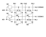
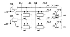
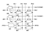
図1は、本発明の第1の実施形態に係る半導体記憶装置の構成図である。図1に示す半導体記憶装置は、メモリセル100、ワード線ドライバ回路101、メモリセル電源電圧制御回路102、ワード線WL1およびWL2、ビット線BL1、BL2、/BL1および/BL2、並びに、電源線VL1およびVL2を備える。メモリセル100は、ワード線WL1(またはWL2)、ビット線BL1および/BL1(またはBL2および/BL2)、並びに、電源線VL1(またはVL2)に接続される。
(First embodiment)
FIG. 1 is a configuration diagram of a semiconductor memory device according to the first embodiment of the present invention. The semiconductor memory device shown in FIG. 1 includes a
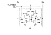
次に、図2を参照しながらメモリセル100の構成を説明する。図2に示すメモリセル100は、P型MOSトランジスタQP1およびQP2、並びに、N型MOSトランジスタQN1〜QN4を備える。P型MOSトランジスタQP1およびQP2のソース電極は、いずれも電源線VLに接続される。また、P型MOSトランジスタQP1およびQP2のドレイン電極は、それぞれ、メモリセルの記憶ノードN1およびN2に接続される。P型MOSトランジスタQP1およびQP2のソース電極には、電源線VLを介して、メモリセル電源電圧制御回路102からメモリセル電源電圧VDDMが供給される。
Next, the configuration of the
N型MOSトランジスタQN3およびQN4のソース電極は共に接地される。N型MOSトランジスタQN3およびQN4のドレイン電極は、それぞれ、記憶ノードN1およびN2に接続される。 The source electrodes of N-type MOS transistors QN3 and QN4 are both grounded. The drain electrodes of N-type MOS transistors QN3 and QN4 are connected to storage nodes N1 and N2, respectively.
N型MOSトランジスタQN1およびQN2のソース電極は、それぞれ、記憶ノードN1およびN2接続される。N型MOSトランジスタQN1およびQN2のゲート電極は、共にワード線WLに接続される。N型MOSトランジスタQN1のドレイン電極は、ビット線BLに接続され、N型MOSトランジスタQN2のドレイン電極は、ビット線/BLに接続される。N型MOSトランジスタQN1およびQN2のゲート電極には、ワード線WLを介して、ワード線ドライバ回路101からアドレス信号ADが入力される。
The source electrodes of N-type MOS transistors QN1 and QN2 are connected to storage nodes N1 and N2, respectively. The gate electrodes of N-type MOS transistors QN1 and QN2 are both connected to word line WL. The drain electrode of N-type MOS transistor QN1 is connected to bit line BL, and the drain electrode of N-type MOS transistor QN2 is connected to bit line / BL. The address signal AD from the word
記憶ノードN1は、P型MOSトランジスタQP2およびN型MOSトランジスタQN4のゲート電極に接続され、記憶ノードN2は、P型MOSトランジスタQP1およびN型MOSトランジスタQN3のゲート電極に接続される。以上のように、メモリセル100内のP型MOSトランジスタQP1およびQP2、並びに、N型MOSトランジスタQN3およびQN4は、ラッチ回路を構成する。
Storage node N1 is connected to the gate electrodes of P-type MOS transistor QP2 and N-type MOS transistor QN4, and storage node N2 is connected to the gate electrodes of P-type MOS transistor QP1 and N-type MOS transistor QN3. As described above, P-type MOS transistors QP1 and QP2 and N-type MOS transistors QN3 and QN4 in
このラッチ回路は、データを記憶し保持する。メモリセル100は、ワード線がHレベルの時にデータの読み出し、または、書き込みを行う。データの読み出しとは、ラッチ回路に記憶したデータを、ビット線BLおよび/BLに出力することであり、データの書き込みとは、ビット線BLおよび/BLを介して伝送された相補のデータを、ラッチ回路に入力し記憶することである。また、メモリセル100は、ワード線がLレベルの時には、データの読み出し、および、書き込みを行わず、ラッチ回路に記憶されたデータを保持する。
This latch circuit stores and holds data. The
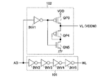
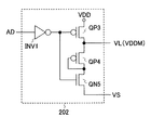
次に、図3を参照しながらメモリセル電源電圧制御回路102の構成を説明する。図3に示すメモリセル電源電圧制御回路102は、インバータINV1、P型MOSトランジスタQP3およびQP4、並びに、N型MOSトランジスタQN5を備える。メモリセル電源電圧制御回路102は、メモリセルが接続されるワード線の状態(活性あるいは非活性)に応じて、メモリセルに供給する電源電圧を制御する回路である。
Next, the configuration of the memory cell power supply
P型MOSトランジスタQP3のソース電極は、電源端子VDDに接続され、ドレイン電極は、電源線VLおよびP型MOSトランジスタQP4のソース電極に接続され、ゲート電極は、インバータINV1の出力に接続される。P型MOSトランジスタQP4は、P型MOSトランジスタQP3とN型MOSトランジスタQN5との間に、ダイオード型にゲート接続される。すなわち、P型MOSトランジスタQP4のゲート電極およびドレイン電極は、N型MOSトランジスタQN5のドレイン電極に接続され、P型MOSトランジスタQP4のソース電極は、P型MOSトランジスタQP3のドレイン電極および電源線VLに接続される。N型MOSトランジスタQN5のゲート電極は、インバータINV1の出力に接続され、また、ソース電極は接地される。 The source electrode of the P-type MOS transistor QP3 is connected to the power supply terminal VDD, the drain electrode is connected to the power supply line VL and the source electrode of the P-type MOS transistor QP4, and the gate electrode is connected to the output of the inverter INV1. The P-type MOS transistor QP4 is gate-connected in a diode form between the P-type MOS transistor QP3 and the N-type MOS transistor QN5. That is, the gate electrode and drain electrode of P-type MOS transistor QP4 are connected to the drain electrode of N-type MOS transistor QN5, and the source electrode of P-type MOS transistor QP4 is connected to the drain electrode of P-type MOS transistor QP3 and power supply line VL. Connected. The gate electrode of N-type MOS transistor QN5 is connected to the output of inverter INV1, and the source electrode is grounded.
次に、図3を参照しながらメモリセル電源電圧制御回路102の動作を説明する。インバータINV1にHレベルのアドレス信号ADが入力された場合は、P型MOSトランジスタQP3のゲート電極、および、N型MOSトランジスタQN5のゲート電極は、Lレベルとなる。この結果、P型MOSトランジスタQP3はオンになり、N型MOSトランジスタQN5はオフになるため、電源電圧VDDがメモリセル電源電圧VDDMとして、メモリセル電源電圧制御回路102から出力される。
Next, the operation of the memory cell power supply
これに対して、インバータINV1にLレベルのアドレス信号ADが入力された場合は、P型MOSトランジスタQP3のゲート電極、および、N型MOSトランジスタQN5のゲート電極は、Hレベルとなる。この結果、P型MOSトランジスタQP3はオフになり、N型MOSトランジスタQN5はオンになる。この場合、電源線VLの電位は、ダイオード型に接続されたP型MOSトランジスタQP4の閾値電圧の絶対値(以下、VTPという)になり、P型MOSトランジスタQP4の閾値電圧の絶対値VTP(<VDD)が、メモリセル電源電圧VDDMとして、メモリセル電源電圧制御回路102から出力される。
In contrast, when L-level address signal AD is input to inverter INV1, the gate electrode of P-type MOS transistor QP3 and the gate electrode of N-type MOS transistor QN5 are at H level. As a result, the P-type MOS transistor QP3 is turned off and the N-type MOS transistor QN5 is turned on. In this case, the potential of the power supply line VL becomes the absolute value of the threshold voltage (hereinafter referred to as VTP) of the P-type MOS transistor QP4 connected in a diode form, and the absolute value VTP of the threshold voltage of the P-type MOS transistor QP4 (< VDD) is output from the memory cell power supply
次に、図1に示す本実施形態に係る半導体記憶装置の動作について説明する。例えば、図1において、Hレベルのアドレス信号AD1がワード線WL1に入力されたとすると、ワード線WL1は活性状態になり、ワード線WL1に接続されたメモリセル100は活性状態になる。この場合、ワード線WL1に接続されたメモリセルに供給されるメモリセル電源電圧VDDM1は、上述したように電源電圧VDDになる。このとき、Lレベルのアドレス信号AD2が、ワード線WL2に入力されたとすると、ワード線WL2は非活性状態になり、ワード線WL2に接続されたメモリセル100は非活性状態になる。この場合、ワード線WL2に接続されたメモリセルに供給されるメモリセル電源電圧VDDM2はVTPになる。
Next, the operation of the semiconductor memory device according to this embodiment shown in FIG. 1 will be described. For example, in FIG. 1, when an H-level address signal AD1 is input to the word line WL1, the word line WL1 is activated, and the
従来の半導体記憶装置では、ワード線が活性状態あるいは非活性状態にかかわらず、メモリセル電源電圧が電源電圧VDDであるのに対して、本実施形態に係る半導体記憶装置は、上記のワード線WL2に接続されたメモリセルのように、非活性なワード線に接続されたメモリセルのメモリセル電源電圧をVTPまで下げる。本実施形態に係る半導体記憶装置は、非活性なワード線に接続されたメモリセルに供給されるメモリセル電源電圧を低くすることにより、メモリセルからのリーク電流を低減する。 In the conventional semiconductor memory device, the memory cell power supply voltage is the power supply voltage VDD regardless of whether the word line is in an active state or an inactive state. On the other hand, in the semiconductor memory device according to the present embodiment, the word line WL2 Like the memory cell connected to, the memory cell power supply voltage of the memory cell connected to the inactive word line is lowered to VTP. The semiconductor memory device according to the present embodiment reduces the leakage current from the memory cell by lowering the memory cell power supply voltage supplied to the memory cell connected to the inactive word line.
しかし、メモリセル電源電圧を低くしすぎると、メモリセルに記憶されたデータが消去されてしまうため、メモリセル電源電圧は、メモリセルが正常にデータを保持する電圧に保たれていなければならない。以下、図2を参照しながら、本実施形態に係る半導体記憶装置によれば、メモリセル電源電圧VDDMを電源電圧VDDからVTPまで下げることによって、メモリセルに記憶されたデータを正常に保持しつつ、リーク電流を低減することが可能であることを説明する。 However, if the memory cell power supply voltage is set too low, the data stored in the memory cell is erased. Therefore, the memory cell power supply voltage must be kept at a voltage at which the memory cell normally holds data. Hereinafter, referring to FIG. 2, according to the semiconductor memory device of this embodiment, the memory cell power supply voltage VDDM is lowered from the power supply voltage VDD to VTP, so that the data stored in the memory cell is normally held. It will be explained that the leakage current can be reduced.
図2に示すメモリセル100には、P型MOSトランジスタQP1およびQP2、並びに、N型MOSトランジスタQN3およびQN4によって構成されるラッチ回路が含まれる。このラッチ回路はデータを記憶する。データが正常に保持されるためには、ラッチ回路が正常に動作していればよく、ラッチ回路が正常に動作するためには、P型MOSトランジスタQP1およびQP2の一方、および、N型MOSトランジスタQN3およびQN4の一方がオン状態であれば良い。したがって、これらMOSトランジスタに供給される電圧は、ラッチ回路が正常に動作する限界の電圧(以下、メモリセル保持電圧という)まで下げることが可能である。
メモリセル100に含まれる、2つのP型MOSトランジスタQP1およびQP2が同一サイズであり、かつ、2つのN型MOSトランジスタQN3およびQN4が同一サイズである場合には、P型MOSトランジスタQP1およびQP2の閾値電圧の絶対値VTP、並びに、N型MOSトランジスタQN3およびQN4の閾値電圧(以下、VTNという)のうち高い方の電圧が、メモリセル保持電圧になる。これらのトランジスタが構成するラッチ回路は、VTPおよびVTNのいずれかの高い方の電圧がメモリセル電源電圧VDDMとしてメモリセル100に供給されていれば正常に動作する。本実施形態に係る半導体記憶装置では、VTPの絶対値がVTNよりも大きいと仮定した。したがって、本実施形態に係る半導体記憶装置は、メモリセル電源電圧VDDMがVTPの状態で、データを正常に保持する。
When two P-type MOS transistors QP1 and QP2 included in
リーク電流は、メモリセルに供給されるメモリセル電源電圧に応じて増減することから、本実施形態に係る半導体記憶装置は、メモリセル電源電圧を通常の電源電圧VDDからVTPに下げることにより、リーク電流を低減する。 Since the leakage current increases / decreases according to the memory cell power supply voltage supplied to the memory cell, the semiconductor memory device according to the present embodiment reduces the leakage current by reducing the memory cell power supply voltage from the normal power supply voltage VDD to VTP. Reduce current.
130nmプロセスの半導体記憶装置の実験では、N型MOSトランジスタの閾値電圧VTNが0.30V、P型MOSトランジスタの閾値電圧VTPが0.32Vの場合には、メモリセル電源電圧が少なくとも0.30V前後であれば、メモリセル内のデータが正常に保持されることが確認された。 In a 130 nm process semiconductor memory device experiment, when the threshold voltage VTN of the N-type MOS transistor is 0.30 V and the threshold voltage VTP of the P-type MOS transistor is 0.32 V, the memory cell power supply voltage is at least about 0.30 V Then, it was confirmed that the data in the memory cell is normally held.
以上のように、本実施形態に係る半導体記憶装置は、非活性なワード線に接続されたメモリセルに供給されるメモリセル電源電圧を、トランジスタの閾値電圧VTPまで下げることにより、メモリセルのリーク電流による消費電力を低減する。これにより、半導体記憶装置の低消費電力化が可能になる。また、本実施形態に係る半導体記憶装置は、従来の半導体記憶装置のように、基板バイアス効果によってトランジスタの閾値電圧を上げないことから、低電源電圧での動作特性が優れている。 As described above, the semiconductor memory device according to the present embodiment reduces the memory cell leakage voltage by reducing the memory cell power supply voltage supplied to the memory cells connected to the inactive word line to the threshold voltage VTP of the transistor. Reduces power consumption due to current. Thereby, the power consumption of the semiconductor memory device can be reduced. Further, unlike the conventional semiconductor memory device, the semiconductor memory device according to the present embodiment does not increase the threshold voltage of the transistor due to the substrate bias effect, and therefore has excellent operating characteristics at a low power supply voltage.
また、リーク電流は、半導体記憶装置の動作速度にも影響を与える。特に、メモリセルから流れ出るリーク電流や、メモリセルに流れ込むリーク電流は、メモリセルの読み出し時や書き込み時に弊害になる。したがって、メモリセルからビット線に流れ出すリーク電流、および、ビット線からメモリセルに流れ込むリーク電流を低減することは、半導体記憶装置の高速化を可能にする。 In addition, the leakage current also affects the operation speed of the semiconductor memory device. In particular, the leak current flowing out from the memory cell and the leak current flowing into the memory cell are harmful when the memory cell is read or written. Therefore, reducing the leakage current that flows from the memory cell to the bit line and the leakage current that flows from the bit line to the memory cell can increase the speed of the semiconductor memory device.
例えば、図2のメモリセル100からHレベルのデータ(ノードN1にHレベル、ノードN2にLレベルが記憶されている)が読み出される場合には、メモリセル100と同一ビット線上に接続された、Lレベルのデータ(ノードN1にLレベル、ノードN2にHレベルが記憶されている)が記憶されているメモリセルからのリーク電流は、メモリセル100の読み出し動作を妨害し、読み出し速度を遅くする原因になる。また、メモリセル100に対して、Hレベルのデータが書き込まれる場合も同様に、メモリセル100と同一ビット線上に接続された、Lレベルのデータが記憶されているメモリセルからのリーク電流は、メモリセル100の書き込み動作を妨害し、書き込み速度を遅くする原因になる。
For example, when H level data (H level is stored in the node N1 and L level is stored in the node N2) is read from the
本実施形態に係る半導体記憶装置は、非活性なワード線に接続されたメモリセルに供給されるメモリセル電源電圧を、トランジスタの閾値電圧VTPまで下げることによって、非活性なメモリセルからビット線に流れ出るリーク電流を低減する。これにより、リーク電流によるメモリセルの読み出しおよび書き込みの妨害が抑えられることから、本実施形態に係る半導体記憶装置によれば、読み出しおよび書き込み速度の高速化が可能となる。 In the semiconductor memory device according to this embodiment, the memory cell power supply voltage supplied to the memory cell connected to the inactive word line is lowered to the threshold voltage VTP of the transistor, so that the inactive memory cell is changed to the bit line. Reduces leakage current. As a result, the disturbance of reading and writing of the memory cell due to the leak current can be suppressed, so that the reading and writing speed can be increased according to the semiconductor memory device according to the present embodiment.
また、半導体記憶装置の読み出しおよび書き込みを高速に行うためには、メモリセル100が活性状態になる前に、メモリセル電源電圧VDDMがメモリ保持電圧VTPから電源電圧VDDに切り替わることが必要である。本実施形態に係る半導体記憶装置は、ワード線ドライバ回路101を用いて、外部からのアドレス信号ADを遅延させることにより、メモリセル100が活性状態になる前に、メモリセル電源電圧VDDMをメモリ保持電圧VTPから電源電圧VDDに切り替える。以下、図4を参照してアドレス信号ADを遅延させる方法を説明する。
Further, in order to perform reading and writing of the semiconductor memory device at high speed, it is necessary that the memory cell power supply voltage VDDM is switched from the memory holding voltage VTP to the power supply voltage VDD before the
図4は、ワード線ドライバ回路101の構成と、メモリセル電源電圧制御回路102とを示す図である。ワード線ドライバ回路101は、インバータINV2〜INV5を備える。図4に示すように、メモリセル電源電圧制御回路102では、入力から出力までのゲート段数が2段であるのに対して、ワード線ドライバ回路101では、入力から出力までのゲート段数が4段になっている。したがって、アドレス信号ADが同時にワード線ドライバ回路101とメモリセル電源電圧制御回路102とに入力されると、ワード線ドライバ回路101から出力される信号は、ゲートの段数の違いから、メモリセル電源電圧制御回路102から出力される信号に対して遅延する。
FIG. 4 is a diagram showing the configuration of the word
このように、本実施形態に係る半導体記憶装置は、ワード線ドライバ回路101を用いて、アドレス信号ADを遅延させ、メモリセル電源電圧が電源電圧VDDに確実に切り替わった後、メモリセルを活性化する。これにより、メモリセルの読み出し動作および書き込み動作の高速化を可能にする。
As described above, the semiconductor memory device according to the present embodiment uses the word
近年の半導体記憶装置では、メモリセルアレイ以外の周辺回路に含まれるトランジスタの閾値電圧と比較して、メモリセルアレイに含まれるトランジスタの閾値電圧の絶対値が高く設定される場合がある。これは、プロセスの微細化に伴い増加するトランジスタのリーク電流を低減し、半導体記憶装置の消費電力を抑えるためである。特に、大容量のメモリセルアレイを搭載した半導体記憶装置では、メモリセルアレイで消費される電力が半導体記憶装置全体の消費電力の大部分を占めるため、上記のように、メモリセルアレイに含まれるトランジスタの閾値電圧の絶対値を、周辺回路に含まれるトランジスタの閾値電圧より高く設定することにより、半導体記憶装置の低消費電力化が図られる。 In recent semiconductor memory devices, the absolute value of the threshold voltage of transistors included in a memory cell array may be set higher than the threshold voltage of transistors included in peripheral circuits other than the memory cell array. This is to reduce the leakage current of the transistor, which increases with the miniaturization of the process, and to suppress the power consumption of the semiconductor memory device. In particular, in a semiconductor memory device equipped with a large-capacity memory cell array, the power consumed in the memory cell array accounts for most of the power consumption of the entire semiconductor memory device. By setting the absolute value of the voltage higher than the threshold voltage of the transistor included in the peripheral circuit, the power consumption of the semiconductor memory device can be reduced.
本実施形態に係る半導体記憶装置では、メモリセル保持電圧は、メモリセル電源電圧制御回路により、メモリセルに含まれるトランジスタの閾値電圧の絶対値VTPに制御される。図3に示すメモリセル電源電圧制御回路102では、ダイオード型にゲート接続されたP型MOSトランジスタQP4によって、メモリセル保持電圧は制御される。したがって、メモリセルアレイに含まれるトランジスタの特性と、メモリセルアレイ以外の周辺回路に含まれるトランジスタの特性とが異なる場合においても、P型MOSトランジスタQP4の特性と、メモリセルアレイに含まれるトランジスタの特性とを一致させれば、メモリセル電源電圧制御回路は、メモリセルアレイに対して、常に最適なメモリセル保持電圧を供給することが可能である。
In the semiconductor memory device according to this embodiment, the memory cell holding voltage is controlled to the absolute value VTP of the threshold voltage of the transistor included in the memory cell by the memory cell power supply voltage control circuit. In the memory cell power supply
なお、VTNがVTPの絶対値よりも大きい場合には、メモリセル保持電圧はVTNになる。この場合、メモリセル電源電圧制御回路102に含まれるP型MOSトランジスタQP4を、閾値電圧VTNを有するN型MOSトランジスタに置き換えればよい。
When VTN is larger than the absolute value of VTP, the memory cell holding voltage is VTN. In this case, the P-type MOS transistor QP4 included in the memory cell power supply
(第2の実施形態)
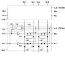
図5は、本発明の第2の実施形態に係る半導体記憶装置の構成図である。図5に示す半導体記憶装置は、メモリセルアレイ105Aとメモリセルアレイ105Bとを備える。メモリセルアレイ105Aは、メモリセル100、ワード線ドライバ回路101、メモリセル電源電圧制御回路102、OR回路OR1、ワード線WL1およびWL2、並びに、電源線VLAを備える。メモリセルアレイ105Bについては、ワード線WL3、WL4および電源線VLB以外の構成要素は、メモリセルアレイ105Aと同様であるので、図5においてはメモリセルアレイ105Bの構成の詳細は省略した。また、メモリセル100、ワード線ドライバ回路101、および、メモリセル電源電圧制御回路102は、第1の実施形態で説明したものと同じであるので、ここではこれらの構成要素の説明は省略する。
(Second Embodiment)
FIG. 5 is a configuration diagram of a semiconductor memory device according to the second embodiment of the present invention. The semiconductor memory device shown in FIG. 5 includes a
図5に示す本実施形態に係る半導体記憶装置に含まれるメモリセルアレイ105Aと、図1に示す第1の実施形態に係る半導体記憶装置とは、以下の2点で相違する。すなわち、メモリセルアレイ105Aでは、アドレス信号AD1およびAD2を入力とするOR回路OR1が、メモリセル電源電圧制御回路102の前段に設けられている。また、メモリセルアレイ105Aでは、メモリセル電源電圧制御回路102から、ワード線WL1およびWL2に接続される全てのメモリセル100に対して、同じメモリセル電源電圧VDDMAが供給される。図5に示す本実施形態に係る半導体記憶装置に含まれるメモリセルアレイ105Bと、図1に示す第1の実施形態に係る半導体記憶装置との相違点も、これと同じである。
The
以下、以上のように構成された本実施形態に係る半導体記憶装置の動作を説明する。まず、メモリセルアレイ105Aに含まれるOR回路OR1は、アドレス信号AD1とAD2の論理和を出力する。メモリセル電源電圧VDDMAは、OR回路OR1から出力された信号によって制御される。例えば、アドレス信号AD1とAD2のいずれかがHレベルであれば、OR回路OR1からは、Hレベルの信号が出力されるため、メモリセル電源電圧制御回路102から出力されるメモリセル電源電圧VDDMAは、電源電圧VDDになる。一方、アドレス信号AD1とAD2の両方がLレベルであれば、OR回路OR1からはLレベルの信号が出力されるため、メモリセル電源電圧制御回路102から出力されるメモリセル電源電圧VDDMAは、メモリ保持電圧VTPになる。
The operation of the semiconductor memory device according to this embodiment configured as described above will be described below. First, the OR circuit OR1 included in the
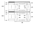
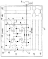
以上のような構成を有するメモリセルアレイ105A(または105B)を、実際の半導体記憶装置に配置する例を図6に示す。一般に半導体記憶装置のメモリセルアレイでは、メモリセルに含まれるP型MOSトランジスタおよびN型MOSトランジスタに基板電位を供給するために、基板電位を供給するための領域(以下、基板電位供給領域という)が一定の間隔ごとに設けられる。図6では、m行のメモリセル100ごとに基板電位供給領域103が設けられる。また、通常、基板電位供給領域103に隣接し、ワード線ドライバ回路101の占める領域であるワード線ドライバ回路領域に挟まれた部分には、回路の存在しない空白領域104が存在する。
FIG. 6 shows an example in which the
この空白領域104に、図5に示されるOR回路OR1とメモリセル電源電圧制御回路102とを配置し、さらに、基板電位供給領域103に、図5に示す電源線VLA(またはVLB)を配置することにより、半導体記憶装置の面積を増大することなく、OR回路OR1およびメモリセル電源電圧制御回路102を配置することができる。
The OR circuit OR1 and the memory cell power supply
以上のように、本実施形態に係る半導体記憶装置は、複数のワード線から供給されるアドレス信号の論理和を求めるOR回路を備え、1つのメモリセル電源電圧制御回路によって異なるワード線に接続されたメモリセルを制御する。これにより、半導体記憶装置の面積の増大を抑えつつ、第1の実施形態に係る半導体記憶装置と同様の効果を得ることができる。 As described above, the semiconductor memory device according to the present embodiment includes an OR circuit for obtaining a logical sum of address signals supplied from a plurality of word lines, and is connected to different word lines by one memory cell power supply voltage control circuit. Control the memory cell. Thereby, it is possible to obtain the same effect as that of the semiconductor memory device according to the first embodiment while suppressing an increase in the area of the semiconductor memory device.
(第3の実施形態)
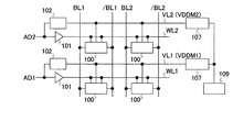
本発明の第3の実施形態に係る半導体記憶装置は、図7に示すように、第1の実施形態に係る半導体記憶装置にメモリセル電源電圧補償回路106を加えたものである。したがって、ここではメモリセル電源電圧補償回路106の構成、および、その動作について説明する。
(Third embodiment)
As shown in FIG. 7, the semiconductor memory device according to the third embodiment of the present invention is obtained by adding a memory cell power supply
メモリセル電源電圧補償回路106は、P型MOSトランジスタQP5を含んでいる。P型MOSトランジスタQP5のソース電極は、電源端子VDDに接続され、ドレイン電極は、メモリセル電源電圧VDDM1(またはVDDM2)を供給する電源線VL1(またはVL2)に接続され、ゲート電極は、接地される。メモリセル電源電圧補償回路106は、ワード線WL1(またはWL2)の状態にかかわらず、P型MOSトランジスタQP5から電源線VL1(またはVL2)に電荷を供給する。以下、図7を参照しながら、電源線VL1に接続されたメモリセル電源電圧補償回路106の動作を説明する。
Memory cell power supply
まず、Hレベルのアドレス信号AD1が入力され、ワード線WL1が活性状態になった場合を考える。この場合、メモリセル電源電圧VDDM1は電源電圧VDDと一致し、ワード線WL1に接続されるメモリセル100には電源電圧VDDが供給される。また、P型MOSトランジスタQP5のドレイン電極にも電源電圧VDDが供給される。したがって、P型MOSトランジスタQP5のソース−ドレイン間には電位差はなく、P型MOSトランジスタQP5には電流は流れない。したがって、この場合においては、メモリセル電源電圧補償回路106から電源線VL1に対して、電荷は供給されない。
First, consider a case where the address signal AD1 at H level is input and the word line WL1 is activated. In this case, the memory cell power supply voltage VDDM1 matches the power supply voltage VDD, and the power supply voltage VDD is supplied to the
次に、アドレス信号AD1がLレベルとなり、ワード線WL1が非活性状態になった場合を考える。この場合、メモリセル電源電圧VDDM1はメモリセル保持電圧VTPに一致し、ワード線WL1に接続されるメモリセル100には、メモリセル保持電圧VTPが供給される。また、P型MOSトランジスタQP5のドレイン電極にも、メモリセル保持電圧VTPが供給される。メモリセル保持電圧VTPは、電源電圧VDDよりも低いため、P型MOSトランジスタQP5のソース−ドレイン間に電位差が発生し、P型MOSトランジスタQP5に電流が流れる。すなわち、メモリセル電源電圧補償回路106は、電源線VL1に電荷を供給する。
Next, consider a case where the address signal AD1 becomes L level and the word line WL1 is inactivated. In this case, the memory cell power supply voltage VDDM1 matches the memory cell holding voltage VTP, and the memory cell holding voltage VTP is supplied to the
第1の実施形態で述べたように、メモリセル100にはリーク電流が流れる。このために、メモリセル100に供給されるメモリセル電源電圧VDDM1には電圧降下が起こる。そこで、メモリセル電源電圧補償回路106を設け、メモリセル電源電圧補償回路106から電源線VL1に供給される電荷量が、電源線VL1に接続された全てのメモリセル100におけるリーク電流による電荷の損失量と一致するようにする。これにより、非活性なワード線WL1に接続されるメモリセル100に供給されるメモリセル電源電圧VDDM1は、メモリセル保持電圧VTPに保たれる。
As described in the first embodiment, a leak current flows through the
以上のように、本実施形態に係る半導体記憶装置は、メモリセル100におけるリーク電流による電荷の損失を、メモリセル電源電圧補償回路106によって補償する。これにより、非活性なワード線に接続されるメモリセル100に対して、安定したメモリセル保持電圧を供給することができる。
As described above, in the semiconductor memory device according to this embodiment, the memory cell power supply
なお、本実施形態ではメモリセル電源電圧補償回路106を構成する要素として、P型MOSトランジスタを用いたが、リーク電流による電荷量の損失を補うことが可能な素子であれば、P型MOSトランジスタの代わりに、N型MOSトランジスタや抵抗素子などを用いてもよい。
In this embodiment, a P-type MOS transistor is used as an element constituting the memory cell power supply
また、本実施形態では、リーク電流によって損失した電荷量を、メモリセル電源電圧補償回路106によって補償する例を示したが、メモリセル電源電圧制御回路102に含まれるP型MOSトランジスタQP3も同様に、メモリセル100に対して、電荷を供給する構成を有する。したがって、メモリセル電源電圧補償回路106を設計する場合には、P型MOSトランジスタQP3の電荷供給能力を考慮して設計してもよい。これにより、メモリセル電源電圧補償回路106によって補償する電荷量を低減することも可能である。特に、メモリセルにおけるリーク電流による電荷の損失量を補償できるだけの十分な電荷供給能力がP型MOSトランジスタQP3にある場合には、メモリセル電源電圧補償回路106を設けなくとも良い。これにより、メモリセル電源電圧補償回路106を除去することができ、回路の面積を小さくできる。
Further, in this embodiment, the example in which the amount of charge lost due to the leakage current is compensated by the memory cell power supply
(第4の実施形態)
本発明の第4の実施形態に係る半導体記憶装置は、図8に示すように、第1の実施形態に係る半導体記憶装置にメモリセル電源電圧補償回路107、および、メモリセル保持参照電圧発生回路109を加えたものである。したがって、ここでは、メモリセル電源電圧補償回路107およびメモリセル保持参照電圧発生回路109について、回路の構成およびその動作を説明する。
(Fourth embodiment)
As shown in FIG. 8, the semiconductor memory device according to the fourth embodiment of the present invention includes a memory cell power supply
図8に示すように、メモリセル電源電圧補償回路107の一端は、電源線VL1(またはVL2)に接続され、他端はメモリセル保持参照電圧発生回路109の出力に接続される。
As shown in FIG. 8, one end of the memory cell power supply
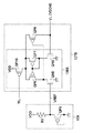
図9に、メモリセル電源電圧補償回路107の構成の一例(以下、メモリセル電源電圧補償回路107Aという)と、メモリセル保持参照電圧発生回路109の構成とを示す。図9に示すメモリセル電源電圧補償回路107Aは、P型MOSトランジスタQP6〜QP8、並びに、N型MOSトランジスタQN5およびQN6を備える。
FIG. 9 shows an example of the configuration of the memory cell power supply voltage compensation circuit 107 (hereinafter referred to as the memory cell power supply
P型MOSトランジスタQP6およびQP7のソース電極は、共に電源端子VDDに接続され、ドレイン電極は、それぞれN型MOSトランジスタQN5およびQN6のドレイン電極に接続される。また、P型MOSトランジスタQP6およびQP7のゲート電極は、共にP型MOSトランジスタQP7のドレイン電極に接続される。一方、N型MOSトランジスタQN5およびQN6のソース電極は共に接地され、ゲート電極は、それぞれ、メモリセル保持参照電圧発生回路109の出力および電源線VLに接続される。
The source electrodes of P-type MOS transistors QP6 and QP7 are both connected to power supply terminal VDD, and the drain electrodes are connected to the drain electrodes of N-type MOS transistors QN5 and QN6, respectively. The gate electrodes of P-type MOS transistors QP6 and QP7 are both connected to the drain electrode of P-type MOS transistor QP7. On the other hand, the source electrodes of N-type MOS transistors QN5 and QN6 are both grounded, and the gate electrodes are connected to the output of memory cell holding reference
P型MOSトランジスタQP6およびQP7、並びに、N型MOSトランジスタQN5およびQN6は、差動増幅回路108Aを構成する。差動増幅回路108Aの出力は、P型MOSトランジスタQP8のゲート電極に接続される。また、P型MOSトランジスタQP8のソース電極は、電源端子VDDに接続され、ドレイン電極は、電源線VLに接続される。
P-type MOS transistors QP6 and QP7 and N-type MOS transistors QN5 and QN6 constitute a
メモリセル電源電圧補償回路107Aには、メモリセル保持参照電圧発生回路109が接続される。メモリセル保持参照電圧発生回路109は、ダイオード型にゲート接続されたP型MOSトランジスタQP9と、抵抗素子R1とを備える。メモリセル保持参照電圧発生回路109の出力(P型MOSトランジスタQP9と抵抗R1の接合部)からは、メモリ保持参照電圧VREFが出力される。このP型MOSトランジスタQP9は、メモリセルに含まれるP型MOSトランジスタと同じ特性を有することから、メモリセル保持参照電圧発生回路109から出力されるメモリ保持参照電圧VREFは、メモリ保持電圧VTPと一致する。
A memory cell holding reference
以下、図9を参照しながらメモリセル電源電圧補償回路107Aの動作を説明する。メモリセル電源電圧補償回路107Aにメモリセル電源電圧VDDMが供給されると、差動増幅回路108Aは、メモリセル電源電圧VDDMとメモリセル保持参照電圧VREFとを比較し、その結果を増幅してP型MOSトランジスタQP8のゲート電極に出力する。メモリセル電源電圧VDDMがメモリセル保持参照電圧VREFよりも低い場合には、差動増幅回路108Aは、Lレベルの信号をP型MOSトランジスタQP8のゲート電極に出力する。また、メモリセル電源電圧VDDMが、メモリセル保持参照電圧VREFよりも高い場合には、差動増幅回路108Aは、Hレベルの信号をP型MOSトランジスタQP8のゲート電極に出力する。
Hereinafter, the operation of the memory cell power supply
P型MOSトランジスタQP8のゲート電極に差動増幅回路108AからLレベルの信号が入力されると、P型MOSトランジスタQP8はオンになり、電源端子VDDから電源線VLに対して電荷が供給される。したがって、メモリセル電源電圧VDDMは上昇する。一方、P型MOSトランジスタQP8のゲート電極に差動増幅回路108AからHレベルの信号が入力されると、P型MOSトランジスタQP8はオフになり、メモリセル電源電圧VDDMには影響はない。
When an L level signal is input from the
メモリセル電源電圧VDDMがメモリセル保持参照電圧VREFよりも低い場合には、メモリセル電源電圧VDDMは、差動増幅回路108Aにより、メモリセル保持参照電圧VREFに一致するまで上昇する。メモリセル電源電圧VDDMがメモリセル保持参照電圧VREFに一致するまで上昇すると、P型MOSトランジスタQP8はオフになり、メモリセル電源電圧VDDMの上昇が止まる。このようにして、メモリセル電源電圧補償回路107Aは、メモリセル電源電圧VDDMの電圧が降下した場合において、差動増幅回路108AとP型MOSトランジスタQP8との作用により、メモリセル電源電圧VDDMの電圧を上げる。特に、メモリセル電源電圧VDDMがメモリセル保持電圧VTPである場合には、メモリセル電源電圧補償回路107Aは、メモリセル電源電圧をメモリセル保持参照電圧VREF付近に保持する。
When the memory cell power supply voltage VDDM is lower than the memory cell holding reference voltage VREF, the memory cell power supply voltage VDDM is increased by the
第3の実施形態ですでに述べたように、非活性なワード線に接続されるメモリセルに供給されるメモリセル電源電圧VDDMは、リーク電流の影響により、メモリセル保持電圧VTPから降下する場合がある。しかし、本実施形態に係る半導体記憶装置は、メモリセル電源電圧補償回路107Aを備えることにより、非活性なメモリセルからのリーク電流によるメモリセル電源電圧VDDMの電圧降下を補償する。これにより、メモリセルに安定したメモリセル電源電圧VDDMを供給することができる。
As already described in the third embodiment, the memory cell power supply voltage VDDM supplied to the memory cells connected to the inactive word line drops from the memory cell holding voltage VTP due to the influence of the leakage current. There is. However, the semiconductor memory device according to the present embodiment includes the memory cell power supply
次に、図10にメモリセル電源電圧補償回路107の他の構成例(以下、メモリセル電源電圧補償回路107Bという)を示す。図10に示すメモリセル電源電圧補償回路107Bは、ワード線WLで制御されるP型MOSトランジスタQP10を、メモリセル電源電圧補償回路107Aに追加したものである。P型MOSトランジスタQP10のソース電極は、電源端子VDDに接続され、ドレイン電極は、P型MOSトランジスタQP6〜QP8に接続され、ゲート電極は、ワード線WLに接続される。その他の構成要素については、メモリセル電源電圧補償回路107Aと同じである。
Next, FIG. 10 shows another configuration example of the memory cell power supply voltage compensation circuit 107 (hereinafter referred to as the memory cell power supply
以上のように構成されたメモリセル電源電圧補償回路107Bの動作を説明する。まず、ワード線WLからP型MOSトランジスタQP10にLレベルの信号が入力された場合には、P型MOSトランジスタQP10はオンになり、メモリセル電源電圧補償回路107Bは、メモリセル電源電圧補償回路107Aと同様の動作を行う。
The operation of the memory cell power supply
次に、ワード線WLからP型MOSトランジスタQP10にHレベルの信号が入力された場合には、P型MOSトランジスタQP10はオフになり、差動増幅回路108BおよびP型MOSトランジスタQP8は動作しない。したがって、メモリセル電源電圧補償回路107Bは、メモリセルが非活性な場合にのみ動作を行う。
Next, when an H level signal is input from the word line WL to the P-type MOS transistor QP10, the P-type MOS transistor QP10 is turned off and the
以上のように、図10に示すメモリセル電源電圧補償回路107Bを備えた半導体記憶装置は、P型MOSトランジスタQP10によって差動増幅回路108Bの動作を制御することにより、メモリセル電源電圧補償回路107Bが必要なメモリセルが非活性な場合においてのみ、差動増幅回路108Bを動作させる。これにより、メモリセル電源電圧補償回路107Bにおいて消費される電力を最小限に抑えることができる。
As described above, the semiconductor memory device including the memory cell power supply
(第5の実施形態)
図11は、本発明の第5の実施形態に係る半導体記憶装置の構成図である。図11に示す半導体記憶装置は、メモリセル100、ワード線ドライバ回路101、メモリセル電源電圧制御回路202、ビット線プリチャージ回路300、ビット線プリチャージ制御回路301、ワード線WL1およびWL2、ビット線BL1、BL2、/BL1および/BL2、電源線VL1およびVL2、ビット線プリチャージ制御信号線/IPCG、並びに、メモリセル電荷供給線VSを備える。メモリセル100およびワード線ドライバ回路101は、第1の実施形態で説明したものと同じであるので、ここではこれらの構成要素の説明は省略する。
(Fifth embodiment)
FIG. 11 is a configuration diagram of a semiconductor memory device according to the fifth embodiment of the present invention. 11 includes a
ビット線プリチャージ回路300は、ビット線BL1および/BL1(またはBL2および/BL2)、並びに、ビット線プリチャージ制御信号線/IPCGに接続される。また、ビット線プリチャージ制御回路301は、ビット線プリチャージ制御信号線/IPCG、および、メモリセル電荷供給線VSに接続される。ビット線プリチャージ制御回路301には、外部からビット線プリチャージ信号/PCGが入力される。本実施形態に係る半導体記憶装置は、ビット線プリチャージ回路300、および、ビット線プリチャージ制御回路301を備えることにより、ビット線BL1、BL2、/BL1および/BL2を、Hレベルまたはハイインピーダンス状態に制御する。
Bit line
次に、図12を参照しながらメモリセル電源電圧制御回路202の構成を説明する。メモリセル電源電圧制御回路202と、図3に示すメモリセル電源電圧制御回路102とは以下の点で相違する。すなわち、メモリセル電源電圧制御回路202に含まれるN型MOSトランジスタQN5のソース電極は、メモリセル電荷供給線VSを介して、ビット線プリチャージ制御回路301に接続される。その他の構成要素については、メモリセル電源電圧制御回路102と同じであるので、ここでは説明を省略する。また、メモリセル電源電圧制御回路202は、メモリセル電源電圧制御回路102と同様に、メモリセルが接続されるワード線の状態(活性あるいは非活性)に応じて、メモリセルに供給する電源電圧を制御する。
Next, the configuration of the memory cell power supply
次に、図13を参照しながらビット線プリチャージ回路300の構成を説明する。ビット線プリチャージ回路300は、P型MOSトランジスタQP11〜QP13、および、インバータINV6を備える。インバータINV6の入力は、ビット線プリチャージ制御信号線/IPCGに接続される。また、インバータINV6の出力は、P型MOSトランジスタQP11〜QP13のゲート電極に接続される。
Next, the configuration of the bit line
P型MOSトランジスタQP11およびQP12のソース電極は、いずれも電源端子VDDに接続される。また、P型MOSトランジスタQP11およびQP12のドレイン電極は、それぞれ、ビット線BLおよび/BLに接続される。P型MOSトランジスタQP13のソース電極およびドレイン電極は、それぞれ、ビット線BLおよび/BLに接続される。 The source electrodes of P-type MOS transistors QP11 and QP12 are both connected to power supply terminal VDD. The drain electrodes of P-type MOS transistors QP11 and QP12 are connected to bit lines BL and / BL, respectively. The source electrode and drain electrode of P-type MOS transistor QP13 are connected to bit lines BL and / BL, respectively.
以上のように構成されたビット線プリチャージ回路300の動作を説明する。ビット線プリチャージ制御信号線/IPCGからHレベルの信号がインバータINV6に入力されると、P型MOSトランジスタQP11〜QP13のゲート電極は、Lレベルとなる。この結果、P型MOSトランジスタQP11〜QP13がオンになるため、ビット線BLおよび/BLは、Hレベルにプリチャージされる。
The operation of the bit line
一方、ビット線プリチャージ制御信号線/IPCGからLレベルの信号がインバータINV6に入力されると、P型MOSトランジスタQP11〜QP13のゲート電極は、Hレベルとなる。この結果、P型MOSトランジスタQP11〜QP13がオフになるため、ビット線BLおよび/BLは、ハイインピーダンス状態になる。 On the other hand, when an L level signal is input to inverter INV6 from bit line precharge control signal line / IPCG, the gate electrodes of P-type MOS transistors QP11 to QP13 are at the H level. As a result, P-type MOS transistors QP11-QP13 are turned off, so that bit lines BL and / BL are in a high impedance state.
一般に半導体記憶装置に設けられる各ビット線プリチャージ回路は、全てのワード線が非活性状態である場合には活性状態に制御され、各ビット線をHレベルにプリチャージする。一方、いずれかのワード線が活性状態である場合には、各ビット線プリチャージ回路は非活性状態に制御され、各ビット線に影響を与えない。したがって、この場合、各ビット線はハイインピーダンス状態になる。以下、ビット線プリチャージ回路300が、ビット線プリチャージ制御回路301によって制御されることにより、同様の動作をすることを説明する。
In general, each bit line precharge circuit provided in a semiconductor memory device is controlled to be active when all word lines are inactive, and precharges each bit line to H level. On the other hand, when any one of the word lines is in an active state, each bit line precharge circuit is controlled to be in an inactive state and does not affect each bit line. Therefore, in this case, each bit line is in a high impedance state. Hereinafter, it will be described that the bit line
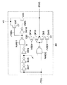
まず、図14を参照しながらビット線プリチャージ制御回路301の構成を説明する。ビット線プリチャージ制御回路301は、N型MOSトランジスタQN7〜QN10、P型MOSトランジスタQP14およびQP15、インバータINV7〜INV10、並びに、NAND回路NAND1およびNAND2を備える。
First, the configuration of the bit line
N型MOSトランジスタQN7のドレイン電極は、メモリセル電荷供給線VSに接続され、ソース電極は接地される。また、N型MOSトランジスタQN7のゲート電極は、NAND回路NAND1の出力に接続される。以下、N型MOSトランジスタQN7のゲート電極とNAND回路NAND1の出力とを接続するノードをノード/VSENと呼ぶ。N型MOSトランジスタQN7は、NAND回路NAND1から出力される信号に応じて、メモリセル電荷供給線VSと接地とを導通または開放する。 The drain electrode of N-type MOS transistor QN7 is connected to memory cell charge supply line VS, and the source electrode is grounded. The gate electrode of N-type MOS transistor QN7 is connected to the output of NAND circuit NAND1. Hereinafter, a node connecting the gate electrode of N-type MOS transistor QN7 and the output of NAND circuit NAND1 is referred to as node / VSEN. N-type MOS transistor QN7 conducts or opens memory cell charge supply line VS and ground in accordance with a signal output from NAND circuit NAND1.
N型MOSトランジスタQN8のドレイン電極は、メモリセル電荷供給線VSに接続され、ソース電極は、ビット線プリチャージ制御信号線/IPCGに接続される。また、N型MOSトランジスタQN8のゲート電極は、インバータINV10の出力に接続される。以下、N型トランジスタQN8のゲート電極とインバータINV10の出力とを接続するノードをノードVSENと呼ぶ。N型MOSトランジスタQN8は、インバータINV10から出力される信号に応じて、メモリセル電荷供給線VSとビット線プリチャージ制御信号線/IPCGとを導通または開放する。 N-type MOS transistor QN8 has a drain electrode connected to memory cell charge supply line VS and a source electrode connected to bit line precharge control signal line / IPCG. The gate electrode of N-type MOS transistor QN8 is connected to the output of inverter INV10. Hereinafter, a node connecting the gate electrode of N-type transistor QN8 and the output of inverter INV10 is referred to as node VSEN. N-type MOS transistor QN8 conducts or opens memory cell charge supply line VS and bit line precharge control signal line / IPCG in accordance with a signal output from inverter INV10.
N型MOSトランジスタQN9およびQN10、並びに、P型MOSトランジスタQP14およびQP15は、クロックインバータを構成する。以下に、その構成を説明する。 N-type MOS transistors QN9 and QN10 and P-type MOS transistors QP14 and QP15 constitute a clock inverter. The configuration will be described below.
N型MOSトランジスタQN9のソース電極は、N型MOSトランジスタQN10のドレイン電極に接続され、ドレイン電極は、ビット線プリチャージ制御信号線/IPCGに接続される。また、N型MOSトランジスタQN9のゲート電極は、NAND回路NAND2の出力に接続される。N型MOSトランジスタQN10のソース電極は接地され、ゲート電極は、ノード/VSENを介して、NAND回路NAND1の出力に接続される。 The source electrode of N-type MOS transistor QN9 is connected to the drain electrode of N-type MOS transistor QN10, and the drain electrode is connected to bit line precharge control signal line / IPCG. The gate electrode of N-type MOS transistor QN9 is connected to the output of NAND circuit NAND2. The source electrode of N-type MOS transistor QN10 is grounded, and the gate electrode is connected to the output of NAND circuit NAND1 via node / VSEN.
P型MOSトランジスタQP14のソース電極は、電源端子VDDに接続され、ドレイン電極は、P型MOSトランジスタQP15のソース電極に接続される。また、P型MOSトランジスタQP14のゲート電極は、ノードVSENを介して、インバータINV10の出力に接続される。P型MOSトランジスタQP15のドレイン電極は、ビット線プリチャージ制御信号線/IPCGに接続され、ゲート電極は、NAND回路NAND2の出力に接続される。 The source electrode of the P-type MOS transistor QP14 is connected to the power supply terminal VDD, and the drain electrode is connected to the source electrode of the P-type MOS transistor QP15. The gate electrode of the P-type MOS transistor QP14 is connected to the output of the inverter INV10 via the node VSEN. The drain electrode of P-type MOS transistor QP15 is connected to bit line precharge control signal line / IPCG, and the gate electrode is connected to the output of NAND circuit NAND2.
以上のように構成されるクロックインバータは、NAND回路NAND2から出力される信号、NAND回路NAND1から出力される信号、および、インバータINV10から出力される信号に応じて、ビット線プリチャージ制御信号線/IPCGをHレベル、Lレベルあるいはハイインピーダンス状態に制御する。 The clock inverter configured as described above has the bit line precharge control signal line / in response to the signal output from the NAND circuit NAND2, the signal output from the NAND circuit NAND1, and the signal output from the inverter INV10. Control IPCG to H level, L level or high impedance state.
次に、インバータINV7〜INV9、並びに、NAND回路NAND1およびNAND2について説明する。インバータINV7〜INV9は、直列に接続される。インバータINV7には、ビット線プリチャージ信号/PCGが入力される。インバータINV9の出力には、NAND回路NAND1の一方の入力が接続される。以下、インバータINV9とNAND回路NAND1とを接続するノードをノードBと呼ぶ。インバータINV7〜INV9は、このノードBを介してNAND回路NAND1に入力される信号を遅延する。また、NAND回路NAND1の他方の入力には、ビット線プリチャージ信号/PCGが入力される。 Next, inverters INV7 to INV9 and NAND circuits NAND1 and NAND2 will be described. Inverters INV7 to INV9 are connected in series. Bit line precharge signal / PCG is input to inverter INV7. One input of the NAND circuit NAND1 is connected to the output of the inverter INV9. Hereinafter, a node connecting the inverter INV9 and the NAND circuit NAND1 is referred to as a node B. Inverters INV7 to INV9 delay a signal input to NAND circuit NAND1 via node B. A bit line precharge signal / PCG is input to the other input of the NAND circuit NAND1.
また、NAND回路NAND2の一方の入力には、ビット線プリチャージ信号/PCGが入力される。NAND回路NAND2の他方の入力は、インバータINV8の出力に接続される。以下、NAND回路NAND2とインバータINV8とを接続するノードをノードAと呼ぶ。 A bit line precharge signal / PCG is input to one input of the NAND circuit NAND2. The other input of the NAND circuit NAND2 is connected to the output of the inverter INV8. Hereinafter, a node connecting the NAND circuit NAND2 and the inverter INV8 is referred to as a node A.
次に、以上のように構成されたビット線プリチャージ制御回路301の動作を説明する。Hレベルのビット線プリチャージ信号/PCGがビット線プリチャージ制御回路301に入力された場合、NAND回路NAND1には、Hレベルのビット線プリチャージ信号/PCG、および、ノードBを介してLレベルの信号が入力される。したがって、NAND回路NAND1は、Hレベルの信号をN型MOSトランジスタQN7のゲート電極、および、インバータINV10に出力する。この結果、N型MOSトランジスタQN7がオンになることから、図12に示すN型MOSトランジスタQN5のソース電極は、メモリセル電荷供給線VSを介して接地される。また、インバータINV10は、N型MOSトランジスタQN8のゲート電極に、Lレベルの信号を出力することから、N型MOSトランジスタQN8はオフになる。
Next, the operation of the bit line
また、NAND回路NAND2には、Hレベルのビット線プリチャージ信号/PCG、および、ノードAを介してHレベルの信号が入力される。したがって、NAND回路NAND2は、Lレベルの信号をクロックインバータに出力する。ノードVSENにはインバータINV10からLレベルの信号が出力されるため、P型MOSトランジスタQP14はオンになる。また、P型MOSトランジスタQP15には、NAND回路NAND2からLレベルの信号が出力されるため、P型MOSトランジスタQP15はオンになる。したがって、ビット線プリチャージ制御信号線/IPCGには、クロックインバータからHレベルの信号が供給される。 The NAND circuit NAND2 receives an H level bit line precharge signal / PCG and an H level signal via the node A. Therefore, the NAND circuit NAND2 outputs an L level signal to the clock inverter. Since the L level signal is output from the inverter INV10 to the node VSEN, the P-type MOS transistor QP14 is turned on. Further, since the L-level signal is output from the NAND circuit NAND2 to the P-type MOS transistor QP15, the P-type MOS transistor QP15 is turned on. Therefore, an H level signal is supplied from the clock inverter to bit line precharge control signal line / IPCG.
一方、Lレベルのビット線プリチャージ信号/PCGが、ビット線プリチャージ制御回路301に入力された場合には、NAND回路NAND1およびNAND2から、共にHレベルの信号が出力される。この結果、N型MOSトランジスタQN9およびQN10は共にオンになり、ビット線プリチャージ制御信号線/IPCGは接地される。また、この場合も、N型MOSトランジスタQN7がオンになることから、N型MOSトランジスタQN5のソース電極は、メモリセル電荷供給線VSを介して接地される。
On the other hand, when the bit line precharge signal / PCG at the L level is input to the bit line
以上のように、ビット線プリチャージ制御回路301は、ビット線プリチャージ信号/PCGがHレベルの場合には、ビット線プリチャージ制御信号線/IPCGに供給する信号をHレベルに制御し、また、ビット線プリチャージ信号/PCGがLレベルの場合には、ビット線プリチャージ制御信号線/IPCGに供給する信号をLレベルに制御する。
As described above, bit line
また、上述したように、ビット線プリチャージ制御信号線/IPCGにHレベルの信号が供給されると、ビット線プリチャージ回路300は、ビット線BLおよび/BLをプリチャージする。また、ビット線プリチャージ制御信号線/IPCGにLレベルの信号が供給されると、ビット線プリチャージ回路300は、ビット線BLおよび/BLに影響を与えない。したがって、ビット線BLおよび/BLは、ハイインピーダンス状態になる。
As described above, when an H level signal is supplied to the bit line precharge control signal line / IPCG, the bit line
さらに、本実施形態に係る半導体記憶装置は、全てのワード線が非活性状態である場合には、Hレベルのビット線プリチャージ信号/PCGがビット線プリチャージ制御回路301に入力されることにより、ビット線プリチャージ制御信号線/IPCGに接続された全てのビット線プリチャージ回路300を活性状態に制御し、全てのビット線BL1、BL2、/BL1および/BL2をプリチャージする。
Further, in the semiconductor memory device according to the present embodiment, when all the word lines are inactive, an H level bit line precharge signal / PCG is input to the bit line
また、いずれかのワード線が活性状態である場合には、Lレベルのビット線プリチャージ信号/PCGが、ビット線プリチャージ制御回路301に入力されることにより、本実施形態に係る半導体記憶装置は、ビット線プリチャージ制御信号線/IPCGに接続された全てのビット線プリチャージ回路300を非活性状態に制御し、全てのビット線BL1、BL2、/BL1および/BL2をハイインピーダンス状態にする。
When any one of the word lines is in an active state, the L-level bit line precharge signal / PCG is input to the bit line
以上のように、本実施形態に係る半導体記憶装置は、ビット線プリチャージ制御回路301を備えることにより、ビット線プリチャージ回路300を一般のビット線プリチャージ回路と同様に動作させる。
As described above, the semiconductor memory device according to the present embodiment includes the bit line
また、ビット線プリチャージ制御回路301に入力されるビット線プリチャージ信号/PCGが、HレベルまたはLレベルいずれの場合にも、図12に示すN型MOSトランジスタQN5のソース電極は、メモリセル電荷供給線VSを介して接地されることから、メモリセル電源電圧制御回路202は、第1の実施形態におけるメモリセル電源電圧制御回路102と同様に動作する。したがって、本実施形態に係る半導体記憶装置は、第1の実施形態に係る半導体記憶装置と同様に、半導体記憶装置の低消費電力化や高速化といった効果を有する。
Further, regardless of whether the bit line precharge signal / PCG input to the bit line
さらに、本実施形態に係る半導体記憶装置は、上記の効果に加えて、電源線VL1(またはVL2)に蓄積された電荷を、ビット線プリチャージ制御信号線/IPCGに供給することによって電荷を再利用することにより、半導体記憶装置のさらなる低消費電力化を実現する。以下、この効果を図14を参照しながら詳しく説明する。 Furthermore, in addition to the above effect, the semiconductor memory device according to the present embodiment recharges the charge by supplying the charge accumulated in the power supply line VL1 (or VL2) to the bit line precharge control signal line / IPCG. By using it, further reduction in power consumption of the semiconductor memory device is realized. Hereinafter, this effect will be described in detail with reference to FIG.
例えば、図11において、アドレス信号AD1がHレベルからLレベルへと変わり、ワード線WL1が活性状態から非活性状態に変わる場合を考える。ワード線WL1が非活性状態になると、ワード線WL1に接続された全てのメモリセル100が非活性状態になる。この場合、第1の実施形態に係る半導体記憶装置においては、図1に示すメモリセル電源電圧制御回路102によって、メモリセル電源電圧VDDM1が電源電圧VDDからVTPに変わる際、電源線VL1に蓄えられていた電荷は、N型MOSトランジスタQN5のソース電極から接地端子に排出される。
For example, consider the case where the address signal AD1 changes from H level to L level in FIG. 11 and the word line WL1 changes from the active state to the inactive state. When the word line WL1 is deactivated, all the
これに対して、本実施形態に係る半導体記憶装置では、ワード線WL1が非活性状態になり、さらに、ビット線プリチャージ信号/PCGがLレベルからHレベルに変わると、ビット線プリチャージ制御回路301に設けられたインバータINV7〜INV9による遅延時間の間、NAND回路NAND1の2つの入力が共にHレベルとなる。したがって、この時間の間ではNAND回路NAND1からLレベルの信号が出力され、この結果、N型MOSトランジスタQN7がオフになり、N型MOSトランジスタQN8がオンになる。 In contrast, in the semiconductor memory device according to the present embodiment, when the word line WL1 is deactivated and the bit line precharge signal / PCG changes from the L level to the H level, the bit line precharge control circuit During the delay time by the inverters INV7 to INV9 provided in 301, both two inputs of the NAND circuit NAND1 become H level. Therefore, during this time, an L level signal is output from the NAND circuit NAND1, and as a result, the N-type MOS transistor QN7 is turned off and the N-type MOS transistor QN8 is turned on.
N型MOSトランジスタQN7がオフ状態であり、N型MOSトランジスタQN8がオン状態であると、メモリセル電源電圧制御回路202に含まれるN型MOSトランジスタQN5と、ビット線プリチャージ制御信号線/IPCGとが導通する。この結果、メモリセル電源電圧VDDM1が電源電圧VDDからVTPに変わる際、電源VL1に蓄えられていた電荷は、メモリセル電荷供給線VSを介して、ビット線プリチャージ制御信号線/IPCGに供給される。
When N-type MOS transistor QN7 is off and N-type MOS transistor QN8 is on, N-type MOS transistor QN5 included in memory cell power supply
また、このときノードVSENはHレベルであり、ノード/VSENはLレベルであるため、クロックインバータの出力はハイインピーダンス状態であり、クロックインバータは、ビット線プリチャージ制御信号線/IPCGに影響を与えない。 At this time, since the node VSEN is at the H level and the node / VSEN is at the L level, the output of the clock inverter is in a high impedance state, and the clock inverter affects the bit line precharge control signal line / IPCG. Absent.
以上の動作をタイミングチャートに示したものが図15である。図15は、ワード線WLがHレベルからLレベルに変わり、ビット線プリチャージ信号/PCGがLレベルからHレベルに変わる場合に、ビット線プリチャージ信号/PCGが入力されてから、ノードBに供給される信号がLレベルに変わるまでの時間tの間(すなわち、インバータINV7〜INV9による遅延時間の間)、ビット線プリチャージ制御信号線/IPCGに電源線VL1から電荷が供給され、供給された電荷によってビット線プリチャージ制御信号線/IPCGの電位が徐々に上昇することを示す。 FIG. 15 shows the above operation in a timing chart. FIG. 15 shows that when the word line WL changes from H level to L level and the bit line precharge signal / PCG changes from L level to H level, the bit line precharge signal / PCG is input to the node B after the bit line precharge signal / PCG is input. Charge is supplied from the power supply line VL1 to the bit line precharge control signal line / IPCG for the time t until the supplied signal changes to L level (that is, during the delay time by the inverters INV7 to INV9). This shows that the potential of the bit line precharge control signal line / IPCG gradually increases due to the accumulated charges.
以上のように、本実施形態に係る半導体記憶装置は、ワード線が活性状態から非活性状態に変わる場合において、電源線VLに蓄えられた電荷をビット線プリチャージ制御信号線/IPCGに供給し電荷を再利用する。これにより、半導体記憶装置のさらなる低消費電力化が実現される。 As described above, the semiconductor memory device according to the present embodiment supplies the charge stored in the power supply line VL to the bit line precharge control signal line / IPCG when the word line changes from the active state to the inactive state. Reuse charge. Thereby, further reduction in power consumption of the semiconductor memory device is realized.
(第6の実施形態)
図16は、本発明の第6の実施形態に係る半導体記憶装置の構成図である。図16に示す半導体記憶装置は、メモリセルアレイ110およびメモリセルアレイ111を含む。メモリセルアレイ110は、メモリセル100、ワード線ドライバ回路101、メモリセル電源電圧制御回路102、ワード線WL1およびWL2、電源線VL1およびVL2、N型MOSトランジスタQN11、AND回路AND1、並びに、インバータINV11を備える。メモリセルアレイ111に含まれるワード線WLRおよび電源線VLR以外の構成要素は、メモリセルアレイ110と同様である。また、メモリセル100、ワード線ドライバ回路101、および、メモリセル電源電圧制御回路102は、第1の実施形態で説明したものと同じであるので、ここではこれらの構成要素の説明は省略する。
(Sixth embodiment)
FIG. 16 is a configuration diagram of a semiconductor memory device according to the sixth embodiment of the present invention. The semiconductor memory device shown in FIG. 16 includes a
一般に半導体記憶装置は、製品の歩留まりの向上のために、正規のメモリセルアレイ以外に、予め予備のメモリセルアレイを搭載している。半導体記憶装置の検査工程において、正規のメモリセルアレイ内に欠陥のあるメモリセルが存在すると判定された場合には、その欠陥箇所を予備のメモリセルによって置換し、その半導体記憶装置を良品として完成させる、いわゆる冗長救済が行われる。本実施形態に係る半導体記憶装置は、メモリセルアレイ111を、正規のメモリセルアレイ110のための冗長救済用のメモリセルアレイ(以下、冗長救済ブロックという)として備える。
In general, a semiconductor memory device has a spare memory cell array mounted in advance in addition to a regular memory cell array in order to improve product yield. In the inspection process of the semiconductor memory device, when it is determined that a defective memory cell exists in the regular memory cell array, the defective portion is replaced with a spare memory cell, and the semiconductor memory device is completed as a non-defective product. So-called redundant relief is performed. The semiconductor memory device according to the present embodiment includes the
以下、上記の冗長救済ブロックの構成について説明する。冗長救済ブロックには、外部からアドレス信号ADRと冗長救済アドレス信号RADRとが入力される。冗長救済アドレス信号RADRは分岐され、一方はAND回路AND1に、他方はインバータINV11に入力される。冗長救済ブロックは、これらアドレス信号ADRおよび冗長救済アドレス信号RADRによって制御される。以下、図16を参照しながら冗長救済ブロックの動作を説明する。 Hereinafter, the configuration of the redundant relief block will be described. The redundancy relief block receives an address signal ADR and a redundancy relief address signal RADR from the outside. The redundant relief address signal RADR is branched and one is input to the AND circuit AND1 and the other is input to the inverter INV11. The redundant relief block is controlled by these address signal ADR and redundant relief address signal RADR. Hereinafter, the operation of the redundant relief block will be described with reference to FIG.
まず、冗長救済が行われない場合について説明する。冗長救済が行われない場合には、冗長救済ブロックに入力されるアドレス信号ADR、および、冗長救済アドレス信号RADRは、共にLレベルに設定される。したがって、AND回路AND1の各入力信号はLレベルであるため、AND回路AND1からは、Lレベルの信号が出力される。出力されたLレベルの信号はワード線WLRに入力されるため、冗長救済ブロックに含まれるメモリセル100は非活性状態になる。したがって、ワード線WLRに接続されるメモリセル100は、ビット線BL1、BL2、/BL1および/BL2には影響を与えない。
First, a case where redundant relief is not performed will be described. When redundant relief is not performed, both the address signal ADR and the redundant relief address signal RADR input to the redundant relief block are set to the L level. Accordingly, since each input signal of the AND circuit AND1 is at L level, an L level signal is output from the AND circuit AND1. Since the output L level signal is input to the word line WLR, the
また、分岐された冗長救済アドレス信号RADRの他方は、インバータINV11によってHレベルに変換され、変換された信号は、N型MOSトランジスタQN11のゲート電極に入力される。N型MOSトランジスタQN11は、ゲート電極にHレベルの信号が入力されたためにオンになる。これにより、電源線VLRは接地され、メモリセル電源電圧VDDMRは接地レベルになる。 The other of the branched redundant relief address signal RADR is converted to H level by inverter INV11, and the converted signal is input to the gate electrode of N-type MOS transistor QN11. The N-type MOS transistor QN11 is turned on because an H level signal is input to the gate electrode. As a result, power supply line VLR is grounded, and memory cell power supply voltage VDDMR is at the ground level.
冗長救済が行われない場合には、正規のメモリセルアレイに入力される冗長救済アドレス信号RAD1は、Hレベルに設定される。したがって、正規のメモリセルアレイに含まれるAND回路AND1からは、アドレス信号AD1と同じ信号が出力される。AND回路AND1から出力された信号は、ワード線ドライバ回路101およびメモリセル電源電圧制御回路102に入力される。
When the redundancy relief is not performed, the redundancy relief address signal RAD1 input to the normal memory cell array is set to the H level. Therefore, the same signal as the address signal AD1 is output from the AND circuit AND1 included in the normal memory cell array. The signal output from the AND circuit AND1 is input to the word
また、正規メモリセルに含まれるN型MOSトランジスタQN11のゲート電極には、インバータINV11によってLレベルに変換された冗長救済アドレス信号RAD1が入力される。このため、N型MOSトランジスタはオフになり、電源線VL1には、メモリセル電源電圧制御回路102から出力されるメモリセル電源電圧VDDM1が供給される。
The redundant relief address signal RAD1 converted to the L level by the inverter INV11 is input to the gate electrode of the N-type MOS transistor QN11 included in the normal memory cell. Therefore, the N-type MOS transistor is turned off, and the memory cell power supply voltage VDDM1 output from the memory cell power supply
以上のように、冗長救済が行われない場合には、冗長救済ブロックは、正規のメモリセルアレイ110に影響を与えず、正規のメモリセルアレイは、通常の動作を行う。また、本実施形態の半導体記憶装置は、冗長救済ブロックに含まれる非活性なメモリセル100のメモリセル電源電圧VDDMRを、N型MOSトランジスタQN11によって接地レベルにすることにより、これらメモリセル100からのリーク電流を削減し、半導体記憶装置の消費電力を抑える。
As described above, when redundant relief is not performed, the redundant relief block does not affect the normal
次に、冗長救済が行われる場合について説明する。ここでは、例えば、ワード線WL1に接続されるメモリセル100のいずれかに欠陥があるとし、ワード線WL1に接続されるメモリセル100が冗長救済により、冗長救済ブロック内のワード線WLRに接続されるメモリセル100に置換されるとする。すなわち、メモリセルアレイ111によってメモリセルアレイ112が置換される場合を考える。
Next, a case where redundant relief is performed will be described. Here, for example, it is assumed that one of the
この場合、冗長救済信号RAD1はLレベルに、冗長救済信号RAD2およびRADRはHレベルに設定される。また、アドレス信号AD1が選択される代わりに、冗長救済用のアドレス信号ADRが選択されるように設定される。アドレス信号AD1はLレベルに設定される。 In this case, redundant relief signal RAD1 is set to L level, and redundant relief signals RAD2 and RADR are set to H level. In addition, instead of selecting the address signal AD1, the address signal ADR for redundancy relief is set to be selected. Address signal AD1 is set to L level.
メモリセルアレイ112に入力される冗長救済アドレス信号RAD1とアドレス信号AD1は共にLレベルであるため、ワード線WL1に接続されるメモリセル100は、非活性状態になる。したがって、ワード線WL1に接続されるメモリセル100は、ビット線BL1、BL2、/BL1および/BL2に影響を与えない。また、N型MOSトランジスタQN11のゲートにインバータINV11からHレベルの信号が入力されるため、電源線VL1は接地され、メモリセル電源電圧VDDM1は接地レベルになる。
Since both the redundant relief address signal RAD1 and the address signal AD1 input to the
一方、冗長救済アドレス信号RADRはHレベルであるため、冗長救済ブロックに含まれるAND回路AND1からは、アドレス信号ADRと同じ信号が出力される。AND回路AND1から出力された信号は、ワード線WLRおよびメモリセル電源電圧制御回路102に入力される。また、N型MOSトランジスタQN11のゲート電極には、インバータINV11によってLレベルに変換された信号が入力される。このため、N型MOSトランジスタはオフになり、電源線VLRには、メモリセル電源電圧制御回路102から出力されるメモリセル電源電圧VDDMRが供給される。
On the other hand, since the redundant relief address signal RADR is at the H level, the same signal as the address signal ADR is output from the AND circuit AND1 included in the redundant relief block. The signal output from the AND circuit AND1 is input to the word line WLR and the memory cell power supply
以上のように、冗長救済が行われる場合には、冗長救済ブロックは、正規のメモリセルアレイに代わって動作する。また、本実施形態に係る半導体記憶装置では、欠陥が存在するメモリセルアレイのメモリセルを非活性状態にし、また、N型MOSトランジスタQN11によって、これらのメモリセルのメモリセル電源電圧を接地レベルにする。これにより、メモリセルからのリーク電流を削減し、半導体記憶装置の消費電力を抑えることができる。 As described above, when redundant relief is performed, the redundant relief block operates in place of the normal memory cell array. Further, in the semiconductor memory device according to the present embodiment, the memory cells of the memory cell array in which the defect exists are deactivated, and the memory cell power supply voltage of these memory cells is set to the ground level by the N-type MOS transistor QN11. . Thereby, the leakage current from the memory cell can be reduced and the power consumption of the semiconductor memory device can be suppressed.
なお、本実施形態に係る半導体記憶装置における冗長救済方法は、第1〜第5の実施形態に係る半導体記憶装置に容易に適用することができ、また、他の実施形態においても同様の効果を奏する。 Note that the redundancy repair method in the semiconductor memory device according to the present embodiment can be easily applied to the semiconductor memory devices according to the first to fifth embodiments, and the same effect can be obtained in other embodiments. Play.
また、以上の説明では、発明の理解を容易にするために、本発明の半導体記憶装置は、図1、図5、図7、図8、図11および図16に示すように、少数のメモリセル100、ワード線ドライバ回路101、メモリセル電源電圧制御回路102または202、OR回路OR1、メモリセル電源電圧補償回路106または107、メモリセル保持参照電圧発生回路109、ビット線プリチャージ回路300、ビット線プリチャージ制御回路301、インバータINV11、AND回路AND1、N型MOSトランジスタQN11などを備えることとしたが、上記の構成要素を多数備えていてもよい。そのような構成を有する半導体記憶装置が、本発明の半導体記憶装置と同じ効果を奏することは説明するまでもない。
Further, in the above description, in order to facilitate understanding of the invention, the semiconductor memory device of the present invention has a small number of memories as shown in FIG. 1, FIG. 5, FIG. 7, FIG.
本発明の半導体記憶装置は、非活性なメモリセルに供給するメモリセル電源電圧を、メモリセルに含まれるトランジスタの閾値電圧まで下げることにより、メモリセルからのリーク電流を低減することから、低消費電力および高速な半導体記憶装置を必要とする機器などに利用することができる。 The semiconductor memory device of the present invention reduces the leakage current from the memory cell by reducing the memory cell power supply voltage supplied to the inactive memory cell to the threshold voltage of the transistor included in the memory cell. It can be used for devices that require electric power and a high-speed semiconductor memory device.
100 メモリセル
101 ワード線ドライバ回路
102、202 メモリセル電源電圧制御回路
103 基板電位供給領域
104 空白領域
105A、105B、110、111、112 メモリセルアレイ
106、107A、107B メモリセル電源電圧補償回路
108A、108B 差動増幅回路
109 メモリセル保持参照電圧発生回路
300 ビット線プリチャージ回路
301 ビット線プリチャージ制御回路
QN1〜QN11 N型MOSトランジスタ
QP1〜QP15 P型MOSトランジスタ
INV1〜INV10 インバータ
OR1 OR回路
AND1 AND回路
NAND1、NAND2 NAND回路
R1 抵抗素子
WL、WL1〜WL4、WLR ワード線
BL、BL1、BL2、/BL、/BL1、/BL2 ビット線
VL、VL1、VL2、VLA、VLB、VLR 電源線
VS メモリセル電荷供給線
/IPCG ビット線プリチャージ制御信号線
AD、AD1〜AD4、ADR アドレス信号
/PCG ビット線プリチャージ信号
VDDM、VDDM1、VDDM2、VDDMA、VDDMB、VDDMR メモリセル電源電圧
VDD 電源端子または電源電圧
VREF メモリセル保持参照電圧
VTP、VTN メモリ保持電圧
RAD1、RAD2、RADR 冗長救済信号
100
Claims (14)
ワード線と、
ビット線と、
電源線と、
前記ワード線と前記ビット線と前記電源線とに接続されたメモリセルと、
活性なワード線に接続された前記メモリセルに対しては、前記電源線を介して、所定の電源電圧を供給し、非活性なワード線に接続された前記メモリセルに対しては、前記電源線を介して、前記所定の電源電圧よりも低く、かつ、前記メモリセルがデータを保持できる最低レベル以上の電圧を供給するメモリセル電源電圧制御回路とを備え、
前記メモリセル電源電圧制御回路は、直列接続された第1〜3のトランジスタを含み、
前記第1のトランジスタは、前記所定の電源電圧が印加される電源端子と前記第2のトランジスタとに接続され、
前記第2のトランジスタは、前記第1のトランジスタと前記第2のトランジスタとの間に、ダイオード型にゲート接続され、
前記第3のトランジスタは、前記第2のトランジスタと接地端子とに接続され、
前記第1および第3のトランジスタは、外部から供給されるアドレス信号に基づいて制御されることを特徴とする、半導体記憶装置。 A semiconductor memory device having a power supply voltage control function,
A word line,
Bit lines,
A power line;
A memory cell connected to the word line, the bit line, and the power line;
A predetermined power supply voltage is supplied to the memory cells connected to the active word line via the power supply line, and the power supply is supplied to the memory cells connected to the inactive word line. A memory cell power supply voltage control circuit that supplies a voltage that is lower than the predetermined power supply voltage and supplies a voltage that is higher than a minimum level at which the memory cell can hold data, via a line ;
The memory cell power supply voltage control circuit includes first to third transistors connected in series,
The first transistor is connected to a power supply terminal to which the predetermined power supply voltage is applied and the second transistor,
The second transistor is gate-connected in a diode form between the first transistor and the second transistor,
The third transistor is connected to the second transistor and a ground terminal;
The semiconductor memory device, wherein the first and third transistors are controlled based on an address signal supplied from the outside .
前記メモリセル電源電圧制御回路は、前記基板電位供給領域に隣接し、かつ、ワード線ドライバ回路領域に隣接する領域に配置されることを特徴とする、請求項1に記載の半導体記憶装置。 The power supply line is wired to a substrate potential supply region in a memory cell array including the memory cell,
2. The semiconductor memory device according to claim 1 , wherein the memory cell power supply voltage control circuit is arranged in a region adjacent to the substrate potential supply region and adjacent to a word line driver circuit region.
前記第1のトランジスタは、前記所定の電源電圧が印加される電源端子に接続され、
前記第2のトランジスタは、ダイオード型にゲート接続され、
前記第1および第3のトランジスタは、外部から供給されるアドレス信号に基づいて制御され、
前記第1のトランジスタは、前記メモリセル電源電圧補償回路として機能することを特徴とする、請求項7に記載の半導体記憶装置。 The memory cell power supply voltage control circuit includes first to third transistors connected in series between a power supply terminal to which the predetermined power supply voltage is applied and a ground terminal,
The first transistor is connected to a power supply terminal to which the predetermined power supply voltage is applied,
The second transistor is gate-connected to a diode type,
The first and third transistors are controlled based on an address signal supplied from the outside,
The semiconductor memory device according to claim 7 , wherein the first transistor functions as the memory cell power supply voltage compensation circuit.
前記電源線を介して前記メモリセルに供給される電源電圧と当該電源電圧の基準電圧とを比較する比較回路と、
前記比較回路から出力される信号に応じて、前記所定の電源電圧が印加される電源端子と前記電源線とを導通および短絡するスイッチ素子とを備え、
前記メモリセルに供給される電源電圧を前記基準電圧以上に保持することを特徴とする、請求項7に記載の半導体記憶装置。 The memory cell power supply voltage compensation circuit includes:
A comparison circuit for comparing a power supply voltage supplied to the memory cell via the power supply line and a reference voltage of the power supply voltage;
In accordance with a signal output from the comparison circuit, the power supply terminal to which the predetermined power supply voltage is applied, and a switch element that conducts and short-circuits the power supply line,
The semiconductor memory device according to claim 7 , wherein a power supply voltage supplied to the memory cell is held to be equal to or higher than the reference voltage.
前記ビット線と前記ビット線プリチャージ制御信号線とに接続され、前記制御信号に基づいてビット線をプリチャージするビット線プリチャージ回路と、
外部からの信号に基づいて前記制御信号を前記ビット線プリチャージ制御信号線に出力するビット線プリチャージ制御回路とをさらに備え、
前記ビット線プリチャージ制御回路は、活性な前記ワード線が非活性な状態になる際に、前記ワード線に接続された前記メモリセルの前記電源線に蓄積された電荷を、前記ビット線プリチャージ制御信号線に供給することを特徴とする、請求項1に記載の半導体記憶装置。 A bit line precharge control signal line to which a control signal for controlling whether to precharge the bit line is supplied;
A bit line precharge circuit connected to the bit line and the bit line precharge control signal line and precharging the bit line based on the control signal;
A bit line precharge control circuit that outputs the control signal to the bit line precharge control signal line based on an external signal;
The bit line precharge control circuit converts the charge accumulated in the power supply line of the memory cell connected to the word line to the bit line precharge when the active word line becomes inactive. The semiconductor memory device according to claim 1 , wherein the semiconductor memory device is supplied to a control signal line.
前記メモリセルの代替として使用されない冗長救済用メモリセルを含む冗長救済ブロックでは、前記スイッチ素子は接地電位を出力することを特徴とする、請求項1に記載の半導体記憶装置。 A redundant relief memory cell that can be used as an alternative to the memory cell, and a power supply voltage supplied to the redundant relief memory cell is set to one of a power supply voltage and a ground potential supplied from the memory cell power supply voltage control circuit. A redundant relief block including a switching element for switching,
Wherein a redundant repair blocks including the redundant relief memory cells that are not used as a substitute for the memory cell, the switching element and outputs the ground potential, the semiconductor memory device according to claim 1.
前記メモリセルに供給される電源電圧を、前記メモリセル電源電圧制御回路から供給される電源電圧および接地電位のいずれかに切り替えるスイッチ素子とをさらに備え、
前記冗長救済用メモリセルによって代替されるメモリセルでは、前記スイッチ素子は接地電位を出力することを特徴とする、請求項1に記載の半導体記憶装置。 A redundant relief memory cell that can be used as an alternative to the memory cell;
A switching element that switches a power supply voltage supplied to the memory cell to either a power supply voltage supplied from the memory cell power supply voltage control circuit or a ground potential;
In the memory cell to be replaced by the redundant relief memory cell, the switching element and outputs the ground potential, the semiconductor memory device according to claim 1.
Priority Applications (3)
| Application Number | Priority Date | Filing Date | Title |
|---|---|---|---|
| JP2004310078A JP4330516B2 (en) | 2004-08-04 | 2004-10-25 | Semiconductor memory device |
| US11/193,379 US7433257B2 (en) | 2004-08-04 | 2005-08-01 | Semiconductor memory device |
| CN200510088281.1A CN1747062B (en) | 2004-08-04 | 2005-08-03 | Semiconductor memory device |
Applications Claiming Priority (2)
| Application Number | Priority Date | Filing Date | Title |
|---|---|---|---|
| JP2004228553 | 2004-08-04 | ||
| JP2004310078A JP4330516B2 (en) | 2004-08-04 | 2004-10-25 | Semiconductor memory device |
Publications (3)
| Publication Number | Publication Date |
|---|---|
| JP2006073165A JP2006073165A (en) | 2006-03-16 |
| JP2006073165A5 JP2006073165A5 (en) | 2007-12-06 |
| JP4330516B2 true JP4330516B2 (en) | 2009-09-16 |
Family
ID=35757218
Family Applications (1)
| Application Number | Title | Priority Date | Filing Date |
|---|---|---|---|
| JP2004310078A Expired - Fee Related JP4330516B2 (en) | 2004-08-04 | 2004-10-25 | Semiconductor memory device |
Country Status (3)
| Country | Link |
|---|---|
| US (1) | US7433257B2 (en) |
| JP (1) | JP4330516B2 (en) |
| CN (1) | CN1747062B (en) |
Families Citing this family (21)
| Publication number | Priority date | Publication date | Assignee | Title |
|---|---|---|---|---|
| US7716324B2 (en) * | 2004-05-12 | 2010-05-11 | Baytsp.Com, Inc. | Identification and tracking of digital content distributors on wide area networks |
| US7307873B2 (en) * | 2006-02-21 | 2007-12-11 | M2000 Sa. | Memory with five-transistor bit cells and associated control circuit |
| US8122264B2 (en) * | 2006-04-22 | 2012-02-21 | Hewlett-Packard Development Company, L.P. | Power-state change as a function of direction of right-to-use status change |
| JP5261888B2 (en) * | 2006-05-18 | 2013-08-14 | 富士通セミコンダクター株式会社 | Semiconductor memory device |
| US7369446B2 (en) * | 2006-07-13 | 2008-05-06 | Atmel Corporation | Method and apparatus to prevent high voltage supply degradation for high-voltage latches of a non-volatile memory |
| JP2008176829A (en) | 2007-01-16 | 2008-07-31 | Fujitsu Ltd | Memory macro |
| EP1953762B1 (en) * | 2007-01-25 | 2013-09-18 | Imec | Memory device with reduced standby power consumption and method for operating same |
| KR100919815B1 (en) * | 2008-08-04 | 2009-10-01 | 주식회사 하이닉스반도체 | Semiconductor memory device |
| US8045402B2 (en) * | 2009-06-29 | 2011-10-25 | Arm Limited | Assisting write operations to data storage cells |
| US8351279B2 (en) * | 2010-07-29 | 2013-01-08 | Taiwan Semiconductor Manufacturing Co., Ltd. | SRAM bitcell data retention control for leakage optimization |
| CN102934170B (en) * | 2011-01-20 | 2015-12-02 | 株式会社索思未来 | semiconductor storage device |
| JP5980229B2 (en) * | 2011-12-08 | 2016-08-31 | 株式会社ソシオネクスト | Semiconductor memory device |
| US8611169B2 (en) * | 2011-12-09 | 2013-12-17 | International Business Machines Corporation | Fine granularity power gating |
| CN102446545B (en) * | 2011-12-31 | 2014-04-16 | 上海交通大学 | Design method of static random access memory suitable for low-power chip |
| US9183906B2 (en) * | 2012-10-02 | 2015-11-10 | International Business Machines Corporation | Fine granularity power gating |
| JP6340310B2 (en) | 2014-12-17 | 2018-06-06 | ルネサスエレクトロニクス株式会社 | Semiconductor integrated circuit device and wearable device |
| US9583180B2 (en) * | 2015-06-05 | 2017-02-28 | Cisco Technology, Inc. | Low-power row-oriented memory write assist circuit |
| US9779788B1 (en) * | 2015-08-24 | 2017-10-03 | Ambiq Micro, Inc. | Sub-threshold enabled flash memory system |
| CN110718259B (en) * | 2018-07-13 | 2021-08-20 | 西安格易安创集成电路有限公司 | Nonvolatile memory detection circuit and detection method |
| CN113658537B (en) * | 2021-08-17 | 2024-02-20 | 晟合微电子(肇庆)有限公司 | Display and driving method |
| CN115497521B (en) * | 2022-11-08 | 2023-02-17 | 长鑫存储技术有限公司 | A kind of power supply circuit, memory and electronic equipment |
Family Cites Families (14)
| Publication number | Priority date | Publication date | Assignee | Title |
|---|---|---|---|---|
| DE69019551T2 (en) * | 1989-02-18 | 1995-09-21 | Sony Corp | Storage arrays. |
| EP0646866A3 (en) * | 1993-09-30 | 1998-05-27 | STMicroelectronics, Inc. | Redundant line decoder master enable |
| JP3085073B2 (en) | 1994-01-24 | 2000-09-04 | 富士通株式会社 | Static RAM |
| US5581500A (en) * | 1994-12-16 | 1996-12-03 | Sun Microsystems, Inc. | Memory cell with power supply induced reversed-bias pass transistors for reducing off-leakage current |
| KR0150750B1 (en) * | 1995-05-19 | 1998-10-01 | 김주용 | Reduced power consumption semiconductor circuit in the stand-by state |
| JPH09120682A (en) * | 1995-10-24 | 1997-05-06 | Mitsubishi Electric Corp | Semiconductor memory device |
| JPH10112188A (en) | 1996-10-03 | 1998-04-28 | Hitachi Ltd | Semiconductor integrated circuit device |
| US5991191A (en) * | 1997-12-05 | 1999-11-23 | Silicon Aquarius, Inc. | Methods and circuits for single-memory cell multivalue data storage |
| EP0983593B1 (en) * | 1998-03-18 | 2004-01-14 | Koninklijke Philips Electronics N.V. | Semi-conductor device with a memory cell |
| JP4689933B2 (en) * | 2002-08-30 | 2011-06-01 | 富士通セミコンダクター株式会社 | Static semiconductor memory device and control method thereof |
| US20040090820A1 (en) * | 2002-11-08 | 2004-05-13 | Saroj Pathak | Low standby power SRAM |
| JP4388274B2 (en) | 2002-12-24 | 2009-12-24 | 株式会社ルネサステクノロジ | Semiconductor memory device |
| US6934181B2 (en) * | 2003-02-06 | 2005-08-23 | International Business Machines Corporation | Reducing sub-threshold leakage in a memory array |
| US7203097B2 (en) * | 2004-07-27 | 2007-04-10 | Samsung Electronics Co., Ltd. | Method of operating a semiconductor device and the semiconductor device |
-
2004
- 2004-10-25 JP JP2004310078A patent/JP4330516B2/en not_active Expired - Fee Related
-
2005
- 2005-08-01 US US11/193,379 patent/US7433257B2/en not_active Expired - Lifetime
- 2005-08-03 CN CN200510088281.1A patent/CN1747062B/en not_active Expired - Fee Related
Also Published As
| Publication number | Publication date |
|---|---|
| US20060028896A1 (en) | 2006-02-09 |
| CN1747062A (en) | 2006-03-15 |
| JP2006073165A (en) | 2006-03-16 |
| CN1747062B (en) | 2010-05-12 |
| US7433257B2 (en) | 2008-10-07 |
Similar Documents
| Publication | Publication Date | Title |
|---|---|---|
| JP4330516B2 (en) | Semiconductor memory device | |
| US7577014B2 (en) | Semiconductor memory device | |
| JP5256512B2 (en) | Semiconductor memory device | |
| JP4988588B2 (en) | Word line driver circuit for static random access memory | |
| US7382674B2 (en) | Static random access memory (SRAM) with clamped source potential in standby mode | |
| US7586780B2 (en) | Semiconductor memory device | |
| JP5104123B2 (en) | Semiconductor memory | |
| JPH0969300A (en) | Semiconductor memory device | |
| JP2001195885A (en) | Data transmission circuit | |
| US7684230B2 (en) | Semiconductor memory device with a memory cell power supply circuit | |
| JP2009064512A (en) | Semiconductor memory device | |
| US7817486B2 (en) | Semiconductor storage device | |
| US20080019194A1 (en) | Semiconductor memory device | |
| US6504784B1 (en) | Semiconductor memory device with reduced standby current | |
| US6307772B1 (en) | Static type semiconductor memory device for lower current consumption | |
| JP2008176907A (en) | Semiconductor memory device | |
| US7489581B2 (en) | Semiconductor memory | |
| JP2000182374A (en) | Dynamic semiconductor memory | |
| JP4071680B2 (en) | Semiconductor memory device | |
| JP6251793B1 (en) | Semiconductor memory device | |
| JP2001184868A (en) | Semiconductor storage and potential fixing method for wiring | |
| US7577052B2 (en) | Power switching circuit | |
| JP2009003983A (en) | Semiconductor memory device | |
| JP2007164888A (en) | Semiconductor memory device | |
| JPH05290570A (en) | Semiconductor memory |
Legal Events
| Date | Code | Title | Description |
|---|---|---|---|
| A521 | Request for written amendment filed |
Free format text: JAPANESE INTERMEDIATE CODE: A523 Effective date: 20071024 |
|
| A621 | Written request for application examination |
Free format text: JAPANESE INTERMEDIATE CODE: A621 Effective date: 20071024 |
|
| A131 | Notification of reasons for refusal |
Free format text: JAPANESE INTERMEDIATE CODE: A131 Effective date: 20090318 |
|
| A521 | Request for written amendment filed |
Free format text: JAPANESE INTERMEDIATE CODE: A523 Effective date: 20090428 |
|
| TRDD | Decision of grant or rejection written | ||
| A01 | Written decision to grant a patent or to grant a registration (utility model) |
Free format text: JAPANESE INTERMEDIATE CODE: A01 Effective date: 20090525 |
|
| A01 | Written decision to grant a patent or to grant a registration (utility model) |
Free format text: JAPANESE INTERMEDIATE CODE: A01 |
|
| A61 | First payment of annual fees (during grant procedure) |
Free format text: JAPANESE INTERMEDIATE CODE: A61 Effective date: 20090616 |
|
| R150 | Certificate of patent or registration of utility model |
Free format text: JAPANESE INTERMEDIATE CODE: R150 |
|
| FPAY | Renewal fee payment (event date is renewal date of database) |
Free format text: PAYMENT UNTIL: 20120626 Year of fee payment: 3 |
|
| LAPS | Cancellation because of no payment of annual fees |