JP4328811B2 - Resist pattern shape prediction method, program, and computer - Google Patents
Resist pattern shape prediction method, program, and computer Download PDFInfo
- Publication number
- JP4328811B2 JP4328811B2 JP2007047885A JP2007047885A JP4328811B2 JP 4328811 B2 JP4328811 B2 JP 4328811B2 JP 2007047885 A JP2007047885 A JP 2007047885A JP 2007047885 A JP2007047885 A JP 2007047885A JP 4328811 B2 JP4328811 B2 JP 4328811B2
- Authority
- JP
- Japan
- Prior art keywords
- resist
- shape
- pattern
- contour
- resist pattern
- Prior art date
- Legal status (The legal status is an assumption and is not a legal conclusion. Google has not performed a legal analysis and makes no representation as to the accuracy of the status listed.)
- Expired - Fee Related
Links
Images

Classifications
-
- G—PHYSICS
- G03—PHOTOGRAPHY; CINEMATOGRAPHY; ANALOGOUS TECHNIQUES USING WAVES OTHER THAN OPTICAL WAVES; ELECTROGRAPHY; HOLOGRAPHY
- G03F—PHOTOMECHANICAL PRODUCTION OF TEXTURED OR PATTERNED SURFACES, e.g. FOR PRINTING, FOR PROCESSING OF SEMICONDUCTOR DEVICES; MATERIALS THEREFOR; ORIGINALS THEREFOR; APPARATUS SPECIALLY ADAPTED THEREFOR
- G03F7/00—Photomechanical, e.g. photolithographic, production of textured or patterned surfaces, e.g. printing surfaces; Materials therefor, e.g. comprising photoresists; Apparatus specially adapted therefor
- G03F7/70—Microphotolithographic exposure; Apparatus therefor
- G03F7/70483—Information management; Active and passive control; Testing; Wafer monitoring, e.g. pattern monitoring
- G03F7/70491—Information management, e.g. software; Active and passive control, e.g. details of controlling exposure processes or exposure tool monitoring processes
- G03F7/705—Modelling or simulating from physical phenomena up to complete wafer processes or whole workflow in wafer productions
-
- G—PHYSICS
- G03—PHOTOGRAPHY; CINEMATOGRAPHY; ANALOGOUS TECHNIQUES USING WAVES OTHER THAN OPTICAL WAVES; ELECTROGRAPHY; HOLOGRAPHY
- G03F—PHOTOMECHANICAL PRODUCTION OF TEXTURED OR PATTERNED SURFACES, e.g. FOR PRINTING, FOR PROCESSING OF SEMICONDUCTOR DEVICES; MATERIALS THEREFOR; ORIGINALS THEREFOR; APPARATUS SPECIALLY ADAPTED THEREFOR
- G03F7/00—Photomechanical, e.g. photolithographic, production of textured or patterned surfaces, e.g. printing surfaces; Materials therefor, e.g. comprising photoresists; Apparatus specially adapted therefor
- G03F7/70—Microphotolithographic exposure; Apparatus therefor
- G03F7/70483—Information management; Active and passive control; Testing; Wafer monitoring, e.g. pattern monitoring
- G03F7/70491—Information management, e.g. software; Active and passive control, e.g. details of controlling exposure processes or exposure tool monitoring processes
-
- G—PHYSICS
- G03—PHOTOGRAPHY; CINEMATOGRAPHY; ANALOGOUS TECHNIQUES USING WAVES OTHER THAN OPTICAL WAVES; ELECTROGRAPHY; HOLOGRAPHY
- G03F—PHOTOMECHANICAL PRODUCTION OF TEXTURED OR PATTERNED SURFACES, e.g. FOR PRINTING, FOR PROCESSING OF SEMICONDUCTOR DEVICES; MATERIALS THEREFOR; ORIGINALS THEREFOR; APPARATUS SPECIALLY ADAPTED THEREFOR
- G03F7/00—Photomechanical, e.g. photolithographic, production of textured or patterned surfaces, e.g. printing surfaces; Materials therefor, e.g. comprising photoresists; Apparatus specially adapted therefor
- G03F7/70—Microphotolithographic exposure; Apparatus therefor
- G03F7/70483—Information management; Active and passive control; Testing; Wafer monitoring, e.g. pattern monitoring
- G03F7/70605—Workpiece metrology
- G03F7/70653—Metrology techniques
- G03F7/70666—Aerial image, i.e. measuring the image of the patterned exposure light at the image plane of the projection system
Landscapes
- Physics & Mathematics (AREA)
- General Physics & Mathematics (AREA)
- Exposure And Positioning Against Photoresist Photosensitive Materials (AREA)
- Preparing Plates And Mask In Photomechanical Process (AREA)
- Exposure Of Semiconductors, Excluding Electron Or Ion Beam Exposure (AREA)
- Length Measuring Devices By Optical Means (AREA)
Description
本発明は、レジストの露光及び現像を経て形成されるレジストパターンの形状の予測に関する。 The present invention relates to prediction of the shape of a resist pattern formed through exposure and development of a resist.
リソグラフィ工程では、レチクルパターンを投影露光装置によって基板(例えば、半導体ウエハやガラスプレート)上に塗布されたレジスト(感光剤)に転写し、該レジストを現像装置により現像してレジストパターンが得られる。レジストパターンの形状は、例えば、SEM(走査型電子顕微鏡)を使って計測されうる。 In the lithography process, the reticle pattern is transferred to a resist (photosensitive agent) applied on a substrate (for example, a semiconductor wafer or a glass plate) by a projection exposure apparatus, and the resist is developed by a developing apparatus to obtain a resist pattern. The shape of the resist pattern can be measured using, for example, an SEM (scanning electron microscope).
半導体デバイスにおける素子の集積度は飛躍的に増大しており、半導体デバイスの最小線幅(デザインルール)は、益々小さくなってきている。このような状況において、露光光の波長を短くすること、及び、投影光学系の開口数を大きくすることによって解像度が高められている。 The degree of integration of elements in a semiconductor device has increased dramatically, and the minimum line width (design rule) of a semiconductor device has become smaller. Under such circumstances, the resolution is improved by shortening the wavelength of the exposure light and increasing the numerical aperture of the projection optical system.
ところが、このようなアプローチによる高解像度化は、要求される最小線幅に追従できていない。これを補うために光近接効果を用いたパターン補正技術が用いられている。 However, high resolution by such an approach cannot follow the required minimum line width. In order to compensate for this, a pattern correction technique using an optical proximity effect is used.
パターン補正は、レチクルパターンの全体について行う必要がある。したがって、レチクルパターンを補正するための演算には、非常に長時間を要する。
特許文献1、非特許文献1及び非特許文献2に記載された技術は、レチクルパターンを使ってレジストに形成される光学像、即ち光強度分布を計算し、任意の光強度レベルにおける光学輪郭形状をレジストパターン形状とみなす予測方法である。このような予測方法では、計算のためのモデル式を作成する際の近似におけるエラーのために計算精度が低くなる。
The techniques described in
特許文献2では、レチクルパターンを使ってレジストに形成される光学像の光強度分布を計算する。そして、この光強度分布からプロセスファクタとエッジ光強度シフトという2つのパラメータの指数型減衰関数を求め、光強度分布と指数型減衰関数との畳み込み積分を行うことでレジストパターン形状を算出する。この方法では、畳み込み積分に長時間を要する。
In
本発明は、上記の背景に鑑みてなされたものであり、例えば、レジストの露光及び現像を経て形成されるレジストパターンの形状を予測する新規な技術の提供を目的とする。 The present invention has been made in view of the above background, and an object of the present invention is to provide a novel technique for predicting the shape of a resist pattern formed through exposure and development of a resist, for example.
本発明の第1の側面は、レチクルパターンからの光を投影光学系によってレジストに投影して該レジストを露光する露光工程および該レジストを現像する現像工程を経て形成されるレジストパターンの形状を予測するレジストパターン形状予測方法に係り、該方法は、該レチクルパターンとしての基本パターンからの光を該投影光学系によって投影することにより該レジスト内に形成される光学像の輪郭形状を計算する第1計算工程と、該基本パターンを用いた該露光工程、及び該現像工程を経て形成されたレジストパターンの形状を測定する測定工程と、前記第1計算工程で計算された輪郭形状と前記測定工程で測定されたレジストパターンの形状との差に応じて決定される補正量と該輪郭形状の特徴量との関係を示す補正モデルを生成する生成工程と、該レチクルパターンとしての任意のパターンからの光を該投影光学系によって投影することにより該レジスト内に形成される光学像の輪郭形状を計算する第2計算工程と、前記第2計算工程で計算された光学像の輪郭形状を該輪郭形状の特徴量に応じて該補正モデルによって与えられる補正量に従って補正することにより、該任意のパターンについてのレジストパターンの形状を予測する予測工程とを含む。 The first aspect of the present invention predicts the shape of a resist pattern formed through an exposure process in which light from a reticle pattern is projected onto a resist by a projection optical system to expose the resist and a development process in which the resist is developed. The method for predicting a resist pattern shape includes: calculating a contour shape of an optical image formed in the resist by projecting light from a basic pattern as the reticle pattern by the projection optical system; A calculation step, a measurement step for measuring the shape of the resist pattern formed through the exposure step using the basic pattern, and the development step, and a contour shape calculated in the first calculation step and the measurement step. A correction model is generated that indicates the relationship between the correction amount determined according to the difference from the measured resist pattern shape and the feature amount of the contour shape. A second calculation step of calculating a contour shape of an optical image formed in the resist by projecting light from an arbitrary pattern as the reticle pattern by the projection optical system; and the second calculation A prediction step of predicting the shape of the resist pattern for the arbitrary pattern by correcting the contour shape of the optical image calculated in the process according to the correction amount given by the correction model according to the feature amount of the contour shape; including.
本発明の第2の側面は、レチクルパターンからの光を投影光学系によってレジストに投影して該レジストを露光する露光工程および該レジストを現像する現像工程を経て形成されるレジストパターンの形状を予測するレジストパターン形状予測方法に係り、該方法は、該レチクルパターンとしての基本パターンからの光を該投影光学系によって投影することにより該レジスト内に形成される光学像の輪郭形状を計算する第1計算工程と、該基本パターンを用いた該露光工程、及び該現像工程を経て形成されたレジストパターンの形状を測定した結果を取得する取得工程と、前記第1計算工程で計算された輪郭形状と前記取得工程で取得されたレジストパターンの形状との差に応じて決定される補正量と該輪郭形状の特徴量との関係を示す補正モデルを生成する生成工程と、該レチクルパターンとしての任意のパターンからの光を該投影光学系によって投影することにより該レジスト内に形成される光学像の輪郭形状を計算する第2計算工程と、前記第2計算工程で計算された光学像の輪郭形状を該輪郭形状の特徴量に応じて該補正モデルによって与えられる補正量に従って補正することにより、該任意のパターンについてのレジストパターンの形状を予測する予測工程とを含む。 The second aspect of the present invention predicts the shape of a resist pattern formed through an exposure process in which light from a reticle pattern is projected onto a resist by a projection optical system to expose the resist and a development process in which the resist is developed. The method for predicting a resist pattern shape includes: calculating a contour shape of an optical image formed in the resist by projecting light from a basic pattern as the reticle pattern by the projection optical system; A calculation step, an acquisition step for obtaining a result of measuring the shape of the resist pattern formed through the exposure step and the development step using the basic pattern, and a contour shape calculated in the first calculation step; Correction indicating the relationship between the correction amount determined in accordance with the difference from the resist pattern shape acquired in the acquisition step and the feature amount of the contour shape A generation step of generating a Dell; a second calculation step of calculating a contour shape of an optical image formed in the resist by projecting light from an arbitrary pattern as the reticle pattern by the projection optical system; The shape of the resist pattern for the arbitrary pattern is predicted by correcting the contour shape of the optical image calculated in the second calculation step according to the correction amount given by the correction model according to the feature amount of the contour shape. And a prediction step.
本発明の第3の側面は、レチクルパターンからの光を投影光学系によってレジストに投影して該レジストを露光する露光工程および該レジストを現像する現像工程を経て形成されるレジストパターンの形状を予測する処理をコンピュータに実行させるプログラムに係り、前記コンピュータに、該レチクルパターンとしての基本パターンからの光を該投影光学系によって投影することにより該レジスト内に形成される光学像の輪郭形状を計算する第1計算工程と、該基本パターンを用いた該露光工程、及び該現像工程を経て形成されたレジストパターンの形状を測定した結果を取得する取得工程と、前記第1計算工程で計算された輪郭形状と前記取得工程で取得されたレジストパターンの形状との差に応じて決定される補正量と該輪郭形状の特徴量との関係を示す補正モデルを生成する生成工程と、該レチクルパターンとしての任意のパターンからの光を該投影光学系によって投影することにより該レジスト内に形成される光学像の輪郭形状を計算する第2計算工程と、前記第2計算工程で計算された光学像の輪郭形状を該輪郭形状の特徴量に応じて該補正モデルによって与えられる補正量に従って補正することにより、該任意のパターンについてのレジストパターンの形状を予測する予測工程とを実行させる。 The third aspect of the present invention predicts the shape of a resist pattern formed through an exposure process in which light from a reticle pattern is projected onto a resist by a projection optical system to expose the resist and a development process in which the resist is developed. And calculating a contour shape of an optical image formed in the resist by projecting light from the basic pattern as the reticle pattern onto the computer by the projection optical system. A first calculation step, an acquisition step for obtaining a result of measuring the shape of the resist pattern formed through the exposure step using the basic pattern, and the development step, and a contour calculated in the first calculation step. The correction amount determined in accordance with the difference between the shape and the shape of the resist pattern obtained in the obtaining step and the characteristics of the contour shape A generation process for generating a correction model showing the relationship with the quantity, and calculating the contour shape of an optical image formed in the resist by projecting light from an arbitrary pattern as the reticle pattern by the projection optical system And correcting the contour shape of the optical image calculated in the second calculation step according to the correction amount given by the correction model in accordance with the feature amount of the contour shape. And a prediction step of predicting the shape of the resist pattern.
本発明の第4の側面は、レチクルパターンからの光を投影光学系によってレジストに投影して該レジストを露光する露光工程および該レジストを現像する現像工程を経て形成されるレジストパターンの形状を予測するコンピュータに係り、該レチクルパターンとしての基本パターンからの光を該投影光学系によって投影することにより該レジスト内に形成される光学像の輪郭形状を計算する第1計算手段と、該基本パターンを用いた該露光工程、及び該現像工程を経て形成されたレジストパターンの形状を測定した結果を取得する取得手段と、前記第1計算手段により計算された輪郭形状と前記取得手段により取得されたレジストパターンの形状との差に応じて決定される補正量と該輪郭形状の特徴量との関係を示す補正モデルを生成する生成手段と、該レチクルパターンとしての任意のパターンからの光を該投影光学系によって投影することにより該レジスト内に形成される光学像の輪郭形状を計算する第2計算手段と、前記第2計算手段により計算された光学像の輪郭形状を該輪郭形状の特徴量に応じて該補正モデルによって与えられる補正量に従って補正することにより、該任意のパターンについてのレジストパターンの形状を予測する予測手段とを含む。 The fourth aspect of the present invention predicts the shape of a resist pattern formed through an exposure process in which light from a reticle pattern is projected onto a resist by a projection optical system to expose the resist and a development process in which the resist is developed. A first calculating means for calculating a contour shape of an optical image formed in the resist by projecting light from the basic pattern as the reticle pattern by the projection optical system; and An acquisition unit that acquires a result of measuring the shape of the resist pattern formed through the exposure step and the development step used, a contour shape calculated by the first calculation unit, and a resist acquired by the acquisition unit A raw model for generating a correction model showing the relationship between the correction amount determined according to the difference from the pattern shape and the feature amount of the contour shape. Means, second calculation means for calculating a contour shape of an optical image formed in the resist by projecting light from an arbitrary pattern as the reticle pattern by the projection optical system, and the second calculation means Predicting means for predicting the shape of the resist pattern for the arbitrary pattern by correcting the contour shape of the optical image calculated in accordance with the correction amount given by the correction model according to the feature amount of the contour shape. Including.
本発明によれば、例えば、レジストの露光及び現像を経て形成されるレジストパターンの形状を予測する新規な技術を提供できる。 According to the present invention, for example, a novel technique for predicting the shape of a resist pattern formed through exposure and development of a resist can be provided.
(第1実施形態)
本発明は、例えば、リソグラフィ工程において、投影露光装置の投影光学系によってレチクルパターンをレジストに投影して該レジストを露光する露光工程及び該レジストを現像する現像工程を経て形成されるレジストパターンの形状を予測する方法に関する。レチクルパターンとは、レチクルに形成されたパターンである。レチクルとは、原版のことであり、マスクと呼ばれることもある。レチクルパターンは、例えば、半導体デバイス、液晶表示デバイス、又は、薄膜磁気ヘッド等のようなデバイスを構成する複数の素子のパターンを含みうる。
(First embodiment)
The present invention relates to, for example, the shape of a resist pattern formed through an exposure process in which a reticle pattern is projected onto a resist by a projection optical system of a projection exposure apparatus to expose the resist and a development process in which the resist is developed in a lithography process. It is related with the method of predicting. A reticle pattern is a pattern formed on a reticle. A reticle is an original and is sometimes called a mask. The reticle pattern may include a pattern of a plurality of elements constituting a device such as a semiconductor device, a liquid crystal display device, or a thin film magnetic head, for example.
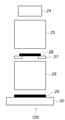
図17は、リソグラフィ工程において使用される投影露光装置の構成例を示す図である。投影露光装置100は、光源(例えば、レーザー)24、照明光学系25、レチクルステージ27、投影光学系28、及び、基板ステージ30を備えている。
FIG. 17 is a diagram showing a configuration example of a projection exposure apparatus used in the lithography process. The
レチクルパターンが形成されたレチクル26は、レチクルステージ27によって保持され位置決めされる。感光剤であるレジストが塗布された基板(例えば、ウエハやガラスプレート)29は、基板ステージ30によって保持され位置決めされる。照明光学系25によって照明されたレチクル26からの光は、投影光学系28を介して基板29上のレジストに投影されて、レジスト内に光学像が形成される。この光学像によってレジストが感光して潜像パターンが形成される。潜像パターンは、レジストが現像装置によって現像されることによってパターン化されて、レジストパターンとなる。通常、光学像又は潜像パターンの形状と現像工程を経て形成されるレジストパターンの形状とは異なる。レジストパターンの形状は、SEMによって計測されうる。
The
図1は、本発明の好適な実施形態におけるレジストパターン形状予測方法の手順を示すフローチャートである。図2は、図1のステップS3で選択される補正モデルを作成する方法の手順を示すフローチャートである。図1に示す処理、及び、図2に示す処理のうちステップS19及びS20を除く処理は、レジストパターン形状シミュレータによって実行されうる。 FIG. 1 is a flowchart showing a procedure of a resist pattern shape prediction method according to a preferred embodiment of the present invention. FIG. 2 is a flowchart showing the procedure of the method for creating the correction model selected in step S3 of FIG. The processing shown in FIG. 1 and the processing shown in FIG. 2 excluding steps S19 and S20 can be executed by a resist pattern shape simulator.
図20は、レジストパターン形状シミュレータの構成例を示す図である。図20に示すレジストパターン形状シミュレータ200は、コンピュータ201にプログラム250をインストールすることによって構成されうる。コンピュータ201は、例えば、CPU210、メモリ(例えば、DRAM、ハードディスク)220、入力部(例えば、キーボード、通信インターフェース、メディアリーダ)230、出力部(例えば、ディスプレイ、メモリ、通信インターフェース)240を含む。プログラム250は、例えば、入力部230によってコンピュータ201に取り込まれてメモリ220に所定形式で書き込まれうる。レジストパターン形状シミュレータ或いはコンピュータ201は、例えば、図17に例示されるような投影露光装置100の一部を構成しうる。この場合において、投影露光装置100のうちコンピュータ201以外の部分の全部又は一部を本体部と定義すれば、コンピュータ201は、該本体部と接続される。
FIG. 20 is a diagram illustrating a configuration example of a resist pattern shape simulator. A resist
図1に示されたレジストパターン形状予測方法を説明する。まず、ステップS1では、任意のレチクルパターン及び露光条件が決定される。この決定は、典型的には、レチクルパターン及び露光条件が入力部230を介してレジストパターン形状シミュレータ200に入力されることによってなされる。図5は、レチクルパターンの一部を例示する図である。
The resist pattern shape prediction method shown in FIG. 1 will be described. First, in step S1, an arbitrary reticle pattern and exposure conditions are determined. This determination is typically made by inputting a reticle pattern and exposure conditions to the resist
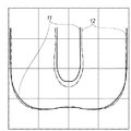
次に、ステップS2では、基準パターン、並びに、該基準パターンの目標寸法及びその評価位置が決定される。この決定は、典型的には、基準パターン、並びに、該基準パターンの目標寸法及びその評価位置が入力部230を介してレジストパターン形状シミュレータ200に入力されることによってなされる。ここで、基準パターンは、レチクルパターンの露光量を決める際に利用する目安となるパターンである。基準パターンは、例えば、図3に例示するようなパターンである。図3において、符号1が付された位置が評価位置の一例である。
Next, in step S2, a reference pattern, a target dimension of the reference pattern, and an evaluation position thereof are determined. This determination is typically made by inputting the reference pattern, the target dimension of the reference pattern and its evaluation position to the resist
次いで、ステップS3では、レジストパターンの形状予測の対象となるレジスト(感光剤)に応じて複数の補正モデルの中から1つの補正モデルが選択される。選択候補となる複数の補正モデルは、図2に示す処理によって形成される。 Next, in step S3, one correction model is selected from a plurality of correction models according to the resist (photosensitive agent) that is the target of resist pattern shape prediction. A plurality of correction models to be selection candidates are formed by the process shown in FIG.
次に、ステップS4では、ステップS2で決定された基準パターンの光学像(投影光学系の像面に形成される像)が計算され、該基準パターンの評価位置において目標寸法を実現する光学スライスレベルが決定される。図4は、光学スライスレベルの決定方法を説明するための図であり、ステップS2で決定された評価位置1における光学像の光強度分布を示している。図4において、符号"2"はステップS2で入力された目標寸法を示し、符号"3"は当該目標寸法2が得られる光学スライスレベルである。
Next, in step S4, an optical image of the reference pattern determined in step S2 (image formed on the image plane of the projection optical system) is calculated, and an optical slice level that realizes a target dimension at the evaluation position of the reference pattern. Is determined. FIG. 4 is a diagram for explaining a method of determining the optical slice level, and shows the light intensity distribution of the optical image at the
次いで、ステップS5では、ステップS1で決定されたレチクルパターン(例えば、図5)を用いた場合に投影光学系28の像面(つまり、基板の表面)に形成される光学像、即ち、光強度分布が計算される。ここで、投影光学系の像面に形成される光学像の計算については、公知の種々の方法を採用しうる。例えば、レチクルパターンが投影光学系の物体面の情報として与えられるとともに該レチクルパターンの照明条件が与えられると、該投影光学系の像面に形成される光学像、即ち、光強度分布を計算することができる。 Next, in step S5, an optical image formed on the image plane of the projection optical system 28 (that is, the surface of the substrate) when the reticle pattern determined in step S1 (for example, FIG. 5) is used, that is, the light intensity. Distribution is calculated. Here, various known methods can be employed for calculating the optical image formed on the image plane of the projection optical system. For example, when a reticle pattern is given as information on the object plane of the projection optical system and illumination conditions for the reticle pattern are given, an optical image formed on the image plane of the projection optical system, that is, a light intensity distribution is calculated. be able to.
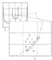
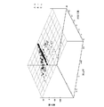
次いで、ステップS6(第2計算工程)では、ステップS5で計算された光強度分布をステップS4で決定された光学スライスレベルで基板面と平行に切断した断面における輪郭形状(以下、光学輪郭形状)が計算される。図6は、図5に示すレチクルパターンを用いた場合に得られる光学輪郭形状を例示する図である。"a"は図5の全体に対応する光学輪郭形状を示す図、"b"は"a"の一部を拡大した図である。"4"は、光学輪郭形状を示している。 Next, in step S6 (second calculation step), a contour shape in a cross section obtained by cutting the light intensity distribution calculated in step S5 parallel to the substrate surface at the optical slice level determined in step S4 (hereinafter, optical contour shape). Is calculated. FIG. 6 is a diagram illustrating an optical contour shape obtained when the reticle pattern shown in FIG. 5 is used. “a” is a diagram showing an optical contour shape corresponding to the whole of FIG. 5, and “b” is an enlarged view of a part of “a”. “4” indicates an optical contour shape.
次に、ステップS7(補正工程の一部)では、光学輪郭形状を構成する光学輪郭点における湾曲率と対数勾配とが該光学輪郭形状の特徴を示す特徴量として計算される。図6を参照して光学輪郭形状の特徴を示す特徴量の計算例を説明する。光学輪郭点5を中心とする光学輪郭形状4に沿った微小領域9を考える。微小領域9における各光学輪郭点が円周上に載るような近似の円を仮想する。光学輪郭点5上における円の曲率半径の逆数を湾曲率と定義する。ここでは、円を例として示すが、楕円関数による湾曲率でもよいし、多項式等のように、2次微係数を算出できる他の関数でもよい。円の中心点と光学輪郭点5とを結ぶ線上の光強度分布の対数を線上の座標で1次微分したものを対数勾配と定義する。対数勾配の方向については、光学輪郭形状の接線の法線や、光強度分布における接面の法線の方向としてもよい。同様にして、微小領域10の中心である光学輪郭点7の湾曲率や対数勾配についても計算することができる。
Next, in step S7 (part of the correction process), the curvature and the logarithmic gradient at the optical contour points constituting the optical contour shape are calculated as feature amounts indicating the characteristics of the optical contour shape. With reference to FIG. 6, an example of calculating the feature amount indicating the feature of the optical contour shape will be described. Consider a
次いで、ステップS8(補正工程の一部)では、計算された湾曲率と対数勾配に応じて補正モデルによって与えられる補正量が計算される。補正量は、値が正の場合も負の場合もありうる。 Next, in step S8 (part of the correction process), a correction amount given by the correction model is calculated according to the calculated curvature and logarithmic gradient. The correction amount may be positive or negative.
次いで、ステップS9(補正工程の一部)では、微小領域の中心の法線ベクトルに基づいて補正方向が決定される。この法線ベクトルは、光学輪郭形状の接線から求めてよいし、計算で得られる光強度分布における接面から求めてもよい。 Next, in step S9 (part of the correction process), the correction direction is determined based on the normal vector at the center of the minute region. This normal vector may be obtained from the tangent of the optical contour shape, or may be obtained from the tangent surface in the light intensity distribution obtained by calculation.
ここで、レジストパターン形状を決定するためのレジストパターン形状計算モデルは、例えば、次式で定義されうる。 Here, the resist pattern shape calculation model for determining the resist pattern shape can be defined by the following equation, for example.
レジストパターンの輪郭点の位置 = 光学輪郭点の位置 + レジストパターン補正量
ステップS10(予測工程)では、計算された補正方向に沿ってステップS8で計算された補正量だけ光学輪郭点の位置を移動させる。光学輪郭形状を構成する微小領域の中心に対応するレジストパターンの輪郭の一点が決定される。即ち、光学輪郭点が補正されてレジストパターンの輪郭点が決定される。例えば、図6の光学輪郭点5に対応するレジストパターンの輪郭点6が決定される。
Position of resist pattern contour point = position of optical contour point + resist pattern correction amount In step S10 (prediction process), the position of the optical contour point is moved by the correction amount calculated in step S8 along the calculated correction direction. Let One point of the contour of the resist pattern corresponding to the center of the minute region constituting the optical contour shape is determined. That is, the optical contour point is corrected to determine the contour point of the resist pattern. For example, the contour point 6 of the resist pattern corresponding to the
ステップS11では、光学輪郭形状を構成する複数の光学輪郭点の全てが処理されたか否かが判断され、未処理の光学輪郭点があれば、処理対象の光学輪郭点が未処理の光学輪郭点に変更されて、処理がステップS7に戻される。 In step S11, it is determined whether or not all of the plurality of optical contour points constituting the optical contour shape have been processed. If there are unprocessed optical contour points, the optical contour points to be processed are unprocessed optical contour points. The process is returned to step S7.
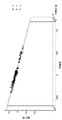
以上の処理によって、ステップS1で決定されたレチクルパターンに対応するレジストパターン形状が決定される。図7には、ステップS6で決定される光学輪郭形状12と、ステップS7〜S11の繰り返しで決定されるレジストパターン形状11とが例示されている。
With the above processing, the resist pattern shape corresponding to the reticle pattern determined in step S1 is determined. FIG. 7 illustrates an
ここでは光強度分布から得られる特徴量(パラメータ)として湾曲率と対数勾配を挙げたが、例えば、多項式の微係数など、光強度分布から得られる他の特徴量(パラメータ)に基づいてレジストパターンを決定してもよい。 Here, the curvature and the logarithmic gradient are given as the feature amount (parameter) obtained from the light intensity distribution, but the resist pattern is based on other feature amount (parameter) obtained from the light intensity distribution, such as a differential coefficient of a polynomial, for example. May be determined.
以上のようなレジストパターン形状予測方法によれば、光学輪郭点の位置に補正量を加算するという単純な方法により、レジストパターンの形状を予測するので、計算時間が短縮される。 According to the resist pattern shape prediction method as described above, the calculation time is shortened because the shape of the resist pattern is predicted by a simple method of adding the correction amount to the position of the optical contour point.
次いで、図2に示す補正モデルの作成について説明する。まず、ステップS13では、補正モデルを作成する対象となるレジストが決定される。この決定は、典型的には、レジスト種類、識別情報又は特性を示す情報が入力部230を介してレジストパターン形状シミュレータ200に入力されることによってなされる。
Next, the creation of the correction model shown in FIG. 2 will be described. First, in step S13, a resist for which a correction model is to be created is determined. This determination is typically made by inputting resist type, identification information, or information indicating characteristics to the resist
次に、ステップS14では、補正モデルを作成するための複数の基本パターンが決定される。また、露光条件、及び、各基本パターンについての複数の評価位置が決定される。この決定は、典型的には、基本パターン、露光条件及び評価位置が入力部230を介してレジストパターン形状シミュレータ200に入力されることによってなされる。
Next, in step S14, a plurality of basic patterns for creating a correction model are determined. Also, the exposure conditions and a plurality of evaluation positions for each basic pattern are determined. This determination is typically made by inputting the basic pattern, exposure conditions, and evaluation position to the resist
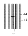
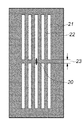
図8、図9、図10に基本パターンA、B、Cが例示されている。基本パターン、露光条件、及び、評価位置は、種々のライン、スペース、ギャップについて評価結果が得られるように決定される。補正モデルは、より多くの基本パターンについて、また、より多くのライン、スペース、ギャップについて評価がなされ、それが反映されることによって精度が向上する。 Basic patterns A, B, and C are illustrated in FIGS. The basic pattern, exposure conditions, and evaluation position are determined so that evaluation results can be obtained for various lines, spaces, and gaps. The correction model is evaluated for more basic patterns and more lines, spaces, and gaps, and the accuracy is improved by reflecting the evaluation.
次に、ステップS15では、基準パターン、並びに、該基準パターンの目標寸法及び評価位置が決定される。基準パターンは、例えば、図3に例示するようなパターンである。図1に示す処理において基本パターン並びに該基準パターンの目標寸法及び評価位置を選択する自由度を高めるためには、より多くの基準パターンについて、また、より多くの目標寸法及び評価位置について評価がなされ、それが補正モデルに反映されるべきである。 Next, in step S15, the reference pattern and the target dimension and evaluation position of the reference pattern are determined. The reference pattern is, for example, a pattern illustrated in FIG. In order to increase the degree of freedom in selecting the basic pattern and the target dimension and evaluation position of the reference pattern in the processing shown in FIG. 1, evaluation is performed for more reference patterns and more target dimensions and evaluation positions. That should be reflected in the correction model.
次に、ステップS16では、ステップS15で決定された基準パターンの光学像が計算され、該基準パターンの評価位置において目標寸法を実現する光学スライスレベルが決定される。この処理の具体例については、ステップS4についての説明と同様である。 Next, in step S16, an optical image of the reference pattern determined in step S15 is calculated, and an optical slice level that realizes a target dimension at the evaluation position of the reference pattern is determined. A specific example of this process is the same as that described for step S4.
次に、ステップS17(第1計算工程の一部)では、ステップS14で決定された基本パターンに従うレチクルを用いた場合に投影光学系の像面に形成される光学像、即ち、光強度分布が計算される。 Next, in step S17 (part of the first calculation step), an optical image formed on the image plane of the projection optical system, that is, the light intensity distribution when the reticle according to the basic pattern determined in step S14 is used. Calculated.
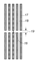
次に、ステップS18では、レチクルパターンと光学輪郭形状との差が計算される。具体的には、まず、ステップS17で計算された光強度分布をステップS16で決定された光学スライスレベルで基板の表面と平行に切断した断面における光学輪郭形状が計算される(第1計算工程)。次いで、ステップS14で決定された評価位置において、基本パターンに従うレチクルパターンの形状と当該基本パターンに従うレチクルパターンを使って投影光学系28の像面に形成される光学像の光学輪郭形状との差が計算される。この差を計算する評価位置は、図8、図9、図10に例示されている。図8に例示される基本パターンは、ライン14及びスペース15を含み、例えば評価位置13でこの差が計算されうる。図9に例示される基本パターンは、ライン17、スペース18、ギャップ(ライン間のギャップ)19を含み、例えば、評価位置16でこの差が計算されうる。図10に例示される基本パターンは、ライン22、スペース21、ギャップ(スペース間のギャップ)23を含み、例えば、評価位置20でこの差が計算されうる。
Next, in step S18, the difference between the reticle pattern and the optical contour shape is calculated. Specifically, first, an optical contour shape in a section obtained by cutting the light intensity distribution calculated in step S17 in parallel with the surface of the substrate at the optical slice level determined in step S16 is calculated (first calculation step). . Next, at the evaluation position determined in step S14, there is a difference between the shape of the reticle pattern according to the basic pattern and the optical contour shape of the optical image formed on the image plane of the projection
次に、ステップS23では、評価位置を含む微小領域を参照領域として、該評価位置における基本パターンの特徴を示す特徴量として湾曲率と対数勾配が計算される。ここで、特徴量の計算は、複数の評価位置のそれぞれについてなされる。特徴量は、湾曲率及び対数勾配に限定されず、他のパラメータでもよい。 Next, in step S23, the curvature ratio and logarithmic gradient are calculated as feature quantities indicating the features of the basic pattern at the evaluation position, using a micro area including the evaluation position as a reference area. Here, the feature amount is calculated for each of the plurality of evaluation positions. The feature amount is not limited to the curvature and the logarithmic gradient, and may be another parameter.
ステップS16〜S23の処理とは、別に、ステップS19〜S21が実行される。 Apart from the processing of steps S16 to S23, steps S19 to S21 are executed.
ステップS19では、露光装置により、基準パターン及び複数の基本パターンを含むレチクルを使って基板が露光され、その後、現像される。これにより、基板上にレジストパターンが形成される。ここで、露光量は、基準パターンの目標寸法に応じて決定される。 In step S19, the exposure apparatus exposes the substrate using a reticle including a reference pattern and a plurality of basic patterns, and then develops the substrate. Thereby, a resist pattern is formed on the substrate. Here, the exposure amount is determined according to the target dimension of the reference pattern.
次に、ステップS20(測定工程、又は、取り込み工程)では、形成されたレジストパターンの形状が測定され、その測定結果がレジストパターン形状シミュレータ200に入力部230を介して取り込まれる。この測定は、例えば、SEM使ってなされうる。測定において評価がなされる評価位置は、図8、図9、図10に例示されている。図8に例示される基本パターンは、ライン14及びスペース15を含み、例えば評価位置13で測定がなされうる。図9に例示される基本パターンは、ライン17、スペース18、ギャップ(ライン間のギャップ)19を含み、例えば、評価位置16で測定がなされうる。図10に例示される基本パターンは、ライン22、スペース21、ギャップ(スペース間のギャップ)23を含み、例えば、評価位置20で測定がなされうる。
Next, in step S20 (measurement process or capture process), the shape of the formed resist pattern is measured, and the measurement result is captured by the resist
ステップS21では、ステップS20における測定結果に基づいて、各基本パターンの各評価位置において、基本パターンに従うレチクルパターンの形状とそれによって形成されたレジストパターンの形状との差が計算される。 In step S21, a difference between the shape of the reticle pattern according to the basic pattern and the shape of the resist pattern formed thereby is calculated at each evaluation position of each basic pattern based on the measurement result in step S20.
次に、ステップS22では、ステップS18とステップS21の計算結果に基づいて、各基本パターンの各評価位置について、光学輪郭形状とレジストパターン形状との差が計算される。この差は、レジストパターン補正量である。ここで、この実施形態では、ステップS18で得られるレチクルパターン形状と光学輪郭形状との差、及び、ステップS21で得られるレチクルパターン形状とレジストパターン形状との差に基づいて、光学輪郭形状とレジストパターン形状との差が計算される。ここでは、レチクルパターンを媒介にして、光学輪郭形状とレジストパターン形状との差を求める例を示した。しかしながら、例えば、基本パターンの対称性を利用してもよい。すなわち、線幅や対向するライン端の幅について、光学輪郭形状を計算し、かつレジストパターン形状を計測し、その差の半分を補正量としてもよい。このように、光学輪郭形状とレジストパターン形状との差を直接計算する方法でもよい。 Next, in step S22, the difference between the optical contour shape and the resist pattern shape is calculated for each evaluation position of each basic pattern based on the calculation results of step S18 and step S21. This difference is a resist pattern correction amount. Here, in this embodiment, based on the difference between the reticle pattern shape obtained in step S18 and the optical contour shape, and the difference between the reticle pattern shape obtained in step S21 and the resist pattern shape, the optical contour shape and the resist The difference from the pattern shape is calculated. Here, an example is shown in which the difference between the optical contour shape and the resist pattern shape is obtained using the reticle pattern as a medium. However, for example, the symmetry of the basic pattern may be used. That is, with respect to the line width and the width of the opposing line end, the optical contour shape may be calculated, the resist pattern shape may be measured, and half of the difference may be used as the correction amount. In this way, a method of directly calculating the difference between the optical contour shape and the resist pattern shape may be used.
ステップS24では、ステップS22とステップS23の計算結果に基づいて、特徴量(湾曲率と対数勾配)と補正量との関係を平面関数で近似して得られる補正モデルが生成される。 In step S24, based on the calculation results of steps S22 and S23, a correction model obtained by approximating the relationship between the feature amount (curvature and logarithmic gradient) and the correction amount with a plane function is generated.
この補正モデルは、補正量を変数Z、湾曲率を変数X、対数勾配を変数Y、係数をa、b、cとすると、次式のような補正モデル(関数)で定義される。この補正モデルは、輪郭形状の輪郭点における湾曲率X及び該輪郭点における該光学像の対数勾配Yの1次の関数で与えられている。 This correction model is defined by a correction model (function) as shown below, where the correction amount is variable Z, the curvature is variable X, the logarithmic gradient is variable Y, and the coefficients are a, b, and c. This correction model is given by a linear function of the curvature X at the contour point of the contour shape and the logarithmic gradient Y of the optical image at the contour point.
Z = aX + bY + c
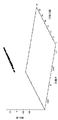
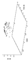
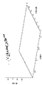
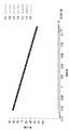
図8のパターンAにおいて、種々の湾曲率と対数勾配の組み合わせのそれぞれについて補正量をプロットすると図11のようになる。図9、図10のパターンB、パターンCにおいて同様にプロットすると、それぞれ図12、図13のようになる。これらの補正量を一緒にプロットして回帰平面関数(回帰関数)を求めたものが、図14、図15である。この回帰平面関数が補正モデルである。平面関数は簡便な式であるため、図1に示す処理において、補正モデルに基づいて光学輪郭形状からレジストパターン形状を計算するために要する時間は短い。
Z = aX + bY + c
In the pattern A of FIG. 8, when the correction amount is plotted for each of various combinations of curvature and logarithmic gradient, FIG. 11 is obtained. Plotting similarly in the patterns B and C of FIGS. 9 and 10, respectively, results in FIGS. 12 and 13, respectively. 14 and 15 show the regression plane function (regression function) obtained by plotting these correction amounts together. This regression plane function is a correction model. Since the plane function is a simple expression, in the process shown in FIG. 1, the time required to calculate the resist pattern shape from the optical contour shape based on the correction model is short.
補正モデルのフィッティングには、例えば、最小二乗法を利用することができる。その精度は、例えば、RMS(Root Mean Square。二乗平均平方根または平均二乗偏差ともいう)で約2nm程度であり、高いフィッティング精度であることがわかる。また、個々のデータのエラー(条件設定差、測定誤差等)に対して影響が少なくなるため、レジストパターン補正モデルの予測精度は高い。 For fitting the correction model, for example, a least square method can be used. The accuracy is, for example, about 2 nm in RMS (Root Mean Square, also referred to as root mean square or mean square deviation), and it can be seen that the fitting accuracy is high. In addition, since the influence on individual data errors (condition setting difference, measurement error, etc.) is reduced, the prediction accuracy of the resist pattern correction model is high.
上述より、補正モデルは平面関数による高速かつ高精度なモデルであると言える。 From the above, it can be said that the correction model is a high-speed and high-accuracy model using a plane function.
図16は、照明の開口率と形状を変化させて、それぞれについて補正モデルを作成して、それらの補正モデルの回帰平面関数(回帰関数)を一緒にプロットした結果である。照明の開口率と形状のバリエーションは、P1からP7の7種類ある。ここで、開口率は0.81から0.85の間で変化させた。リング状の照明形状については、内側の形状を比率で0.47から0.62まで変化させ、外側の形状を比率で0.85から0.93まで変化させている。7種類の補正モデルの回帰平面関数(回帰関数)は、密に重なり合っていることがわかる。つまり、この補正モデルは、投影露光装置の照明条件の変化に対して計算精度の変化が少ないことがわかる。これは、一つの条件で生成した補正モデルが他の照明条件に対しても適用可能であることを意味する。 FIG. 16 shows the results of changing the aperture ratio and shape of the illumination, creating correction models for each, and plotting the regression plane functions (regression functions) of these correction models together. There are seven variations of the aperture ratio and shape of the illumination, from P1 to P7. Here, the aperture ratio was changed between 0.81 and 0.85. As for the ring-shaped illumination shape, the inner shape is changed from 0.47 to 0.62 in proportion, and the outer shape is changed from 0.85 to 0.93 in proportion. It can be seen that the regression plane functions (regression functions) of the seven types of correction models overlap closely. That is, it can be seen that this correction model has a small change in calculation accuracy with respect to a change in illumination conditions of the projection exposure apparatus. This means that a correction model generated under one condition can be applied to other illumination conditions.
上記のレジストパターン形状予測方法及び補正モデルの定義により、高速かつ高精度にレジスト形状予測を行うことができる。したがって、大規模なレチクルパターンについても、それによって形成されるレジストパターンの形状を高速且つ高精度に予測することができる。 By defining the resist pattern shape prediction method and the correction model, the resist shape can be predicted at high speed and with high accuracy. Therefore, even for a large-scale reticle pattern, the shape of the resist pattern formed thereby can be predicted at high speed and with high accuracy.
本発明の好適な実施形態のレジストパターン形状予測方法を用いることで、使用するレジストプロセスについて補正モデルを作成しておけば、実際の露光及び現像を行うことなく露光結果を高速かつ高精度に予測することができる。 By using the resist pattern shape prediction method of the preferred embodiment of the present invention, if a correction model is created for the resist process to be used, the exposure result can be predicted with high speed and high accuracy without performing actual exposure and development. can do.
本発明の好適な実施形態のレジストパターン形状予測方法を用いて、目標とするレジストパターン形状を実現可能なレチクルパターンを生成することができる。例えば、まず、目的とするレジストパターン形状をレチクルパターンとしてレジストパターン形状を予測する。目的とするレジストパターン形状と異なる形状が予測された場合には、異なる部分の光強度を変化させるようにレチクルパターンを変更する。この変更したレチクルパターンに対してレジストパターン形状を予測する。これを目的とするレジストパターン形状が得られるまで繰り返して実行すればよい。 A reticle pattern capable of realizing a target resist pattern shape can be generated using the resist pattern shape prediction method of a preferred embodiment of the present invention. For example, first, a resist pattern shape is predicted using a target resist pattern shape as a reticle pattern. When a shape different from the target resist pattern shape is predicted, the reticle pattern is changed so as to change the light intensity of different portions. A resist pattern shape is predicted for the changed reticle pattern. This may be repeated until a desired resist pattern shape is obtained.
本発明の好適な実施形態のレジストパターン形状予測方法により、レチクルに形成される複数のパターンを用いて目標とする複数のレジストパターン形状を同時に得るための照明条件を探索することができる。例えば、照明形状や開口率が互いに異なる複数の照明条件において、レチクルに形成されるパターンごとに露光量と焦点深度の変化に対するレジストパターン形状の変化を予測する。この予測結果からレチクルに形成される各パターンについて目標とするレジストパターン形状の要求を満たす露光余裕度と焦点深度を計算する。照明条件ごとにレチクルパターンの露光余裕度と焦点深度の共通範囲を評価することにより、レチクルに形成される複数のパターンを用いて目標とする複数のレジストパターン形状を同時に得るための照明条件を探索することができる。 With the resist pattern shape prediction method of a preferred embodiment of the present invention, it is possible to search for illumination conditions for simultaneously obtaining a plurality of target resist pattern shapes using a plurality of patterns formed on a reticle. For example, under a plurality of illumination conditions having different illumination shapes and aperture ratios, a change in the resist pattern shape with respect to a change in exposure amount and depth of focus is predicted for each pattern formed on the reticle. From this prediction result, an exposure margin and a depth of focus that satisfy the requirements of the target resist pattern shape for each pattern formed on the reticle are calculated. Search for illumination conditions to simultaneously obtain multiple target resist pattern shapes using multiple patterns formed on the reticle by evaluating the common range of reticle pattern exposure margin and depth of focus for each illumination condition can do.
更に、上述したレチクルパターン生成方法及び照明条件探索を組み合わせることも可能である。 Further, the above-described reticle pattern generation method and illumination condition search can be combined.
(第2実施形態)
本発明の第2の実施形態では、収差、照度、偏光等の投影露光装置において変更可能なパラメータを条件としてレジストパターン形状予測を行って目標とするレジストパターン形状が得られるパラメータの内容を決定し、その内容に従って投影露光装置を制御する。この一連の処理は自動でなされうる。
(Second Embodiment)
In the second embodiment of the present invention, the resist pattern shape prediction is performed on the condition that parameters that can be changed in the projection exposure apparatus such as aberration, illuminance, and polarization, and the contents of the parameters that can obtain the target resist pattern shape are determined. The projection exposure apparatus is controlled according to the contents. This series of processing can be automatically performed.
図18は、第2の実施形態に係わる投影露光装置の構成例を示す図である。パラメータ決定シミュレータ31は、第1実施形態のレジストパターン形状シミュレータの機能を含む。パラメータ決定シミュレータ31は、当該機能によってレジストパターン形状を予測しながら、投影露光装置300で形成されるレジストパターンが目標とする形状になるように投影露光装置300のパラメータの内容を決定する。パラメータ決定シミュレータ31は、決定したパラメータの内容をコントローラ32に提供し、コントローラ32は、そのパラメータの内容に従って投影露光装置300を動作させる。投影露光装置300のパラメータとしては、例えば、開口率、シグマ、収差、偏光等を挙げることができる。
FIG. 18 is a diagram showing a configuration example of a projection exposure apparatus according to the second embodiment. The
図19は、第2の実施形態の投影露光装置の動作を示すフローチャートである。まず、ステップS25では、コントローラ32は、投影露光装置300において変更可能なパラメータについての情報を収集する。ステップS26では、コントローラ32は、レチクルパターン情報を取得する。ステップS27では、コントローラ32は、レジスト情報を取得する。ここで、レジスト情報には、例えば、補正モデル、基準パターン、光学スライスレベルの情報が含まれうる。
FIG. 19 is a flowchart showing the operation of the projection exposure apparatus of the second embodiment. First, in step S <b> 25, the
ステップS28では、コントローラ32は、ステップS25〜S27で取得した情報をパラメータ決定シミュレータ31に提供する。
In step S28, the
ステップS29では、パラメータ決定シミュレータ31は、投影露光装置300の現時点におけるパラメータの内容を条件として、コントローラ32から提供された情報に基づいてレジストパターン形状を予測する。ステップS30では、パラメータ決定シミュレータ31は、最適な露光量とフォーカスの範囲を計算する。ステップS31では、パラメータ決定シミュレータ31は、現時点におけるパラメータの内容で投影露光装置100を制御して露光を実行した場合に目標とするレジストパターン形状が得られるか否かを判断する。
In step S29, the
ステップS31で目標とするレジストパターン形状が得られないと判断された場合は、ステップS32において、パラメータ決定シミュレータ31は、投影露光装置100のパラメータの値を変更する。その後、ステップS29〜S31が再度実行される。
If it is determined in step S31 that the target resist pattern shape cannot be obtained, the
ステップS31で目標とするレジストパターン形状が得られると判断された場合は、ステップ33では、コントローラ32は、目標とするレジストパターン形状が得られると判断されたパラメータの内容を投影露光装置300に設定する。
If it is determined in step S31 that the target resist pattern shape can be obtained, in
(応用例)
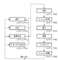
次に上記の投影露光装置100又は300に代表されるようなシミュレータを備えた投影露光装置を利用したデバイス製造方法を説明する。図21は、半導体デバイスの全体的な製造プロセスのフローを示す図である。ステップ1(回路設計)では半導体デバイスの回路設計を行う。ステップ2(レチクル作製)では設計した回路パターンに基づいてレチクル(原版またはマスクともいう)を作製する。一方、ステップ3(ウエハ製造)ではシリコン等の材料を用いてウエハ(基板ともいう)を製造する。ステップ4(ウエハプロセス)は前工程と呼ばれ、上記のレチクルとウエハを用いて、リソグラフィー技術によってウエハ上に実際の回路を形成する。次のステップ5(組み立て)は後工程と呼ばれ、ステップ4によって作製されたウエハを用いて半導体チップ化する工程であり、アッセンブリ工程(ダイシング、ボンディング)、パッケージング工程(チップ封入)等の組み立て工程を含む。ステップ6(検査)ではステップ5で作製された半導体デバイスの動作確認テスト、耐久性テスト等の検査を行う。こうした工程を経て半導体デバイスが完成し、これを出荷(ステップ7)する。
(Application examples)
Next, a device manufacturing method using a projection exposure apparatus provided with a simulator represented by the
図22は、上記ウエハプロセスの詳細なフローを示す図である。ステップ11(酸化)ではウエハの表面を酸化させる。ステップ12(CVD)ではウエハ表面に絶縁膜を成膜する。ステップ13(電極形成)ではウエハ上に電極を蒸着によって形成する。ステップ14(イオン打込み)ではウエハにイオンを打ち込む。ステップ15(CMP)ではCMP工程によって絶縁膜を平坦化する。ステップ16(レジスト処理)ではウエハに感光剤を塗布する。ステップ17(露光)では上記の投影露光装置を用いて、回路パターンが形成されたマスクを介し感光剤が塗布されたウエハを露光してレジストに潜像パターンを形成する。ステップ18(現像)ではウエハ上のレジストに形成された潜像パターンを現像してレジストパターンを形成する。ステップ19(エッチング)ではレジストパターンが開口した部分を通してレジストパターンの下にある層又は基板をエッチングする。ステップ20(レジスト剥離)ではエッチングが済んで不要となったレジストを取り除く。これらのステップを繰り返し行うことによって、ウエハ上に多重に回路パターンを形成する。 FIG. 22 shows a detailed flow of the wafer process. In step 11 (oxidation), the wafer surface is oxidized. In step 12 (CVD), an insulating film is formed on the wafer surface. In step 13 (electrode formation), an electrode is formed on the wafer by vapor deposition. In step 14 (ion implantation), ions are implanted into the wafer. In step 15 (CMP), the insulating film is planarized by a CMP process. In step 16 (resist process), a photosensitive agent is applied to the wafer. In step 17 (exposure), the above-described projection exposure apparatus is used to expose the wafer coated with the photosensitive agent through the mask on which the circuit pattern is formed, thereby forming a latent image pattern on the resist. In step 18 (development), the latent image pattern formed on the resist on the wafer is developed to form a resist pattern. In step 19 (etching), the layer or substrate under the resist pattern is etched through the portion where the resist pattern is opened. In step 20 (resist stripping), the resist that has become unnecessary after etching is removed. By repeating these steps, multiple circuit patterns are formed on the wafer.
Claims (12)
該レチクルパターンとしての基本パターンからの光を該投影光学系によって投影することにより該レジスト内に形成される光学像の輪郭形状を計算する第1計算工程と、
該基本パターンを用いた該露光工程、及び該現像工程を経て形成されたレジストパターンの形状を測定する測定工程と、
前記第1計算工程で計算された輪郭形状と前記測定工程で測定されたレジストパターンの形状との差に応じて決定される補正量と該輪郭形状の特徴量との関係を示す補正モデルを生成する生成工程と、
該レチクルパターンとしての任意のパターンからの光を該投影光学系によって投影することにより該レジスト内に形成される光学像の輪郭形状を計算する第2計算工程と、
前記第2計算工程で計算された光学像の輪郭形状を該輪郭形状の特徴量に応じて該補正モデルによって与えられる補正量に従って補正することにより、該任意のパターンについてのレジストパターンの形状を予測する予測工程と、
を含むことを特徴とするレジストパターン形状予測方法。 A resist pattern shape prediction method for predicting the shape of a resist pattern formed through an exposure step of projecting light from a reticle pattern onto a resist by a projection optical system and exposing the resist, and a development step of developing the resist ,
A first calculation step of calculating a contour shape of an optical image formed in the resist by projecting light from a basic pattern as the reticle pattern by the projection optical system;
A measuring step for measuring the shape of the resist pattern formed through the exposure step using the basic pattern and the developing step;
Generate a correction model indicating the relationship between the correction amount determined according to the difference between the contour shape calculated in the first calculation step and the resist pattern shape measured in the measurement step and the feature amount of the contour shape Generating process to
A second calculation step of calculating a contour shape of an optical image formed in the resist by projecting light from an arbitrary pattern as the reticle pattern by the projection optical system;
The shape of the resist pattern for the arbitrary pattern is predicted by correcting the contour shape of the optical image calculated in the second calculation step according to the correction amount given by the correction model according to the feature amount of the contour shape. A prediction process to
A resist pattern shape prediction method comprising:
該レチクルパターンとしての基本パターンからの光を該投影光学系によって投影することにより該レジスト内に形成される光学像の輪郭形状を計算する第1計算工程と、
該基本パターンを用いた該露光工程、及び該現像工程を経て形成されたレジストパターンの形状を測定した結果を取得する取得工程と、
前記第1計算工程で計算された輪郭形状と前記取得工程で取得されたレジストパターンの形状との差に応じて決定される補正量と該輪郭形状の特徴量との関係を示す補正モデルを生成する生成工程と、
該レチクルパターンとしての任意のパターンからの光を該投影光学系によって投影することにより該レジスト内に形成される光学像の輪郭形状を計算する第2計算工程と、
前記第2計算工程で計算された光学像の輪郭形状を該輪郭形状の特徴量に応じて該補正モデルによって与えられる補正量に従って補正することにより、該任意のパターンについてのレジストパターンの形状を予測する予測工程と、
を含むことを特徴とするレジストパターン形状予測方法。 A resist pattern shape prediction method for predicting the shape of a resist pattern formed through an exposure step of projecting light from a reticle pattern onto a resist by a projection optical system and exposing the resist, and a development step of developing the resist ,
A first calculation step of calculating a contour shape of an optical image formed in the resist by projecting light from a basic pattern as the reticle pattern by the projection optical system;
An acquisition step of acquiring a result of measuring the shape of the resist pattern formed through the exposure step and the development step using the basic pattern;
Generate a correction model indicating the relationship between the correction amount determined according to the difference between the contour shape calculated in the first calculation step and the shape of the resist pattern acquired in the acquisition step and the feature amount of the contour shape Generating process to
A second calculation step of calculating a contour shape of an optical image formed in the resist by projecting light from an arbitrary pattern as the reticle pattern by the projection optical system;
The shape of the resist pattern for the arbitrary pattern is predicted by correcting the contour shape of the optical image calculated in the second calculation step according to the correction amount given by the correction model according to the feature amount of the contour shape. A prediction process to
A resist pattern shape prediction method comprising:
該レチクルパターンとしての基本パターンからの光を該投影光学系によって投影することにより該レジスト内に形成される光学像の輪郭形状を計算する第1計算工程と、
該基本パターンを用いた該露光工程、及び該現像工程を経て形成されたレジストパターンの形状を測定した結果を取得する取得工程と、
前記第1計算工程で計算された輪郭形状と前記取得工程で取得されたレジストパターンの形状との差に応じて決定される補正量と該輪郭形状の特徴量との関係を示す補正モデルを生成する生成工程と、
該レチクルパターンとしての任意のパターンからの光を該投影光学系によって投影することにより該レジスト内に形成される光学像の輪郭形状を計算する第2計算工程と、
前記第2計算工程で計算された光学像の輪郭形状を該輪郭形状の特徴量に応じて該補正モデルによって与えられる補正量に従って補正することにより、該任意のパターンについてのレジストパターンの形状を予測する予測工程と、
を実行させることを特徴とするプログラム。 A program that causes a computer to execute an exposure process for projecting light from a reticle pattern onto a resist by a projection optical system and exposing the resist, and a process for predicting the shape of the resist pattern formed through a development process for developing the resist. In the computer,
A first calculation step of calculating a contour shape of an optical image formed in the resist by projecting light from a basic pattern as the reticle pattern by the projection optical system;
An acquisition step of acquiring a result of measuring the shape of the resist pattern formed through the exposure step and the development step using the basic pattern;
Generate a correction model indicating the relationship between the correction amount determined according to the difference between the contour shape calculated in the first calculation step and the shape of the resist pattern acquired in the acquisition step and the feature amount of the contour shape Generating process to
A second calculation step of calculating a contour shape of an optical image formed in the resist by projecting light from an arbitrary pattern as the reticle pattern by the projection optical system;
The shape of the resist pattern for the arbitrary pattern is predicted by correcting the contour shape of the optical image calculated in the second calculation step according to the correction amount given by the correction model according to the feature amount of the contour shape. A prediction process to
A program characterized by having executed.
該レチクルパターンとしての基本パターンからの光を該投影光学系によって投影することにより該レジスト内に形成される光学像の輪郭形状を計算する第1計算手段と、
該基本パターンを用いた該露光工程、及び該現像工程を経て形成されたレジストパターンの形状を測定した結果を取得する取得手段と、
前記第1計算手段により計算された輪郭形状と前記取得手段により取得されたレジストパターンの形状との差に応じて決定される補正量と該輪郭形状の特徴量との関係を示す補正モデルを生成する生成手段と、
該レチクルパターンとしての任意のパターンからの光を該投影光学系によって投影することにより該レジスト内に形成される光学像の輪郭形状を計算する第2計算手段と、
前記第2計算手段により計算された光学像の輪郭形状を該輪郭形状の特徴量に応じて該補正モデルによって与えられる補正量に従って補正することにより、該任意のパターンについてのレジストパターンの形状を予測する予測手段と、
を含むことを特徴とするコンピュータ。 A computer for predicting the shape of a resist pattern formed through an exposure process of projecting light from a reticle pattern onto a resist by a projection optical system and exposing the resist and a development process of developing the resist,
First calculating means for calculating a contour shape of an optical image formed in the resist by projecting light from a basic pattern as the reticle pattern by the projection optical system;
An acquisition means for acquiring a result of measuring the shape of the resist pattern formed through the exposure step and the development step using the basic pattern;
Generate a correction model indicating the relationship between the correction amount determined according to the difference between the contour shape calculated by the first calculation means and the shape of the resist pattern acquired by the acquisition means and the feature amount of the contour shape Generating means for
Second calculating means for calculating a contour shape of an optical image formed in the resist by projecting light from an arbitrary pattern as the reticle pattern by the projection optical system;
By correcting the contour shape of the optical image calculated by the second calculating means according to the correction amount given by the correction model according to the feature amount of the contour shape, the shape of the resist pattern for the arbitrary pattern is predicted Prediction means to
Including a computer.
請求項10に記載のコンピュータを含む、
ことを特徴とする投影露光装置。 A projection exposure apparatus that projects light from a reticle pattern onto a resist by a projection optical system to expose the resist,
Comprising the computer of claim 10;
A projection exposure apparatus.
請求項11に記載の投影露光装置を用いて基板上のレジストを露光する露光工程と、
該レジストを現像する工程と、
を含むことを特徴とするデバイス製造方法。 A device manufacturing method comprising:
An exposure step of exposing a resist on a substrate using the projection exposure apparatus according to claim 11;
Developing the resist;
A device manufacturing method comprising:
Priority Applications (4)
| Application Number | Priority Date | Filing Date | Title |
|---|---|---|---|
| JP2007047885A JP4328811B2 (en) | 2007-02-27 | 2007-02-27 | Resist pattern shape prediction method, program, and computer |
| TW097106637A TWI447527B (en) | 2007-02-27 | 2008-02-26 | Method for predicting resist pattern shape, computer readable medium storing program for predicting resist pattern shape, and computer for predicting resist pattern shape |
| US12/037,356 US8091048B2 (en) | 2007-02-27 | 2008-02-26 | Method for predicting resist pattern shape, computer readable medium storing program for predicting resist pattern shape, and computer for predicting resist pattern shape |
| KR1020080017568A KR100920857B1 (en) | 2007-02-27 | 2008-02-27 | Method for predicting resist pattern shape, computer readable medium storing program for predicting resist pattern shape, and computer for predicting resist pattern shape |
Applications Claiming Priority (1)
| Application Number | Priority Date | Filing Date | Title |
|---|---|---|---|
| JP2007047885A JP4328811B2 (en) | 2007-02-27 | 2007-02-27 | Resist pattern shape prediction method, program, and computer |
Publications (2)
| Publication Number | Publication Date |
|---|---|
| JP2008211076A JP2008211076A (en) | 2008-09-11 |
| JP4328811B2 true JP4328811B2 (en) | 2009-09-09 |
Family
ID=39717382
Family Applications (1)
| Application Number | Title | Priority Date | Filing Date |
|---|---|---|---|
| JP2007047885A Expired - Fee Related JP4328811B2 (en) | 2007-02-27 | 2007-02-27 | Resist pattern shape prediction method, program, and computer |
Country Status (4)
| Country | Link |
|---|---|
| US (1) | US8091048B2 (en) |
| JP (1) | JP4328811B2 (en) |
| KR (1) | KR100920857B1 (en) |
| TW (1) | TWI447527B (en) |
Families Citing this family (12)
| Publication number | Priority date | Publication date | Assignee | Title |
|---|---|---|---|---|
| JP2010002772A (en) * | 2008-06-20 | 2010-01-07 | Toshiba Corp | Pattern verification-inspection method, method for acquiring distribution of optical image intensity, and program for acquiring distribution of optical image intensity |
| JP2010034402A (en) * | 2008-07-30 | 2010-02-12 | Toshiba Corp | Method of estimating pattern form |
| JP2011049232A (en) * | 2009-08-25 | 2011-03-10 | Renesas Electronics Corp | Exposure device, exposure method, and method for manufacturing semiconductor device |
| JP5539148B2 (en) * | 2010-10-19 | 2014-07-02 | キヤノン株式会社 | Method and program for calculating resist pattern |
| JP5514754B2 (en) * | 2011-02-18 | 2014-06-04 | 株式会社ニューフレアテクノロジー | Inspection apparatus and inspection method |
| US9165095B2 (en) * | 2013-11-15 | 2015-10-20 | Taiwan Semiconductor Manufacturing Company, Ltd. | Target point generation for optical proximity correction |
| US11966167B2 (en) | 2017-12-22 | 2024-04-23 | Asml Netherlands B.V. | Systems and methods for reducing resist model prediction errors |
| JP6996677B2 (en) * | 2018-01-12 | 2022-01-17 | Alitecs株式会社 | Test pattern extraction method and extraction program |
| KR102701616B1 (en) * | 2019-03-25 | 2024-09-04 | 에이에스엠엘 네델란즈 비.브이. | How to determine a pattern in a patterning process |
| TWI762216B (en) * | 2021-02-25 | 2022-04-21 | 力晶積成電子製造股份有限公司 | Method for testing semiconductor pattern |
| JP2023149378A (en) * | 2022-03-31 | 2023-10-13 | 株式会社ニコン | Analysis system and exposure method |
| WO2023189435A1 (en) * | 2022-03-31 | 2023-10-05 | 株式会社ニコン | Analysis system, light exposure method, light exposure apparatus, and device |
Family Cites Families (12)
| Publication number | Priority date | Publication date | Assignee | Title |
|---|---|---|---|---|
| JP3583622B2 (en) | 1998-08-07 | 2004-11-04 | 株式会社東芝 | Resist pattern prediction method |
| US6643616B1 (en) | 1999-12-07 | 2003-11-04 | Yuri Granik | Integrated device structure prediction based on model curvature |
| JP3711083B2 (en) | 2002-04-12 | 2005-10-26 | 株式会社東芝 | Pattern formation method |
| JP2004163472A (en) | 2002-11-08 | 2004-06-10 | Sony Corp | Photomask design method, photomask, and semiconductor device |
| KR100529428B1 (en) * | 2003-02-04 | 2005-11-17 | 동부아남반도체 주식회사 | Method for manufacturing pattern mask by using proximity effect calibrating mask |
| US7588868B2 (en) * | 2004-10-06 | 2009-09-15 | Cadence Design Systems, Inc. | Method and system for reducing the impact of across-wafer variations on critical dimension measurements |
| US7350183B2 (en) * | 2004-11-05 | 2008-03-25 | International Business Machines Corporation | Method for improving optical proximity correction |
| EP1688795A3 (en) * | 2005-01-28 | 2007-12-12 | ASML MaskTools B.V. | Method, computer program and apparatus for improving calibration of resist models used in critical dimension calculation |
| US7488933B2 (en) * | 2005-08-05 | 2009-02-10 | Brion Technologies, Inc. | Method for lithography model calibration |
| KR100958714B1 (en) | 2005-08-08 | 2010-05-18 | 브라이언 테크놀로지스, 인코포레이티드 | System and method for generating a focus-exposure model of a lithography process |
| KR100677995B1 (en) | 2005-12-27 | 2007-02-02 | 동부일렉트로닉스 주식회사 | Control method of photolithography process |
| KR20080021358A (en) * | 2006-09-04 | 2008-03-07 | 삼성전자주식회사 | How to create a reticle |
-
2007
- 2007-02-27 JP JP2007047885A patent/JP4328811B2/en not_active Expired - Fee Related
-
2008
- 2008-02-26 US US12/037,356 patent/US8091048B2/en not_active Expired - Fee Related
- 2008-02-26 TW TW097106637A patent/TWI447527B/en not_active IP Right Cessation
- 2008-02-27 KR KR1020080017568A patent/KR100920857B1/en not_active Expired - Fee Related
Also Published As
| Publication number | Publication date |
|---|---|
| US8091048B2 (en) | 2012-01-03 |
| US20080209386A1 (en) | 2008-08-28 |
| TWI447527B (en) | 2014-08-01 |
| KR100920857B1 (en) | 2009-10-09 |
| KR20080079623A (en) | 2008-09-01 |
| JP2008211076A (en) | 2008-09-11 |
| TW200900872A (en) | 2009-01-01 |
Similar Documents
| Publication | Publication Date | Title |
|---|---|---|
| JP4328811B2 (en) | Resist pattern shape prediction method, program, and computer | |
| TWI334961B (en) | Apparatus, method and computer program product for performing a model based optical proximity correction factoring neighbor influence | |
| JP2020126279A (en) | Separation of contributions to metrology data | |
| JP5149307B2 (en) | Scanner-based optical proximity correction system and method of use | |
| TWI475334B (en) | Integration of lithography devices and reticle optimization process with multiple patterning processes | |
| JP4351928B2 (en) | Mask data correction method, photomask manufacturing method, and mask data correction program | |
| KR101757743B1 (en) | Flare correction method and method for fabricating EUV(Extreme Ultra Violet) mask | |
| KR20190139967A (en) | Method of predicting the yield of the device manufacturing process | |
| TWI467344B (en) | Method of determining exposure parameter, exposure method, method of manufacturing device and recording medium | |
| JP2008122929A (en) | How to create a simulation model | |
| JP2008166777A (en) | Lithographic apparatus and device manufacturing method | |
| KR20210078551A (en) | Methods for determining the root cause of events in a semiconductor manufacturing process and for monitoring the semiconductor manufacturing process | |
| TW201821899A (en) | Target optimization method | |
| US8029954B2 (en) | Exposure method and memory medium storing computer program | |
| CN109656093B (en) | Method for designing layout of photomask and method for manufacturing photomask | |
| JP2020534558A (en) | Patterning process control method, device manufacturing method | |
| KR102390216B1 (en) | Method and apparatus for pattern fidelity control | |
| TWI902374B (en) | Inspection data filtering systems and methods | |
| JP2010156866A (en) | Feature-quantity extracting method, test pattern selecting method, resist model creating method, and designed-circuit-pattern verifying method | |
| US20250199419A1 (en) | Methods of metrology and associated devices | |
| JP5437124B2 (en) | Charged particle beam drawing method and charged particle beam drawing apparatus | |
| JP2010251500A (en) | Semiconductor device manufacturing method and exposure condition determining program | |
| JP4727288B2 (en) | Method and program for optimizing a design formed on a substrate | |
| JP6338368B2 (en) | Method for evaluating pattern optical image | |
| KR20090069095A (en) | Semiconductor device formation method |
Legal Events
| Date | Code | Title | Description |
|---|---|---|---|
| A977 | Report on retrieval |
Free format text: JAPANESE INTERMEDIATE CODE: A971007 Effective date: 20090224 |
|
| A131 | Notification of reasons for refusal |
Free format text: JAPANESE INTERMEDIATE CODE: A131 Effective date: 20090302 |
|
| A521 | Request for written amendment filed |
Free format text: JAPANESE INTERMEDIATE CODE: A523 Effective date: 20090430 |
|
| TRDD | Decision of grant or rejection written | ||
| A01 | Written decision to grant a patent or to grant a registration (utility model) |
Free format text: JAPANESE INTERMEDIATE CODE: A01 Effective date: 20090605 |
|
| A01 | Written decision to grant a patent or to grant a registration (utility model) |
Free format text: JAPANESE INTERMEDIATE CODE: A01 |
|
| A61 | First payment of annual fees (during grant procedure) |
Free format text: JAPANESE INTERMEDIATE CODE: A61 Effective date: 20090615 |
|
| FPAY | Renewal fee payment (event date is renewal date of database) |
Free format text: PAYMENT UNTIL: 20120619 Year of fee payment: 3 |
|
| R150 | Certificate of patent or registration of utility model |
Ref document number: 4328811 Country of ref document: JP Free format text: JAPANESE INTERMEDIATE CODE: R150 Free format text: JAPANESE INTERMEDIATE CODE: R150 |
|
| FPAY | Renewal fee payment (event date is renewal date of database) |
Free format text: PAYMENT UNTIL: 20120619 Year of fee payment: 3 |
|
| FPAY | Renewal fee payment (event date is renewal date of database) |
Free format text: PAYMENT UNTIL: 20130619 Year of fee payment: 4 |
|
| LAPS | Cancellation because of no payment of annual fees |