JP4305286B2 - Computer system - Google Patents
Computer system Download PDFInfo
- Publication number
- JP4305286B2 JP4305286B2 JP2004167936A JP2004167936A JP4305286B2 JP 4305286 B2 JP4305286 B2 JP 4305286B2 JP 2004167936 A JP2004167936 A JP 2004167936A JP 2004167936 A JP2004167936 A JP 2004167936A JP 4305286 B2 JP4305286 B2 JP 4305286B2
- Authority
- JP
- Japan
- Prior art keywords
- data
- data transfer
- memory
- signal
- controller
- Prior art date
- Legal status (The legal status is an assumption and is not a legal conclusion. Google has not performed a legal analysis and makes no representation as to the accuracy of the status listed.)
- Expired - Fee Related
Links
Images


Description
本発明は、パーソナルコンピュータ、ワークステーション、オフィスコンピュータ等の計算機システムにおけるメモリシステム、特に大容量メモリシステムに関する。 The present invention relates to a memory system in a computer system such as a personal computer, a workstation, an office computer, and more particularly to a large capacity memory system.
最近のプロセッサの急激な性能上昇に対し、メモリサブシステムにはプロセッサが要求する高いバンド幅を満たすためにより大きなデータ幅とより高速な動作が要求されている。それに加えて、メモリ容量を可能な限り大きくとりたいという要求もある。 In response to the recent rapid increase in performance of processors, the memory subsystem is required to have a larger data width and higher speed operation in order to satisfy the high bandwidth required by the processor. In addition, there is also a demand to increase the memory capacity as much as possible.
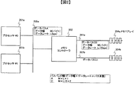
図2は計算機システム構成の一例である。以下では図中の番号で201a,201bのように英小文字のサフィックスがついているものは複数あるもののうちの1つ要素を示し、サフィックスを含まないで記した場合はすべての要素を示しているものとする。また、要素の名称でデータバスA、B、Cに関してデータバスC0、C1のように直後に数字を記しているものは複数あるもののうちの1つの要素を示し、数字を含まないで記した場合はすべての要素を示しているものとする。 FIG. 2 shows an example of a computer system configuration. In the following, numbers in the figure that have a lowercase suffix such as 201a and 201b indicate one element of multiple elements, and all elements are described without a suffix And Also, in the case of the data buses A, B, and C with the element names, a number written immediately after, such as the data buses C0 and C1, indicates one element among a plurality of items, and is written without including a number Indicates all elements.
本計算機システムは、プロセッサ(201)とデータバスA(205)を介して接続しているメモリコントローラ(202)と、メモリコントローラとメモリアレイ(204)を接続する複数のデータバスC(207)から構成される。図ではプロセッサとメモリアレイのバス幅は同じM(バイト)であるが、データレートはプロセッサがL(bps)であるのに対し、メモリアレイはその半分のL/2(bps)でしか動作できないために、データバスCをC0とC1の2本用意することでデータバスAとデータバスCでバンド幅を揃えている。 This computer system includes a memory controller (202) connected to the processor (201) via the data bus A (205), and a plurality of data buses C (207) connecting the memory controller and the memory array (204). Composed. In the figure, the bus width of the processor and the memory array is the same M (bytes), but the data rate is L (bps) for the processor, whereas the memory array can only operate at half that L / 2 (bps). Therefore, by preparing two data buses C0 and C1, the data bus A and the data bus C have the same bandwidth.
データレートがL(bps)で動作可能なメモリアレイが登場した場合の構成を図3に示す。図2との相違点は、データバスCのデータレートが2倍のL(bps)になったこと、データバスCに接続可能なメモリアレイの数が減ったことである。データバスAとデータバスCのデータ幅・データレートが等しくなるので、データバスCの本数が1本だけでこの計算機システムのバンド幅は揃う。しかし、高速となったデータバスCのインターフェースの電気的特性より負荷数に限界が生じ、データバスCに接続可能なメモリアレイの数が減るのでデータバスが1本の場合はメモリ容量が図2の構成に比べて少なくなる。図2と図3のメモリコントローラが同一のLSIパッケージであるとデータバスCをもう1本追加する余裕があり、データバスCを2本用意してメモリ容量を稼ぐことになる。このとき、メモリアレイ側はプロセッサ側の2倍のバンド幅を有しているが、プロセッサ側のバンド幅が変わっていないので、データバスAがボトルネックとなりシステム全体の最大スループットには影響していない。ただし、メモリへのアクセスパターンによっては実効スループットおよび平均アクセス時間は向上する場合がある。 FIG. 3 shows a configuration when a memory array that can operate at a data rate of L (bps) appears. The difference from FIG. 2 is that the data rate of the data bus C has doubled L (bps), and the number of memory arrays connectable to the data bus C has decreased. Since the data width and the data rate of the data bus A and the data bus C are equal, the bandwidth of this computer system is equal only with one data bus C. However, the number of loads is limited due to the electrical characteristics of the interface of the data bus C that has become high-speed, and the number of memory arrays that can be connected to the data bus C is reduced. Compared to the configuration of If the memory controllers of FIGS. 2 and 3 are the same LSI package, there is room to add another data bus C, and two data buses C are prepared to increase the memory capacity. At this time, the memory array side has twice the bandwidth of the processor side, but since the bandwidth on the processor side has not changed, the data bus A becomes a bottleneck, affecting the maximum throughput of the entire system. Absent. However, the effective throughput and average access time may be improved depending on the access pattern to the memory.
プロセッサ側の要求バンド幅が図3の2倍になった構成を図4に示す。図3との相違点はメモリコントローラにデータバスA1を接続したことである。この状態ではデータバスAとデータバスCにおいてデータ幅・データレート・バスの本数が等しいため、バンド幅はプロセッサ側とメモリ側とで釣り合う。ただし、接続できるメモリアレイの数がデータバスCの本数で制限されているためプロセッサのスループットに対してメモリの大容量化が難しく、大容量のメモリを必要とするアプリケーションには不向きである。この構成図に対して、さらにメモリ容量を確保するために行われてきた手法は、次の三つに分類できる。 FIG. 4 shows a configuration in which the required bandwidth on the processor side is double that of FIG. The difference from FIG. 3 is that the data bus A1 is connected to the memory controller. In this state, the data bus A and the data bus C have the same data width, data rate, and number of buses, so the bandwidth is balanced between the processor side and the memory side. However, since the number of memory arrays that can be connected is limited by the number of data buses C, it is difficult to increase the memory capacity with respect to the throughput of the processor, which is not suitable for applications that require a large capacity memory. With respect to this configuration diagram, the techniques that have been performed to further secure the memory capacity can be classified into the following three types.
一つ目は、メモリコントローラに使用されるLSIパッケージにピン数の多いものを使用して、メモリアレイ側に接続できるデータバスの本数を増やすことである。ただし、多ピン型のLSIパッケージは主流のLSIパッケージに比べコストが高いことや、多ピン型といってもその数には限界があることが問題点である。1998年現在、信号ピン数が400ピンあたりが主流であり、信号ピン数と電源ピン数の比が約2:1とするとパッケージには600ピンクラスが用いられている。1000ピンクラスのパッケージも存在するがまだまだ高価である。 The first is to increase the number of data buses that can be connected to the memory array side by using an LSI package having a large number of pins for the memory controller. However, the problem is that multi-pin type LSI packages are more expensive than mainstream LSI packages, and the number of multi-pin type LSI packages is limited. As of 1998, the number of signal pins is around 400, and if the ratio of the number of signal pins to the number of power supply pins is about 2: 1, the 600 pin class is used for the package. There are 1000 pin class packages, but they are still expensive.
二つ目は、データバスCに接続するメモリアレイの数を増やすことである。そのためには、データバスCのインターフェイスに特開平7−202947(出願人:日立製作所)で開示されている高速多負荷接続可能なSSTLインターフェイスを用い、かつそのデータ転送方式に特開平10−293635(出願人:日立製作所)に記載されているソース同期転送方式をもちいることである。その構成を図5に示す。図4との相違点は、メモリサブコントローラとメモリアレイの接続形態がリング状となり、1:2のマルチプレクサ(208)(以降MUX)を介して接続されていることである。MUXの効果は、前述の特願平8−145431で示されているように、メモリアクセスの書き込みと読み出し動作によりその転送方向を変更し、メモリサブコントローラに必要とされるピン数を約半分に削減することである。SSTLインターフェイスとはバスに接続している負荷のスタブにシリーズ抵抗を挿入しバスラインへの反射を抑えるインターフェイスであり、ソース同期転送方式とはデータ転送の供給元がデータ信号とともにソースクロック信号を送信し、受信側でソースクロック信号を用いて受信データ信号をラッチするデータ転送方式である。従来のシステムクロック信号でデータ転送を行う同期転送方式とは異なり、ソース同期転送方式では転送するデータ信号とソースクロック信号が平行して走っているためその伝播遅延時間がほぼ等しく、セットアップ・ホールド時間等のタイミング設計時にバスの配線長による伝播遅延時間をほとんど無視できるので、高速データ転送が容易となる。上記の2つを組み合わせることで多負荷接続バスにおける高速データ転送が可能となり、高速動作でありながらメモリ容量を増やすことができる。この場合においてもメモリ容量はメモリコントローラに接続できるデータバスCの本数によって決定されるため、さらにメモリ容量を増やそうとするとメモリコントローラのLSIパッケージのピン数を増やすしかない。 The second is to increase the number of memory arrays connected to the data bus C. For this purpose, the SSTL interface disclosed in Japanese Patent Laid-Open No. 7-202947 (Applicant: Hitachi) is used for the interface of the data bus C, and the data transfer method is Japanese Patent Laid-Open No. 10-293635 ( (Applicant: Hitachi, Ltd.) using the source synchronous transfer method. The configuration is shown in FIG. The difference from FIG. 4 is that the connection form of the memory sub-controller and the memory array is ring-shaped and connected via a 1: 2 multiplexer (208) (hereinafter referred to as MUX). As shown in Japanese Patent Application No. 8-145431, the effect of MUX is to change the transfer direction by memory access write and read operations, and halve the number of pins required for the memory sub-controller. It is to reduce. The SSTL interface is an interface that suppresses reflection to the bus line by inserting a series resistor in the stub of the load connected to the bus. The source synchronous transfer method transmits the source clock signal along with the data signal from the data transfer source. The data transfer method latches the received data signal using the source clock signal on the receiving side. Unlike the conventional synchronous transfer method that transfers data using the system clock signal, the source synchronous transfer method runs in parallel because the data signal to be transferred and the source clock signal run in parallel, and the setup hold time Since the propagation delay time due to the bus wiring length can be almost ignored at the time of timing design, etc., high-speed data transfer is facilitated. Combining the above two enables high-speed data transfer on a multi-load connection bus, and the memory capacity can be increased while operating at high speed. Even in this case, the memory capacity is determined by the number of data buses C that can be connected to the memory controller. Therefore, if the memory capacity is further increased, the number of pins of the LSI package of the memory controller must be increased.
三つ目は、データバスCの本数を増えたように見せかけることである。その構成を図6に示す。図4との相違点は、メモリコントローラとメモリアレイ間に1:NのMUX(209)を接続して、見かけ上のバスの本数を増やしていることである。そのため、メモリ容量はMUX使用前のN倍となる。しかし、メモリアレイに接続されているバスの本数とメモリの容量は増えているにもかかわらず、メモリコントローラに接続されているバスの本数は変わっていないためにデータバスCのバンド幅は変わらない。そのうえ、途中に1:NのMUXを挿入したことで、このMUXの切り替えにかかる時間がオーバーヘッドとなり実効スループットが低下するという問題もある。また、メモリアレイが空間的に広がるため、メモリコントローラとメモリアレイ間での高速データ転送が難しくなり、メモリコントローラとMUX間もしくはMUXとメモリアレイ間にデータバッファを設置する必要も生じる。 The third is to make it appear that the number of data buses C has increased. The configuration is shown in FIG. The difference from FIG. 4 is that a 1: N MUX (209) is connected between the memory controller and the memory array to increase the number of apparent buses. Therefore, the memory capacity is N times before using MUX. However, although the number of buses connected to the memory array and the memory capacity have increased, the number of buses connected to the memory controller has not changed, so the bandwidth of the data bus C does not change. . In addition, since a 1: N MUX is inserted in the middle, there is a problem that the time required for switching the MUX becomes an overhead and the effective throughput is lowered. In addition, since the memory array is spatially widened, high-speed data transfer between the memory controller and the memory array becomes difficult, and it is necessary to install a data buffer between the memory controller and the MUX or between the MUX and the memory array.
一方、データ転送にソース同期転送方式を用いることで高速データ転送を実現し、バンド幅を向上させることが可能となる。ソース同期転送方式ではデータ転送装置間のデータ信号とソースクロック信号の伝播遅延時間を等しくさえすれば、データ転送装置間の伝送路における伝播遅延時間すなわちデータ転送装置間の距離に左右されずに高速なデータ転送が可能である。データ転送も1サイクル転送に限らずマルチサイクル転送可能となる。ただし、Nサイクル転送を行う場合にはデータの伝播遅延時間Tdが
(N−1)×(1マシンサイクル時間) < Td < N×(1マシンサイクル時間)にあることを保証する必要があり、データ転送装置間のデータの伝播遅延時間に合わせたインターフェイス回路をデータ転送装置内に作成し、Nサイクル転送を実現している。データ転送装置内のインターフェイス回路は外部の伝送路に合わせて作成した唯一のものであり、外部の伝送路の変更には従順に対応できない場合が多い。
On the other hand, by using the source synchronous transfer method for data transfer, high-speed data transfer can be realized and the bandwidth can be improved. In the source synchronous transfer method, as long as the propagation delay time of the data signal between the data transfer devices and the source clock signal is equal, the transmission delay time in the transmission path between the data transfer devices, that is, the high speed is not affected by the distance between the data transfer devices. Data transfer is possible. Data transfer is not limited to 1-cycle transfer, and multi-cycle transfer is possible. However, when performing N cycle transfer, the data propagation delay time Td is
It is necessary to ensure that (N-1) × (1 machine cycle time) <Td <N × (1 machine cycle time), and the interface circuit matched to the data propagation delay time between data transfer devices It is created in the transfer device to realize N cycle transfer. The interface circuit in the data transfer apparatus is the only one created in accordance with the external transmission path, and in many cases, the change of the external transmission path cannot be compliantly followed.
従来の計算機システム構成では上記に示したように次の問題点がある。
(1) メモリコントローラのピン数を増やしてデータバスCの本数を増大させようとするとメモリコントローラのコスト増を招く。
(2) データバスCの本数を見かけ上増やしてメモリ容量を増やすことは可能であるが、バンド幅が向上しない。
(3) (2)において、見かけ上のデータバスCをMUXで接続した場合は、MUXの切り替え時間がオーバーヘッドとなり実効スループットが低下する。
(4) ソース同期転送方式においては、データの伝播遅延時間に合わせて転送サイクル数が決定し、そのサイクル数に合わせたインターフェイス回路をデータ転送装置内に作成する必要がある。
The conventional computer system configuration has the following problems as described above.
(1) Increasing the number of pins of the memory controller to increase the number of data buses C increases the cost of the memory controller.
(2) Although it is possible to increase the memory capacity by apparently increasing the number of data buses C, the bandwidth is not improved.
(3) In (2), when the apparent data bus C is connected by MUX, the switching time of MUX becomes overhead and the effective throughput is lowered.
(4) In the source synchronous transfer method, the number of transfer cycles is determined according to the propagation delay time of data, and an interface circuit corresponding to the number of cycles needs to be created in the data transfer apparatus.
本発明の目的は、
(1) 高速データ転送可能なソース同期転送方式を複数のデータ転送装置に採用してバンド幅を向上させたメモリサブシステム
(2) メモリを大容量化し、かつコスト増を招くことなくバンド幅を向上させたメモリサブシステム
(3) データ転送にソース同期転送方式を採用し、データ転送の最小転送サイクルを保証するバッファを具備し、データの伝送路による最小伝播遅延時間に左右されずにマルチサイクルデータ転送を実現するデータ転送装置を提供することにある。
The purpose of the present invention is to
(1) Memory subsystem with improved bandwidth by adopting source synchronous transfer method capable of high-speed data transfer to multiple data transfer devices
(2) Memory subsystem with increased memory capacity and improved bandwidth without increasing costs
(3) Data that uses a source synchronous transfer method for data transfer, has a buffer that guarantees the minimum transfer cycle of data transfer, and realizes multi-cycle data transfer regardless of the minimum propagation delay time by the data transmission path It is to provide a transfer device.
上記目的を達成するために、メモリコントローラとメモリアレイ間に1つまたは2つ以上の複数のメモリサブコントローラを設け、メモリコントローラとメモリサブコントローラの間を第1のデータバスで接続し、メモリサブコントローラとメモリアレイ間を1本もしくは2本以上の複数の第2のデータバスで接続し、第1のデータバスおよび第2のデータバスでソース同期転送方式で高速データ転送を行うようにして、バンド幅を向上させたメモリサブシステムを構築する。 In order to achieve the above object, one or more memory sub-controllers are provided between the memory controller and the memory array, and the memory controller and the memory sub-controller are connected by a first data bus. The controller and the memory array are connected by one or more second data buses, and high-speed data transfer is performed by the source synchronous transfer method using the first data bus and the second data bus. Build a memory subsystem with improved bandwidth.
また、第1のデータバスおよび第2のデータバスはソース同期転送方式でデータ転送を行うようにし、さらに、メモリサブコントローラとメモリコントローラのバスインターフェイス部にはデータレート変換手段およびデータ幅変換手段のいずれか一方もしくは両方を備えた。 The first data bus and the second data bus perform data transfer by the source synchronous transfer method, and further, the data interface conversion unit and the data width conversion unit are provided in the bus interface unit of the memory sub-controller and the memory controller. Either one or both were provided.
1つのメモリサブコントローラに接続している第1のデータバスのデータレートを大きくして、第1のデータバスのバンド幅が該メモリサブコントローラに接続している第2のデータバスのバンド幅の総和に等しくなるように変更することにより、コスト増を招くことなく高スループットかつ大容量メモリサブシステムを構築する。 The data rate of the first data bus connected to one memory sub-controller is increased so that the bandwidth of the first data bus is equal to the bandwidth of the second data bus connected to the memory sub-controller. By changing to be equal to the sum, a high-throughput and large-capacity memory subsystem is constructed without increasing costs.
また、メモリコントローラに接続している第1のデータバスのデータ幅を小さくし、データレート大きくして、第1のデータバスのバンド幅を該メモリコントローラに接続している第3のデータバスのバンド幅と等しくなるように変更することにより、メモリコントローラのLSIパッケージにかかるコストを削減し、かつプロセッサの要求バンド幅をもつ大容量メモリサブシステムを構築する。 Further, the data width of the first data bus connected to the memory controller is reduced, the data rate is increased, and the bandwidth of the first data bus is connected to that of the third data bus connected to the memory controller. By changing to be equal to the bandwidth, the cost for the LSI package of the memory controller is reduced, and a large-capacity memory subsystem having the required bandwidth of the processor is constructed.
また、ソース同期転送を行うメモリコントローラとメモリサブコントローラのデータ転送I/F部にバッファをN段具備することで、データ転送の最小転送サイクルを保証し、第1のデータバスおよび第2のデータバスにおいてNサイクルデータ転送を実現するメモリサブシステムを構築する。 Further, by providing N stages of buffers in the data transfer I / F section of the memory controller and the memory sub-controller that perform source synchronous transfer, the minimum transfer cycle of data transfer is guaranteed, and the first data bus and the second data A memory subsystem that implements N-cycle data transfer on the bus is constructed.
本発明は、複数のプロセッサとデータバスAを介して接続しているメモリコントローラとメモリアレイからなる計算機システムにおいて、メモリコントローラとメモリアレイ間に1つまたは2つ以上の複数のメモリサブコントローラを設け、1つのメモリサブコントローラとメモリコントローラ間をデータバスBで接続し、メモリサブコントローラとメモリアレイを1つまたは2つ以上の複数のデータバスCで接続し、データバスBおよびデータバスCはソース同期転送を行うようにし、さらにメモリサブコントローラとメモリコントローラのデータバスインターフェイス部にはデータレート変換回路およびデータ幅変換回路のいずれか一方もしくは両方を備え、データバスBのデータ幅を大きくさせないでデータレートを大きくして、データバスBのバンド幅がデータバスCのバンド幅の総和に等しくなるようにデータバスBのデータ幅およびデータレートを決定することにより、最大スループットを低下させることなくメモリを大容量化し、かつコスト増を招くことなくバンド幅を向上させることが可能である。 The present invention provides a computer system comprising a memory controller and a memory array connected to a plurality of processors via a data bus A, and one or more memory sub-controllers are provided between the memory controller and the memory array. One memory sub-controller and a memory controller are connected by a data bus B, and the memory sub-controller and the memory array are connected by one or more data buses C. The data bus B and the data bus C are sources. The data bus interface unit of the memory sub-controller and the memory controller is provided with one or both of a data rate conversion circuit and a data width conversion circuit so that the data width of the data bus B is not increased. Increase the rate, By determining the data width and data rate of the data bus B so that the bandwidth of the bus B becomes equal to the sum of the bandwidths of the data bus C, the capacity of the memory is increased and the cost is increased without decreasing the maximum throughput. It is possible to improve the bandwidth without incurring the problem.
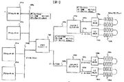
本発明の一実施例を図1、図7〜12を用いて説明する。図1において、複数のプロセッサ(101)とデータバスA(105)を介して接続しているメモリコントローラ(102)とメモリアレイ(104)との中間に存在するメモリサブコントローラ(103)、メモリサブコントローラとメモリコントローラを接続するデータバスB(106)、メモリサブコントローラとメモリアレイを接続する複数のデータバスC(107)から構成する。メモリコントローラにはメモリアレイ側に2本のデータバスをもち、それぞれ1つのメモリサブコントローラ(103a〜b)にデータバスB(106a〜b)を介して接続され、該メモリサブコントローラにはメモリアレイに対するバスを2本ずつもち、データバスCを介してメモリアレイに接続される。ここで、メモリサブコントローラ103aからメモリアレイ104aおよびメモリアレイ104bまでの構成とメモリサブコントローラ103bからメモリアレイ104cおよびメモリアレイ104dまでの構成は全く同じである。そのため、本実施例では片方のメモリサブコントローラについて説明するが、もう一方のメモリサブコントローラについても同様のことが言える。 An embodiment of the present invention will be described with reference to FIGS. 1 and 7 to 12. In FIG. 1, a memory sub-controller (103), a memory sub-memory that exists between a memory controller (102) and a memory array (104) connected to a plurality of processors (101) via a data bus A (105). A data bus B (106) connecting the controller and the memory controller and a plurality of data buses C (107) connecting the memory sub-controller and the memory array are included. The memory controller has two data buses on the memory array side, and is connected to one memory sub-controller (103a-b) via a data bus B (106a-b), respectively. Are connected to the memory array via the data bus C. Here, the configuration from the memory sub-controller 103a to the memory array 104a and the memory array 104b is exactly the same as the configuration from the memory sub-controller 103b to the memory array 104c and the memory array 104d. Therefore, in this embodiment, one memory sub-controller will be described, but the same can be said for the other memory sub-controller.
データバスC0およびC1は同じデータレートL(bps)であり、同じデータ幅M(バイト)であるので、データバスC0およびC1の各バスのバンド幅は(L×M)である。データバスB0のデータレートはデータバスCの2倍の2L(bps)であるが、データ幅はデータバスC0およびC1と等しいM(バイト)であるので、データバスB0のバンド幅は(2×L×M)である。このようにデータバスBのデータ幅はそのままでデータレートを2倍にすることで、データバスBのバンド幅を2倍にする方法を説明する。 Since the data buses C0 and C1 have the same data rate L (bps) and the same data width M (bytes), the bandwidth of each bus of the data buses C0 and C1 is (L × M). The data rate of the data bus B0 is 2L (bps), which is twice that of the data bus C. However, since the data width is M (bytes) equal to the data buses C0 and C1, the bandwidth of the data bus B0 is (2 × L × M). A method of doubling the bandwidth of the data bus B by doubling the data rate without changing the data width of the data bus B will be described.
図7は図1のメモリサブコントローラ(103)のブロック図である。301〜315はメモリサブコントローラを構成する要素および信号線である。401〜406はメモリコントローラとのインターフェイス信号であり、この信号線を用いてメモリアレイに対する制御信号を送信する。501〜505はメモリコントローラとのインターフェイス信号であり、この信号線を用いてデータ信号を送受信する。601〜605はデータバスC0のインターフェイス信号であり、701〜705はデータバスC1のインターフェイス信号である。601〜605と701〜705は接続先のバスが異なるだけで信号線の種類・意味・タイミングは同一である。
FIG. 7 is a block diagram of the memory sub-controller (103) of FIG.
図中のメモリサブコントローラは、エッジトリガタイプフリップフロップ(301)、入力バッファ(302)、出力バッファ(303)、2:1セレクタ(304)、2:1セレクタへのセレクト信号(305)から構成される。エッジトリガタイプフリップフロップのトリガクロック信号はシステムクロック信号(T0)、もしくはバスから受信したソース同期転送用のソースクロック信号である。図中のT14、T24、およびT34はシステムクロック信号(T0)からそれぞれ1/4相、2/4相、3/4相遅れた信号であり、ソース同期転送用のソースクロック信号に用いる。 The memory sub-controller in the figure is composed of an edge trigger type flip-flop (301), an input buffer (302), an output buffer (303), a 2: 1 selector (304), and a select signal (305) to the 2: 1 selector. Is done. The trigger clock signal of the edge trigger type flip-flop is a system clock signal (T0) or a source clock signal for source synchronous transfer received from the bus. T14, T24, and T34 in the figure are signals delayed by 1/4 phase, 2/4 phase, and 3/4 phase, respectively, from the system clock signal (T0), and are used as source clock signals for source synchronous transfer.
メモリコントローラとのインターフェイスは、メモリコントローラからメモリサブコントローラへ送信されるアドレス信号(401)、制御コマンド信号(404)、アドレス信号に対するソースクロック信号(402と403)、制御コマンド信号に対するソースクロック信号(405と406)、双方向のデータ信号(503)、受信データに対するソースクロック信号(501と502)、送信データに対するソースクロック信号(504と505)から構成される。ソースクロックが2本ずつある理由は後で述べる。 The interface with the memory controller includes an address signal (401) transmitted from the memory controller to the memory sub-controller, a control command signal (404), a source clock signal for the address signal (402 and 403), a source clock signal for the control command signal ( 405 and 406), a bidirectional data signal (503), a source clock signal for reception data (501 and 502), and a source clock signal for transmission data (504 and 505). The reason why there are two source clocks will be described later.
メモリアレイとのインターフェイスは、データバスC0を介してメモリアレイへ送信するアドレス信号(602)、制御コマンド信号(603)、双方向のデータ信号(604)、アドレス信号と制御コマンド信号および送信データ信号に対するソースクロック信号(601)、受信データに対するソースクロック信号(605)から構成される。 The interface with the memory array includes an address signal (602), a control command signal (603), a bidirectional data signal (604), an address signal, a control command signal, and a transmission data signal transmitted to the memory array via the data bus C0. Source clock signal (601) and received data source clock signal (605).
図7の要素701〜705の構成は上述したように要素601〜605と同一である。
The configuration of the
本実施例ではメモリアレイへのアクセスの手順はSDRAM(Synchronous DRAM)に対するアクセス手順と同様としている。 In this embodiment, the access procedure to the memory array is the same as the access procedure to SDRAM (Synchronous DRAM).
(1)書き込み動作
・アドレス信号線に行アドレス信号、制御コマンド信号線に行アドレスストローブ(RAS:Row Address Strobe)信号を送信する。
・3サイクル後に、今度はアドレス信号線に列アドレス信号、制御コマンド信号線に列アドレスストローブ(CAS:Column Address Strobe)信号、データ信号線に書き込むデータ信号を送信する。
(1) Write operation: A row address signal is transmitted to the address signal line, and a row address strobe (RAS) signal is transmitted to the control command signal line.
After three cycles, this time, a column address signal is transmitted to the address signal line, a column address strobe (CAS) signal is transmitted to the control command signal line, and a data signal to be written to the data signal line is transmitted.
(2)読み出し動作
・アドレス信号線に行アドレス信号、制御コマンド信号線に行アドレスストローブ信号を送信する。
・3サイクル後に、今度はアドレス信号線に列アドレス信号、制御コマンド信号線に列アドレスストローブ信号を送信する。
・3サイクル後にデータがバスに出力される。
メモリアレイではバースト転送が可能であり、連続するアドレスに関する4回の書き込みまたは読み出し動作が1回の書き込みまたは読み出し動作で行うことが可能である。また、メモリコントローラ側のアドレス信号(401:B-ADR)とメモリアレイ側のアドレス信号(602:C0-ADRおよび702:C1-ADR)はタイミングが異なるだけでアクセス手順は同じである。アドレス信号だけでなく、ほかの制御コマンド信号やデータ信号についても同様である。
(2) Read operation: A row address signal is transmitted to the address signal line, and a row address strobe signal is transmitted to the control command signal line.
After 3 cycles, this time, send a column address signal to the address signal line and a column address strobe signal to the control command signal line.
• Data is output to the bus after 3 cycles.
The memory array can perform burst transfer, and four write or read operations with respect to consecutive addresses can be performed by one write or read operation. Further, the address procedure (401: B-ADR) on the memory controller side and the address signals (602: C0-ADR and 702: C1-ADR) on the memory array side have the same access procedure except for the timing. The same applies not only to the address signal but also to other control command signals and data signals.
本実施例では、データバスのデータ幅を変更することなく、データレートを2倍にするために、データバスBをシステムクロックの立ち上がりと立ち下がりで時分割して、システムクロックが"H"のとき、つまりクロックサイクルの前半部分でデータバスC0に関するデータ転送を行い、システムクロックが"L"のとき、つまりクロックサイクルの後半部分でデータバスC1に関するデータ転送を行う。そのためにソース同期転送用のソースクロックにはクロックサイクルの前半部分の信号をラッチするものと、クロックサイクルの後半部分の信号をラッチするものとの2本必要となる。アドレス信号に関するソースクロック信号(402と403)のうち、402がデータバスC0のデータ処理用のソースクロック信号であり、403がデータバスC1のデータ処理用である。同様に、405、501および504がデータバスC0のデータ処理用のソースクロック信号であり、406、502および505がデータバスC1のデータ処理用のソースクロック信号である。 In this embodiment, in order to double the data rate without changing the data width of the data bus, the data bus B is time-divided at the rise and fall of the system clock, and the system clock is "H". In other words, the data transfer related to the data bus C0 is performed in the first half of the clock cycle, and the data transfer related to the data bus C1 is performed in the second half of the clock cycle. Therefore, two source clocks for source synchronous transfer are required, one that latches the signal in the first half of the clock cycle and the other that latches the signal in the second half of the clock cycle. Of the source clock signals (402 and 403) relating to the address signal, 402 is a source clock signal for data processing on the data bus C0, and 403 is for data processing on the data bus C1. Similarly, 405, 501 and 504 are source clock signals for data processing on the data bus C0, and 406, 502 and 505 are source clock signals for data processing on the data bus C1.
図8に図7のブロック図のメモリコントローラからメモリアレイへのデータ転送の動作タイミングチャートを示す。メモリコントローラからメモリアレイへのデータ転送とはメモリアレイに対する書き込み動作である。アドレス信号と制御コマンド信号は同一タイミングで送信されるので、ここでは2つをまとめて書くことにする。図8はデータバスC0とC1に対して同じタイミングで書き込み動作を行っているタイミングチャートである。 FIG. 8 shows an operation timing chart of data transfer from the memory controller to the memory array in the block diagram of FIG. Data transfer from the memory controller to the memory array is a write operation to the memory array. Since the address signal and the control command signal are transmitted at the same timing, the two are written together here. FIG. 8 is a timing chart in which write operations are performed on the data buses C0 and C1 at the same timing.
メモリコントローラはCK0のタイミングでメモリサブコントローラに対し、クロックサイクルの前半でデータバスC0用の、クロックサイクルの後半でデータバスC1用の行アドレス信号(401:B-ADR)と行アドレスストローブ信号(404:B-CMD)を送信する。また、アドレス信号と制御コマンド信号と同期してデータバスC0用のソースクロック信号(402と405)、データバスC1用のソースクロック信号(403と406)を送信する。ソースクロック信号に用いる信号はそれぞれT14とT34を用いる。メモリサブコントローラでは、受信したソースクロック信号(402と405:メモリコントローラ内でT14のタイミング信号)の立ち上がりエッジを用いてアドレス信号(405)と制御コマンド信号(404)をそれぞれラッチする。ソースクロック信号(402と405)でラッチしたアドレス信号は306(C0-ADRbuff)であり、制御コマンド信号は308(C0-CMDbuff)である。これらはデータバスC0に対する信号である。CK0のサイクル開始から1/2クロックサイクル過ぎたところでメモリコントローラは、アドレス信号と制御コマンド信号をデータバスC1用の信号に切り替える。前述のソースクロック信号から1/2サイクル遅れたソースクロック信号(403と406:メモリコントローラ内でT34のタイミング)の立ち上がりエッジを用いてアドレス信号(401)と制御コマンド信号(404)をラッチする。ソースクロック信号(403と406)でラッチしたアドレス信号は307(C1-ADRbuff)であり、制御コマンド信号は309(C1-CMDbuff)である。これらはデータバスC1に対する信号である。メモリサブコントローラ内ではソースクロック信号でラッチした信号(306〜309)をシステムクロック(T0)でラッチし、転送するすべての信号の位相を合わせてから、データバスC0およびC1へ送信する。データバスC0およびC1へ送信するソースクロック信号は601と701であり、使用するクロックタイミングは両方ともT24である。メモリコントローラは前述の行アドレス信号の送信から3サイクル後のCK3のタイミングで、前述の行アドレス信号に対する列アドレス信号および列アドレスストローブ信号と同時に書き込むデータ信号(0aまたは1a)を送信する。このデータ送信と同期してメモリコントローラはデータバスC0用のソースクロック信号(501)とデータバスC1用のソースクロック信号(502)を送信する。列アドレス信号および列アドレスストローブ信号に関するタイミングは前述の行アドレス信号および行アドレスストローブ信号の場合と同じである。データ信号についても同様で、受信したデータ信号(503)を受信したソースクロック信号(501:メモリコントローラ内でT14のタイミング信号)とソースクロック信号(502:メモリコントローラ内でT34のタイミング信号)でラッチする。ソースクロック信号(501と502)でラッチしたデータ信号はそれぞれ310(C0-Dbuff)と311(C1-Dbuff)であり、それぞれデータバスC0用のデータ信号とデータバスC1用のデータ信号である。データ信号も前述のアドレス信号や制御コマンド信号と同様にシステムクロック(T0)でラッチして、転送するすべての信号の位相合わせを行う。データバスCへの送信タイミングにはシステムクロック信号(T0)を用いたが、このタイミングはアドレス信号、制御コマンド信号、データ信号およびソースクロック信号のすべてが同じタイミングでデータバスCに送信できればT0に限らず何を使用してもよい。ソースクロック信号に用いる信号はメモリアレイのセットアップ・ホールド時間を満たすものであればT24に限らず何を使用してもよい。バースト転送が可能であるためにメモリコントローラはCK3のタイミングに引き続きCK4、CK5、CK6のタイミングでデータ信号(0b、0c、0dの3つ、および1b、1c、1dの3つ)を送信する。 The memory controller sends a row address signal (401: B-ADR) and a row address strobe signal (for the data bus C0 in the first half of the clock cycle and for the data bus C1 in the second half of the clock cycle to the memory sub-controller at the timing of CK0. 404: B-CMD). Further, in synchronization with the address signal and the control command signal, the source clock signal (402 and 405) for the data bus C0 and the source clock signal (403 and 406) for the data bus C1 are transmitted. The signals used for the source clock signal are T14 and T34, respectively. The memory sub-controller latches the address signal (405) and the control command signal (404) using the rising edge of the received source clock signal (402 and 405: T14 timing signal in the memory controller). The address signal latched by the source clock signals (402 and 405) is 306 (C0-ADRbuff), and the control command signal is 308 (C0-CMDbuff). These are signals for the data bus C0. The memory controller switches the address signal and the control command signal to the signal for the data bus C1 when ½ clock cycle has passed from the start of the cycle of CK0. The address signal (401) and the control command signal (404) are latched using the rising edge of the source clock signal (403 and 406: T34 timing in the memory controller) delayed by 1/2 cycle from the above-mentioned source clock signal. The address signal latched by the source clock signals (403 and 406) is 307 (C1-ADRbuff), and the control command signal is 309 (C1-CMDbuff). These are signals for the data bus C1. In the memory sub-controller, the signals (306 to 309) latched with the source clock signal are latched with the system clock (T0), the phases of all signals to be transferred are matched, and then transmitted to the data buses C0 and C1. The source clock signals transmitted to the data buses C0 and C1 are 601 and 701, and the clock timing to be used is both T24. The memory controller transmits a data signal (0a or 1a) to be written simultaneously with the column address signal and the column address strobe signal for the row address signal at the timing of CK3 three cycles after the transmission of the row address signal. In synchronization with this data transmission, the memory controller transmits a source clock signal (501) for the data bus C0 and a source clock signal (502) for the data bus C1. The timing related to the column address signal and the column address strobe signal is the same as that of the row address signal and the row address strobe signal. The same applies to the data signal.The received data signal (503) is latched by the received source clock signal (501: T14 timing signal in the memory controller) and source clock signal (502: T34 timing signal in the memory controller). To do. The data signals latched by the source clock signals (501 and 502) are 310 (C0-Dbuff) and 311 (C1-Dbuff), respectively, which are a data signal for the data bus C0 and a data signal for the data bus C1, respectively. Similarly to the address signal and control command signal described above, the data signal is also latched by the system clock (T0), and the phase of all signals to be transferred is adjusted. The system clock signal (T0) is used for the transmission timing to the data bus C. This timing is set to T0 if all of the address signal, control command signal, data signal and source clock signal can be transmitted to the data bus C at the same timing. Anything can be used. The signal used for the source clock signal is not limited to T24 as long as it satisfies the setup / hold time of the memory array, and any signal may be used. Since burst transfer is possible, the memory controller transmits data signals (three of 0b, 0c, and 0d, and three of 1b, 1c, and 1d) at the timing of CK4, CK5, and CK6 following the timing of CK3.
以上のように、2倍のデータレートをもつデータバスBのデータ信号に対し、ソースクロック信号を2本とエッジトリガタイプフリップフロップを2面用意することで、この2面のエッジトリガタイプフリップフロップがデータレート変換回路として機能し、データバスCへ送信する際にはデータレートはデータバスBの1/2倍となり、データバスCのデータレートと等しくなる。 As described above, by preparing two source clock signals and two edge trigger type flip-flops for the data signal of the data bus B having a double data rate, the two edge trigger type flip-flops are prepared. Functions as a data rate conversion circuit, and when transmitting to the data bus C, the data rate is ½ times that of the data bus B and equal to the data rate of the data bus C.
図7のブロック図のメモリアレイ側からメモリコントローラ側へのデータ転送の動作タイミングチャートを図9に示す。メモリアレイからメモリコントローラへのデータ転送とはメモリアレイに対する読み出し動作である。図9ではアドレス信号および制御コマンド信号はすでに送信されていて、メモリアレイからデータが出力されているタイミングから示す。メモリアレイはバースト転送が可能なため、4サイクル間データ信号を出力している(C0a、C0b、C0c、C0dの4つ、およびC1a、C1b、C1c、C1d)。図9は、データバスC0からのデータの転送に対し、データバスC1のデータ転送が1サイクル遅れたタイミングチャートである。一般に同期型のメモリデバイスには、読み出し動作時にアクセス時間と出力ホールド時間が存在する。アクセス時間とはトリガクロック信号の入力からデータ信号が出力するまでの時間であり、出力ホールド時間とはトリガクロック信号の入力から前サイクルに出力していたデータ信号を出力しないようにするまでの時間である。そのため出力データ信号のウィンドウの幅は、
(メモリアレイ出力データウィンドウ幅)=(1サイクル)+(出力ホールド時間)−(アクセス時間)となる。本実施例のメモリアレイはアクセス時間が1/2サイクル、出力ホールド時間が1/2サイクルであるので出力データ信号のウィンドウの幅は1サイクル存在する。
FIG. 9 shows an operation timing chart of data transfer from the memory array side to the memory controller side in the block diagram of FIG. Data transfer from the memory array to the memory controller is a read operation for the memory array. In FIG. 9, the address signal and the control command signal are already transmitted, and the timing is shown when data is output from the memory array. Since the memory array is capable of burst transfer, it outputs data signals for four cycles (C0a, C0b, C0c, C0d, and C1a, C1b, C1c, C1d). FIG. 9 is a timing chart in which the data transfer on the data bus C1 is delayed by one cycle with respect to the data transfer from the data bus C0. In general, a synchronous memory device has an access time and an output hold time during a read operation. The access time is the time from the input of the trigger clock signal until the data signal is output. The output hold time is the time from the input of the trigger clock signal until the data signal that was output in the previous cycle is not output. It is. Therefore, the window width of the output data signal is
(Memory array output data window width) = (1 cycle) + (output hold time) − (access time). Since the memory array of this embodiment has an access time of 1/2 cycle and an output hold time of 1/2 cycle, the output data signal has a window width of 1 cycle.
メモリサブコントローラではデータバスC0のインターフェイス部においてCK0のサイクルで、メモリアレイから受信した、もしくはメモリサブコントローラがメモリアレイに送出してメモリアレイを通過してメモリサブコントローラ自身で受信したソースクロック信号(605)の立ち上がりエッジを用いてデータ信号(604)をラッチする。ラッチしたデータ信号は313(C0-Din)である。一方、データバスC1のインターフェイス部においてCK1のサイクルでメモリアレイからのデータ信号(704)を受信し、受信したソースクロック信号(705)の立ち上がりエッジを用いてラッチする。ラッチしたデータ信号は315(C1-Din)である。データバスBではデータレートが2倍になっているので、データレート変換回路が必要であるが、それは2:1のセレクタ(304)を使用し、そのセレクト信号(305)にはシステムクロックを用いる。その2:1セレクタの2つの入力にデータバスC0とデータバスC1からのデータ信号をそれぞれ入力すれば良いのであるが、セレクト信号と2つの入力データの位相を合わせる必要があり、セレクト信号(すなわちシステムクロック信号T0)の立ち上がりエッジを用いて、データバスC0およびC1からの受信データ信号(313と314)をラッチする必要がある。システムクロック信号(T0)でラッチしたデータ信号はそれぞれ312(C0-Drt)と314(C1-Drt)である。セレクト信号が"H"のとき、すなわちクロックサイクルの前半部分ではデータバスC0からのデータ信号をデータバスBへ送信し、セレクト信号が"L"のとき、すなわちクロックサイクルの後半部分ではデータバスC1からのデータ信号をデータバスBへ送信する。データバスBへ送信するデータ信号と同期してソースクロック信号(504と505)を送信する。 In the memory sub-controller, the source clock signal received from the memory array in the cycle of CK0 in the interface section of the data bus C0, or sent from the memory sub-controller to the memory array and received by the memory sub-controller itself through the memory array ( 605) is used to latch the data signal (604). The latched data signal is 313 (C0-Din). On the other hand, the data signal (704) from the memory array is received in the interface section of the data bus C1 in the cycle CK1, and is latched using the rising edge of the received source clock signal (705). The latched data signal is 315 (C1-Din). Since the data rate is doubled in the data bus B, a data rate conversion circuit is necessary, but it uses a 2: 1 selector (304), and a system clock is used as the select signal (305). . The data signals from the data bus C0 and the data bus C1 may be input to the two inputs of the 2: 1 selector, respectively, but the phase of the select signal and the two input data must be matched, and the select signal (ie It is necessary to latch the received data signals (313 and 314) from the data buses C0 and C1 using the rising edge of the system clock signal T0). The data signals latched by the system clock signal (T0) are 312 (C0-Drt) and 314 (C1-Drt), respectively. When the select signal is “H”, that is, in the first half of the clock cycle, the data signal from the data bus C0 is transmitted to the data bus B, and when the select signal is “L”, that is, in the second half of the clock cycle, the data bus C1. The data signal from is transmitted to the data bus B. Source clock signals (504 and 505) are transmitted in synchronization with the data signal transmitted to the data bus B.
以上のように、データバスCからデータバスBの途中に2:1セレクタを挿入し、セレクト信号と位相を合わせた2つの入力データをセレクト信号により切り替えることで、データバスBにおいてデータレートをデータバスCの2倍にすることができる。 As described above, by inserting a 2: 1 selector in the middle of the data bus C to the data bus B and switching the two input data in phase with the select signal according to the select signal, the data rate in the data bus B is changed to the data rate. The bus C can be doubled.
メモリサブコントローラにデータバスBが1本、データバスCが2本接続している場合、データバスBのデータ幅はそのままでデータレートを2倍にすることで、データバスBのバンド幅とデータバスCのバンド幅の総和は等しくなる。 When one data bus B and two data buses C are connected to the memory sub-controller, the data width of the data bus B and the data width can be increased by doubling the data rate without changing the data width of the data bus B. The sum of the bandwidths of bus C is equal.
図1ではデータバスBのデータ幅はそのままでデータレートを2倍にして、データバスBのバンド幅とデータバスCのバンド幅の総和を等しくする方法を示した。次に、データバスBのデータ幅を1/2にしてデータレートを4倍にして、データバスBのバンド幅とデータバスCのバンド幅の総和を等しくする方法を示す。 FIG. 1 shows a method of doubling the data rate while keeping the data width of the data bus B and making the sum of the bandwidth of the data bus B and the bandwidth of the data bus C equal. Next, a method is shown in which the data width of the data bus B is halved, the data rate is quadrupled, and the sum of the bandwidth of the data bus B and the bandwidth of the data bus C is made equal.
図10は図1のメモリサブコントローラ(103)のブロック図である。図7との相違点は、データバスB側でデータ信号のデータレートが2倍から4倍になったのでデータ転送に用いるソースクロック信号を2本から4本(506〜509)にしたこと、データバスC0およびC1からデータバスBへデータ信号を転送する際にデータレートとデータ幅を変換するために2:1セレクタから4:1セレクタ(316)にしたことである。 FIG. 10 is a block diagram of the memory sub-controller (103) of FIG. The difference from FIG. 7 is that the data rate of the data signal has increased from 2 to 4 on the data bus B side, so the source clock signal used for data transfer has been changed from 2 to 4 (506 to 509), This is because the 2: 1 selector is changed to the 4: 1 selector (316) in order to convert the data rate and the data width when the data signals are transferred from the data buses C0 and C1 to the data bus B.
図10のように、メモリサブコントローラに接続しているデータバスCの本数が2本の場合、メモリコントローラからのアドレス信号と制御コマンド信号はデータレートを4倍にしても同時に送信できるのはデータバスC0とC1の2本しかないのでデータレートは2倍のままで転送する。データ信号に関するソース同期転送用のソースクロック信号はT18、T38、T58およびT78の4本であり、それぞれシステムクロックT0より1/8相、3/8相、5/8相、7/8相遅れた信号である
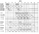
図11に図10のブロック図のメモリコントローラからメモリアレイへのデータ転送の動作タイミングチャートを示す。図8と同様に、メモリコントローラはCK0のタイミングでデータバスC0とC1に対して同じタイミングで書き込み動作を行っている。データバスB上のデータ信号はデータバスC上のデータ信号に対し、データ幅が半分で4倍のデータレートであるため、1/4クロックサイクルピッチでデータ転送を行う。メモリコントローラはCK0のタイミングでメモリサブコントローラに対し、クロックサイクルの1/4部分でデータバスC0の上位バイトデータ信号、クロックサイクルの2/4部分でデータバスC0の下位バイトデータ信号、クロックサイクルの3/4部分でデータバスC1の上位バイトデータ信号、クロックサイクルの4/4部分でデータバスC1の下位バイトデータ信号を送信する。またデータ信号と同期してデータバスC0のデータ処理用のソースクロック信号(506と507)、データバスC1のデータ処理用のソースクロック信号(508と509)を送信する。アドレス信号および制御コマンド信号の転送方式は図8と同様である。
As shown in FIG. 10, when the number of data buses C connected to the memory sub-controller is two, the address signal and control command signal from the memory controller can be transmitted simultaneously even if the data rate is quadrupled. Since there are only two buses C0 and C1, the data rate is doubled and transferred. There are four source clock signals T18, T38, T58, and T78 for source synchronous transfer related to data signals, which are 1/8 phase, 3/8 phase, 5/8 phase, and 7/8 phase delayed from the system clock T0, respectively. FIG. 11 shows an operation timing chart of data transfer from the memory controller to the memory array in the block diagram of FIG. As in FIG. 8, the memory controller performs the write operation at the same timing on the data buses C0 and C1 at the timing of CK0. Since the data signal on the data bus B has a data width which is half that of the data signal on the data bus C and is four times the data rate, data transfer is performed at a quarter clock cycle pitch. The memory controller sends to the memory sub-controller at the timing of CK0 the upper byte data signal of the data bus C0 in a quarter part of the clock cycle, the lower byte data signal of the data bus C0 in the quarter part of the clock cycle, The upper byte data signal of the data bus C1 is transmitted in the 3/4 portion, and the lower byte data signal of the data bus C1 is transmitted in the 4/4 portion of the clock cycle. Further, in synchronization with the data signal, the source clock signal (506 and 507) for data processing on the data bus C0 and the source clock signal (508 and 509) for data processing on the data bus C1 are transmitted. The address signal and control command signal transfer method is the same as in FIG.
メモリサブコントローラでは、受信したソースクロック信号(506、507、508、509)の立ち上がりエッジを用いてデータ信号503をラッチする。ソースクロック信号506でラッチしたデータバスC0の上位バイトデータ信号は318(C0-DUbuff)であり、ソースクロック信号507でラッチしたデータバスC0の下位バイトデータ信号は319(C0-DLbuff)であり、ソースクロック信号508でラッチしたデータバスC1の上位バイトデータ信号は320(C1-DUbuff)であり、ソースクロック信号509でラッチしたデータバスC1の下位バイトデータ信号は321(C1-DLbuff)である。メモリサブコントローラ内では、データバスB上を転送するためにメモリコントローラが上位/下位バイトに分割したデータ信号を一つにまとめ、システムクロック(T0)でラッチし、転送するすべての信号の位相を合わせてから、データバスC0およびC1へ送信する。データバスC0およびC1の動作は図8と同様である。
The memory sub-controller latches the data signal 503 using the rising edge of the received source clock signal (506, 507, 508, 509). The upper byte data signal of the data bus C0 latched by the source clock signal 506 is 318 (C0-DUbuff), the lower byte data signal of the data bus C0 latched by the
以上のように、1/2のデータ幅と4倍のデータレートをもつデータバスBのデータ信号に対し、ソースクロック信号を4本とエッジトリガタイプフリップフロップを4面用意することで、この4面のエッジトリガタイプフリップフロップがデータレート変換回路およびバス幅変換回路として機能し、データバスCへ送信する際にはデータレートはデータバスBの1/4倍、データ幅は2倍となり、データバスCのデータレートとデータ幅に等しくなる。 As described above, four data source clock signals and four edge trigger type flip-flops are prepared for the data signal of the data bus B having a data width of 1/2 and a data rate of 4 times. The edge trigger type flip-flop on the surface functions as a data rate conversion circuit and a bus width conversion circuit. When data is transmitted to the data bus C, the data rate is 1/4 times that of the data bus B and the data width is doubled. It becomes equal to the data rate and data width of the bus C.
図10のブロック図のメモリアレイ側からメモリコントローラ側へのデータ転送の動作タイミングチャートを図12に示す。メモリアレイ側の動作タイミングは上記方法と同じである。4倍のデータレートを実現するために4:1のセレクタ(316)を使用する。4:1のセレクタ(316)のセレクト信号(317)にはシステムクロックT0およびシステムクロックから1/4相遅れたT14を使用する。4:1セレクタの4つの入力には、システムクロック(T0)でラッチしてセレクト信号と位相を合わせたデータバスC0およびC1のデータ信号(313と315)を、上位バイトと下位バイトに分割して入力する。2本のセレクト信号(T0とT14)の値により4通りの状態が存在し、TOが"H"かつT14が"L"のとき、すなわちクロックサイクルの1/4部分でデータバスC0の上位バイトデータをデータバスBへ送信し、T0が"H"かつT14が"H"のとき、つまりクロックサイクルの2/4部分でデータバスC0の下位バイトデータをデータバスBへ送信し、T0が"L"かつT142が"H"のとき、すなわちクロックサイクルの3/4部分でデータバスC1の上位バイトデータをデータバスBへ送信し、T0が"L"かつT14が"L"のとき、すなわちクロックサイクルの4/4部分でデータバスC1の下位バイトデータをデータバスBへ送信する。データバスBへ送信するデータ信号と同期してソースクロック信号(510〜513)を送信する。 FIG. 12 shows an operation timing chart of data transfer from the memory array side to the memory controller side in the block diagram of FIG. The operation timing on the memory array side is the same as the above method. A 4: 1 selector (316) is used to achieve a quadruple data rate. For the select signal (317) of the 4: 1 selector (316), the system clock T0 and T14 delayed by 1/4 phase from the system clock are used. At the four inputs of the 4: 1 selector, the data signals (313 and 315) of the data buses C0 and C1, which are latched by the system clock (T0) and are in phase with the select signal, are divided into upper and lower bytes. Enter. There are four states depending on the values of the two select signals (T0 and T14), and when TO is "H" and T14 is "L", that is, the upper byte of the data bus C0 in the ¼ portion of the clock cycle. Data is transmitted to the data bus B, and when T0 is "H" and T14 is "H", that is, the lower byte data of the data bus C0 is transmitted to the data bus B in the 2/4 portion of the clock cycle. When L "and T142 are" H ", that is, the upper byte data of the data bus C1 is transmitted to the data bus B in 3/4 part of the clock cycle, when T0 is" L "and T14 is" L ", The lower byte data of the data bus C1 is transmitted to the data bus B in the 4/4 portion of the clock cycle. Source clock signals (510 to 513) are transmitted in synchronization with the data signal transmitted to the data bus B.
以上のように、データバスCからデータバスBの途中に4:1セレクタを挿入し、セレクト信号と位相を合わせデータ幅を1/2にした4つの入力データをセレクト信号により切り替えることで、データバスBにおいてデータレートをデータバスCの4倍に、かつデータ幅をデータバスCの1/2にすることができる。 As described above, a 4: 1 selector is inserted in the middle of the data bus C to the data bus B, and the four input data whose phase is matched with the select signal and the data width is halved are switched by the select signal. In the bus B, the data rate can be four times that of the data bus C and the data width can be ½ that of the data bus C.
以上の説明では、データバスBのデータ幅を1/2にする際の分割方法に上位/下位バイトを使用したが、その他にも偶数/奇数バイトで分割する等方法は多数ある。また、その分割した分割単位の転送順番も任意である。 In the above description, the upper / lower bytes are used as the dividing method when the data width of the data bus B is halved, but there are many other methods such as dividing even / odd bytes. Also, the transfer order of the divided units is arbitrary.
メモリサブコントローラにデータバスBが1本、データバスCが2本接続している場合、データバスBのデータ幅を半分にしてデータレートを4倍にすることで、データバスBのバンド幅とデータバスCのバンド幅の総和は等しくなる。 When one data bus B and two data buses C are connected to the memory sub-controller, the data bus B bandwidth is reduced by halving the data width of the data bus B and quadrupling the data rate. The sum of the bandwidths of the data bus C is equal.
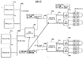
本発明の他の実施例を図13に示す。図1との相違点は、データバスBのデータ幅を1/2、データレートを4倍にしていて、1つのメモリサブコントローラに接続しているデータバスBのバンド幅を該メモリサブコントローラに接続しているデータバスCのバンド幅の総和に等しくしている点である。構成要素・動作タイミングは本発明の「データ幅を1/2にしてデータレートを4倍にする方法」で述べている。データバスBのデータ幅が半分になるために、メモリコントローラおよびメモリサブコントローラで必要なピン数が削減され、図1のLSIパッケージよりも小さいLSIパッケージが使用可能となり、コストを削減できる。 Another embodiment of the present invention is shown in FIG. The difference from FIG. 1 is that the data width of the data bus B is halved and the data rate is quadrupled, and the bandwidth of the data bus B connected to one memory sub-controller is set in the memory sub-controller. In other words, the sum of the bandwidths of the connected data bus C is made equal. The components and the operation timing are described in the “method of doubling the data rate by halving the data width” of the present invention. Since the data width of the data bus B is halved, the number of pins required for the memory controller and the memory sub-controller is reduced, and an LSI package smaller than the LSI package of FIG. 1 can be used, thereby reducing costs.
本発明の他の実施例を図14に示す。図1との相違点は、データバスBのデータ幅を1/2、データレートが4倍にしていて、1つのメモリサブコントローラに接続しているデータバスBのバンド幅を該メモリサブコントローラに接続しているデータバスCのバンド幅の総和に等しくしている点である。図13との相違点は、メモリコントローラのピン数削減は行わずにメモリコントローラに接続するデータバスCの本数を2倍にしていることである。構成要素・動作タイミングは本発明の「データ幅を1/2にしてデータレートを4倍にする方法」で述べている。データバスBのデータ幅が半分になるために、メモリコントローラに接続できるデータバスBの本数が倍増し、データバスBでデータバスCの総和のバンド幅を確保しながらメモリの容量を倍にすることが可能となる。 Another embodiment of the present invention is shown in FIG. The difference from FIG. 1 is that the data width of the data bus B is ½, the data rate is quadrupled, and the bandwidth of the data bus B connected to one memory sub-controller is set to the memory sub-controller. In other words, the sum of the bandwidths of the connected data bus C is made equal. The difference from FIG. 13 is that the number of data buses C connected to the memory controller is doubled without reducing the number of pins of the memory controller. The components and the operation timing are described in the “method of doubling the data rate by halving the data width” of the present invention. Since the data width of the data bus B is halved, the number of data buses B that can be connected to the memory controller is doubled, and the data bus B doubles the memory capacity while ensuring the total bandwidth of the data bus C. It becomes possible.
本発明の他の実施例を図15に示す。図1との相違点はデータバスBのデータ幅を1/2にして、データレートを2倍にしていることである。前述の実施例はいずれもメモリサブコントローラにおいてメモリアレイに接続したデータバスCの本数分のバンド幅をデータバスBで確保するものであった。しかし、データバスBのデータ幅を半分にし、データレートを倍にして、データバスAとデータバスBのバンド幅の釣り合いを取ったシステム構成にすることも可能である。この場合、データバスBのバンド幅は変化していないが、データバスBのデータ幅が半分になるので、メモリコントローラおよびメモリサブコントローラで必要なピン数が削減可能である。つまりメモリコントローラおよびメモリサブコントローラのLSIパッケージにかかるコストを削減できる。メモリサブコントローラのブロック図、タイミングチャート等はデータバスの幅が異なるだけで図7のブロック図、図8および図9のタイミングチャートと同一である。 Another embodiment of the present invention is shown in FIG. The difference from FIG. 1 is that the data width of the data bus B is halved and the data rate is doubled. In all of the above-described embodiments, the data bus B secures the bandwidth corresponding to the number of data buses C connected to the memory array in the memory sub-controller. However, it is also possible to halve the data width of the data bus B and double the data rate so as to achieve a system configuration that balances the bandwidth of the data bus A and the data bus B. In this case, the bandwidth of the data bus B is not changed, but the data width of the data bus B is halved, so that the number of pins necessary for the memory controller and the memory sub-controller can be reduced. That is, the cost for the LSI package of the memory controller and the memory sub-controller can be reduced. The block diagram and timing chart of the memory sub-controller are the same as the block diagrams of FIG. 7, FIG. 8 and FIG. 9 except that the width of the data bus is different.
本発明の他の実施例を図16〜図20を用いて説明する。図16はメモリサブコントローラのブロック図である。302〜303、810〜812および820〜822はメモリサブコントローラ(103)を構成する要素および信号線である。800〜803はメモリコントローラとのインターフェイス信号であり、この信号線を用いてメモリアレイに対する制御信号を受信しデータ信号を送受信する。804〜807はデータバスCのインターフェイス信号であり、この信号線を用いてメモリアレイに対する制御信号を送信しデータ信号を送受信する。
Another embodiment of the present invention will be described with reference to FIGS. FIG. 16 is a block diagram of the memory sub-controller.
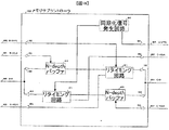
図16のメモリサブコントローラは、入力バッファ(302)、出力バッファ(303)、N-depthバッファ(810)、リタイミング回路(811)、同期化信号発生回路(812)から構成される。 The memory sub-controller in FIG. 16 includes an input buffer (302), an output buffer (303), an N-depth buffer (810), a retiming circuit (811), and a synchronization signal generation circuit (812).
メモリコントローラとのインターフェイスは、メモリコントローラ−メモリサブコントローラ間で送受信するデータ信号(802)と受信データに対するソースクロック信号(801)、送信データに対するソースクロック信号(803)、メモリコントローラからの同期化信号(800)から構成される。メモリコントローラから送信されるアドレス信号および制御信号はデータ信号(802)の一部として考える。メモリアレイとのインターフェイスは、メモリサブコントローラ−メモリアレイ間で送受信するデータ信号(806)と送信データに対するソースクロック信号(805)、受信データに対するソースクロック信号(807)、メモリアレイへの同期化信号(804)から構成される。メモリアレイへ送信するアドレス信号および制御信号はデータ信号の一部として考える。 The interface with the memory controller consists of a data signal (802) transmitted and received between the memory controller and the memory sub-controller, a source clock signal (801) for received data, a source clock signal (803) for transmitted data, and a synchronization signal from the memory controller. (800). The address signal and control signal transmitted from the memory controller are considered as part of the data signal (802). The interface with the memory array consists of the data signal (806) transmitted and received between the memory sub-controller and the memory array, the source clock signal (805) for the transmission data, the source clock signal (807) for the reception data, and the synchronization signal to the memory array (804). The address signal and control signal transmitted to the memory array are considered as part of the data signal.
メモリコントローラとメモリサブコントローラ間が2cycleソース同期転送である場合の図16に示した2-depthバッファ(N=2)のブロック図、リタイミング回路のブロック図、メモリコントローラからメモリアレイへのデータ転送の動作タイミングチャートをそれぞれ図17、図18、図19に示す。図16に示すようにソース同期転送のマスター側には同期信号発生回路を搭載する。図16〜図20ではメモリコントローラとメモリサブコントローラ間のデータ転送ではメモリコントローラをマスターとし、メモリサブコントローラとメモリアレイ間のデータ転送ではメモリサブコントローラをマスターとしている。 16 is a block diagram of the 2-depth buffer (N = 2) shown in FIG. 16, a block diagram of a retiming circuit, and data transfer from the memory controller to the memory array when the memory controller and the memory sub-controller are in 2-cycle source synchronous transfer. The operation timing charts are shown in FIGS. 17, 18 and 19, respectively. As shown in FIG. 16, a synchronization signal generating circuit is mounted on the master side of the source synchronous transfer. 16 to 20, the memory controller is the master for data transfer between the memory controller and the memory sub-controller, and the memory sub-controller is the master for data transfer between the memory sub-controller and the memory array.
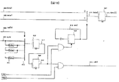
図17の2-depthバッファは2個のエッジトリガタイプフリップフロップ(907)と1個のリセット条件付きエッジトリガタイプフリップフロップ(908)と数個のAND・NOTゲートから構成される。 The 2-depth buffer in FIG. 17 includes two edge trigger type flip-flops (907), one edge trigger type flip-flop (908) with a reset condition, and several AND / NOT gates.
図18のリタイミング回路は1個のエッジトリガタイプフリップフロップ(907)と3個のリセット条件付きエッジトリガタイプフリップフロップ(908)と複数のディレイゲート(911)および、各ディレイゲート通過信号を選択するM:1のセレクタ(912)と数個のAND・NOTゲートから構成される。同期化信号(910)が必ず2cycle転送で行われるようにディレイゲート(911)とセレクト信号(909)を用いて調節できるようにする。 The retiming circuit of FIG. 18 selects one edge trigger type flip-flop (907), three edge trigger type flip-flops (908) with reset conditions, a plurality of delay gates (911), and each delay gate passing signal. It consists of M: 1 selector (912) and several AND / NOT gates. The delay signal (911) and the select signal (909) can be adjusted so that the synchronization signal (910) is surely performed in two cycles.
次に、図19を用いてメモリコントローラからメモリサブコントローラへの2cycleソース同期転送時の2-depthバッファとリタイミング回路の動作を説明する。まず、送信側(メモリコントローラ)からCK0のサイクルで同期化信号がアサートされる。図16ではこの信号は同期化信号発生回路(812)が出力しているが、メモリコントローラのリセット信号及びリセット信号をクロック信号でラッチしたものを使用してもよい。同期化信号はメモリコントローラ内部と外部に転送され、内部では同期化信号をもとにして同期化信号がアサートされた2cycle後にメモリサブコントローラへのソースクロック信号(801,902)を出力する。ソースクロック信号は送信するデータウィンドウの中央にクロックエッジがくるように、システムクロックT0の逆相であるT24を用いる。直接外部へ出力された同期化信号はメモリサブコントローラに入力する(800,910)。この時の転送サイクルが必ず2cycleになるように受信側(メモリサブコントローラ)で調節する。メモリサブコントローラでは入力した同期化信号のアサートがトリガとなりメモリコントローラへのソースクロック信号(803,916)が出力され、同時にリタイミング時のセレクト信号(913)が動作する。CK3のサイクルにはメモリコントローラが出力したソースクロック信号がメモリサブコントローラへ到着し、ソースクロック信号(902)がトリガとなり2-depthバッファのセレクト信号(903)および2-depthバッファへのトリガクロック信号(903,904)が動作する。受信データ(901)を2-depthバッファに交互に取り込むために、ソースクロック信号(902)をセレクト信号(903)でマスクする。 Next, operations of the 2-depth buffer and the retiming circuit at the time of two-cycle source synchronous transfer from the memory controller to the memory sub-controller will be described with reference to FIG. First, the synchronization signal is asserted in the cycle CK0 from the transmission side (memory controller). In FIG. 16, this signal is output from the synchronization signal generation circuit (812). However, a reset signal of the memory controller and a signal obtained by latching the reset signal with a clock signal may be used. The synchronization signal is transferred to the inside and outside of the memory controller, and internally, the source clock signal (801, 902) is output to the memory sub-controller after 2 cycles when the synchronization signal is asserted based on the synchronization signal. The source clock signal uses T24 which is the opposite phase of the system clock T0 so that the clock edge comes to the center of the data window to be transmitted. The synchronization signal directly output to the outside is input to the memory sub-controller (800, 910). The receiving side (memory sub-controller) adjusts so that the transfer cycle is always 2 cycles. In the memory sub-controller, the assertion of the input synchronization signal is triggered to output the source clock signal (803, 916) to the memory controller, and at the same time, the select signal (913) at the time of retiming operates. In the CK3 cycle, the source clock signal output from the memory controller arrives at the memory sub-controller, and the source clock signal (902) is the trigger and the 2-depth buffer select signal (903) and the trigger clock signal to the 2-depth buffer (903,904) operates. In order to alternately take received data (901) into the 2-depth buffer, the source clock signal (902) is masked with the select signal (903).
メモリコントローラがCK11のタイミングで4つの連続したデータ信号を送信した場合、メモリコントローラが出力したデータ信号は前述の同期化信号とほぼ同じタイミングでメモリサブコントローラに入力する(901)。ここでは伝播遅延時間が1cycle以上の場合を示し、1cycle以下の場合は後述する。メモリサブコントローラ内部ではすでに動作している2-depthバッファのセレクト信号がマスクとなり、ソースクロック信号をセレクト信号でマスクしたトリガクロック信号(903,904)を用いて、入力データ(901)を2-depthバッファへ交互に取り込む。2-depthバッファに取り込まれたデータ(905,906)は図19のタイミングチャートに示すように、セレクト信号(913)が"H"のときデータ信号(906)が選択され、セレクト信号(913)が"L"のときデータ信号(905)が選択される。セレクト信号で選択されたデータ信号(914)は次のメモリアレイ側のソース同期転送の出力タイミングに同期させるためにシステムクロックT0でラッチする。ラッチしたデータ信号(915)はそのソースクロック信号とともにメモリアレイへ送出される。 When the memory controller transmits four consecutive data signals at the timing of CK11, the data signal output from the memory controller is input to the memory sub-controller at almost the same timing as the above-mentioned synchronization signal (901). Here, a case where the propagation delay time is 1 cycle or more is shown, and a case where the propagation delay time is 1 cycle or less will be described later. Inside the memory sub-controller, the select signal of the 2-depth buffer that is already operating becomes a mask, and the input data (901) is converted to the 2-depth buffer using the trigger clock signal (903,904) that masks the source clock signal with the select signal. Alternately. As shown in the timing chart of FIG. 19, the data (905, 906) taken into the 2-depth buffer is selected when the select signal (913) is “H”, and the select signal (913) is “ When L ", the data signal (905) is selected. The data signal (914) selected by the select signal is latched by the system clock T0 in order to synchronize with the output timing of the next source synchronous transfer on the memory array side. The latched data signal (915) is sent to the memory array together with its source clock signal.
以上はメモリコントローラからメモリアレイへのデータ転送であるが、その逆のメモリアレイからメモリコントローラへのデータ転送も同様である。また、図17でソースクロック信号(902)と2-depthバッファセレクト信号(903)のANDをとっているが、907のフリップフロップをクロック条件付きエッジトリガフリップフロップを使用し、ソースクロック信号(902)をフリップフロップのクロック端子へ直接、2-depthバッファセレクト信号(903)をフリップフロップのクロック条件端子へ直接またはNOTゲートを介して接続し、実現することも可能である。 The above is data transfer from the memory controller to the memory array, but the reverse is also true for data transfer from the memory array to the memory controller. In FIG. 17, the AND of the source clock signal (902) and the 2-depth buffer select signal (903) is taken, and the 907 flip-flop is used as a clock conditional edge trigger flip-flop, and the source clock signal (902 ) Can be directly connected to the clock terminal of the flip-flop, and the 2-depth buffer select signal (903) can be directly connected to the clock condition terminal of the flip-flop or via a NOT gate.
メモリコントローラとメモリサブコントローラ間の信号の伝播遅延時間が1cycle以内であるタイミングチャートを図20に示す。基本的な動作は図19の伝播遅延時間が1cycle以上の場合と差異はない。ただし、同期化信号は必ず2cycle転送になるようにディレイゲート(911)を用いて調節する。図19との違いは、CK2のタイミングでメモリコントローラが送信したソースクロック信号はそのクロックサイクル内でメモリサブコントローラに到達することである。また、CK11のタイミングでメモリコントローラが送信したデータ信号はソースクロック信号と同じタイミングでメモリサブコントローラに到達することである。2-depthバッファのトリガクロック信号(903,904)はソースクロック信号(902)をマスクしただけのものであるから、データ信号(901)とソースクロック信号(902)の相対的な時間関係は変化せずに図19同様に2-depthバッファへ交互に取り込まれる。2-depthバッファのトリガクロック信号(903,904)はソースクロック信号(902)に対し周期が2倍であるため、2-depthバッファのウィンドウ幅は2cycle分存在し、伝播遅延時間が1cycle以内である場合でも次のサイクルまでデータ信号を保持できる。2-depthバッファに取り込まれたデータ信号(905,906)は、図19の伝播遅延時間が1cycle以上である場合と同じタイミングのセレクト信号(913)を用いるので、データ転送サイクルは2cycleとかわりない。 FIG. 20 shows a timing chart in which the propagation delay time of signals between the memory controller and the memory sub-controller is within 1 cycle. The basic operation is not different from the case where the propagation delay time in FIG. 19 is 1 cycle or more. However, the synchronization signal is adjusted using the delay gate (911) so that it is always 2 cycle transfer. The difference from FIG. 19 is that the source clock signal transmitted by the memory controller at the timing of CK2 reaches the memory sub-controller within the clock cycle. The data signal transmitted from the memory controller at the timing of CK11 arrives at the memory sub-controller at the same timing as the source clock signal. Since the trigger clock signal (903,904) of the 2-depth buffer is only a mask of the source clock signal (902), the relative time relationship between the data signal (901) and the source clock signal (902) does not change. As in FIG. 19, they are alternately taken into the 2-depth buffer. The trigger clock signal (903,904) of the 2-depth buffer has a period twice that of the source clock signal (902), so the window width of the 2-depth buffer exists for 2 cycles and the propagation delay time is within 1 cycle. However, the data signal can be held until the next cycle. Since the data signal (905, 906) taken into the 2-depth buffer uses the select signal (913) having the same timing as that in the case where the propagation delay time in FIG. 19 is 1 cycle or more, the data transfer cycle does not change to 2 cycles.
上記実施例では2cycleのソース同期転送について説明したが、3cycle以上のソース同期転送についても同様に実現可能である。また、図1〜図15で説明した実施例についても本実施例を採用し、マルチサイクルのソース同期転送を実現することも可能である。 In the above embodiment, the source synchronous transfer of 2 cycles has been described, but the source synchronous transfer of 3 cycles or more can be similarly realized. Also, the present embodiment can be adopted for the embodiments described with reference to FIGS. 1 to 15 to realize multi-cycle source synchronous transfer.
上記実施例では、エッジトリガタイプフリップフロップのトリガクロック信号に、クロック信号の立ち上がりエッジを用いているが、立ち下がりエッジまたは立ち上がりと立ち下がりの両エッジを用いても構成可能である。 In the above embodiment, the rising edge of the clock signal is used as the trigger clock signal of the edge trigger type flip-flop. However, the falling edge or both rising and falling edges can be used.
また、ソース同期転送用にT14、T24、T34、T18、T38、T58、T78というタイミングのクロック信号を使用しているが、このクロック信号タイミングに関しても送信するデータのウィンドウを捕らえられるものであれば他のタイミングを用いてもよい。 In addition, clock signals with timings of T14, T24, T34, T18, T38, T58, and T78 are used for source synchronous transfer, but if this clock signal timing can also capture the window of data to be transmitted, Other timings may be used.
また、上記実施例ではメモリアクセス手順にSDRAMに対する手順と同様なものを示したが、これは同期式RAMに適用した例であり、メモリアレイをSDRAMおよびSDRAMを用いたメモリモジュールに限定するものではない。 In the above embodiment, the same memory access procedure as that for the SDRAM is shown, but this is an example applied to the synchronous RAM, and the memory array is not limited to the memory module using SDRAM and SDRAM. Absent.
また、上記実施例では、メモリサブコントローラに接続されているデータバスCの本数は2本であるが、これは一つの例であり、メモリコントローラに接続されているデータバスCの本数は1本または2本以上であってもよい。 In the above embodiment, the number of data buses C connected to the memory sub-controller is two. However, this is one example, and the number of data buses C connected to the memory controller is one. Or two or more may be sufficient.
上記すべての実施例において、プロセッサとメモリアレイに関して述べていて、I/Oバスに関しては触れていない。しかし、データバスに関してはメモリコントローラを挟んで、メモリアレイ側とそれ以外の2つに分類できるため、I/Oバスはプロセッサ側に含めて考える。 In all the above embodiments, the processor and the memory array are described, but the I / O bus is not mentioned. However, since the data bus can be classified into the memory array side and the other two with the memory controller in between, the I / O bus is considered to be included in the processor side.
101、201・・プロセッサ
102、202・・メモリコントローラ
103・・メモリサブコントローラ
104、204・・メモリアレイ
105、205・・データバスA
106、206・・データバスB
107、207・・データバスC
101, 201 ・ Processor
102, 202 ・ ・ Memory controller
103 ・ ・ Memory sub-controller
104, 204 ... Memory array
105, 205 ・ ・ Data bus A
106,206 ・ ・ Data bus B
107, 207 ・ ・ Data bus C
Claims (3)
当該計算機システムは、メモリコントローラとメモリアレイ間に複数のデータ転送路接続手段を設け、前記メモリコントローラとそれぞれの前記データ転送路接続手段の間をデータ転送路接続手段ごとに第一のデータ転送路で接続し、さらに、前記データ転送路接続手段ごとに前記データ転送路接続手段と前記メモリアレイ間をメモリアレイごとに第二のデータ転送路で接続して、前記メモリコントローラと前記メモリアレイの間で相互にデータ転送をおこなうように構成し、
前記プロセッサが複数の第三のデータ転送路により前記メモリコントローラに接続されるとともに、複数の前記データ転送路接続手段が前記メモリコントローラに接続され、
前記第一のデータ転送路及び第二のデータ転送路は、転送するデータと共に前記第一のデータ転送路及と第二のデータ転送路とで異なるデータ転送のクロック情報を有してソース同期転送され、
前記第一のデータ転送路は前記第二のデータ転送路に比べ、データ転送路幅が小さくかつ転送周波数が大きくし、
前記第一のデータ転送路のデータ転送バンド幅は、前記第二のデータ転送路のデータ転送バンド幅の総和に等しいことを特徴とする計算機システム。 In a computer system comprising a plurality of processors, a memory controller, and a plurality of memory arrays,
The computer system is provided with a plurality of data transfer paths connecting means between the memory controller and memory array, the first data transfer channel for each data transfer channel connecting means between the memory controller and each of said data transfer path connecting means in connecting, further, the between the data transfer path connecting means said memory array connected by the second data transfer channel for each memory array for each of the data transfer path connecting means, between said memory array and the memory controller Configured to transfer data to each other,
The processor is connected to the memory controller by a plurality of third data transfer paths, and a plurality of the data transfer path connection means are connected to the memory controller,
The first data transfer path and the second data transfer path have the data to be transferred and the clock information of the data transfer different between the first data transfer path and the second data transfer path, and the source synchronous transfer And
The first data transfer path has a smaller data transfer path width and a higher transfer frequency than the second data transfer path,
The computer system according to claim 1, wherein a data transfer bandwidth of the first data transfer path is equal to a sum of data transfer bandwidths of the second data transfer path.
前記第一のデータ転送路と第二のデータ転送路でデータを相互に転送することを特徴とする請求項1に記載の計算機システム。 The computer system according to claim 1, wherein data is transferred between the first data transfer path and the second data transfer path.
当該計算機システムは、メモリコントローラとメモリアレイの間に複数のデータ転送路接続手段を設け、 The computer system includes a plurality of data transfer path connection means between the memory controller and the memory array,
前記メモリコントローラと前記データ転送路接続手段の間をデータ転送路接続手段ごとに第一のデータ転送路で接続し、さらに、前記データ転送路接続手段ごとに前記データ転送路接続手段と前記複数のメモリアレイ間をメモリアレイごとに第二のデータ転送路で接続して、前記メモリコントローラと前記メモリアレイの間で相互にソース同期データ転送をおこなうように構成し、 A first data transfer path is connected between the memory controller and the data transfer path connection means for each data transfer path connection means, and further, the data transfer path connection means and the plurality of data transfer paths are connected for each data transfer path connection means. The memory arrays are connected to each other by a second data transfer path for each memory array, and configured to perform source synchronous data transfer between the memory controller and the memory array,
前記メモリコントローラと前記プロセッサは第三のデータ転送路で接続するように構成され、 The memory controller and the processor are configured to be connected by a third data transfer path,
前記第一のデータ転送路のデータ転送バンド幅は、前記第三のデータ転送路のデータ転送バンド幅に等しく、かつ、The data transfer bandwidth of the first data transfer path is equal to the data transfer bandwidth of the third data transfer path, and
前記第一のデータ転送路のデータ転送路幅は、前記第二のデータ転送路のデータ転送路幅より小さいことを特徴とする計算機システム。 The computer system according to claim 1, wherein a data transfer path width of the first data transfer path is smaller than a data transfer path width of the second data transfer path.
Priority Applications (1)
| Application Number | Priority Date | Filing Date | Title |
|---|---|---|---|
| JP2004167936A JP4305286B2 (en) | 2004-06-07 | 2004-06-07 | Computer system |
Applications Claiming Priority (1)
| Application Number | Priority Date | Filing Date | Title |
|---|---|---|---|
| JP2004167936A JP4305286B2 (en) | 2004-06-07 | 2004-06-07 | Computer system |
Related Parent Applications (1)
| Application Number | Title | Priority Date | Filing Date |
|---|---|---|---|
| JP22010698A Division JP3644265B2 (en) | 1998-08-04 | 1998-08-04 | Memory subsystem |
Publications (3)
| Publication Number | Publication Date |
|---|---|
| JP2004295915A JP2004295915A (en) | 2004-10-21 |
| JP2004295915A5 JP2004295915A5 (en) | 2005-09-29 |
| JP4305286B2 true JP4305286B2 (en) | 2009-07-29 |
Family
ID=33411328
Family Applications (1)
| Application Number | Title | Priority Date | Filing Date |
|---|---|---|---|
| JP2004167936A Expired - Fee Related JP4305286B2 (en) | 2004-06-07 | 2004-06-07 | Computer system |
Country Status (1)
| Country | Link |
|---|---|
| JP (1) | JP4305286B2 (en) |
Families Citing this family (1)
| Publication number | Priority date | Publication date | Assignee | Title |
|---|---|---|---|---|
| JP2012194819A (en) * | 2011-03-17 | 2012-10-11 | Mitsubishi Electric Corp | Program switching circuit and electronic apparatus |
-
2004
- 2004-06-07 JP JP2004167936A patent/JP4305286B2/en not_active Expired - Fee Related
Also Published As
| Publication number | Publication date |
|---|---|
| JP2004295915A (en) | 2004-10-21 |
Similar Documents
| Publication | Publication Date | Title |
|---|---|---|
| US7808844B2 (en) | Methods and apparatus for improved memory access | |
| KR100382736B1 (en) | Semiconductor memory device having different data rates in read operation and write operation | |
| US8700818B2 (en) | Packet based ID generation for serially interconnected devices | |
| JP4812976B2 (en) | Register, memory module and memory system | |
| JP4070051B2 (en) | Data masking method and circuit for semiconductor memory device, and semiconductor memory device having the circuit | |
| KR100396944B1 (en) | Semiconductor memory device and memory system using the same | |
| US7245147B1 (en) | Interface for a programmable logic device | |
| US6806733B1 (en) | Multiple data rate interface architecture | |
| US7668022B2 (en) | Integrated circuit for clock generation for memory devices | |
| JP5232019B2 (en) | Apparatus, system, and method for multiple processor cores | |
| US7965568B2 (en) | Semiconductor integrated circuit device and method of testing same | |
| US20050278490A1 (en) | Memory access control apparatus and method of controlling memory access | |
| US7504855B1 (en) | Multiple data rate memory interface architecture | |
| KR20060111465A (en) | Integrated circuit with bi-modal data strobe | |
| KR20050061123A (en) | Data control circuit in the double data rate synchronous dram controller | |
| JP3644265B2 (en) | Memory subsystem | |
| KR100719146B1 (en) | Multi port memory device with serial input/output interface | |
| JP4305286B2 (en) | Computer system | |
| US20050248367A1 (en) | Digital bus synchronizer for generating read reset signal | |
| JP4952177B2 (en) | Storage device | |
| KR0164805B1 (en) | Inner column address generating circuit for a burst mode | |
| JPH10340222A (en) | Input circuit and output circuit of memory device | |
| US7269681B1 (en) | Arrangement for receiving and transmitting PCI-X data according to selected data modes | |
| WO2021012767A1 (en) | Bus for interconnection between memory controller and memory devices | |
| JP2008217379A (en) | Serial transfer method |
Legal Events
| Date | Code | Title | Description |
|---|---|---|---|
| A521 | Written amendment |
Free format text: JAPANESE INTERMEDIATE CODE: A523 Effective date: 20050729 |
|
| A621 | Written request for application examination |
Free format text: JAPANESE INTERMEDIATE CODE: A621 Effective date: 20050729 |
|
| RD01 | Notification of change of attorney |
Free format text: JAPANESE INTERMEDIATE CODE: A7421 Effective date: 20060421 |
|
| A131 | Notification of reasons for refusal |
Free format text: JAPANESE INTERMEDIATE CODE: A131 Effective date: 20080513 |
|
| A521 | Written amendment |
Free format text: JAPANESE INTERMEDIATE CODE: A523 Effective date: 20080711 |
|
| A131 | Notification of reasons for refusal |
Free format text: JAPANESE INTERMEDIATE CODE: A131 Effective date: 20080909 |
|
| A521 | Written amendment |
Free format text: JAPANESE INTERMEDIATE CODE: A523 Effective date: 20081105 |
|
| A131 | Notification of reasons for refusal |
Free format text: JAPANESE INTERMEDIATE CODE: A131 Effective date: 20090120 |
|
| A521 | Written amendment |
Free format text: JAPANESE INTERMEDIATE CODE: A523 Effective date: 20090323 |
|
| TRDD | Decision of grant or rejection written | ||
| A01 | Written decision to grant a patent or to grant a registration (utility model) |
Free format text: JAPANESE INTERMEDIATE CODE: A01 Effective date: 20090407 |
|
| A01 | Written decision to grant a patent or to grant a registration (utility model) |
Free format text: JAPANESE INTERMEDIATE CODE: A01 |
|
| A61 | First payment of annual fees (during grant procedure) |
Free format text: JAPANESE INTERMEDIATE CODE: A61 Effective date: 20090420 |
|
| FPAY | Renewal fee payment (event date is renewal date of database) |
Free format text: PAYMENT UNTIL: 20120515 Year of fee payment: 3 |
|
| FPAY | Renewal fee payment (event date is renewal date of database) |
Free format text: PAYMENT UNTIL: 20120515 Year of fee payment: 3 |
|
| FPAY | Renewal fee payment (event date is renewal date of database) |
Free format text: PAYMENT UNTIL: 20130515 Year of fee payment: 4 |
|
| LAPS | Cancellation because of no payment of annual fees |