JP4278317B2 - Arithmetic device and receiving device - Google Patents
Arithmetic device and receiving device Download PDFInfo
- Publication number
- JP4278317B2 JP4278317B2 JP2001204162A JP2001204162A JP4278317B2 JP 4278317 B2 JP4278317 B2 JP 4278317B2 JP 2001204162 A JP2001204162 A JP 2001204162A JP 2001204162 A JP2001204162 A JP 2001204162A JP 4278317 B2 JP4278317 B2 JP 4278317B2
- Authority
- JP
- Japan
- Prior art keywords
- data
- unit
- data group
- input
- address
- Prior art date
- Legal status (The legal status is an assumption and is not a legal conclusion. Google has not performed a legal analysis and makes no representation as to the accuracy of the status listed.)
- Expired - Fee Related
Links
Images
Classifications
-
- G—PHYSICS
- G06—COMPUTING OR CALCULATING; COUNTING
- G06F—ELECTRIC DIGITAL DATA PROCESSING
- G06F9/00—Arrangements for program control, e.g. control units
- G06F9/06—Arrangements for program control, e.g. control units using stored programs, i.e. using an internal store of processing equipment to receive or retain programs
- G06F9/30—Arrangements for executing machine instructions, e.g. instruction decode
- G06F9/30003—Arrangements for executing specific machine instructions
- G06F9/30007—Arrangements for executing specific machine instructions to perform operations on data operands
- G06F9/3001—Arithmetic instructions
Landscapes
- Engineering & Computer Science (AREA)
- Theoretical Computer Science (AREA)
- Software Systems (AREA)
- Physics & Mathematics (AREA)
- General Physics & Mathematics (AREA)
- General Engineering & Computer Science (AREA)
- Computational Mathematics (AREA)
- Pure & Applied Mathematics (AREA)
- Mathematical Optimization (AREA)
- Mathematical Analysis (AREA)
- Complex Calculations (AREA)
- Executing Machine-Instructions (AREA)
- Communication Control (AREA)
- Compression, Expansion, Code Conversion, And Decoders (AREA)
- Image Processing (AREA)
Description
【0001】
【発明の属する技術分野】
本発明は演算装置および受信装置に関し、特に、複数のデータから構成されるデータ群を入力し、先に入力された他のデータ群との間で所定の演算処理を実行する演算装置および受信装置に関する。
【0002】
【従来の技術】
情報処理の分野では、複数のデータから構成されるデータ群を入力し、先に入力された他のデータ群との間で所定の演算処理を行う場合がある。
【0003】
このような演算は、例えば、W−CDMA(Wideband Code Division Multiple Access)方式の携帯電話システムにおいて、基地局との相関値を算出する場合に、受信信号を1スロット単位で積分する際に用いられる。
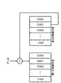
【0004】
図8は、W−CDMAに使用されている従来の積分回路の構成例を示す図である。この図に示すように、従来の積分回路は、ADD(Adder:加算回路)10、DP−RAM(Dual Port Random Access Memory)11によって構成されている。
【0005】
ここで、ADD10は、入力されたデータ(DATA)と、DP−RAM11から読み出されたデータとを加算し、演算即ち加算の結果のデータΣ1を出力する。
【0006】
DP−RAM11は、Read_B信号がアクティブである場合において、Address_B信号によって指定されたアドレスに格納されているデータをΣ2として読み出して出力する。また、Write信号がアクティブである場合において、Address_A信号によって指定される領域に対して、ADD10から出力されるデータを書き込む。
【0007】
なお、DP−RAM11は、クロック信号(CLOCK)に同期して動作する。
次に、以上の従来例の動作について説明する。
【0008】
先ず、第1番目のデータ群が入力される際には、図示せぬ制御装置からの制御信号により、DP−RAM11からの出力データが“0”になるように制御される。その結果、ADD10へ供給されるデータは“0”となり、第1番目のデータ群に対しては、“0”が加算されるため、ADD10から入力されたデータがそのまま出力されることになる。
【0009】
ADD10から出力されたデータは、Address_B信号によって指定されるアドレスへ順次格納される。ここで、Address_B信号は、“0000”から1ずつインクリメントされ、最大アドレス値に到達した場合には、“0000”に復元する。なお、この処理は各データ群のデータについて行われ、ADD10から出力された各データ群のデータは、アドレス“0000”から最大アドレスまでに対して順次格納されることになる。
【0010】
その結果、第1番目のデータ群がそのままの状態で、アドレス“0000”から最大アドレスのそれぞれに対して格納された状態となる。
続いて、第2番目のデータ群が入力されると、DP−RAM11は、アドレス“0000”から、既に格納されているデータ(第1番目のデータ群の最初のデータ)を読み出し、ADD10に供給する。
【0011】
ADD10は、第2番目のデータ群の先頭のデータと、DP−RAM11から供給された第1番目のデータ群の先頭のデータとを加算し、計算結果のデータΣ1として出力する。
【0012】
このとき、Write信号がアクティブとされており、また、Address_A信号はDP−RAM11のアドレス“0000”を指定する信号を出力していることから、計算結果のデータΣ1は、DP−RAM11の先頭アドレスに格納されることになる。
【0013】
なお、データΣ1を書き込むタイミングよりも、データΣ2を読み出すタイミングの方が、1クロック分だけ先行しているので、データΣ1によってデータΣ2が上書きされ、データΣ2が失われることはない。
【0014】
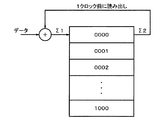
図9は、従来の演算装置の動作を簡単に説明するための図である。
この図に示すように、DP−RAM11のアドレス“0000”から1クロック前に読み出されたデータΣ2は、新たに入力されたデータと加算され、計算結果のデータΣ1として、同一のアドレス“0000”に書き込まれることになる。
【0015】
同様の動作は、次に入力されたデータと、アドレス“0001”に格納されているデータとの間でも実行され、計算結果のデータΣ1がアドレス“0001”に格納されることになる。
【0016】
以上のような動作が所定の回数繰り返されることにより、入力されたデータ群を順次加算し、得られた結果を積分値として出力することが可能になる。
【0017】
【発明が解決しようとする課題】
ところで、以上に示す従来の演算装置では、DP−RAM11を使用していたため、読み出し動作と書き込み動作を並行して行うことが可能となるので、演算処理を高速に行うことができるというメリットを有する一方で、DP−RAM11は、SP−RAM(Single Port RAM)に比較して、チップ上に占める面積が大きいため、演算装置のサイズを小型化することが困難であるという問題点があった。
【0018】
その結果、このような演算装置を搭載した携帯電話等の受信装置のサイズを小型化することが困難であるという問題点もあった。
本発明は、以上のような状況に鑑みてなされたものであり、高速動作が可能であるとともに、装置の小型化が可能である演算装置および受信装置を提供することを目的とする。
【0019】
【課題を解決するための手段】
本発明では上記課題を解決するために、図1に示す、複数のデータから構成されるデータ群を入力し、先に入力された他のデータ群との間で所定の演算処理を実行する演算装置において、前記データ群を入力する入力手段20と、前記データ群の少なくとも一部又は全部を格納することが可能な容量を有する第1乃至第n(n>1)の格納手段23−1〜23−2と、前記第1乃至第nの格納手段23−1〜23−2の何れかを選択し、既に格納されているデータ群を読み出す読み出し手段24と、前記読み出し手段24によって読み出されたデータ群と、前記入力手段20から新たに入力されたデータ群との間で所定の演算を行う演算手段21と、前記演算手段21の演算結果を、前記読み出し手段24が読み出しの対象としていない所定の格納手段に対して書き込む書き込み手段22と、を有することを特徴とする演算装置が提供される。
【0020】
ここで、入力手段20は、データ群を入力する。第1乃至第n(n>1)の格納手段23−1〜23−2は、データ群の少なくとも一部又は全部を格納することが可能な容量を有する。読み出し手段24は、第1乃至第nの格納手段23−1〜23−2の何れかを選択し、既に格納されているデータ群を読み出す。演算手段21は、読み出し手段24によって読み出されたデータ群と、入力手段20から新たに入力されたデータ群との間で所定の演算を行う。書き込み手段22は、演算手段21の演算結果を、読み出し手段24が読み出しの対象としていない所定の格納手段に対して書き込む。
【0021】
また、複数のデータから構成されるデータ群を受信し、先に受信した他のデータ群との間で所定の演算処理を実行する受信装置において、前記データ群を入力する入力手段と、前記データ群の少なくとも一部又は全部を格納することが可能な容量を有する第1乃至第n(n>1)の格納手段と、前記第1乃至第nの格納手段の何れかを選択し、既に格納されているデータ群を読み出す読み出し手段と、前記読み出し手段によって読み出されたデータ群と、前記入力手段から新たに入力されたデータ群との間で所定の演算を行う演算手段と、前記演算手段の演算結果を、前記読み出し手段が読み出しの対象としていない所定の格納手段に対して書き込む書き込み手段と、を有することを特徴とする受信装置が提供される。
【0022】
ここで、入力手段は、データ群を入力する。第1乃至第n(n>1)の格納手段は、データ群の少なくとも一部又は全部を格納することが可能な容量を有する。読み出し手段は、第1乃至第nの格納手段の何れかを選択し、既に格納されているデータ群を読み出す。演算手段は、読み出し手段によって読み出されたデータ群と、入力手段から新たに入力されたデータ群との間で所定の演算を行う。書き込み手段は、演算手段の演算結果を、読み出し手段が読み出しの対象としていない所定の格納手段に対して書き込む。
【0023】
【発明の実施の形態】
以下、本発明の実施の形態を図面を参照して説明する。
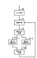
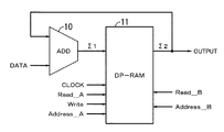
図1は、本発明の動作原理を説明する原理図である。この図に示すように、本発明の演算装置は、入力手段20、演算手段21、書き込み手段22、第1の格納手段23−1、第2の格納手段23−2、および、読み出し手段24によって構成されている。なお、この原理図は、n=2に対応している。
【0024】
ここで、入力手段20は、演算対象となるデータ群を入力する。
演算手段21は、読み出し手段24によって読み出されたデータ群と、入力手段20から新たに入力されたデータ群との間で所定の演算を行う。
【0025】
書き込み手段22は、演算手段21の演算結果を、読み出し手段24が読み出し対象としていない所定の格納手段に対して書き込む。
第1の格納手段23−1および第2の格納手段23−2は、データ群の少なくとも一部又は全部を格納することが可能な容量を有している。
【0026】
読み出し手段24は、第1の格納手段23−1および第2の格納手段23−2の何れかを選択し、既に格納されているデータ群を読み出す。
次に、以上の原理図の動作について説明する。
【0027】
先ず、演算処理を実行する前に、第1の格納手段23−1および第2の格納手段23−2の双方を初期値“0”により初期化する。
次に、入力手段20は、第1番目のデータ群の入力を開始する。このとき、読み出し手段24は、第1の格納手段23−1のアドレス“0000”に格納されているデータ(いまの例では、初期値“0”)を読み出し、演算手段21に供給している。従って、演算手段21は、入力手段20から入力されたデータと、読み出し手段24から供給されたデータを加算し、書き込み手段22に供給する。いまの例では、読み出し手段24から供給されるデータは、初期値“0”であるので、入力されたデータがそのまま書き込み手段22に対して供給されることになる。
【0028】
書き込み手段22は、演算手段21から出力されたデータを、読み出しの対象となっていない第2の格納手段23−2のアドレス“0000”に対して書き込む。
【0029】
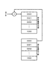
図2は、以上の動作の概要を説明するための図である。この図に示すように、第1の格納手段23−1のアドレス“0000”から読み出されたデータ(いまの例では初期値“0”)は、入力されたデータ群の第1番目のデータと加算され、第2の格納手段23−2のアドレス“0000”に格納されることになる。
【0030】
次に、第1番目のデータ群の第2番目のデータが入力手段20から入力されると、読み出し手段24は、第1の格納手段23−1のアドレス“0001”からデータを読み出し、演算手段21に供給する。
【0031】
演算手段21は、入力手段20から供給されたデータと、読み出し手段24から供給されたデータを加算し、書き込み手段22に供給する。
書き込み手段22は、第2の格納手段23−2のアドレス“0001”に対して、演算手段21から供給されたデータを格納する。
【0032】
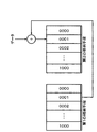
図3は、以上の動作の概要を説明するための図である。この図に示すように、第1の格納手段23−1のアドレス“0001”から読み出されたデータ(いまの例では初期値“0”)は、入力されたデータ群の第2番目のデータと加算され、第2の格納手段23−2のアドレス“0001”に格納されることになる。
【0033】
以上の動作は、格納手段23−1,23−2の最大アドレス(この例ではアドレス“1000”)まで繰り返される。その結果、入力手段20から入力された第1番目のデータ群の全てが、第2の格納手段23−2のアドレス“0000”からアドレス“1000”のそれぞれに格納される。
【0034】
第1番目のデータ群に対する処理が終了すると、書き込み手段22および読み出し手段24は、書き込みまたは読み出しの対象となる格納手段を交換する。即ち、書き込み手段22は、第1の格納手段23−1を書き込みの対象とし、また、読み出し手段24は、第2の格納手段23−2を読み出しの対象とする。
【0035】
入力手段20から第2番目のデータ群の第1番目のデータが入力されると、演算手段21は、読み出し手段24から供給されたデータと、入力手段20から供給されたデータとを加算し、書き込み手段22に供給する。このとき、読み出し手段24は、第2の格納手段23−2のアドレス“0000”に格納されているデータを読み出して供給しているので、演算手段21は、第2の格納手段23−2のアドレス“0000”に格納されているデータ(第1番目のデータ群の第1番目のデータ)と、入力手段20から入力された第2番目のデータ群の第1番目のデータとを加算し、書き込み手段22に供給する。
【0036】
書き込み手段22は、演算手段21から供給されたデータを、第1の格納手段23−1のアドレス“0000”に格納する。
図4は、以上の動作の概要を説明する図である。この図に示すように、第2の格納手段23−2のアドレス“0000”から読み出されたデータ(いまの例では第1番目のデータ群の第1番目のデータ)は、入力された第2のデータ群の第1番目のデータと加算され、第1の格納手段23−1のアドレス“0000”に格納されることになる。
【0037】
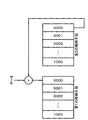
次に、第2番目のデータ群の第2番目のデータが入力手段20から入力されると、読み出し手段24は、第2の格納手段23−2のアドレス“0001”に格納されているデータ(第1のデータ群の第2番目のデータ)を読み出し、演算手段21に供給する。
【0038】
演算手段21は、入力手段20から入力されたデータと、読み出し手段24から供給されたデータとを加算し、得られた結果を書き込み手段22に供給する。いまの例では、読み出し手段24からは第1のデータ群の第2番目のデータが供給され、また、入力手段20からは第2番目のデータ群の第2番目のデータが供給されるので、これらのデータが加算された値が、書き込み手段22に供給されることになる。
【0039】
書き込み手段22は、演算手段21から供給されたデータを、第1の格納手段23−1のアドレス“0001”に格納する。
図5は、以上の動作の概要を説明する図である。この図に示すように、第2の格納手段23−2のアドレス“0001”から読み出されたデータ(いまの例では第1番目のデータ群の第2番目のデータ)は、入力された第2番目のデータ群の第2番目のデータと加算され、第1の格納手段23−1のアドレス“0001”に格納されることになる。
【0040】
以上の動作は、格納手段23−1,23−2の最大アドレス(この例ではアドレス“1000”)まで繰り返される。その結果、入力手段20から入力された第2番目のデータ群のそれぞれは、第2の格納手段23−2に格納されているデータ群の対応するデータと加算され、第1の格納手段23−1の対応するアドレスに格納されることになる。
【0041】
そして、第2番目のデータ群に対する処理が終了すると、第3番目のデータ群に対する処理が実行される。第3番目のデータ群に対する処理では、図2および図3に示す場合と同様に、第1の格納手段23−1に格納されているデータ(第1番目のデータ群と第2番目のデータ群が加算されたデータ)と、入力手段20から新たに入力された第3番目のデータ群とが順次加算され、第2の格納手段23−2に順次格納されることになる。
【0042】
第3番目のデータ群に対する処理が終了すると、続いて、第4番目のデータ群に対する処理が実行され、全てのデータ群に対する処理が終了するまで同様の動作が繰り返される。
【0043】
そして、最後のデータ群である第m番目のデータ群に対する処理が完了すると、書き込み手段23−1が最後に書き込みの対象とした格納手段(第1または第2の格納手段)には、第1〜第m番目のデータ群のそれぞれのデータを累積加算(積分)したデータが格納されている。
【0044】
このようなデータを利用することにより、例えば、W−CDMA方式の携帯電話システムにおいて、基地局との相関値を算出することができる。
以上に説明したように、本発明の演算装置によれば、第1乃至第n(図1の例ではn=2)の格納手段を設け、所定の格納手段からそれまでのデータ群を累積加算値を読み出しながら、新たに入力されたデータ群との加算処理を行い、得られた結果を他の格納手段に格納するようにしたので、格納手段として、例えば、SP−RAMを使用することが可能になる。従って、演算装置のサイズを小型化するとともに、DP−RAMを使用した場合と同様に高速な演算処理を実現することが可能になる。
【0045】
なお、以上の原理図では、第1の格納手段23−1および第2の格納手段23−2の2つの格納手段を設けるようにしたが、3以上の格納手段を設けることも可能である。
【0046】
また、以上の実施の形態では、入力手段20から入力されたデータ群の全てに対して演算を施し、第1の格納手段23−1および第2の格納手段23−2に格納するようにしたが、これらの一部のみに対して演算を施し、第1の格納手段23−1および第2の格納手段23−2に格納するようにすることも可能である。
【0047】
次に、本発明の実施の形態について説明する。
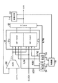
図6は、本発明の実施の形態の構成例を示す図である。この図に示すように、本発明の演算装置は、ADD50、記憶部51、セレクタ52、初期化部53、アドレス発生部54、R/W制御部55、および、制御部56によって構成されている。
【0048】
ADD50は、入力されたデータ(DATA)と、セレクタ52から供給されたデータを加算し、SP−RAM51bに供給する。
記憶部51は、SP−RAM51aおよびSP−RAM51bによって構成されている。ここで、記憶部51は、R/W制御部55から供給される制御信号によって指定されるSP−RAMであって、アドレス発生部54から供給されたアドレス信号の値に対応するアドレスに格納されているデータを読み出して出力するとともに、データの読み出しの対象となっていないSP−RAMであって、アドレス発生部54から供給されたアドレス信号の値に対応するアドレスに対してADD50の演算結果を格納する。
【0049】
セレクタ52は、R/W制御部55によって読み出しの対象として指定されたSP−RAMを選択し、出力されるデータを初期化部53に供給する。
初期化部53は、第1番目のデータ群が入力された場合には、セレクタ52から出力されるデータを全て“0”に初期化し、ADD50に供給する。
【0050】
アドレス発生部54は、制御部56の制御に従って、アドレス信号を発生し、記憶部51のSP−RAM51a,51bのそれぞれに供給する。
R/W制御部55は、制御部56の制御に従って、SP−RAM51aおよびSP−RAM51bの何れか一方を読み出し対象として指定し、他方を書き込み対象として指定する。
【0051】
制御部56は、アドレス発生部54、R/W制御部55、および、セレクタ52を制御する。
次に、以上の実施の形態の動作について説明する。
【0052】
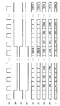
図7は、本発明の実施の形態の動作を説明するタイミングチャートである。以下、この図を随時参照しながら、図6に示す実施の形態の動作について説明する。
【0053】
先ず、制御部56は、図7(A)に示すクロック信号のパルスの立ち上がりエッジに同期して、初期化部53に対して初期化を指示する。また、制御部56は、アドレス発生部54に対してアドレス信号を発生するように指示するとともに、R/W制御部55に対してR/W信号を発生するように指示する。
【0054】
アドレス発生部54は、制御部56からの指示を受け、“0”から最大アドレス“10239”までカウントアップし、最大値に達した場合には、“0”に循環する動作を行う。また、アドレス発生部54から出力されるアドレス信号の最上位のビット(MSB)には、SP−RAM51aまたはSP−RAM51bの何れかを読み出し対象(または書き込み対象)として指定するための信号を含んでいる。なお、SP−RAM51aとSP−RAM51bには、上位ビット(MSB)を除外したアドレス信号がADD1およびADD2として供給されるので、これらのアドレス信号は“0”から“10239”までの値を循環する信号となる(図7(E),(F)参照)。
【0055】
R/W制御部55は、アドレス発生部54から供給されるデータのMSBが“0”である場合には、R/W1信号を“L”に、R/W2信号を“H”に、また、R/W3信号を“L”の状態にする。また、アドレス発生部54から供給されるデータのMSBが“1”である場合には、R/W1信号を“H”に、R/W2信号を“L”に、また、R/W3信号を“H”の状態にする(図7(B)〜(D)参照)。
【0056】
いま、ADD50に対するデータ群の供給が開始されたとすると、ADD50は、初期化部53から供給されたデータΣ2と、入力されたデータ(“100”:図7(G)参照)とを加算して出力する。いまの例では、初期化部53は制御部56から初期化処理を指示されているので、データΣ2としては、セレクタ52から出力されるデータの値に拘わらず、“0”がADD50に供給される(図7(I)参照)。
【0057】
ADD50は、入力されたデータ(=“100”)と、初期化部53から供給されたデータ(=“0”)とを加算し、データΣ1として出力する。このとき、アドレス発生部54は、SP−RAM51aと、SP−RAM51bに対して、値“0”を有するアドレス信号ADD1,ADD2を出力している。また、アドレス信号のMSBは“0”であり、R/W制御部55は、R/W1信号として“L”を、R/W2信号として“H”を、また、R/W3信号として“L”を出力する(図7(B)〜(D)参照)。
【0058】
その結果、SP−RAM51aは読み出し状態に、SP−RAM51bは書き込み状態に設定され、また、セレクタ52はSP−RAM51aからの出力を選択する状態になる。
【0059】
従って、ADD50から出力されたデータ“100”は、SP−RAM51bのアドレス“0”に格納されることになる。
続いて、次のクロック信号の立ち上がりエッジが到来すると、アドレス発生部54はアドレス値を“1”だけインクリメントし、値“1”を有するアドレス信号ADD1,ADD2を生成し、SP−RAM51aとSP−RAM51bにそれぞれ供給する。
【0060】
このとき、アドレス信号のMSBは変化しないので、SP−RAM51aは読み出しの対象となり、SP−RAM51bは書き込みの対象となる。更に、初期化部53からは、“0”が出力されるので、ADD50は入力されたデータ“150”(図7(G)参照)に対して“0”を加算して得られた値“150”を、SP−RAM51bのアドレス“1”に対して書き込む。
【0061】
以上の動作は、アドレス値が“10239”になるまで繰り返される。その結果、SP−RAM51bには、入力されたデータ群がそのまま格納されることになる。
【0062】
続いて、アドレス発生部54は、MSBを“1”に設定するとともに、それ以外のビットを全て“0”に設定する。その結果、R/W制御部55は、R/W1信号を“H”の状態に、R/W2信号を“L”の状態に、また、R/W3信号を“H”の状態に設定するので、SP−RAM51aが書き込み状態に、SP−RAM51bが読み出し状態に、また、セレクタ52はSP−RAM51bからの出力を選択して出力する状態になる。
【0063】
なお、このとき、制御部56は、初期化部53に対して初期化を終了するように指示するので、初期化部53は、セレクタ52から出力されたデータを、そのまま、ADD50に供給する。
【0064】
このような状態において、第2番目のデータ群が入力されると、SP−RAM51bは、アドレス“0”に格納されているデータ(第1番目のデータ群の第1番目のデータ“100”)を読み出して出力する。
【0065】
セレクタ52は、SP−RAM51bから供給されたデータを選択し、初期化部53に供給する。
初期化部53は、セレクタ52から出力されたデータ“100”をそのままADD50に供給する。ADD50は、初期化部53から出力されたデータ“100”と、新たに入力されたデータ“477”とを加算し、得られたデータ“577”を、SP−RAM51aのアドレス“0”に格納する。
【0066】
続いて、アドレス発生部54は、アドレス値を“1”だけインクリメントし、得られた値“1”を有するアドレス信号ADD1,ADD2を出力する。その結果、SP−RAM51bのアドレス“1”からは、先に格納されたデータ“150”が読み出され、セレクタ52および初期化部53を介してADD50に供給される。
【0067】
ADD50は、新たに入力されたデータ“144”と、初期化部53から供給されたデータ“150”とを加算し、得られたデータ“294”を、SP−RAM51aに供給する。
【0068】
SP−RAM51aは、供給されたデータ“294”をアドレス“1”に格納する。
以上の処理は、アドレス値が“10239”になるまで繰り返される。その結果、SP−RAM51aには、第1番目のデータ群と、第2番目のデータ群のそれぞれのデータを加算した値が格納されることになる。
【0069】
続いて、MSBが“0”に設定されるとともに、MSB以外のビットが“0”に設定され、SP−RAM51aを読み出し対象とし、また、SP−RAM51bを書き込み対象として演算処理が実行される。
【0070】
以上の処理は、制御部56によって予め設定された回数だけ繰り返され、全てのデータの加算が終了した場合には、最後の演算結果が格納された何れかのSP−RAMからデータを読み出すことにより、演算結果を取得することが可能になる。
【0071】
以上に説明したように、本実施の形態によれば、SP−RAMを複数設け、これらを交互に読み出し側および書き込み側として使用し、入力されたデータ群を累積加算するようにしたので、演算処理を高速に実行することが可能になるとともに、SP−RAMの使用により装置のサイズを小型化することが可能になる。
【0072】
なお、以上の実施の形態においては、演算回数は固定の場合を例に挙げて説明したが、動作状況に応じて演算回数を変更するようにしてもよい。そのような実施の形態によれば、積分の時間(積分対象となるデータ)を、動作中に変更することが可能になる。
【0073】
また、ブロック単位での演算の回数を計数し、その回数が所定の値になった場合には、演算処理を停止するようにしてもよい。そのような実施の形態によれば、設定された値に応じてデータの積分を行うことが可能になる。
【0074】
また、前述のブロック単位での演算回数を、動作状況その他に応じて変更することも可能である。そのような実施の形態によれば、使用目的または使用環境に応じて最適な動作が可能になる。
【0075】
また、以上の実施の形態では、SP−RAMが2つの場合について説明したが、これらが3以上であってもよい。なお、その場合には、アドレス信号の上位の複数ビットを使用することにより、所望のSP−RAMを選択することができる。
【0076】
また、以上の実施の形態では、MSBを選択用のビットとして使用したが、LSBその他のビットを使用することができることはいうまでもない。
また、以上の実施の形態では、セレクタ52とADD50の間に初期化部53を設け、初回の演算時において初期化を行うようにしたが、本発明は、このような場合のみに限定されるものではなく、これ以外にも種々の変形実施例が想定できることはいうまでもない。要は、初回の演算時において、ADD50から出力されるデータが、入力データと等しくなるようにすればよい。
【0077】
また、以上の実施の形態では、データ群間の演算処理として、加算を行う場合を例に挙げて説明したが、本発明はこのような場合のみに限定されるものではなく、例えば、減算その他を行うことも可能であることはいうまでもない。
【0078】
また、本実施の形態では、同一の値を有するアドレスに対するデータの読み出し動作と、書き込み動作とを並行して行うようにしたが、ADD50等における遅延を考慮して、読み出し動作を先行して行うことも可能である。
【0079】
また、本実施の形態では、演算装置単体として説明を行ったが、このような演算装置を、例えば、携帯電話等の受信装置に内蔵することも可能であることはいうまでもない。
【0080】
(付記1) 複数のデータから構成されるデータ群を入力し、先に入力された他のデータ群との間で所定の演算処理を実行する演算装置において、
前記データ群をデータを入力する入力手段と、
前記データ群の少なくとも一部又は全部を格納することが可能な容量を各々有する第1乃至第n(n>1)の格納手段と、
前記第1乃至第nの格納手段の何れかを選択し、既に格納されているデータ群を読み出す読み出し手段と、
前記読み出し手段によって読み出されたデータ群と、前記入力手段から新たに入力されたデータ群との間で所定の演算を行う演算手段と、
前記演算手段の演算結果を、前記読み出し手段が読み出しの対象として選択していない所定の格納手段に対して書き込む書き込み手段と、
を有することを特徴とする演算装置。
【0081】
(付記2) 前記第1乃至第nの格納手段の何れかに格納されている演算結果のデータを出力する出力手段を更に有することを特徴とする付記1記載の演算装置。
【0082】
(付記3) 前記第1乃至第nの格納手段は、メモリアレイによって構成されており、前記メモリアレイをバンク形式で切り換えて前記第1乃至第nの格納手段として使用することを特徴とする付記1記載の演算装置。
【0083】
(付記4) 前記メモリアレイはシングルポートメモリから構成されることを特徴とする付記3記載の演算装置。
(付記5) 前記読み出し手段および前記書き込み手段がアクセスするアドレスを発生するアドレス発生手段を更に有し、
前記アドレス発生手段が発生するアドレスの所定のビットにより、前記第1乃至第nの格納手段のうち、前記読み出し手段および前記書き込み手段がそれぞれアクセスすべき格納手段を特定することを特徴とする付記3記載の演算装置。
【0084】
(付記6) 前記読み出し手段は、前記書き込み手段の書き込みより先行してデータを読み出すことを特徴とする付記1記載の演算装置。
(付記7) 前記演算手段は、加算処理を行うことにより、前記データ群単位で積分演算を実行することを特徴とする付記1記載の演算装置。
【0085】
(付記8) 演算処理を開始することを指示する演算開始指示手段と、
前記演算開始指示手段によって演算の開始が指示された場合には、前記読み出し手段から供給される第1番目のデータ群の全てのデータを初期値“0”に設定する初期化手段と、
を有することを特徴とする付記1記載の演算装置。
【0086】
(付記9) ブロック単位での演算の回数を計数する計数手段と、
前記計数手段によって計数された値が所定の設定値になった場合には演算処理を停止する停止手段と、
を更に有することを特徴とする付記1記載の演算装置。
【0087】
(付記10) 前記設定値を変更する設定値変更手段を更に有することを特徴とする付記9記載の演算装置。
(付記11) 複数のデータから構成されるデータ群を受信し、先に受信した他のデータ群との間で所定の演算処理を実行する受信装置において、
前記データ群をデータを入力する入力手段と、
前記データ群の少なくとも一部又は全部を格納することが可能な容量を有する第1乃至第n(n>1)の格納手段と、
前記第1乃至第nの格納手段の何れかを選択し、既に格納されているデータ群を読み出す読み出し手段と、
前記読み出し手段によって読み出されたデータ群と、前記入力手段から新たに入力されたデータ群との間で所定の演算を行う演算手段と、
前記演算手段の演算結果を、前記読み出し手段が読み出しの対象としていない所定の格納手段に対して書き込む書き込み手段と、
を有することを特徴とする受信装置。
【0088】
【発明の効果】
以上説明したように本発明では、複数のデータから構成されるデータ群を入力し、先に入力された他のデータ群との間で所定の演算処理を実行する演算装置において、データ群を入力する入力手段と、データ群の少なくとも一部又は全部を格納することが可能な容量を有する第1乃至第n(n>1)の格納手段と、第1乃至第nの格納手段の何れかを選択し、既に格納されているデータ群を読み出す読み出し手段と、読み出し手段によって読み出されたデータ群と、入力手段から新たに入力されたデータ群との間で所定の演算を行う演算手段と、演算手段の演算結果を、読み出し手段が読み出しの対象としていない所定の格納手段に対して書き込む書き込み手段と、を設けるようにしたので、演算を高速に実行するとともに、装置のサイズを小型化することができる。
【0089】
また、複数のデータから構成されるデータ群を受信し、先に受信した他のデータ群との間で所定の演算処理を実行する受信装置において、データ群を入力する入力手段と、データ群の少なくとも一部又は全部を格納することが可能な容量を有する第1乃至第n(n>1)の格納手段と、第1乃至第nの格納手段の何れかを選択し、既に格納されているデータ群を読み出す読み出し手段と、読み出し手段によって読み出されたデータ群と、入力手段から新たに入力されたデータ群との間で所定の演算を行う演算手段と、演算手段の演算結果を、読み出し手段が読み出しの対象としていない所定の格納手段に対して書き込む書き込み手段と、を設けるようにしたので、データを高速に受信するとともに、装置のサイズを小型化することが可能になる。
【図面の簡単な説明】
【図1】本発明の動作原理を説明する原理図である。
【図2】図1に示す原理図の動作を説明するための図である。
【図3】図1に示す原理図の動作を説明するための図である。
【図4】図1に示す原理図の動作を説明するための図である。
【図5】図1に示す原理図の動作を説明するための図である。
【図6】本発明の実施の形態の構成例を示す図である。
【図7】図6に示す実施の形態の動作を説明するためのタイミングチャートである。
【図8】従来の演算装置の構成例を示す図である。
【図9】図8に示す演算装置の動作を説明するための図である。
【符号の説明】
10 ADD
11 DP−RAM
20 入力手段
21 演算手段
22 書き込み手段
23−1 第1の格納手段
23−2 第2の格納手段
24 読み出し手段
50 ADD
51 記憶部
51a SP−RAM
51b SP−RAM
52 セレクタ
53 初期化部
54 アドレス発生部
55 R/W制御部
56 制御部[0001]
BACKGROUND OF THE INVENTION
The present invention is a computing device. And receiving device In particular, the present invention relates to an arithmetic device and a receiving device that input a data group composed of a plurality of data and execute predetermined arithmetic processing with another previously input data group.
[0002]
[Prior art]
In the field of information processing, there is a case where a data group composed of a plurality of data is input and a predetermined calculation process is performed with another previously input data group.
[0003]
Such a calculation is used, for example, in integrating a received signal in units of one slot when calculating a correlation value with a base station in a W-CDMA (Wideband Code Division Multiple Access) mobile phone system. .
[0004]
FIG. 8 is a diagram illustrating a configuration example of a conventional integration circuit used in W-CDMA. As shown in this figure, the conventional integrating circuit is composed of an ADD (Adder) 10 and a DP-RAM (Dual Port Random Access Memory) 11.
[0005]
Here, the
[0006]
The DP-
[0007]
The DP-
Next, the operation of the above conventional example will be described.
[0008]
First, when the first data group is input, the output data from the DP-
[0009]
The data output from the
[0010]
As a result, the first data group is stored as it is with respect to each of the maximum addresses from the address “0000”.
Subsequently, when the second data group is input, the DP-
[0011]
The ADD 10 adds the top data of the second data group and the top data of the first data group supplied from the DP-
[0012]
At this time, since the Write signal is active, and the Address_A signal outputs a signal designating the address “0000” of the DP-
[0013]
Since the timing for reading data Σ2 precedes the timing for writing data Σ1 by one clock, data Σ2 is overwritten by data Σ1 and data Σ2 is not lost.
[0014]
FIG. 9 is a diagram for briefly explaining the operation of the conventional arithmetic unit.
As shown in this figure, the data Σ2 read one clock before from the address “0000” of the DP-
[0015]
A similar operation is executed between the next input data and the data stored at the address “0001”, and the calculation result data Σ1 is stored at the address “0001”.
[0016]
By repeating the above operation a predetermined number of times, it is possible to sequentially add the input data group and output the obtained result as an integral value.
[0017]
[Problems to be solved by the invention]
By the way, since the conventional arithmetic device described above uses the DP-
[0018]
As a result, there has been a problem that it is difficult to reduce the size of a receiving device such as a mobile phone equipped with such an arithmetic device.
The present invention has been made in view of the above situation, and is an arithmetic device capable of high-speed operation and downsizing of the device. And receiving device The purpose is to provide.
[0019]
[Means for Solving the Problems]
In the present invention, in order to solve the above-described problem, an operation for inputting a data group composed of a plurality of data shown in FIG. 1 and executing a predetermined operation process with another previously input data group is performed. In the apparatus, input means 20 for inputting the data group and first to nth (n> 1) storage means 23-1 to 23-1 having a capacity capable of storing at least part or all of the data group. 23-2 and any one of the first to n-th storage units 23-1 to 23-2, and a
[0020]
Here, the input means 20 inputs a data group. The first to nth (n> 1) storage means 23-1 to 23-2 have a capacity capable of storing at least a part or all of the data group. The
[0021]
Further, in a receiving device that receives a data group composed of a plurality of data and executes predetermined arithmetic processing with another data group received earlier, an input means for inputting the data group, and the data The first to nth (n> 1) storage means having a capacity capable of storing at least part or all of the group and the first to nth storage means are selected and stored. A reading means for reading the data group being read, a calculation means for performing a predetermined calculation between the data group read by the reading means, and a data group newly input from the input means, and the calculation means There is provided a receiving device comprising: a writing unit for writing the calculation result into a predetermined storage unit not read by the reading unit.
[0022]
Here, the input means inputs a data group. The first to nth (n> 1) storage means have a capacity capable of storing at least part or all of the data group. The reading unit selects any one of the first to nth storage units and reads a data group already stored. The calculation means performs a predetermined calculation between the data group read by the reading means and the data group newly input from the input means. The writing unit writes the calculation result of the calculation unit into a predetermined storage unit that is not read by the reading unit.
[0023]
DETAILED DESCRIPTION OF THE INVENTION
Hereinafter, embodiments of the present invention will be described with reference to the drawings.
FIG. 1 is a principle diagram illustrating the operating principle of the present invention. As shown in this figure, the arithmetic device of the present invention includes an input means 20, an
[0024]
Here, the input means 20 inputs a data group to be calculated.
The calculating means 21 performs a predetermined calculation between the data group read by the reading means 24 and the data group newly input from the input means 20.
[0025]
The
The first storage unit 23-1 and the second storage unit 23-2 have a capacity capable of storing at least a part or all of the data group.
[0026]
The
Next, the operation of the above principle diagram will be described.
[0027]
First, before executing the arithmetic processing, both the first storage means 23-1 and the second storage means 23-2 are initialized with the initial value “0”.
Next, the input means 20 starts to input the first data group. At this time, the
[0028]
The
[0029]
FIG. 2 is a diagram for explaining the outline of the above operation. As shown in this figure, the data read from the address “0000” of the first storage means 23-1 (in this example, the initial value “0”) is the first data of the input data group. And is stored in the address “0000” of the second storage means 23-2.
[0030]
Next, when the second data of the first data group is inputted from the input means 20, the reading means 24 reads the data from the address “0001” of the first storage means 23-1, and calculates the computing means. 21.
[0031]
The computing means 21 adds the data supplied from the input means 20 and the data supplied from the reading means 24 and supplies the result to the writing means 22.
The writing means 22 stores the data supplied from the computing means 21 at the address “0001” of the second storage means 23-2.
[0032]
FIG. 3 is a diagram for explaining the outline of the above operation. As shown in this figure, the data read from the address “0001” of the first storage means 23-1 (in this example, the initial value “0”) is the second data of the input data group. And is stored in the address “0001” of the second storage means 23-2.
[0033]
The above operation is repeated up to the maximum address of the storage means 23-1 and 23-2 (in this example, the address “1000”). As a result, all the first data groups input from the
[0034]
When the processing for the first data group is completed, the writing means 22 and the reading means 24 exchange storage means to be written or read. That is, the
[0035]
When the first data of the second data group is input from the
[0036]
The writing means 22 stores the data supplied from the computing means 21 at the address “0000” of the first storage means 23-1.
FIG. 4 is a diagram for explaining the outline of the above operation. As shown in this figure, the data read from the address “0000” of the second storage means 23-2 (the first data in the first data group in the present example) is inputted. The first data of the second data group is added and stored in the address “0000” of the first storage means 23-1.
[0037]
Next, when the second data of the second data group is input from the
[0038]
The
[0039]
The
FIG. 5 is a diagram for explaining the outline of the above operation. As shown in this figure, the data read from the address “0001” of the second storage means 23-2 (the second data in the first data group in the present example) is inputted. It is added to the second data of the second data group and stored in the address “0001” of the first storage means 23-1.
[0040]
The above operation is repeated up to the maximum address of the storage means 23-1 and 23-2 (in this example, the address “1000”). As a result, each of the second data group input from the
[0041]
Then, when the process for the second data group is completed, the process for the third data group is executed. In the process for the third data group, the data stored in the first storage means 23-1 (the first data group and the second data group, as in the case shown in FIGS. 2 and 3). And the third data group newly input from the input means 20 are Sequentially Added to the second storage means 23-2 Sequentially Will be stored.
[0042]
First 3 When processing for the second data group is completed, 4 The processing for the second data group is executed, and the same operation is repeated until the processing for all the data groups is completed.
[0043]
When the processing for the m-th data group, which is the last data group, is completed, the storage means (first or second storage means) to which the writing means 23-1 finally writes is the first Stores data obtained by cumulative addition (integration) of each data of the m-th data group.
[0044]
By using such data, for example, in a W-CDMA mobile phone system, a correlation value with a base station can be calculated.
As described above, according to the arithmetic unit of the present invention, the first to n-th (n = 2 in the example of FIG. 1) storage means are provided, and the data group from the predetermined storage means to the cumulative addition is provided. Since the addition process with the newly input data group is performed while reading the value and the obtained result is stored in another storage means, for example, SP-RAM can be used as the storage means. It becomes possible. Therefore, it is possible to reduce the size of the arithmetic device and realize high-speed arithmetic processing as in the case where the DP-RAM is used.
[0045]
In the above principle diagram, two storage units, the first storage unit 23-1 and the second storage unit 23-2, are provided, but it is also possible to provide three or more storage units.
[0046]
Further, in the above embodiment, all the data groups input from the
[0047]
Next, an embodiment of the present invention will be described.
FIG. 6 is a diagram illustrating a configuration example of the embodiment of the present invention. As shown in this figure, the arithmetic device of the present invention is composed of an
[0048]
The
The
[0049]
The
When the first data group is input, the
[0050]
The
The R /
[0051]
The
Next, the operation of the above embodiment will be described.
[0052]
FIG. 7 is a timing chart for explaining the operation of the embodiment of the present invention. The operation of the embodiment shown in FIG. 6 will be described below with reference to this figure as needed.
[0053]
First, the
[0054]
The
[0055]
When the MSB of the data supplied from the
[0056]
Assuming that the supply of the data group to the
[0057]
The
[0058]
As a result, the SP-
[0059]
Therefore, the data “100” output from the
Subsequently, when the rising edge of the next clock signal arrives, the
[0060]
At this time, since the MSB of the address signal does not change, the SP-
[0061]
The above operation is repeated until the address value becomes “10239”. As a result, the input data group is stored as it is in the SP-
[0062]
Subsequently, the
[0063]
At this time, since the
[0064]
In such a state, when the second data group is input, the SP-
[0065]
The
The
[0066]
Subsequently, the
[0067]
The
[0068]
The SP-
The above processing is repeated until the address value becomes “10239”. As a result, the SP-
[0069]
Subsequently, the MSB is set to “0” and the bits other than the MSB are set to “0”, and the arithmetic processing is executed with the SP-
[0070]
The above processing is repeated a predetermined number of times by the
[0071]
As described above, according to this embodiment, a plurality of SP-RAMs are provided, and these are alternately used as the read side and the write side, and the input data group is cumulatively added. The processing can be executed at high speed, and the size of the apparatus can be reduced by using the SP-RAM.
[0072]
In the above embodiment, the case where the number of calculations is fixed has been described as an example. However, the number of calculations may be changed according to the operation state. According to such an embodiment, the integration time (data to be integrated) can be changed during operation.
[0073]
Further, the number of operations in units of blocks may be counted, and the calculation process may be stopped when the number of times reaches a predetermined value. According to such an embodiment, it is possible to perform integration of data according to a set value.
[0074]
It is also possible to change the number of operations in units of blocks as described above according to the operation status and the like. According to such an embodiment, an optimal operation can be performed according to the purpose of use or usage environment.
[0075]
Moreover, although the above embodiment demonstrated the case where there were two SP-RAMs, these may be three or more. In this case, a desired SP-RAM can be selected by using a plurality of upper bits of the address signal.
[0076]
In the above embodiment, the MSB is used as a selection bit. However, it goes without saying that LSB and other bits can be used.
In the above embodiment, the
[0077]
In the above embodiment, the case where addition is performed as an example of arithmetic processing between data groups has been described as an example. However, the present invention is not limited to such a case. It goes without saying that it is also possible to carry out.
[0078]
In the present embodiment, the same Have a value Although the data read operation and the write operation for the address are performed in parallel, the read operation can be performed in advance in consideration of a delay in the
[0079]
In the present embodiment, the arithmetic device is described as a single unit. However, it goes without saying that such an arithmetic device can also be incorporated in a receiving device such as a mobile phone.
[0080]
(Additional remark 1) In the arithmetic unit which inputs the data group comprised from several data, and performs a predetermined arithmetic process between the other data groups input previously,
Input means for inputting data into the data group;
Capacity capable of storing at least a part or all of the data group Each First to nth (n> 1) storage means comprising:
A reading unit that selects any one of the first to n-th storage units and reads a data group that has already been stored;
Arithmetic means for performing a predetermined operation between the data group read by the reading means and the data group newly input from the input means;
The result of calculation by the calculation means is read by the reading means. Select Writing means for writing to the predetermined storage means,
An arithmetic device comprising:
[0081]
(Supplementary note 2) The arithmetic unit according to
[0082]
(Supplementary Note 3) The first to nth storage means include Memory array Said
[0083]
(Appendix 4) Memory array Is single port memory Consists of The arithmetic unit according to supplementary note 3, wherein:
(Additional remark 5) It further has an address generation means which generates the address which the said reading means and the said writing means access,
Supplementary note 3 wherein the storage means to be accessed by the reading means and the writing means among the first to nth storage means is specified by a predetermined bit of the address generated by the address generating means. The computing device described.
[0084]
(Supplementary Note 6) The reading means is the writing means. Writing The arithmetic unit according to
(Additional remark 7) The said calculating means performs the integral calculation per said data group by performing an addition process, The arithmetic unit of
[0085]
(Supplementary Note 8) Calculation start instruction means for instructing to start calculation processing;
When the start of calculation is instructed by the calculation start instruction means, the first data group supplied from the reading means All data of Initializing means for setting the initial value to “0”;
The arithmetic unit according to
[0086]
(Supplementary Note 9) Counting means for counting the number of operations in block units;
Stop means for stopping the arithmetic processing when the value counted by the counting means reaches a predetermined set value;
The arithmetic unit according to
[0087]
(Supplementary note 10) The arithmetic unit according to supplementary note 9, further comprising setting value changing means for changing the setting value.
(Additional remark 11) In the receiver which receives the data group comprised from several data, and performs a predetermined arithmetic process between the other data groups received previously,
Input means for inputting data into the data group;
First to nth (n> 1) storage means having a capacity capable of storing at least part or all of the data group;
A reading unit that selects any one of the first to n-th storage units and reads a data group that has already been stored;
Arithmetic means for performing a predetermined operation between the data group read by the reading means and the data group newly input from the input means;
A writing unit for writing the calculation result of the calculation unit to a predetermined storage unit that is not read by the reading unit;
A receiving apparatus comprising:
[0088]
【The invention's effect】
As described above, in the present invention, a data group composed of a plurality of data is input, and the data group is input in an arithmetic device that executes predetermined arithmetic processing with another previously input data group. Input means, first to nth (n> 1) storage means having a capacity capable of storing at least part or all of the data group, and any of the first to nth storage means. A reading means for selecting and reading a data group already stored; a computing means for performing a predetermined calculation between the data group read by the reading means and the data group newly input from the input means; Since there is provided a writing means for writing the calculation result of the calculation means to a predetermined storage means that is not read by the reading means, the calculation is executed at a high speed and the size of the apparatus is reduced. It is possible to type of.
[0089]
Further, in a receiving device that receives a data group composed of a plurality of data and executes predetermined arithmetic processing with other data groups received earlier, an input means for inputting the data group, One of the first to nth (n> 1) storage means and the first to nth storage means having a capacity capable of storing at least part or all of them is selected and already stored. Reading means for reading a data group, a data group read by the reading means, a calculation means for performing a predetermined calculation between the data group newly input from the input means, and a calculation result of the calculation means are read Since the means is provided with the writing means for writing to the predetermined storage means that are not to be read, it is possible to receive data at high speed and to reduce the size of the apparatus. .
[Brief description of the drawings]
FIG. 1 is a principle diagram illustrating an operation principle of the present invention.
FIG. 2 is a diagram for explaining the operation of the principle diagram shown in FIG. 1;
3 is a diagram for explaining the operation of the principle diagram shown in FIG. 1; FIG.
4 is a diagram for explaining the operation of the principle diagram shown in FIG. 1; FIG.
FIG. 5 is a diagram for explaining the operation of the principle diagram shown in FIG. 1;
FIG. 6 is a diagram illustrating a configuration example of an embodiment of the present invention.
7 is a timing chart for explaining the operation of the embodiment shown in FIG. 6;
FIG. 8 is a diagram illustrating a configuration example of a conventional arithmetic device.
9 is a diagram for explaining the operation of the arithmetic device shown in FIG. 8;
[Explanation of symbols]
10 ADD
11 DP-RAM
20 Input means
21 Calculation means
22 Writing means
23-1 First storage means
23-2 Second storage means
24 Reading means
50 ADD
51 Storage unit
51a SP-RAM
51b SP-RAM
52 selector
53 Initialization section
54 Address generator
55 R / W controller
56 Control unit
Claims (7)
前記データ群を入力する入力部と、
前記データ群のうち少なくとも一部を格納可能な第1記憶部と、
前記データ群のうち少なくとも一部を格納可能な第2記憶部と、
前記第1記憶部および前記第2記憶部のいずれか一方を読み出し対象として指定し、他方を書き込み対象として指定するリードライト制御部と、
アドレス信号を発生するアドレス発生部と、
読み出し対象として指定された前記第1記憶部または前記第2記憶部から、前記アドレス信号に対応するアドレスに格納されているデータを読み出すセレクタ部と、
一の前記データ群については、前記入力部から入力されたデータと等しい出力データを、他の前記データ群については前記入力部から入力されたデータと前記セレクタ部から読み出したデータを加算した出力データを、書き込み対象として指定された前記第1記憶部または前記第2記憶部に対し、前記アドレス信号に対応するアドレスに格納する加算器と、 を有することを特徴とする演算装置。In an arithmetic unit that inputs a data group composed of a plurality of data and executes predetermined arithmetic processing with another data group that has been input in advance,
An input unit for inputting the data group;
A first storage unit capable of storing at least a part of the data group;
A second storage unit capable of storing at least a part of the data group;
A read / write control unit that designates one of the first storage unit and the second storage unit as a read target and the other as a write target;
An address generator for generating an address signal;
A selector unit that reads data stored in an address corresponding to the address signal from the first storage unit or the second storage unit that is designated as a read target;
Output data equal to the data input from the input unit for one data group, and output data obtained by adding data input from the input unit and data read from the selector unit for the other data group And an adder that stores, at the address corresponding to the address signal, the first storage unit or the second storage unit designated as a write target .
前記加算器は、一の前記データ群について、前記入力部から入力されたデータと前記初期化部が初期化して供給したデータとを加算した出力データを格納することを特徴とする請求項1記載の演算装置。 An initialization unit for initializing data read by the selector unit;
The said adder stores the output data which added the data input from the said input part, and the data which the said initialization part initialized and supplied about one said data group. Arithmetic unit.
前記データ群を入力する入力部と、 An input unit for inputting the data group;
前記データ群のうち少なくとも一部を格納可能な第1記憶部と、 A first storage unit capable of storing at least a part of the data group;
前記データ群のうち少なくとも一部を格納可能な第2記憶部と、 A second storage unit capable of storing at least a part of the data group;
前記第1記憶部および前記第2記憶部のいずれか一方を読み出し対象として指定し、他方を書き込み対象として指定するリードライト制御部と、 A read / write control unit that designates one of the first storage unit and the second storage unit as a read target and the other as a write target;
アドレス信号を発生するアドレス発生部と、 An address generator for generating an address signal;
読み出し対象として指定された前記第1記憶部または前記第2記憶部から、前記アドレス信号に対応するアドレスに格納されているデータを読み出すセレクタ部と、 A selector unit that reads data stored in an address corresponding to the address signal from the first storage unit or the second storage unit that is designated as a read target;
一の前記データ群については、前記入力部から入力されたデータと等しい出力データを、他の前記データ群については前記入力部から入力されたデータと前記セレクタ部から読み出したデータを加算した出力データを、書き込み対象として指定された前記第1記憶部または前記第2記憶部に対し、前記アドレス信号に対応するアドレスに格納する加算器と、 を有することを特徴とする受信装置。 Output data equal to the data input from the input unit for one data group, and output data obtained by adding data input from the input unit and data read from the selector unit for the other data group And an adder that stores, at the address corresponding to the address signal, the first storage unit or the second storage unit that is designated as a write target.
Priority Applications (4)
| Application Number | Priority Date | Filing Date | Title |
|---|---|---|---|
| JP2001204162A JP4278317B2 (en) | 2001-07-05 | 2001-07-05 | Arithmetic device and receiving device |
| US10/078,368 US6947961B2 (en) | 2001-07-05 | 2002-02-21 | Arithmetic unit and receiver unit |
| DE60235139T DE60235139D1 (en) | 2001-07-05 | 2002-03-11 | Computing unit and receiving unit |
| EP20020251691 EP1274006B1 (en) | 2001-07-05 | 2002-03-11 | Arithmetic unit and receiver unit |
Applications Claiming Priority (1)
| Application Number | Priority Date | Filing Date | Title |
|---|---|---|---|
| JP2001204162A JP4278317B2 (en) | 2001-07-05 | 2001-07-05 | Arithmetic device and receiving device |
Publications (3)
| Publication Number | Publication Date |
|---|---|
| JP2003015862A JP2003015862A (en) | 2003-01-17 |
| JP2003015862A5 JP2003015862A5 (en) | 2006-10-05 |
| JP4278317B2 true JP4278317B2 (en) | 2009-06-10 |
Family
ID=19040669
Family Applications (1)
| Application Number | Title | Priority Date | Filing Date |
|---|---|---|---|
| JP2001204162A Expired - Fee Related JP4278317B2 (en) | 2001-07-05 | 2001-07-05 | Arithmetic device and receiving device |
Country Status (4)
| Country | Link |
|---|---|
| US (1) | US6947961B2 (en) |
| EP (1) | EP1274006B1 (en) |
| JP (1) | JP4278317B2 (en) |
| DE (1) | DE60235139D1 (en) |
Families Citing this family (3)
| Publication number | Priority date | Publication date | Assignee | Title |
|---|---|---|---|---|
| US7394561B2 (en) * | 2002-08-28 | 2008-07-01 | Kabushiki Kaisha Toshiba | Image forming apparatus |
| JP4765260B2 (en) * | 2004-03-31 | 2011-09-07 | 日本電気株式会社 | Data processing device, processing method thereof, program, and mobile phone device |
| JP4724031B2 (en) * | 2006-03-28 | 2011-07-13 | 三菱プレシジョン株式会社 | Computer and computer system using synchronized stack memory |
Family Cites Families (11)
| Publication number | Priority date | Publication date | Assignee | Title |
|---|---|---|---|---|
| DE3066955D1 (en) * | 1980-06-24 | 1984-04-19 | Ibm | Signal processor computing arrangement and method of operating said arrangement |
| US4689762A (en) * | 1984-09-10 | 1987-08-25 | Sanders Associates, Inc. | Dynamically configurable fast Fourier transform butterfly circuit |
| JPH0520139A (en) | 1991-07-15 | 1993-01-29 | Hokkaido Nippon Denki Software Kk | Source unit deleting system |
| JPH0566751A (en) | 1991-09-10 | 1993-03-19 | Matsushita Electric Ind Co Ltd | Gradation correcting circuit |
| US5371877A (en) * | 1991-12-31 | 1994-12-06 | Apple Computer, Inc. | Apparatus for alternatively accessing single port random access memories to implement dual port first-in first-out memory |
| GB2291515B (en) * | 1994-07-14 | 1998-11-18 | Advanced Risc Mach Ltd | Data processing using multiply-accumulate instructions |
| US6061783A (en) * | 1996-11-13 | 2000-05-09 | Nortel Networks Corporation | Method and apparatus for manipulation of bit fields directly in a memory source |
| JP2760352B1 (en) * | 1996-11-29 | 1998-05-28 | 日本電気株式会社 | Cell search circuit for CDMA |
| DE69837299T2 (en) * | 1997-01-22 | 2007-06-28 | Matsushita Electric Industrial Co., Ltd., Kadoma | System and method for fast Fourier transformation |
| US6191998B1 (en) * | 1997-10-16 | 2001-02-20 | Altera Corporation | Programmable logic device memory array circuit having combinable single-port memory arrays |
| US6363060B1 (en) * | 1999-06-30 | 2002-03-26 | Qualcomm Incorporated | Method and apparatus for fast WCDMA acquisition |
-
2001
- 2001-07-05 JP JP2001204162A patent/JP4278317B2/en not_active Expired - Fee Related
-
2002
- 2002-02-21 US US10/078,368 patent/US6947961B2/en not_active Expired - Lifetime
- 2002-03-11 EP EP20020251691 patent/EP1274006B1/en not_active Expired - Lifetime
- 2002-03-11 DE DE60235139T patent/DE60235139D1/en not_active Expired - Lifetime
Also Published As
| Publication number | Publication date |
|---|---|
| US20030009499A1 (en) | 2003-01-09 |
| JP2003015862A (en) | 2003-01-17 |
| EP1274006A2 (en) | 2003-01-08 |
| EP1274006B1 (en) | 2010-01-20 |
| EP1274006A3 (en) | 2005-11-16 |
| DE60235139D1 (en) | 2010-03-11 |
| US6947961B2 (en) | 2005-09-20 |
Similar Documents
| Publication | Publication Date | Title |
|---|---|---|
| CN112712457B (en) | Data processing method and artificial intelligence processor | |
| JP4278317B2 (en) | Arithmetic device and receiving device | |
| JP3656876B2 (en) | Synchronous semiconductor memory device having macroinstruction function and method for storing and executing macroinstruction | |
| JP3587675B2 (en) | Pseudo noise generator | |
| US7035318B2 (en) | Receiving unit and semiconductor device | |
| JPH11110339A (en) | DMA controller | |
| JP2000349681A (en) | Spread spectrum communication receiver | |
| GB2344980A (en) | Digital matched filter correlates received spread spectrum signals to save power. | |
| US6922764B2 (en) | Memory, processor system and method for performing write operations on a memory region | |
| JP2003332945A (en) | Common data path rake receiver for CDMA demodulator circuit | |
| KR100854037B1 (en) | Multipath Explorer for Asynchronous Base Station Modems | |
| JP2502857B2 (en) | Signal processor | |
| JP3166781B2 (en) | Adder circuit | |
| JP3126430B2 (en) | Pattern generation circuit | |
| KR100525549B1 (en) | Read Address Counting Apparutus and its method in Block Interleaver | |
| JP3557895B2 (en) | Memory clear device | |
| JPH09265381A (en) | Time switch memory data controller | |
| JPH0832837A (en) | Gamma correction circuit | |
| WO2001089126A1 (en) | Receiver and inverse-spreading code generating method | |
| JP2005167814A (en) | Correlation processing circuit | |
| KR20010008761A (en) | Fast viterbi decoder for cdma mobile station employing parallel add-select-compare and traceback architecture | |
| JP2003087221A (en) | CDMA reception demodulation apparatus and CDMA reception demodulation method | |
| JP2003101454A (en) | Communication data storage address acquisition circuit | |
| JPH0620195B2 (en) | Speed conversion circuit | |
| JP2006211403A (en) | Error correction device |
Legal Events
| Date | Code | Title | Description |
|---|---|---|---|
| A521 | Written amendment |
Free format text: JAPANESE INTERMEDIATE CODE: A523 Effective date: 20060816 |
|
| A621 | Written request for application examination |
Free format text: JAPANESE INTERMEDIATE CODE: A621 Effective date: 20060816 |
|
| A711 | Notification of change in applicant |
Free format text: JAPANESE INTERMEDIATE CODE: A712 Effective date: 20080730 |
|
| A131 | Notification of reasons for refusal |
Free format text: JAPANESE INTERMEDIATE CODE: A131 Effective date: 20081111 |
|
| A521 | Written amendment |
Free format text: JAPANESE INTERMEDIATE CODE: A523 Effective date: 20090109 |
|
| TRDD | Decision of grant or rejection written | ||
| A01 | Written decision to grant a patent or to grant a registration (utility model) |
Free format text: JAPANESE INTERMEDIATE CODE: A01 Effective date: 20090310 |
|
| A01 | Written decision to grant a patent or to grant a registration (utility model) |
Free format text: JAPANESE INTERMEDIATE CODE: A01 |
|
| A61 | First payment of annual fees (during grant procedure) |
Free format text: JAPANESE INTERMEDIATE CODE: A61 Effective date: 20090310 |
|
| FPAY | Renewal fee payment (event date is renewal date of database) |
Free format text: PAYMENT UNTIL: 20120319 Year of fee payment: 3 |
|
| R150 | Certificate of patent or registration of utility model |
Ref document number: 4278317 Country of ref document: JP Free format text: JAPANESE INTERMEDIATE CODE: R150 Free format text: JAPANESE INTERMEDIATE CODE: R150 |
|
| FPAY | Renewal fee payment (event date is renewal date of database) |
Free format text: PAYMENT UNTIL: 20120319 Year of fee payment: 3 |
|
| S531 | Written request for registration of change of domicile |
Free format text: JAPANESE INTERMEDIATE CODE: R313531 |
|
| S533 | Written request for registration of change of name |
Free format text: JAPANESE INTERMEDIATE CODE: R313533 |
|
| FPAY | Renewal fee payment (event date is renewal date of database) |
Free format text: PAYMENT UNTIL: 20120319 Year of fee payment: 3 |
|
| R350 | Written notification of registration of transfer |
Free format text: JAPANESE INTERMEDIATE CODE: R350 |
|
| FPAY | Renewal fee payment (event date is renewal date of database) |
Free format text: PAYMENT UNTIL: 20130319 Year of fee payment: 4 |
|
| FPAY | Renewal fee payment (event date is renewal date of database) |
Free format text: PAYMENT UNTIL: 20140319 Year of fee payment: 5 |
|
| S111 | Request for change of ownership or part of ownership |
Free format text: JAPANESE INTERMEDIATE CODE: R313111 |
|
| R350 | Written notification of registration of transfer |
Free format text: JAPANESE INTERMEDIATE CODE: R350 |
|
| LAPS | Cancellation because of no payment of annual fees |