JP4274751B2 - Encoder - Google Patents
Encoder Download PDFInfo
- Publication number
- JP4274751B2 JP4274751B2 JP2002193448A JP2002193448A JP4274751B2 JP 4274751 B2 JP4274751 B2 JP 4274751B2 JP 2002193448 A JP2002193448 A JP 2002193448A JP 2002193448 A JP2002193448 A JP 2002193448A JP 4274751 B2 JP4274751 B2 JP 4274751B2
- Authority
- JP
- Japan
- Prior art keywords
- signal
- origin
- phase
- origin detection
- signals
- Prior art date
- Legal status (The legal status is an assumption and is not a legal conclusion. Google has not performed a legal analysis and makes no representation as to the accuracy of the status listed.)
- Expired - Fee Related
Links
Images


Classifications
-
- G—PHYSICS
- G01—MEASURING; TESTING
- G01D—MEASURING NOT SPECIALLY ADAPTED FOR A SPECIFIC VARIABLE; ARRANGEMENTS FOR MEASURING TWO OR MORE VARIABLES NOT COVERED IN A SINGLE OTHER SUBCLASS; TARIFF METERING APPARATUS; MEASURING OR TESTING NOT OTHERWISE PROVIDED FOR
- G01D5/00—Mechanical means for transferring the output of a sensing member; Means for converting the output of a sensing member to another variable where the form or nature of the sensing member does not constrain the means for converting; Transducers not specially adapted for a specific variable
- G01D5/26—Mechanical means for transferring the output of a sensing member; Means for converting the output of a sensing member to another variable where the form or nature of the sensing member does not constrain the means for converting; Transducers not specially adapted for a specific variable characterised by optical transfer means, i.e. using infrared, visible, or ultraviolet light
- G01D5/32—Mechanical means for transferring the output of a sensing member; Means for converting the output of a sensing member to another variable where the form or nature of the sensing member does not constrain the means for converting; Transducers not specially adapted for a specific variable characterised by optical transfer means, i.e. using infrared, visible, or ultraviolet light with attenuation or whole or partial obturation of beams of light
- G01D5/34—Mechanical means for transferring the output of a sensing member; Means for converting the output of a sensing member to another variable where the form or nature of the sensing member does not constrain the means for converting; Transducers not specially adapted for a specific variable characterised by optical transfer means, i.e. using infrared, visible, or ultraviolet light with attenuation or whole or partial obturation of beams of light the beams of light being detected by photocells
- G01D5/347—Mechanical means for transferring the output of a sensing member; Means for converting the output of a sensing member to another variable where the form or nature of the sensing member does not constrain the means for converting; Transducers not specially adapted for a specific variable characterised by optical transfer means, i.e. using infrared, visible, or ultraviolet light with attenuation or whole or partial obturation of beams of light the beams of light being detected by photocells using displacement encoding scales
- G01D5/34707—Scales; Discs, e.g. fixation, fabrication, compensation
- G01D5/34715—Scale reading or illumination devices
-
- G—PHYSICS
- G01—MEASURING; TESTING
- G01D—MEASURING NOT SPECIALLY ADAPTED FOR A SPECIFIC VARIABLE; ARRANGEMENTS FOR MEASURING TWO OR MORE VARIABLES NOT COVERED IN A SINGLE OTHER SUBCLASS; TARIFF METERING APPARATUS; MEASURING OR TESTING NOT OTHERWISE PROVIDED FOR
- G01D5/00—Mechanical means for transferring the output of a sensing member; Means for converting the output of a sensing member to another variable where the form or nature of the sensing member does not constrain the means for converting; Transducers not specially adapted for a specific variable
- G01D5/12—Mechanical means for transferring the output of a sensing member; Means for converting the output of a sensing member to another variable where the form or nature of the sensing member does not constrain the means for converting; Transducers not specially adapted for a specific variable using electric or magnetic means
- G01D5/244—Mechanical means for transferring the output of a sensing member; Means for converting the output of a sensing member to another variable where the form or nature of the sensing member does not constrain the means for converting; Transducers not specially adapted for a specific variable using electric or magnetic means influencing characteristics of pulses or pulse trains; generating pulses or pulse trains
- G01D5/245—Mechanical means for transferring the output of a sensing member; Means for converting the output of a sensing member to another variable where the form or nature of the sensing member does not constrain the means for converting; Transducers not specially adapted for a specific variable using electric or magnetic means influencing characteristics of pulses or pulse trains; generating pulses or pulse trains using a variable number of pulses in a train
- G01D5/2454—Encoders incorporating incremental and absolute signals
- G01D5/2455—Encoders incorporating incremental and absolute signals with incremental and absolute tracks on the same encoder
- G01D5/2457—Incremental encoders having reference marks
-
- G—PHYSICS
- G01—MEASURING; TESTING
- G01D—MEASURING NOT SPECIALLY ADAPTED FOR A SPECIFIC VARIABLE; ARRANGEMENTS FOR MEASURING TWO OR MORE VARIABLES NOT COVERED IN A SINGLE OTHER SUBCLASS; TARIFF METERING APPARATUS; MEASURING OR TESTING NOT OTHERWISE PROVIDED FOR
- G01D5/00—Mechanical means for transferring the output of a sensing member; Means for converting the output of a sensing member to another variable where the form or nature of the sensing member does not constrain the means for converting; Transducers not specially adapted for a specific variable
- G01D5/26—Mechanical means for transferring the output of a sensing member; Means for converting the output of a sensing member to another variable where the form or nature of the sensing member does not constrain the means for converting; Transducers not specially adapted for a specific variable characterised by optical transfer means, i.e. using infrared, visible, or ultraviolet light
- G01D5/32—Mechanical means for transferring the output of a sensing member; Means for converting the output of a sensing member to another variable where the form or nature of the sensing member does not constrain the means for converting; Transducers not specially adapted for a specific variable characterised by optical transfer means, i.e. using infrared, visible, or ultraviolet light with attenuation or whole or partial obturation of beams of light
- G01D5/34—Mechanical means for transferring the output of a sensing member; Means for converting the output of a sensing member to another variable where the form or nature of the sensing member does not constrain the means for converting; Transducers not specially adapted for a specific variable characterised by optical transfer means, i.e. using infrared, visible, or ultraviolet light with attenuation or whole or partial obturation of beams of light the beams of light being detected by photocells
- G01D5/36—Forming the light into pulses
- G01D5/366—Particular pulse shapes
Landscapes
- Physics & Mathematics (AREA)
- General Physics & Mathematics (AREA)
- Transmission And Conversion Of Sensor Element Output (AREA)
- Optical Transform (AREA)
Description
【0001】
【発明の属する技術分野】
本発明は、エンコーダに係り、特に、変位検出に用いられるエンコーダに関する。
【0002】
【従来の技術】
従来の技術によるエンコーダの一般的な例としては、光学式のエンコーダが知られている。
【0003】
即ち、この光学式のエンコーダは、LED等の発光部と該発光部からのビーム光を平行光にするための光学素子とを組み合わせた光源部と、該光源部からの平行光が順次に照射されるインデックススケールおよびスケールと、該スケールから見て光源部の反対側に配置された光検出器と、該光検出器からの信号を処理してエンコーダ信号として出力する信号処理回路部とから構成されている。
【0004】
このような構成において、インデックススケール、スケール、光検出部は、位置検出用、及び、原点検出用の部分からなる。
【0005】
即ち、インデックススケール、スケールには、位置検出用、及び、原点検出用のスリット部が設けられているとともに、光検出部にも位置検出用、及び、原点検出用の光検出部が設けられており、これらの組合せにより、位置検出・原点検出が可能となっている。
【0006】
そして、ステージやモータなどの位置検出を行う対象物において、上記光源部と光検出器との組合せは、可動部と固定部のうちの、どちらか一方に取り付けられる。
【0007】
また、スケールは、可動部と固定部のうちどちらか他方に取り付けられる。
【0008】
また、一般的なエンコーダ出力信号には、以下のものがある。
【0009】
まず、装置などの可動部の変位に伴って出力される互いに90°位相の異なる正弦波信号、または、パルス(矩形波)信号であるA相信号とB相信号、さらに、可動部の基準位置検出の際に出力されるZ相信号(原点検出用信号)である。
【0010】
また、装置の電源を投入したり、位置情報をクリアした時点で可動部の絶対位置が不明な場合には、原点検出を行うことによって正確な位置情報を得ることができる。
【0011】
そして、エンコーダのうち、直線的な位置検出を行うリニアエンコーダでは、直状スケールの一端近傍に原点検出用パターンを配置することが多い。
【0012】
また、回転運動を検出するロータリエンコーダでは、通常、円盤状スケール上の1箇所に原点検出用パターンを配置する。
【0013】
そして、可動部を動かしてスケールの原点検出用パターンを検出し、必要に応じてAB相信号との同期をとって原点信号を出力するようになされている。
【0014】
例えば、特開平8−261795号公報では、図26に示すように、スケール・インデックススケール・受光部に、位置検出信号より周期の長い信号を発生させて検出する機構を設けている。
【0015】
即ち、図26においては、光源31からの光を平行光にするコリメータレンズ32と、メインスケ−ル33とが備えられている。
【0016】
メインスケ−ル33には、変位信号生成用のパターン34と、基準位置信号生成用のスリットパターン35と、基準位置補助信号生成用のスリットパターン39とが設けられている。
【0017】
また、メインスケ−ル33と相対移動する移動体または固定体に固定し、メインスケール33に対向するように配置されたインデックススケール36には、90°づつ位相の異なる変位信号を生成するために4か所に設けたスリットパターン71〜74と、基準位置信号生成用のスリットパターン38と、基準位置補助信号生成用のスリットパターン75、76とが形成されている。
【0018】
そして、インデックススケール36の光源側に対して、それの反対側には、変位信号用の受光素子51〜54と、基準信号用の受光素子55と、基準位置補助信号用の受光素子61、62とが設けられている。
【0019】
これにより、変位信号と基準位置信号の他に基準位置補助信号を発生させ、原点信号を位置検出信号に同期させる際の指標としている。
【0020】
【発明が解決しようとする課題】
近年、エンコーダの高分解能・高精度化が進む中で、原点信号の精度に対しても要求が高まり、AB相信号と同等の分解能・精度や、タイミングもAB相信号と同期して出すことが要求として挙がってきている。即ち、検出幅が狭く、しかも再現性の良い原点信号が求められている。従って、システムとしての不安定要素による原点検出精度の劣化や検出タイミングのずれを抑えることがエンコーダに求められてきている。
【0021】
なお、不安定要素には、信号ノイズやふらつき、さらには、光学式のエンコーダでは光源の安定性、発光・受光素子の温度特性とそのばらつきやステージのガタツキやギャップ・取付け角度の経時変化といった、組み込むステージの原点検出時のヘッドとスケールの配置や姿勢の変動などがある。
【0022】
特に、AB相信号とZ相信号を別個の光学系などで検出しながら原点検出をAB相に同期させる場合、A相またはB相信号とZ相信号の位相を正確に同期させたり、適切な位相差を持たせなければ、検出タイミングのずれにより、AB相信号の1周期分ずれた位置を原点とする可能性がある。
【0023】
光学式のエンコーダでは、これらの問題を解決するために原点検出のための補助信号発生用部材を設けることが多い。しかしながら、部材・特殊な光学系の追加やスケールパターンの追加により、ヘッドサイズやスケール幅を大きくする必要が生じたり、コストの上昇につながりかねず、小型化・低コスト化の流れに反するものになりやすい。
【0024】
本発明は、上記の事情に鑑みてなされたもので、特に、変位検出に用いられるエンコーダにおいて、AB相に同期した原点検出が安定して行えるエンコーダを提供することを目的とする。
【0025】
【課題を解決するための手段】
本発明によると、上記課題を解決するために、(1)移動体の位置又は角度の変位に応じて周期信号を発生する位置信号発生手段と、上記移動体が所定の位置にある場合に原点信号を発生する原点検出手段と、原点信号の発生位置を上記周期信号が所定の位相を取る位置に同期させる同期手段と、予め定められた複数の位相の1つを上記所定の位相として選択し切り替え可能な選択手段と、上記複数の位相の内、最適な位相を検知する判定手段と、を有し、上記選択手段は、上記判定手段からの判定結果に基づいて原点信号の発生位置において上記周期信号が取る位相を選択可能とする、ことを特徴とするエンコーダが提供される。
【0027】
また、本発明によると、上記課題を解決するために、(2)上記移動体が所定の範囲にある場合に原点検出用信号を発生する原点検出用信号発生手段を有し、上記判定手段は、原点検出用信号発生時に上記周期信号が取る位相と原点信号発生位置で上記周期信号が取り得る位相との位相差に基づき上記最適な位相を検知する、ことを特徴とする(1)に記載のエンコーダが提供される。
【0028】
また、本発明によると、上記課題を解決するために、(3)上記判定手段は、上記原点検出用信号発生時に上記周期信号が取る位相と上記原点信号発生位置で上記周期信号が取り得る位相との位相差を0°〜180°で表した時に、位相差が最も大きくなる上記周期信号が取り得る位相を最適と判定する、ことを特徴とする(2)に記載のエンコーダが提供される。
【0029】
また、本発明によると、上記課題を解決するために、(4)90°位相差の2つの上記周期信号と2つの上記複数の位相を有し、該2つ位相の位相差が180°である、ことを特徴とする(1)乃至(3)の何れかに記載のエンコーダが提供される。
【0030】
また、本発明によると、上記課題を解決するために、(5)上記移動体の位置又は角度の変位に伴い、上記周期信号、または、デジタル化された上記周期信号が、その振幅中央値を値の低い側から値の高い側へ交差する位相、または、値の高い側から値の低い側へ交差する位相を上記原点検出位置での上記周期信号の位相とする、ことを特徴とする(4)に記載のエンコーダが提供される。
【0031】
また、本発明によると、上記課題を解決するために、(6)90°位相差の2つの上記周期信号とN個(Nは3以上の整数)の上記複数の位相を有し、該N個の上記複数の位相の位相差が(360°/N)置きとなるように配置される、ことを特徴とする(1)乃至(3)の何れかに記載のエンコーダが提供される。
【0033】
また、本発明によると、上記課題を解決するために、(7)移動体の位置又は角度の変位に応じて90°位相差の2つの周期信号を発生する位置信号発生手段と、上記移動体が所定の範囲にある場合に原点検出用信号を発生する原点検出用信号発生手段と、上記移動体が所定の位置にある場合に原点信号を発生する原点検出手段と、原点信号の発生位置を上記周期信号が所定の位相を取る位置に同期させる同期手段と、予め定められた複数の位相の1つを上記所定の位相として選択し切り替え可能な選択手段と、上記複数の位相の内、最適な位相を検知する判定手段と、を有し、2次元の直交座標系の横軸方向に上記2つの周期信号の一方の出力を、縦軸方向に他方の出力を取り、上記座標系上で上記2つの周期信号のそれぞれの出力によって決まる点が移動体の変位につれて描く波形を上記2つの周期信号のリサージュ波形としたとき、上記2つの周期信号のリサージュ波形を、分割してできる2つ以上の複数の区分を有し、上記2つの周期信号で決まる点が含まれる区分が、少なくとも上記原点検出用信号発生時に判別でき、上記判定手段は、原点検出用信号発生時に上記2つの周期信号によって決まる点が存在するリサージュ波形上の上記区分に基づき上記判定手段での判定を行い、上記選択手段は、上記判定手段からの判定結果に基づいて原点信号の発生位置において上記周期信号が取る位相を選択可能とする、ことを特徴とするエンコーダが提供される。
【0034】
また、本発明によると、上記課題を解決するために、(8)上記原点検出用信号発生時に上記2つの周期信号によって決まる点が存在するリサージュ波形上の区分と上記周期信号の複数の位相との位相差を0°〜180°で表す時に、上記区分と各位相との組合せについて、区分内での位相差の最小値を該区分と位相との位相差とした時、上記判定手段が、位相差が最も大きくなる位相を最適と判定する、ことを特徴とする(7)に記載のエンコーダが提供される。
【0035】
また、本発明によると、上記課題を解決するために、(9)複数の原点検出用信号を発生させるための原点検出用信号発生手段を有し、上記複数の位相のそれぞれの位相は上記複数の原点検出用信号の1つに対応し、選択手段により上記周期信号の所定の位相と対応する原点検出用信号を同時に選択し、選択した上記周期信号の所定の位相と対応する原点検出用信号を用いて原点信号を発生させる、ことを特徴とする(1)乃至(8)の何れかに記載のエンコーダが提供される。
【0036】
また、本発明によると、上記課題を解決するために、(10)複数の上記周期信号を有し、上記複数の位相は複数の上記周期信号の周期信号ごとに決められた所定の位相に対応し、選択手段により上記周期信号の所定の位相の1つを選択し、原点信号発生位置を選択した上記周期信号の所定の位相に同期可能である、ことを特徴とする(1)乃至(9)の何れかに記載のエンコーダが提供される。
【0037】
また、本発明によると、上記課題を解決するために、(11)移動体の位置又は角度の変位に応じて発生する周期信号に基づき変位量を検出し、上記移動体が所定の範囲にある場合に原点信号を発生するエンコーダであって、光源からの光を移動体に設けられたスケールに照射し帰還した光を受光部で受光して、上記移動体の位置変位を検出する検出手段と、上記光源、または、別に設けた光源からの光を上記スケールに照射し帰還した光を別に設けた受光部で受光する受光手段と、上記移動体が所定の範囲にある場合に原点検出用信号を発生する原点検出用信号発生手段と、上記全ての光源及び全ての受光部が半導体プロセスにより同一基板上に所定の間隔で配置・形成されることにより、原点検出用信号発生時での上記周期信号の位相と原点信号発生位置での上記周期信号の位相の位相差が所定の値となるように構成され、原点信号の発生位置を上記周期信号が所定の位相を取る位置に同期させる同期手段と、を有することを特徴とするエンコーダが提供される。
【0042】
また、本発明によると、上記課題を解決するために、
(18) 上記検知した最適な同期位置を記憶する記憶手段を更に有することを特徴とする(9)乃至(17)の何れかに記載のエンコーダが提供される。
【0043】
以上のような解決手段の構成において、後述する実施の形態の構成とは、次のように対応している。
【0044】
移動体:スケール4
位置信号発生手段:光源部10からスケール4のスリット4aを経由した光を受光する光検出部5a
原点検出用信号発生手段:光源部10からスケール4のスリット4bを経由した光を受光する光検出部5b
原点検出回路:信号処理回路部(原点検出回路部)6
選択手段:スイッチ104
判定手段:判定回路107
記憶手段:記憶器109
【0045】
【発明の実施の形態】
以下、図面を参照して本発明の実施の形態について説明する。
【0046】
(第1の実施の形態)
[構成]
本発明の第1の実施の形態によるエンコーダの主要部の構成は、信号処理回路部を除き、位置信号(位置検出信号)と原点検出用信号とが得られるものであれば、特に、限定されない。
【0047】
例えば、図25に示したような光学式のエンコーダによる構成など一般的なものを適用することができる。
【0048】
また、図25の例では光学式のエンコーダを挙げているが、磁気式など他のタイプでもよい。
【0049】
即ち、図25に示すように、この光学式のエンコーダは、LED等の発光部1と該発光部1からのビーム光を平行光にするための光学素子2とを組み合わせた光源部10と、該光源部10からの平行光が順次に照射されるインデックススケール3及びスケール4と、該スケール4から見て光源部10の反対側に配置された光検出器5と、該光検出器5からの信号を処理してエンコーダ信号として出力する信号処理回路部6とから構成されている。
【0050】
このような構成において、インデックススケール3、スケール4、光検出器5のうち、位置検出用に用いられるのは、インデックススケール3に形成されているスリット3aと、スケール4に形成されているスリット4aと、光検出器5に形成されている光検出部5aとの組合せである。
【0051】
また、原点検出用に用いられるのは、インデックススケール3に形成されているスリット3bと、スケール4に形成されているスリット4bと、光検出器5に形成されている光検出部5bとの組合せである。
【0052】
ステージやモータなどの位置検出を行う対象物においては、上記光源部10と光検出器5との組合せは、それらの可動部と固定部のうち、どちらか一方に取り付けられる。
【0053】
また、スケール4は、それらの可動部と固定部のうち、どちらか他方に取り付けられる。
【0054】
ここで、光検出部5aの受光素子からは、スケール4の移動に対応して互いに位相が90°異なる信号(A(+)、A(−)、B(+)、B(−))が出力されるが、後述する図2では説明の簡単化のため、A(+)信号を位置信号(a)、B(+)信号を位置信号(b)として、もしくは、[A(+)−A(−)]信号を位置信号(a)、[B(+)−B(−)]信号を位置信号(b)として表示し、他の信号については表示しないものとしている。
【0055】
なお、光検出部5bの受光素子からは、可動部の基準位置検出の際に出力されるZ相信号としての原点検出用信号(e)が出力される。
【0056】
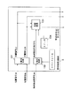
図1は、本発明の第1の実施の形態による図25のエンコーダにおける信号処理回路部6の構成を示すブロック図である。
【0057】
この信号処理回路部6は、アナログ位置信号(a),(b)をデジタル位置信号(c),(d)に変換するための2値化回路101と、原点検出用信号(e)を所定のスライスレベルで2値化してデジタル原点検出用信号(f)に変換する2値化回路102と、この2値化回路102からのデジタル原点検出用信号(f)を2値化回路101からのデジタル位置信号(c),(d)に同期させて原点信号(g)または(h)を発生させる同期回路103と、この同期回路103における同期のタイミングを切り替えるスイッチ104とからなる。
【0058】
図1においては、デジタル位置信号(c),(d)に同期させて原点信号(g)または(h)を得ているが、アナログ位置信号(a),(b)に同期させて原点信号(g)または(h)を得ることも同様の機能で実現できる。
【0059】
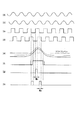
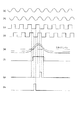
[作用]
図2は、図1の信号処理回路部6によって、図25に示したような光検出器5からの入力が処理されている様子を示すタイムチャートである。図2において、横軸は時間を表し、一定速度の変位が生じているときの各信号の変化を示している。
【0060】
まず、2値化回路101において、変位に伴い周期的に変化するエンコーダのアナログ位置信号(a),(b)を2値化することによってデジタル位置信号(c),(d)が得られる。
【0061】
また、2値化回路102において、原点検出用信号(e)を所定のスライスレベルで2値化することによって、デジタル原点検出用信号(f)が得られる。
【0062】
そして、原点信号については、次の2つの方法のうちから1つを選択することで得られる。
【0063】
1つ目は、同期回路103において、デジタル原点検出用信号(f)を位置信号(a),(c)の立ち上がりに同期させてハイレベルとし、位置信号(b),(d)のレベル変化に同期させてローレベルとすることで、原点信号(g)を得るものである。
【0064】
2つ目は、同期回路103において、デジタル原点検出用信号(f)を位置信号(a),(c)の立ち下がりに同期させてハイレベルとし、位置信号(b),(d)のレベル変化に同期させてローレベルとすることで、原点信号(h)を得るものである。
【0065】
これら2つのうちの1つを選択して原点信号(g)または(h)として出力するが、この選択はスイッチ104により行う。
【0066】
ここで、位置信号(a),(b)と(c),(d)の組合せは、90°の位相差を持つ。
【0067】
また、アナログ信号である位置信号(a),(b)と原点検出用信号(e)とは、デジタル信号である位置信号(c),(d)と原点検出用信号(f)を作り出すことができるものであれば、それらがどのようなタイプの信号でも構わない。また、図25に示したような光検出器5からの入力がデジタル信号のみで、アナログ信号を含まなくても構わない。また、入力されるアナログの位置信号をデジタル化する際には、さらに、位相分割により分解能を向上させたものとしても構わない。
【0068】
そして、位置検出は、デジタル位置信号(c),(d)を図示しないカウンタに入力することによって行う。この場合、原点信号(g)または(h)が発生したときに、カウンタをリセットすることによって、位置検出の原点出しが可能となる。
【0069】
以上のように、原点検出用信号(e)をデジタル化してデジタル原点検出用信号(f)をつくり、デジタル原点検出用信号(f)と周期信号である位置信号(c)や(d)とを同期させて原点信号(g)または(h)を生成するようにしている。
【0070】
このとき、1回の原点検出において、1周期条件を満足するタイミングが複数回あっても、原点信号(g)または(h)は最先の条件満足タイミングでのみ生成されるように構成されているものとする。
【0071】
これは、後述する各実施の形態でも同様とする。
【0072】
[効果]
原点検出用信号の出力の仕方に応じて位置信号との同期位置を選択することが可能である。
【0073】
従って、信号ノイズやふらつき、さらには、光学式のエンコーダでは光源の安定性、発光・受光素子の温度特性とそのばらつき、個々のエンコーダの設計とのずれなどの不安定要素によって生じ得る原点検出位置のずれを少なくする同期位置を選択することが可能である。
【0074】
例えば、上記不安定要素により、図2の原点検出用信号(e)の出力レベルが上がったり、図中左方向にシフトしたり、スライスレベルが若干下がることが考えられる。このとき、原点検出用信号(e)が太線から細線のように変化したとすると、デジタル原点検出用信号(f)は破線のようになる。これにより、原点信号(h)においては破線で示した1周期分ずれた位置が原点信号として検出される。これに対して、原点信号(g)ではこのような変化は起きにくい。従って、この場合には、原点信号(g)を選択することによって、原点検出精度の劣化を抑え、安定した原点検出が可能となる。
【0075】
また、この例では、信号処理回路部6を除いて、原点検出のための補助信号発生用部材などを設けていない。従って、安定した原点検出ができ、且つ、小型で安価なエンコーダを供給することが可能である。
【0076】
(第2の実施の形態)
[構成]
この第2の実施の形態の主要部の構成は、第1の実施の形態と同様に、信号処理回路部6を除き、位置信号と原点検出用信号が得られるものであれば、特に、限定されない。例えば、前述した第1の実施の形態の主要部の構成として図25に示したような光学式のエンコーダ構成など一般的なものでよい。また、図25の例では光学式のエンコーダを挙げているが、磁気式など他のタイプでもよい。
【0077】
また、本発明の第2の実施の形態による図25のエンコーダにおける信号処理回路部6の構成については、図1に示したブロック図と同様のものでよい。
【0078】
なお、図1においては、デジタル位置信号(c),(d)に同期させて原点信号(g)または(h)を得ているが、アナログ位置信号(a),(b)に同期させて原点信号(g)または(h)を得ることも同様の機能で実現できる。
【0079】
図3の(A)及び図3の(B)は、それぞれ、上記原点信号(g)または(h)を選択するために、図1におけるスイッチ104及びこのスイッチ104により切り替えられる同期回路103の各詳細な構成を示すブロック図である。
【0080】
これらの回路は、一般に入手可能なロジックICなどで容易に、且つ、安価に製作が可能である。
【0081】
即ち、図3の(A)では、同期回路103を構成する部分として、位置信号(c)の立ち上がり検出回路103aと、位置信号(d)のローレベル検出回路103bと、これらの立ち上がり検出回路103a及びローレベル検出回路103bからの各出力の論理積を取るAND回路103cとが備えられていると共に、スイッチ104を構成する部分として、上記AND回路103cからの出力とデジタル原点検出用信号(f)との論理積を取るAND回路104aが備えられており、このAND回路104aから原点信号(g)が出力される。
【0082】
また、図3の(B)では、同期回路103を構成する部分として、位置信号(c)の立ち下がり検出回路103dと、位置信号(d)のハイレベル検出回路103eと、これらの立ち下がり検出回路103d及びハイレベル検出回路103eからの各出力の論理積を取るAND回路103fとが備えられていると共に、スイッチ104を構成する部分として、上記AND回路103fからの出力とデジタル原点検出用信号(f)との論理積を取るAND回路104bが備えられており、このAND回路104bから原点信号(h)が出力される。
【0083】
[作用]
この第2の実施の形態においても、信号処理回路部6による光検出器5からの入力の処理の様子は、図2に示した第1の実施の形態によるタイムチャートと同様である。
【0084】
図4は、図2と逆方向に変位が生じた際の各信号の変化の様子を示すタイムチャートである。
【0085】
このとき、アナログ位置信号(a),(b)及びデジタル位置信号(c),(d)の位相の進みは逆転している。
【0086】
このように逆方向に変位が生じるとき、同期回路103は、図3の(A),(B)に示すような回路構成で、図4に示すような処理を行うことにより、原点信号を検出状態としない。
【0087】
従って、逆方向の変位では、原点検出はなされない。
【0088】
なお、図3の(A),(B)に示す同期回路103を適切に設計することにより、逆方向の変位でのみ原点検出を可能とすることもできる。
【0089】
[効果]
この第2の実施の形態においても、前述した第1の実施の形態の効果と同様の効果が得られる。
【0090】
そして、本実施の形態による特有の効果としては、一定方向に変位がなされているときのみ原点検出が可能なことが挙げられる。これにより、可動部のバックラッシュの影響を受けにくくしたり、原点検出時に2重に原点検出をせずに済ませることにつながるなどの利点が生まれ、高精度で使い勝手のよい原点検出が可能となる。
【0091】
(第3の実施の形態)
[構成]
この第3の実施の形態の主要部の構成は、第1及び第2の実施の形態と同様に、信号処理回路部6を除き、位置信号と原点検出用信号が得られるものであれば、特に、限定されない。例えば、前述した第1の実施の形態の主要部の構成として図25に示したような光学式のエンコーダ構成など一般的なものでよい。また、図25の例では光学式のエンコーダを挙げているが、磁気式など他のタイプでもよい。
【0092】
図5は、本発明の第3の実施の形態に係るエンコーダの信号処理回路部6の構成を示すブロック図である。
【0093】
この第3の実施の形態による信号処理回路部6は、アナログ位置信号(a),(b)を位相分割し、デジタル位置信号(c),(d)に変換するための位相分割回路105と、原点検出用信号(e)を所定のスライスレベルで2値化してデジタル原点検出用信号(f)に変換する2値化回路102と、デジタル原点検出用信号(f)の立ち上がりを保持してラッチ信号(i)とするラッチ回路106と、該ラッチ回路106からのラッチ信号(i)を位置信号(a),(d)に同期させて原点信号(g)または(h)を発生させる同期回路103と、該同期回路103における同期のタイミングを切り替えるスイッチ104とからなる。
【0094】
図5のような構成の信号処理回路部6においては、後述するように、位置信号(a)の立ち上がりは、振幅の中心をよぎる点で検出する。また、位置信号(c),(d)に同期させて原点信号(g)または(h)を得ているが、位置信号(a),(b),(c),(d)の中から適切な信号を選択して同期させるようにしてもよい。
【0095】
[作用]
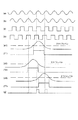
図6は、図5の信号処理回路部6によって、図25に示したような光検出器5からの入力が処理されている様子を示すタイムチャートである。図6において、横軸は時間を表し、一定速度の変位が生じているときの各信号の変化を示している。
【0096】
まず、位相分割回路105において、変位に伴い周期的に変化するアナログ位置信号(a),(b)を位相分割して2値化することによって、デジタル位置信号(c),(d)が得られる。
【0097】
また、2値化回路102において、原点検出用信号(e)を所定のスライスレベルで2値化することによってデジタル原点検出用信号(f)が得られる。そして、ラッチ回路106において、2値化回路102からのデジタル原点検出用信号(f)の立ち上がりを検出してラッチ信号(i)をハイレベルとする。
【0098】
そして、このラッチ信号(i)がハイレベルの領域において、原点信号については、次の2つの方法のうちから1つを選択することで得る。この場合、ラッチ信号(i)がハイレベルの領域においてというよりも、原点信号が検出されるまでハイレベルを保持してといった方が正確である。即ち、ラッチ回路106は、原点検出を位置信号(a),(d)に同期させるために、同期のタイミングまでラッチ信号(i)のレベルを保持するように機能している。これにより、元のデジタル原点検出用信号(f)が非検出状態になっても、確実に位置信号に同期させて原点を検出できる。また、ラッチ回路106でのラッチ信号(i)は、原点検出がなされてから、次回の原点検出がなされるまでには、クリアされている必要がある。
【0099】
そして、原点信号について、次の2つの方法のうちから1つを選択することで得る。
【0100】
1つ目は、同期回路103において、位置信号(a)の立ち上がりに同期させてハイレベルとし、位置信号(d)のレベル変化に同期させてローレベルとすることで、原点信号を得るものである。
【0101】
2つ目は、同期回路103において、デジタル原点検出用信号(f)を位置信号(a)の立ち下がりに同期させてハイレベルとし、位置信号(d)のレベル変化に同期させてローレベルとすることで、原点信号を得るものである。
【0102】
これら2つのうちの1つを選択して原点信号(g)または(h)として出力するが、この選択はスイッチ104により行う。
【0103】
ここで、位置信号(a),(b)と(c),(d)との組合せは90°の位相差を持つ。
【0104】
また、アナログ信号である位置信号(a),(b)と原点検出用信号(e)とは、デジタル信号である位置信号(c),(d)と原点検出用信号(f)とを作り出すことができるものであれば、それらがどのようなタイプの信号でも構わない。また、入力がデジタル信号のみで、アナログ信号を含まなくても構わない。
【0105】
そして、位置検出はデジタル位置信号(c),(d)を図示しないカウンタに入力することによって行う。この場合、原点信号(g)または(h)が発生したときときに、カウンタをリセットすることで、位置検出の原点出しが可能となる。
【0106】
[効果]
原点検出用信号の出力の仕方に応じて位置信号との同期位置を選択することが可能である。従って、信号ノイズやふらつき、さらには、光学式のエンコーダでは光源の安定性、発光・受光素子の温度特性とそのばらつき、個々のエンコーダの設計とのずれなどの不安定要素によって生じ得る原点検出位置のずれを少なくする同期位置を選択することが可能である。
【0107】
さらに、本実施の形態に特有の効果としては、原点検出用信号(e)をラッチ回路106で保持するため、デジタル原点検出用信号(f)の検出幅が狭く、検出状態で無くなった後でも位置信号との同期を取ることが可能である。従って、上記不安定要素による、図6に示す原点検出用信号(e)の出力レベルの変化や、図中左右方向へのシフト、スライスレベルの変化などに対しても許容度が向上する。
【0108】
そして、ラッチ信号(i)の立ち上がり位置をA相の同期位置よりほぼ180°位相が進んだ位置に設計・配置することができれば、±180°の余裕度が生じる。即ち、位置信号のピッチの±1/2倍の位置ずれ許容度がある。また、ラッチ信号(i)の立ち上がり位置とA相の同期位置の位相差の設定が困難な場合でも、同期位置の選択により、±90°以上の余裕度が生じる。従って、原点信号(g)または(h)を選択することによって、原点検出精度の劣化を抑え、安定した原点検出が可能となる。
【0109】
また、この実施の形態では、信号処理回路部6を除いて原点検出のための補助信号発生用部材などを設けていない。従って、安定した原点検出ができ、且つ、小型で安価なエンコーダを供給することが可能である。
【0110】
さらに、第2の実施の形態に挙げた検出方向の位置信号との限定機能を持つ同期方法をとることによって原点一定方向に変位がなされているときのみ、原点検出が可能とすることができる。これにより、可動部のバックラッシュの影響を受けにくくしたり、原点検出時に2重に原点検出をせずに済ませることにつながるなどの利点が生まれ、高精度で使い勝手のよい原点検出が可能となる。
【0111】
(第4の実施の形態)
[構成]
図7は、本発明の第4の実施の形態によるエンコーダの主要部の構成を示す図である。ただし、信号処理回路部を除き、位置信号と原点検出用信号が得られれば、特に、限定されない。
【0112】
図7に示すように、この第4の実施の形態による光学式のエンコーダは、LED等の発光部1と該発光部1からのビーム光を平行光にするための光学素子2とを組み合わせた光源部10と、該光源部10からの平行光が順次に照射されるインデックススケール3及びスケール4と、該スケール4から見て光源部10の反対側に配置された光検出器5と、該光検出器5からの信号を処理してエンコーダ信号として出力する信号処理回路部6からなる。
【0113】
このような構成において、インデックススケール3、スケール4、光検出器5のうち、位置検出用に用いられるのは、インデックススケール3に形成されているスリット3aと、スケール4に形成されているスリット4aと、光検出器5に形成されている光検出部5aとの組合せである。
【0114】
また、原点検出用に用いられるのはインデックススケール3に形成されているスリット3bと、スケール4に形成されているスリット4bと、光検出器5に形成されている光検出部5bとの組合せである。
【0115】
ステージやモータなどの位置検出を行う対象物において、光源部10と光検出器5との組合せは、可動部と固定部のどちらか一方に取り付けられる。
【0116】
また、スケール4は、可動部と固定部のどちらか他方に取り付けられる。
【0117】
そして、インデックススケール3と光検出器5とにおいて、原点検出用のスリット3bと光検出部5bとが、それぞれ、3個ずつ設けられている。これら3個の光検出部5bでの各検出信号は、3つとも同様の波形パターンを有し、位相差は、以下の式を満足する。
【0118】
位相差α=[位置信号の1周期]×(i+1/3) …(式1)
ただし、iは整数である。
【0119】
なお、本実施の形態では光学式のエンコーダを挙げているが、磁気式など他のタイプでもよい。
【0120】
図8は、本発明の第4の実施の形態に係るエンコーダの信号処理回路部6の構成を示すブロック図である。
【0121】
即ち、この信号処理回路部6は、アナログ位置信号(a),(b)をデジタル位置信号(c),(d)に変換するための2値化回路101と、原点検出用信号(e1),(e2),(e3)を所定のスライスレベルで2値化してデジタル原点検出用信号(f1),(f2),(f3)に変換する2値化回路102と、この2値化回路102からのデジタル原点検出用信号(f1),(f2),(f3)の内の1つを2値化回路101からのデジタル位置信号(c),(d)に同期させて原点信号(g)を発生させる同期回路103と、この同期回路103における同期のタイミングを切り替えるスイッチ104とからなる。
【0122】
なお、図8においては、デジタル位置信号(c),(d)に同期させて原点信号(g)を得ているが、アナログ位置信号(a),(b)に同期させて原点信号(g)を得ることも同様の機能で実現できる。
【0123】
また、後述するように、この実施の形態においては、位置信号(a)に同期させて原点信号(g)を検出する状態としているが、位置信号(b),(c),(d)に同期させても同様の機能で実現できる。
【0124】
[作用]
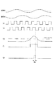
図9は、図8の信号処理回路部6によって、図7に示したような光検出器5からの入力が処理されている様子を示すタイムチャートである。図9において、横軸は時間を表し、一定速度の変位が生じている時の各信号の変化を示している。
【0125】
まず、2値化回路101において、変位に伴い周期的に変化するエンコーダのアナログ位置信号(a),(b)を2値化することによって、デジタル位置信号(c),(d)が得られる。
【0126】
また、2値化回路102において、原点検出用信号(e1),(e2),(e3)を所定のスライスレベルで2値化することによって、デジタル原点検出用信号(f1),(f2),(f3)が得られる。
【0127】
そして、同期回路103において、このデジタル原点検出用信号(f1),(f2),(f3)の内の1つをスイッチ104に応じて選択する。この場合、同期回路103においては、選択されたデジタル原点検出用信号が検出状態にあるときに位置信号(a)または(c)の立ち上がりに同期させてハイレベルとし、位置信号(b),(d)のレベル変化に同期させてローレベルとする原点信号(g)を生成する。なお、図9において、デジタル原点検出用信号(f1),(f2),(f3)に対応する原点信号(g)の検出状態部分はパルス状の部分の内、ぞれぞれ、実線の部分、細い点線の部分、点線の部分である。
【0128】
ここで、位置信号(a),(b)と、(c),(d)との組合せは90°の位相差を持つ。また、アナログ信号である位置信号(a),(b)と原点検出用信号(e1),(e2),(e3)は、デジタル信号である位置信号(c),(d)と原点検出用信号(f1),(f2),(f3)を作り出せれば、どのようなタイプの信号でも構わない。また、検出系からの入力がデジタル信号のみで、アナログ信号を含まなくても構わない。また、位置信号をデジタル化する際にはさらに位相分割により分解能を向上させたものとしても構わない。
【0129】
位置検出は、デジタル位置信号(c),(d)を図示しないカウンタに入力することで行う。そして、原点信号(g)が発生したときに、カウンタをリセットすることによって、位置検出の原点出しが可能となる。
【0130】
[効果]
複数の原点検出用信号の中から1つを選択することで位置信号との同期位置を選択することが可能である。
【0131】
従って信号ノイズやふらつき、さらには、光学式のエンコーダでは光源の安定性、発光・受光素子の温度特性とそのばらつき、個々のエンコーダの設計とのずれなどの不安定要素によって生じ得る原点検出位置のずれを少なくする同期位置を選択することが可能である。
【0132】
例えば、上記不安定要素により、図9に示す原点検出用信号(e1),(e2),(e3)の出力レベルが変化したり、図中左右方向にシフトしたり、スライスレベルが若干上下することが考えられる。このとき、原点検出用信号(e1)と(e3)を用いて発生する原点信号(g)は比較的安定であるが、原点検出用信号(e2)を用いる場合には、位置信号との同期位置に近いため、不安定になりやすい。この場合、得られる原点位置には1周期分、またはそれ以上、の差が出ることもあるが、常に、一方のみを使用すれば、実用上問題にはならない。
【0133】
なお、同期の仕方として、原点検出位置近傍での変位を計測しながら、原点検出用信号と位置信号の同期を取る方法も取られている。この場合には、両者の差が小さい原点検出用信号(e2)を用いるのが望ましく、この場合には最大±1周期分の検出位置ずれの許容度を持つ。
【0134】
従って、以上のような方法によって原点信号(g)を選択することによって原点検出精度の劣化を抑え、安定した原点検出が可能となる。
【0135】
(第5の実施の形態)
[構成]
図10は、本発明の第5の実施の形態に係るエンコーダの主要部の構成を示す図である。
【0136】
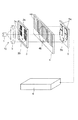
図10において、エンコーダは、大きく分けてベース21、面発光レーザ22、フォトIC23、スケール24の4つの部分からなる。
【0137】
ベース21、面発光レーザ22、フォトIC23は、本体として一体に構成され、スケール24に対してギャップdで適正な姿勢を保ったまま保持される。
【0138】
ベース21の上には、スケール24に対して斜めに配置されたビーム出射口22a及び出射口22bを持つ面発光レーザ22と、ピッチPpで同一構造の要素が並んだ受光アレイ部23a、受光部23bと信号処理回路23cからなるフォトIC23、が形成される。
【0139】
ビーム出射口22a及び出射口22bと面発光レーザ22とは、光源として半導体プロセスにより一体成形されている。
【0140】
この光源の波長は800nm乃至1000nm程度とし、受光アレイ部はシリコンベースの半導体とする。
【0141】
なお、波長の異なる光源を用いる場合には、その波長を検出するのに望ましい受光部を用いることによって対応が可能である。
【0142】
また、信号処理回路23cは、レーザ駆動回路、受光アレイ部23a及び受光部23bの信号のゲイン・オフセット調整をする正規化回路からなる。
【0143】
ここで、受光アレイ部23aの4つ置きのアレイ要素の信号の和の1つをA(+)信号、1つ隣の4つ置きのアレイ要素の信号の和をB(+)信号、さらに1つ隣の4つ置きのアレイ要素の信号の和をA(−)信号、残る4つ置きのアレイ要素の信号の和をB(−)信号とする。
【0144】
そして、[A(+)−A(−)]信号をA信号、[B(+)−B(−)]信号をB信号として、この2つのA信号、B信号をエンコーダ信号として出力するように、信号処理回路23cは構成されている。
【0145】
スケール24には、反射率の異なる2つのパターンを数10μmのピッチPsで並べた位置検出パターン24aがあり、その端部には原点検出用パターン24bが形成されている。
【0146】
ここで、上記受光アレイ部23aの各要素間のピッチPpと、この位置検出パターン24aのピッチPsには以下の関係がある。
【0147】
Pp=2Ps
そして、ビーム出射口22aから出射したレーザ光は広がりを持ってスケール24の位置検出パターン24aに入射し、該位置検出パターン24aによって回折されたレーザ光が受光アレイ部23aに入射するように構成されるとともに、配置されている。
【0148】
なお、レーザ光が平行光な場合には、回折像の結像条件を満たすように光源・スケール・受光部を配置すればよい。
【0149】
面発光レーザ22とフォトIC23の図10中のz方面の高さは等しくなるよう配置されている。
【0150】
ギャップdは、位置検出パターン24aの2倍の像が受光アレイ部23aに結像するように決められる。このギャップは、レーザ光の波長、出射角度によって解像度が高くなる範囲が決まる。
【0151】
なお、本実施の形態では、スケール面での反射による回折像を用いているが、透過光を利用し、受光部をスケールの図10中の上方に配置することも可能である。この場合の光源とスケール間ギャップ、スケールと受光部間のギャップは、波長、出射角度によって解像度が高くなるように選択し、2つのギャップの距離は必ずしも等しくなくてもよい。
【0152】
ただし、2つのギャップ量が異なるときには、スケールピッチと受光アレイ部のピッチには以下の関係が成り立つ。
【0153】
Ps:Pp=(光源・スケール間のギャップ量):(光源・スケール間のギャップ量+スケール・受光部間のギャップ量)
上記のように規定されたギャップに対して、原点検出用パターン24bが所定の位置にあるときにビーム出射口22bのレーザ光が原点検出用パターン24bによって回折され、受光部23bに集光するようにスケール24が設計されている。
【0154】
ここで、ベース21とスケール24とは、ギャップdが一定でスケール24のピッチ方向、即ち、図10中のx方向に相対移動可能なように配置されている。
【0155】
そして、面発光レーザ22のビーム出射間隔は、原点検出時の位置信号のA信号との位相差が、位置信号の1周期の1/2となるように設計されている。
【0156】
また、面発光レーザ22とフォトIC23とは共に半導体プロセスで作成されており、それらの加工精度は数μm以下である。
【0157】
図11は、本発明の第5の実施の形態に係るエンコーダの信号処理回路部(原点検出回路部)6の構成を示すブロック図である。
【0158】
この信号処理回路部(原点検出回路部)6は、アナログ位置信号A,Bを位相分割し、デジタル信号(c),(d)に変換するための位相分割回路105、原点検出用信号(e)を所定のスライスレベルで2値化してデジタル原点検出用信号(f)に変換する2値化回路102、デジタル原点検出用信号(f)を位置信号Aの立ち上がりに同期させて原点信号(g)を発生させる同期回路103とからなる。
【0159】
図11においては、信号Aの立ち上がりは、後述するように、振幅の中心をよぎる点で検出する。
【0160】
また、信号Aの立ち上がりに同期させて原点信号(g)を得ているが、位置信号A,B,(c),(d)の中から適切な信号を選択して同期させてもよい。
【0161】
[作用]
まず、エンコーダとしての位置検出機能を説明する。
【0162】
面発光レーザ22から出射したレーザ光はスケール24の位置検出パターン24aに入射し、この位置検出パターン24aによって反射されたレーザ光が受光アレイ部23aで検出される。
【0163】
そして、ベース21とスケール24が相対移動すると、受光アレイ部23aで検出される電気信号は三角波として強度が変化する。
【0164】
受光アレイ部23aで検出される2つの電気信号A,Bには1/4周期の位相差があるため、この2つの信号を用いて相対移動方向を含めてベース21とスケール24の相対移動の移動量を知ることができる。
【0165】
位置検出は、デジタル位置信号(c),(d)を図示しないカウンタに入力することによって行われる。
【0166】
次に、原点検出の手順を示す。
【0167】
図12は、図11の信号処理回路部(原点検出回路部)6によって、信号処理回路23c(受光アレイ部23a及び受光部23b)からの入力が処理されている様子を示すタイムチャートである。図12において、横軸は時間を表し、一定速度の変位が生じている時の各信号の変化を示している。
【0168】
まず、位相分割回路105において、変位に伴い周期的に変化するエンコーダのアナログ位置信号A,Bを位相分割し2値化することでデジタル位置信号(c),(d)が得られる。
【0169】
また、2値化回路102において、原点検出用信号(e)を所定のスライスレベルで2値化することでデジタル原点検出用信号(f)が得られる。
【0170】
そして、同期回路103において、信号Aの立ち上がりに同期させてハイレベルとし、位置信号(d)のレベル変化に同期させてローレベルとすることによって原点信号(g)が得られる。
【0171】
ここで、位置信号(c),(d)の組合せは90°の位相差を持つ。
【0172】
そして、原点信号(g)が発生したときに、原点信号(g)をカウントする図示しないカウンタをリセットすることによって、位置検出の原点出しが可能となる。
【0173】
[効果]
原点検出用信号と位置信号との位相差が、予め、設計により最適な値とすることが可能である。また、その誤差も半導体プロセスによる精度では数μm以下となる。従って、信号ノイズやふらつき、さらには、光学式のエンコーダでは光源の安定性・発光・受光素子の温度特性とそのばらつき、個々のエンコーダの設計とのずれなどの不安定要素によって生じ得る原点検出位置のずれを少なくすることが可能である。
【0174】
さらには、原点信号の同期を取る際に、組立・取付け時の許容度を大きくできる。例えば、上記不安定要素により、図12に示す原点検出用信号(e)の出力レベルが上がったり、図12中の左方向にシフトしたり、スライスレベルが若干下がることに対する許容度が大きくなり、原点検出精度の劣化を抑え、安定した原点検出が可能となる。
【0175】
また、この実施の形態では、信号処理回路部(原点検出回路部)6を除いて原点検出のための補助信号発生用部材などを設けていない。更に、他の実施の形態に比較しても、同期タイミングの切り替えスイッチなどを省略することができている。従って、安定した原点検出ができ、且つ、小型で安価なエンコーダを供給することが可能である。
【0176】
(第6の実施の形態)
この第6の実施の形態では、移動体の位置変位を検出するエンコーダであり、上記移動体の移動に応じて複数の周期信号を発生すると共に、上記移動体が所定の位置にある場合に、原点検出用信号を発生し、上記複数の周期信号から、1つの周期信号を選択可能であり、上記原点検出用信号に基づいて、上記選択された上記周期信号に同期して、上記移動体が原点位置にあることを検出することを特徴としている。
【0177】
[構成]
この第6の実施の形態に係るエンコーダにおける信号処理回路部の構成は、前述した第1の実施の形態における信号処理回路部の構成と、同様であるが、スイッチ104の機能が異なる。
【0178】
[作用]
図13は、この第6の実施の形態における信号処理回路部6によって、光検出器5からの入力が処理されている様子を示すタイムチャートである。同図において、位置信号(a),(b),(c),(d)及び原点検出用信号(e)とデジタル原点検出用信号(f)とは、図2と同様である。
【0179】
そして、原点信号(g)または(h)については、次に示すような2つの方法のうちから1つを選択することで得られる。
【0180】
1つ目は、デジタル原点検出用信号(f)の位置信号(c)の立ち下りに同期させてハイレベルとし、位置信号(d)のレベル変化に同期させてローレベルとすることで、原点信号(g)を得るものである。
【0181】
2つ目は、デジタル原点検出用信号(f)を位置信号(d)の立ち下りに同期させてハイレベルとし、位置信号(c)のレベル変化に同期させてローレベルとすることで、原点信号(h)を得るものである。
【0182】
このような原点信号(g)または(h)の選択は、スイッチ104で行う。
【0183】
原点検出用信号(e)のレベル変化によって、所定のスライスレベルによって原点検出用信号(e)を2値化したデジタル原点検出用信号(f)は、その位置と幅が変化する。このデジタル原点検出用信号(f)の変化によって、原点信号(g)は位置が変化するが、原点信号(h)は変化しない。
【0184】
[効果]
この第6の実施の形態によっても、前述した各実施の形態における効果と同様の効果が得られる。
【0185】
(第7の実施の形態)
[構成]
この第7の実施の形態の主要部の構成は、信号処理回路部6を除き、位置信号と原点検出用信号が得られるものであれば、特に、限定されない。例えば、前述した第1の実施の形態の主要部の構成として図25に示したような光学式のエンコーダ構成など一般的なものでよい。また、図25の例では光学式のエンコーダを挙げているが、磁気式など他のタイプでもよい。
【0186】
図14は、本発明の第7の実施の形態に係るエンコーダの信号処理回路部6の構成を示すブロック図である。
【0187】
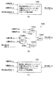
この第7の実施の形態による信号処理回路部6は、アナログ位置信号(a),(b)をデジタル位置信号(c),(d)に変換するための2値化回路101と、原点検出用信号(e)を所定のスライスレベルで2値化してデジタル原点検出用信号(f)に変換する2値化回路102と、この2値化回路102からのデジタル原点検出用信号(f)を2値化回路101からのデジタル位置信号(c),(d)に同期させて原点信号(g)または(h)を発生させる同期回路103と、この同期回路103における同期のタイミングを切り替えるスイッチ104と、最適同期位置を検知する判定回路107と、この判定回路107による最適同期位置判定結果を表示する表示器108とからなる。
【0188】
図15の(A)は上記同期回路103の構成例を示し、図15の(B)は上記判定回路107の構成例を示している。
【0189】
即ち、同期回路103は、位置信号(c)の立ち上がり検出部103gと立ち下がり検出部103h、これらの検出部103g,103hからの出力信号を上記スイッチ104の切り替えに応じて選択する選択スイッチ103i、この選択スイッチ103iで選択された検出部103g,103hの出力信号と原点検出用信号(f)との論理積を取るAND回路103jとから成る。
【0190】
また、判定回路107では、位置信号(d)と原点検出用信号(f)をD−Cトリガタイプのフリップフロップ(LS423など)107aのD(データ)及びCLK(クロック)へそれぞれ接続している。そして、原点検出用信号(f)を、このフリップフロップ107aでの信号遅延約10nsecを上回る遅延を持つ抵抗107bとコンデンサ107cの組合せに通し、この出力とフリップフロップ107aの出力Q及び
【数1】
![]()
【0191】
なお、図14においては、位置信号(c),(d)に同期させて原点信号(g)または(h)を得ているが、位置信号(a),(b)に同期させても同様の機能が実現できる。
【0192】
[作用]
図14の信号処理回路部6によって、図25に示したような光検出器5からの入力を処理する際のタイムチャートは、前述した第1の実施の形態における図2のそれと同様であるので、以下の説明は、図2を参照して行う。
【0193】
即ちまず、2値化回路101において、変位に伴い周期的に変化するエンコーダのアナログ位置信号(a),(b)を2値化することによって、デジタル位置信号(c),(d)が得られる。
【0194】
また、2値化回路102において、原点検出用信号(e)を所定のスライスレベルで2値化することによって、デジタル原点検出用信号(f)が得られる。
【0195】
そして、原点信号については、次の2つの方法のうちから1つを選択することで得られる。
【0196】
1つ目は、同期回路103において、デジタル原点検出用信号(f)を位置信号(a),(c)の立ち上がりに同期させてハイレベルとし、位置信号(b),(d)のレベル変化に同期させてローレベルとすることで、原点信号(g)を得るものである。ここで、上記位置信号(a),(c)の立ち上がりは立ち上がり検出部103gにより検出し、位置信号(b),(d)のレベル変化は図示しないレベル変化検出部(例えばローレベル検出回路)により検出することができる。
【0197】
2つ目は、同期回路103において、デジタル原点検出用信号(f)を位置信号(a),(c)の立ち下がりに同期させてハイレベルとし、位置信号(b),(d)のレベル変化に同期させてローレベルとすることで、原点信号(h)を得るものである。ここで、上記位置信号(a),(c)の立ち下がりは立ち下がり検出部103hにより検出し、位置信号(b),(d)のレベル変化は図示しないレベル変化検出部(例えばハイレベル検出回路)により検出することができる。
【0198】
これら2つのうちの1つを選択して原点信号(g)または(h)として出力するが、この選択はスイッチ104により行う。
【0199】
ここで、位置信号(a),(b)と(c),(d)の組合せは、90°の位相差を持つ。
【0200】
また、アナログ信号である位置信号(a),(b)と原点検出用信号(e)とは、デジタル信号である位置信号(c),(d)と原点検出用信号(f)を作り出すことができるものであれば、それらがどのようなタイプの信号でも構わない。また、図25に示したような光検出器5からの入力がデジタル信号のみで、アナログ信号を含まなくても構わない。また、入力されるアナログの位置信号をデジタル化する際には、さらに、位相分割により分解能を向上させたものとしても構わない。
【0201】
そして、位置検出は、デジタル位置信号(c),(d)を図示しないカウンタに入力することによって行う。この場合、原点信号(g)または(h)が発生したときに、カウンタをリセットすることによって、位置検出の原点出しが可能となる。
【0202】
一方、判定回路107では、原点検出用信号(f)を検知した時点での位置信号(c)の位相が、最も近い立ち上がり(位相0°とする)と立ち下がり(位相180°とする)の内、どちらに近いかを判定して、位相差の大きい方を安定と見なして出力する。この最適同期位置判定結果は、表示器108へ、または、電気信号として外部へ出力される。
【0203】
なお、表示器108は、結果が示せるものであれば、どのようなタイプの物でも良いが、例えば、立ち上がり及び立ち下がりの2つを示すLEDの内、最適な方を原点検出時に点灯するものや、2色点灯可能なLEDの表示色を切り替えるものとすることができる。
【0204】
ここで、具体的な判定方法を説明する。
【0205】
先ず、位置信号(c),(d)のレベルを確認する。図2の位置信号(c),(d)においては、位置信号(c)の方が位相が90°進んでいる。この状態において、位置信号(c)の立ち上がり時の位置信号(d)のレベルはローレベルである。このことから、位置信号(d)のレベルがローレベルの時は位置信号(c)の立ち上がりまでの位相差は±90°以内であり、位置信号(d)のレベルがハイレベルの時は位置信号(c)の立ち上がりまでの位相差は±90°以上である。
【0206】
従って、原点検出信号(f)の立ち上がり検出時の位置信号(d)のレベルがハイレベルであれば、位置信号(c)の立ち上がりに同期させた場合に、原点検出信号(f)の立ち上がり位置の若干の変動に対してローレベルの時に比べてより安定である。同様の議論により、原点検出信号(f)の立ち上がり検出時の位置信号(d)のレベルがローレベルであれば、位置信号(c)の立ち下がりに同期させた場合に、原点検出信号(f)の立ち上がり位置の若干の変動に対してハイレベルの時に比べてより安定である。従って、より安定な同期位置を判定結果として出力すればよい。
【0207】
例えば、図2中で、原点検出用信号(f)が検出された瞬間(立ち上がり時)の位置信号(d)のレベルは、図より、原点検出用信号(e)の太線(原点検出用信号(f)の実線)の例ではハイレベルである。従って、位置信号(c)の最も近い立ち上がりと立ち下がりに関して、立ち上がりの方が位相差が大きく安定であることが判り、立ち上がりの方を判定結果として出力する。
【0208】
[効果]
原点検出用信号の出力の仕方に応じて位置信号との同期位置を選択することが可能である。従って、信号ノイズやふらつき、更には、光学式のエンコーダでは光源の安定性、発光・受光素子の温度特性とそのばらつき、個々のエンコーダの設計とのずれなどの不安定要素によって生じ得る原点検出位置のずれを少なくする同期位置を選択することが可能である。
【0209】
例えば、上記不安定要素により、図2の原点検出用信号(e)の出力レベルが上がったり、図中左方向にシフトしたり、スライスレベルが若干下がることが考えられる。このとき、原点検出用信号(e)が太線から細線のように変化したとすると、デジタル原点検出用信号(f)は破線のようになる。これにより、原点信号(h)においては破線で示した1周期分ずれた位置が原点信号として検出される。これに対して、原点信号(g)ではこのような変化は起きにくい。従って、原点信号(g)を選択することで、原点検出精度の劣化を抑え、安定した原点検出が可能となる。
【0210】
そして、本実施の形態では、原点信号の位置信号への同期をとるに当たり、複数の同期位置の内、どれが最良かを判断する判定回路107を有しており、実際にエンコーダを装置に取り付けた状態で最良の同期位置を選ぶことができる。
【0211】
この場合、本実施の形態においては、位相余裕の大きい方の同期位置を選択することにより、変動などに対する安定性を向上させることが可能となっている。このことにより、位置信号に同期させた原点検出の安定性が増すと共に、エンコーダの取付け時のヘッドとスケールの取付け角度やギャップ等といった相対位置や姿勢のばらつきの影響を事前に考慮する必要が無くなる。即ち、位置信号と原点信号の位相差を厳密に設計や製作において設定して加工する必要がないため、製作コストや組立調整の時間短縮につながると共に、設計や製作上の制約が減ることによって機能上の自由度が上がり得る利点がある。
【0212】
また、本実施の形態においては、立ち上がりと立ち下がりのどちらを選ぶかの判定手段として原点検出用信号の他に2つの位置信号のみを処理する回路を用いており、その時の表示器108も2つのLED程度であり、追加することによる負担も軽い割に位置信号に同期させた原点検出の安定性が容易に実現できる。
【0213】
また、本実施の形態では、信号処理回路部6を除いて原点検出のための補助信号発生用部材などを設けていない。従って、安定した原点検出ができ、且つ、小型で安価なエンコーダを供給することが可能である。
【0214】
(第8の実施の形態)
[構成]
この第8の実施の形態の主要部の構成は、第7の実施の形態と同様に、信号処理回路部6を除き、位置信号と原点検出用信号が得られるものであれば、特に、限定されない。例えば、前述した第1の実施の形態の主要部の構成として図25に示したような光学式のエンコーダ構成など一般的なものでよい。また、図25の例では光学式のエンコーダを挙げているが、磁気式など他のタイプでもよい。
【0215】
また、本発明の第8の実施の形態における信号処理回路部6の構成については、図14に示したブロック図と同様のものでよい。但し、信号処理回路部6における同期回路103及び判定回路107については、以下のような構成のものとする。
【0216】
図16の(A)乃至(C)は同期回路103の構成を示す図であり、図16の(A)に示す回路と図16の(C)に示す回路とがスイッチ104により切り替えられるようになっている。これらの回路は一般に入手可能なロジックICなどで容易、且つ、安価に製作が可能である。また、図16の(B)は、図16の(A)の回路の具体的な構成を示す図である。
【0217】
90°位相差の有る位置信号は、検出方向が変わると位相の進み方が逆転する。このことを利用して、方向判別が可能である。即ち、位置信号(c)が立ち上がりの時に検出方向(ステージ移動方向)によって位置信号(d)がローとなったり、ハイとなったりする。従って、位置信号(d)のレベルを規定することで方向判別が可能となる。そこで、図16の(A)に示す検出回路103kにおいて、位置信号(c)の立ち上がりに同期を取ると共に、位置信号(d)がローレベルとなる時に検出を限定することで、原点検出の方向を限定している。
【0218】
また、同一の検出方向で位置信号(c)の立ち下がりに同期させた同期回路103の構成を図16の(C)に示している。即ち、図16の(A)の検出回路103kで検出する位置信号(c)が立ち上がりの時で位置信号(d)がローレベルとなる時におけるステージ移動方向と、図16の(C)の検出回路103lで検出する位置信号(c)が立ち下がりの時で位置信号(d)がハイレベルとなる時におけるステージ移動方向とは、同一方向であり、原点検出の際の位相を180°ずらすことをスイッチ104で切り替えることを目的としている。
【0219】
図17は、本第8の実施の形態における判定回路107の構成例を示す図で、上記第7の実施の形態における図15の(B)の構成に方向判別のためのD−Cトリガタイプのフリップフロップ107fを追加したものである。
【0220】
即ち、方向判別のためのフリップフロップ107fには、データDとして位置信号(c)を、クロックCLKとして位置信号(d)を入力する。最適位置判別のためのフリップフロップ107aには、データDとして位置信号(d)を、クロックCLKとして原点検出信号(f)を入力する。そして、フリップフロップ107fのQ出力とフリップフロップ107aのQ出力と原点検出信号(f)の3つが全てハイレベルの時、AND回路107dの出力である判定1がハイレベルとなる。同様に、フリップフロップ107fのQバー出力とフリップフロップ107aのQバー出力と原点検出信号(f)の3つが全てハイレベルの時、判定2がハイレベルとなるようにAND回路107eで論理積が取られている。
【0221】
[作用]
本実施の形態における信号処理回路部6によって、図25に示したような光検出器5からの入力を処理する際のタイムチャートは、前述した第1の実施の形態における図2のそれと同様であるので、以下の説明は、図2を参照して行う。
【0222】
即ち、まず、2値化回路101において、変位に伴い周期的に変化するエンコーダのアナログ位置信号(a),(b)を2値化することによって、デジタル位置信号(c),(d)が得られる。
【0223】
また、2値化回路102において、原点検出用信号(e)を所定のスライスレベルで2値化することによって、デジタル原点検出用信号(f)が得られる。
【0224】
そして、原点信号については、次の2つの方法のうちから1つを選択することで得られる。
【0225】
1つ目は、同期回路103の検出回路103kにおいて、デジタル原点検出用信号(f)を位置信号(a),(c)の立ち上がりに同期させてハイレベルとし、位置信号(b),(d)のレベル変化に同期させてローレベルとすることで、原点信号(g)を得るものである。
【0226】
2つ目は、同期回路103の検出回路103lにおいて、デジタル原点検出用信号(f)を位置信号(a),(c)の立ち下がりに同期させてハイレベルとし、位置信号(b),(d)のレベル変化に同期させてローレベルとすることで、原点信号(h)を得るものである。
【0227】
これら2つのうちの1つを選択して原点信号(g)または(h)として出力するが、この選択はスイッチ104により行う。
【0228】
ここで、原点信号(g)について、図16の(B)に基づき、より詳細に説明する。
【0229】
まず、方向判別について説明する。フリップフロップ103k1のデータDへは位置信号(d)を、クロックCLKへは位置信号(c)を入力する。この結果、フリップフロップ103k1のQバー出力から出力される信号は、位置信号(c)の立ち上がりの度に位置信号(d)の反転信号として更新される。そのため、位置信号(c)の立ち上がり時に位置信号(d)がローレベルの時のみフリップフロップ103k1のQバー出力がハイレベルとなるため、方向判別が可能となる。
【0230】
そして、AND回路103k2により、このような検出方向判別信号と原点検出信号(f)の論理積を取ることで、検出方向が正しく、原点検出信号(f)が検知状態である場合に限定する。
【0231】
また、更に原点信号を出すための条件を追加する。即ち、本実施の形態では、位置信号(c)の立ち上がりから位置信号(d)の立ち上がりまでを検出する。位置信号(c)の立ち上がりエッジが重要な点であり、検出幅については時間で指定したり、測定対象物の変位量で指定してもよく、幅そのものも任意に指定して構わない。方向が指定された上で、位置信号(c)の立ち上がりから位置信号(d)の立ち上がりまでという場合、位置信号(c)がハイレベルで位置信号(d)がローレベルであることと等価である。従って、この条件を付加する。
【0232】
つまり、以上のことから、原点信号(g)は、位置信号(c)がハイレベルであること、位置信号(d)がローレベルであること、方向判別として位置信号(c)の立ち上がり時に位置信号(d)がローレベルであること、原点検出信号(f)がハイレベル(検知状態)であること、の4つの論理積を取ることで、得られる。即ち、位置信号(c)とNOT回路103k3で反転した位置信号(d)との論理積をAND回路103k4で取り、このAND回路103k4の出力と上記AND回路103k2の出力との論理積をAND回路103k5で取ることで、原点信号(g)を得る。
【0233】
なお、位置信号(a),(b)と(c),(d)の組合せは、90°の位相差を持つ。また、アナログ信号である位置信号(a),(b)と原点検出用信号(e)とは、デジタル信号である位置信号(c),(d)と原点検出用信号(f)を作り出すことができるものであれば、それらがどのようなタイプの信号でも構わない。また、図25に示したような光検出器5からの入力がデジタル信号のみで、アナログ信号を含まなくても構わない。また、入力されるアナログの位置信号をデジタル化する際には、さらに、位相分割により分解能を向上させたものとしても構わない。
【0234】
そして、位置検出は、デジタル位置信号(c),(d)を図示しないカウンタに入力することによって行う。この場合、原点信号(g)または(h)が発生したときに、カウンタをリセットすることによって、位置検出の原点出しが可能となる。
【0235】
なお、図4は、図2とは逆方向に変位が生じた際の各信号の変化を示している。この時、アナログ位置信号(a),(b)及びデジタル位置信号(c),(d)の位相の進みは逆転している。
【0236】
このように逆方向に変位が生じるとき、同期回路103は、図16の(A)(及び(C))に示すような構成及びその作用により、原点信号(g)及び(h)を検出状態としない。従って、逆方向の変位では原点検出はなされない。なお、図16の(A)乃至(C)に示す同期回路103を適切に設計することにより、逆方向の変位でのみ原点検出を可能とすることもできる。
【0237】
一方、判定回路107では、原点検出用信号(f)を検知した時点での位置信号(c)の位相が、最も近い立ち上がり(位相0°とする)と立ち下がり(位相180°とする)の内、どちらに近いかを判定して、位相差の大きい方を安定と見なして出力する。この最適同期位置判定結果は、表示器108へ、または、電気信号として外部へ出力される。
【0238】
なお、表示器108は、結果が示せるものであれば、どのようなタイプの物でも良いが、例えば、立ち上がり及び立ち下がりの2つを示すLEDの内、最適な方を原点検出時に点灯するものや、2色点灯可能なLEDの表示色を切り替えるものとすることができる。
【0239】
ここで、具体的な判定方法を説明する。
【0240】
先ず、位置信号(c),(d)のレベルを確認する。図2の位置信号(c),(d)においては、位置信号(c)の方が位相が90°進んでいる。この状態において、位置信号(c)の立ち上がり時の位置信号(d)のレベルはローレベルである。このことから、位置信号(d)のレベルがローレベルの時は位置信号(c)の立ち上がりまでの位相差は±90°以内であり、位置信号(d)のレベルがハイレベルの時は位置信号(c)の立ち上がりまでの位相差は±90°以上である。
【0241】
従って、原点検出信号(f)の立ち上がり検出時の位置信号(d)のレベルがローレベルであれば、位置信号(c)の立ち上がりに同期させた場合に、原点検出信号(f)の立ち上がり位置の若干の変動に対してハイレベルの時に比べてより安定である。同様の議論により、原点検出信号(f)の立ち上がり検出時の位置信号(d)のレベルがハイレベルであれば、位置信号(c)の立ち下がりに同期させた場合に、原点検出信号(f)の立ち上がり位置の若干の変動に対してローレベルの時に比べてより安定である。従って、より安定な同期位置を判定結果として出力すればよい。
【0242】
例えば、図2中で、原点検出用信号(f)が検出された瞬間(立ち上がり時)の位置信号(d)のレベルは、同図の原点検出用信号(e),(f)の例ではハイレベルである。従って、位置信号(c)の最も近い立ち上がりと立ち下がりに関して、立ち下がりの方が位相差が大きく安定であることが判り、立ち下がりの方を判定結果として出力する。
【0243】
このような判定方法を具体的な回路として示したのが図17である。
【0244】
即ち、フリップフロップ107fにて位置信号(c)と位置信号(d)を用いて方向判別を行い、位置信号(d)の立ち上がり時に位置信号(c)がハイレベルの時のみ判定結果を出力する。ここで、位置信号(d)の立ち上がり時に位置信号(c)がハイレベルであることは、位置信号(c)の立ち上がり時に位置信号(d)がローレベルであることと検出方向の点に関して等価である。
【0245】
検出方向が指定の向きにおいて、原点検出用信号(f)の立ち上がり時の位置信号(d)のレベルがハイレベルの時に判定1、位置信号(d)のレベルがローレベルの時に判定2を結果として出力する。判定1は原点信号を位置信号(c)の立ち下がりに同期することを推奨するものであり、判定2は原点信号を位置信号(c)の立ち上がりに同期することを推奨するものである。
【0246】
[効果]
原点検出用信号の出力の仕方に応じて位置信号との同期位置を選択することが可能である。従って、信号ノイズやふらつき、更には、光学式のエンコーダでは光源の安定性、発光・受光素子の温度特性とそのばらつき、個々のエンコーダの設計とのずれなどの不安定要素によって生じ得る原点検出位置のずれを少なくする同期位置を選択することが可能である。
【0247】
例えば、上記不安定要素により、図2の原点検出用信号(e)の出力レベルが上がったり、図中左方向にシフトしたり、スライスレベルが若干下がることが考えられる。このとき、原点検出用信号(e)が太線から細線のように変化したとすると、デジタル原点検出用信号(f)は破線のようになる。これにより、原点信号(h)においては破線で示した1周期分ずれた位置が原点信号として検出される。これに対して、原点信号(g)ではこのような変化は起きにくい。従って、原点信号(g)を選択することで、原点検出精度の劣化を抑え、安定した原点検出が可能となる。
【0248】
また、原点信号の位置信号への同期をとるに当たり、複数の同期位置の内、どれが最良かを判断する判定回路107を有しており、実際にエンコーダを装置に取り付けた状態で最良の同期位置を選ぶことができる。本実施の形態においては、位相余裕の大きい方の同期位置を選択することにより、変動などに対する安定性を向上させることが可能となっている。このことにより、位置信号に同期させた原点検出の安定性が増すと共に、エンコーダの取付け時のヘッドとスケールの取付け角度やギャップ等といった相対位置や姿勢のばらつきの影響を事前に考慮する必要が無くなる。即ち、位置信号と原点信号の位相差を厳密に設計や製作において設定して加工する必要がないため、製作コストや組立調整の時間短縮につながると共に、設計や製作上の制約が減ることによって機能上の自由度が上がり得る利点がある。
【0249】
また、本実施の形態においては、立ち上がりと立ち下がりのどちらを選ぶかの判定手段として原点検出用信号の他に2つの位置信号のみを処理する回路を用いており、その時の表示器108も2つのLED程度であり、追加することによる負担も軽い割に位置信号に同期させた原点検出の安定性が容易に実現できる。
【0250】
また、本実施の形態では、信号処理回路部6を除いて原点検出のための補助信号発生用部材などを設けていない。従って、安定した原点検出ができ、且つ、小型で安価なエンコーダを供給することが可能である。
【0251】
更に、本第8の実施の形態特有の効果としては、一定方向に変位がなされているときのみ原点検出が可能なことが挙げられる。これにより、可動部のバックラッシュの影響を受けにくくしたり、原点検出時に2重に原点検出をせずに済ませることにつながるなどの利点が生まれ、高精度で使い勝手のよい原点検出が可能となる。
【0252】
(第9の実施の形態)
[構成]
本発明の第9の実施の形態は、前述した第3の実施の形態に上記第7の実施の形態のような最適同期位置の判定手段を付加したものである。
【0253】
この第9の実施の形態の主要部の構成は、第7の実施の形態と同様に、信号処理回路部6を除き、位置信号と原点検出用信号が得られるものであれば、特に、限定されない。例えば、前述した第1の実施の形態の主要部の構成として図25に示したような光学式のエンコーダ構成など一般的なものでよい。また、図25の例では光学式のエンコーダを挙げているが、磁気式など他のタイプでもよい。
【0254】
図18は、本発明の第9の実施の形態に係るエンコーダの信号処理回路部6の構成を示すブロック図である。
【0255】
この第9の実施の形態による信号処理回路部6は、アナログ位置信号(a),(b)を位相分割し、デジタル位置信号(c),(d)に変換するための位相分割回路105と、原点検出用信号(e)を所定のスライスレベルで2値化してデジタル原点検出用信号(f)に変換する2値化回路102と、デジタル原点検出用信号(f)の立ち上がりを保持してラッチ信号(i)とするラッチ回路106と、該ラッチ回路106からのラッチ信号(i)を位置信号(a),(d)に同期させて原点信号(g)または(h)を発生させる同期回路103と、該同期回路103における同期のタイミングを切り替えるスイッチ104と、最適同期位置を検知する判定回路107と、この判定回路107による最適同期位置判定結果を表示する表示器108とからなる。
【0256】
図18のような構成の信号処理回路部6においては、位置信号(a)の立ち上がり・立ち下がりは振幅の中心をよぎる点で検出する。また、位置信号(a),(d)に同期させて原点信号(g)または(h)を得ているが、位置信号(a),(b),(c),(d)の中から適切な信号を選択して同期させるようにしてもよい。
【0257】
[作用]
図18の信号処理回路部6によって、図25に示したような光検出器5からの入力を処理する際のタイムチャートは、前述した第3の実施の形態における図6のそれと同様であるので、以下の説明は、図6を参照して行う。
【0258】
即ちまず、位相分割回路105において、変位に伴い周期的に変化するアナログ位置信号(a),(b)を位相分割して2値化することによって、デジタル位置信号(c),(d)が得られる。
【0259】
また、2値化回路102において、原点検出用信号(e)を所定のスライスレベルで2値化することによってデジタル原点検出用信号(f)が得られる。そして、ラッチ回路106において、2値化回路102からのデジタル原点検出用信号(f)の立ち上がりを検出してラッチ信号(i)をハイレベルとする。
【0260】
そして、原点信号について、次の2つの方法のうちから1つを選択することで得る。
【0261】
1つ目は、同期回路103において、位置信号(a)の立ち上がりに同期させてハイレベルとし、位置信号(d)のレベル変化に同期させてローレベルとすることで、原点信号を得るものである。
【0262】
2つ目は、同期回路103において、デジタル原点検出用信号(f)を位置信号(c)の立ち下がりに同期させてハイレベルとし、位置信号(d)のレベル変化に同期させてローレベルとすることで、原点信号を得るものである。
【0263】
これら2つのうちの1つを選択して原点信号(g)または(h)として出力するが、この選択はスイッチ104により行う。
【0264】
なお、位置信号(a),(b)と(c),(d)との組合せは90°の位相差を持つ。また、アナログ信号である位置信号(a),(b)と原点検出用信号(e)とは、デジタル信号である位置信号(c),(d)と原点検出用信号(f)とを作り出すことができるものであれば、それらがどのようなタイプの信号でも構わない。また、入力がデジタル信号のみで、アナログ信号を含まなくても構わない。
【0265】
そして、位置検出はデジタル位置信号(c),(d)を図示しないカウンタに入力することによって行う。この場合、原点信号(g)または(h)が発生したときときに、カウンタをリセットすることで、位置検出の原点出しが可能となる。
【0266】
一方、判定回路107では、原点検出用信号(f)を検知した時点での位置信号(c)の位相が、最も近い立ち上がり(位相0°とする)と立ち下がり(位相180°とする)の内、どちらに近いかを判定して、位相差の大きい方を安定と見なして出力する。この最適同期位置判定結果は、表示器108へ、または、電気信号として外部へ出力される。
【0267】
なお、表示器108は、結果が示せるものであれば、どのようなタイプの物でも良いが、例えば、立ち上がり及び立ち下がりの2つを示すLEDの内、最適な方を原点検出時に点灯するものや、2色点灯可能なLEDの表示色を切り替えるものとすることができる。
【0268】
ここで、具体的な判定方法を説明する。
【0269】
先ず、位置信号(c),(d)のレベルを確認する。図6の位置信号(c),(d)においては、位置信号(c)の方が位相が90°進んでいる。この状態において、位置信号(c)の立ち上がり時の位置信号(d)のレベルはローレベルである。このことから、原点検出用(f)信号を検知した時点で位置信号(d)のレベルがローレベルの時は位置信号(c)の立ち上がりまでの位相差は±90°以内であり、位置信号(d)のレベルがハイレベルの時は位置信号(c)の立ち上がりまでの位相差は±90°以上である。
【0270】
従って、原点検出信号(f)の立ち上がり検出時の位置信号(d)のレベルがハイレベルであれば、位置信号(c)の立ち上がりに同期させた場合に、原点検出信号(f)の立ち上がり位置の若干の変動に対して立ち下がりに同期させた場合に比べてより安定である。同様の議論により、原点検出信号(f)の立ち上がり検出時の位置信号(d)のレベルがローレベルであれば、位置信号(c)の立ち下がりに同期させた場合に、原点検出信号(f)の立ち上がり位置の若干の変動に対して立ち上がりに同期させた場合に比べてより安定である。従って、より安定な同期位置を判定結果として出力すればよい。
【0271】
例えば、図6中で、原点検出用信号(f)が検出された瞬間(立ち上がり時)の位置信号(d)のレベルは、同図のような原点検出用信号(e),(f)の例ではハイレベルである。従って、位置信号(c)の最も近い立ち上がりと立ち下がりに関して、立ち上がりの方が位相差が大きく安定であることが判り、立ち上がりの方を判定結果として出力する。
【0272】
[効果]
原点検出用信号の出力の仕方に応じて位置信号との同期位置を選択することが可能である。従って、信号ノイズやふらつき、更には、光学式のエンコーダでは光源の安定性、発光・受光素子の温度特性とそのばらつき、個々のエンコーダの設計とのずれなどの不安定要素によって生じ得る原点検出位置のずれを少なくする同期位置を選択することが可能である。
【0273】
更に、本第9の実施の形態特有の効果としては、原点検出用信号(e)をラッチ回路106で保持するため、デジタル原点検出用信号(f)の検出幅が狭く、検出状態で無くなった後でも位置信号との同期を取ることが可能である。従って、上記不安定要素による、図6の原点検出用信号(e)の出力レベルの変化や、図中左右方向へのシフト、スライスレベルの変化などに対しても許容度が向上する。
【0274】
そして、ラッチ信号(i)の立ち上がり位置を位置信号(c)の同期位置よりほぼ180°位相が進んだ位置に設計・配置することができれば、±180°の余裕度が生じる。即ち、位置信号のピッチの±1/2倍の位置ずれ許容度がある。また、ラッチ信号(i)の立ち上がり位置とA相の同期位置の位相差の設定が困難な場合でも、同期位置の選択により、±90°以上の余裕度が生じる。従って、原点信号(g)または(h)を選択することによって、原点検出精度の劣化を抑え、安定した原点検出が可能となる。
【0275】
更に、本実施の形態では、原点信号の位置信号への同期をとるに当たり、複数の同期位置の内、どれが最良かを判断する判定回路107を有しており、実際にエンコーダを装置に取り付けた状態で最良の同期位置を選ぶことができる。
【0276】
この場合、本実施の形態においては、位相余裕の大きい方の同期位置を選択することにより、変動などに対する安定性を向上させることが可能となっている。このことにより、位置信号に同期させた原点検出の安定性が増すと共に、エンコーダの取付け時のヘッドとスケールの取付け角度やギャップ等といった相対位置や姿勢のばらつきの影響を事前に考慮する必要が無くなる。即ち、位置信号と原点信号の位相差を厳密に設計や製作において設定して加工する必要がないため、製作コストや組立調整の時間短縮につながると共に、設計や製作上の制約が減ることによって機能上の自由度が上がり得る利点がある。
【0277】
また、本実施の形態においては、立ち上がりと立ち下がりのどちらを選ぶかの判定手段として原点検出用信号の他に2つの位置信号のみを処理する回路を用いており、その時の表示器108も2つのLED程度であり、追加することによる負担も軽い割に位置信号に同期させた原点検出の安定性が容易に実現できる。
【0278】
また、本実施の形態では、信号処理回路部6を除いて原点検出のための補助信号発生用部材などを設けていない。従って、安定した原点検出がリアルタイムにでき、且つ、小型で安価なエンコーダを供給することが可能である。
【0279】
更に、上記第8の実施の形態で説明したような検出方向の位置信号との限定機能を持つ同期方法をとるようにすれば、一定方向に変位がなされているときのみ原点検出が可能とすることができる。これにより、可動部のバックラッシュの影響を受けにくくしたり、原点検出時に2重に原点検出をせずに済ませることにつながるなどの利点が生まれ、高精度で使い勝手のよい原点検出が可能となる。
【0280】
(第10の実施の形態)
[構成]
本発明の第10の実施の形態は、前述した第4の実施の形態に上記第7の実施の形態のような最適同期位置の判定手段を付加したものである。
【0281】
本実施の形態に係るエンコーダの主要構成は、図7に示したような、前述の第4の実施の形態におけるものと同様であるので、その説明は省略する。
【0282】
図19は、本第10の実施の形態に係るエンコーダの信号処理回路部6の構成を示すブロック図である。
【0283】
即ち、この信号処理回路部6は、アナログ位置信号(a),(b)をデジタル位置信号(c),(d)に変換するための2値化回路101と、原点検出用信号(e1),(e2),(e3)を所定のスライスレベルで2値化してデジタル原点検出用信号(f1),(f2),(f3)に変換する2値化回路102と、この2値化回路102からのデジタル原点検出用信号(f1),(f2),(f3)の内の1つを2値化回路101からのデジタル位置信号(c),(d)に同期させて原点信号(g)を発生させる同期回路103と、この同期回路103における同期のタイミングを切り替えるスイッチ104と、最適同期位置を検知する判定回路107と、この判定回路107による最適同期位置判定結果を表示する表示器108とからなる。
【0284】
なお、図19においては、位置信号(a)に同期させて原点信号(g)を検出する状態としているが、位置信号(b),(c),(d)に同期させても同様の機能で実現できる。
【0285】
[作用]
図19の信号処理回路部6によって、図7に示したような光検出器5からの入力を処理する際のタイムチャートは、前述した第4の実施の形態における図9のそれと同様であるので、以下の説明は、図9を参照して行う。
【0286】
まず、2値化回路101において、変位に伴い周期的に変化するエンコーダのアナログ位置信号(a),(b)を2値化することによって、デジタル位置信号(c),(d)が得られる。
【0287】
また、2値化回路102において、原点検出用信号(e1),(e2),(e3)を所定のスライスレベルで2値化することによって、デジタル原点検出用信号(f1),(f2),(f3)が得られる。
【0288】
そして、同期回路103において、このデジタル原点検出用信号(f1),(f2),(f3)の内の1つをスイッチ104に応じて選択する。この場合、同期回路103においては、選択されたデジタル原点検出用信号が検出状態にあるときに位置信号(a)または(c)の立ち上がりに同期させてハイレベルとし、位置信号(b),(d)のレベル変化に同期させてローレベルとする原点信号(g)を生成する。なお、図9において、デジタル原点検出用信号(f1),(f2),(f3)に対応する原点信号(g)の検出状態部分はパルス状の部分の内、ぞれぞれ、実線の部分、細い点線の部分、点線の部分である。
【0289】
ここで、位置信号(a),(b)と、(c),(d)との組合せは90°の位相差を持つ。また、アナログ信号である位置信号(a),(b)と原点検出用信号(e1),(e2),(e3)は、デジタル信号である位置信号(c),(d)と原点検出用信号(f1),(f2),(f3)を作り出せれば、どのようなタイプの信号でも構わない。また、検出系からの入力がデジタル信号のみで、アナログ信号を含まなくても構わない。また、位置信号をデジタル化する際にはさらに位相分割により分解能を向上させたものとしても構わない。
【0290】
位置検出は、デジタル位置信号(c),(d)を図示しないカウンタに入力することで行う。そして、原点信号(g)が発生したときに、カウンタをリセットすることによって、位置検出の原点出しが可能となる。
【0291】
一方、判定回路107では、原点検出用信号(f1),(f2),(f3)を検知した時点での位置信号(c)の最も近い立ち上がりに対して最も位相差の大きい、即ち、位相余裕のある原点検出用信号を安定と見なして出力する。この最適同期位置判定結果は、表示器108へ、または、電気信号として外部へ出力される。
【0292】
なお、表示器108は、結果が示せるものであれば、どのようなタイプの物でも良いが、例えば、各原点検出用信号を表す3つLEDの内、最適なものを原点検出時に点灯するものや、3色点灯可能なLEDの表示色を切り替えるものとすることができる。なお、2つ安定な選択肢があると判断した場合には、必ずしも1つに絞らずに同時に2つを表示しても構わない。
【0293】
ここで、具体的な判定方法を説明する。
【0294】
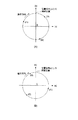
図9の位置信号(a),(b),(c),(d)においては、位置信号(b),(d)の方が位置信号(a),(c)に対して位相が90°進んでいる。これらを、図20の(A)及び(B)を用いて説明する。図9の位置信号(a),(b)の信号レベルの組合せを2次元のグラフに表すと図20の(A)及び(B)の円周上を右回りに動くことになる。ここで、位置信号(a)のレベルがマイナスからプラスになる、即ち、位置信号(c)の立ち上がりは、図20の(A)及び(B)中矢印で示した縦軸と円の交点の内、位置信号(b)がプラス側である上方の点となる。この点から最も遠い原点検出用信号検出時の位置が、系の変動に対して最も安定と言える。図20の(A)及び(B)中の(f1),(f2),(f3)の3点は、原点検出用信号(f1),(f2),(f3)が検出された瞬間の位置信号(a),(b)の位置を示している。
【0295】
原点検出用信号が検出された際の位置信号(d)のレベルがローレベル、即ち、原点検出用信号検出時の位置が円周上で下半分に存在すれば、少なくとも位相余裕が90°以上有り、安定である。各原点検出用信号の位相差は、既知であり、ほぼ120°である。従って、原点検出用信号が検出された際の位置信号(d)のレベルがローレベルになる原点検出用信号は1つ、または、2つである。
【0296】
図20の(A)の例のように、条件を満たす原点検出用信号が1つならば、それを最適な検出信号と判定すれば良い。
【0297】
これに対して、図20の(B)の例のように、条件を満たす原点検出用信号が2つならば、両方を安定と見なしても良い。
【0298】
ここで、2つの中からさらに1つに絞るのであれば、以下のようにする。即ち、図20の(B)の例では、位置信号(d)のレベルがハイレベルになる原点検出用信号が(f2)唯1つとなる。各原点検出用信号の位相差は既知でほぼ120°であるから、対応する点(f2)での位置信号(a)(即ち位置信号(c))のレベル(ローレベル)と逆のレベル(ハイレベル)を持つ点(f1)に対応する原点検出用信号(f1)が最も安定な原点検出用信号として判定できる。
【0299】
[効果]
本実施の形態によれば、複数の原点検出用信号の中から1つを選択することで、位置信号との同期位置を選択することが可能である。従って、信号ノイズやふらつき、更には、光学式のエンコーダでは光源の安定性、発光・受光素子の温度特性とそのばらつき、個々のエンコーダの設計とのずれなどの不安定要素によって生じ得る原点検出位置のずれを少なくする同期位置を選択することが可能である。
【0300】
例えば、上記不安定要素により、図9の原点検出用信号(e1),(e2),(e3)の出力レベルが変化したり、図中左右方向にシフトしたり、スライスレベルが若干上下することが考えられる。このとき、原点検出用信号(e1)と(e3)を用いて発生する原点信号(g)は比較的安定であるが、原点検出用信号(e2)を用いる場合には、位置信号との同期位置に近いため、不安定になりやすい。この場合、得られる原点位置には1周期分の差が出ることもあるが、常に一方のみを使用すれば、実用上問題にはならない。
【0301】
なお、同期の仕方として、原点検出位置近傍での変位を計測しながら、原点検出用信号と位置信号の同期を取る方法も取られている。この場合には、両者の差が小さい原点検出用信号(e2)を用いるのが望ましく、この場合には最大±1周期分の検出位置ずれの許容度を持つ。
【0302】
従って、以上のような方法によって原点信号(g)を選択することによって、原点検出精度の劣化を抑え、安定した原点検出が可能となる。
【0303】
さらに、本実施の形態では、原点信号の位置信号への同期をとるに当たり、複数の原点検出用信号の内、どれが最良かを判断する判定回路107を有しており、実際にエンコーダを装置に取り付けた状態で最良の同期位置を選ぶことができる。
【0304】
この場合、本実施の形態においては、位相余裕の大きい方の同期位置を選択することにより、変動などに対する安定性を向上させることが可能となっている。このことにより、位置信号に同期させた原点検出の安定性が増すと共に、エンコーダの取付け時のヘッドとスケールの取付け角度やギャップ等といった相対位置や姿勢のばらつきの影響を事前に考慮する必要が無くなる。即ち、位置信号と原点信号の位相差を厳密に設計や製作において設定して加工する必要がないため、製作コストや組立調整の時間短縮につながると共に、設計や製作上の制約が減ることによって機能上の自由度が上がり得る利点がある。
【0305】
また、本実施の形態においては、3つの原点出用信号のどれを選ぶかの判定手段として原点検出用信号の他に2つの位置信号のみを処理する回路を用いており、その時の表示器108も3つのLED程度であり、追加することによる負担も軽い割に位置信号に同期させた原点検出の安定性が容易に実現できる。
【0306】
(第11の実施の形態)
[構成]
次に、本発明の第11の実施の形態を説明する。
【0307】
本実施の形態に係るエンコーダの主要構成は、前述の第8の実施の形態と同様に、信号処理回路部6を除き、位置信号と原点検出用信号が得られれば、特に、限定されない。例えば、前述した第1の実施の形態の主要部の構成として図25に示したような光学式のエンコーダ構成など一般的なものでよい。また、図25の例では光学式のエンコーダを挙げているが、磁気式など他のタイプでもよい。
【0308】
また、本第11の実施の形態における信号処理回路6の構成については、図21に示すようになっている。
【0309】
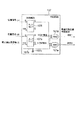
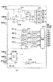
即ち、この第11の実施の形態による信号処理回路部6は、アナログ位置信号(a),(b)をデジタル位置信号(c),(d)に変換するための2値化回路101と、原点検出用信号(e)を所定のスライスレベルで2値化してデジタル原点検出用信号(f)に変換する2値化回路102と、この2値化回路102からのデジタル原点検出用信号(f)を2値化回路101からのデジタル位置信号(c),(d)に同期させて原点信号(g)または(h)を発生させる同期回路103と、この同期回路103における同期のタイミングを切り替えるスイッチ104と、最適同期位置を検知する判定回路107と、この判定回路107による最適同期位置判定結果を表示する表示器108と、上記判定回路107による最適同期位置判定結果を記憶して、指令により上記スイッチ104を切り替え可能な記憶器109とからなる。
【0310】
また、本実施の形態においては、更に、基準信号(j)が与えられている。この基準信号(j)は、位置信号(a)と位置信号(b)の振幅中心レベルとなる信号であり、2値化回路101及び判定回路107で用いられる。
【0311】
なお、2値化回路101は必ずしも2値化信号を得るものである必要はなく、デジタル化された複数ビットの信号を得るものであっても構わない。複数ビットの信号の場合には、2値化データを取り出すには最上位の符号ビットのみを取り出せば以後同等の処理が可能である。
【0312】
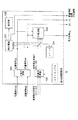
また、この信号処理回路部6における同期回路103の構成については、図16の(A)乃至(C)と同様のものでよい。一方、判定回路107については、図22に示すような構成、あるいは、図23に示すような構成のものとする。
【0313】
即ち、図22に示す構成においては、OPアンプと抵抗値の等しい2つの抵抗とを用い、基準信号(j)を基準とする反転回路107gに、位置信号(b)を入力する。また、1つ目のコンパレータ107hに、位置信号(a)と位置信号(b)とを入力し、2つ目のコンパレータ107iには、位置信号(a)と反転回路107gで作られた位置信号(b)の反転信号とを入力する。そして、これら2つのコンパレータ107h,107iからの出力をAND回路107j、XOR回路107k、NOR回路107lに入力し、これら3つの論理回路107j,107k,107lの出力をラッチ回路107mへ入力する。
【0314】
一方、D−CトリガタイプのLS423などのフリップフロップ107fヘ、データDとして位置信号(c)を、クロックCLKとして位置信号(d)を入力する。そして、フリップフロップ107fの出力Qと原点検出用信号(f)をAND回路107dに入力し、その結果をラッチ回路107mのトリガに入力する。而して、このトリガ信号の立ち上がりでラッチされた3つ信号を、最適同期位置判定結果(判定1〜判定3)とする。
【0315】
また、図23に示す構成においては、OPアンプと抵抗値の等しい2つの抵抗を用い、基準信号(j)を基準とする反転回路107gに、位置信号(b)を入力する。また、1つ目のコンパレータ107hに、位置信号(a)と位置信号(b)とを入力し、2つ目のコンパレータ107iには、位置信号(a)と反転回路107gで作られた位置信号(b)の反転信号とを入力する。
【0316】
そして、これら2つのコンパレータ107h,107iからの出力とそれらの反転信号を4つのAND回路へ入力する。即ち、AND回路107nへはコンパレータ107hの出力とコンパレータ107iの出力とを入力する。AND回路107oへはコンパレータ107hの出力をNOT回路107pで反転した反転信号と、コンパレータ107iの出力とを入力する。AND回路107qへはコンパレータ107hの出力と、コンパレータ107iの出力をNOT回路107rで反転した反転信号とを入力する。そして、AND回路107sへはコンパレータ107hの出力をNOT回路107oで反転した反転信号と、コンパレータ107iの出力をNOT回路107rで反転した反転信号とを入力する。ここで、これらAND回路107n,107o,107q,107sの出力を信号(p),(q),(r),(s)とする。
【0317】
そして、これら信号(p)〜(s)と位置信号(c)及び位置信号(c)の反転信号を8つのAND回路に入力する。即ち、AND回路107tへは信号(p)と位置信号(c)とを入力し、AND回路107uへは信号(q)と位置信号(c)とを入力し、AND回路107vへは信号(r)と位置信号(c)とを入力し、AND回路107wへは信号(s)と位置信号(c)とを入力する。また、AND回路107xへは信号(p)と、位置信号(c)をNOT回路107yで反転した反転信号とを入力し、AND回路107zへは信号(q)と位置信号(c)の反転信号とを入力し、AND回路107Aへは信号(r)と位置信号(c)の反転信号とを入力し、AND回路107Bへは信号(s)と位置信号(c)の反転信号とを入力する。そして、これら8つのAND回路107t〜107x,107z,107A,107Bの出力をラッチ回路107mへ入力する。
【0318】
一方、D−CトリガタイプのLS423などのフリップフロップ107fヘ、データDとして位置信号(c)を、クロックCLKとして位置信号(d)を入力する。そして、フリップフロップ107fの出力Qと原点検出用信号(f)をAND回路107dに入力し、その結果の信号(k)をラッチ回路107mのトリガに入力する。而して、このトリガ信号の立ち上がりでラッチされた8つ信号を、最適同期位置判定結果(判定1〜判定8)とする。
【0319】
また、記憶器109は、SRAMやFLASH ROMなどの不揮発性の記憶媒体を中心に、必要に応じて判定結果の加工や入出力のためのロジックアレイやCPUなどから構成される。この記憶器109では、判定回路107からの判定結果を記憶しておくと共に、外部からの指令に応じて外部へ、記憶している判定結果を出力すると共に、その判定結果をスイッチ104へ送り、最適と判断した同期位置に切り替えるよう構成される。
【0320】
[作用]
本実施の形態における信号処理回路部6によって、図25に示したような光検出器5からの入力を処理する際のタイムチャートは、前述した第1の実施の形態における図2のそれと同様であるので、以下の説明は、図2を参照して行う。
【0321】
即ち、まず、2値化回路101において、変位に伴い周期的に変化するエンコーダのアナログ位置信号(a),(b)を2値化することによって、デジタル位置信号(c),(d)が得られる。
【0322】
また、2値化回路102において、原点検出用信号(e)を所定のスライスレベルで2値化することによって、デジタル原点検出用信号(f)が得られる。
【0323】
そして、原点信号については、次の2つの方法のうちから1つを選択することで得られる。
【0324】
1つ目は、同期回路103の検出回路103kにおいて、デジタル原点検出用信号(f)を位置信号(a),(c)の立ち上がりに同期させてハイレベルとし、位置信号(b),(d)のレベル変化に同期させてローレベルとすることで、原点信号(g)を得るものである。ここで、アナログ信号である位置信号(a),(b)のレベル変化とは、基準信号(j)のレベルの下から上、または、上から下へのレベル変化を指す。
【0325】
2つ目は、同期回路103の検出回路103lにおいて、デジタル原点検出用信号(f)を位置信号(a),(c)の立ち下がりに同期させてハイレベルとし、位置信号(b),(d)のレベル変化に同期させてローレベルとすることで、原点信号(h)を得るものである。
【0326】
これら2つのうちの1つを選択して原点信号(g)または(h)として出力するが、この選択はスイッチ104により行う。
【0327】
ここで、原点信号(g)について、図16の(B)に基づき、より詳細に説明する。
【0328】
まず、方向判別について説明する。フリップフロップ103k1のデータDへは位置信号(d)を、クロックCLKへは位置信号(c)を入力する。この結果、フリップフロップ103k1のQバー出力から出力される信号は、位置信号(c)の立ち上がりの度に位置信号(d)の反転信号として更新される。そのため、位置信号(c)の立ち上がり時に位置信号(d)がローレベルの時のみフリップフロップ103k1のQバー出力がハイレベルとなるため、方向判別が可能となる。
【0329】
そして、AND回路103k2により、このような検出方向判別信号と原点検出信号(f)の論理積を取ることで、検出方向が正しく、原点検出信号(f)が検知状態である場合に限定する。
【0330】
また、更に原点信号を出すための条件を追加する。即ち、本実施の形態では、位置信号(c)の立ち上がりから位置信号(d)の立ち上がりまでを検出する。位置信号(c)の立ち上がりエッジが重要な点であり、検出幅については時間で指定したり、測定対象物の変位量で指定してもよく、幅そのものも任意に指定して構わない。方向が指定された上で、位置信号(c)の立ち上がりから位置信号(d)の立ち上がりまでという場合、位置信号(c)がハイレベルで位置信号(d)がローレベルであることと等価である。従って、この条件を付加する。
【0331】
つまり、以上のことから、原点信号(g)は、位置信号(c)がハイレベルであること、位置信号(d)がローレベルであること、方向判別として位置信号(c)の立ち上がり時に位置信号(d)がローレベルであること、原点検出信号(f)がハイレベル(検知状態)であること、の4つの論理積を取ることで、得られる。
【0332】
なお、位置信号(a),(b)と(c),(d)の組合せは、90°の位相差を持つ。また、アナログ信号である位置信号(a),(b)と原点検出用信号(e)とは、デジタル信号である位置信号(c),(d)と原点検出用信号(f)を作り出すことができるものであれば、それらがどのようなタイプの信号でも構わない。また、図25に示したような光検出器5からの入力がデジタル信号のみで、アナログ信号を含まなくても構わない。また、入力されるアナログの位置信号をデジタル化する際には、さらに、位相分割により分解能を向上させたものとしても構わない。
【0333】
そして、位置検出は、デジタル位置信号(c),(d)を図示しないカウンタに入力することによって行う。この場合、原点信号(g)または(h)が発生したときに、カウンタをリセットすることによって、位置検出の原点出しが可能となる。
【0334】
なお、図4は、図2とは逆方向に変位が生じた際の各信号の変化を示している。この時、アナログ位置信号(a),(b)及びデジタル位置信号(c),(d)の位相の進みは逆転している。
【0335】
このように逆方向に変位が生じるとき、同期回路103は、図16の(A)(及び(C))に示すような構成及びその作用により、原点信号(g)及び(h)を検出状態としない。従って、逆方向の変位では原点検出はなされない。なお、図16の(A)乃至(C)に示す同期回路103を適切に設計することにより、逆方向の変位でのみ原点検出を可能とすることもできる。
【0336】
一方、判定回路107では、原点検出用信号(f)を検知した時点での位置信号(c)の位相が、最も近い立ち上がり(位相0°とする)と立ち下がり(位相180°とする)の内、どちらに近いかを段階的に判定して、位相差の大きい方を安定と見なして出力する。この最適同期位置判定結果は、表示器108へ出力されると共に、記憶器109に記憶される。
【0337】
ここで、図24の(A)及び(B)を参照して、判定のためのエリア分けを説明する。なお、これらの図において、横軸は位置信号(a)のレベルを、また、縦軸は位置信号(b)のレベルを表す。
【0338】
2つの位置信号(a),(b)は90°の位相差と等しい振幅を持つため、ある時点での2つの位置信号により決まる点は、振幅の1/2の半径のリサージュ円周上にある。この点は、時間と伴にリサージュ円周上を右回り、または、左回りに、変位に応じた量だけ動く。図24の(A)及び(B)中の同期位置1は位置信号(a),(c)の立ち上がりであり、同期位置2は位置信号(a),(c)の立ち下がりである。
【0339】
図24の(A)において、第1象限の位置信号(a)の正の側から反時計回りに(1)〜(4)のエリア分けをする。原点検出用信号(f)の立ち上がりにおいて位置信号(a),(b)により決まる点が、これら(1)〜(4)のどのエリアにあるかで、同期位置の判定を行う。
【0340】
即ち、(2)のエリアにある場合、同期位置1に対して位相差が大きいので、同期位置1を判定結果とする。
【0341】
(1)又は(3)のエリアにある場合には、同期位置1,2のどちらに対しても45°以上の余裕があるので、どちらでもよいとの判定結果とする。
【0342】
そして、(4)のエリアにある場合には、同期位置2に対して位相差が大きいので、同期位置2を判定結果とする。
【0343】
このエリア分けについては、図22の構成の判定回路107を使用する場合には、以下の2つの判定により行う。
【0344】
位置信号(a)>位置信号(b) (論理式1)
位置信号(a)>位置信号(b)の反転信号 (論理式2)
これら論理式1と論理式2について、共に真の場合、一方のみ真の場合、共に偽の場合、の3通りについて判定を行う。所定の進行方向であり、原点検出用信号(f)の立ち上がり時に、判定結果をラッチして出力する。
【0345】
また、図24の(B)において、第1象限の位置信号(a)の正の側から反時計回りに(1)〜(8)のエリア分けをする。原点検出用信号(f)の立ち上がりにおいて位置信号(a),(b)により決まる点が、これら(1)〜(8)のどのエリアにあるかで、同期位置の判定を行う。
【0346】
即ち、(2)又は(3)のエリアにある場合、同期位置1に対して位相差が大きいので、同期位置1を判定結果とする。
【0347】
(1)又は(4)のエリアにある場合には、どちらかと言えば同期位置1に対して90°以上の余裕があるので、どちらかと言えば同期位置1との判定結果とする。
【0348】
(5)又は(8)のエリアにある場合には、どちらかと言えば同期位置2に対して90°以上の余裕があるので、どちらかと言えば同期位置2との判定結果とする。
【0349】
そして、(6)又は(7)のエリアにある場合には、同期位置2に対して位相差が大きいので、同期位置2を判定結果とする。
【0350】
上記のように8つのエリアを4つにまとめて判定に用いてもよく、その場合には、図23の各判定結果を上記区分についてAND回路を用いてまとめればよい。
【0351】
エリア分けについては、図22の構成の判定回路107を使用する場合には、以下の3つの判定により行う。
【0352】
位置信号(a)>位置信号(b) (論理式3)
位置信号(a)>位置信号(b)の反転信号 (論理式4)
位置信号(c)のレベル(真偽) (論理式5)
れらの論理式3、論理式4、論理式5について、それぞれの取りうる真偽の組み合わせが8通りある。
【0353】
共に真の場合、一方のみ真の場合、共に偽の場合の判定を行う。所定の進行方向であり、原点検出用信号(f)の立ち上がり時に、判定結果をラッチして出力する。
【0354】
なお、表示器108は、結果が示せるものであれば、どのようなタイプの物でも良いが、例えば、複数のLEDを有しており、立ち上がり及び立ち下がりの内、最適な方に対応したLEDと安定度を示すLEDとを原点検出時に点灯するものや、安定度のみならず位相関係までに対応したLEDを点灯させるものとすることができる。
【0355】
[効果]
原点検出用信号の出力の仕方に応じて位置信号との同期位置を選択することが可能である。従って、信号ノイズやふらつき、更には、光学式のエンコーダでは光源の安定性、発光・受光素子の温度特性とそのばらつき、個々のエンコーダの設計とのずれなどの不安定要素によって生じ得る原点検出位置のずれを少なくする同期位置を選択することが可能である。
【0356】
例えば、上記不安定要素により、図2の原点検出用信号(e)の出力レベルが上がったり、図中左方向にシフトしたり、スライスレベルが若干下がることが考えられる。このとき、原点検出用信号(e)が太線から細線のように変化したとすると、デジタル原点検出用信号(f)は破線のようになる。これにより、原点信号(h)においては破線で示した1周期分ずれた位置が原点信号として検出される。これに対して、原点信号(g)ではこのような変化は起きにくい。従って、原点信号(g)を選択することで、原点検出精度の劣化を抑え、安定した原点検出が可能となる。
【0357】
また、原点信号の位置信号への同期をとるに当たり、複数の同期位置の内、どれが最良かを判断する判定回路107を有しており、実際にエンコーダを装置に取り付けた状態で最良の同期位置を選ぶことができる。本実施の形態においては、位相余裕の大きい方の同期位置を選択することにより、変動などに対する安定性を向上させることが可能となっている。このことにより、位置信号に同期させた原点検出の安定性が増すと共に、エンコーダの取付け時のヘッドとスケールの取付け角度やギャップ等といった相対位置や姿勢のばらつきの影響を事前に考慮する必要が無くなる。即ち、位置信号と原点信号の位相差を厳密に設計や製作において設定して加工する必要がないため、製作コストや組立調整の時間短縮につながると共に、設計や製作上の制約が減ることによって機能上の自由度が上がり得る利点がある。
【0358】
また、本実施の形態においては、立ち上がりと立ち下がりのどちらを選ぶかの判定手段として原点検出用信号の他に2つの位置信号のみを処理する回路を用いており、その時の表示器108も2つのLED程度であり、追加することによる負担も軽い割に位置信号に同期させた原点検出の安定性が容易に実現できる。
【0359】
また、本実施の形態では、信号処理回路部6を除いて原点検出のための補助信号発生用部材などを設けていない。従って、安定した原点検出ができ、且つ、小型で安価なエンコーダを供給することが可能である。
【0360】
更に、一定方向に変位がなされているときのみ原点検出が可能である。これにより、可動部のバックラッシュの影響を受けにくくしたり、原点検出時に2重に原点検出をせずに済ませることにつながるなどの利点が生まれ、高精度で使い勝手のよい原点検出が可能となる。
【0361】
また、本実施の形態では、記憶器109に経時的に逐次保存される判定結果よりシステムとしての挙動が確認できる。例えば、図24の(B)の区分において、ある区分結果から1つ隣の区分結果へ移ることは可動体の構成や検出系の若干の変動により生じる可能性があり、また、許容できるとしても、一定以上変動したり、測定の度に異なる結果が得られる場合には問題があると判断できる。また、原点位置も原点出し後の変動さえなければ良い場合には、例えばシステムの立ち上げ時に原点出しを行い、その際に最適な同期位置を毎回選び直すことも可能となり、経時的な緩やかな変動に対して自己調整が可能となる。
【0362】
以上、実施の形態に基づいて本発明を説明したが、本発明は上述した実施の形態に限定されるものではなく、本発明の要旨の範囲内で種々の変形や応用が可能なことは勿論である。
【0363】
【発明の効果】
従って、以上説明したように、本発明によれば、特に、変位検出に用いられるエンコーダにおいて、AB相に同期した原点検出が安定して行えるエンコーダを提供することができる。
【0364】
また、本発明によれば、判定回路を実装しているため、その判定結果を参照し、それに従ってスイッチを切り替えることができ、特別な治工具無しに、正しい設定の選択が可能となり、その結果として安定した原点検出が可能となる。
【図面の簡単な説明】
【図1】本発明の第1の実施の形態に係るエンコーダにおける信号処理回路部の構成を示すブロック図である。
【図2】図1の信号処理回路によって光検出器からの入力が処理されている様子を示すタイムチャートである。
【図3】(A)及び(B)はそれぞれ本発明の第2の実施の形態に係るエンコーダにおいて、原点信号(g)または(h)を選択するために、図1におけるスイッチ及びこのスイッチにより切り替えられる同期回路の各詳細な構成を示すブロック図である。
【図4】図2と逆方向に変位が生じた際の各信号の変化の様子を示すタイムチャートである。
【図5】本発明の第3の実施の形態に係るエンコーダの信号処理回路部の構成を示すブロック図である。
【図6】第3の実施の形態に係るエンコーダの信号処理回路部において光検出器からの入力が処理されている様子を示すタイムチャートである。
【図7】本発明の第4の実施の形態に係るエンコーダの主要部の構成を示す図である。
【図8】第4の実施の形態によるエンコーダの信号処理回路部の構成を示すブロック図である。
【図9】図8の信号処理回路部によって光検出器からの入力が処理されている様子を示すタイムチャートである。
【図10】本発明の第5の実施の形態に係るエンコーダの主要部の構成を示す図である。
【図11】第5の実施の形態に係るエンコーダの信号処理回路部(原点検出回路部)の構成を示すブロック図である。
【図12】図11の信号処理回路部(原点検出回路部)によって入力が処理されている様子を示すタイムチャートである。
【図13】本発明の第6の実施の形態に係るエンコーダの信号処理回路部によって入力が処理されている様子を示すタイムチャートである。
【図14】本発明の第7の実施の形態に係るエンコーダの信号処理回路部の構成を示すブロック図である。
【図15】(A)は図14中の同期回路の構成例を示す図であり、(B)は図14中の判定回路の構成例を示す図である。
【図16】(A)及び(C)はそれぞれ本発明の第8の実施の形態に係るエンコーダの信号処理回路部における同期回路の構成を示す図であり、(B)は(A)の回路の具体的な構成を示す図である。
【図17】第8の実施の形態に係るエンコーダの信号処理回路部における判定回路の構成を示す図である。
【図18】本発明の第9の実施の形態に係るエンコーダの信号処理回路部の構成を示すブロック図である。
【図19】本発明の第10の実施の形態に係るエンコーダの信号処理回路部の構成を示すブロック図である。
【図20】(A)及び(B)はそれぞれ位置信号(a),(b)と原点検出用信号(f1),(f2),(f3)との関係を説明するため、位置信号(a),(b)の信号レベルの組合せを2次元のグラフに表した図である。
【図21】本発明の第11の実施の形態に係るエンコーダの信号処理回路部の構成を示すブロック図である。
【図22】第11の実施の形態に係るエンコーダの信号処理回路部における判定回路の構成を示す図である。
【図23】第11の実施の形態に係るエンコーダの信号処理回路部における判定回路の別の構成を示す図である。
【図24】(A)及び(B)はそれぞれ最適同期位置判定のためのエリア分けを説明するための図である。
【図25】本発明の第1の実施の形態に係るエンコーダとして適用される光学式のエンコーダの主要部の構成を示す図である。
【図26】特開平8−261795号公報に示されている従来のエンコーダの構成を示す図である。
【符号の説明】
1 発光部
2 光学素子
3 インデックススケール
3a,3b スリット
4,24 スケール
4a,4b スリット
5 光検出器
5a,5b 光検出部
6 信号処理回路部
10 光源部
21 ベース
22 面発光レーザ
22a,22b ビーム出射口
23 フォトIC
23a 受光アレイ部
23b 受光部
23c 信号処理回路
24a 位置検出パターン
24a 原点検出用パターン
101,102 2値化回路
103 同期回路
103a 立ち上がり検出回路
103b ローレベル検出回路
103c,103f,103j,103k2,103k4,103k5,104a,104b,107d,107e,107j,107n,107o,107q,107s〜107x,107z,107A,107B AND回路
103d 立下り検出回路
103e ハイレベル検出回路
103g 立ち上がり検出部
103h 立ち下り検出部
103i 選択スイッチ
103k,103l 検出回路
103k1,107a,107f フリップフロップ
103k3,107p,107r,107y NOT回路
104 スイッチ
105 位相分割回路
106,107m ラッチ回路
107 判定回路
107b 抵抗
107c コンデンサ
107g 反転回路
107h,107i コンパレータ
107k XOR回路
107l NOR回路
108 表示器
109 記憶器[0001]
BACKGROUND OF THE INVENTION
The present invention relates to an encoder, and more particularly, to an encoder used for displacement detection.
[0002]
[Prior art]
As a general example of a conventional encoder, an optical encoder is known.
[0003]
That is, this optical encoder sequentially irradiates a light source unit combining a light emitting unit such as an LED and an optical element for making the beam light from the light emitting unit a parallel light, and the parallel light from the light source unit. An index scale and a scale, a photodetector arranged on the opposite side of the light source unit as viewed from the scale, and a signal processing circuit unit that processes a signal from the photodetector and outputs it as an encoder signal Has been.
[0004]
In such a configuration, the index scale, the scale, and the light detection unit are composed of portions for position detection and origin detection.
[0005]
That is, the index scale and the scale are provided with slit portions for position detection and origin detection, and the light detection portion is also provided with a light detection portion for position detection and origin detection. These combinations enable position detection and origin detection.
[0006]
And in the target object which detects positions, such as a stage and a motor, the combination of the said light source part and a photodetector is attached to either one of a movable part and a fixed part.
[0007]
The scale is attached to either the movable part or the fixed part.
[0008]
Further, general encoder output signals include the following.
[0009]
First, a sine wave signal having a phase difference of 90 ° or an A-phase signal and a B-phase signal that are pulse (rectangular wave) signals that are output in accordance with the displacement of the movable part of the device, etc. This is a Z-phase signal (origin detection signal) output at the time of detection.
[0010]
If the absolute position of the movable part is unknown when the apparatus is turned on or the position information is cleared, accurate position information can be obtained by detecting the origin.
[0011]
Of the encoders, linear encoders that perform linear position detection often place an origin detection pattern near one end of a linear scale.
[0012]
In a rotary encoder that detects rotational motion, an origin detection pattern is usually arranged at one place on a disk-like scale.
[0013]
Then, the movable portion is moved to detect the origin detection pattern of the scale, and the origin signal is output in synchronization with the AB phase signal as necessary.
[0014]
For example, in Japanese Patent Application Laid-Open No. 8-261695, as shown in FIG. 26, a scale / index scale / light receiving unit is provided with a mechanism for generating and detecting a signal having a period longer than that of the position detection signal.
[0015]
That is, in FIG. 26, a collimator lens 32 that converts light from the light source 31 into parallel light and a main scale 33 are provided.
[0016]
The main scale 33 is provided with a
[0017]
In addition, the index scale 36 fixed to a moving body or a fixed body that moves relative to the main scale 33 and arranged to face the main scale 33 is 4 in order to generate displacement signals having phases different by 90 °.
[0018]
Further, on the opposite side to the light source side of the index scale 36, on the opposite side, the
[0019]
Thus, a reference position auxiliary signal is generated in addition to the displacement signal and the reference position signal, and is used as an index for synchronizing the origin signal with the position detection signal.
[0020]
[Problems to be solved by the invention]
In recent years, as the resolution and accuracy of encoders have increased, the demand for the accuracy of the origin signal has increased, and the same resolution, accuracy, and timing as the AB phase signal can be output in synchronization with the AB phase signal. It has been raised as a request. That is, an origin signal having a narrow detection width and good reproducibility is required. Accordingly, encoders are required to suppress deterioration in origin detection accuracy and detection timing shift due to unstable elements as a system.
[0021]
Instability factors include signal noise and fluctuations, and with optical encoders, stability of the light source, temperature characteristics of light emitting / receiving elements and their variations, stage rattle, gap, and mounting angle change over time, There are head and scale arrangements and posture fluctuations when detecting the origin of the stage to be incorporated.
[0022]
In particular, when the origin detection is synchronized with the AB phase while the AB phase signal and the Z phase signal are detected by separate optical systems, the phase of the A phase or B phase signal and the Z phase signal is accurately synchronized, If the phase difference is not provided, there is a possibility that the origin is a position shifted by one cycle of the AB phase signal due to a shift in detection timing.
[0023]
In order to solve these problems, an optical encoder often includes an auxiliary signal generating member for detecting the origin. However, the addition of components, special optical systems, and the addition of scale patterns may require an increase in head size and scale width, which may lead to an increase in cost, which is contrary to the trend toward miniaturization and cost reduction. Prone.
[0024]
The present invention has been made in view of the above circumstances, and in particular, it is an object of the present invention to provide an encoder capable of stably performing origin detection synchronized with the AB phase in an encoder used for displacement detection.
[0025]
[Means for Solving the Problems]
According to the present invention, in order to solve the above problems, (1) position signal generating means for generating a periodic signal in accordance with the displacement of the position or angle of the moving body, and the origin when the moving body is at a predetermined position An origin detection means for generating a signal, a synchronization means for synchronizing the generation position of the origin signal with a position where the periodic signal takes a predetermined phase, and one of a plurality of predetermined phases is selected as the predetermined phase. A switchable selection means; A determination means for detecting an optimum phase among the plurality of phases, Have The selecting means can select the phase taken by the periodic signal at the origin signal generation position based on the determination result from the determining means. Do , An encoder is provided.
[0027]
Further, according to the present invention, in order to solve the above problems, 2 ) It has origin detection signal generation means for generating an origin detection signal when the moving body is in a predetermined range, and the determination means generates the phase and origin signal taken by the periodic signal when the origin detection signal is generated. The optimum phase is detected based on the phase difference from the phase that the periodic signal can take at the position. ,thing An encoder according to (1) is provided.
[0028]
Further, according to the present invention, in order to solve the above problems, 3 ) When the phase difference between the phase that the periodic signal takes when the origin detection signal is generated and the phase that the periodic signal can take at the origin signal generation position is represented by 0 ° to 180 °, It is determined that the phase that can be taken by the periodic signal with the largest value is the optimum ( 2 ) Is provided.
[0029]
Further, according to the present invention, in order to solve the above problems, 4 (1) to (2) having two phase signals of 90 ° phase difference and two of the plurality of phases, and the phase difference between the two phases is 180 °. 3 ) Is provided.
[0030]
Further, according to the present invention, in order to solve the above problems, 5 ) A phase or value at which the periodic signal or the digitized periodic signal crosses the median amplitude from the lower value side to the higher value side with the displacement of the position or angle of the moving body. The phase intersecting from the higher value side to the lower value side is defined as the phase of the periodic signal at the origin detection position ( 4 ) Is provided.
[0031]
Further, according to the present invention, in order to solve the above problems, 6 ) The two periodic signals having a phase difference of 90 ° and N (N is an integer of 3 or more) the plurality of phases, and the phase difference between the N phases is (360 ° / N). (1) to (1) characterized in that 3 ) Is provided.
[0033]
Further, according to the present invention, in order to solve the above problems, 7 ) Position signal generating means for generating two periodic signals with a phase difference of 90 ° in accordance with the position or angular displacement of the moving body, and origin detecting signal for generating an origin detecting signal when the moving body is within a predetermined range Signal generating means, origin detecting means for generating an origin signal when the moving body is at a predetermined position, synchronization means for synchronizing the origin signal generation position with a position where the periodic signal takes a predetermined phase, Selection means capable of selecting and switching one of a plurality of defined phases as the predetermined phase; Judgment means for detecting an optimum phase among the plurality of phases And taking one output of the two periodic signals in the horizontal axis direction of the two-dimensional orthogonal coordinate system and the other output in the vertical axis direction, and each of the two periodic signals on the coordinate system. When the waveform determined by the output of the moving object is a Lissajous waveform of the two periodic signals, the waveform drawn with the displacement of the moving body has two or more divisions that can be obtained by dividing the Lissajous waveform of the two periodic signals. The section including the point determined by the two periodic signals can be determined at least when the origin detection signal is generated, and the determination means includes: Based on the above section on the Lissajous waveform where there is a point determined by the two periodic signals when the origin detection signal is generated, the determination by the determination means is performed. And the selection means can select the phase that the periodic signal takes at the origin signal generation position based on the determination result from the determination means. , Characterized by Encoder Is provided.
[0034]
Further, according to the present invention, in order to solve the above problems, 8 ) When the phase difference between the phase on the Lissajous waveform where the point determined by the two periodic signals is present when the origin detection signal is generated and a plurality of phases of the periodic signal is expressed by 0 ° to 180 °, For the combination with a phase, when the minimum value of the phase difference within the section is the phase difference between the section and the phase, the determination means determines that the phase with the largest phase difference is determined to be optimal. Do ( 7 ) Is provided.
[0035]
Further, according to the present invention, in order to solve the above problems, 9 ) Having origin detection signal generating means for generating a plurality of origin detection signals, each of the plurality of phases corresponding to one of the plurality of origin detection signals, and the period by the selection means The origin detection signal corresponding to the predetermined phase of the signal is simultaneously selected, and the origin signal is generated using the origin detection signal corresponding to the predetermined phase of the selected periodic signal (1) To ( 8 ) Is provided.
[0036]
Further, according to the present invention, in order to solve the above problems, 10 ) Having a plurality of the periodic signals, the plurality of phases corresponding to a predetermined phase determined for each of the periodic signals of the plurality of periodic signals, and selecting one of the predetermined phases of the periodic signal by the selecting means (1) through (1), wherein the origin signal generation position can be synchronized with a predetermined phase of the selected periodic signal. 9 ) Is provided.
[0037]
Further, according to the present invention, in order to solve the above problems, 11 ) An encoder that detects the amount of displacement based on a periodic signal generated according to the displacement of the position or angle of the moving body and generates an origin signal when the moving body is within a predetermined range. There , Irradiates light from the light source to the scale provided on the moving body, and receives the returned light at the light receiving unit to detect the position displacement of the moving body Detection means to Irradiating light from the light source or a light source provided separately to the scale and returning the light A light receiving means for receiving light by a light receiving unit provided separately; Origin detection signal when the moving body is within the specified range The appear Origin detection signal generation means and , All the above light sources and all the light receiving parts But Placed and formed on the same substrate at a predetermined interval by a semiconductor process By doing The phase difference between the phase of the periodic signal when the origin detection signal is generated and the phase of the periodic signal at the origin signal generation position is set to a predetermined value. Synchronizing means for synchronizing the origin signal generation position with a position where the periodic signal takes a predetermined phase; , Have An encoder is provided.
[0042]
Further, according to the present invention, in order to solve the above problems,
(18) The encoder according to any one of (9) to (17), further including storage means for storing the detected optimum synchronization position.
[0043]
In the configuration of the above solution, the configuration of the embodiment described later corresponds as follows.
[0044]
Mobile:
Position signal generating means: a
Origin detecting signal generating means: a
Origin detection circuit: signal processing circuit section (origin detection circuit section) 6
Selection means: switch 104
Determination means:
Storage means:
[0045]
DETAILED DESCRIPTION OF THE INVENTION
Embodiments of the present invention will be described below with reference to the drawings.
[0046]
(First embodiment)
[Constitution]
The configuration of the main part of the encoder according to the first embodiment of the present invention is not particularly limited as long as a position signal (position detection signal) and an origin detection signal can be obtained except for the signal processing circuit unit. .
[0047]
For example, a general configuration such as a configuration using an optical encoder as shown in FIG. 25 can be applied.
[0048]
In the example of FIG. 25, an optical encoder is used, but other types such as a magnetic type may be used.
[0049]
That is, as shown in FIG. 25, this optical encoder includes a
[0050]
In such a configuration, among the
[0051]
Also, a combination of a
[0052]
In an object for position detection such as a stage and a motor, the combination of the
[0053]
The
[0054]
Here, signals (A (+), A (−), B (+), B (−)) whose phases are different from each other by 90 ° corresponding to the movement of the
[0055]
The light receiving element of the
[0056]
FIG. 1 is a block diagram showing a configuration of a signal
[0057]
This signal
[0058]
In FIG. 1, the origin signal (g) or (h) is obtained in synchronization with the digital position signals (c) and (d), but the origin signal is synchronized with the analog position signals (a) and (b). Obtaining (g) or (h) can also be realized by a similar function.
[0059]
[Action]
FIG. 2 is a time chart showing how the input from the
[0060]
First, in the
[0061]
The
[0062]
The origin signal can be obtained by selecting one of the following two methods.
[0063]
First, in the synchronizing
[0064]
Second, in the
[0065]
One of these two is selected and output as the origin signal (g) or (h). This selection is performed by the
[0066]
Here, the combination of the position signals (a), (b) and (c), (d) has a phase difference of 90 °.
[0067]
Further, the position signals (a) and (b) that are analog signals and the origin detection signal (e) produce the position signals (c) and (d) that are digital signals and the origin detection signal (f). They can be any type of signal as long as they can. Further, the input from the
[0068]
Position detection is performed by inputting digital position signals (c) and (d) to a counter (not shown). In this case, when the origin signal (g) or (h) is generated, the origin of position detection can be obtained by resetting the counter.
[0069]
As described above, the origin detection signal (e) is digitized to generate the digital origin detection signal (f), and the digital origin detection signal (f) and the position signals (c) and (d) which are periodic signals are obtained. Are synchronized to generate the origin signal (g) or (h).
[0070]
At this time, the origin signal (g) or (h) is generated only at the earliest condition satisfaction timing even if there are a plurality of times that satisfy one cycle condition in one origin detection. It shall be.
[0071]
The same applies to each embodiment described later.
[0072]
[effect]
The synchronization position with the position signal can be selected according to the way of outputting the origin detection signal.
[0073]
Therefore, the origin detection position that may be caused by unstable factors such as signal noise and fluctuations, and stability of the light source in the optical encoder, temperature characteristics and variations of the light emitting / receiving elements, and deviations from the design of the individual encoder It is possible to select a synchronization position that reduces the deviation.
[0074]
For example, it is conceivable that the output level of the origin detection signal (e) in FIG. 2 increases, shifts to the left in the figure, or the slice level slightly decreases due to the unstable element. At this time, if the origin detection signal (e) changes from a thick line to a thin line, the digital origin detection signal (f) becomes a broken line. Thereby, in the origin signal (h), a position shifted by one cycle indicated by a broken line is detected as the origin signal. On the other hand, such a change hardly occurs in the origin signal (g). Therefore, in this case, by selecting the origin signal (g), it is possible to suppress the degradation of the origin detection accuracy and to perform stable origin detection.
[0075]
In this example, except for the signal
[0076]
(Second Embodiment)
[Constitution]
The configuration of the main part of the second embodiment is particularly limited as long as the position signal and the origin detection signal can be obtained except for the signal
[0077]
Further, the configuration of the signal
[0078]
In FIG. 1, the origin signal (g) or (h) is obtained in synchronization with the digital position signals (c) and (d), but in synchronization with the analog position signals (a) and (b). Obtaining the origin signal (g) or (h) can also be realized with a similar function.
[0079]
3A and 3B respectively show the
[0080]
These circuits can be easily and inexpensively manufactured by a generally available logic IC or the like.
[0081]
That is, in FIG. 3A, the position signal (c) rise
[0082]
In FIG. 3B, the position signal (c) falling
[0083]
[Action]
Also in the second embodiment, the input processing from the
[0084]
FIG. 4 is a time chart showing how each signal changes when displacement occurs in the direction opposite to that in FIG.
[0085]
At this time, the phase advance of the analog position signals (a) and (b) and the digital position signals (c) and (d) is reversed.
[0086]
When the displacement occurs in the reverse direction as described above, the
[0087]
Therefore, the origin detection is not performed for the displacement in the reverse direction.
[0088]
Note that by appropriately designing the
[0089]
[effect]
In the second embodiment, the same effect as that of the first embodiment described above can be obtained.
[0090]
A unique effect of this embodiment is that the origin can be detected only when the displacement is made in a certain direction. As a result, there are advantages such as being less susceptible to the influence of backlash of the movable part, and leading to the need to avoid double origin detection at the time of origin detection, making it possible to perform origin detection with high accuracy and ease of use. .
[0091]
(Third embodiment)
[Constitution]
As in the first and second embodiments, the configuration of the main part of the third embodiment is such that a position signal and an origin detection signal can be obtained except for the signal
[0092]
FIG. 5 is a block diagram showing a configuration of the signal
[0093]
The signal
[0094]
In the signal
[0095]
[Action]
FIG. 6 is a time chart showing how the input from the
[0096]
First, the
[0097]
The
[0098]
In the region where the latch signal (i) is at a high level, the origin signal is obtained by selecting one of the following two methods. In this case, it is more accurate to hold the high level until the origin signal is detected, rather than in the region where the latch signal (i) is high. That is, the
[0099]
The origin signal is obtained by selecting one of the following two methods.
[0100]
The first is to obtain an origin signal by setting the
[0101]
Second, in the
[0102]
One of these two is selected and output as the origin signal (g) or (h). This selection is performed by the
[0103]
Here, the combination of the position signals (a), (b) and (c), (d) has a phase difference of 90 °.
[0104]
Further, the position signals (a) and (b) that are analog signals and the origin detection signal (e) produce the position signals (c) and (d) that are digital signals and the origin detection signal (f). They can be any type of signal as long as they can. Further, the input may be only a digital signal and may not include an analog signal.
[0105]
Position detection is performed by inputting digital position signals (c) and (d) to a counter (not shown). In this case, when the origin signal (g) or (h) is generated, the origin of position detection can be obtained by resetting the counter.
[0106]
[effect]
The synchronization position with the position signal can be selected according to the way of outputting the origin detection signal. Therefore, the origin detection position that may be caused by unstable factors such as signal noise and fluctuations, and stability of the light source in the optical encoder, temperature characteristics and variations of the light emitting / receiving elements, and deviations from the design of the individual encoder It is possible to select a synchronization position that reduces the deviation.
[0107]
Further, as an effect peculiar to the present embodiment, since the origin detection signal (e) is held by the
[0108]
If the rising position of the latch signal (i) can be designed and arranged at a position approximately 180 ° ahead of the phase A synchronization position, a margin of ± 180 ° is generated. That is, there is a positional deviation tolerance of ± 1/2 times the pitch of the position signal. Even when it is difficult to set the phase difference between the rising position of the latch signal (i) and the A-phase synchronization position, a margin of ± 90 ° or more is generated by selecting the synchronization position. Therefore, by selecting the origin signal (g) or (h), it is possible to suppress the degradation of the origin detection accuracy and to perform stable origin detection.
[0109]
In this embodiment, an auxiliary signal generating member for detecting the origin is not provided except for the signal
[0110]
Furthermore, the origin detection can be performed only when the origin is displaced in the constant origin direction by adopting the synchronization method having the limiting function with the position signal in the detection direction described in the second embodiment. As a result, there are advantages such as being less susceptible to the influence of backlash of the movable part, and leading to the need to avoid double origin detection at the time of origin detection, making it possible to perform origin detection with high accuracy and ease of use. .
[0111]
(Fourth embodiment)
[Constitution]
FIG. 7 is a diagram showing a configuration of main parts of an encoder according to the fourth embodiment of the present invention. However, the signal processing circuit unit is not particularly limited as long as the position signal and the origin detection signal can be obtained.
[0112]
As shown in FIG. 7, the optical encoder according to the fourth embodiment combines a
[0113]
In such a configuration, among the
[0114]
Further, the combination of the
[0115]
In an object for position detection such as a stage and a motor, the combination of the
[0116]
The
[0117]
The
[0118]
Phase difference α = [one cycle of position signal] × (i + 1/3) (Expression 1)
However, i is an integer.
[0119]
In this embodiment, an optical encoder is used, but other types such as a magnetic encoder may be used.
[0120]
FIG. 8 is a block diagram showing a configuration of the signal
[0121]
That is, the signal
[0122]
In FIG. 8, the origin signal (g) is obtained in synchronization with the digital position signals (c) and (d), but the origin signal (g) is synchronized with the analog position signals (a) and (b). ) Can be achieved with the same function.
[0123]
As will be described later, in this embodiment, the origin signal (g) is detected in synchronization with the position signal (a), but the position signals (b), (c), (d) Even if they are synchronized, the same function can be realized.
[0124]
[Action]
FIG. 9 is a time chart showing how the input from the
[0125]
First, in the
[0126]
The
[0127]
Then, in the
[0128]
Here, the combination of the position signals (a) and (b) and (c) and (d) has a phase difference of 90 °. The position signals (a) and (b) that are analog signals and the origin detection signals (e1), (e2), and (e3) are the digital position signals (c) and (d) and the origin detection signals. Any type of signal may be used as long as the signals (f1), (f2), and (f3) can be generated. Further, the input from the detection system may be only a digital signal and may not include an analog signal. Further, when the position signal is digitized, the resolution may be further improved by phase division.
[0129]
Position detection is performed by inputting digital position signals (c) and (d) to a counter (not shown). When the origin signal (g) is generated, the origin of position detection can be obtained by resetting the counter.
[0130]
[effect]
By selecting one from a plurality of origin detection signals, it is possible to select a synchronization position with the position signal.
[0131]
Therefore, the origin detection position that can be caused by unstable factors such as signal noise and wobbling, and stability of the light source, temperature characteristics and variations of light emitting / receiving elements, and deviations from the design of individual encoders in optical encoders. It is possible to select a synchronization position that reduces the deviation.
[0132]
For example, the output level of the origin detection signals (e1), (e2), and (e3) shown in FIG. 9 changes, shifts in the horizontal direction in the figure, or the slice level slightly increases or decreases due to the unstable element. It is possible. At this time, the origin signal (g) generated using the origin detection signals (e1) and (e3) is relatively stable. However, when the origin detection signal (e2) is used, it is synchronized with the position signal. Because it is close to the position, it tends to be unstable. In this case, there may be a difference of one cycle or more in the obtained origin position, but if only one is always used, there is no practical problem.
[0133]
As a synchronization method, a method of synchronizing the origin detection signal and the position signal while measuring the displacement near the origin detection position is also employed. In this case, it is desirable to use the origin detection signal (e2) having a small difference between the two, and in this case, it has a tolerance of detection position deviation for a maximum of ± 1 period.
[0134]
Therefore, by selecting the origin signal (g) by the method as described above, deterioration of the origin detection accuracy is suppressed, and stable origin detection is possible.
[0135]
(Fifth embodiment)
[Constitution]
FIG. 10 is a diagram showing a configuration of main parts of an encoder according to the fifth embodiment of the present invention.
[0136]
In FIG. 10, the encoder is roughly divided into four parts: a base 21, a
[0137]
The
[0138]
On the
[0139]
The
[0140]
The wavelength of this light source is about 800 nm to 1000 nm, and the light receiving array portion is a silicon-based semiconductor.
[0141]
In the case where light sources having different wavelengths are used, it is possible to cope with the problem by using a light receiving portion that is desirable for detecting the wavelengths.
[0142]
The
[0143]
Here, one of the sum of the signals of every fourth array element of the light
[0144]
Then, the [A (+)-A (-)] signal is output as an A signal, the [B (+)-B (-)] signal is output as a B signal, and the two A signals and B signal are output as encoder signals. In addition, the
[0145]
The
[0146]
Here, the pitch Pp between the elements of the light receiving
[0147]
Pp = 2Ps
The laser beam emitted from the
[0148]
When the laser light is parallel light, the light source, scale, and light receiving unit may be arranged so as to satisfy the imaging condition of the diffraction image.
[0149]
The
[0150]
The gap d is determined so that an image twice as large as the
[0151]
In this embodiment, a diffraction image by reflection on the scale surface is used. However, it is also possible to arrange the light receiving unit above the scale in FIG. 10 using transmitted light. In this case, the gap between the light source and the scale and the gap between the scale and the light receiving unit are selected so that the resolution is high depending on the wavelength and the emission angle, and the distance between the two gaps does not necessarily have to be equal.
[0152]
However, when the two gap amounts are different, the following relationship holds between the scale pitch and the pitch of the light receiving array section.
[0153]
Ps: Pp = (gap amount between light source and scale): (gap amount between light source and scale + gap amount between scale and light receiving unit)
When the
[0154]
Here, the
[0155]
The beam emission interval of the
[0156]
The
[0157]
FIG. 11 is a block diagram showing the configuration of the signal processing circuit unit (origin detection circuit unit) 6 of the encoder according to the fifth embodiment of the present invention.
[0158]
The signal processing circuit unit (origin detection circuit unit) 6 phase-divides the analog position signals A and B and converts them into digital signals (c) and (d), and an origin detection signal (e ) Is binarized at a predetermined slice level and converted to a digital origin detection signal (f), and the origin signal (g) is synchronized with the rising edge of the position signal A. ) To generate a
[0159]
In FIG. 11, the rising edge of the signal A is detected at a point crossing the center of the amplitude, as will be described later.
[0160]
Although the origin signal (g) is obtained in synchronization with the rise of the signal A, an appropriate signal may be selected from the position signals A, B, (c), and (d) and synchronized.
[0161]
[Action]
First, the position detection function as an encoder will be described.
[0162]
Laser light emitted from the
[0163]
When the
[0164]
Since the two electrical signals A and B detected by the light receiving
[0165]
The position detection is performed by inputting digital position signals (c) and (d) to a counter (not shown).
[0166]
Next, the origin detection procedure will be described.
[0167]
FIG. 12 is a time chart showing a state in which an input from the
[0168]
First, in the
[0169]
The
[0170]
Then, in the synchronizing
[0171]
Here, the combination of the position signals (c) and (d) has a phase difference of 90 °.
[0172]
When the origin signal (g) is generated, the origin of position detection can be obtained by resetting a counter (not shown) that counts the origin signal (g).
[0173]
[effect]
The phase difference between the origin detection signal and the position signal can be set to an optimum value in advance by design. Also, the error is several μm or less in terms of accuracy by the semiconductor process. Therefore, the origin detection position that can be caused by unstable factors such as signal noise and wobbling, and the stability of the light source, temperature characteristics of light emitting and receiving elements and their variations, and deviations from the design of individual encoders in optical encoders It is possible to reduce the deviation.
[0174]
Furthermore, when synchronizing the origin signal, the tolerance during assembly and installation can be increased. For example, due to the unstable element, the tolerance for increasing the output level of the origin detection signal (e) shown in FIG. 12, shifting to the left in FIG. 12, or lowering the slice level slightly increases. Degradation of detection accuracy is suppressed and stable origin detection is possible.
[0175]
In this embodiment, no auxiliary signal generating member for detecting the origin is provided except for the signal processing circuit section (origin detection circuit section) 6. Further, even when compared with other embodiments, the synchronization timing changeover switch and the like can be omitted. Therefore, a stable origin can be detected, and a small and inexpensive encoder can be supplied.
[0176]
(Sixth embodiment)
In the sixth embodiment, the encoder detects the displacement of the moving body, generates a plurality of periodic signals according to the movement of the moving body, and when the moving body is at a predetermined position, An origin detection signal is generated, and one periodic signal can be selected from the plurality of periodic signals. Based on the origin detection signal, the moving body is synchronized with the selected periodic signal. It is characterized by detecting that it is at the origin position.
[0177]
[Constitution]
The configuration of the signal processing circuit unit in the encoder according to the sixth embodiment is the same as that of the signal processing circuit unit in the first embodiment described above, but the function of the
[0178]
[Action]
FIG. 13 is a time chart showing how the input from the
[0179]
The origin signal (g) or (h) is obtained by selecting one of the following two methods.
[0180]
The first is to set the high level in synchronization with the fall of the position signal (c) of the digital origin detection signal (f), and to the low level in synchronization with the level change of the position signal (d). A signal (g) is obtained.
[0181]
Second, the digital origin detection signal (f) is set to the high level in synchronization with the falling edge of the position signal (d), and is set to the low level in synchronization with the level change of the position signal (c). The signal (h) is obtained.
[0182]
Such selection of the origin signal (g) or (h) is performed by the
[0183]
The position and the width of the digital origin detection signal (f) obtained by binarizing the origin detection signal (e) with a predetermined slice level change according to the level change of the origin detection signal (e). The position of the origin signal (g) is changed by the change of the digital origin detection signal (f), but the origin signal (h) is not changed.
[0184]
[effect]
Also in the sixth embodiment, the same effects as those in the above-described embodiments can be obtained.
[0185]
(Seventh embodiment)
[Constitution]
The configuration of the main part of the seventh embodiment is not particularly limited as long as the position signal and the origin detection signal can be obtained except for the signal
[0186]
FIG. 14 is a block diagram showing a configuration of the signal
[0187]
The signal
[0188]
15A shows a configuration example of the
[0189]
That is, the
[0190]
In the
[Expression 1]
![]()
[0191]
In FIG. 14, the origin signal (g) or (h) is obtained in synchronization with the position signals (c) and (d). Can be realized.
[0192]
[Action]
The time chart when the input from the
[0193]
That is, first, in the
[0194]
The
[0195]
The origin signal can be obtained by selecting one of the following two methods.
[0196]
First, in the synchronizing
[0197]
Second, in the
[0198]
One of these two is selected and output as the origin signal (g) or (h). This selection is performed by the
[0199]
Here, the combination of the position signals (a), (b) and (c), (d) has a phase difference of 90 °.
[0200]
Further, the position signals (a) and (b) that are analog signals and the origin detection signal (e) produce the position signals (c) and (d) that are digital signals and the origin detection signal (f). They can be any type of signal as long as they can. Further, the input from the
[0201]
Position detection is performed by inputting digital position signals (c) and (d) to a counter (not shown). In this case, when the origin signal (g) or (h) is generated, the origin of position detection can be obtained by resetting the counter.
[0202]
On the other hand, in the
[0203]
The
[0204]
Here, a specific determination method will be described.
[0205]
First, the level of the position signals (c) and (d) is confirmed. In the position signals (c) and (d) in FIG. 2, the phase of the position signal (c) is advanced by 90 °. In this state, the level of the position signal (d) at the rise of the position signal (c) is a low level. Therefore, when the level of the position signal (d) is low, the phase difference until the rising of the position signal (c) is within ± 90 °, and when the level of the position signal (d) is high, the position is The phase difference until the rising edge of the signal (c) is ± 90 ° or more.
[0206]
Therefore, if the level of the position signal (d) at the time of detecting the rising edge of the origin detection signal (f) is high, the rising position of the origin detection signal (f) is synchronized with the rising edge of the position signal (c). It is more stable than the low level for some fluctuations. Based on the same discussion, if the level of the position signal (d) at the time of detecting the rising edge of the origin detection signal (f) is low, the origin detection signal (f) is synchronized with the falling edge of the position signal (c). ) Is more stable than a high level with respect to slight fluctuations in the rising position. Therefore, a more stable synchronization position may be output as a determination result.
[0207]
For example, in FIG. 2, the level of the position signal (d) at the moment (rising edge) when the origin detection signal (f) is detected is shown by a thick line (origin detection signal) of the origin detection signal (e). In the example of (f) solid line), the level is high. Therefore, regarding the nearest rising and falling of the position signal (c), it can be seen that the rising has a larger phase difference and is more stable, and the rising is output as the determination result.
[0208]
[effect]
The synchronization position with the position signal can be selected according to the way of outputting the origin detection signal. Therefore, the origin detection position that can be caused by unstable factors such as signal noise and wobbling, and stability of the light source in the optical encoder, temperature characteristics and variations of the light emitting / receiving elements, and deviation from the design of the individual encoder It is possible to select a synchronization position that reduces the deviation.
[0209]
For example, it is conceivable that the output level of the origin detection signal (e) in FIG. 2 increases, shifts to the left in the figure, or the slice level slightly decreases due to the unstable element. At this time, if the origin detection signal (e) changes from a thick line to a thin line, the digital origin detection signal (f) becomes a broken line. Thereby, in the origin signal (h), a position shifted by one cycle indicated by a broken line is detected as the origin signal. On the other hand, such a change hardly occurs in the origin signal (g). Therefore, by selecting the origin signal (g), it is possible to suppress the degradation of the origin detection accuracy and perform stable origin detection.
[0210]
In the present embodiment, in order to synchronize the origin signal with the position signal, the
[0211]
In this case, in the present embodiment, it is possible to improve the stability against fluctuation and the like by selecting the synchronization position having the larger phase margin. This increases the stability of origin detection synchronized with the position signal, and eliminates the need to consider in advance the effects of variations in relative position and orientation, such as the mounting angle and gap between the head and scale when the encoder is mounted. . In other words, it is not necessary to set and process the phase difference between the position signal and the origin signal strictly in design and production, leading to reduction in production cost and assembly adjustment time, and function by reducing design and production restrictions. There is an advantage that the degree of freedom can be increased.
[0212]
In the present embodiment, a circuit for processing only two position signals in addition to the origin detection signal is used as means for determining whether to select rising or falling, and the
[0213]
Further, in the present embodiment, an auxiliary signal generating member for detecting the origin is not provided except for the signal
[0214]
(Eighth embodiment)
[Constitution]
As in the seventh embodiment, the configuration of the main part of the eighth embodiment is not particularly limited as long as the position signal and the origin detection signal can be obtained except for the signal
[0215]
Further, the configuration of the signal
[0216]
16A to 16C are diagrams illustrating the configuration of the
[0217]
The position signal having a 90 ° phase difference reverses the phase advancement when the detection direction changes. Using this fact, the direction can be determined. That is, when the position signal (c) rises, the position signal (d) becomes low or high depending on the detection direction (stage moving direction). Therefore, the direction can be determined by defining the level of the position signal (d). Therefore, in the
[0218]
FIG. 16C shows the configuration of the synchronizing
[0219]
FIG. 17 is a diagram illustrating a configuration example of the
[0220]
That is, the position signal (c) is input as the data D and the position signal (d) is input as the clock CLK to the flip-
[0221]
[Action]
The time chart when the input from the
[0222]
That is, first, the
[0223]
The
[0224]
The origin signal can be obtained by selecting one of the following two methods.
[0225]
First, in the
[0226]
Second, in the detection circuit 103l of the
[0227]
One of these two is selected and output as the origin signal (g) or (h). This selection is performed by the
[0228]
Here, the origin signal (g) will be described in more detail based on FIG.
[0229]
First, direction determination will be described. The position signal (d) is input to the data D of the flip-flop 103k1, and the position signal (c) is input to the clock CLK. As a result, the signal output from the Q-bar output of the flip-flop 103k1 is updated as an inverted signal of the position signal (d) every time the position signal (c) rises. Therefore, only when the position signal (d) is at the low level when the position signal (c) rises, the Q bar output of the flip-flop 103k1 is at the high level, so that the direction can be determined.
[0230]
Then, the AND circuit 103k2 calculates the logical product of such a detection direction determination signal and the origin detection signal (f), so that the detection direction is correct and the origin detection signal (f) is in the detection state.
[0231]
Further, a condition for outputting the origin signal is added. That is, in the present embodiment, the period from the rising edge of the position signal (c) to the rising edge of the position signal (d) is detected. The rising edge of the position signal (c) is an important point, and the detection width may be specified by time, may be specified by the amount of displacement of the measurement object, or the width itself may be arbitrarily specified. When the direction is designated and the rising edge of the position signal (c) is followed by the rising edge of the position signal (d), it is equivalent to the position signal (c) being high level and the position signal (d) being low level. is there. Therefore, this condition is added.
[0232]
That is, from the above, the origin signal (g) is detected when the position signal (c) is at a high level, the position signal (d) is at a low level, and when the position signal (c) rises as a direction determination. It is obtained by taking the four logical products of the signal (d) being at a low level and the origin detection signal (f) being at a high level (detection state). That is, the AND circuit 103k4 takes the logical product of the position signal (c) and the position signal (d) inverted by the NOT circuit 103k3, and the logical product of the output of the AND circuit 103k4 and the output of the AND circuit 103k2 is the AND circuit. The origin signal (g) is obtained by taking at 103k5.
[0233]
The combination of the position signals (a), (b) and (c), (d) has a phase difference of 90 °. Further, the position signals (a) and (b) that are analog signals and the origin detection signal (e) produce the position signals (c) and (d) that are digital signals and the origin detection signal (f). They can be any type of signal as long as they can. Further, the input from the
[0234]
Position detection is performed by inputting digital position signals (c) and (d) to a counter (not shown). In this case, when the origin signal (g) or (h) is generated, the origin of position detection can be obtained by resetting the counter.
[0235]
FIG. 4 shows changes in signals when displacement occurs in the direction opposite to that in FIG. At this time, the phase advance of the analog position signals (a) and (b) and the digital position signals (c) and (d) is reversed.
[0236]
When the displacement occurs in the reverse direction as described above, the
[0237]
On the other hand, in the
[0238]
The
[0239]
Here, a specific determination method will be described.
[0240]
First, the level of the position signals (c) and (d) is confirmed. In the position signals (c) and (d) in FIG. 2, the phase of the position signal (c) is advanced by 90 °. In this state, the level of the position signal (d) at the rise of the position signal (c) is a low level. Therefore, when the level of the position signal (d) is low, the phase difference until the rising of the position signal (c) is within ± 90 °, and when the level of the position signal (d) is high, the position is The phase difference until the rising edge of the signal (c) is ± 90 ° or more.
[0241]
Therefore, if the level of the position signal (d) at the time of detecting the rising edge of the origin detection signal (f) is low, the rising position of the origin detection signal (f) is synchronized with the rising edge of the position signal (c). It is more stable than the high level against some fluctuations. Based on the same discussion, if the level of the position signal (d) at the time of detecting the rising edge of the origin detection signal (f) is high, the origin detection signal (f) is synchronized with the falling edge of the position signal (c). ) Is more stable than the low level with respect to slight fluctuations in the rising position. Therefore, a more stable synchronization position may be output as a determination result.
[0242]
For example, in FIG. 2, the level of the position signal (d) at the moment when the origin detection signal (f) is detected (at the time of rising) is the same as that of the origin detection signals (e) and (f) in FIG. High level. Therefore, regarding the closest rising and falling of the position signal (c), it is found that the falling has a larger phase difference and is stable, and the falling is output as the determination result.
[0243]
FIG. 17 shows such a determination method as a specific circuit.
[0244]
That is, the direction determination is performed using the position signal (c) and the position signal (d) by the flip-
[0245]
When the detection direction is the designated direction,
[0246]
[effect]
The synchronization position with the position signal can be selected according to the way of outputting the origin detection signal. Therefore, the origin detection position that can be caused by unstable factors such as signal noise and wobbling, and stability of the light source in the optical encoder, temperature characteristics and variations of the light emitting / receiving elements, and deviation from the design of the individual encoder It is possible to select a synchronization position that reduces the deviation.
[0247]
For example, it is conceivable that the output level of the origin detection signal (e) in FIG. 2 increases, shifts to the left in the figure, or the slice level slightly decreases due to the unstable element. At this time, if the origin detection signal (e) changes from a thick line to a thin line, the digital origin detection signal (f) becomes a broken line. Thereby, in the origin signal (h), a position shifted by one cycle indicated by a broken line is detected as the origin signal. On the other hand, such a change hardly occurs in the origin signal (g). Therefore, by selecting the origin signal (g), it is possible to suppress the degradation of the origin detection accuracy and perform stable origin detection.
[0248]
In order to synchronize the origin signal with the position signal, a
[0249]
In the present embodiment, a circuit for processing only two position signals in addition to the origin detection signal is used as means for determining whether to select rising or falling, and the
[0250]
Further, in the present embodiment, an auxiliary signal generating member for detecting the origin is not provided except for the signal
[0251]
Furthermore, as an effect peculiar to the eighth embodiment, it is possible to detect the origin only when the displacement is made in a certain direction. As a result, there are advantages such as being less susceptible to the influence of backlash of the movable part, and leading to the need to avoid double origin detection at the time of origin detection, making it possible to perform origin detection with high accuracy and ease of use. .
[0252]
(Ninth embodiment)
[Constitution]
In the ninth embodiment of the present invention, the optimum synchronization position determining means as in the seventh embodiment is added to the above-described third embodiment.
[0253]
As in the seventh embodiment, the configuration of the main part of the ninth embodiment is not particularly limited as long as the position signal and the origin detection signal can be obtained except for the signal
[0254]
FIG. 18 is a block diagram showing the configuration of the signal
[0255]
The signal
[0256]
In the signal
[0257]
[Action]
The time chart when the input from the
[0258]
That is, first, in the
[0259]
The
[0260]
The origin signal is obtained by selecting one of the following two methods.
[0261]
The first is to obtain an origin signal by setting the
[0262]
Second, in the
[0263]
One of these two is selected and output as the origin signal (g) or (h). This selection is performed by the
[0264]
The combination of the position signals (a), (b) and (c), (d) has a phase difference of 90 °. Further, the position signals (a) and (b) that are analog signals and the origin detection signal (e) produce the position signals (c) and (d) that are digital signals and the origin detection signal (f). They can be any type of signal as long as they can. Further, the input may be only a digital signal and may not include an analog signal.
[0265]
Position detection is performed by inputting digital position signals (c) and (d) to a counter (not shown). In this case, when the origin signal (g) or (h) is generated, the origin of position detection can be obtained by resetting the counter.
[0266]
On the other hand, in the
[0267]
The
[0268]
Here, a specific determination method will be described.
[0269]
First, the level of the position signals (c) and (d) is confirmed. In the position signals (c) and (d) in FIG. 6, the phase of the position signal (c) is advanced by 90 °. In this state, the level of the position signal (d) at the rise of the position signal (c) is a low level. Therefore, when the position detection signal (d) is at a low level when the origin detection (f) signal is detected, the phase difference until the rising edge of the position signal (c) is within ± 90 °. When the level of (d) is high, the phase difference until the rise of the position signal (c) is ± 90 ° or more.
[0270]
Therefore, if the level of the position signal (d) at the time of detecting the rising edge of the origin detection signal (f) is high, the rising position of the origin detection signal (f) is synchronized with the rising edge of the position signal (c). It is more stable than the case of synchronizing with the falling with respect to slight fluctuations. Based on the same discussion, if the level of the position signal (d) at the time of detecting the rising edge of the origin detection signal (f) is low, the origin detection signal (f) is synchronized with the falling edge of the position signal (c). ) Is more stable than a case where the rise position is synchronized with the rise. Therefore, a more stable synchronization position may be output as a determination result.
[0271]
For example, in FIG. 6, the level of the position signal (d) at the moment (at the time of rising) when the origin detection signal (f) is detected is the level of the origin detection signals (e) and (f) as shown in FIG. In the example, it is high level. Therefore, regarding the nearest rising and falling of the position signal (c), it can be seen that the rising has a larger phase difference and is more stable, and the rising is output as the determination result.
[0272]
[effect]
The synchronization position with the position signal can be selected according to the way of outputting the origin detection signal. Therefore, the origin detection position that can be caused by unstable factors such as signal noise and wobbling, and stability of the light source in the optical encoder, temperature characteristics and variations of the light emitting / receiving elements, and deviation from the design of the individual encoder It is possible to select a synchronization position that reduces the deviation.
[0273]
Further, as an effect peculiar to the ninth embodiment, since the origin detection signal (e) is held by the
[0274]
If the rising position of the latch signal (i) can be designed and arranged at a position approximately 180 ° ahead of the synchronization position of the position signal (c), a margin of ± 180 ° is generated. That is, there is a positional deviation tolerance of ± 1/2 times the pitch of the position signal. Even when it is difficult to set the phase difference between the rising position of the latch signal (i) and the A-phase synchronization position, a margin of ± 90 ° or more is generated by selecting the synchronization position. Therefore, by selecting the origin signal (g) or (h), it is possible to suppress the degradation of the origin detection accuracy and to perform stable origin detection.
[0275]
Furthermore, in this embodiment, when synchronizing the origin signal with the position signal, the
[0276]
In this case, in the present embodiment, it is possible to improve the stability against fluctuation and the like by selecting the synchronization position having the larger phase margin. This increases the stability of origin detection synchronized with the position signal, and eliminates the need to consider in advance the effects of variations in relative position and orientation, such as the mounting angle and gap between the head and scale when the encoder is mounted. . In other words, it is not necessary to set and process the phase difference between the position signal and the origin signal strictly in design and production, leading to reduction in production cost and assembly adjustment time, and function by reducing design and production restrictions. There is an advantage that the degree of freedom can be increased.
[0277]
In the present embodiment, a circuit for processing only two position signals in addition to the origin detection signal is used as means for determining whether to select rising or falling, and the
[0278]
Further, in the present embodiment, an auxiliary signal generating member for detecting the origin is not provided except for the signal
[0279]
Furthermore, if a synchronization method having a limiting function with the position signal in the detection direction as described in the eighth embodiment is adopted, the origin can be detected only when the displacement is made in a certain direction. be able to. As a result, there are advantages such as being less susceptible to the influence of backlash of the movable part, and leading to the need to avoid double origin detection at the time of origin detection, making it possible to perform origin detection with high accuracy and ease of use. .
[0280]
(Tenth embodiment)
[Constitution]
In the tenth embodiment of the present invention, the optimum synchronization position determination means as in the seventh embodiment is added to the above-described fourth embodiment.
[0281]
The main configuration of the encoder according to the present embodiment is the same as that in the above-described fourth embodiment as shown in FIG.
[0282]
FIG. 19 is a block diagram showing a configuration of the signal
[0283]
That is, the signal
[0284]
In FIG. 19, the origin signal (g) is detected in synchronization with the position signal (a), but the same function can be obtained by synchronizing with the position signals (b), (c), and (d). Can be realized.
[0285]
[Action]
The time chart when the input from the
[0286]
First, in the
[0287]
The
[0288]
Then, in the
[0289]
Here, the combination of the position signals (a) and (b) and (c) and (d) has a phase difference of 90 °. The position signals (a) and (b) that are analog signals and the origin detection signals (e1), (e2), and (e3) are the digital position signals (c) and (d) and the origin detection signals. Any type of signal may be used as long as the signals (f1), (f2), and (f3) can be generated. Further, the input from the detection system may be only a digital signal and may not include an analog signal. Further, when the position signal is digitized, the resolution may be further improved by phase division.
[0290]
Position detection is performed by inputting digital position signals (c) and (d) to a counter (not shown). When the origin signal (g) is generated, the origin of position detection can be obtained by resetting the counter.
[0291]
On the other hand, the
[0292]
The
[0293]
Here, a specific determination method will be described.
[0294]
In the position signals (a), (b), (c), and (d) of FIG. 9, the position signals (b) and (d) have a phase of 90 relative to the position signals (a) and (c). ° Advanced. These will be described with reference to FIGS. 20A and 20B. When the combination of the signal levels of the position signals (a) and (b) in FIG. 9 is represented in a two-dimensional graph, the signal moves in the clockwise direction on the circumferences of FIGS. 20 (A) and 20 (B). Here, the level of the position signal (a) changes from minus to plus, that is, the rise of the position signal (c) occurs at the intersection of the vertical axis and the circle indicated by the arrows in FIGS. 20 (A) and 20 (B). Among them, the position signal (b) is an upper point on the plus side. It can be said that the position at the time of detecting the origin detection signal farthest from this point is the most stable against the fluctuation of the system. The three points (f1), (f2), and (f3) in (A) and (B) of FIG. 20 are the positions at the moment when the origin detection signals (f1), (f2), and (f3) are detected. The positions of signals (a) and (b) are shown.
[0295]
If the level of the position signal (d) when the origin detection signal is detected is low, that is, if the position at the time of origin detection signal detection exists in the lower half of the circumference, at least the phase margin is 90 ° or more. Yes, stable. The phase difference of each origin detection signal is known and is approximately 120 °. Therefore, there are one or two origin detection signals at which the level of the position signal (d) when the origin detection signal is detected becomes low.
[0296]
As in the example of FIG. 20A, if there is one origin detection signal that satisfies the condition, it may be determined as the optimum detection signal.
[0297]
On the other hand, if there are two origin detection signals that satisfy the condition as in the example of FIG. 20B, both may be considered stable.
[0298]
Here, if one of the two is narrowed down, the following is performed. That is, in the example of FIG. 20B, there is only one origin detection signal (f2) at which the level of the position signal (d) becomes high. Since the phase difference of each origin detection signal is known and is almost 120 °, the level (low level) opposite to the level (low level) of the position signal (a) (that is, the position signal (c)) at the corresponding point (f2) ( The origin detection signal (f1) corresponding to the point (f1) having the high level) can be determined as the most stable origin detection signal.
[0299]
[effect]
According to the present embodiment, it is possible to select a synchronization position with a position signal by selecting one from a plurality of origin detection signals. Therefore, the origin detection position that can be caused by unstable factors such as signal noise and wobbling, and stability of the light source in the optical encoder, temperature characteristics and variations of the light emitting / receiving elements, and deviation from the design of the individual encoder It is possible to select a synchronization position that reduces the deviation.
[0300]
For example, the output level of the origin detection signals (e1), (e2), and (e3) in FIG. 9 changes due to the unstable element, shifts in the horizontal direction in the figure, and the slice level slightly increases or decreases. Can be considered. At this time, the origin signal (g) generated using the origin detection signals (e1) and (e3) is relatively stable. However, when the origin detection signal (e2) is used, it is synchronized with the position signal. Because it is close to the position, it tends to be unstable. In this case, there may be a difference of one cycle in the obtained origin position, but if only one of them is always used, there is no practical problem.
[0301]
As a synchronization method, a method of synchronizing the origin detection signal and the position signal while measuring the displacement near the origin detection position is also employed. In this case, it is desirable to use the origin detection signal (e2) having a small difference between the two, and in this case, it has a tolerance of detection position deviation for a maximum of ± 1 period.
[0302]
Therefore, by selecting the origin signal (g) by the method as described above, it is possible to suppress the deterioration of the origin detection accuracy and to perform stable origin detection.
[0303]
Furthermore, the present embodiment has a
[0304]
In this case, in the present embodiment, it is possible to improve the stability against fluctuation and the like by selecting the synchronization position having the larger phase margin. This increases the stability of origin detection synchronized with the position signal, and eliminates the need to consider in advance the effects of variations in relative position and orientation, such as the mounting angle and gap between the head and scale when the encoder is mounted. . In other words, it is not necessary to set and process the phase difference between the position signal and the origin signal strictly in design and production, leading to reduction in production cost and assembly adjustment time, and function by reducing design and production restrictions. There is an advantage that the degree of freedom can be increased.
[0305]
In the present embodiment, a circuit for processing only two position signals in addition to the origin detection signal is used as means for determining which of the three origin output signals is selected, and the
[0306]
(Eleventh embodiment)
[Constitution]
Next, an eleventh embodiment of the present invention will be described.
[0307]
The main configuration of the encoder according to the present embodiment is not particularly limited as long as the position signal and the origin detection signal can be obtained, except for the signal
[0308]
The configuration of the
[0309]
That is, the signal
[0310]
In the present embodiment, a reference signal (j) is further given. The reference signal (j) is a signal that is the amplitude center level of the position signal (a) and the position signal (b), and is used in the
[0311]
The
[0312]
Further, the configuration of the
[0313]
That is, in the configuration shown in FIG. 22, the position signal (b) is input to the
[0314]
On the other hand, the position signal (c) is input as the data D and the position signal (d) is input as the clock CLK to the flip-
[0315]
In the configuration shown in FIG. 23, the position signal (b) is input to the
[0316]
Then, the outputs from these two
[0317]
Then, these signals (p) to (s), the position signal (c), and the inverted signal of the position signal (c) are input to eight AND circuits. That is, the signal (p) and the position signal (c) are input to the AND circuit 107t, the signal (q) and the position signal (c) are input to the AND
[0318]
On the other hand, the position signal (c) is input as the data D and the position signal (d) is input as the clock CLK to the flip-
[0319]
The
[0320]
[Action]
The time chart when the input from the
[0321]
That is, first, the
[0322]
The
[0323]
The origin signal can be obtained by selecting one of the following two methods.
[0324]
First, in the
[0325]
Second, in the detection circuit 103l of the
[0326]
One of these two is selected and output as the origin signal (g) or (h). This selection is performed by the
[0327]
Here, the origin signal (g) will be described in more detail based on FIG.
[0328]
First, direction determination will be described. The position signal (d) is input to the data D of the flip-flop 103k1, and the position signal (c) is input to the clock CLK. As a result, the signal output from the Q-bar output of the flip-flop 103k1 is updated as an inverted signal of the position signal (d) every time the position signal (c) rises. Therefore, only when the position signal (d) is at the low level when the position signal (c) rises, the Q bar output of the flip-flop 103k1 is at the high level, so that the direction can be determined.
[0329]
Then, the AND circuit 103k2 calculates the logical product of such a detection direction determination signal and the origin detection signal (f), so that the detection direction is correct and the origin detection signal (f) is in the detection state.
[0330]
Further, a condition for outputting the origin signal is added. That is, in the present embodiment, the period from the rising edge of the position signal (c) to the rising edge of the position signal (d) is detected. The rising edge of the position signal (c) is an important point, and the detection width may be specified by time, may be specified by the amount of displacement of the measurement object, or the width itself may be arbitrarily specified. When the direction is designated and the rising edge of the position signal (c) is followed by the rising edge of the position signal (d), it is equivalent to the position signal (c) being high level and the position signal (d) being low level. is there. Therefore, this condition is added.
[0331]
That is, from the above, the origin signal (g) is detected when the position signal (c) is at a high level, the position signal (d) is at a low level, and when the position signal (c) rises as a direction determination. It is obtained by taking the four logical products of the signal (d) being at a low level and the origin detection signal (f) being at a high level (detection state).
[0332]
The combination of the position signals (a), (b) and (c), (d) has a phase difference of 90 °. Further, the position signals (a) and (b) that are analog signals and the origin detection signal (e) produce the position signals (c) and (d) that are digital signals and the origin detection signal (f). They can be any type of signal as long as they can. Further, the input from the
[0333]
Position detection is performed by inputting digital position signals (c) and (d) to a counter (not shown). In this case, when the origin signal (g) or (h) is generated, the origin of position detection can be obtained by resetting the counter.
[0334]
FIG. 4 shows changes in signals when displacement occurs in the direction opposite to that in FIG. At this time, the phase advance of the analog position signals (a) and (b) and the digital position signals (c) and (d) is reversed.
[0335]
When the displacement occurs in the reverse direction as described above, the
[0336]
On the other hand, in the
[0337]
Here, with reference to FIGS. 24A and 24B, area division for determination will be described. In these drawings, the horizontal axis represents the level of the position signal (a), and the vertical axis represents the level of the position signal (b).
[0338]
Since the two position signals (a) and (b) have an amplitude equal to the phase difference of 90 °, the point determined by the two position signals at a certain time point is on the Lissajous circumference having a radius of ½ of the amplitude. is there. This point moves clockwise or counterclockwise on the Lissajous circle with time by an amount corresponding to the displacement. In FIGS. 24A and 24B, the
[0339]
In FIG. 24A, the areas (1) to (4) are divided counterclockwise from the positive side of the position signal (a) in the first quadrant. The synchronization position is determined according to which area (1) to (4) the point determined by the position signals (a) and (b) at the rising edge of the origin detection signal (f) is.
[0340]
That is, in the area (2), since the phase difference is large with respect to the
[0341]
If it is in the area of (1) or (3), there is a margin of 45 ° or more with respect to either of the
[0342]
And when it exists in the area of (4), since a phase difference is large with respect to the
[0343]
This area division is performed by the following two determinations when the
[0344]
Position signal (a)> Position signal (b) (Logical expression 1)
Position signal (a)> Inverted signal of position signal (b) (Logical expression 2)
With regard to these
[0345]
In FIG. 24B, the areas (1) to (8) are divided counterclockwise from the positive side of the position signal (a) in the first quadrant. The synchronization position is determined according to which of the areas (1) to (8) the point determined by the position signals (a) and (b) at the rising edge of the origin detection signal (f) is.
[0346]
That is, in the area (2) or (3), since the phase difference is large with respect to the
[0347]
If it is in the area (1) or (4), there is a margin of 90 ° or more with respect to the
[0348]
If it is in the area (5) or (8), there is a margin of 90 ° or more with respect to the
[0349]
And when it exists in the area of (6) or (7), since a phase difference is large with respect to the
[0350]
As described above, eight areas may be combined into four for use in determination. In this case, the determination results in FIG.
[0351]
The area division is performed by the following three determinations when the
[0352]
Position signal (a)> Position signal (b) (Logical expression 3)
Position signal (a)> Inverted signal of position signal (b) (Logical expression 4)
Level (true / false) of position signal (c) (Logical expression 5)
For these
[0353]
If both are true, if only one is true, both are false. The determination result is latched and output when the origin detection signal (f) rises in the predetermined traveling direction.
[0354]
The
[0355]
[effect]
The synchronization position with the position signal can be selected according to the way of outputting the origin detection signal. Therefore, the origin detection position that can be caused by unstable factors such as signal noise and wobbling, and stability of the light source in the optical encoder, temperature characteristics and variations of the light emitting / receiving elements, and deviation from the design of the individual encoder It is possible to select a synchronization position that reduces the deviation.
[0356]
For example, it is conceivable that the output level of the origin detection signal (e) in FIG. 2 increases, shifts to the left in the figure, or the slice level slightly decreases due to the unstable element. At this time, if the origin detection signal (e) changes from a thick line to a thin line, the digital origin detection signal (f) becomes a broken line. Thereby, in the origin signal (h), a position shifted by one cycle indicated by a broken line is detected as the origin signal. On the other hand, such a change hardly occurs in the origin signal (g). Therefore, by selecting the origin signal (g), it is possible to suppress the degradation of the origin detection accuracy and perform stable origin detection.
[0357]
In order to synchronize the origin signal with the position signal, a
[0358]
In the present embodiment, a circuit for processing only two position signals in addition to the origin detection signal is used as means for determining whether to select rising or falling, and the
[0359]
Further, in the present embodiment, an auxiliary signal generating member for detecting the origin is not provided except for the signal
[0360]
Furthermore, the origin can be detected only when the displacement is made in a certain direction. As a result, there are advantages such as being less susceptible to the influence of backlash of the movable part, and leading to the need to avoid double origin detection at the time of origin detection, making it possible to perform origin detection with high accuracy and ease of use. .
[0361]
In the present embodiment, the behavior of the system can be confirmed from the determination results sequentially stored in the
[0362]
The present invention has been described above based on the embodiments. However, the present invention is not limited to the above-described embodiments, and various modifications and applications are possible within the scope of the gist of the present invention. It is.
[0363]
【The invention's effect】
Therefore, as described above, according to the present invention, it is possible to provide an encoder capable of stably detecting the origin in synchronization with the AB phase, particularly in an encoder used for displacement detection.
[0364]
Further, according to the present invention, since the determination circuit is mounted, the determination result can be referred to, the switch can be switched in accordance with the determination result, and the correct setting can be selected without a special jig, and as a result As a result, stable origin detection becomes possible.
[Brief description of the drawings]
FIG. 1 is a block diagram showing a configuration of a signal processing circuit unit in an encoder according to a first embodiment of the present invention.
FIG. 2 is a time chart showing a state where an input from a photodetector is processed by the signal processing circuit of FIG. 1;
3 (A) and 3 (B) are respectively the switches in FIG. 1 and this switch for selecting the origin signal (g) or (h) in the encoder according to the second embodiment of the present invention. It is a block diagram which shows each detailed structure of the synchronous circuit switched.
FIG. 4 is a time chart showing how each signal changes when displacement occurs in the direction opposite to that in FIG. 2;
FIG. 5 is a block diagram showing a configuration of a signal processing circuit unit of an encoder according to a third embodiment of the present invention.
FIG. 6 is a time chart showing how an input from a photodetector is processed in a signal processing circuit unit of an encoder according to a third embodiment;
FIG. 7 is a diagram showing a configuration of a main part of an encoder according to a fourth embodiment of the present invention.
FIG. 8 is a block diagram showing a configuration of a signal processing circuit unit of an encoder according to a fourth embodiment.
9 is a time chart showing a state in which an input from a photodetector is processed by the signal processing circuit unit of FIG.
FIG. 10 is a diagram showing a configuration of a main part of an encoder according to a fifth embodiment of the invention.
FIG. 11 is a block diagram showing a configuration of a signal processing circuit unit (origin detection circuit unit) of an encoder according to a fifth embodiment.
12 is a time chart showing a state in which an input is processed by the signal processing circuit unit (origin detection circuit unit) in FIG. 11;
FIG. 13 is a time chart showing a state in which an input is processed by a signal processing circuit unit of an encoder according to a sixth embodiment of the present invention.
FIG. 14 is a block diagram showing a configuration of a signal processing circuit unit of an encoder according to a seventh embodiment of the present invention.
15A is a diagram illustrating a configuration example of the synchronization circuit in FIG. 14, and FIG. 15B is a diagram illustrating a configuration example of the determination circuit in FIG. 14;
FIGS. 16A and 16C are diagrams showing a configuration of a synchronization circuit in a signal processing circuit unit of an encoder according to an eighth embodiment of the present invention, respectively, and FIG. 16B is a circuit of FIG. It is a figure which shows the specific structure of these.
FIG. 17 is a diagram illustrating a configuration of a determination circuit in a signal processing circuit unit of an encoder according to an eighth embodiment.
FIG. 18 is a block diagram showing a configuration of a signal processing circuit unit of an encoder according to a ninth embodiment of the present invention.
FIG. 19 is a block diagram showing a configuration of a signal processing circuit unit of an encoder according to a tenth embodiment of the present invention.
FIGS. 20A and 20B are views for explaining the relationship between position signals (a) and (b) and origin detection signals (f1), (f2), and (f3), respectively; (B) is a diagram representing a combination of signal levels in a two-dimensional graph.
FIG. 21 is a block diagram showing a configuration of a signal processing circuit unit of an encoder according to an eleventh embodiment of the present invention.
FIG. 22 is a diagram illustrating a configuration of a determination circuit in a signal processing circuit unit of an encoder according to an eleventh embodiment.
FIG. 23 is a diagram showing another configuration of the determination circuit in the signal processing circuit unit of the encoder according to the eleventh embodiment.
FIGS. 24A and 24B are diagrams for explaining area division for determining the optimum synchronization position, respectively. FIGS.
FIG. 25 is a diagram showing a configuration of a main part of an optical encoder applied as the encoder according to the first embodiment of the invention.
FIG. 26 is a diagram showing a configuration of a conventional encoder disclosed in Japanese Patent Laid-Open No. 8-261695.
[Explanation of symbols]
1 Light emitting part
2 Optical elements
3 Index scale
3a, 3b slit
4,24 scale
4a, 4b slit
5 photodetectors
5a, 5b Photodetector
6 Signal processing circuit
10 Light source
21 base
22 Surface emitting laser
22a, 22b Beam exit
23 Photo IC
23a Light receiving array section
23b Light receiver
23c Signal processing circuit
24a Position detection pattern
24a Origin detection pattern
101, 102 binarization circuit
103 Synchronous circuit
103a Rise detection circuit
103b Low level detection circuit
103c, 103f, 103j, 103k2, 103k4, 103k5, 104a, 104b, 107d, 107e, 107j, 107n, 107o, 107q, 107s to 107x, 107z, 107A, 107B AND circuits
103d falling detection circuit
103e High level detection circuit
103g rise detection unit
103h Falling detection unit
103i selection switch
103k, 103l detection circuit
103k1, 107a, 107f flip-flop
103k3, 107p, 107r, 107y NOT circuit
104 switch
105 Phase division circuit
106,107m Latch circuit
107 judgment circuit
107b resistance
107c capacitor
107g Inversion circuit
107h, 107i comparator
107k XOR circuit
107l NOR circuit
108 Display
109 memory
Claims (11)
上記移動体が所定の位置にある場合に原点信号を発生する原点検出手段と、
原点信号の発生位置を上記周期信号が所定の位相を取る位置に同期させる同期手段と、
予め定められた複数の位相の1つを上記所定の位相として選択し切り替え可能な選択手段と、
上記複数の位相の内、最適な位相を検知する判定手段と、
を有し、
上記選択手段は、上記判定手段からの判定結果に基づいて原点信号の発生位置において上記周期信号が取る位相を選択可能とする、ことを特徴とするエンコーダ。 Position signal generating means for generating a periodic signal according to the displacement of the position or angle of the moving body;
Origin detecting means for generating an origin signal when the moving body is at a predetermined position;
Synchronization means for synchronizing the generation position of the origin signal with the position where the periodic signal takes a predetermined phase;
Selection means capable of selecting and switching one of a plurality of predetermined phases as the predetermined phase;
A determination means for detecting an optimum phase among the plurality of phases ,
Have
It said selecting means, an encoder, wherein the phase in which the periodic signal takes to enable selection, the determination result generating position of the origin signal based on from the judging means.
上記判定手段は、原点検出用信号発生時に上記周期信号が取る位相と原点信号発生位置で上記周期信号が取り得る位相との位相差に基づき上記最適な位相を検知する、
ことを特徴とする請求項1に記載のエンコーダ。Having origin detection signal generating means for generating an origin detection signal when the moving body is in a predetermined range;
The determination means detects the optimum phase based on a phase difference between a phase that the periodic signal takes when the origin detection signal is generated and a phase that the periodic signal can take at the origin signal generation position.
The encoder according to claim 1 .
ことを特徴とする請求項2に記載のエンコーダ。When the phase difference between the phase that the periodic signal takes when the origin detection signal is generated and the phase that the periodic signal can take at the origin signal generation position is expressed by 0 ° to 180 °, It is determined that the phase that can be taken by the periodic signal that is the largest is optimal.
The encoder according to claim 2 .
ことを特徴とする請求項1乃至3の何れかに記載のエンコーダ。Two periodic signals having a phase difference of 90 ° and two of the plurality of phases, and the phase difference between the two phases is 180 °;
The encoder according to any one of claims 1 to 3 , wherein
ことを特徴とする請求項4に記載のエンコーダ。With the displacement of the position or angle of the moving body, the periodic signal or the digitized periodic signal crosses the median amplitude from the lower value side to the higher value side, or the value of The phase intersecting from the higher side to the lower value side is the phase of the periodic signal at the origin detection position,
The encoder according to claim 4 .
ことを特徴とする請求項1乃至3の何れかに記載のエンコーダ。Two periodic signals having a phase difference of 90 ° and N (N is an integer of 3 or more) the plurality of phases, and the phase difference between the N phases is (360 ° / N). Arranged to be
The encoder according to any one of claims 1 to 3 , wherein
上記移動体が所定の範囲にある場合に原点検出用信号を発生する原点検出用信号発生手段と、
上記移動体が所定の位置にある場合に原点信号を発生する原点検出手段と、
原点信号の発生位置を上記周期信号が所定の位相を取る位置に同期させる同期手段と、
予め定められた複数の位相の1つを上記所定の位相として選択し切り替え可能な選択手段と、
上記複数の位相の内、最適な位相を検知する判定手段と、
を有し、
2次元の直交座標系の横軸方向に上記2つの周期信号の一方の出力を、縦軸方向に他方の出力を取り、
上記座標系上で上記2つの周期信号のそれぞれの出力によって決まる点が移動体の変位につれて描く波形を上記2つの周期信号のリサージュ波形としたとき、
上記2つの周期信号のリサージュ波形を、分割してできる2つ以上の複数の区分を有し、上記2つの周期信号で決まる点が含まれる区分が、少なくとも上記原点検出用信号発生時に判別でき、
上記判定手段は、原点検出用信号発生時に上記2つの周期信号によって決まる点が存在するリサージュ波形上の上記区分に基づき上記判定手段での判定を行い、
上記選択手段は、上記判定手段からの判定結果に基づいて原点信号の発生位置において上記周期信号が取る位相を選択可能とする、
ことを特徴とするエンコーダ。 Position signal generating means for generating two periodic signals having a phase difference of 90 ° in accordance with the displacement of the position or angle of the moving body;
Origin detection signal generating means for generating an origin detection signal when the moving body is in a predetermined range;
Origin detecting means for generating an origin signal when the moving body is at a predetermined position;
Synchronization means for synchronizing the generation position of the origin signal with the position where the periodic signal takes a predetermined phase;
Selection means capable of selecting and switching one of a plurality of predetermined phases as the predetermined phase;
A determination means for detecting an optimum phase among the plurality of phases ,
Have
Taking one output of the two periodic signals in the horizontal axis direction of the two-dimensional orthogonal coordinate system and taking the other output in the vertical axis direction,
When the waveform determined by the output of each of the two periodic signals on the coordinate system and drawn by the displacement of the moving body is the Lissajous waveform of the two periodic signals,
The Lissajous waveform of the two periodic signals has a plurality of two or more sections that can be divided, and a section including a point determined by the two periodic signals can be determined at least when the origin detection signal is generated,
The determination means performs the determination in the determination means based on the classification on the Lissajous waveform where a point determined by the two periodic signals exists when the origin detection signal is generated ,
The selection means is capable of selecting the phase that the periodic signal takes at the origin signal generation position based on the determination result from the determination means .
An encoder characterized by that.
上記区分と各位相との組合せについて、区分内での位相差の最小値を該区分と位相との位相差とした時、
上記判定手段が、位相差が最も大きくなる位相を最適と判定する、
ことを特徴とする請求項7に記載のエンコーダ。When the phase difference between the section on the Lissajous waveform where the point determined by the two periodic signals exists when the origin detection signal is generated and the plurality of phases of the periodic signal is represented by 0 ° to 180 °,
For the combination of the above category and each phase, when the minimum value of the phase difference within the category is the phase difference between the category and the phase,
The determination means determines that the phase having the largest phase difference is optimal.
The encoder according to claim 7 .
上記複数の位相のそれぞれの位相は上記複数の原点検出用信号の1つに対応し、
選択手段により上記周期信号の所定の位相と対応する原点検出用信号を同時に選択し、
選択した上記周期信号の所定の位相と対応する原点検出用信号を用いて原点信号を発生させる、
ことを特徴とする請求項1乃至8の何れかに記載のエンコーダ。Having origin detection signal generating means for generating a plurality of origin detection signals;
Each of the plurality of phases corresponds to one of the plurality of origin detection signals,
The origin detection signal corresponding to the predetermined phase of the periodic signal is simultaneously selected by the selection means,
An origin signal is generated using an origin detection signal corresponding to a predetermined phase of the selected periodic signal.
The encoder according to any one of claims 1 to 8 , wherein
上記複数の位相は複数の上記周期信号の周期信号ごとに決められた所定の位相に対応し、選択手段により上記周期信号の所定の位相の1つを選択し、原点信号発生位置を選択した上記周期信号の所定の位相に同期可能である、
ことを特徴とする請求項1乃至9の何れかに記載のエンコーダ。Having a plurality of the periodic signals,
The plurality of phases correspond to a predetermined phase determined for each of the periodic signals of the plurality of periodic signals, the selection means selects one of the predetermined phases of the periodic signal, and the origin signal generation position is selected. Can be synchronized to a predetermined phase of the periodic signal;
An encoder according to any one of claims 1 to 9 , wherein
光源からの光を移動体に設けられたスケールに照射し帰還した光を受光部で受光して、上記移動体の位置変位を検出する検出手段と、
上記光源、または、別に設けた光源からの光を上記スケールに照射し帰還した光を別に設けた受光部で受光する受光手段と、
上記移動体が所定の範囲にある場合に原点検出用信号を発生する原点検出用信号発生手段と、
上記全ての光源及び全ての受光部が半導体プロセスにより同一基板上に所定の間隔で配置・形成されることにより、原点検出用信号発生時での上記周期信号の位相と原点信号発生位置での上記周期信号の位相の位相差が所定の値となるように構成され、原点信号の発生位置を上記周期信号が所定の位相を取る位置に同期させる同期手段と、
を有することを特徴とするエンコーダ。Based on the periodic signal generated in accordance with the position or angle of displacement of the moving body detects the amount of displacement, a encoder for generating an origin signal when the moving body is in a predetermined range,
Detecting means for irradiating the light provided from the light source to the scale provided on the moving body and receiving the returned light by the light receiving unit, and detecting the displacement of the moving body;
A light receiving means for receiving the light from the light source or the light source provided separately to the scale and receiving the light returned by the light receiving unit;
And the origin detection signal generating means for generating an origin detection signal when the moving body is in a predetermined range,
All the light sources and all the light receiving parts are arranged and formed at a predetermined interval on the same substrate by a semiconductor process, so that the phase of the periodic signal when the origin detection signal is generated and the origin signal generation position Synchronizing means configured so that the phase difference of the phase of the periodic signal has a predetermined value, and synchronizing the generation position of the origin signal with the position where the periodic signal takes a predetermined phase ;
The encoder characterized by having .
Priority Applications (3)
| Application Number | Priority Date | Filing Date | Title |
|---|---|---|---|
| JP2002193448A JP4274751B2 (en) | 2001-07-03 | 2002-07-02 | Encoder |
| US10/610,663 US7312437B2 (en) | 2002-07-02 | 2003-07-01 | Displacement sensor, method for detecting the optimal reference position, and method for judging stability of detecting the reference position of displacement sensor |
| US11/871,353 US7825369B2 (en) | 2001-07-03 | 2007-10-12 | Displacement sensor, method for detecting the optimal reference position, and method for judging stability of detecting reference position of displacement sensor |
Applications Claiming Priority (3)
| Application Number | Priority Date | Filing Date | Title |
|---|---|---|---|
| JP2001-202582 | 2001-07-03 | ||
| JP2001202582 | 2001-07-03 | ||
| JP2002193448A JP4274751B2 (en) | 2001-07-03 | 2002-07-02 | Encoder |
Publications (3)
| Publication Number | Publication Date |
|---|---|
| JP2003083771A JP2003083771A (en) | 2003-03-19 |
| JP2003083771A5 JP2003083771A5 (en) | 2005-10-20 |
| JP4274751B2 true JP4274751B2 (en) | 2009-06-10 |
Family
ID=26618068
Family Applications (1)
| Application Number | Title | Priority Date | Filing Date |
|---|---|---|---|
| JP2002193448A Expired - Fee Related JP4274751B2 (en) | 2001-07-03 | 2002-07-02 | Encoder |
Country Status (2)
| Country | Link |
|---|---|
| US (1) | US7825369B2 (en) |
| JP (1) | JP4274751B2 (en) |
Cited By (3)
| Publication number | Priority date | Publication date | Assignee | Title |
|---|---|---|---|---|
| EP2840361A1 (en) | 2013-08-19 | 2015-02-25 | Canon Kabushiki Kaisha | Encoder |
| KR20190047081A (en) | 2016-10-25 | 2019-05-07 | 미쓰비시덴키 가부시키가이샤 | Pulse conversion apparatus and pulse conversion method of incremental encoder |
| DE102015006745B4 (en) | 2014-05-27 | 2023-07-06 | Mitutoyo Corporation | Scale and optical encoder |
Families Citing this family (16)
| Publication number | Priority date | Publication date | Assignee | Title |
|---|---|---|---|---|
| JP5865329B2 (en) * | 2003-10-01 | 2016-02-17 | オリンパス株式会社 | Encoder |
| JP3963885B2 (en) | 2003-10-27 | 2007-08-22 | オリンパス株式会社 | Reflective optical encoder sensor head |
| JP4953589B2 (en) | 2005-05-25 | 2012-06-13 | 株式会社ミツトヨ | Method and apparatus for generating origin signal of encoder |
| GB0522651D0 (en) * | 2005-11-07 | 2005-12-14 | Renishaw Plc | Scale and readhead system |
| CN102216736B (en) * | 2008-08-26 | 2015-01-14 | 格拉斯哥大学理事会 | Uses of electromagnetic interference patterns |
| TWI408319B (en) * | 2009-11-25 | 2013-09-11 | Inst Information Industry | Method for deploy climate sensor indoors and computer readable media for storing thereof |
| CN102741662B (en) * | 2010-01-13 | 2016-09-14 | Qsc公司 | Light-operated Electronic control equipment |
| JP5948759B2 (en) * | 2011-08-15 | 2016-07-06 | 株式会社ニコン | Encoder device and device |
| JP2014215249A (en) * | 2013-04-26 | 2014-11-17 | 株式会社小糸製作所 | Motor control system and control device |
| JP5717787B2 (en) * | 2013-05-09 | 2015-05-13 | Thk株式会社 | Linear encoder device and reference position detection method |
| JP6077389B2 (en) * | 2013-05-28 | 2017-02-08 | 株式会社東芝 | Signal processing device |
| JP2015072265A (en) * | 2013-09-03 | 2015-04-16 | キヤノン株式会社 | Encoder, and origin calculation method of the same |
| JP2019517004A (en) * | 2016-05-25 | 2019-06-20 | レニショウ パブリック リミテッド カンパニーRenishaw Public Limited Company | Adaptive fiducial mark detection process |
| JP7182993B2 (en) | 2018-10-23 | 2022-12-05 | 株式会社東芝 | Encoder system |
| JP2021047033A (en) | 2019-09-17 | 2021-03-25 | ファナック株式会社 | Encoder and encoder control method |
| US11774270B2 (en) * | 2021-08-20 | 2023-10-03 | Mitutoyo Corporation | Encoder |
Family Cites Families (12)
| Publication number | Priority date | Publication date | Assignee | Title |
|---|---|---|---|---|
| JPS606824A (en) * | 1983-06-24 | 1985-01-14 | Sony Magnescale Inc | Origin circuit |
| JPH0736252Y2 (en) * | 1992-02-28 | 1995-08-16 | 双葉電子工業株式会社 | Length measuring device |
| JP3142376B2 (en) | 1992-07-01 | 2001-03-07 | 浜松ホトニクス株式会社 | Mental state measuring device |
| JP3330426B2 (en) | 1993-06-14 | 2002-09-30 | ファナック株式会社 | Method for detecting one rotation signal of encoder and encoder |
| JPH07203661A (en) | 1993-12-30 | 1995-08-04 | Kyowa Kiden Kogyo Kk | Rotor position detector for ac servo motor |
| JPH08261795A (en) | 1995-03-17 | 1996-10-11 | Yaskawa Electric Corp | Encoder reference position detection method |
| US6229140B1 (en) * | 1995-10-27 | 2001-05-08 | Canon Kabushiki Kaisha | Displacement information detection apparatus |
| JPH09145408A (en) * | 1995-11-22 | 1997-06-06 | Konica Corp | Encoder device |
| JP3486518B2 (en) * | 1997-02-15 | 2004-01-13 | キヤノン株式会社 | Rotational displacement information detection device |
| JP3513383B2 (en) * | 1998-02-25 | 2004-03-31 | 三菱電機株式会社 | Position detection device |
| DE19963809C2 (en) * | 1999-12-30 | 2002-01-17 | Osram Opto Semiconductors Gmbh | Optical encoder with triple photodiode |
| JP2001356028A (en) * | 2000-06-14 | 2001-12-26 | Olympus Optical Co Ltd | Optical encoder |
-
2002
- 2002-07-02 JP JP2002193448A patent/JP4274751B2/en not_active Expired - Fee Related
-
2007
- 2007-10-12 US US11/871,353 patent/US7825369B2/en not_active Expired - Fee Related
Cited By (4)
| Publication number | Priority date | Publication date | Assignee | Title |
|---|---|---|---|---|
| EP2840361A1 (en) | 2013-08-19 | 2015-02-25 | Canon Kabushiki Kaisha | Encoder |
| US9484060B2 (en) | 2013-08-19 | 2016-11-01 | Canon Kabushiki Kaisha | Encoder |
| DE102015006745B4 (en) | 2014-05-27 | 2023-07-06 | Mitutoyo Corporation | Scale and optical encoder |
| KR20190047081A (en) | 2016-10-25 | 2019-05-07 | 미쓰비시덴키 가부시키가이샤 | Pulse conversion apparatus and pulse conversion method of incremental encoder |
Also Published As
| Publication number | Publication date |
|---|---|
| US20080035837A1 (en) | 2008-02-14 |
| JP2003083771A (en) | 2003-03-19 |
| US7825369B2 (en) | 2010-11-02 |
Similar Documents
| Publication | Publication Date | Title |
|---|---|---|
| JP4274751B2 (en) | Encoder | |
| JP5424629B2 (en) | Position measuring apparatus and method for measuring absolute position | |
| JP5103267B2 (en) | Absolute position measuring encoder | |
| CA1232045A (en) | Position sensor | |
| US7499827B2 (en) | Absolute position measurement | |
| JP5011201B2 (en) | Absolute position measuring encoder | |
| US9417101B2 (en) | Optical encoder with a scale that has fine and coarse pitch patterns | |
| JP5379761B2 (en) | Absolute encoder | |
| US20010013583A1 (en) | Displacement information detection apparatus | |
| JPS6331722B2 (en) | ||
| CN110030924B (en) | Position measuring device | |
| US7312437B2 (en) | Displacement sensor, method for detecting the optimal reference position, and method for judging stability of detecting the reference position of displacement sensor | |
| US5012238A (en) | Absolute encoder | |
| US9810554B2 (en) | Position measuring instrument | |
| JP5747342B2 (en) | Optical encoder | |
| US4970387A (en) | Position transducer having absolute position compensation | |
| JP4454974B2 (en) | Displacement sensor, optimal origin position candidate detection method for displacement sensor, and stability detection method for origin detection of displacement sensor | |
| JP2007071732A (en) | Optical absolute encoder | |
| JP2014224745A (en) | Origin signal generating device and origin signal generating system | |
| JPH0335111A (en) | Absolute position detection device | |
| JP2007315919A (en) | Encoder | |
| JP2009068978A (en) | Absolute linear encoder and actuator | |
| Mitchell | A radiation-hardened, high-resolution optical encoder for use in aerospace applications | |
| JP2006329652A (en) | Optical displacement sensor | |
| JP2002071385A (en) | Zero-point signal generator |
Legal Events
| Date | Code | Title | Description |
|---|---|---|---|
| A521 | Request for written amendment filed |
Free format text: JAPANESE INTERMEDIATE CODE: A523 Effective date: 20050630 |
|
| A621 | Written request for application examination |
Free format text: JAPANESE INTERMEDIATE CODE: A621 Effective date: 20050630 |
|
| A977 | Report on retrieval |
Free format text: JAPANESE INTERMEDIATE CODE: A971007 Effective date: 20071115 |
|
| A131 | Notification of reasons for refusal |
Free format text: JAPANESE INTERMEDIATE CODE: A131 Effective date: 20081202 |
|
| A521 | Request for written amendment filed |
Free format text: JAPANESE INTERMEDIATE CODE: A523 Effective date: 20090123 |
|
| TRDD | Decision of grant or rejection written | ||
| A01 | Written decision to grant a patent or to grant a registration (utility model) |
Free format text: JAPANESE INTERMEDIATE CODE: A01 Effective date: 20090210 |
|
| A01 | Written decision to grant a patent or to grant a registration (utility model) |
Free format text: JAPANESE INTERMEDIATE CODE: A01 |
|
| A61 | First payment of annual fees (during grant procedure) |
Free format text: JAPANESE INTERMEDIATE CODE: A61 Effective date: 20090303 |
|
| R151 | Written notification of patent or utility model registration |
Ref document number: 4274751 Country of ref document: JP Free format text: JAPANESE INTERMEDIATE CODE: R151 |
|
| FPAY | Renewal fee payment (event date is renewal date of database) |
Free format text: PAYMENT UNTIL: 20120313 Year of fee payment: 3 |
|
| FPAY | Renewal fee payment (event date is renewal date of database) |
Free format text: PAYMENT UNTIL: 20120313 Year of fee payment: 3 |
|
| FPAY | Renewal fee payment (event date is renewal date of database) |
Free format text: PAYMENT UNTIL: 20130313 Year of fee payment: 4 |
|
| FPAY | Renewal fee payment (event date is renewal date of database) |
Free format text: PAYMENT UNTIL: 20140313 Year of fee payment: 5 |
|
| S531 | Written request for registration of change of domicile |
Free format text: JAPANESE INTERMEDIATE CODE: R313531 |
|
| R350 | Written notification of registration of transfer |
Free format text: JAPANESE INTERMEDIATE CODE: R350 |
|
| R250 | Receipt of annual fees |
Free format text: JAPANESE INTERMEDIATE CODE: R250 |
|
| LAPS | Cancellation because of no payment of annual fees |