JP4262153B2 - Positioning apparatus and exposure apparatus using the same - Google Patents
Positioning apparatus and exposure apparatus using the same Download PDFInfo
- Publication number
- JP4262153B2 JP4262153B2 JP2004196455A JP2004196455A JP4262153B2 JP 4262153 B2 JP4262153 B2 JP 4262153B2 JP 2004196455 A JP2004196455 A JP 2004196455A JP 2004196455 A JP2004196455 A JP 2004196455A JP 4262153 B2 JP4262153 B2 JP 4262153B2
- Authority
- JP
- Japan
- Prior art keywords
- movement stage
- mirror
- fine movement
- optical system
- exposure apparatus
- Prior art date
- Legal status (The legal status is an assumption and is not a legal conclusion. Google has not performed a legal analysis and makes no representation as to the accuracy of the status listed.)
- Expired - Fee Related
Links
Images


Classifications
-
- G—PHYSICS
- G03—PHOTOGRAPHY; CINEMATOGRAPHY; ANALOGOUS TECHNIQUES USING WAVES OTHER THAN OPTICAL WAVES; ELECTROGRAPHY; HOLOGRAPHY
- G03F—PHOTOMECHANICAL PRODUCTION OF TEXTURED OR PATTERNED SURFACES, e.g. FOR PRINTING, FOR PROCESSING OF SEMICONDUCTOR DEVICES; MATERIALS THEREFOR; ORIGINALS THEREFOR; APPARATUS SPECIALLY ADAPTED THEREFOR
- G03F7/00—Photomechanical, e.g. photolithographic, production of textured or patterned surfaces, e.g. printing surfaces; Materials therefor, e.g. comprising photoresists; Apparatus specially adapted therefor
- G03F7/70—Microphotolithographic exposure; Apparatus therefor
- G03F7/70691—Handling of masks or workpieces
- G03F7/70775—Position control, e.g. interferometers or encoders for determining the stage position
-
- G—PHYSICS
- G01—MEASURING; TESTING
- G01B—MEASURING LENGTH, THICKNESS OR SIMILAR LINEAR DIMENSIONS; MEASURING ANGLES; MEASURING AREAS; MEASURING IRREGULARITIES OF SURFACES OR CONTOURS
- G01B11/00—Measuring arrangements characterised by the use of optical techniques
- G01B11/24—Measuring arrangements characterised by the use of optical techniques for measuring contours or curvatures
- G01B11/2441—Measuring arrangements characterised by the use of optical techniques for measuring contours or curvatures using interferometry
-
- G—PHYSICS
- G03—PHOTOGRAPHY; CINEMATOGRAPHY; ANALOGOUS TECHNIQUES USING WAVES OTHER THAN OPTICAL WAVES; ELECTROGRAPHY; HOLOGRAPHY
- G03F—PHOTOMECHANICAL PRODUCTION OF TEXTURED OR PATTERNED SURFACES, e.g. FOR PRINTING, FOR PROCESSING OF SEMICONDUCTOR DEVICES; MATERIALS THEREFOR; ORIGINALS THEREFOR; APPARATUS SPECIALLY ADAPTED THEREFOR
- G03F7/00—Photomechanical, e.g. photolithographic, production of textured or patterned surfaces, e.g. printing surfaces; Materials therefor, e.g. comprising photoresists; Apparatus specially adapted therefor
- G03F7/70—Microphotolithographic exposure; Apparatus therefor
- G03F7/70691—Handling of masks or workpieces
- G03F7/70716—Stages
-
- G—PHYSICS
- G03—PHOTOGRAPHY; CINEMATOGRAPHY; ANALOGOUS TECHNIQUES USING WAVES OTHER THAN OPTICAL WAVES; ELECTROGRAPHY; HOLOGRAPHY
- G03F—PHOTOMECHANICAL PRODUCTION OF TEXTURED OR PATTERNED SURFACES, e.g. FOR PRINTING, FOR PROCESSING OF SEMICONDUCTOR DEVICES; MATERIALS THEREFOR; ORIGINALS THEREFOR; APPARATUS SPECIALLY ADAPTED THEREFOR
- G03F7/00—Photomechanical, e.g. photolithographic, production of textured or patterned surfaces, e.g. printing surfaces; Materials therefor, e.g. comprising photoresists; Apparatus specially adapted therefor
- G03F7/70—Microphotolithographic exposure; Apparatus therefor
- G03F7/708—Construction of apparatus, e.g. environment aspects, hygiene aspects or materials
- G03F7/7085—Detection arrangement, e.g. detectors of apparatus alignment possibly mounted on wafers, exposure dose, photo-cleaning flux, stray light, thermal load
-
- G—PHYSICS
- G03—PHOTOGRAPHY; CINEMATOGRAPHY; ANALOGOUS TECHNIQUES USING WAVES OTHER THAN OPTICAL WAVES; ELECTROGRAPHY; HOLOGRAPHY
- G03F—PHOTOMECHANICAL PRODUCTION OF TEXTURED OR PATTERNED SURFACES, e.g. FOR PRINTING, FOR PROCESSING OF SEMICONDUCTOR DEVICES; MATERIALS THEREFOR; ORIGINALS THEREFOR; APPARATUS SPECIALLY ADAPTED THEREFOR
- G03F9/00—Registration or positioning of originals, masks, frames, photographic sheets or textured or patterned surfaces, e.g. automatically
- G03F9/70—Registration or positioning of originals, masks, frames, photographic sheets or textured or patterned surfaces, e.g. automatically for microlithography
- G03F9/7003—Alignment type or strategy, e.g. leveling, global alignment
- G03F9/7023—Aligning or positioning in direction perpendicular to substrate surface
- G03F9/7026—Focusing
-
- G—PHYSICS
- G03—PHOTOGRAPHY; CINEMATOGRAPHY; ANALOGOUS TECHNIQUES USING WAVES OTHER THAN OPTICAL WAVES; ELECTROGRAPHY; HOLOGRAPHY
- G03F—PHOTOMECHANICAL PRODUCTION OF TEXTURED OR PATTERNED SURFACES, e.g. FOR PRINTING, FOR PROCESSING OF SEMICONDUCTOR DEVICES; MATERIALS THEREFOR; ORIGINALS THEREFOR; APPARATUS SPECIALLY ADAPTED THEREFOR
- G03F9/00—Registration or positioning of originals, masks, frames, photographic sheets or textured or patterned surfaces, e.g. automatically
- G03F9/70—Registration or positioning of originals, masks, frames, photographic sheets or textured or patterned surfaces, e.g. automatically for microlithography
- G03F9/7003—Alignment type or strategy, e.g. leveling, global alignment
- G03F9/7023—Aligning or positioning in direction perpendicular to substrate surface
- G03F9/703—Gap setting, e.g. in proximity printer
-
- H—ELECTRICITY
- H01—ELECTRIC ELEMENTS
- H01L—SEMICONDUCTOR DEVICES NOT COVERED BY CLASS H10
- H01L21/00—Processes or apparatus adapted for the manufacture or treatment of semiconductor or solid state devices or of parts thereof
- H01L21/67—Apparatus specially adapted for handling semiconductor or electric solid state devices during manufacture or treatment thereof; Apparatus specially adapted for handling wafers during manufacture or treatment of semiconductor or electric solid state devices or components ; Apparatus not specifically provided for elsewhere
- H01L21/67005—Apparatus not specifically provided for elsewhere
- H01L21/67242—Apparatus for monitoring, sorting or marking
- H01L21/67259—Position monitoring, e.g. misposition detection or presence detection
Description
本発明は、位置決め装置、特には半導体や液晶等のデバイスを製造する工程で用いられる露光装置に好適に用いられる位置決め装置に関するものである。 The present invention relates to a positioning apparatus, and more particularly to a positioning apparatus suitably used for an exposure apparatus used in a process of manufacturing a device such as a semiconductor or a liquid crystal.
半導体や液晶等のデバイスを製造する工程で用いられる露光装置において、基板を高精度に位置決めする必要がある。このような露光装置の位置決め機構として、大きな範囲で移動する粗動ステージと、粗動ステージに対して小さな範囲で移動する微動ステージとから構成されるものがある。 In an exposure apparatus used in a process for manufacturing a device such as a semiconductor or a liquid crystal, it is necessary to position the substrate with high accuracy. As a positioning mechanism of such an exposure apparatus, there is one constituted by a coarse movement stage that moves within a large range and a fine movement stage that moves within a small range with respect to the coarse movement stage.
特許文献1には、露光装置において、ウエハを搭載した微動ステージのZ方向(鉛直方向)の変位を計測する方法が開示されている。以下、図6を用いて簡単に説明する。
図5において、位置決め装置は粗動ステージScと微動ステージSfを有する。粗動ステージScのX方向可動子Mxはステージ定盤Bsに対してXY方向に大きな範囲で移動可能となっている。微動ステージSfはX方向可動子Mx上に設けられ、X方向可動子Mxに対して小さな範囲で移動可能となっている。 In FIG. 5, the positioning apparatus has a coarse movement stage Sc and a fine movement stage Sf. The X-direction movable element Mx of the coarse movement stage Sc is movable in a large range in the XY direction with respect to the stage surface plate Bs. The fine movement stage Sf is provided on the X-direction movable element Mx and is movable within a small range with respect to the X-direction movable element Mx.
Biは計測基準側に設置すべき部品を搭載するための計測定盤であり、微動ステージのX方向位置を計測するためのX干渉計11と微動ステージのZ方向位置を計測するためのZ干渉計12が設けられている。
Bi is a measuring board for mounting components to be installed on the measurement reference side, and an
微動ステージSfはX方向位置を計測するためのミラー面p1と、Z方向位置を計測するためのバーミラー54およびそのミラー面p2を有しており、さらに計測定盤BiにはZ方向位置を計測するためのミラー面p7を有している。
The fine movement stage Sf has a mirror surface p1 for measuring the position in the X direction, a
Z干渉計12から照射される計測光をミラー面p2、p7に反射させて、戻ってきた計測光と不図示の参照光を干渉させることによって変位dx+dzを計測する。また、X干渉計から照射される計測光をミラー面p1に反射させて、戻ってきた計測光と不図示の参照光を干渉させることによって変位dxを計測する。そして、変位dx+dzと変位dxとの差分をとることで、Z方向の変位を計測している。
上述の構成で、参照光は所定の距離を導光させているが、計測光と参照光の光路間で温度差があると計測誤差が生じてしまう。特に、Z干渉計とX干渉計を用いてZ方向の変位を求める場合には、干渉計が周囲の温度ゆらぎのために受ける誤差がX干渉計とZ干渉計の両干渉計で二重に入るため、計測精度を低下させる要因となる。ここで、光路の温度差による誤差だけでなく、その他の干渉計のもつ誤差要因についても二重に入ることなる。さらに、ステージの位置によって、X干渉計およびZ干渉計と微動ステージのミラー面p1およびp2までの距離が大きく変動してしまい、上述の計測精度の劣化が顕著となる。 In the above configuration, the reference light guides a predetermined distance, but if there is a temperature difference between the optical paths of the measurement light and the reference light, a measurement error occurs. In particular, when the displacement in the Z direction is obtained using a Z interferometer and an X interferometer, the error that the interferometer receives due to ambient temperature fluctuations is doubled in both the X interferometer and the Z interferometer. Therefore, it becomes a factor that decreases the measurement accuracy. Here, not only the error due to the temperature difference of the optical path but also the error factors of other interferometers are doubled. Furthermore, depending on the position of the stage, the distances between the X interferometer and the Z interferometer and the mirror surfaces p1 and p2 of the fine movement stage greatly vary, and the above-described deterioration in measurement accuracy becomes remarkable.
また、図5におけるバーミラー54のように反射面が鉛直方向に対して鋭角を有するミラーを微動ステージに設けることは、重量や剛性の面でも好ましくなく、微動ステージの制御特性を悪化させる要因となりうる。
In addition, it is not preferable in terms of weight and rigidity to provide a mirror whose reflection surface has an acute angle with respect to the vertical direction like the
本発明はこのような問題に鑑みなされたものであり、その目的は位置決め装置の鉛直方向における位置計測誤差を低減させることによって微動ステージを高精度に位置決めすることである。 The present invention has been made in view of such problems, and an object thereof is to position the fine movement stage with high accuracy by reducing a position measurement error in the vertical direction of the positioning device.
上述の目的を達成するために、本発明では粗動ステージと微動ステージを有する位置決め装置であって、前記粗動ステージに設けられ、水平方向に照射される光を鉛直方向に反射する反射面を有する第1ミラーと、前記微動ステージに設けられ、水平方向に平行な反射面を有する第2ミラーと、前記微動ステージの鉛直方向位置を計測する際の基準である基準構造体と、該基準構造体に設けられ、水平方向に平行な反射面を有する第3ミラーと、前記第1のミラーによって反射された参照光と計測光をそれぞれ前記第2ミラーと前記第3ミラーに反射させることによって前記微動ステージの鉛直方向位置を計測するための干渉計とを有することを特徴とする位置決め装置。 In order to achieve the above-described object, the present invention provides a positioning apparatus having a coarse movement stage and a fine movement stage, and a reflection surface that is provided on the coarse movement stage and reflects light irradiated in the horizontal direction in the vertical direction. A first mirror provided on the fine movement stage and having a reflecting surface parallel to a horizontal direction ; a reference structure that is a reference for measuring a vertical position of the fine movement stage; and the reference structure A third mirror provided on the body and having a reflecting surface parallel to the horizontal direction; and the reference light and measurement light reflected by the first mirror are reflected by the second mirror and the third mirror, respectively. An interferometer for measuring the vertical position of the fine movement stage.
本発明によれば、位置決め装置の鉛直方向における位置計測誤差を低減させることができるため、結果として微動ステージの高精度な位置決めが可能となる。 According to the present invention, the position measurement error in the vertical direction of the positioning device can be reduced, and as a result, the fine movement stage can be positioned with high accuracy.
(実施例1)
実施例1に係る位置決め装置について説明する。本実施例では位置決め装置を露光装置に適用した例を示す。露光装置は、半導体集積回路等の半導体デバイスや、マイクロマシン、薄膜磁気ヘッド等の微細なパターンが形成されたデバイスの製造に利用され、原版であるレチクル40を介して基板であるウエハ上に照明系50からの露光エネルギーとしての露光光(この用語は、可視光、紫外光、EUV光、X線、電子線、荷電粒子線等の総称である)を投影光学系としての投影レンズ20(この用語は、屈折レンズ、反射レンズ、反射屈折レンズシステム、荷電粒子レンズ等の総称である)を介して照射することによって、位置決め装置に搭載されたウエハ上に所望のパターンを形成している。ここで、パターンを転写する方法としてはステップアンドリピート方式であってもステップアンドスキャン方式であってもよい。
(Example 1)
A positioning apparatus according to the first embodiment will be described. In this embodiment, an example in which the positioning apparatus is applied to an exposure apparatus is shown. The exposure apparatus is used for manufacturing a semiconductor device such as a semiconductor integrated circuit or a device on which a fine pattern such as a micromachine or a thin film magnetic head is formed, and an illumination system is provided on a wafer as a substrate via a
図1(a)において、位置決め装置は定盤5に対して大きな範囲で移動する粗動ステージ2と、粗動ステージ2上に設けられ粗動ステージ2に対して小さな範囲で移動する微動ステージ1とを有する。微動ステージ1上にはウエハが搭載されており、パターンに対して高精度に位置決めがされる。
In FIG. 1A, the positioning device includes a
粗動ステージ2は定盤5に対して、XY方向で移動可能に支持されている。支持機構としては、エアベアリングを用いて浮上させてもよく、磁気吸引力やローレンツ力といった磁力を利用して浮上させてもよく、非接触であることが精度の面からも好ましい。また、駆動機構としては本実施例では平面モータを用いている。平面モータは一般に可動子(粗動ステージ2)または固定子(定盤5)にコイルを設けて、コイルに電流を流すことによって駆動力を発生するが、その方式は可変磁気抵抗方式(平面パルスモータ)であっても、ローレンツ力方式であってもよい。これらの機構は、特開平11−190786号公報や特願2003−123832号公報において開示されているため、詳細な説明は省略する。
The
微動ステージ1は、たとえば電磁継手によって上述の粗動ステージ2とともにXY方向に大ストロークで移動する。また、粗動ステージ2と微動ステージ1の間には、アクチュエータ3が設けられており、微動ステージ1は粗動ステージ2の移動に対して小さな範囲で移動することができる。アクチュエータとして、リニアモータや、電磁石、エアアクチュエータ、ピエゾ素子等を用いることができ、非接触であることが精度の面から好ましい。
微動ステージの駆動軸については、X方向、Y方向、Z(鉛直)方向、ωx方向(X軸まわりの回転方向)、ωy方向(Y軸まわりの回転方向)、ωz方向(Z軸まわりの回転方向)の6軸駆動であることが好ましいが、このかぎりではない。 Regarding the drive shaft of the fine movement stage, the X direction, Y direction, Z (vertical) direction, ωx direction (rotation direction around the X axis), ωy direction (rotation direction around the Y axis), and ωz direction (rotation around the Z axis) Direction) is preferable, but not limited to this.
4は微動ステージ1の位置を計測する上で基準となる基準構造体であり、本実施例では投影光学系を支持する支持部材である。したがって、微動ステージ1の位置を計測する上での基準を支持部材以外の構造体としたときにはその構造体がこれに該当する。
Reference numeral 4 denotes a reference structure that serves as a reference in measuring the position of the
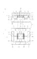
次に、本実施例に係る位置決め装置の位置計測について図1(b)を用いて説明する。図1(b)は図1(a)の拡大図である。支持部材4には、微動ステージ1のX方向位置を計測するためのX干渉計10、Y方向位置を計測するためのY干渉計(不図示)、Z方向位置を計測するためのZ干渉計9a,9bが設けられている。
Next, position measurement of the positioning device according to the present embodiment will be described with reference to FIG. FIG. 1B is an enlarged view of FIG. The support member 4 includes an
粗動ステージ2には、反射面とZ方向のなす角が鋭角(ここでは45°)であるミラー6a,6bが設けられている。ここで、ミラー6a,6bはZ干渉計9a,9bから照射される計測光および参照光をZ方向に反射させる機能を有するものであればよい。また、ミラーは粗動ステージに別途設けられていてもよく、粗動ステージと一体的に設けられていてもよい。
The
微動ステージ1には、XY平面(鉛直方向に垂直な反射面)を有するミラー7a,7bが設けられている。ここで、ミラー7a,7bはミラー6a,6bにより反射された計測光または参照光をさらに反射する機能を有していればよい。
The
支持部材4にも同様に、XY平面(鉛直方向に垂直な反射面)を有するミラー8a,8bが設けられている。ここで、ミラー8a,8bはミラー7a,7bにより反射された計測光または参照光をさらに反射する機能を有していればよい。
Similarly, the support member 4 is provided with
Z干渉計9a(9b)は、参照光と計測光を照射して戻ってきた光を干渉させることによって変位を計測することができるものである。ここで、図1(b)における点線は計測光および参照光の光路を表す。Z干渉計9a(9b)から照射した参照光Laと計測光Lbは、ミラー6a(6b)によってZ方向に折り曲げられる。ここで、参照光Laと計測光Lbがミラー6a(6b)の反射面にあたる位置をそれぞれ異ならせることで、参照光Laはミラー7a(7b)に、計測光Lbはミラー8a(b)に照射するようにする。ミラー7a(7b)、ミラー8a(b)に+Z方向で照射した参照光および計測光はそれぞれ−Z方向で反射されて再びミラー6a(6b)で折り曲げられてZ干渉計9a(9b)に入射する。そして、参照光と計測光を干渉させることで、微動ステージ1と支持部材4との間のZ方向変位dxを計測することができる。
The
ここで、計測光と参照光が導光される光路のうち、水平方向(図ではX方向)の光路dxは、2つとも略同一の空間を通っており、空気揺らぎの影響がキャンセルされるため、計測誤差の低減を図ることができる。 Here, among the optical paths through which the measurement light and the reference light are guided, the two optical paths dx in the horizontal direction (X direction in the figure) pass through substantially the same space, and the influence of the air fluctuation is cancelled. Therefore, it is possible to reduce the measurement error.
なお、計測光Lbを参照光として、参照光Laを計測光としてもよく、お互いを干渉させることによって差分を求めることができればよい。 Note that the measurement light Lb may be used as the reference light and the reference light La may be used as the measurement light, as long as the difference can be obtained by interfering with each other.
X干渉計10からの計測光はミラー6aの側面(YZ平面)によって反射されてX干渉計10に入射する。X干渉計10は計測光と不図示の参照光との差分から微動ステージ1のX方向位置を計測することができる。なお、本実施例ではX方向位置を計測するミラーをZ方向位置を計測するためのミラー6aと兼用させる構成としたが、それぞれ別のミラーを設ける構成としてもよい。
The measurement light from the
Y方向位置の計測についても、XZ平面を有するミラーを微動ステージ1に設け、Y干渉計(不図示)からの計測光を反射させることで、X方向位置と同様に計測することができる。
Regarding the measurement of the Y direction position, a mirror having an XZ plane can be provided on the
また、X干渉計かY干渉計を複数本設けることにより、微動ステージの回転方向(ωx、ωy、ωz方向)の位置を計測することができる。 Further, by providing a plurality of X interferometers or Y interferometers, the position of the fine movement stage in the rotation direction (ωx, ωy, ωz directions) can be measured.
図1(c)は本実施例に係る位置決め装置を+Z方向から見た図である。図のように、ミラー6a,6bおよびミラー7a,7bはY方向に沿って配置されている。これにより、粗動ステージの移動に対してZ干渉計を移動させることなく、干渉計を切らさない構成が可能となる。
FIG.1 (c) is the figure which looked at the positioning apparatus based on a present Example from + Z direction. As illustrated, the
また、ミラー6a,6bを粗動ステージ2の対辺となる位置に設けられ、ミラー7a,7bを微動ステージ1の対辺となる位置に設けられている。これにより、片側のミラー(たとえば、6a,7a)の上方に投影光学系があるときでも、もう片側のミラー(6b,7b)を用いて微動ステージ1のZ方向の位置計測をすることができる。つまり、粗動ステージ2が大きな範囲で移動した場合でも、Z干渉計9aまたは9bの少なくともどちらか一方が微動ステージ1のZ方向の位置計測をすることができ、結果として常にZ方向の位置計測ができる。
Further, the
上述の構成では、ミラー8の反射面を支持部材4の下面全域に設ける必要がなく、ミラー8a,8bはミラー6a,6bおよびミラー7a,7bに対して垂直な方向(X方向)に沿って、投影光学系20を通る直線上に分割して配置されている。この場合、精度の必要なミラー面積が小さくてすむため、精度の向上またはコストの低減を図ることができる。
In the above-described configuration, it is not necessary to provide the reflecting surface of the mirror 8 over the entire lower surface of the support member 4, and the
ここで、Z干渉計の計測光9a,9bはミラー8a,8bの下方でミラー6a,6bにX方向から照射されるように導光されていればよい。
Here, the
なお、ミラー6a,6bおよびミラー7a,7bをX方向に沿って配置し、ミラー8a,8bをY方向に沿って配置し、Z干渉計がミラー6a,6bに対してY方向から照射するように配置することも可能である。
The
(変形例)
上述の説明では、粗動ステージ2は平面モータによって駆動していたが、これに限られるものではなく、さまざまな駆動機構が考えられる。
(Modification)
In the above description, the
変形例として、図2ではガイドを用いたリニアモータによって粗動ステージ2を駆動させている。リニアモータ固定子17X、17Yが定盤5に設けられており、リニアモータ可動子18Xはリニアモータ固定子17Xに対してX方向に移動し、リニアモータ可動子18Yはリニアモータ固定子17Yに対してY方向に移動する。リニアモータ可動子18X、18Yは粗動ステージ2を貫通するように設けられており、リニアモータ可動子18X、18Yが移動することで粗動ステージ2はXY方向に大きな範囲で移動することができる。
As a modification, in FIG. 2, the
なお、本実施例において、位置決め装置は露光装置に適用されているが、そのほかの工作機器においても適用が可能である。 In the present embodiment, the positioning device is applied to the exposure apparatus, but it can also be applied to other machine tools.
(実施例2)
図3を用いて実施例2に係る位置決め装置について説明する。実施例2についても位置決め装置を露光装置に適用した例を示す。図中で実施例1と同様の機能を有する構成要素については同一の番号を付して詳細な説明を省略する。
(Example 2)
A positioning apparatus according to the second embodiment will be described with reference to FIG. Example 2 also shows an example in which the positioning device is applied to an exposure apparatus. In the figure, components having the same functions as those in the first embodiment are denoted by the same reference numerals, and detailed description thereof is omitted.
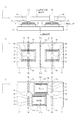
実施例2は粗動ステージと微動ステージ(以下、まとめて粗微動ステージと称する)が2つずつ設けられている点が大きく異なる。このような位置決め装置は、近年、露光装置において特に注目されており、片方の粗微動ステージ上のウエハに露光している間に、他方の粗微動ステージ上のウエハのアライメントをすることが可能となるため、スループットの向上が期待できる。ここで、アライメントとは、ウエハ内の各チップのXY方向の位置合わせや、各チップのZ方向の位置合わせを含むものである。 The second embodiment is greatly different in that two coarse movement stages and two fine movement stages (hereinafter collectively referred to as coarse / fine movement stages) are provided. In recent years, such a positioning device has attracted particular attention in an exposure apparatus, and it is possible to align a wafer on the other coarse / fine movement stage while exposing the wafer on one coarse / fine movement stage. Therefore, improvement in throughput can be expected. Here, the alignment includes alignment of each chip in the wafer in the XY direction and alignment of each chip in the Z direction.
図3において、20は投影光学系、30はアライメント光学系であり、これらを支持部材4が支持する。粗動ステージを案内する定盤は露光領域13と計測領域12に分割されている。ここで、露光領域は、投影光学系20の下方に位置し、微動ステージ上のウエハに露光する際に粗微動ステージが定盤上を移動する領域として定義される。また、計測領域はアライメント光学系の下方に位置し、微動ステージ上のウエハのアライメントを行う際に粗微動ステージが定盤上を移動する領域として定義される。
In FIG. 3, 20 is a projection optical system, and 30 is an alignment optical system, and these are supported by the support member 4. The surface plate for guiding the coarse movement stage is divided into an
粗動ステージ21にはミラー6a,6bが、粗動ステージ22にはミラー6c,6dが設けられている。また、微動ステージ11にはミラー7a,7bが、微動ステージ12にはミラー7c,7dが設けられている。ミラー8は投影光学系20とアライメント光学系30を結ぶ直線に対して垂直な方向(図においてX方向)に沿って配置されており、ミラー8a,8bは投影光学系を通る直線上、ミラー8c,8dはアライメント光学系を通る直線上に配置されている。
The
このように、ミラー8を投影光学系とアライメント光学系を結ぶ直線に対して垂直な方向に沿って配置させることで、露光または計測の動作中にZ位置計測に用いる計測光および参照光が他方の粗微動ステージにさえぎられないようにしている。 In this way, by arranging the mirror 8 along a direction perpendicular to the straight line connecting the projection optical system and the alignment optical system, the measurement light and the reference light used for the Z position measurement during the exposure or measurement operation are the other. Is not interrupted by the coarse and fine movement stage.
なお、ミラー6a〜6d、7a〜7d,8a〜8dの機能については、実施例1と同様であるので説明を省略する。
Since the functions of the
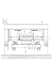
次に、図3(c)を用いて露光領域13と計測領域12間での2つの粗微動ステージ入れ換え(スワップ)について説明する。露光領域でウエハの露光を終えた粗微動ステージ(11,21)は、不図示の搬入出位置へ移動して露光済のウエハを搬出し、新たなウエハを搬入して、アライメントをするために計測領域12へと移動する。また、他方の粗微動ステージ(22,22)はアライメントを終えたウエハの露光をするために露光領域13へと移動する。このような動作を繰り返して複数枚のウエハに対してアライメント処理と露光処理を行う。
Next, replacement of two coarse / fine movement stages (swap) between the
支持部材4にはXY平面(鉛直方向に垂直な反射面)を有するミラー16a,16bが設けられており、露光領域と計測領域との間に配置されている。また、Z干渉計15a,15bが、ミラー16a,16bの下方でX方向両側から計測光および参照光を照射するように配置されている。
The support member 4 is provided with
ここで、Z干渉計15a(15b)から照射された計測光および参照光は、図3(c)のように2つの粗微動ステージの入れ替えが行われる際、ミラー6a(6d)によってZ方向に折り曲げられる。ここで、計測光と参照光がミラー6a(6d)の反射面にあたる位置をそれぞれ異ならせることで、参照光はミラー7a(7d)に、計測光はミラー16a(16b)に照射するようにする。ミラー7a(7d)、ミラー16a(16b)に+Z方向で照射した計測光および参照光はそれぞれ−Z方向で反射されて再びミラー6a(6d)で折り曲げられてZ干渉計15a(15d)に入射する。そして、参照光と計測光を干渉させることで、微動ステージ11(21)と支持部材4との間のZ方向変位を計測することができる。
Here, the measurement light and the reference light emitted from the Z interferometer 15a (15b) are moved in the Z direction by the
ここで、計測光と参照光が導光される光路のうち、水平方向(図ではX方向)の光路dxは、2つとも略同一の空間を通っており、空気揺らぎの影響がキャンセルされるため、計測誤差の低減を図ることができる。 Here, among the optical paths through which the measurement light and the reference light are guided, the two optical paths dx in the horizontal direction (X direction in the figure) pass through substantially the same space, and the influence of the air fluctuation is cancelled. Therefore, it is possible to reduce the measurement error.
さらに、ミラー6およびミラー7のY方向における長さよりも、Z干渉計9からの計測光がミラー6に照射する位置とZ干渉計15からの計測光がミラー6に照射する位置との間のY方向における距離を短くすることで、ステージ入れ換え時における微動ステージ1のZ方向位置を引き継いで計測することができる。
Furthermore, the distance between the position where the measurement light from the Z interferometer 9 irradiates the
このように、2つの粗微動ステージがすれ違う位置(露光領域と計測領域との間)の鉛直上方にミラー16を設けることで、2つの粗微動ステージの入れ換えの際にも常にZ方向の位置計測を行うことができる。 In this way, by providing the mirror 16 vertically above the position where the two coarse / fine movement stages pass (between the exposure area and the measurement area), the position measurement in the Z direction is always performed even when the two coarse / fine movement stages are interchanged. It can be performed.
なお、本実施例では定盤が露光領域12と計測領域13に分割されているため、各領域における熱の影響と振動の影響を遮断でき、相互の干渉を低減できる。このような定盤が分割された構成では、ステージ入れ換え時におけるZ方向位置の補償が重要となるため、本実施例における効果はより顕著となる。
In the present embodiment, since the surface plate is divided into the
実施例1および実施例2において、位置決め装置が露光装置のウエハステージに用いられることによって、高精度または高スループットな露光装置を提供することができる。また、このような露光装置を用いて製造するデバイス製造方法を以下において説明する。 In the first and second embodiments, the positioning apparatus is used for the wafer stage of the exposure apparatus, so that an exposure apparatus with high accuracy or high throughput can be provided. A device manufacturing method manufactured using such an exposure apparatus will be described below.
(露光装置を用いたデバイス製造方法)
次に、この露光装置を利用した半導体デバイスの製造プロセスを説明する。図4は半導体デバイスの全体的な製造プロセスのフローを示す図である。ステップ1(回路設計)では半導体デバイスの回路設計を行う。ステップ2(マスク作製)では設計した回路パターンに基づいてマスクを作製する。
(Device manufacturing method using exposure apparatus)
Next, a semiconductor device manufacturing process using this exposure apparatus will be described. FIG. 4 is a flowchart showing the overall manufacturing process of the semiconductor device. In step 1 (circuit design), a semiconductor device circuit is designed. In step 2 (mask fabrication), a mask is fabricated based on the designed circuit pattern.
一方、ステップ3(ウエハ製造)ではシリコン等の材料を用いてウエハを製造する。ステップ4(ウエハプロセス)は前工程と呼ばれ、上記のマスクとウエハを用いて、上記の露光装置によりリソグラフィ技術を利用してウエハ上に実際の回路を形成する。次のステップ5(組み立て)は後工程と呼ばれ、ステップ5によって作製されたウエハを用いて半導体チップ化する工程であり、アッセンブリ工程(ダイシング、ボンディング)、パッケージング工程(チップ封入)等の組み立て工程を含む。ステップ6(検査)ではステップ5で作製された半導体デバイスの動作確認テスト、耐久性テスト等の検査を行う。こうした工程を経て半導体デバイスが完成し、ステップ7でこれを出荷する。 On the other hand, in step 3 (wafer manufacture), a wafer is manufactured using a material such as silicon. Step 4 (wafer process) is called a pre-process, and an actual circuit is formed on the wafer by using the above-described exposure apparatus and lithography technology using the above-described mask and wafer. The next step 5 (assembly) is called a post-process, which is a process for forming a semiconductor chip using the wafer produced in step 5, and is an assembly process (dicing, bonding), packaging process (chip encapsulation), etc. Process. In step 6 (inspection), the semiconductor device manufactured in step 5 undergoes inspections such as an operation confirmation test and a durability test. A semiconductor device is completed through these processes, and is shipped in Step 7.
上記ステップ4のウエハプロセスは以下のステップを有する(図5)。ウエハの表面を酸化させる酸化ステップ、ウエハ表面に絶縁膜を成膜するCVDステップ、ウエハ上に電極を蒸着によって形成する電極形成ステップ、ウエハにイオンを打ち込むイオン打ち込みステップ、ウエハに感光剤を塗布するレジスト処理ステップ、上記の露光装置によって回路パターンをレジスト処理ステップ後のウエハに転写する露光ステップ、露光ステップで露光したウエハを現像する現像ステップ、現像ステップで現像したレジスト像以外の部分を削り取るエッチングステップ、エッチングが済んで不要となったレジストを取り除くレジスト剥離ステップ。これらのステップを繰り返し行うことによって、ウエハ上に多重に回路パターンを形成する。 The wafer process in Step 4 has the following steps (FIG. 5). An oxidation step for oxidizing the surface of the wafer, a CVD step for forming an insulating film on the wafer surface, an electrode formation step for forming electrodes on the wafer by vapor deposition, an ion implantation step for implanting ions on the wafer, and applying a photosensitive agent to the wafer A resist processing step, an exposure step for transferring the circuit pattern to the wafer after the resist processing step by the above exposure apparatus, a development step for developing the wafer exposed in the exposure step, and an etching step for scraping off portions other than the resist image developed in the development step A resist stripping step that removes the resist that has become unnecessary after etching. By repeating these steps, multiple circuit patterns are formed on the wafer.
このように、実施例1および実施例2に記載の位置決め装置をウエハステージとして用いた露光装置によってデバイスを製造することで、安価または微細なデバイスを提供することができる。 Thus, by manufacturing a device with an exposure apparatus using the positioning apparatus described in the first and second embodiments as a wafer stage, an inexpensive or fine device can be provided.
1,11,12 微動ステージ
2,21,22 平面粗動ステージ
3 微動アクチュエータ
4 支持部材
5 定盤
6a,6b,7a,7b,8a,8b,16a,16b ミラー
9a,9b,15a,15b Z干渉計
10 X干渉計
14 遮断部材
17 粗動アクチュエータ固定子
18 可動子
20 投影光学系
30 アライメント光学系
40 レチクル
50 照明系
51 露光領域(定盤)
52 計測領域(定盤)
1, 11, 12
52 Measurement area (surface plate)
Claims (9)
前記粗動ステージに設けられ、水平方向に照射される光を鉛直方向に反射する反射面を有する第1ミラーと、前記微動ステージに設けられ、水平方向に平行な反射面を有する第2ミラーと、
前記微動ステージの鉛直方向位置を計測する際の基準である基準構造体と、
該基準構造体に設けられ、水平方向に平行な反射面を有する第3ミラーと、
前記第1のミラーによって反射された参照光と計測光をそれぞれ前記第2ミラーと前記第3ミラーに反射させることによって前記微動ステージの鉛直方向位置を計測するための干渉計とを有することを特徴とする位置決め装置。 A positioning device having a coarse movement stage and a fine movement stage,
A first mirror provided on the coarse movement stage and having a reflection surface that reflects light irradiated in the horizontal direction in the vertical direction; and a second mirror provided on the fine movement stage and having a reflection surface parallel to the horizontal direction ; ,
A reference structure which is a reference when measuring the vertical position of the fine movement stage;
A third mirror provided on the reference structure and having a reflecting surface parallel to the horizontal direction ;
An interferometer for measuring the vertical position of the fine movement stage by reflecting the reference light and measurement light reflected by the first mirror to the second mirror and the third mirror, respectively. Positioning device.
一方の微動ステージ上の基板に露光するための投影光学系と、
一方の微動ステージ上の基板に露光している間に他方の微動ステージ上の基板の位置合わせができるように配置されたアライメント光学系とを有し、
前記第3ミラーは前記投影光学系とアライメント光学系とを結ぶ線分と垂直な方向に沿って設けられることを特徴とする露光装置。 An exposure apparatus having two positioning devices according to claim 1,
A projection optical system for exposing the substrate on one fine movement stage;
An alignment optical system arranged so that the substrate on the other fine movement stage can be aligned while exposing the substrate on one fine movement stage;
The exposure apparatus according to claim 1, wherein the third mirror is provided along a direction perpendicular to a line segment connecting the projection optical system and the alignment optical system.
前記基準構造体には、入れ換えの際に2つの位置決め装置がすれ違う位置に、反射面が鉛直方向に対して垂直である第4ミラーが設けられていることを特徴とする請求項6に記載の露光装置。 The two positioning devices are interchangeable between a lower part of the projection optical system and a lower part of the alignment optical system,
The said reference structure is provided with the 4th mirror with which a reflective surface is perpendicular | vertical with respect to a perpendicular direction in the position where two positioning devices pass at the time of replacement. Exposure device.
Priority Applications (4)
| Application Number | Priority Date | Filing Date | Title |
|---|---|---|---|
| JP2004196455A JP4262153B2 (en) | 2004-07-02 | 2004-07-02 | Positioning apparatus and exposure apparatus using the same |
| US11/157,781 US7193723B2 (en) | 2004-07-02 | 2005-06-21 | Positioning apparatus and photolithography apparatus including the same |
| EP05254122A EP1612608A3 (en) | 2004-07-02 | 2005-06-30 | Positioning apparatus and photolithography apparatus including the same |
| KR1020050058982A KR100658572B1 (en) | 2004-07-02 | 2005-07-01 | Positioning apparatus and photolithography apparatus including the same |
Applications Claiming Priority (1)
| Application Number | Priority Date | Filing Date | Title |
|---|---|---|---|
| JP2004196455A JP4262153B2 (en) | 2004-07-02 | 2004-07-02 | Positioning apparatus and exposure apparatus using the same |
Publications (3)
| Publication Number | Publication Date |
|---|---|
| JP2006019549A JP2006019549A (en) | 2006-01-19 |
| JP2006019549A5 JP2006019549A5 (en) | 2007-08-16 |
| JP4262153B2 true JP4262153B2 (en) | 2009-05-13 |
Family
ID=34941792
Family Applications (1)
| Application Number | Title | Priority Date | Filing Date |
|---|---|---|---|
| JP2004196455A Expired - Fee Related JP4262153B2 (en) | 2004-07-02 | 2004-07-02 | Positioning apparatus and exposure apparatus using the same |
Country Status (4)
| Country | Link |
|---|---|
| US (1) | US7193723B2 (en) |
| EP (1) | EP1612608A3 (en) |
| JP (1) | JP4262153B2 (en) |
| KR (1) | KR100658572B1 (en) |
Families Citing this family (5)
| Publication number | Priority date | Publication date | Assignee | Title |
|---|---|---|---|---|
| DE102009025977A1 (en) | 2009-06-16 | 2010-12-23 | Q-Cells Se | Solar cell and manufacturing process of a solar cell |
| DE102011006055A1 (en) * | 2011-03-24 | 2012-09-27 | Carl Zeiss Smt Gmbh | Position measuring device for mask inspection device for inspecting lithographic mask of arrangement of a positioning system, is configured by location or tilted position or certain position of object |
| CN102998913B (en) * | 2012-12-27 | 2015-02-04 | 苏州大学 | Simultaneous localization photoetching exposure device and method |
| CN103309177B (en) * | 2013-06-19 | 2015-02-11 | 清华大学 | Workpiece platform system of photoetching machine |
| CN112113509B (en) * | 2019-06-20 | 2022-06-17 | 上海微电子装备(集团)股份有限公司 | Gantry type measuring device and gantry type measuring method |
Family Cites Families (10)
| Publication number | Priority date | Publication date | Assignee | Title |
|---|---|---|---|---|
| JP3531894B2 (en) * | 1996-09-13 | 2004-05-31 | キヤノン株式会社 | Projection exposure equipment |
| US6020964A (en) * | 1997-12-02 | 2000-02-01 | Asm Lithography B.V. | Interferometer system and lithograph apparatus including an interferometer system |
| JP3630964B2 (en) | 1997-12-26 | 2005-03-23 | キヤノン株式会社 | Stage apparatus, exposure apparatus using the same, and device manufacturing method |
| JP2000049066A (en) * | 1998-07-27 | 2000-02-18 | Canon Inc | Aligner and manufacture of devices |
| US6160628A (en) * | 1999-06-29 | 2000-12-12 | Nikon Corporation | Interferometer system and method for lens column alignment |
| JP2001160535A (en) | 1999-09-20 | 2001-06-12 | Nikon Corp | Aligner and device manufacturing using the same |
| JP2001143997A (en) | 1999-11-15 | 2001-05-25 | Canon Inc | Positioning apparatus, aligner, and device manufacturing method |
| JP3762307B2 (en) | 2001-02-15 | 2006-04-05 | キヤノン株式会社 | Exposure apparatus including laser interferometer system |
| JP2003123832A (en) | 2001-10-11 | 2003-04-25 | Nec Tokin Corp | Laminate film-covered battery device and production process thereof |
| US7443511B2 (en) * | 2003-11-25 | 2008-10-28 | Asml Netherlands B.V. | Integrated plane mirror and differential plane mirror interferometer system |
-
2004
- 2004-07-02 JP JP2004196455A patent/JP4262153B2/en not_active Expired - Fee Related
-
2005
- 2005-06-21 US US11/157,781 patent/US7193723B2/en not_active Expired - Fee Related
- 2005-06-30 EP EP05254122A patent/EP1612608A3/en not_active Withdrawn
- 2005-07-01 KR KR1020050058982A patent/KR100658572B1/en not_active IP Right Cessation
Also Published As
| Publication number | Publication date |
|---|---|
| KR20060049732A (en) | 2006-05-19 |
| EP1612608A2 (en) | 2006-01-04 |
| US20060001889A1 (en) | 2006-01-05 |
| US7193723B2 (en) | 2007-03-20 |
| EP1612608A3 (en) | 2007-10-31 |
| KR100658572B1 (en) | 2006-12-19 |
| JP2006019549A (en) | 2006-01-19 |
Similar Documents
| Publication | Publication Date | Title |
|---|---|---|
| JP6566389B2 (en) | Exposure apparatus, exposure method, and device manufacturing method | |
| EP2466383B1 (en) | Wafer table for immersion lithography | |
| US8009275B2 (en) | Movable stage apparatus | |
| US20060098184A1 (en) | Stage apparatus, fixation method, exposure apparatus, exposure method, and device-producing method | |
| US20060175993A1 (en) | Alignment apparatus, exposure apparatus, and device manufacturing method | |
| US7907256B2 (en) | Stage apparatus, exposure apparatus, and method for manufacturing device | |
| KR20190131146A (en) | Object processing apparatus, exposure apparatus and exposure method, and device manufacturing method | |
| JP2005317916A (en) | Exposure apparatus and device manufacturing method | |
| KR100658572B1 (en) | Positioning apparatus and photolithography apparatus including the same | |
| KR20120031076A (en) | Movable body apparatus, exposure apparatus and device manufacturing method | |
| JP5455166B2 (en) | Exposure method, exposure apparatus, and device manufacturing method | |
| US7733462B2 (en) | Exposure apparatus and exposure method | |
| JPWO2004075268A1 (en) | Moving method, exposure method, exposure apparatus, and device manufacturing method | |
| JP4630567B2 (en) | Exposure apparatus and device manufacturing method | |
| JP2008147411A (en) | Aligner, and device manufacturing method | |
| WO2014136143A1 (en) | Mobile device, exposure device, and device production method | |
| JP2007335476A (en) | Exposure apparatus and device manufacturing method | |
| JP5757397B2 (en) | Exposure method, exposure apparatus, and device manufacturing method | |
| JP2009038258A (en) | Aligner, and device manufacturing method | |
| JP2012089768A (en) | Exposure device and device manufacturing method |
Legal Events
| Date | Code | Title | Description |
|---|---|---|---|
| A521 | Request for written amendment filed |
Free format text: JAPANESE INTERMEDIATE CODE: A523 Effective date: 20070702 |
|
| A621 | Written request for application examination |
Free format text: JAPANESE INTERMEDIATE CODE: A621 Effective date: 20070702 |
|
| A977 | Report on retrieval |
Free format text: JAPANESE INTERMEDIATE CODE: A971007 Effective date: 20080515 |
|
| A131 | Notification of reasons for refusal |
Free format text: JAPANESE INTERMEDIATE CODE: A131 Effective date: 20080520 |
|
| A521 | Request for written amendment filed |
Free format text: JAPANESE INTERMEDIATE CODE: A523 Effective date: 20080717 |
|
| TRDD | Decision of grant or rejection written | ||
| A01 | Written decision to grant a patent or to grant a registration (utility model) |
Free format text: JAPANESE INTERMEDIATE CODE: A01 Effective date: 20090120 |
|
| A01 | Written decision to grant a patent or to grant a registration (utility model) |
Free format text: JAPANESE INTERMEDIATE CODE: A01 |
|
| A61 | First payment of annual fees (during grant procedure) |
Free format text: JAPANESE INTERMEDIATE CODE: A61 Effective date: 20090206 |
|
| FPAY | Renewal fee payment (event date is renewal date of database) |
Free format text: PAYMENT UNTIL: 20120220 Year of fee payment: 3 |
|
| R150 | Certificate of patent or registration of utility model |
Free format text: JAPANESE INTERMEDIATE CODE: R150 |
|
| FPAY | Renewal fee payment (event date is renewal date of database) |
Free format text: PAYMENT UNTIL: 20130220 Year of fee payment: 4 |
|
| FPAY | Renewal fee payment (event date is renewal date of database) |
Free format text: PAYMENT UNTIL: 20140220 Year of fee payment: 5 |
|
| LAPS | Cancellation because of no payment of annual fees |