JP4260344B2 - Spectrum analyzer - Google Patents
Spectrum analyzer Download PDFInfo
- Publication number
- JP4260344B2 JP4260344B2 JP2000196715A JP2000196715A JP4260344B2 JP 4260344 B2 JP4260344 B2 JP 4260344B2 JP 2000196715 A JP2000196715 A JP 2000196715A JP 2000196715 A JP2000196715 A JP 2000196715A JP 4260344 B2 JP4260344 B2 JP 4260344B2
- Authority
- JP
- Japan
- Prior art keywords
- peak value
- signal
- value
- converter
- negative peak
- Prior art date
- Legal status (The legal status is an assumption and is not a legal conclusion. Google has not performed a legal analysis and makes no representation as to the accuracy of the status listed.)
- Expired - Fee Related
Links
Images


Landscapes
- Measurement Of Current Or Voltage (AREA)
Description
【0001】
【発明の属する技術分野】
本発明は、スペクトラムアナライザに関し、特に、ネガティブピーク値、ポジティブピーク値及びそれらの平均値を選択的に又は同時に表示することができるスペクトラムアナライザに関する。
【0002】
【従来の技術】
従来、スペクトラムアナライザは測定期間中の最大値(ポジティブピーク)の平均値、最小値(ネガティブピーク)の平均値の一方もしくは双方を選択して変換することができ、解析の信号に最も適した変換モードを選択して解析するようになっている。
【0003】
これら信号のピーク値は、大別して2種の方法によって得ることができる。
1.スペクトラムアナライザに設けられるVBWフィルタの帯域(ビデオ信号の帯域)を狭くしてビデオアベレージをとる方法。
2.信号を所定Nサンプリング時に複数サンプリング後にこれらを平均化して得る方法。
【0004】
【発明が解決しようとする課題】
上記1.の方法では、1回のサンプリングで平均値を得ることができるが、装置のハード的制約により応答時間がかかり、測定時間がかかる問題があった。これによりビデオアベレージの高速化を図ることができなかった。
2.の方法では、所定周期毎のサンプリング時の値を用いるため、信号のピーク値を得ることができないとともに、複数画面のサンプリングを平均化するため、例えば1画面に1sec かかると10画面の平均では10sec かかり、処理時間がかかった。
【0005】
また、上記1.2.いずれの構成においても、ポジティブピークの平均値、あるいはネガティブピークの平均値のいずれか一方または、ピークホールドしていない波形の平均値のみしか得ることができず、これらポジティブピークとネガティブピーク間の平均値を得ることはできなかった。
これにより、信号の種類によって様々な観点から解析を行う際に、ネガティブピークとポジティブピークの波形の平均値が必要な場合であってもこれが行えなかった。
【0006】
本発明は、上記課題を解決するためになされたものであり、特に、ポジティブピークとネガティブピークの平均値を装置への処理負担を掛けずに得て表示できるスペクトラムアナライザの提供を目的としている。
【0007】
【課題を解決するための手段】
上記目的を達成するため、本発明の請求項1に係るスペクトラムアナライザは、被測定信号を所定周期で周波数掃引して中間周波数信号に変換して出力する受信部(6)と、
前記中間周波数信号を受けて、被測定信号のポジティブピーク値及びネガティブピーク値を検出して出力するとともにクロックでリセットされる検波部(18)と、
前記所定周期内に所定サンプリング数m(2以上の整数)で前記検波部の出力を前記クロックに同期してサンプリングしてデジタルデータに変換して出力するA/D変換部(19)と、
前記所定周期内のデジタルデータをk(1以上前記m以下の整数)個のサンプリング数分受ける毎に前記ポジティブピーク値とネガティブピーク値との平均値を求めて出力する信号処理部(21)と、
前記信号処理部の出力を受けて前記被測定信号のスペクトラム波形として表示する表示部(17)と、
を備え、
前記表示部は、1回の前記周波数掃引当たりN個の表示ポイント数のデータで表わされる前記スペクトラム波形を表示し、
前記A/D変換部(19)は、1回の前記周波数掃引当たり、前記所定サンプリング数mが前記N個の前記k倍となるm=kN回の前記サンプリングを行い、
前記信号処理部(21)は、前記k個のサンプリング数のデジタルデータを平均して1つの前記表示ポイントのデータとして前記平均値を求め、
さらに、前記表示部は、前記信号処理部から前記平均値を受ける毎に前記スペクトラム波形の表示を更新することを特徴とする。
【0009】
また、本発明の請求項2に係るスペクトラムアナライザは、被測定信号を所定周期で周波数掃引して中間周波数信号に変換して出力する受信部(6)と、
前記中間周波数信号を受けて、被測定信号のポジティブピーク値及びネガティブピーク値を検出して出力するとともにクロックでリセットされる検波部(18)と、
前記所定周期内に所定サンプリング数m(2以上の整数)で前記検波部の出力を前記クロックに同期してサンプリングしてデジタルデータに変換して出力するA/D変換部(19)と、
前記所定周期内のデジタルデータを受けて、前記ポジティブピーク値とネガティブピーク値との平均値を求めて出力する信号処理部(21)と、
前記信号処理部の出力を受けて前記被測定信号のスペクトラム波形として表示する表示部(17)と、
を備え、
前記A/D変換部(19)は、1個のA/D変換器を有し、前記検波部(18)が検出した被測定信号のポジティブピーク値又はネガティブピーク値を交互に前記クロック毎に切り替えてデジタルデータに変換し、
前記信号処理部(21)は、前記A/D変換部から交互に変換されたポジティブピーク値とネガティブピーク値とを取り込み、h(2以上前記m以下の整数)個のサンプリング数毎にポジティブピーク値とネガティブピーク値との平均値を求め、
前記表示部は、前記信号処理部から前記平均値を受ける毎に前記スペクトラム波形の表示を更新することを特徴とする。
【0010】
また、上記請求項1に係るスペクトラムアナライザにおいて、
前記検波部(18)は、前記被測定信号の入力信号経路に対し互いに並列接続されたポジティブピーク検出回路(26)及びネガティブピーク検出回路(27)と、
前記ポジティブピーク検出回路及びネガティブピーク検出回路にそれぞれ設けられ各検出したピーク値を保持する保持回路とを有し、
前記A/D変換部(19)は、前記ポジティブピーク検出回路とネガティブピーク検出回路の出力をそれぞれ独立してA/D変換する構成としてもよい。
【0011】
上記構成によれば、入力される被測定信号のポジティブピーク値とネガティブピーク値が検出される。また、これらポジティブピーク値とネガティブピーク値との平均値が算出される。表示部上にはポジティブピーク値、ネガティブピーク値、これらの平均値のスペクトラム波形が選択的、あるいは同時に波形表示される。
【0012】
【発明の実施の形態】
(第1実施形態)
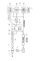
図1は本発明によるスペクトラムアナライザの概略構成を示すブロック図である。以下、図1を参照しながら本例のスペクトラムアナライザ1の構成を、その信号処理手順に沿って説明する。
【0013】
入力端子2を介して入力される例えば数百KHz〜数GHzの高周波のアナログの被測定信号は、その信号レベルが減衰器(不図示)により規定レベルに調整されて信号混合器6に入力され、IFフィルタ7を介して出力される。高周波の被測定信号は信号混合器6で局部発振器5からの局部発振信号と合成して中間周波数を有する中間周波数信号に変換されIFフィルタ7で帯域制限された後、LOG変換部15で対数変換された後、VBWフィルタ16に入力される。
【0014】
掃引制御部12には、ユーザによって1掃引時間が設定入力され、設定された掃引時間で掃引周波数範囲(測定周波数範囲)にわたって掃引が行われる。その結果、信号混合器6から出力される中間周波数信号の周波数も掃引動作に同期して変化することになる。
【0015】
IFフィルタ7は、アナログのバンドパスフィルタで構成され、ユーザの設定によりバンド幅(RBW)が可変設定される。IFフィルタ7では、信号混合器6から入力される中間周波数信号の不要な周波数成分を除き、可変設定されるバンド幅の周波数成分の中間周波数信号のみを通過させ、不図示の増幅器でゲイン調整された後にLOG変換部(LOG)15に入力している。
【0016】
IFフィルタ7から不図示の増幅器を介して入力される中間周波数信号は、LOG変換部15により信号レベルがdB単位に変換されて出力され、DC(直流)成分)に落とされた後、次のアナログのVBWフィルタ16に入力される。VBWフィルタ16では、出力部としての表示部17に最終的に表示される周波数スペクトラム波形の高周波成分(雑音成分)を除去して信号を出力している。
【0017】
そして、VBWフィルタ16から出力された信号は次の検波部(DET)18によって検波される。
検波部18は、信号の最大値を検出するポジティブピーク検出手段18aと、信号の最小値を検出するネガティブピーク検出手段18bとによって構成される。これら検出手段18a、18bには、それぞれ図示しないがピークホールド回路が設けられ、次のクロックでリセットされ次の周期で新たなピーク値を保持する。そして、サンプリング周期に同期したクロック周期の間におけるポジティブピーク値とネガティブピーク値がそれぞれ保持されるようになっている。
【0018】
検波部18によって検波された信号は、次のA/D変換部19によりデジタルデータに変換される。A/D変換部19は、周波数掃引される所定周期内で所定サンプリング数m(2以上の整数)でクロックに同期してサンプリングする。このデジタルデータは、信号処理部21内の波形メモリ20に逐次格納され蓄積される。
そして、出力部としての表示部17は、波形メモリ20の出力を基に、掃引部12の1周波数掃引当たり(又は1所定時間間隔当たり)所定ポイント数(N)のデータを被測定信号の特性として出力表示している。
【0019】
なお、上記A/D変換部19は、表示部17が出力表示する1周波数掃引当たり(又は1所定時間間隔当たり)の所定ポイント数Nのk倍(k=1以上m以下の整数)のポイント数kN(以下、サンプリングポイントという)となるレートで検波部18の出力をサンプリングしてデジタルデータを出力している。そして、このデジタルデータが波形メモリ20に逐次格納される。
【0020】
次のDSP、CPU等で構成される信号処理部21では、波形メモリ20に蓄積されたデジタルデータをもとに表示部17の表示画面上の横軸(時間軸又は周波数軸)における表示データの1ポイント間(以下、表示ポイントという)の掃引時間に相当するデータの実効値を演算している。
すなわち、信号処理部21に設けられる平均化処理部22は、波形メモリ20から出力されるデジタルデータを受けて、複数のサンプリングポイント(k)におけるデジタルデータを平均してその値を新たに1表示ポイントのデータとして求め、1周波数掃引当たり又は1所定時間間隔当たりの所定表示ポイント数(N)のデータを表示部17に出力している。平均化の詳細は後述する。
【0021】
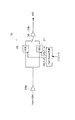
次に、図2は、検波部18を示す回路図である。
VBWフィルタ16からの入力信号は、ポジティブ用検波回路26及びネガティブ用検波回路27にそれぞれ入力される。これら検波回路26,27にはそれぞれピークホールド回路が搭載されており、リセット信号RSTが入力されるまでそれぞれのピーク値を保持し、リセット信号RST入力後には更新したピーク値を保持する。
【0022】
これらポジティブ用検波回路26で保持されたポジティブピーク値と、ネガティブ用検波回路27で保持されたネガティブピーク値はスイッチ28の切替によっていずれか一方が選択的にA/D変換部19に出力される。この検波部18の入出力段にはそれぞれバッファ29a、29bが設けられている。
【0023】
上記スイッチ28は、信号処理部21のクロック発生部23から出力されるクロックに基づき、所定周期で切り替えられる。これにより、リセット信号RSTが入力されるまでの期間中におけるポジティブピーク値あるいはネガティブピーク値が出力される。
ここで、リセット信号RSTは、A/D変換部19のクロックに同期して出力されるが、信号処理部21は、A/D変換部19のクロックの2倍の周期(N逓倍:N=2)でRSTーPあるいはRSTーNを出力する。これにより、検波回路18に入力される信号は、常時、ポジティブ用検波回路26及びネガティブ用検波回路27の双方でピーク検出されるようになっている。
なお、これに同期して波形メモリ20に対する書き込み及び読み出しが行われる。
【0024】
次に、図3のタイムチャートを用いて上記構成の動作を説明する。
検波部18にVBW16から出力される信号波形(a)が入力されると、ポジティブ用検波回路26は、入力信号のポジティブピーク値を検出保持し、ネガティブ用検波回路27は、入力信号のネガティブピーク値を検出保持する。
図3記載のように、これらポジティブ用検波回路26及びネガティブ用検波回路27は、RSTーP、RSTーNのリセット信号が入力される都度、即ち図3(c)記載のDET MODE信号(H:POS、L:NEG)の周期の期間(図中POS、NEGで記載した期間)中におけるポジティブピーク値、及びネガティブピーク値をそれぞれ検出する。これらPOS、NEGの期間は、図示のように、A/D変換部19のクロックを2逓倍した周期であり、常時POSとNEGのピーク値がいずれも検出されるようになっている。
【0025】
そして、A/D変換部19のクロック(同図(b)記載のAD CLOCK)入力毎に、スイッチ28がポジティブ検波回路26とネガティブ検波回路27に交互に切り替えられる。
これにより、同図(a)に示す如く、スイッチ28がポジティブピーク検波回路26に切り替えられると、このA/D変換部19のクロック入力時にそれまでのPOS期間におけるポジティブピーク値(黒丸で示す値)がA/D変換部19に出力される。
次のクロック時には、スイッチ28がネガティブピーク検波回路27に切り替えられ、このクロック入力時にそれまでのNEG期間におけるネガティブピーク値(白丸で示す値)がA/D変換部19に出力される。
【0026】
A/D変換部19はこれら交互に入力されるポジティブピーク値及びネガティブピーク値を所定のサンプリング周期(上記AD CLOCK)でA/D変換し、波形メモリ20の対応する周波数格納エリアに順次格納する。
波形メモリ20には、表示部17に表示される周波数帯域に相当する複数のピーク値(例えば上記所定表示ポイント数N=501個分)が格納され、周波数掃引によって新たなピーク値が取り込まれた際にこの該当する周波数値の波形メモリ20が更新される。
【0027】
平均化処理部22は、交互に取り込まれるポジティブピーク値、及びネガティブピーク値の平均値を求める(POSピーク値の値+NEGピーク値の値)/2。
これにより、POSピーク値が入力されると、直前に取り込んだNEGピーク値との平均値が算出され、該当する周波数部分の平均値として表示部17に表示する(h個のサンプリング数毎に平均が取られることになる。h=2以上m以下の整数)。
この表示更新のタイミングは、図3(d)に示すAD DATAの周期(上記一対のポジティブピーク値及びネガティブピーク値を取得したタイミング)で行われる。
【0028】
これにより、表示部17上には、図4の表示例の如く、所定の周波数範囲でポジティブピーク値とネガティブピーク値(いずれも点線で図示)との平均値(実線)を表示できるようになる。図中横軸方向は上記A/D変換部19の所定クロック(例えば501回)分の周波数範囲、縦軸は各周波数におけるレベルが表示されることになる。
そして、上記構成の装置によれば、上記ポジティブピーク値及びネガティブピーク値の取得単位(POS、NEGの表示書き換え周期)で平均値が算出された周波数部分の表示がリアルタイムに順次更新されていく。
【0029】
また、上記構成の平均化処理部22は、ポジティブピーク値と、ネガティブピーク値を取得した都度、これらの平均値を算出する構成であるため、平均値をリアルタイムに数値表示することが可能となる。
例えば、図4の波形上でマーカーMを設定した箇所におけるポジティブピーク値とネガティブピーク値の平均値を数値表示することができるようになる。
【0030】
(第2実施形態)
上記の第1実施形態では、スイッチ28を用いてA/D変換部19のクロック毎にスイッチを切り替えることにより、単一個のA/D変換部(A/D変換器)19でA/D変換する構成を説明したが、これに限らない。
例えば、図5記載のように、ポジティブピーク検波回路26と、ネガティブピーク検波回路27の後段にそれぞれA/D変換部19a、19bを設ける構成とすれば、スイッチ28を不要にできる。この構成によっても入力信号のポジティブピーク値とネガティブピーク値を同時に検出することができる。
なお、2CH入力を有する単一個のA/D変換器を用いることができることは言うまでもない。
【0031】
上記実施形態では、局部発振器5は、周波数ドメインの状態において、掃引制御部12からの掃引信号により所定の周波数範囲にわたって発振周波数が掃引(周波数掃引)される構成とした、これに対し、タイムドメインの状態では、掃引制御部12からの掃引信号は局部発振器5に送られず、局部発振器5が固定の発振周波数に設定される。この場合、表示部17上には横軸を時間軸とし縦軸を信号のレベルとした波形が表示される事になる。
【0032】
【発明の効果】
本発明によれば、所定周期内のデジタルデータをk(1以上m以下の整数)個のサンプリング数分受ける毎にポジティブピーク値とネガティブピーク値との平均値を信号処理部が求め、表示部が信号処理部から平均値を受ける毎にスペクトラム波形の表示を更新するため、表示部上にリアルタイムで測定した被測定信号のポジティブピークとネガティブピークとの平均値を表示できるようになる。また、簡単な構成で表示上のビデオアベレージの高速化を図ることができるようになる。
また、1個のA/D変換器を用いて被測定信号のポジティブピーク値又はネガティブピーク値を交互にクロック毎に切り替えA/D変換してh(2以上m以下の整数)個のサンプリング数毎にポジティブピーク値とネガティブピーク値との平均値を求める構成とすれば、A/D変換器を最小個数とした簡単な構成であってもほぼリアルタイムで平均値を得ることができるようになる。
さらに、被測定信号の入力信号経路に対し互いに並列接続されたポジティブピーク検出回路及びネガティブピーク検出回路と、ポジティブピーク検出回路及びネガティブピーク検出回路にそれぞれ設けられ各検出したピーク値を保持する保持回路とを検波部が有し、A/D変換部がポジティブピーク検出回路とネガティブピーク検出回路の出力をそれぞれ独立してA/D変換する構成とすれば、並列な2系統で独立してそれぞれピーク値を検出することができ平均値のリアルタイム処理が可能となる。
【図面の簡単な説明】
【図1】本発明のスペクトラムアナライザの実施の形態を示すブロック図。
【図2】検波部の構成を示す回路図。
【図3】装置各部の動作を示すタイミングチャート。
【図4】表示部の表示波形を示す図。
【図5】第2実施形態の構成を示す回路図。
【符号の説明】
1…スペクトラムアナライザ、5…局部発信器、6…信号混合器、7…IFフィルタ、12…掃引制御部、15…LOG変換部、16…VBWフィルタ、17…表示部、18…検波部、18a…ポジティブピーク検出手段、18b…ネガティブピーク検出手段、19(19a,19b)…A/D変換部、20…波形メモリ、21…信号処理部、22…平均化処理部、28…スイッチ。[0001]
BACKGROUND OF THE INVENTION
The present invention relates to a spectrum analyzer, and more particularly to a spectrum analyzer that can selectively or simultaneously display a negative peak value, a positive peak value, and an average value thereof.
[0002]
[Prior art]
Conventionally, a spectrum analyzer can select and convert one or both of the average value of the maximum value (positive peak) and the average value of the minimum value (negative peak) during the measurement period. The mode is selected and analyzed.
[0003]
The peak values of these signals can be roughly obtained by two methods.
1. A method of obtaining video average by narrowing the band (video signal band) of a VBW filter provided in a spectrum analyzer.
2. A method of obtaining a signal by averaging the signals after a plurality of samplings at a predetermined N sampling times.
[0004]
[Problems to be solved by the invention]
Above 1. In this method, although an average value can be obtained by one sampling, there is a problem that it takes a response time and a measurement time due to hardware limitations of the apparatus. As a result, the video average could not be accelerated.
2. In this method, since the value at the time of sampling for each predetermined period is used, the peak value of the signal cannot be obtained and the sampling of a plurality of screens is averaged. For example, if 1 screen takes 1 sec, the average of 10 screens is 10 sec. Took a long time.
[0005]
The above 1.2. In either configuration, only the average value of the positive peak, the average value of the negative peak, or only the average value of the waveform without peak hold can be obtained, and the average between these positive and negative peaks can be obtained. The value could not be obtained.
As a result, when analyzing from various viewpoints depending on the type of signal, this is not possible even when an average value of the waveform of the negative peak and the positive peak is necessary.
[0006]
The present invention has been made to solve the above-described problems, and in particular, it is an object of the present invention to provide a spectrum analyzer that can obtain and display an average value of positive and negative peaks without imposing a processing burden on the apparatus.
[0007]
[Means for Solving the Problems]
In order to achieve the above object, a spectrum analyzer according to claim 1 of the present invention comprises: a receiving unit (6) that sweeps a frequency of a signal under measurement at a predetermined period, converts it into an intermediate frequency signal, and outputs it;
A detector (18) that receives the intermediate frequency signal, detects and outputs a positive peak value and a negative peak value of the signal under measurement, and is reset by a clock;
An A / D converter (19) that samples the output of the detector in synchronization with the clock at a predetermined sampling number m ( an integer of 2 or more ) within the predetermined period, converts the output into digital data, and outputs the digital data;
Wherein the predetermined digital data in the period k (less 1 or the m integer) of the positive peak value for each receive a sampling number of a signal processing unit for outputting an average value of the negative peak value (21) ,
A display unit (17) for receiving the output of the signal processing unit and displaying it as a spectrum waveform of the signal under measurement;
With
The display unit displays the spectrum waveform represented by data of N display points per frequency sweep,
The A / D converter (19) performs the sampling of m = kN times where the predetermined sampling number m is the N times the k times per the frequency sweep,
The signal processing unit (21) averages the digital data of the k sampling numbers to obtain the average value as data of one display point,
Furthermore, the display unit updates the display of the spectrum waveform every time the average value is received from the signal processing unit.
[0009]
Further, the spectrum analyzer according to
A detector (18) that receives the intermediate frequency signal, detects and outputs a positive peak value and a negative peak value of the signal under measurement, and is reset by a clock;
An A / D converter (19) that samples the output of the detector in synchronization with the clock at a predetermined sampling number m (an integer of 2 or more) within the predetermined period, converts the sample into digital data, and outputs the digital data;
A signal processing unit (21) that receives the digital data within the predetermined period, calculates and outputs an average value of the positive peak value and the negative peak value;
A display unit (17) for receiving the output of the signal processing unit and displaying it as a spectrum waveform of the signal under measurement;
With
The A / D converter (19) has one A / D converter, and alternately detects the positive peak value or the negative peak value of the signal under measurement detected by the detector (18) for each clock. Switch to digital data,
The signal processing unit (21), the A / D converter takes in the positive peak value and negative peak value converted alternately from, h (2 or the m an integer) number of positive peaks for each sampling number Find the average of the negative peak value and the value ,
The display unit updates the display of the spectrum waveform every time the average value is received from the signal processing unit .
[0010]
In the spectrum analyzer according to claim 1,
The detector (18) includes a positive peak detection circuit (26) and a negative peak detection circuit (27) connected in parallel to the input signal path of the signal under measurement,
A holding circuit for holding each detected peak value provided in each of the positive peak detection circuit and the negative peak detection circuit;
The A / D converter (19) may be configured to A / D convert the outputs of the positive peak detection circuit and the negative peak detection circuit independently of each other.
[0011]
According to the above configuration, the positive peak value and the negative peak value of the input signal under measurement are detected. The average value of these positive peak value and negative peak value is calculated. On the display section, positive peak values, negative peak values, and spectrum waveforms of these average values are selectively or simultaneously displayed.
[0012]
DETAILED DESCRIPTION OF THE INVENTION
(First embodiment)
FIG. 1 is a block diagram showing a schematic configuration of a spectrum analyzer according to the present invention. Hereinafter, the configuration of the spectrum analyzer 1 of the present example will be described along the signal processing procedure with reference to FIG.
[0013]
For example, a high-frequency analog signal to be measured of several hundred KHz to several GHz input through the
[0014]
One sweep time is set and input to the
[0015]
The
[0016]
The intermediate frequency signal input from the
[0017]
The signal output from the
The
[0018]
The signal detected by the
Based on the output of the
[0019]
The A /
[0020]
In the
That is, the averaging
[0021]
Next, FIG. 2 is a circuit diagram showing the
An input signal from the
[0022]
Either the positive peak value held by the
[0023]
The
Here, the reset signal RST is output in synchronization with the clock of the A /
In synchronization with this, writing to and reading from the
[0024]
Next, the operation of the above configuration will be described using the time chart of FIG.
When the signal waveform (a) output from the
As shown in FIG. 3, the
[0025]
The
As a result, as shown in FIG. 5A, when the
At the next clock, the
[0026]
The A /
The
[0027]
The averaging
Thus, when a POS peak value is input, an average value with the NEG peak value acquired immediately before is calculated and displayed on the
This display update timing is performed in the AD DATA cycle shown in FIG. 3D (the timing at which the pair of positive peak values and negative peak values are acquired).
[0028]
Thus, on the
According to the apparatus having the above-described configuration, the display of the frequency portion in which the average value is calculated in the acquisition unit of the positive peak value and the negative peak value (POS and NEG display rewriting cycle) is sequentially updated in real time.
[0029]
In addition, since the averaging
For example, the average value of the positive peak value and the negative peak value at the location where the marker M is set on the waveform of FIG. 4 can be displayed numerically.
[0030]
(Second Embodiment)
In the first embodiment, the A / D conversion is performed by a single A / D converter (A / D converter) 19 by switching the switch for each clock of the A /
For example, as shown in FIG. 5, if the A /
It goes without saying that a single A / D converter having 2CH inputs can be used.
[0031]
In the above embodiment, the
[0032]
【The invention's effect】
According to the onset bright, the signal processing unit is an average value of the positive peak value and negative peak value for each receive the digital data in a predetermined period k (1 to m integer) sampling a few minutes, the display Since the display of the spectrum waveform is updated every time the unit receives an average value from the signal processing unit, the average value of the positive peak and the negative peak of the signal under measurement measured in real time can be displayed on the display unit. Further, the video average on the display can be increased in speed with a simple configuration .
Also, one A / D converter alternately a positive peak value or negative peak value of the signal to be measured by switching the A / D conversion every clock h (2 or m an integer) by using a number of sampling If the average value of the positive peak value and the negative peak value is obtained for each number, the average value can be obtained almost in real time even with a simple configuration with a minimum number of A / D converters. Become.
Further, the holding which holds the positive peak detecting circuit and a negative peak detection circuit connected in parallel to each other with respect to the input signal path of the signal to be measured, the peak values each detected respectively provided Po Jitibu peak detection circuit and a negative peak detection circuit and a circuit detecting unit, with the configuration of the a / D converter is independently a / D converts the output of the positive peak detecting circuit and a negative peak detector circuit, each independently in parallel two systems The peak value can be detected, and the average value can be processed in real time.
[Brief description of the drawings]
FIG. 1 is a block diagram showing an embodiment of a spectrum analyzer of the present invention.
FIG. 2 is a circuit diagram showing a configuration of a detection unit.
FIG. 3 is a timing chart showing the operation of each part of the apparatus.
FIG. 4 is a diagram showing a display waveform on a display unit.
FIG. 5 is a circuit diagram showing a configuration of a second embodiment.
[Explanation of symbols]
DESCRIPTION OF SYMBOLS 1 ... Spectrum analyzer, 5 ... Local transmitter, 6 ... Signal mixer, 7 ... IF filter, 12 ... Sweep control part, 15 ... LOG conversion part, 16 ... VBW filter, 17 ... Display part, 18 ... Detection part, 18a ... positive peak detection means, 18b ... negative peak detection means, 19 (19a, 19b) ... A / D conversion section, 20 ... waveform memory, 21 ... signal processing section, 22 ... averaging processing section, 28 ... switch.
Claims (3)
前記中間周波数信号を受けて、被測定信号のポジティブピーク値及びネガティブピーク値を検出して出力するとともにクロックでリセットされる検波部(18)と、
前記所定周期内に所定サンプリング数m(2以上の整数)で前記検波部の出力を前記クロックに同期してサンプリングしてデジタルデータに変換して出力するA/D変換部(19)と、
前記所定周期内のデジタルデータをk(1以上前記m以下の整数)個のサンプリング数分受ける毎に前記ポジティブピーク値とネガティブピーク値との平均値を求めて出力する信号処理部(21)と、
前記信号処理部の出力を受けて前記被測定信号のスペクトラム波形として表示する表示部(17)と、
を備え、
前記表示部は、1回の前記周波数掃引当たりN個の表示ポイント数のデータで表わされる前記スペクトラム波形を表示し、
前記A/D変換部(19)は、1回の前記周波数掃引当たり、前記所定サンプリング数mが前記N個の前記k倍となるm=kN回の前記サンプリングを行い、
前記信号処理部(21)は、前記k個のサンプリング数のデジタルデータを平均して1つの前記表示ポイントのデータとして前記平均値を求め、
さらに、前記表示部は、前記信号処理部から前記平均値を受ける毎に前記スペクトラム波形の表示を更新することを特徴とするスペクトラムアナライザ。A receiver (6) for sweeping the frequency of the signal under measurement at a predetermined period, converting it into an intermediate frequency signal, and outputting it;
A detector (18) that receives the intermediate frequency signal, detects and outputs a positive peak value and a negative peak value of the signal under measurement, and is reset by a clock;
An A / D converter (19) that samples the output of the detector in synchronization with the clock at a predetermined sampling number m ( an integer of 2 or more ) within the predetermined period, converts the output into digital data, and outputs the digital data;
Wherein the predetermined digital data in the period k (less 1 or the m integer) of the positive peak value for each receive a sampling number of a signal processing unit for outputting an average value of the negative peak value (21) ,
A display unit (17) for receiving the output of the signal processing unit and displaying it as a spectrum waveform of the signal under measurement;
With
The display unit displays the spectrum waveform represented by data of N display points per frequency sweep,
The A / D converter (19) performs the sampling of m = kN times where the predetermined sampling number m is the N times the k times per the frequency sweep,
The signal processing unit (21) averages the digital data of the k sampling numbers to obtain the average value as data of one display point,
Further, the display unit updates the display of the spectrum waveform every time the average value is received from the signal processing unit.
前記中間周波数信号を受けて、被測定信号のポジティブピーク値及びネガティブピーク値を検出して出力するとともにクロックでリセットされる検波部(18)と、
前記所定周期内に所定サンプリング数m(2以上の整数)で前記検波部の出力を前記クロックに同期してサンプリングしてデジタルデータに変換して出力するA/D変換部(19)と、
前記所定周期内のデジタルデータを受けて、前記ポジティブピーク値とネガティブピーク値との平均値を求めて出力する信号処理部(21)と、
前記信号処理部の出力を受けて前記被測定信号のスペクトラム波形として表示する表示部(17)と、
を備え、
前記A/D変換部(19)は、1個のA/D変換器を有し、前記検波部(18)が検出した被測定信号のポジティブピーク値又はネガティブピーク値を交互に前記クロック毎に切り替えてデジタルデータに変換し、
前記信号処理部(21)は、前記A/D変換部から交互に変換されたポジティブピーク値とネガティブピーク値とを取り込み、h(2以上前記m以下の整数)個のサンプリング数毎にポジティブピーク値とネガティブピーク値との平均値を求め、
前記表示部は、前記信号処理部から前記平均値を受ける毎に前記スペクトラム波形の表示を更新することを特徴とするスペクトラムアナライザ。 A receiver (6) for sweeping the frequency of the signal under measurement at a predetermined period, converting it into an intermediate frequency signal, and outputting it;
A detector (18) that receives the intermediate frequency signal, detects and outputs a positive peak value and a negative peak value of the signal under measurement, and is reset by a clock;
An A / D converter (19) that samples the output of the detector in synchronization with the clock at a predetermined sampling number m (an integer of 2 or more) within the predetermined period, converts the sample into digital data, and outputs the digital data;
A signal processing unit (21) that receives the digital data within the predetermined period, calculates and outputs an average value of the positive peak value and the negative peak value;
A display unit (17) for receiving the output of the signal processing unit and displaying it as a spectrum waveform of the signal under measurement;
With
The A / D converter (19) has one A / D converter, and alternately detects the positive peak value or the negative peak value of the signal under measurement detected by the detector (18) for each clock. Switch to digital data,
The signal processing unit (21), the A / D converter takes in the positive peak value and negative peak value converted alternately from, h (2 or the m an integer) number of positive peaks for each sampling number the average value between the value and the negative peak value,
The spectrum analyzer updates the display of the spectrum waveform every time the average value is received from the signal processing unit .
前記ポジティブピーク検出回路及びネガティブピーク検出回路にそれぞれ設けられ各検出したピーク値を保持する保持回路とを有し、
前記A/D変換部(19)は、前記ポジティブピーク検出回路とネガティブピーク検出回路の出力をそれぞれ独立してA/D変換する請求項1に記載のスペクトラムアナライザ。The detector (18) includes a positive peak detection circuit (26) and a negative peak detection circuit (27) connected in parallel to the input signal path of the signal under measurement,
A holding circuit for holding each detected peak value provided in each of the positive peak detection circuit and the negative peak detection circuit;
The spectrum analyzer according to claim 1, wherein the A / D converter (19) performs A / D conversion on the outputs of the positive peak detection circuit and the negative peak detection circuit independently of each other.
Priority Applications (1)
| Application Number | Priority Date | Filing Date | Title |
|---|---|---|---|
| JP2000196715A JP4260344B2 (en) | 2000-06-29 | 2000-06-29 | Spectrum analyzer |
Applications Claiming Priority (1)
| Application Number | Priority Date | Filing Date | Title |
|---|---|---|---|
| JP2000196715A JP4260344B2 (en) | 2000-06-29 | 2000-06-29 | Spectrum analyzer |
Publications (3)
| Publication Number | Publication Date |
|---|---|
| JP2002014123A JP2002014123A (en) | 2002-01-18 |
| JP2002014123A5 JP2002014123A5 (en) | 2005-07-21 |
| JP4260344B2 true JP4260344B2 (en) | 2009-04-30 |
Family
ID=18695159
Family Applications (1)
| Application Number | Title | Priority Date | Filing Date |
|---|---|---|---|
| JP2000196715A Expired - Fee Related JP4260344B2 (en) | 2000-06-29 | 2000-06-29 | Spectrum analyzer |
Country Status (1)
| Country | Link |
|---|---|
| JP (1) | JP4260344B2 (en) |
Families Citing this family (7)
| Publication number | Priority date | Publication date | Assignee | Title |
|---|---|---|---|---|
| JP5103816B2 (en) * | 2006-07-27 | 2012-12-19 | 株式会社デンソー | Signal processing device |
| WO2008023640A1 (en) * | 2006-08-24 | 2008-02-28 | Advantest Corporation | Spectrum analyzer system and spectrum analyze method |
| JP5220320B2 (en) * | 2007-01-22 | 2013-06-26 | アンリツ株式会社 | Signal analysis apparatus and signal analysis method |
| JPWO2009081780A1 (en) * | 2007-12-20 | 2011-05-06 | 株式会社アドバンテスト | Frequency characteristic measuring device |
| RU2564831C1 (en) * | 2014-04-29 | 2015-10-10 | Федеральное государственное бюджетное образовательное учреждение высшего профессионального образования "Новосибирский государственный технический университет" | Harmonic analyser |
| KR101597649B1 (en) * | 2014-07-01 | 2016-02-25 | 국방과학연구소 | Frequency spectrum display system for detecting frequency hopping signals and method thereof |
| JP2021067598A (en) * | 2019-10-25 | 2021-04-30 | アンリツ株式会社 | Signal analyzer and signal analysis method |
-
2000
- 2000-06-29 JP JP2000196715A patent/JP4260344B2/en not_active Expired - Fee Related
Also Published As
| Publication number | Publication date |
|---|---|
| JP2002014123A (en) | 2002-01-18 |
Similar Documents
| Publication | Publication Date | Title |
|---|---|---|
| US7086083B2 (en) | Noise measurement system | |
| US8179118B2 (en) | Wide-bandwidth spectrum analysis of transient signals using a real-time spectrum analyzer | |
| US5073822A (en) | In-service cable television measurements | |
| US5303262A (en) | Method and apparatus for triggering measurements from a TDMA signal | |
| JPH05196649A (en) | Sampling type signal analyzer | |
| JP2001237701A (en) | Signal analyzing device | |
| KR20060120493A (en) | Rf autocorrelation signal trigger generator | |
| JP4260344B2 (en) | Spectrum analyzer | |
| JP4176479B2 (en) | Frequency analysis method, frequency analysis apparatus, and spectrum analyzer | |
| US20160241253A1 (en) | Two-stage digital down-conversion of rf pulses | |
| US5394185A (en) | In-service CATV HUM measurement technique | |
| US8792542B2 (en) | Method and device for improved detection and analysis of partial discharge activity in and around high voltage electrical equipment | |
| JP2002296310A (en) | Device and method for controlling display of electric power distribution | |
| JP3375919B2 (en) | Signal analyzer | |
| EP0483527A2 (en) | Burst signal spectrum measuring system with stepwise sweeping | |
| JP3900266B2 (en) | Multifunctional measuring system and waveform measuring method | |
| JP4138059B2 (en) | Spectrum analyzer | |
| US6700516B1 (en) | Mixer-based timebase for signal sampling | |
| US6856924B2 (en) | Mixer-based timebase for sampling multiple input signal references asynchronous to each other | |
| JP2001249149A (en) | Signal analyzer | |
| JP2000180484A (en) | Apparatus for measuring harmonic wave | |
| US6310645B1 (en) | Method and apparatus for measuring characteristics of a communication signal modulated with a composite video signal without synchronizing to the signal | |
| JPH10126217A (en) | Decimation filter | |
| JP4074538B2 (en) | Optical sampling device and optical waveform observation system | |
| JP2001313616A (en) | Signal analyzer |
Legal Events
| Date | Code | Title | Description |
|---|---|---|---|
| A521 | Written amendment |
Free format text: JAPANESE INTERMEDIATE CODE: A523 Effective date: 20041129 |
|
| A621 | Written request for application examination |
Free format text: JAPANESE INTERMEDIATE CODE: A621 Effective date: 20041129 |
|
| A977 | Report on retrieval |
Free format text: JAPANESE INTERMEDIATE CODE: A971007 Effective date: 20071001 |
|
| A131 | Notification of reasons for refusal |
Free format text: JAPANESE INTERMEDIATE CODE: A131 Effective date: 20071009 |
|
| A521 | Written amendment |
Free format text: JAPANESE INTERMEDIATE CODE: A523 Effective date: 20071207 |
|
| A131 | Notification of reasons for refusal |
Free format text: JAPANESE INTERMEDIATE CODE: A131 Effective date: 20080415 |
|
| A521 | Written amendment |
Free format text: JAPANESE INTERMEDIATE CODE: A523 Effective date: 20080610 |
|
| TRDD | Decision of grant or rejection written | ||
| A01 | Written decision to grant a patent or to grant a registration (utility model) |
Free format text: JAPANESE INTERMEDIATE CODE: A01 Effective date: 20090113 |
|
| A01 | Written decision to grant a patent or to grant a registration (utility model) |
Free format text: JAPANESE INTERMEDIATE CODE: A01 |
|
| A61 | First payment of annual fees (during grant procedure) |
Free format text: JAPANESE INTERMEDIATE CODE: A61 Effective date: 20090204 |
|
| FPAY | Renewal fee payment (event date is renewal date of database) |
Free format text: PAYMENT UNTIL: 20120220 Year of fee payment: 3 |
|
| R150 | Certificate of patent or registration of utility model |
Free format text: JAPANESE INTERMEDIATE CODE: R150 |
|
| FPAY | Renewal fee payment (event date is renewal date of database) |
Free format text: PAYMENT UNTIL: 20120220 Year of fee payment: 3 |
|
| FPAY | Renewal fee payment (event date is renewal date of database) |
Free format text: PAYMENT UNTIL: 20130220 Year of fee payment: 4 |
|
| FPAY | Renewal fee payment (event date is renewal date of database) |
Free format text: PAYMENT UNTIL: 20140220 Year of fee payment: 5 |
|
| R250 | Receipt of annual fees |
Free format text: JAPANESE INTERMEDIATE CODE: R250 |
|
| R250 | Receipt of annual fees |
Free format text: JAPANESE INTERMEDIATE CODE: R250 |
|
| LAPS | Cancellation because of no payment of annual fees |