JP4255683B2 - Glass wiring board connection structure and display device - Google Patents
Glass wiring board connection structure and display device Download PDFInfo
- Publication number
- JP4255683B2 JP4255683B2 JP2002340076A JP2002340076A JP4255683B2 JP 4255683 B2 JP4255683 B2 JP 4255683B2 JP 2002340076 A JP2002340076 A JP 2002340076A JP 2002340076 A JP2002340076 A JP 2002340076A JP 4255683 B2 JP4255683 B2 JP 4255683B2
- Authority
- JP
- Japan
- Prior art keywords
- wiring
- connection
- substrate
- spare
- side substrate
- Prior art date
- Legal status (The legal status is an assumption and is not a legal conclusion. Google has not performed a legal analysis and makes no representation as to the accuracy of the status listed.)
- Expired - Fee Related
Links
Images


Classifications
-
- G—PHYSICS
- G02—OPTICS
- G02F—OPTICAL DEVICES OR ARRANGEMENTS FOR THE CONTROL OF LIGHT BY MODIFICATION OF THE OPTICAL PROPERTIES OF THE MEDIA OF THE ELEMENTS INVOLVED THEREIN; NON-LINEAR OPTICS; FREQUENCY-CHANGING OF LIGHT; OPTICAL LOGIC ELEMENTS; OPTICAL ANALOGUE/DIGITAL CONVERTERS
- G02F1/00—Devices or arrangements for the control of the intensity, colour, phase, polarisation or direction of light arriving from an independent light source, e.g. switching, gating or modulating; Non-linear optics
- G02F1/01—Devices or arrangements for the control of the intensity, colour, phase, polarisation or direction of light arriving from an independent light source, e.g. switching, gating or modulating; Non-linear optics for the control of the intensity, phase, polarisation or colour
- G02F1/13—Devices or arrangements for the control of the intensity, colour, phase, polarisation or direction of light arriving from an independent light source, e.g. switching, gating or modulating; Non-linear optics for the control of the intensity, phase, polarisation or colour based on liquid crystals, e.g. single liquid crystal display cells
- G02F1/133—Constructional arrangements; Operation of liquid crystal cells; Circuit arrangements
- G02F1/1333—Constructional arrangements; Manufacturing methods
- G02F1/1345—Conductors connecting electrodes to cell terminals
- G02F1/13452—Conductors connecting driver circuitry and terminals of panels
-
- H—ELECTRICITY
- H05—ELECTRIC TECHNIQUES NOT OTHERWISE PROVIDED FOR
- H05K—PRINTED CIRCUITS; CASINGS OR CONSTRUCTIONAL DETAILS OF ELECTRIC APPARATUS; MANUFACTURE OF ASSEMBLAGES OF ELECTRICAL COMPONENTS
- H05K3/00—Apparatus or processes for manufacturing printed circuits
- H05K3/36—Assembling printed circuits with other printed circuits
- H05K3/361—Assembling flexible printed circuits with other printed circuits
-
- H—ELECTRICITY
- H05—ELECTRIC TECHNIQUES NOT OTHERWISE PROVIDED FOR
- H05K—PRINTED CIRCUITS; CASINGS OR CONSTRUCTIONAL DETAILS OF ELECTRIC APPARATUS; MANUFACTURE OF ASSEMBLAGES OF ELECTRICAL COMPONENTS
- H05K2201/00—Indexing scheme relating to printed circuits covered by H05K1/00
- H05K2201/09—Shape and layout
- H05K2201/09209—Shape and layout details of conductors
- H05K2201/09654—Shape and layout details of conductors covering at least two types of conductors provided for in H05K2201/09218 - H05K2201/095
- H05K2201/09781—Dummy conductors, i.e. not used for normal transport of current; Dummy electrodes of components
-
- H—ELECTRICITY
- H05—ELECTRIC TECHNIQUES NOT OTHERWISE PROVIDED FOR
- H05K—PRINTED CIRCUITS; CASINGS OR CONSTRUCTIONAL DETAILS OF ELECTRIC APPARATUS; MANUFACTURE OF ASSEMBLAGES OF ELECTRICAL COMPONENTS
- H05K3/00—Apparatus or processes for manufacturing printed circuits
- H05K3/46—Manufacturing multilayer circuits
- H05K3/4685—Manufacturing of cross-over conductors
Description
【0001】
【発明の属する技術分野】
本発明は、液晶表示装置、有機EL表示装置および無機EL表示装置等のアクティブマトリクス型表示装置において、表示パネルに駆動回路基板を実装する際に用いられる配線基板の接続構造に関するものである。
【0002】
【従来の技術】
現在、液晶表示装置等のアクティブマトリクス型表示装置における表示パネルとこれを駆動する駆動回路との接続は、TCP(Tape Carrier Package)方式、COG(Chip on Glass)方式、低温多結晶シリコン技術を使用したモノリシック方式等が用いられている。
【0003】
TCP方式は、図11に示すように、表示パネル101に対して、ゲート信号線駆動回路となるゲートIC(Integrated Circuit)102を搭載したゲートTCP103およびソース信号線駆動回路となるソースIC104を搭載したソースTCP105が複数接続されている。さらに、上記ゲートTCP103およびソースTCP105は、これらのTCPに信号を入力するためのゲートPWB(Printed Wire Bonding)106およびソースPWB107と接続されている。これらのPWBは、FPC(Flexible Printed Circuit)108によって外部回路基板と接続されている。
【0004】
COG方式は、図12に示すように、表示パネル111にゲート信号線駆動回路となる複数のゲートIC112およびソース信号線駆動回路となる複数のソースIC113が搭載されており、これらのゲートIC112およびソースIC113は、信号を入力するためのゲートFPC114およびソースFPC115と接続され、該ゲートFPC114およびソースFPC115によって外部回路基板と接続される。
【0005】
TCP方式、COG方式は、量産化の実績が長く、製品の品質、信頼性面で有利であるが、部品点数が多く、材料費と実装加工費が高くつくといった問題もある。
【0006】
また、モノリシック方式は、上記COG方式におけるゲートICおよびソースICを低温多結晶技術を応用して表示パネルに作りこんでしまう方式である。この方式は、TCP方式やCOG方式に比べて部品点数を少なくすることができるため、材料費、実装加工費を低減することができる。しかしながら、表示パネル側の設計が複雑になり、このためのコストがアップする。また、表示パネルの大型化には不利であり、使用範囲が限定される。
【0007】
以上の3方式に対して、材料コスト面でモノリシック方式と同等以下で、且つ、表示パネルにTCP方式やCOG方式と同じアモルファスシリコンを使用したGOG(Glass on Glass)方式が、例えば特開平04−283727号公報において考案されている。上記GOG方式では、図13に示すように、FPC124から入力された信号が、表示パネル121上の配線を経由して、駆動回路となるICを搭載したゲートGS(Glass Stick)122およびソースGS123に入力され、表示パネル121を駆動する。
【0008】
上記GOG方式は、モノリシック方式における良品率低下の原因となる駆動回路部分をゲートGS122およびソースGS123として別工程で作成することができるため、歩留まりの低下による表示パネル121のコストアップが低減され、かつTCP方式やCOG方式に比べて部品点数が削減されている。
【0009】
【発明が解決しようとする課題】
ところが、上記従来の構成では、特にTCP方式およびGOG方式において、表示パネルの形成されている基板(以下、表示パネル側基板と称する)と駆動回路となるICの形成されている基板(以下、駆動回路側基板と称する)との接続部に異物かみ込み等の接続異常によるオープン症状やリーク症状が発生する場合がある。そして、このような場合の修正方法においては、以下に示すような問題が生じる。
【0010】
TCP方式における上記接続異常箇所の修正方法では、表示パネル側基板と駆動回路側基板との接続不具合が生じた箇所のTCPを一旦剥離し、パネル表面に残った接続用樹脂の残渣を清掃し、再度、新たなTCPあるいはICを接続する、といった作業が行われる。しかしながら、このような修正方法は、修正作業にかかる工程が多く存在し、作業効率が悪いといった問題がある。
【0011】
また、GOG方式における異物かみ込み等の基板間の接続異常によるオープン症状やリーク症状に対しては、TCP方式と同様の修正方法を適用した場合、作業効率の問題以外に以下のような問題も生じる。すなわち、GOG方式はコスト面で他の方式に比べて有利であるが、GOG接続の異物かみ込みによる不良発生率の増加、および、接続不良が発生した場合のGS交換の難しさが、大きな問題となる。
【0012】
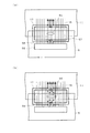
まず、GOG方式における基板接続箇所の異物かみ込みによる不良発生率の増加であるが、図14(a),(b)および図15(a),(b)に基いてこれを説明する。図14(a)は図11のA−A’断面図であり、接続される基板間に異物がかみ込んだ場合を示す。図15(a)は図13のB−B’断面図であり、接続される基板間に異物がかみ込んだ場合を示す。
【0013】
TCP方式の場合は、図14(a)に示すように、異物131がかみ込んだ場所の表示パネル側基板の端子109と駆動回路側基板の端子110は離れてしまっているが、TCP側基板にフレキシブル性があるため、異物131をかみ込んだ端子に隣接した端子では端子同士の接続が確保されている。また、図14(b)に示すように、接続される端子が比較的長い接続領域を有する場合には、異物131をかみ込んだ端子であっても、該異物131から離れた領域では端子間の接続が得られる。
【0014】
これに対し、GOG方式の場合では、図15(a)に示すように、駆動回路側基板にフレキシブル性が無いため、異物131をかみ込んだ箇所で表示パネル側基板の端子125と駆動回路側基板の端子126とがオープン状態となるばかりでなく、隣接した端子もオープン状態となりやすい。また、図15(b)に示すように、接続される端子が比較的長い接続領域を有する場合であっても、異物131から離れた領域でも端子間の接続が得られない。
【0015】
また、GOG方式の場合は、駆動回路側基板の基材となるGSガラス上の配線は薄膜で形成されており、その厚みは1μm以下となる。このため、両基板の接続材料となる異方性導電膜(ACF)中の導電粒子(φ5〜10μm)は、端子部のみでなく端子間スペースにも凝集し、導電粒子の連結によるリーク症状が発生しやすい。これに対し、TCP方式では、TCP上の配線の厚みは10〜30μm程度と、GSガラス上の薄膜で形成された配線厚みに対して十分に大きく、端子間に粒子の凝集は発生しにくい。
【0016】
次に、基板同士の接続部で配線の接続不良が発生した場合の駆動回路交換の難しさであるが、GOG方式を大型機種に適用した場合、駆動回路側基板のサイズが大きくなるため(15”クラスのモジュールに適用した場合、基板の長辺の長さは300mm程度となる)、駆動回路側基板の剥離中に駆動回路側基板あるいは表示パネル側基板が割れるなどの不具合が生じやすい。
【0017】
また、接続不良個所が1箇所であっても、駆動回路側基板全体を交換する必要があり、TCP方式のように、個別のTCPを交換するという作業にはならない。
【0018】
尚、異物かみ込みによる接続不良の修正方法として、異物に対するレーザー照射による分断という方法も考えられるが、導電性の異物には通常数十μmの厚みがあり、電極端子を傷つけずにガラス基板を通して異物のみ分断することは技術的に困難である。
【0019】
以上のように、特にGOG方式においては、接続不良発生率の増加、修正作業の難しさにより、修正ミスによる表示パネルの破壊、作業工数の増加、修理部材費の増加、修正時の2次不良の発生、品質の低下等が問題となる。
【0020】
本発明は、上記の問題点を解決するためになされたもので、その目的は、アクティブマトリクス型の表示装置における表示パネル側基板と駆動回路側基板との接続部等において、接続される配線基板間の配線の接続不良を、容易に、かつ2次不良の発生を抑制して修正可能とする配線基板の接続構造を提供することにある。
【0021】
【課題を解決するための手段】
本発明の配線基板の接続構造は、上記の課題を解決するために、基板接続部にて接続される各基板に設けられた複数の接続配線同士が電気的に接続されるように、2枚の配線基板同士を接続する際の配線基板の接続構造において、上記各配線基板は、それぞれの配線基板に形成された接続配線に対して絶縁膜を介して該接続配線と交差するように設けられた少なくとも1本の予備配線を有しており、上記基板接続部では、上記接続配線と共に、各配線基板に形成された予備配線同士も接続されていることを特徴としている。
【0022】
あるいは、本発明の配線基板の接続構造は、上記の課題を解決するために、一対の配線基板の一方に設けられた複数の接続配線と他方に設けられた複数の接続配線とが基板接続部で電気的に接続される配線基板の接続構造において、上記各配線基板は、絶縁膜を介して上記接続配線と交差するように設けられた少なくとも1本の予備配線をそれぞれに有しており、上記基板接続部では、上記一方の配線基板の予備配線と上記他方の配線基板の予備配線とが電気的に接続されていることを特徴としている。
【0023】
上記の構成によれば、上記配線基板の接続部において異物のかみ込みなどによる接続配線間の接続不良が発生した場合、接続不良の発生した接続配線と予備配線とを短絡させることにより修正が可能となる。例えば、基板接続部において接続配線のオープン症状が発生した場合、該オープン症状が発生した接続配線と予備配線との交差部にレーザー照射することによって該接続配線と予備配線とを短絡し、予備配線を通して接続配線に信号または電圧を供給することができる。また、接続不良がリーク症状の場合には、リーク箇所付近の接続配線をレーザー照射によって切断し、接続配線からリーク箇所を分断した後、該接続配線と予備配線とを短絡して、予備配線を通して接続配線に信号または電圧を供給することができる。
【0024】
これにより、接続不良の発生した基板の接続において、基板の剥離、清掃、再接続といった、従来の修正方法における煩雑な工程が必要なく、レーザー照射のみによる容易な修正が可能となる。また、基板の剥離時における基板割れといった2次不良も抑制できる。
【0025】
本発明の表示装置は、上記の課題を解決するために、表示パネル側基板と駆動回路側基板との基板接続部にて接続される各基板に設けられた複数の接続配線同士が電気的に接続されるように、表示パネル側基板と駆動回路側基板とが接続される表示装置において、上記表示パネル側基板および駆動回路側基板は、それぞれの基板に形成された接続配線に対して絶縁膜を介して該接続配線と交差するように設けられた少なくとも1本の予備配線を有しており、上記基板接続部では、上記接続配線と共に、上記表示パネル側基板および駆動回路側基板のそれぞれに形成された予備配線同士が接続されて、基板接続部修正用予備配線を構成していることを特徴としている。
【0026】
あるいは、本発明の表示装置は、上記の課題を解決するために、表示領域を備えた表示パネル側基板と駆動回路を備えた駆動回路側基板とを有し、該表示パネル側基板に設けられた複数の接続配線と該駆動回路側基板に設けられた複数の接続配線とが該表示領域外の基板接続部で電気的に接続される表示装置において、上記表示パネル側基板および駆動回路側基板は、絶縁膜を介して上記接続配線と交差するように設けられた少なくとも1本の予備配線をそれぞれに有しており、上記基板接続部では、上記表示パネル側基板の予備配線と上記駆動回路側基板の予備配線とが電気的に接続されて、基板接続部修正用予備配線を構成していることを特徴としている。
【0027】
上記の構成によれば、例えば液晶表示装置等のアクティブマトリクス型の表示装置において、表示パネルと駆動回路(ゲートドライバやソースドライバ等)を異なる基板上に作成し、これらの基板を接続して表示装置を構成する場合に、表示パネル側基板と駆動回路側基板との接続に上述の配線基板の接続構造を使用できる。
【0028】
これにより、接続不良の発生した基板の接続において、基板の剥離、清掃、再接続といった、従来の修正方法における煩雑な工程が必要なく、レーザー照射のみによる容易な修正が可能となる。また、基板の剥離時における基板割れといった2次不良も抑制できる。
【0029】
また、上記表示装置は、上記駆動回路側基板は並列して設けられた複数の駆動回路を備え、上記複数の接続配線は互いに隣接する複数本ずつのグループに区分けされており、上記駆動回路の各々は上記グループの各々に属する接続配線および予備配線と電気的に接続されている構成とすることができる。
【0030】
また、上記表示装置は、さらに、上記表示パネル側基板における接続配線の断線を修正するための接続配線修正用予備配線を有し、上記接続配線修正用予備配線が上記基板接続部修正用予備配線に接続されている構成、あるいは、さらに接続配線修正用予備配線を有しており、上記表示パネル側基板の接続配線は、表示領域外に設けられた接続配線延在部まで延在されており、上記接続配線修正用予備配線は、上記接続配線延在部で表示パネル側基板の接続配線と電気的に接続されているとともに、上記基板接続部修正用予備配線と電気的に接続されている構成とすることができる。
【0031】
上記の構成によれば、上記接続配線修正用予備配線を設けることによって、基板接続部における接続不良の修正に加えて、表示パネル側基板における接続配線の断線(ゲートバスラインやソースバスラインの断線)をも修正できる。
【0032】
また、上記表示装置では、上記接続配線修正用予備配線は、上記基板接続部修正用予備配線を形成する駆動回路側基板の予備配線から少なくとも1つの駆動回路側基板を介して接続されている構成、あるいは、上記接続配線修正用予備配線は、駆動回路側基板の予備配線から少なくとも1つの駆動回路側基板の接続配線と交差しない領域を経由して設けられている構成とすることが好ましい。
【0033】
上記接続配線修正用予備配線と基板接続部修正用予備配線との接続は、上述のように駆動回路側基板を介して接続される以外に、表示パネル側基板内の配線のみによって接続される構成とすることも考えられる。しかしながら、この場合には、上記接続配線修正用予備配線を介して接続配線に信号を供給する際に、該接続配線修正用予備配線と接続配線との交差箇所が多くなり、接続配線修正用予備配線に発生する寄生容量が増大する。
【0034】
これに対し、上記の構成によれば、上記接続配線修正用予備配線は、上記基板接続部修正用予備配線を形成する駆動回路側基板の予備配線から少なくとも1つの駆動回路側基板の接続配線と交差しない領域を経由して設けられているため、接続配線修正用予備配線と接続配線との交差箇所を減らすことができ、接続配線修正用予備配線に発生する寄生容量を低減することができる。
【0035】
また、上記表示装置では、上記基板接続部修正用予備配線は、上記表示パネル側基板および駆動回路側基板のそれぞれに形成された予備配線同士が、これらの予備配線と交差する接続配線の配置方向の両側を経由して、表示パネル側基板および駆動回路側基板の間で接続される構成とすることができる。
【0036】
上記の構成によれば、上記基板接続部修正用予備配線が、接続配線の配置方向の両側を経由しているため、接続配線との交差箇所の間で該基板接続部修正用予備配線を分断することによって、1本の基板接続部修正用予備配線によって、2本の接続配線に対して冗長配線を与えることができる。すなわち、n本の基板接続部修正用予備配線が設けられている場合、2n箇所のオープン症状、もしくは2n+1箇所のリーク症状を修正できる。
【0037】
これにより、基板接続部修正用予備配線の配置領域の増大を最小限として、修正不良可能数を増やすことができる。
【0038】
また、上記表示装置では、上記基板接続部修正用予備配線は、上記表示パネル側基板および駆動回路側基板のそれぞれに形成された予備配線の配線幅が、これらの予備配線と交差する接続配線の線幅よりも太くなるように設定されている構成とすることが好ましい。
【0039】
上記基板接続部修正用予備配線による接続不良の修正時、該基板接続部修正用予備配線を伝搬する信号は、該基板接続部修正用予備配線によって迂回した経路を取るため、修正の加えられない接続配線を伝播する信号に比べてその伝播経路が長くなる。
【0040】
上記の構成によれば、上記基板接続部修正用予備配線の線幅を太くすることで、基板接続部修正用予備配線を伝搬する信号電圧に対する抵抗を、接続配線の抵抗と同程度に抑制することができる。これにより、接続配線間の配線抵抗のばらつきにより発生する表示ムラを抑制することができ、表示品位の向上を図ることができる。
【0041】
【発明の実施の形態】
本発明の実施の一形態について図1ないし図10に基づいて説明すれば、以下の通りである。尚、本実施の形態では、本発明を液晶表示装置に適用した場合に基づいて説明する。また、上記液晶表示装置では、表示パネル側基板と駆動回路側基板とをGOG方式によって接続した場合を例示する。
【0042】
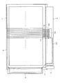
上記液晶表示装置は、図1に示すように、表示パネル1と駆動回路側基板であるゲートGS基板3およびソースGS基板5とによって液晶パネルが形成されている。また、上記液晶パネルはFPC7によって外部回路基板と接続されており、該液晶パネルへの駆動信号は該FPC7を介して外部回路より与えられる。
【0043】
上記表示パネル1は、図2に示すように、ガラス基板11a上に各種配線および画素等からなる配線層11bの形成された表示パネル側基板であるTFT基板11と、ガラス基板上に顔料分散型のアクリル系樹脂からなるカラーフィルタおよびITO(Indium Tin Oxide)のような透明導電膜からなる対向電極を形成したカラーフィルタ基板12とをシール剤13によって貼り合わせた後、両ガラス基板間に、表示に拘わる状態が電圧に応じて変化する表示媒体層としての液晶14を注入することによって形成される。
【0044】
また、上記表示パネル1におけるTFT基板11では、例えば、横300mm×縦222mmのサイズで、0.7mm厚のアルミノホウケイ酸ガラス基板が用いられる。そして、上記ガラス基板上に、Al(アルミ)薄膜からなる各種配線、画素電極、およびスイッチング素子となるTFT(Thin Film Transistor)が形成される。
【0045】
上記表示パネル1に形成される配線としては、複数のソースバスライン(ソース配線)、複数のゲートバスライン(ゲート配線)、さらに、画素電極の形成領域の周縁部に、ゲートバスラインと同層かつ同一の工程で形成されるパネル予備配線、端子部側の予備配線、非端子部側の予備配線、パネル内配線が形成される。但し、これらの予備配線は必ずしもゲートバスラインと同層に形成されるとは限らず、別層に形成されるものであってもよい。これらの配線構造については後述する。
【0046】
また、TFTは、ソースバスラインとゲートバスラインとの交差部の近傍に設けられ、例えばアモルファスシリコンを半導体層に用いて形成される。画素電極は、ITOのような透明導電膜から形成され、上記TFTを介してソースバスラインおよびゲートバスラインと接続される。
【0047】
次に、上記液晶表示装置に用いられるゲートGS基板3およびソースGS基板5について、ソースGS基板5を例にとって説明する。
【0048】
ソースGS基板5は、図2に示すように、例えば、ガラス基板51として縦4.5mm×横260mmのサイズの0.5mm厚のアルミノホウケイ酸ガラスを用い、該ガラス基板51上に、表示パネルのソースバスラインを駆動するための駆動回路52、駆動回路に接続されるソース出力配線、引き回し配線、予備配線等の各種配線からなる配線層53が形成されている。配線材料としては、例えばアルミが用いられが、上記各種配線の構成については後述する。上記駆動回路は、例えば、多結晶シリコンを半導体層として用いたTFTによって構成できる。また、ゲートGS基板3についても、ソースGS基板5とほぼ同様の構成である。
【0049】
以上の構造のソースGS基板5およびゲートGS基板3を、表示パネル1におけるTFT基板11のソース端子部領域およびゲート端子部領域において、ACF(Anisotropic Conductive Film)4を介して電気的に接続する。ここで、上記接続はACP(Anisotropic Conductive Paste)等を使用してもよく、接続される配線(または端子)同士の直接の接触が得られるのであれば、NCP(Non Conductive Resin Paste)を使用してもよい。
【0050】
次に、上記TFT基板11およびソースGS基板5における配線構造と、その接続関係とについて図3に基づいて説明する。尚、ゲートGS基板3における配線構造と、TFT基板11およびゲートGS基板3における配線の接続関係とについては、ソースGS基板5とほぼ同様であるため詳細な説明については省略する。
【0051】
上記TFT基板11において形成される各種配線としては、ゲートバスライン15、ソースバスライン16、パネル側予備配線17、非端子側予備配線18、端子側予備配線19、パネル内配線20がある。ゲートバスライン15およびソースバスライン16は、画素電極およびTFTとともに表示領域21を構成するが、表示領域21内における配線は図3において図示を省略している。
【0052】
パネル側予備配線17は、TFT基板11とソースGS基板5との接続部(基板接続部)よりTFT基板側(すなわち、パネル側)でソースバスライン16と交差して設けられている。パネル側予備配線17とソースバスライン16との間には窒化シリコン膜等からなる絶縁膜が設けられており、パネル側予備配線17とソースバスライン16とは電気的に接続されていない。また、パネル側予備配線17は、ソースバスライン16と交差しない部分でソースGS基板5との接続領域まで延設されている。
【0053】
非端子側予備配線18は、TFT基板11におけるソースGS基板5の接続されている側と反対側に設けられており、表示領域を通じて横切るように配設されたソースバスライン17と交差して設けられている。この非端子側予備配線18とソースバスライン17との交差部分が接続配線延在部となる。非端子側予備配線18とソースバスライン16との間には窒化シリコン膜等からなる絶縁膜が設けられており、非端子側予備配線18とソースバスライン16とは電気的に接続されていない。また、非端子側予備配線18は、ソースバスライン16と交差しない部分でゲートGS基板3との接続領域まで延設されている。
【0054】
端子側予備配線19は、ゲートGS基板3に形成されている後述するゲート基板内予備配線とソースGS基板5に形成されている後述するソース基板内予備配線54とを接続するための配線として形成されている。
【0055】
パネル内配線20は、ゲートGS基板3上のゲートドライバ32およびソースGS基板5上のソースドライバ55への駆動信号および電源電圧(すなわち、駆動電圧)を供給するための配線を、FPC7とゲートGS基板3およびソースGS基板5との間で接続するためにTFT基板11内に形成されている配線である。
【0056】
一方、上記ソースGS基板5において形成される各種配線としては、ソース基板内予備配線54、ソース入力配線56、ソース出力配線57、ドライバ側予備配線58がある。
【0057】
ソース入力配線56は、FPC7から入力される駆動信号および駆動電圧をソースドライバ55へ入力するための配線であり、このため、TFT基板11におけるパネル内配線20を介しての信号入力配線71と接続されている。上記FPC7では、例えば、ポリイミド基材上に銅(Cu)箔が複数の配線にパターニングされることにより信号入力配線71が形成される。
【0058】
ソース出力配線57は、ソースドライバ55で生成されたソース信号をTFT基板11上のソースバスライン16に出力するための配線であり、ソース出力配線57とソースバスライン16とが基板接続部において1対1に接続される。
【0059】
ドライバ側予備配線58は、TFT基板11とソースGS基板5との接続部(基板接続部)よりGS基板側(すなわち、ドライバ側)でソース出力配線57と交差して設けられている。ドライバ側予備配線58とソース出力配線57との間には窒化シリコン膜等からなる絶縁膜が設けられており、ドライバ側予備配線58とソース出力配線57とは電気的に接続されていない。また、ドライバ側予備配線58は、ソース出力配線57と交差しない部分でTFT基板11との接続領域まで延設されている。
【0060】
ソース基板内予備配線54は、ソースGS基板5におけるドライバ側予備配線58とTFT基板11における非端子側予備配線18とを電気的に接続するための接続配線の一部となる配線である。すなわち、ドライバ側予備配線58と非端子側予備配線18とは、ソース基板内予備配線54、端子側予備配線19、およびゲート基板内予備配線31を介して電気的に接続されている。
【0061】
このように、上記液晶表示装置では、パネル側予備配線17、ドライバ側予備配線58、ソース基板内予備配線54、端子側予備配線19、ゲート基板内予備配線31、および非端子側予備配線18が接続されることによって、図1に示す予備配線8が構成される。尚、上記予備配線8においては、パネル側予備配線17およびドライバ側予備配線58によって基板接続部修正用予備配線が構成され、ドライバ側予備配線58、ソース基板内予備配線54、端子側予備配線19、ゲート基板内予備配線31、および非端子側予備配線18によって接続配線修正用予備配線が構成される。
【0062】
また、図1の構成では予備配線8の本数は2本であり。図3の構成では3本であるが、本発明において上記予備配線8の配線本数は必要な修正可能数により決定されるものであり、特に限定されるものではない(1本のみでもよいし複数配線してもよい)。
【0063】
尚、上記予備配線8を複数本配設する場合、異なる予備配線同士は電気的に接続されない。このため、異なる予備配線同士が交差する箇所では、間に絶縁膜を設けて多層構造にて予備配線が配設される。その結果、予備配線の一部が最上層よりも下層に形成されることがある。しかしながら、上記予備配線を基板接続部において他の基板に形成されている予備配線と接続するためには、少なくとも基板接続部においては上記予備配線が最上層に形成されている必要がある。このような場合、少なくとも基板接続部においては全ての予備配線が最上層に位置するように形成し、これと接続されるべき同一の予備配線がより下層に形成される場合は、その交差箇所においてコンタクトホールを設けて異なる層に形成された予備配線同士を電気的に接続することができる。もちろんこれ以外に、設計の都合上、同一の予備配線を異なる層に形成する場合には、コンタクトホールによる接続が利用される。
【0064】
ここで、本実施の形態に係る液晶表示装置の製造方法についてその一例を説明する。
【0065】
表示パネル1を構成するTFT基板11については、まず0.7mm厚のガラス基板上にスパッタ法を用いてチタニウム膜、アルミニウム膜、窒化チタニウム膜を順次積層し、フォトリソグラフ・ドライエッチング技術を用いて、ゲートバスライン15、ゲート電極(図示せず)、ゲート側接続端子(図示せず)、パネル側予備配線17、端子側予備配線19、パネル内配線20およびソース側接続端子(図示せず)を形成する。
【0066】
次に、プラズマCVD法を用いて、ゲート絶縁膜となる窒化シリコン膜、半導体層となる真性アモルファスシリコン層、ソース電極コンタクト層およびドレイン電極コンタクト層となるn+アモルファスシリコン層を順次積層した後、フォトリソグラフ・ドライエッチング技術を用いて、窒化シリコン膜のゲート側接続端子及びソース側接続端子上となる部位にコンタクトホール(図示せず)を形成するとともに、n+アモルファスシリコン層と真性アモルファスシリコン層を島状にパターニングする。
【0067】
次に、スパッタ法を用いて、透明導電膜であるITO膜、タンタル膜、窒化タンタル膜を順次積層し、フォトリソグラフ・エッチング技術を用いて、ソースバスライン16、ソース電極(図示せず)およびドレイン電極(図示せず)を形成する。このとき、ソースバスライン16とソース側接続端子は、ゲート絶縁膜である窒化シリコン膜に設けられたコンタクトホールを介して電気的に接続される。
【0068】
また、ソース電極とドレイン電極とは、n+アモルファスシリコン層と真性アモルファスシリコン層からなる島状パターンの上で分離されるように形成されている。
【0069】
更に、n+アモルファスシリコン層と真性アモルファスシリコン層をエッチングすることによって、ソース電極コンタクト層(図示せず)、ドレイン電極コンタクト層(図示せず)およびチャネル領域(図示せず)を形成してTFTを構成する。
【0070】
次いでプラズマCVD法により保護層となる窒化シリコン膜を成膜し、そのドレイン電極上となる部位に、画素電極と電気的に接続する為のコンタクトホールをパターニングした後、スパッタ法により透明導電膜であるITO膜を成膜・パターニングして画素電極(図示せず)を形成する。
【0071】
そして、上記で得られた基板上にポリイミド系樹脂からなる配向膜を形成し、これをラビング法によって配向処理する。以上の工程を経て、表示パネル1を構成するTFT基板11を得ることができる。
【0072】
なお、以上の工程を経てTFT基板11が形成されるにあたり、ゲート側接続端子およびソース側接続端子は、外部と電気的に接続が可能となるように導電層が露出されることはいうまでもない。
【0073】
次に、表示パネル1を構成するカラーフィルタ基板12については、まず0.7mm厚のガラス基板上にアクリル系樹脂を基材とする顔料分散型のカラーフィルタを形成し、その上に、スパッタ法により、対向電極として透明導電膜であるITO膜を形成する。更に、ポリイミド系樹脂からなる配向膜を形成し、これをラビング法によって配向処理する。以上の工程をもって、表示パネル1を構成するカラーフィルタ基板12を得ることができる。
【0074】
次に、カラーフィルタ基板12上にスクリーン印刷法を用いてシール剤を塗布し、TFT基板11上に乾式散布法を用いてスペーサ材を散布する。そしてカラーフィルタ基板12とマトリクス基板11とを互いの配向膜の形成面が一定の間隙をもって対向するようにして貼り合わせる。更に、カラーフィルタ基板12とTFT基板11との間に、液晶を注入することによって、表示パネル1が形成される。
【0075】
次に、ソースGS基板5の形成方法について説明する(ゲートGS基板3も同様の方法で形成される)。
【0076】
表示パネル1におけるTFT基板11と同様の製法を用いて、アルミノホウケイ酸からなるガラス基板上に、ポリシリコンからなる薄膜トランジスタを使ったソースドライバ55、該ソースドライバ55と接続されるソース出力配線57、接続端子を形成する。
【0077】
次に、表示パネル1におけるTFT基板11とソースGS基板5との接続方法について説明する(TFT基板11とゲートGS基板3も同様の方法で接続される)。
【0078】
これは、ソースGS基板5におけるソースドライバ55の形成面側が、TFT基板11のソース側端子部領域に対向するように、ソースGS基板5とTFT基板11との接続端子同士をACFを介して重畳させた後、300℃に加熱されたツールを重畳した箇所に押し当てることによって行なわれる。このとき、ツールは、合金工具鋼鋼材からなる。
【0079】
次に、TFT基板11とFPC7との接続方法について説明する。
【0080】
FPC7の接続端子とTFT基板11の接続端子とを、ACFを介して対向するように重畳させた後、重畳した個所に300℃に加熱されたツールを押し当てることによって、接続される。
【0081】
以上のようにして、本実施の形態に係る液晶表示装置が形成される。
【0082】
上記液晶表示装置において、電源電圧の劣化を防止するため、ソースバスライン16が互いに隣接する複数本ずつのグループに区分けされ、各グループ毎のソースバスライン16に対して異なるソースドライバ55により駆動する分割駆動が一般に行われている。このような場合、上記予備配線8におけるパネル側予備配線17およびドライバ側予備配線58は、各ソースドライバ55毎に設けられる。しかしながら、ソース基板内予備配線54、端子側予備配線19、ゲート基板内予備配線31、および非端子側予備配線18は、各ソースドライバ55毎に別個に設けても良いし、あるいは複数のソースドライバ55毎に共通して設けても良い(尚、全てのソースドライバ55で共通とは限らない)。ソース基板内予備配線54、端子側予備配線19、ゲート基板内予備配線31、および非端子側予備配線18を、各ソースドライバ55毎に別個に設ける構成を図4(a)に示し、複数のソースドライバ55毎に共通して設ける構成を図4(b)に示す。
【0083】
尚、上記説明では、ソース側においての予備配線構成を示したが、ゲート側においても同様の設計にて予備配線を設けることが可能である。
【0084】
上記構成の液晶表示装置における各配線のピッチおよび配線幅の具体的な構成例は以下の通りである。但し、以下の各寸法は、配線全体にかかるものとは限らず、少なくとも基板接続部の接続端子における寸法を示すものである。
・FPC7−TFT基板11接続部:
配線ピッチ0.3mm;信号入力配線71の幅(FPC端子幅)0.1mm;パネル内配線20の幅(TFTパネル端子幅)0.2mm
・TFT基板11−ゲートGS基板3またはソースGS基板5接続部(駆動回路駆動用の信号・電源伝送配線/予備配線(伝送部分)):
配線ピッチ0.3mm;非端子側予備配線18および端子側予備配線19の幅(TFTパネル端子幅)0.2mm;ゲート基板内予備配線31,ソース基板内予備配線54,ゲート入力配線およびソース入力配線56の幅(GS基板端子幅)0.1mm
・TFT基板11−ゲートGS基板3またはソースGS基板5接続部(パネル絵素部への出力信号接続部):
配線ピッチ0.07mm;ソースバスライン16の幅(TFTパネル端子幅)0.04mm;ソース出力配線57(GS基板端子幅)0.04mm(ソース側)
配線ピッチ0.1mm;パネル側予備配線17の幅(TFTパネル端子幅)0.07mm;ドライバ側予備配線58(GS基板端子幅)0.04mm(ソース側予備配線)
配線ピッチ0.2mm;ゲートバスライン15の幅(TFTパネル端子幅)0.1mm;ゲート出力配線(GS基板端子幅)0.1mm(ゲート側)
上記構成の液晶表示装置においては、表示パネル側基板であるTFT基板11と駆動回路側基板であるソースGS基板5(またはゲートGS基板3)との接続部に発生した接続不良を修正する予備配線を搭載することにより、従来は駆動回路基板を取り替えることにより修正を行っていた修理作業をレーザー修正で行うことができる。このため、修理にかかる工程数を大幅に低減でき、人件費の低減およびスループットの向上を図ることができる。
【0085】
また、接続不良の生じた駆動回路側基板を廃棄する必要が無く、材料費が低減できる。
【0086】
さらに、修理で発生する2次不良の発生を抑制することができる。同時に、2次不良が発生しにくいため信頼性の高いモジュールを提供できる。
【0087】
また、回路基板の交換修理で発生する、表示パネルの破壊(接続端子の断線など)を防止できる。
【0088】
次に、上記構造の予備配線を備えた液晶表示装置において、基板接続部にて接続不良が生じた場合の修正方法を説明する。
【0089】
図5(a)は、基板接続部に導電性の異物9aが混入することにより発生したリーク症状の第1の修正方法を示す。尚、図5(a)では、ソース信号XおよびYを出力する隣接した2本のソースバスラインが異物9aによってリークした状態を示している。
【0090】
導電性の異物9aには通常数10μmの厚みがあり、ガラス基板を通してレーザー等で分断することは困難であり、予備配線による修正が必要となる。このため、信号XおよびYを出力する信号線、すなわち、ソースバスライン16およびソース出力配線57は、パネル側予備配線17およびソース出力配線57の内側にて合計4箇所がレーザーにより分断され(図中、×印で示す)、電気的に絶縁される。ここで、ソースバスライン16およびソース出力配線57の膜厚は約3000Åであり、これらの配線はエキシマレーザーによる分断が可能である。
【0091】
次に、信号XおよびYを出力するソースバスライン16とパネル側予備配線17とのクロス部分、およびソース出力配線57とドライバ側予備配線58とのクロス部分(交差部分)をレーザーにより合計4箇所短絡する(図中、黒丸で示す)。
【0092】
以上の作業により、信号XおよびYは各々固有の信号を、上記リーク部分を迂回し、予備配線を介して表示パネル部へと出力することができる(図中、信号XおよびYの流れを太線で示す)。
【0093】
また、図5(b)は、図5(a)の場合と同様に接続部に導電性9aの異物が混入することにより発生したリーク症状の第2の修正方法を示す。
【0094】
図5(b)の構成では、異物9aにより信号XおよびYを出力する信号線がリーク症状となっているのは図5(a)の場合と同じであるが、上記リーク箇所を迂回するための信号線の分断、および信号線と予備配線との短絡箇所が信号Xに対応した部分のみとなっている。この結果、信号Xは予備配線を迂回した信号の流れとなるが、信号Yは予備配線を迂回しないで、ソースドライバ55からソース出力配線57およびソースバスライン16を介して表示パネルへと信号が流れている。この修正方法によっても、図5(a)に示した方法と同様の効果を得ることができる。
【0095】
次に、図5(c)は、基板接続部に浮き9bが生じオープン状態(絶縁性の異物や気泡によって、ACFによる接続端子間の電気的な接続が得られない接続不良)となった症状の修正方法を示す。
【0096】
この場合は、信号XおよびYを出力する信号線と予備配線とのクロス部分をレーザーにより合計4箇所短絡する。この結果、ソースドライバ55から出力された信号XおよびYは、上記オープン部分を迂回し、予備配線を介して表示パネル部へと伝達される(図中、信号XおよびYの流れを太線で示す)。
【0097】
以上の修正方法は、リーク症状およびオープン症状のそれぞれの場合の修正方法を示したものであるが、リーク症状およびオープン症状が組み合わされた接続不良の場合でも、上記の方法を組み合わせることにより修正が可能である。この時、不良発生の傾向を把握し、予備配線本数を設計段階で調整することが重要である。
【0098】
上記図5の説明では、基板接続部における接続不良を予備配線にて修正する場合を示したが、本実施の形態に係る液晶表示装置は、ソースバスライン(もしくはゲートバスライン)の断線不良が生じた場合にも予備配線を用いた修正が可能である。
【0099】
図6にソース断線が生じた液晶表示装置の例を示す。図6の例では、図中、■印で示す箇所にソースバスライン16の断線が生じているものとする。このとき、特に修正を行わなければ、ソースバスライン55から出力される信号は、上記断線の生じているソースバスライン16で断線箇所より先の信号供給が途切れることとなる。
【0100】
この場合の修正方法としては、断線の生じているソースバスライン16において、該ソースバスライン16に繋がるソース出力配線57とドライバ側予備配線58とのクロス部分(交差部分)をレーザーにより短絡し、さらに、表示エリアの外まで延びた該ソースバスライン16と非端子側予備配線18とのクロス部分(交差部分)をレーザーにより短絡する。ここで、上記短絡箇所を含むドライバ側予備配線58と非端子側予備配線18とは同一の予備配線8に属するものである。
【0101】
これにより、断線の生じているソースバスライン16において、断線箇所より端子側(すなわち、ソースGS基板5と接続されている側)では、ソース出力配線57およびソースバスライン16を介して信号が供給される一方、非端子側(すなわち、ソースGS基板5と接続されていない側)では、ドライバ側予備配線58、ソース基板内予備配線54、端子側予備配線19、ゲート基板内予備配線31、および非端子側予備配線18を介して信号が供給される。
【0102】
また、上記図6の構成においては、ソースGS基板5上のドライバ側予備配線58とTFT基板11の非端子側予備配線18との接続が、ゲートGS基板3およびソースGS基板5上の予備配線を介して行なわれる。このため、ソースバスライン16の断線修正時において、予備配線8を介して非端子側から供給される信号は、ソースバスライン16とパネル側予備配線17との絶縁膜を介した交差部を通過しないため、寄生容量の発生を抑え、ソース信号電圧のなまりを防止することができる。さらに、このことは、ゲートバスラインの冗長についても同様の構造を持てば、同様の効果を得ることができる。
【0103】
また、本実施の形態においては、パネル側予備配線17とドライバ側予備配線58とは、ソースバスライン16またはゲートバスライン15よりも線幅が太く形成されることが好ましい。これにより、冗長配線を伝搬する信号電圧に対する抵抗をバスラインの抵抗と同程度に抑制することができる。
【0104】
予備配線の配線幅、および、接続端子部の幅を広く設定することにより、修正ラインのバスライン抵抗と修正のない場所のバスライン抵抗とをほぼ均一にすることができる。これにより、バスライン間の配線抵抗のばらつきにより発生する表示ムラを抑制することができ、表示品位の向上を図ることができる。
【0105】
尚、上記説明における構成はあくまで一例であり、本発明はこれに限定されるものではなく、種々の変形例を取ることが可能である。例えば、基板接続部における予備配線の変形例を図7に示す。
【0106】
図7に示す構成では、パネル側予備配線17およびドライバ側予備配線58は、同一のソースドライバ55にて駆動される複数のソースバスライン16の両側を迂回するように配置されている。これにより、上記予備配線(すなわち、パネル側予備配線17およびドライバ側予備配線58)がソースバスライン16とソース出力配線57との接続領域を囲むようにして配置される。なお、図7では、上記予備配線が2本の場合の構成を示しているが、この本数は特に限定されない。
【0107】
ここで、上記図7の構成における基板接続部での修正方法を説明する。先ず、基板接続部においてオープン不良が発生した場合の修正方法を図7(a)に示す。例えば、オープン不良箇所9cの発生している信号線(ここでは、4本)について、うち左から2本目と3本目との間において、パネル側予備配線17およびドライバ側予備配線58をレーザーにより分断する(図中、×印で示す)。これにより、接続領域を囲むようにして配置された2本の予備配線が4本の独立した予備配線として使用できる。
【0108】
さらに、修正される4本の信号線のうち、ソースバスライン16とパネル側予備配線17との交差部分をレーザーによって短絡し、ソース出力配線57とドライバ側予備配線58との交差部分をレーザーによって短絡する。この時の短絡箇所は、図中黒丸で示されるようになり、修正される4本の信号線について外側の2本は外側の予備配線によって接続され、内側の2本は内側の予備配線によって接続される。この方法によれば、(予備配線本数×2)本の信号線についてまで、オープン症状の修正が可能である。
【0109】
次に、基板接続部においてリーク不良が発生した場合の修正方法を図7(b)に示す。例えば、リーク不良箇所9dの発生している信号線(ここでは、5本)について、うち左から2本目と3本目との間において、パネル側予備配線17およびドライバ側予備配線58をレーザーにより分断する(図中、×印で示す)。これにより、接続領域を囲むようにして配置された2本の予備配線が4本の独立した予備配線として使用できる。また、リーク不良箇所9dの発生している5本の信号線うち、左から1〜4本目の信号線について、予備配線の内側でリーク不良箇所9dと分断される(図中、×印で示す)。
【0110】
さらに、修正される5本の信号線のうち、左から1〜4本目の信号線について、ソースバスライン16とパネル側予備配線17との交差部分をレーザーによって短絡し、ソース出力配線57とドライバ側予備配線58との交差部分をレーザーによって短絡する。この時の短絡箇所は、図中黒丸で示されるようになり、修正される4本の信号線について外側の2本は外側の予備配線によって接続され、内側の2本は内側の予備配線によって接続される。また、リーク不良箇所9dの発生している5本の信号線のうち、最も右側の信号線は他の4本の信号線の分断によって独立する。この方法によれば、(予備配線本数×2+1)本の信号線についてまで、リーク症状の修正が可能である。
【0111】
また、上記図7の構成において、不良発生箇所が予備配線による修正可能数よりも少ない場合には、修正に用いられる予備配線と交差する信号線の本数が少なくなるようにすることで、予備配線に生ずる寄生容量を低減できる。
【0112】
また、ドライバ側予備配線58とソース基板内予備配線54との接続構成における変形例を図8ないし図10に示す。
【0113】
図1に示す構成では、パネル側予備配線17、ドライバ側予備配線58、およびソース基板内予備配線54がS字形状(パネル側予備配線17とドライバ側予備配線58の接続箇所と、ドライバ側予備配線58とソース基板内予備配線54の接続箇所が、ソースバスライン16およびソース出力配線57の配設領域を挟み、両側に別れて配置されている)に配置されているが、図8に示す構成では、パネル側予備配線17、ドライバ側予備配線58、およびソース基板内予備配線54がF字形状(パネル側予備配線17とドライバ側予備配線58の接続箇所と、ドライバ側予備配線58とソース基板内予備配線54の接続箇所がソースバスライン16およびソース出力配線57の配設領域の片側に共に配置されている)に配置されている。
【0114】
また、図9に示す構成では、パネル側予備配線17、ドライバ側予備配線58、およびソース基板内予備配線54が8字形状(パネル側予備配線17とドライバ側予備配線58の接続箇所と、ドライバ側予備配線58とソース基板内予備配線54の接続箇所が、ソースバスライン16およびソース出力配線57の配設領域を挟み、両側にそれぞれ配置されている)に形成されている。この構成によれば、ソースバスライン16の断線が生じた場合の修正において、断線が生じたソースバスラインの位置に応じて、修正に用いられるドライバ側予備配線58と交差するソース出力配線57の本数が少なくなるようにすることで、ドライバ側予備配線58に生ずる寄生容量を低減できる。
【0115】
更に上記によれば、パネル側予備配線17とドライバ側予備配線58がソースバスライン16およびソース出力配線57の配設領域を挟み、両側で接続されているので、仮に一方のパネル側予備配線17とドライバ側予備配線58との接続においてオープン症状が発生したとしても、もう一方のパネル側予備配線17とドライバ側予備配線58との接続を利用して修正を行うことができる。
【0116】
また、図10に示す構成では、2つのソースドライバ55のブロックをひとかたまりとして、予備配線を配置している。すなわち、パネル側予備配線17およびドライバ側予備配線58が、2つ分のソースドライバ55によって駆動される複数のソースバスライン16およびソース出力配線57にわたって配置され、ソース基板内予備配線54は、上記ドライバ側予備配線58の中央部(2つのソースドライバ55の間)で該ドライバ側予備配線58と接続される。さらに、図10の構成では、非端子側予備配線18へのソース信号の取り出しは、2つのブロックで2本となっている。
【0117】
また、ドライバ側予備配線58と非端子側予備配線18との接続については、上記説明では、ゲートGS基板3およびソースGS基板5を介した予備配線によって接続がなされている。しかしながら、ドライバ側予備配線58と非端子側予備配線18との接続は、TFT基板11内のみで行うことも可能である。この場合は、非端子側予備配線18は、パネル側予備配線17と接続される構成とすればよい。
【0118】
しかしながら、ドライバ側予備配線58と非端子側予備配線18とをTFT基板11内のみで接続する構成では、ソースバスライン16との交差箇所が多くなり、予備配線に発生する寄生容量が増大するため、ドライバ側予備配線58と非端子側予備配線18との接続をゲートGS基板3およびソースGS基板5を介した予備配線によって接続する構成が好ましい。また、上記説明では、ドライバ側予備配線58と非端子側予備配線18との接続は、ゲートGS基板3およびソースGS基板5の2つの駆動回路側基板を介して接続されているが、1つの駆動回路側基板(ドライバ側予備配線58と非端子側予備配線18との接続についてはソースGS基板5)を介して接続されるものであってもよい。
【0119】
尚、本実施の形態においては、本発明を液晶表示装置に適用する場合について、説明したが、これに限定されるものではなく、プラズマ表示装置、有機EL表示装置等、端子部を持つ表示装置であれば本発明の適用が可能である。
【0120】
また本発明では、液晶表示装置のようなアクティブマトリクス型における表示パネル側基板と駆動回路側基板との接続についての使用に限定されるものではない。すなわち、複数の配線を有する回路基板同士の接続において、その基板接続部にて配線同士も接続されるような構成であれば、その基板接続部の構造において本発明を適用することが可能であり、これらの回路基板の使用目的は特に限定されない。
【0121】
【発明の効果】
本発明の配線基板の接続構造は、以上のように、基板接続部にて接続される各基板に設けられた複数の接続配線同士が電気的に接続されるように、2枚の配線基板同士を接続する際の配線基板の接続構造において、上記各配線基板は、それぞれの配線基板に形成された接続配線に対して絶縁膜を介して該接続配線と交差するように設けられた少なくとも1本の予備配線を有しており、上記基板接続部では、上記接続配線と共に、各配線基板に形成された予備配線同士も接続されている構成である。
【0122】
それゆえ、上記配線基板の接続部において異物のかみ込みなどによる接続配線間の接続不良が発生した場合、基板の剥離、清掃、再接続といった、従来の修正方法における煩雑な工程が必要なく、レーザー照射のみによる容易な修正が可能となるといった効果を奏する。また、基板の剥離時における2次不良を抑制できるといった効果を併せて奏する。
【0123】
本発明の表示装置は、以上のように、表示パネル側基板と駆動回路側基板との基板接続部にて接続される各基板に設けられた複数の接続配線同士が電気的に接続されるように、表示パネル側基板と駆動回路側基板とが接続される表示装置において、上記表示パネル側基板および駆動回路側基板は、それぞれの基板に形成された接続配線に対して絶縁膜を介して該接続配線と交差するように設けられた少なくとも1本の予備配線を有しており、上記基板接続部では、上記接続配線と共に、上記表示パネル側基板および駆動回路側基板のそれぞれに形成された予備配線同士が接続されて、基板接続部修正用予備配線を構成している。
【0124】
それゆえ、例えば液晶表示装置等のアクティブマトリクス型の表示装置において、表示パネルと駆動回路(ゲートドライバやソースドライバ等)を異なる基板上に作成し、これらの基板を接続して表示装置を構成する場合に、表示パネル側基板と駆動回路側基板との接続に上述の配線基板の接続構造を使用することで、接続不良の発生した基板の接続において、レーザー照射のみによる容易な修正が可能となるといった効果を奏する。また、基板の剥離時における2次不良を抑制できるといった効果を併せて奏する。
【0125】
また、上記表示装置は、さらに、上記表示パネル側基板における接続配線の断線を修正するための接続配線修正用予備配線を有し、上記接続配線修正用予備配線が上記基板接続部修正用予備配線に接続されている構成とすることができる。
【0126】
それゆえ、上記接続配線修正用予備配線を設けることによって、基板接続部における接続不良の修正に加えて、表示パネル側基板における接続配線の断線(ゲートバスラインやソースバスラインの断線)をも修正できる。このとき、駆動回路から接続配線修正用予備配線および基板接続部修正用予備配線に信号を出力するための出力端子を低減でき、基板の小型化が図れるといった効果を奏する。
【0127】
また、上記表示装置では、上記接続配線修正用予備配線は、上記基板接続部修正用予備配線を形成する駆動回路側基板の予備配線から少なくとも1つの駆動回路側基板の接続配線と交差しない領域を経由して設けられている構成とすることが好ましい。
【0128】
それゆえ、上記接続配線修正用予備配線と接続配線との交差箇所を減らすことができ、接続配線修正用予備配線に発生する寄生容量を低減することができるといった効果を奏する。
【0129】
また、上記表示装置では、上記基板接続部修正用予備配線は、上記表示パネル側基板および駆動回路側基板のそれぞれに形成された予備配線同士が、これらの予備配線と交差する接続配線の配置方向の両側を経由して、表示パネル側基板および駆動回路側基板の間で接続される構成とすることができる。
【0130】
それゆえ、上記基板接続部修正用予備配線が、接続配線の配置方向の両側を経由しているため、接続配線との交差箇所の間で該基板接続部修正用予備配線を分断することによって、1本の基板接続部修正用予備配線によって、2本の接続配線に対して冗長配線を与えることができる。これにより、基板接続部修正用予備配線の配置領域の増大を最小限として、修正不良可能数を増やすことができるといった効果を奏する。
【0131】
また、上記表示装置では、上記基板接続部修正用予備配線は、上記表示パネル側基板および駆動回路側基板のそれぞれに形成された予備配線の配線幅が、これらの予備配線と交差する接続配線の線幅よりも太くなるように設定されている構成とすることが好ましい。
【0132】
それゆえ、上記基板接続部修正用予備配線の線幅を太くすることで、基板接続部修正用予備配線を伝搬する信号電圧に対する抵抗を、接続配線の抵抗と同程度に抑制することができる。これにより、接続配線間の配線抵抗のばらつきにより発生する表示ムラを抑制することができ、表示品位の向上を図ることができるといった効果を奏する。
【図面の簡単な説明】
【図1】本発明の一実施形態を示すものであり、液晶表示装置の全体構成を示す平面図である。
【図2】図1のA−A断面を示すものであり、上記液晶表示装置の接続部の構成を示す断面図である。
【図3】上記液晶表示装置の詳細な配線構造を示す平面図である。
【図4】上記液晶表示装置におけるドライバ側予備配線とソース基板内予備配線との接続例を示す図であり、図4(a)はソース基板内予備配線を共有しない場合の平面図、図4(b)はソース基板内予備配線を共有する場合の平面図である。
【図5】上記液晶表示装置における基板接続部の接続不良の修正例を示すものであり、図5(a)はリーク症状の修正における第1の例を示す平面図、図5(b)はリーク症状の修正における第2の例を示す平面図、図5(c)はオープン症状の修正における例を示す平面図である。
【図6】上記液晶表示装置におけるソースバスラインの断線の修正例を示す平面図である。
【図7】上記液晶表示装置における基板接続部の接続不良の修正例を示すものであり、図7(a)はオープン症状の修正における例を示す平面図、図7(b)はリーク症状の修正における例を示す平面図である。
【図8】上記液晶表示装置におけるドライバ側予備配線とソース基板内予備配線との図1とは異なる接続例を示す平面図である。
【図9】上記液晶表示装置におけるパネル側予備配線とドライバ側予備配線との接続構成における変形例を示す平面図である。
【図10】上記液晶表示装置におけるパネル側予備配線とドライバ側予備配線との接続構成における変形例を示す平面図である。
【図11】従来のTCP方式による表示装置の概略平面図である。
【図12】従来のCOG方式による表示装置の概略平面図である。
【図13】従来のGOG方式による表示装置の概略平面図である。
【図14】TCP方式の基板接続における不良発生箇所の状態を示す図であり、図14(a)は図11のA−A’断面図、図14(b)は図14(a)のAY−AY’断面図である。
【図15】GOG方式の基板接続における不良発生箇所の状態を示す図であり、図15(a)は図13のB−B’断面図、図15(b)は図15(a)のBY−BY’断面図である。
【符号の説明】
1 表示パネル
3 ゲートGS基板
5 ソースGS基板(配線基板、駆動回路側基板)
11 TFT基板(配線基板、表示パネル側基板)
15 ゲートバスライン
16 ソースバスライン(接続配線)
17 パネル側予備配線(予備配線、基板接続部修正用予備配線)
18 非端子側予備配線(接続配線修正用予備配線)
19 端子側予備配線(接続配線修正用予備配線)
31 ゲート基板内予備配線(接続配線修正用予備配線)
54 ソース基板内予備配線(接続配線修正用予備配線)
55 ソースドライバ(駆動回路)
57 ソース出力配線(接続配線)
58 ドライバ側予備配線(予備配線、基板接続部修正用予備配線、接続配線修正用予備配線)[0001]
BACKGROUND OF THE INVENTION
The present invention relates to a wiring board connection structure used when a drive circuit board is mounted on a display panel in an active matrix display device such as a liquid crystal display device, an organic EL display device, and an inorganic EL display device.
[0002]
[Prior art]
Currently, the connection between the display panel in the active matrix display device such as a liquid crystal display device and the drive circuit that drives the display panel uses a TCP (Tape Carrier Package) method, a COG (Chip on Glass) method, and low-temperature polycrystalline silicon technology. A monolithic method or the like is used.
[0003]
As shown in FIG. 11, in the TCP method, a
[0004]
In the COG method, as shown in FIG. 12, a plurality of
[0005]
The TCP method and the COG method have a long track record of mass production and are advantageous in terms of product quality and reliability. However, there are problems such as a large number of parts and high material costs and mounting processing costs.
[0006]
The monolithic method is a method in which the gate IC and the source IC in the COG method are formed in a display panel by applying a low-temperature polycrystal technology. Since this method can reduce the number of parts as compared with the TCP method and the COG method, the material cost and the mounting processing cost can be reduced. However, the design on the display panel side becomes complicated, and the cost for this increases. Moreover, it is disadvantageous for increasing the size of the display panel, and the range of use is limited.
[0007]
The GOG (Glass on Glass) method using the same amorphous silicon as the TCP method or the COG method for the display panel, which is equivalent to or less than the monolithic method in terms of material cost, is used, for example, in the above three methods. 283727. In the GOG method, as shown in FIG. 13, a signal input from the FPC 124 passes through a wiring on the
[0008]
In the GOG method, a drive circuit portion that causes a reduction in the yield rate in the monolithic method can be created as a gate GS122 and a source GS123 in separate processes, so that an increase in cost of the
[0009]
[Problems to be solved by the invention]
However, in the above-described conventional configuration, particularly in the TCP method and the GOG method, a substrate on which a display panel is formed (hereinafter referred to as a display panel side substrate) and a substrate on which an IC serving as a drive circuit is formed (hereinafter referred to as driving). In some cases, an open symptom or a leak symptom may occur due to a connection abnormality such as a foreign object biting in a connection portion with a circuit-side board). And in the correction method in such a case, the following problems arise.
[0010]
In the correction method of the connection abnormality location in the TCP method, the TCP at the location where the connection failure between the display panel side substrate and the drive circuit side substrate has occurred is once peeled off, and the residue of the connection resin remaining on the panel surface is cleaned. The operation of connecting a new TCP or IC is performed again. However, such a correction method has a problem that there are many steps related to the correction work and the work efficiency is low.
[0011]
In addition, for the open symptom and leakage symptom due to abnormal connection between substrates such as foreign object biting in the GOG method, when the same correction method as the TCP method is applied, there are the following problems in addition to the work efficiency problem Arise. In other words, although the GOG method is advantageous in comparison with other methods in terms of cost, the increase in the defect occurrence rate due to the inclusion of foreign objects in the GOG connection and the difficulty in replacing the GS when a connection defect occurs are major problems. It becomes.
[0012]
First, an increase in the defect occurrence rate due to the inclusion of foreign matter at the substrate connection location in the GOG method will be described with reference to FIGS. 14 (a) and 14 (b) and FIGS. 15 (a) and 15 (b). FIG. 14A is a cross-sectional view taken along the line AA ′ of FIG. 11 and shows a case where a foreign object is caught between connected substrates. FIG. 15A is a cross-sectional view taken along the line BB ′ of FIG. 13 and shows a case where foreign matter is caught between connected substrates.
[0013]
In the case of the TCP system, as shown in FIG. 14A, the
[0014]
On the other hand, in the case of the GOG method, as shown in FIG. 15A, the drive circuit side substrate is not flexible. Not only the
[0015]
In the case of the GOG method, the wiring on the GS glass serving as the base material of the drive circuit side substrate is formed of a thin film, and the thickness thereof is 1 μm or less. For this reason, the conductive particles (φ5 to 10 μm) in the anisotropic conductive film (ACF) serving as a connection material for both substrates aggregate not only in the terminal portion but also in the space between the terminals, and there is a leakage symptom due to the connection of the conductive particles. Likely to happen. On the other hand, in the TCP method, the thickness of the wiring on the TCP is about 10 to 30 μm, which is sufficiently larger than the thickness of the wiring formed by the thin film on the GS glass, and the aggregation of particles between the terminals hardly occurs.
[0016]
Next, it is difficult to replace the drive circuit when a wiring connection failure occurs at the connection portion between the substrates. However, when the GOG method is applied to a large model, the size of the drive circuit side substrate becomes large (15 When applied to a “class module, the length of the long side of the substrate is about 300 mm), and the driver circuit side substrate or the display panel side substrate is likely to break during peeling of the driver circuit side substrate.
[0017]
Further, even if there is only one connection failure portion, it is necessary to replace the entire substrate on the drive circuit side, and it is not an operation of replacing individual TCPs as in the TCP method.
[0018]
As a method for correcting the connection failure due to the inclusion of foreign matter, a method of dividing the foreign matter by laser irradiation is also conceivable, but the conductive foreign matter usually has a thickness of several tens of μm and passes through the glass substrate without damaging the electrode terminal. It is technically difficult to divide only foreign matter.
[0019]
As described above, especially in the GOG method, due to an increase in the connection failure occurrence rate and difficulty in correction work, display panel destruction due to correction errors, an increase in work man-hours, an increase in repair material costs, and secondary defects during correction Occurrence of problems, deterioration of quality, and the like become problems.
[0020]
The present invention has been made to solve the above-described problems, and an object of the present invention is to connect a wiring substrate to be connected at a connection portion between a display panel side substrate and a drive circuit side substrate in an active matrix display device. It is an object of the present invention to provide a wiring board connection structure that can easily correct a connection failure between wirings while suppressing the occurrence of a secondary failure.
[0021]
[Means for Solving the Problems]
In order to solve the above-described problem, the wiring board connection structure of the present invention includes two pieces so that a plurality of connection wirings provided on each board connected by the board connecting portion are electrically connected to each other. In the wiring board connection structure when connecting the wiring boards to each other, each of the wiring boards is provided so as to intersect the connection wiring via an insulating film with respect to the connection wiring formed on each wiring board. In addition, at least one spare wiring is provided, and in the board connecting portion, the spare wiring formed on each wiring board is connected together with the connection wiring.
[0022]
Alternatively, in order to solve the above problems, the wiring board connection structure of the present invention includes a plurality of connection wirings provided on one side of a pair of wiring boards and a plurality of connection wirings provided on the other side of the board connection part. In the connection structure of the wiring boards that are electrically connected to each other, each of the wiring boards has at least one spare wiring provided so as to intersect with the connection wiring via an insulating film. The board connecting portion is characterized in that the spare wiring of the one wiring board and the spare wiring of the other wiring board are electrically connected.
[0023]
According to the above configuration, if a connection failure occurs between connection wires due to foreign object biting or the like at the connection portion of the wiring board, it can be corrected by short-circuiting the connection wire in which the connection failure has occurred and the spare wire. It becomes. For example, when an open symptom of the connection wiring occurs in the board connection part, the connection wiring and the spare wiring are short-circuited by irradiating a laser to an intersection between the connection wiring in which the open symptom occurs and the spare wiring, and the spare wiring A signal or voltage can be supplied to the connection wiring through the terminal. If the connection failure is a symptom of leakage, cut the connection wiring near the leak location by laser irradiation, divide the leak location from the connection wiring, short-circuit the connection wiring and the spare wiring, and pass through the spare wiring. A signal or voltage can be supplied to the connection wiring.
[0024]
This eliminates the need for complicated steps in the conventional correction method such as peeling, cleaning, and reconnection of the substrate in connection of the substrate in which the connection failure occurs, and allows easy correction only by laser irradiation. In addition, secondary defects such as substrate cracking during substrate peeling can be suppressed.
[0025]
In the display device of the present invention, in order to solve the above-described problem, a plurality of connection wirings provided on each substrate connected at a substrate connection portion between the display panel side substrate and the drive circuit side substrate are electrically connected to each other. In the display device in which the display panel side substrate and the drive circuit side substrate are connected so as to be connected, the display panel side substrate and the drive circuit side substrate are insulating films with respect to connection wirings formed on the respective substrates. And at least one spare wiring provided so as to intersect the connection wiring via the connection wiring. In the substrate connection portion, each of the display panel side substrate and the drive circuit side substrate is provided together with the connection wiring. The formed spare wirings are connected to each other to constitute a board connecting portion correcting spare wiring.
[0026]
Alternatively, in order to solve the above problems, the display device of the present invention has a display panel side substrate having a display area and a drive circuit side substrate having a drive circuit, and is provided on the display panel side substrate. In the display device in which a plurality of connection wirings and a plurality of connection wirings provided on the drive circuit side substrate are electrically connected at a substrate connection part outside the display area, the display panel side substrate and the drive circuit side substrate Each has at least one spare wiring provided so as to intersect the connection wiring via an insulating film, and the substrate connection section includes the spare wiring on the display panel side substrate and the drive circuit. The auxiliary wiring of the side substrate is electrically connected to constitute the auxiliary wiring for correcting the board connecting portion.
[0027]
According to the above configuration, for example, in an active matrix display device such as a liquid crystal display device, a display panel and a driving circuit (gate driver, source driver, etc.) are formed on different substrates, and these substrates are connected to display. When the device is configured, the above-described wiring board connection structure can be used to connect the display panel side substrate and the drive circuit side substrate.
[0028]
This eliminates the need for complicated steps in the conventional correction method such as peeling, cleaning, and reconnection of the substrate in connection of the substrate in which the connection failure occurs, and allows easy correction only by laser irradiation. In addition, secondary defects such as substrate cracking during substrate peeling can be suppressed.
[0029]
Further, the display device includes a plurality of drive circuits provided in parallel on the drive circuit side substrate, and the plurality of connection wirings are divided into a plurality of groups adjacent to each other. Each can be configured to be electrically connected to a connection wiring and a spare wiring belonging to each of the above groups.
[0030]
The display device further includes a connection wiring correction spare wiring for correcting a disconnection of the connection wiring in the display panel side substrate, and the connection wiring correction spare wiring is the substrate connection portion correction spare wiring. The connection wiring of the display panel side substrate is extended to the connection wiring extending portion provided outside the display area. The connection wiring correction spare wiring is electrically connected to the connection wiring of the display panel side substrate at the connection wiring extending portion, and is also electrically connected to the substrate connection correction wiring. It can be configured.
[0031]
According to the above configuration, by providing the connection wiring correction spare wiring, in addition to correcting the connection failure in the substrate connection portion, disconnection of the connection wiring in the display panel side substrate (disconnection of the gate bus line or the source bus line) ) Can also be corrected.
[0032]
In the display device, the connection wiring correction spare wiring is connected to at least one drive circuit side substrate from the drive circuit side substrate preliminary wiring that forms the substrate connection portion correction spare wiring. Alternatively, it is preferable that the connection wiring correction spare wiring is provided from a spare wiring on the drive circuit side substrate via a region that does not intersect with at least one connection wiring on the drive circuit side substrate.
[0033]
The connection between the connection wiring correction spare wiring and the board connection portion correction spare wiring is connected only by the wiring in the display panel side substrate in addition to the connection via the drive circuit side substrate as described above. It can also be considered. However, in this case, when a signal is supplied to the connection wiring via the connection wiring correction spare wiring, the number of intersections between the connection wiring correction spare wiring and the connection wiring increases, and the connection wiring correction spare wiring is increased. The parasitic capacitance generated in the wiring increases.
[0034]
On the other hand, according to the above configuration, the connection wiring correction spare wiring includes at least one drive circuit side substrate connection wiring from the drive circuit side substrate spare wiring forming the substrate connection portion correction spare wiring. Since it is provided via a region that does not intersect, the number of intersections between the connection wiring correction spare wiring and the connection wiring can be reduced, and the parasitic capacitance generated in the connection wiring correction spare wiring can be reduced.
[0035]
Further, in the display device, the auxiliary wiring for correcting the board connecting portion is arranged in a direction in which the auxiliary wiring formed on each of the display panel side substrate and the drive circuit side substrate intersects with the auxiliary wiring. The display panel side substrate and the drive circuit side substrate can be connected via both sides of the display panel.
[0036]
According to the above configuration, since the spare wiring for correcting the board connecting portion passes through both sides in the arrangement direction of the connecting wiring, the spare wiring for correcting the board connecting portion is divided between the intersections with the connecting wiring. By doing so, a redundant wiring can be given to two connection wirings by one board connection part correction spare wiring. That is, in the case where n number of spare wirings for board connection correction are provided, 2n open symptoms or 2n + 1 leak symptoms can be corrected.
[0037]
As a result, it is possible to increase the number of possible correction failures while minimizing the increase in the arrangement area of the board connection portion correction spare wiring.
[0038]
In the display device, the spare wiring for correcting the substrate connection portion is a connection wiring in which the wiring width of the spare wiring formed on each of the display panel side substrate and the drive circuit side substrate intersects with the spare wiring. It is preferable that the configuration is set so as to be thicker than the line width.
[0039]
When the connection failure is corrected by the board connection portion correction spare wiring, the signal propagating through the board connection portion correction spare wiring takes a route detoured by the board connection portion correction spare wiring, and therefore is not corrected. The propagation path is longer than the signal propagating through the connection wiring.
[0040]
According to said structure, the resistance with respect to the signal voltage which propagates the board | substrate connection part correction | amendment preliminary wiring is suppressed to the same extent as the resistance of a connection wiring by thickening the line | wire width of the said board | substrate connection part correction | amendment preliminary wiring. be able to. As a result, display unevenness caused by variations in wiring resistance between connection wirings can be suppressed, and display quality can be improved.
[0041]
DETAILED DESCRIPTION OF THE INVENTION
An embodiment of the present invention will be described below with reference to FIGS. In this embodiment, the present invention is described based on the case where the present invention is applied to a liquid crystal display device. In the liquid crystal display device, a case where the display panel side substrate and the drive circuit side substrate are connected by the GOG method is exemplified.
[0042]
As shown in FIG. 1, in the liquid crystal display device, a liquid crystal panel is formed by a
[0043]
As shown in FIG. 2, the
[0044]
Further, for the
[0045]
Wirings formed on the
[0046]
The TFT is provided in the vicinity of the intersection of the source bus line and the gate bus line, and is formed using, for example, amorphous silicon as a semiconductor layer. The pixel electrode is formed of a transparent conductive film such as ITO, and is connected to the source bus line and the gate bus line via the TFT.
[0047]
Next, the
[0048]
As shown in FIG. 2, the
[0049]
The
[0050]
Next, the wiring structure in the
[0051]
Various wirings formed on the
[0052]
The panel side
[0053]
The non-terminal side
[0054]
The terminal side
[0055]
The
[0056]
On the other hand, the various wirings formed in the
[0057]
The
[0058]
The
[0059]
The driver side
[0060]
The source substrate
[0061]
Thus, in the liquid crystal display device, the panel side
[0062]
In the configuration of FIG. 1, the number of
[0063]
When a plurality of
[0064]
Here, an example of the manufacturing method of the liquid crystal display device according to the present embodiment will be described.
[0065]
For the
[0066]
Next, using a plasma CVD method, a silicon nitride film that becomes a gate insulating film, an intrinsic amorphous silicon layer that becomes a semiconductor layer, an n that becomes a source electrode contact layer and a drain electrode contact layer + After sequentially laminating the amorphous silicon layers, contact holes (not shown) are formed at portions on the gate side connection terminals and the source side connection terminals of the silicon nitride film by using a photolithographic dry etching technique, and n + The amorphous silicon layer and the intrinsic amorphous silicon layer are patterned in an island shape.
[0067]
Next, an ITO film, a tantalum film, and a tantalum nitride film, which are transparent conductive films, are sequentially stacked using a sputtering method, and a
[0068]
The source electrode and the drain electrode are n + It is formed so as to be separated on an island-like pattern composed of an amorphous silicon layer and an intrinsic amorphous silicon layer.
[0069]
Further, by etching the n + amorphous silicon layer and the intrinsic amorphous silicon layer, a source electrode contact layer (not shown), a drain electrode contact layer (not shown) and a channel region (not shown) are formed to form a TFT. Constitute.
[0070]
Next, a silicon nitride film serving as a protective layer is formed by plasma CVD, and a contact hole for electrical connection with the pixel electrode is patterned on the drain electrode, and then a transparent conductive film is formed by sputtering. A certain ITO film is formed and patterned to form a pixel electrode (not shown).
[0071]
Then, an alignment film made of polyimide resin is formed on the substrate obtained above, and this is subjected to an alignment treatment by a rubbing method. Through the above steps, the
[0072]
In addition, when the
[0073]
Next, for the
[0074]
Next, a sealant is applied on the
[0075]
Next, a method for forming the
[0076]
Using a manufacturing method similar to that of the
[0077]
Next, a connection method between the
[0078]
This is because the connection terminals of the
[0079]
Next, a method for connecting the
[0080]
After the connection terminal of the FPC 7 and the connection terminal of the
[0081]
As described above, the liquid crystal display device according to the present embodiment is formed.
[0082]
In the liquid crystal display device, in order to prevent deterioration of the power supply voltage, the
[0083]
In the above description, the spare wiring configuration on the source side is shown, but it is possible to provide the spare wiring with the same design on the gate side.
[0084]
A specific configuration example of the pitch and width of each wiring in the liquid crystal display device having the above configuration is as follows. However, the following dimensions are not limited to the whole wiring, and at least the dimensions of the connection terminals of the board connection portion.
-FPC7-
Wiring pitch 0.3 mm; width of signal input wiring 71 (FPC terminal width) 0.1 mm; width of
TFT substrate
Wiring pitch 0.3 mm; width of non-terminal side
TFT substrate
Wiring pitch 0.07 mm; width of source bus line 16 (TFT panel terminal width) 0.04 mm; source output wiring 57 (GS substrate terminal width) 0.04 mm (source side)
Wiring pitch 0.1 mm; width of panel side auxiliary wiring 17 (TFT panel terminal width) 0.07 mm; driver side auxiliary wiring 58 (GS substrate terminal width) 0.04 mm (source side auxiliary wiring)
Wiring pitch 0.2 mm; width of gate bus line 15 (TFT panel terminal width) 0.1 mm; gate output wiring (GS substrate terminal width) 0.1 mm (gate side)
In the liquid crystal display device having the above-described configuration, spare wiring for correcting a connection failure generated at a connection portion between the
[0085]
Further, it is not necessary to discard the drive circuit side substrate in which the connection failure has occurred, and the material cost can be reduced.
[0086]
Furthermore, it is possible to suppress the occurrence of secondary defects that occur during repair. At the same time, a highly reliable module can be provided because secondary defects are unlikely to occur.
[0087]
In addition, it is possible to prevent the display panel from being destroyed (connection terminal disconnection, etc.), which occurs when the circuit board is replaced and repaired.
[0088]
Next, a description will be given of a correction method in the case where a connection failure occurs in the substrate connecting portion in the liquid crystal display device having the spare wiring having the above structure.
[0089]
FIG. 5A shows a first correction method for a leak symptom caused by the conductive
[0090]
The conductive
[0091]
Next, a cross portion between the
[0092]
As a result of the above operations, the signals X and Y can each output a unique signal to the display panel section via the spare wiring, bypassing the leak portion (in FIG. ).
[0093]
FIG. 5B shows a second correction method for a leak symptom caused by the contamination of the conductive 9a in the connection portion as in the case of FIG. 5A.
[0094]
In the configuration of FIG. 5B, the signal lines that output the signals X and Y due to the
[0095]
Next, FIG. 5C shows a symptom in which a floating 9b is generated in the board connection portion and an open state (connection failure in which electrical connection between the connection terminals by the ACF cannot be obtained due to insulating foreign matter or bubbles) is obtained. The correction method is shown.
[0096]
In this case, a total of four cross sections between the signal lines outputting the signals X and Y and the spare wiring are short-circuited by the laser. As a result, the signals X and Y output from the
[0097]
The above correction method shows the correction method for each of the leak symptom and the open symptom. However, even in the case of poor connection that combines the leak symptom and the open symptom, the correction can be made by combining the above methods. Is possible. At this time, it is important to grasp the tendency of occurrence of defects and adjust the number of spare wirings at the design stage.
[0098]
In the description of FIG. 5 above, the case where the connection failure in the substrate connection portion is corrected by the spare wiring is shown. Even if it occurs, correction using spare wiring is possible.
[0099]
FIG. 6 shows an example of a liquid crystal display device in which source disconnection occurs. In the example of FIG. 6, it is assumed that the
[0100]
As a correction method in this case, in the
[0101]
Thus, in the
[0102]
In the configuration of FIG. 6, the connection between the driver side
[0103]
In the present embodiment, it is preferable that the panel-side
[0104]
By setting the wiring width of the spare wiring and the width of the connection terminal portion wide, it is possible to make the bus line resistance of the correction line and the bus line resistance of the place without correction almost uniform. Accordingly, display unevenness caused by variations in wiring resistance between bus lines can be suppressed, and display quality can be improved.
[0105]
In addition, the structure in the said description is an example to the last, and this invention is not limited to this, A various modification can be taken. For example, FIG. 7 shows a modified example of the spare wiring in the board connecting portion.
[0106]
In the configuration shown in FIG. 7, the panel side
[0107]
Here, the correction method in the board | substrate connection part in the structure of the said FIG. 7 is demonstrated. First, FIG. 7A shows a correction method when an open failure occurs in the board connection portion. For example, for the signal lines (four in this case) in which the
[0108]
Further, of the four signal lines to be corrected, the intersection of the
[0109]
Next, FIG. 7B shows a correction method when a leak failure occurs in the board connection portion. For example, for the signal line (in this case, 5 lines) in which the leak
[0110]
Further, of the five signal lines to be corrected, the first to fourth signal lines from the left are short-circuited at the intersection between the
[0111]
Further, in the configuration of FIG. 7, when the number of defects is less than the number that can be corrected by the spare wiring, the number of signal lines crossing the spare wiring used for the correction is reduced, so that the spare wiring is reduced. Can reduce the parasitic capacitance.
[0112]
Further, FIG. 8 to FIG. 10 show modified examples of the connection configuration between the driver side
[0113]
In the configuration shown in FIG. 1, the panel side
[0114]
Further, in the configuration shown in FIG. 9, the panel side
[0115]
Further, according to the above, the panel side
[0116]
Further, in the configuration shown in FIG. 10, the spare wiring is arranged with a block of two
[0117]
In addition, the connection between the driver side
[0118]
However, in the configuration in which the driver side
[0119]
In the present embodiment, the case where the present invention is applied to a liquid crystal display device has been described. However, the present invention is not limited to this, and a display device having a terminal portion, such as a plasma display device or an organic EL display device. If so, the present invention can be applied.
[0120]
Further, the present invention is not limited to use for connection between a display panel side substrate and a drive circuit side substrate in an active matrix type such as a liquid crystal display device. That is, in the connection between circuit boards having a plurality of wirings, the present invention can be applied to the structure of the board connection part as long as the wirings are also connected at the board connection part. The purpose of use of these circuit boards is not particularly limited.
[0121]
【The invention's effect】
As described above, the wiring board connection structure of the present invention is configured so that two wiring boards are connected to each other so that a plurality of connection wirings provided on each board connected at the board connecting portion are electrically connected. In the connection structure of the wiring boards when connecting the wiring boards, each of the wiring boards is provided with at least one connecting wiring formed on each wiring board so as to intersect the connecting wiring via an insulating film. In the board connection part, the spare wirings formed on the wiring boards are connected together with the connection wiring.
[0122]
Therefore, when a connection failure between connection wirings due to foreign matter biting or the like occurs in the connection part of the wiring board, there is no need for complicated steps in the conventional correction method such as peeling, cleaning, and reconnection of the board. There is an effect that an easy correction can be made only by irradiation. In addition, the secondary defect at the time of peeling of the substrate can be suppressed.
[0123]
As described above, in the display device of the present invention, a plurality of connection wirings provided on each substrate connected at the substrate connection portion between the display panel side substrate and the drive circuit side substrate are electrically connected to each other. In addition, in the display device in which the display panel side substrate and the drive circuit side substrate are connected, the display panel side substrate and the drive circuit side substrate are connected to the connection wiring formed on each substrate via an insulating film. It has at least one spare wiring provided so as to intersect with the connection wiring. In the substrate connection portion, spare wiring formed on each of the display panel side substrate and the drive circuit side substrate together with the connection wiring. Wirings are connected to each other to form a board connection portion correction spare wiring.
[0124]
Therefore, for example, in an active matrix display device such as a liquid crystal display device, a display panel and a drive circuit (gate driver, source driver, etc.) are formed on different substrates, and these substrates are connected to form a display device. In this case, by using the above-mentioned wiring board connection structure for connecting the display panel side substrate and the drive circuit side substrate, it is possible to easily correct only by laser irradiation in the connection of the substrate in which the connection failure has occurred. There are effects such as. In addition, the secondary defect at the time of peeling of the substrate can be suppressed.
[0125]
The display device further includes a connection wiring correction spare wiring for correcting a disconnection of the connection wiring in the display panel side substrate, and the connection wiring correction spare wiring is the substrate connection portion correction spare wiring. It can be set as the structure connected to.
[0126]
Therefore, by providing the above-mentioned spare wiring for correcting the connection wiring, in addition to correcting the connection failure at the substrate connection part, the connection wiring disconnection (gate bus line or source bus line disconnection) on the display panel side substrate is also corrected. it can. At this time, it is possible to reduce the output terminals for outputting signals from the drive circuit to the connection wiring correction spare wiring and the board connection portion correction spare wiring, and the substrate can be reduced in size.
[0127]
Further, in the display device, the connection wiring correction spare wiring is a region that does not intersect with at least one of the drive circuit side substrate connection wirings from the drive circuit side substrate spare wiring forming the substrate connection portion correction spare wiring. It is preferable that the configuration is provided via.
[0128]
Therefore, the number of intersections between the connection wiring correction spare wiring and the connection wiring can be reduced, and the parasitic capacitance generated in the connection wiring correction spare wiring can be reduced.
[0129]
Further, in the display device, the auxiliary wiring for correcting the board connecting portion is arranged in a direction in which the auxiliary wiring formed on each of the display panel side substrate and the drive circuit side substrate intersects with the auxiliary wiring. The display panel side substrate and the drive circuit side substrate can be connected via both sides of the display panel.
[0130]
Therefore, since the spare wiring for board connection portion correction passes through both sides of the connection wiring arrangement direction, by dividing the spare wiring for board connection correction between the intersections with the connection wiring, Redundant wiring can be given to two connection wirings by one spare wiring for correcting the board connection portion. As a result, it is possible to increase the number of possible correction defects while minimizing the increase in the arrangement area of the spare wiring for board connection portion correction.
[0131]
In the display device, the spare wiring for correcting the substrate connection portion is a connection wiring in which the wiring width of the spare wiring formed on each of the display panel side substrate and the drive circuit side substrate intersects with the spare wiring. It is preferable that the configuration is set so as to be thicker than the line width.
[0132]
Therefore, by increasing the line width of the board connection portion correction spare wiring, the resistance to the signal voltage propagating through the board connection portion correction spare wiring can be suppressed to the same extent as the resistance of the connection wiring. Thereby, display unevenness caused by variations in wiring resistance between connection wirings can be suppressed, and the display quality can be improved.
[Brief description of the drawings]
FIG. 1, showing an embodiment of the present invention, is a plan view showing the overall configuration of a liquid crystal display device.
FIG. 2 is a cross-sectional view taken along the line AA of FIG. 1 and showing a configuration of a connection portion of the liquid crystal display device.
FIG. 3 is a plan view showing a detailed wiring structure of the liquid crystal display device.
4 is a diagram showing a connection example between a driver side spare wiring and a source substrate spare wiring in the liquid crystal display device, and FIG. 4A is a plan view when the source substrate spare wiring is not shared, FIG. FIG. 5B is a plan view when the auxiliary wiring in the source substrate is shared.
FIGS. 5A and 5B show examples of correction of poor connection of a substrate connecting portion in the liquid crystal display device, FIG. 5A is a plan view showing a first example of correction of a leak symptom, and FIG. FIG. 5C is a plan view showing an example in correcting an open symptom, and FIG. 5C is a plan view showing a second example in correcting a leak symptom.
FIG. 6 is a plan view showing a modification example of disconnection of a source bus line in the liquid crystal display device.
FIGS. 7A and 7B show examples of correction of poor connection of a substrate connection part in the liquid crystal display device, FIG. 7A is a plan view showing an example of correction of an open symptom, and FIG. 7B is a leak symptom; It is a top view which shows the example in correction.
FIG. 8 is a plan view showing a connection example different from FIG. 1 between the driver side spare wiring and the source substrate spare wiring in the liquid crystal display device.
FIG. 9 is a plan view showing a modification of the connection configuration of the panel side spare wiring and the driver side spare wiring in the liquid crystal display device.
FIG. 10 is a plan view showing a modification of the connection configuration of the panel side spare wiring and the driver side spare wiring in the liquid crystal display device.
FIG. 11 is a schematic plan view of a conventional display device using a TCP method.
FIG. 12 is a schematic plan view of a conventional COG display device.
FIG. 13 is a schematic plan view of a display device using a conventional GOG method.
14A and 14B are diagrams showing a state of a defect occurrence position in a TCP system substrate connection, FIG. 14A is a cross-sectional view taken along the line AA ′ in FIG. 11, and FIG. 14B is an AY in FIG. -AY 'sectional view.
FIGS. 15A and 15B are diagrams showing a state of a defect occurrence location in a GOG type substrate connection, FIG. 15A being a cross-sectional view along BB ′ in FIG. 13 and FIG. 15B being BY in FIG. 15A; -BY 'sectional drawing.
[Explanation of symbols]
1 Display panel
3 Gate GS substrate
5 Source GS substrate (wiring substrate, drive circuit side substrate)
11 TFT substrate (wiring substrate, display panel side substrate)
15 Gate bus line
16 Source bus line (connection wiring)
17 Panel side spare wiring (preliminary wiring, spare wiring for board connection correction)
18 Non-terminal side spare wiring (spare wiring for correcting connection wiring)
19 Terminal side spare wiring (spare wiring for correcting connection wiring)
31 Preliminary wiring in the gate substrate (spare wiring for correcting connection wiring)
54 Spare wiring in source board (spare wiring for correcting connection wiring)
55 Source Driver (Drive circuit)
57 Source output wiring (connection wiring)
58 Driver side spare wiring (spare wiring, spare wiring for board connection correction, spare wiring for connection wiring correction)
Claims (11)
上記各ガラス配線基板は、それぞれの基板の互いに接続される辺に沿って、それぞれのガラス配線基板に形成された接続配線に対して絶縁膜を介して該接続配線と交差するように設けられた少なくとも1本の予備配線を有しており、
上記基板接続部では、上記接続配線と共に、各ガラス配線基板に形成された予備配線同士も接続されていることを特徴とするガラス配線基板の接続構造。 The glass wiring board when connecting the two glass wiring boards so that the plurality of connecting wirings provided in each glass wiring board connected at the board connecting portion by the GOG method are electrically connected to each other. In the connection structure,
Each glass wiring board is provided so as to cross the connection wiring via an insulating film with respect to the connection wiring formed on each glass wiring board along the side where the respective boards are connected to each other. Have at least one spare wire,
The glass wiring board connection structure, wherein, in the board connection portion, the preliminary wiring formed on each glass wiring board is connected together with the connection wiring.
上記各ガラス配線基板は、それぞれの基板の互いに接続される辺に沿って、絶縁膜を介して上記接続配線と交差するように設けられた少なくとも1本の予備配線をそれぞれに有しており、
上記基板接続部では、上記一方のガラス配線基板の予備配線と上記他方のガラス配線基板の予備配線とが電気的に接続されていることを特徴とするガラス配線基板の接続構造。In the connection structure of the glass wiring board in which a plurality of connection wirings provided on one side of the pair of glass wiring boards and a plurality of connection wirings provided on the other are electrically connected at the board connection part by the GOG method .
Each of the glass wiring boards has at least one spare wiring provided so as to cross the connecting wiring through an insulating film along the side where the substrates are connected to each other.
The glass wiring board connection structure according to claim 1, wherein the preliminary wiring of the one glass wiring board and the preliminary wiring of the other glass wiring board are electrically connected to each other in the board connection portion.
上記表示パネル側基板および駆動回路側基板は、それぞれの基板の互いに接続される辺に沿って、それぞれの基板に形成された接続配線に対して絶縁膜を介して該接続配線と交差するように設けられた少なくとも1本の予備配線を有しており、
上記基板接続部では、上記接続配線と共に、上記表示パネル側基板および駆動回路側基板のそれぞれに形成された予備配線同士が接続されて、基板接続部修正用予備配線を構成していることを特徴とする表示装置。A plurality of connection wirings provided on each substrate connected by a GOG method substrate connection between a display panel side substrate that is a glass wiring substrate and a drive circuit side substrate that is a glass wiring substrate are electrically connected to each other. In the display device in which the display panel side substrate and the drive circuit side substrate are connected,
The display panel side substrate and the drive circuit side substrate cross the connection wirings formed on the respective substrates through an insulating film along the sides where the respective substrates are connected to each other. Having at least one spare wiring provided;
In the board connection portion, the spare wiring formed on each of the display panel side substrate and the drive circuit side substrate is connected together with the connection wiring to constitute a board connecting portion correction spare wiring. A display device.
上記表示パネル側基板および駆動回路側基板は、それぞれの基板の互いに接続される辺に沿って、絶縁膜を介して上記接続配線と交差するように設けられた少なくとも1本の予備配線をそれぞれに有しており、
上記基板接続部では、上記表示パネル側基板の予備配線と上記駆動回路側基板の予備配線とが電気的に接続されて、基板接続部修正用予備配線を構成していることを特徴とする表示装置。A display panel side substrate, which is a glass wiring substrate provided with a display area, and a drive circuit side substrate, which is a glass wiring substrate provided with a drive circuit, and a plurality of connection wirings provided on the display panel side substrate and the drive In a display device in which a plurality of connection wirings provided on a circuit side substrate are electrically connected to each other by a GOG method substrate connection portion outside the display region.
Each of the display panel side substrate and the drive circuit side substrate has at least one spare wiring provided so as to cross the connection wiring via an insulating film along a side where the substrates are connected to each other. Have
In the substrate connecting portion, the spare wiring on the display panel side substrate and the spare wiring on the driving circuit side substrate are electrically connected to form a spare wiring for correcting the substrate connecting portion. apparatus.
上記複数の接続配線は互いに隣接する複数本ずつのグループに区分けされており、
上記駆動回路の各々は上記グループの各々に属する接続配線および予備配線と電気的に接続されていることを特徴とする請求項3または4に記載の表示装置。The drive circuit side substrate includes a plurality of drive circuits provided in parallel,
The plurality of connection wirings are divided into groups of a plurality of adjacent to each other,
5. The display device according to claim 3, wherein each of the drive circuits is electrically connected to a connection wiring and a spare wiring belonging to each of the groups.
上記接続配線修正用予備配線は、上記基板接続部修正用予備配線に接続されていることを特徴とする請求項3ないし5の何れかに記載の表示装置。Furthermore, it has a spare wiring for correcting the connection wiring for correcting the disconnection of the connection wiring in the display panel side substrate,
6. The display device according to claim 3, wherein the connection wiring correction spare wiring is connected to the substrate connection portion correction spare wiring.
上記表示パネル側基板の接続配線は、表示領域外に設けられた接続配線延在部まで延在されており、
上記接続配線修正用予備配線は、上記接続配線延在部で表示パネル側基板の接続配線と電気的に接続されているとともに、上記基板接続部修正用予備配線と電気的に接続されていることを特徴とする請求項3ないし5の何れかに記載の表示装置。In addition, it has spare wiring for connection wiring correction,
The connection wiring of the display panel side substrate extends to the connection wiring extension provided outside the display area,
The connection wiring correction spare wiring is electrically connected to the connection wiring of the display panel side substrate at the connection wiring extension, and is also electrically connected to the substrate connection correction wiring. The display device according to claim 3, wherein:
Priority Applications (3)
| Application Number | Priority Date | Filing Date | Title |
|---|---|---|---|
| JP2002340076A JP4255683B2 (en) | 2002-03-25 | 2002-11-22 | Glass wiring board connection structure and display device |
| US10/364,340 US7027043B2 (en) | 2002-03-25 | 2003-02-12 | Wiring substrate connected structure, and display device |
| CN03119879.1A CN1247055C (en) | 2002-03-25 | 2003-03-10 | Connection structure of distribution substrate and its display device |
Applications Claiming Priority (2)
| Application Number | Priority Date | Filing Date | Title |
|---|---|---|---|
| JP2002084270 | 2002-03-25 | ||
| JP2002340076A JP4255683B2 (en) | 2002-03-25 | 2002-11-22 | Glass wiring board connection structure and display device |
Publications (2)
| Publication Number | Publication Date |
|---|---|
| JP2004004492A JP2004004492A (en) | 2004-01-08 |
| JP4255683B2 true JP4255683B2 (en) | 2009-04-15 |
Family
ID=28043830
Family Applications (1)
| Application Number | Title | Priority Date | Filing Date |
|---|---|---|---|
| JP2002340076A Expired - Fee Related JP4255683B2 (en) | 2002-03-25 | 2002-11-22 | Glass wiring board connection structure and display device |
Country Status (3)
| Country | Link |
|---|---|
| US (1) | US7027043B2 (en) |
| JP (1) | JP4255683B2 (en) |
| CN (1) | CN1247055C (en) |
Cited By (2)
| Publication number | Priority date | Publication date | Assignee | Title |
|---|---|---|---|---|
| US10159145B2 (en) | 2015-02-16 | 2018-12-18 | Sakai Display Products Corporation | Circuit device and display apparatus |
| TWI729853B (en) * | 2019-07-26 | 2021-06-01 | 友達光電股份有限公司 | Spare line system for flexible display panel and automatic switching method of spare line system thereof |
Families Citing this family (25)
| Publication number | Priority date | Publication date | Assignee | Title |
|---|---|---|---|---|
| US6754108B2 (en) * | 2001-08-30 | 2004-06-22 | Micron Technology, Inc. | DRAM cells with repressed floating gate memory, low tunnel barrier interpoly insulators |
| JP2003084721A (en) * | 2001-09-12 | 2003-03-19 | Fujitsu Display Technologies Corp | Drive circuit device for display device and display device using the drive circuit device |
| JP2003202846A (en) * | 2001-10-30 | 2003-07-18 | Sharp Corp | Display device and driving method therefor |
| TW200535758A (en) * | 2004-04-23 | 2005-11-01 | Innolux Display Corp | A low temperature poly-silicon driver circuit display panel and fabricating method thereof |
| US20050278381A1 (en) * | 2004-05-26 | 2005-12-15 | Yixin Diao | Method and apparatus for online sample interval determination |
| CN1819300B (en) | 2004-09-17 | 2010-06-16 | 株式会社半导体能源研究所 | Light-emitting device |
| KR101133762B1 (en) * | 2005-02-07 | 2012-04-09 | 삼성전자주식회사 | Panel assembly for display device and display device including the same |
| KR100636502B1 (en) * | 2005-08-31 | 2006-10-18 | 삼성에스디아이 주식회사 | Organic electro luminescence display for performing sheet unit test and testing method using the same |
| CN100371778C (en) * | 2005-09-12 | 2008-02-27 | 友达光电股份有限公司 | Display device |
| TWI285767B (en) * | 2005-11-14 | 2007-08-21 | Au Optronics Corp | Repair line framework of liquid crystal device |
| KR100754140B1 (en) * | 2005-12-21 | 2007-08-31 | 삼성에스디아이 주식회사 | Organic Light Emitting Display and Mother Substrate for Performing Sheet Unit Test and Testing Method Using the Same |
| WO2010041361A1 (en) * | 2008-10-07 | 2010-04-15 | シャープ株式会社 | Display device, method for manufacturing same, and active matrix substrate |
| CN102221752A (en) * | 2010-04-19 | 2011-10-19 | 北京京东方光电科技有限公司 | Liquid crystal panel and manufacturing and maintenance method of liquid crystal panel |
| CN102073158B (en) * | 2010-11-30 | 2014-04-23 | 深圳莱宝高科技股份有限公司 | Panel device and electronic equipment |
| TWI574092B (en) | 2011-11-30 | 2017-03-11 | 友達光電股份有限公司 | Naked-eyes type stereoscopic display |
| KR101878333B1 (en) * | 2012-01-09 | 2018-07-16 | 삼성디스플레이 주식회사 | Organic light display apparatus and the method for repairing the organic light emitting display apparatus |
| JP5706838B2 (en) * | 2012-02-07 | 2015-04-22 | シャープ株式会社 | Active matrix substrate and display panel having the same |
| TW201421304A (en) * | 2012-11-22 | 2014-06-01 | Ibm | Method for repairing a touch panel, repairing component, and touch panel |
| CN103091920B (en) * | 2013-01-25 | 2016-03-23 | 北京京东方光电科技有限公司 | A kind of array base palte and driving method, display device |
| WO2015008697A1 (en) | 2013-07-19 | 2015-01-22 | 堺ディスプレイプロダクト株式会社 | Display panel and display device |
| JP6106749B2 (en) * | 2013-07-19 | 2017-04-05 | 堺ディスプレイプロダクト株式会社 | Display panel and display device |
| US10372001B2 (en) | 2014-12-24 | 2019-08-06 | Sakai Display Products Corporation | Display apparatus and method of manufacturing display apparatus |
| WO2016103475A1 (en) * | 2014-12-26 | 2016-06-30 | 堺ディスプレイプロダクト株式会社 | Display device and display-device manufacturing method |
| JP2019086575A (en) * | 2017-11-02 | 2019-06-06 | シャープ株式会社 | Display device |
| KR20200091060A (en) * | 2019-01-21 | 2020-07-30 | 삼성디스플레이 주식회사 | Dispcay device |
Family Cites Families (20)
| Publication number | Priority date | Publication date | Assignee | Title |
|---|---|---|---|---|
| US4688896A (en) * | 1985-03-04 | 1987-08-25 | General Electric Company | Information conversion device with auxiliary address lines for enhancing manufacturing yield |
| JPH0766253B2 (en) * | 1986-06-20 | 1995-07-19 | 松下電器産業株式会社 | Matrix type image display device |
| US4840459A (en) * | 1987-11-03 | 1989-06-20 | General Electric Co. | Matrix addressed flat panel liquid crystal display device with dual ended auxiliary repair lines for address line repair |
| DE69013239T2 (en) * | 1989-06-20 | 1995-05-04 | Sharp Kk | Matrix display device. |
| JPH04217229A (en) | 1990-12-19 | 1992-08-07 | Fujitsu Ltd | Matrix type liquid crystal display panel |
| JPH04283727A (en) | 1991-03-12 | 1992-10-08 | Ricoh Co Ltd | Liquid crystal display device |
| JP2894039B2 (en) * | 1991-10-08 | 1999-05-24 | 日本電気株式会社 | Display device |
| JPH05303109A (en) | 1992-04-27 | 1993-11-16 | Sanyo Electric Co Ltd | Liquid crystal display device |
| JPH0618910A (en) * | 1992-06-30 | 1994-01-28 | Matsushita Electric Ind Co Ltd | Liquid crystal display device |
| JP2968139B2 (en) | 1992-12-28 | 1999-10-25 | シャープ株式会社 | Panel mounting structure |
| JPH06222377A (en) | 1993-01-22 | 1994-08-12 | Matsushita Electric Ind Co Ltd | Plane type display device |
| JP2865968B2 (en) | 1993-02-08 | 1999-03-08 | シャープ株式会社 | Panel mounting structure and mounting method |
| JP2911082B2 (en) | 1993-01-27 | 1999-06-23 | シャープ株式会社 | Panel mounting structure and mounting method |
| KR0144283B1 (en) | 1993-10-28 | 1998-07-15 | 쯔지 하루오 | Structure and method for mounting panel and flexible wiring board, and driver ic exchange method |
| JP3264103B2 (en) | 1994-06-17 | 2002-03-11 | カシオ計算機株式会社 | Liquid crystal display |
| JPH08304845A (en) | 1995-04-27 | 1996-11-22 | Nec Corp | Liquid crystal display device |
| US5608245A (en) * | 1995-12-21 | 1997-03-04 | Xerox Corporation | Array on substrate with repair line crossing lines in the array |
| JPH09244045A (en) | 1996-03-13 | 1997-09-19 | Canon Inc | Liquid crystal display device and its production |
| KR100260611B1 (en) * | 1997-04-03 | 2000-07-01 | 윤종용 | Lcd panel for reparing lines |
| KR100242943B1 (en) * | 1997-05-30 | 2000-02-01 | 윤종용 | Lcd apparatus with repairing line |
-
2002
- 2002-11-22 JP JP2002340076A patent/JP4255683B2/en not_active Expired - Fee Related
-
2003
- 2003-02-12 US US10/364,340 patent/US7027043B2/en not_active Expired - Lifetime
- 2003-03-10 CN CN03119879.1A patent/CN1247055C/en not_active Expired - Fee Related
Cited By (2)
| Publication number | Priority date | Publication date | Assignee | Title |
|---|---|---|---|---|
| US10159145B2 (en) | 2015-02-16 | 2018-12-18 | Sakai Display Products Corporation | Circuit device and display apparatus |
| TWI729853B (en) * | 2019-07-26 | 2021-06-01 | 友達光電股份有限公司 | Spare line system for flexible display panel and automatic switching method of spare line system thereof |
Also Published As
| Publication number | Publication date |
|---|---|
| US7027043B2 (en) | 2006-04-11 |
| JP2004004492A (en) | 2004-01-08 |
| US20030179158A1 (en) | 2003-09-25 |
| CN1247055C (en) | 2006-03-22 |
| CN1447637A (en) | 2003-10-08 |
Similar Documents
| Publication | Publication Date | Title |
|---|---|---|
| JP4255683B2 (en) | Glass wiring board connection structure and display device | |
| JP4583052B2 (en) | Active matrix display device | |
| JP5505755B2 (en) | Display substrate and liquid crystal display device including the same | |
| JP4584387B2 (en) | Display device and defect repair method thereof | |
| JP5690916B2 (en) | Array substrate for display device | |
| JP4820372B2 (en) | Circuit member, electrode connection structure, and display device including the same | |
| US20130294003A1 (en) | Substrate for display and liquid crystal display utilizing the same | |
| JP2000171818A (en) | Liquid crystal display device | |
| JP2008026900A (en) | Driver chip and display device equipped with the same, and repair method | |
| KR20090126052A (en) | Thin film transistor substrate and display device having the same | |
| KR20040010118A (en) | Display device and method for recovering broken line thereof | |
| KR19980042033A (en) | Active Matrix Liquid Crystal Display | |
| JP2008165204A (en) | Liquid crystal display device and fabricating method thereof | |
| US10833065B2 (en) | Array substrate and display panel | |
| US6262541B1 (en) | Array substrate for flat-panel display devices | |
| TW594322B (en) | Substrate for liquid crystal display, liquid crystal display having the same, and method of manufacturing the same | |
| JP3381681B2 (en) | Liquid crystal display device and repair method of disconnection thereof | |
| WO2019037298A1 (en) | Method for correcting active matrix substrate and method for manufacturing display apparatus | |
| JPH10319438A (en) | Active matrix substrate and production method therefor and deffect correcting method therefor | |
| TWI608274B (en) | Display device and layout method for display panel | |
| KR20150048364A (en) | Driving integrated circuit pad unit and flat display panel having the same | |
| JPH11190858A (en) | Active matrix type display device and its manufacture | |
| JP2009251494A (en) | Thin film transistor array substrate and correction method of thin film transistor array substrate | |
| KR100577301B1 (en) | Liquid Crystal Display Device And Method For Fabricating The Same | |
| JP2004004287A (en) | Active matrix liquid crystal display panel |
Legal Events
| Date | Code | Title | Description |
|---|---|---|---|
| A621 | Written request for application examination |
Free format text: JAPANESE INTERMEDIATE CODE: A621 Effective date: 20050525 |
|
| A977 | Report on retrieval |
Free format text: JAPANESE INTERMEDIATE CODE: A971007 Effective date: 20080131 |
|
| A131 | Notification of reasons for refusal |
Free format text: JAPANESE INTERMEDIATE CODE: A131 Effective date: 20080603 |
|
| A521 | Request for written amendment filed |
Free format text: JAPANESE INTERMEDIATE CODE: A523 Effective date: 20080729 |
|
| RD02 | Notification of acceptance of power of attorney |
Free format text: JAPANESE INTERMEDIATE CODE: A7422 Effective date: 20080729 |
|
| A131 | Notification of reasons for refusal |
Free format text: JAPANESE INTERMEDIATE CODE: A131 Effective date: 20081014 |
|
| A521 | Request for written amendment filed |
Free format text: JAPANESE INTERMEDIATE CODE: A523 Effective date: 20081209 |
|
| TRDD | Decision of grant or rejection written | ||
| A01 | Written decision to grant a patent or to grant a registration (utility model) |
Free format text: JAPANESE INTERMEDIATE CODE: A01 Effective date: 20090127 |
|
| A01 | Written decision to grant a patent or to grant a registration (utility model) |
Free format text: JAPANESE INTERMEDIATE CODE: A01 |
|
| A61 | First payment of annual fees (during grant procedure) |
Free format text: JAPANESE INTERMEDIATE CODE: A61 Effective date: 20090128 |
|
| FPAY | Renewal fee payment (event date is renewal date of database) |
Free format text: PAYMENT UNTIL: 20120206 Year of fee payment: 3 |
|
| R150 | Certificate of patent or registration of utility model |
Free format text: JAPANESE INTERMEDIATE CODE: R150 |
|
| FPAY | Renewal fee payment (event date is renewal date of database) |
Free format text: PAYMENT UNTIL: 20120206 Year of fee payment: 3 |
|
| FPAY | Renewal fee payment (event date is renewal date of database) |
Free format text: PAYMENT UNTIL: 20130206 Year of fee payment: 4 |
|
| LAPS | Cancellation because of no payment of annual fees |