JP4250940B2 - THIN FILM PIEZOELECTRIC DEVICE, ITS MANUFACTURING METHOD, AND ACTUATOR DEVICE USING THE SAME - Google Patents
THIN FILM PIEZOELECTRIC DEVICE, ITS MANUFACTURING METHOD, AND ACTUATOR DEVICE USING THE SAME Download PDFInfo
- Publication number
- JP4250940B2 JP4250940B2 JP2002290103A JP2002290103A JP4250940B2 JP 4250940 B2 JP4250940 B2 JP 4250940B2 JP 2002290103 A JP2002290103 A JP 2002290103A JP 2002290103 A JP2002290103 A JP 2002290103A JP 4250940 B2 JP4250940 B2 JP 4250940B2
- Authority
- JP
- Japan
- Prior art keywords
- thin film
- film
- piezoelectric element
- film piezoelectric
- substrate
- Prior art date
- Legal status (The legal status is an assumption and is not a legal conclusion. Google has not performed a legal analysis and makes no representation as to the accuracy of the status listed.)
- Expired - Fee Related
Links
Images


Description
【0001】
【発明の属する技術分野】
本発明は、微小位置決め用や圧電センサとして用いる薄膜圧電体素子およびその製造方法並びにこれを用いたアクチュエータ装置に関する。
【0002】
【従来の技術】
近年、半導体技術の進歩とともに半導体製造技術を用いて微小機械を作製し、種々の機構部を大幅に小型化しようとする努力がなされており、このような技術によるマイクロアクチュエータ等の機械的電気素子が脚光を浴びている。このような素子は小型で高精度の機械機構部品を実現でき、かつ、半導体プロセスを用いることで、その生産性を大きく改善できる。特に、圧電体素子を用いたマイクロアクチュエータは、走査型トンネル顕微鏡の微小変位用や磁気ディスク記録再生装置(以下、ディスクドライブ装置とよぶ)のヘッドスライダの微小位置決め用等に応用されている。
【0003】
例えば、ディスクドライブ装置では、磁気ディスクに対して情報の記録再生を行う磁気ヘッドはヘッドスライダに搭載され、アクチュエータアームに取り付けられている。このアクチュエータアームをボイスコイルモータ(以下、VCMとよぶ)によって揺動させることで、磁気ディスク上の所定のトラック位置に位置決めして、磁気ヘッドで記録再生を行っている。しかし、記録密度の向上とともに、このような従来のVCMのみの位置決めでは十分な精度を確保できなくなってきている。このために、VCMの位置決め手段に加えて、圧電体素子を用いた微小位置決め手段によりヘッドスライダを微小駆動させて高速、高精度の位置決めを行う技術の提案がなされている(例えば、非特許文献1参照)。
【0004】
上記したようなアクチュエータを含め、圧電体素子は種々の応用が期待されている。しかしながら、従来はグリーンシート積層方式あるいは厚膜多層形成方式で形成されることが多かった。これは、上記の製造方法がコスト的に安く、かつ、比較的簡単に積層化が可能で、変位量を大きくできることによる。しかしながら、これらの製造方法で作製した圧電体素子の一層の厚みは数10μm程度であるため、100V程度の駆動電圧を必要としていた。
【0005】
これに対して、小型で、低電圧駆動が可能で、大きな変位量を実現するために、薄膜作成方式により同様に積層する方式も提案されている(例えば、特許文献1参照)。このような薄膜製造方法による圧電体素子は、シリコン単結晶基板等の基板上に形成し種々の加工を行った後、最終的に圧電体素子として利用するときには基板を除去して使用する必要があることが多い。基板を除去して圧電体素子単独とすると、これらは薄いため損傷を生じさせずに圧電体実装用基板上に実装することが非常に困難であり、量産性に大きな課題を有している。
【0006】
このような点を考慮して、焦電素子や圧電体素子を別に設けた電極形成基板上に量産性よく実装する製造方法が示されている(例えば、特許文献2参照)。それによると、素子転写治具を用意し、仮基板上に形成された素子を樹脂や両面粘着テープ等によりこの素子転写治具に所定の配置にして接着した後、仮基板のみを選択的にエッチングする。次に、電極形成基板上に設けられた電極と素子の電極とを対向させて貼り合わせ、例えばはんだ付けにより接合する。この後、素子を接着している樹脂あるいは粘着テープ等を溶解除去して素子転写治具から素子を分離することで、電極形成基板上に所定の形状で接合された焦電素子や圧電体素子が形成される。素子転写治具上に素子が接着固定されているので、仮基板が選択的にエッチング除去されても素子の変形や損傷が生じないし、所定の配置状態を保持でき、電極形成基板上に一括して貼り合わせることができる。
【0007】
また、有機薄膜が形成された焦電薄膜を開口部が設けられた基板上に接着した後、焦電薄膜が形成された基板をエッチング除去することで、焦電薄膜が有機薄膜のみで保持される構造が示されている(例えば、特許文献3参照)。このような構造とすることで、素子間の熱分離が容易で、作製工数を削減でき、量産性の改善を実現している。
【0008】
【特許文献1】
特開平8−88419号公報
【特許文献2】
特開平11−345833号公報
【特許文献3】
特開平4−170077号公報
【非特許文献1】
超高TPI化とピギーバックアクチュエータ(IDEMA Japan News No.32、pp4−7、国際ディスクドライブ協会発行)
【0009】
【発明が解決しようとする課題】
上述の特許文献2では、仮基板ごと個別に分離された状態の素子を素子転写治具上に接着している。しかし、このように素子を1個づつ接着する方式では、それぞれの素子間の貼り合わせ精度を高めることは困難である。すなわち、素子が小型でかつ電極端子の数が多くなるほど、さらに、素子転写治具上に貼り合わせる素子の数が多くなるほど、電極形成基板と素子転写治具上に貼り合わせた複数の素子間の位置ずれの影響が大きくなり、このために位置合わせが難しくなる。また、接着層ははんだ付けの実装温度に耐える材料で、かつ、その温度を受けた後でも薬液により除去できるような材料であることが要求される。
【0010】
さらに、特許文献3では、所定の基板上に形成した焦電薄膜を覆うように有機薄膜を形成した後、開口部を設けたポリイミド基板上に接着し、その後焦電薄膜が形成された基板をエッチング除去して、開口部では焦電薄膜が有機薄膜のみで保持される構造の焦電型赤外線検出器の製造方法である。この製造方法の場合にも、ポリイミド基板のような実装用基板上に焦電薄膜が形成された基板ごと接着した後に、この基板のみをエッチング除去している。すなわち、実装後に焦電薄膜が形成された基板をエッチングすることになるので、このエッチングのための薬液あるいはガスにより実装用基板や配線電極が変質したり、また、実装用基板の形状が制約を受けるという課題も生じる。
【0011】
本発明は、素子形成基板上に薄膜技術を用いて薄膜圧電体素子を形成し、素子形成基板をエッチング除去後も薄膜圧電体素子が素子保持膜で保持される構造とすることで、実装組立工程まで薄膜圧電体素子が初期の配置状態を維持するようにして、実装工程まで含めて量産性のよい薄膜圧電体素子の製造方法および薄膜圧電体素子を提供することを目的とする。
【0012】
【課題を解決するための手段】
この課題を解決するために本発明の薄膜圧電体素子の製造方法は、第1電極膜、圧電体薄膜および第2電極膜をこの順に積層してなる平板状の積層体、またはこの積層体の第2電極膜同士を対向させて積層した二層積層体を素子形成基板上に形成し、所定の接続電極膜を設けてなる薄膜圧電体素子を素子形成基板の一方の面上に複数個形成し、これらの薄膜圧電体素子を含んで素子形成基板の一方の面上に素子保持膜を被覆し、薄膜圧電体素子が形成されている領域の素子形成基板を除去することで薄膜圧電体素子を素子保持膜で保持させた後、素子保持膜で保持された薄膜圧電体素子を個別または所定の単位ごとに分離する方法からなる。
【0013】
また、本発明の薄膜圧電体素子は、平板状の薄膜圧電体素子の圧電体として機能する領域の両表面に、樹脂からなる素子保持膜と、この素子保持膜と同じ材料で同じ厚さの樹脂保護膜とを形成した構成からなり、さらにこれらからなる2個の薄膜圧電体素子を素子保持膜と樹脂保護膜とで連結して一体化した構成としてアクチュエータ装置用としたものである。
【0014】
この製造方法により、素子形成基板上に形成された複数の薄膜圧電体素子は、素子形成基板がエッチング等で除去されても、外周部の枠と素子保持膜とによって初期の配置状態が保持される。このため、これら複数の薄膜圧電体素子に対して樹脂保護膜や接着樹脂層を同時に一括して形成することや、これらの膜のフォトリソやエッチング加工が容易に行える。また、薄膜圧電体素子を圧電体実装用基板上に位置合わせして実装する場合も、一定の配列ピッチであるので自動実装機を用いて量産性よく、かつ、高精度に行うことが可能である。
【0015】
さらに、一対で構成された薄膜圧電体素子同士が素子保持膜により連結されているので、圧電体実装用基板上に実装するときの精度と量産性が向上できる。また、薄膜圧電体素子の圧電体として機能する領域の両表面が、同じ材料で同じ厚さの素子保持膜と樹脂保護膜とで形成されているので、そりが生じず圧電体特性が低下しない。また、全体が樹脂からなる素子保持膜と樹脂保護膜とにより保護されるので、薄膜圧電体素子の腐食やゴミの発生を防止でき、アクチュエータ装置として使用するときの信頼性が大きく向上する。
【0016】
【発明の実施の形態】
本発明の薄膜圧電体素子の製造方法は、第1電極膜、圧電体薄膜および第2電極膜をこの順に積層してなる平板状の積層体、またはこの積層体の第2電極膜同士を対向させて積層した二層積層体を素子形成基板上に形成し、所定の接続電極膜を設けてなる薄膜圧電体素子を素子形成基板の一方の面上に複数個形成する工程と、薄膜圧電体素子を含んで素子形成基板の一方の面上に樹脂からなる素子保持膜を被覆し、薄膜圧電体素子が形成されている領域の素子形成基板を除去することで薄膜圧電体素子を素子保持膜で保持させる工程と、素子保持膜で保持された薄膜圧電体素子を個別または所定単位ごとに分離する工程とを有する方法からなる。
【0017】
この製造方法により、複数の薄膜圧電体素子は素子形成基板が除去されても素子保持膜で保持されるので、初期の配置状態が保持される。したがって、複数の薄膜圧電体素子に対して、同時に一括して接着樹脂層を形成する作業やフォトリソ、エッチングによる加工が容易に行える。
【0018】
また、本発明の薄膜圧電体素子の製造方法は、薄膜圧電体素子を素子保持膜で保持させる工程が、薄膜圧電体素子を含んで素子形成基板の一方の面上に樹脂からなる素子保持膜を被覆し、素子保持膜が被覆された素子形成基板の一方の面を仮固定用基板と対向させて仮固定用基板に固定用樹脂で接着固定するとともに、素子形成基板の一方の面の反対面の外周部から所定の幅の外周領域と素子形成基板の外周側端部とを固定用樹脂で被覆した後、固定用樹脂で被覆された領域以外の素子形成基板をエッチング除去する方法からなる。
【0019】
このような製造方法とすることにより、素子形成基板の薄膜圧電体素子が形成されている領域部のみを選択的にエッチング除去して枠体を容易に作製することができる。枠体を作製することにより、薄膜圧電体素子が保持される素子保持膜の撓みやしわの発生を防止できる。このエッチングとしては、素子形成基板を溶解する薬液中に浸積してエッチング除去してもよいし、ドライエッチングで行ってもよい。
【0020】
また、本発明の薄膜圧電体素子の製造方法は、薄膜圧電体素子を素子保持膜で保持させる工程が、薄膜圧電体素子を含んで素子形成基板の一方の面上に樹脂からなる素子保持膜を被覆し、素子形成基板の一方の面の反対面の外周部で、薄膜圧電体素子が形成されていない領域部を素子形成基板がエッチングされる雰囲気ではエッチングされない材料からなるマスクで遮蔽した後、マスクで遮蔽されていない素子形成基板領域をドライエッチングにより除去する方法からなる。
【0021】
このような製造方法により、素子形成基板の外周部を枠状に残すような選択的なエッチングを行う場合に、仮固定用基板や固定用樹脂を用いずにすむので工程を簡略にしながら、薄膜圧電体素子を素子保持膜と外周枠部で保持する構造を実現できる。
【0022】
例えば、素子形成基板として酸化マグネシウム単結晶基板(以下、MgO基板とよぶ)を用いる場合には、マスク材料としてはステンレス、クロム、銅、あるいはクロム等をメッキした銅や鉄等の金属、ガラスまたはアルミナ等のセラミックを使用して、これらを枠状にして素子形成基板に密着させてドライエッチングすることができる。また、これらの材料をスパッタリング等で成膜して、エッチングすべき素子形成基板面上の膜をエッチング除去し、その他の部分を枠状に残してマスクとしてもよい。例えば、素子形成基板としてシリコン単結晶基板(以下、Si基板とよぶ)を用いる場合には、アルミニウム等の金属やアルミナ等のセラミック材料を用いて、Si基板をエッチングしない枠状部分のみにこれらの膜を形成してマスクとしてもよい。
【0023】
また、本発明の薄膜圧電体素子の製造方法は、薄膜圧電体素子を素子保持膜で保持させる工程が、素子形成基板の外周部の薄膜圧電体素子が形成されていない領域部上で、素子形成基板の一方の面上に薄膜圧電体素子を囲む形状の枠体を固定し、薄膜圧電体素子と枠体の側端部とを含んで素子形成基板の一方の面上に樹脂からなる素子保持膜を被覆した後、素子形成基板を選択的に除去する方法からなる。
【0024】
この製造方法により、枠体としては金属材料やセラミック材料あるいはガラス等の種々の材料を用いることができる。金属材料を用いれば、枠体の強度を確保するために必要な種々の加工が容易に行える。例えば、素子形成基板に固定する枠体の表面に段差を設ければ、素子形成基板に固定するための枠体の幅を小さくしながら、枠体全体の幅を大きくすることができる。このような構造とすれば、枠体としての強度を十分に確保しながら、素子形成基板に固定するための幅を小さくできるので、素子形成基板上に作製できる薄膜圧電体素子数を多くでき、量産性を向上できる。また、仮固定用基板を用いる必要がなくなり、製造工程を簡略化できる。なお、素子形成基板の除去は、薬液中に浸積して行うウエットエッチング、反応ガス中で行うドライエッチング、あるいは所定の厚さまで機械的に研磨して薄板化した後に薬液によるエッチングやドライエッチング等で行うことができる。
【0025】
また、本発明の薄膜圧電体素子の製造方法は、薄膜圧電体素子を素子保持膜で保持させる工程が、素子形成基板の外周部に内接するように枠体を素子形成基板に嵌合する工程と、薄膜圧電体素子と枠体の側端部とを含んで素子形成基板の一方の面上に樹脂からなる素子保持膜を被覆した後、素子形成基板を選択的に除去する方法からなる。
【0026】
この製造方法により、薄膜圧電体素子を素子形成基板の外周部近傍まで作製することが可能となり、素子形成基板上に形成できる圧電体素子数を増加できるので量産性を向上できる。さらに、枠体は素子形成基板の外周部に嵌合するのみでよいので、製造工程も簡略化される。なお、素子形成基板の除去は薬液中に浸積してエッチングすることも、あるいはドライエッチングでも可能であるし、所定の厚さまで枠体と一緒に機械的に研磨して除去した後に薬液によるエッチングやドライエッチングを行う方法でもよい。また、枠体を素子形成基板に嵌合する場合、素子形成基板面と枠体の面とはほぼ同一面とすることが望ましい。しかしながら、嵌合後に接着樹脂層の被覆や絶縁保護膜の形成、あるいはこれらを所定のパターン形状に加工するためのフォトリソ、エッチングプロセスが行える範囲であれば、枠体の面と素子形成基板面とは同一面でなくてもよい。
【0027】
また、本発明の薄膜圧電体素子の製造方法は、素子保持膜で保持された薄膜圧電体素子を個別または所定の単位ごとに分離する工程が、薄膜圧電体素子を実装するための実装用基板と接続電極膜を形成する面に対して反対側の表面とを対向させて、薄膜圧電体素子に押圧力を印加して素子保持膜ごと薄膜圧電体素子を実装用基板表面へ移動させて、接着樹脂層により実装用基板へ接着固定する方法からなる。
【0028】
この製造方法により、実装用基板に薄膜圧電体素子を実装するときにも初期の配置状態を保持しているので、高精度の位置合わせが容易で、かつ圧電体素子を損傷することが少なくなり、量産性と歩留まりが大きく改善できる。
【0029】
また、本発明の薄膜圧電体素子の製造方法は、薄膜圧電体素子を実装用基板に接着固定後に素子保持膜を溶解液により溶解除去する工程をさらに付加した方法からなる。素子形成基板から分離された状態の薄膜圧電体素子において素子保持膜が残っている場合には、素子保持膜は薄膜圧電体素子の耐湿性に対する保護や薄膜圧電体素子からのゴミ発生を抑制する作用を有するが、同時に薄膜圧電体素子の変位に対しては抑制的に作用する。この製造方法により、素子保持膜を最終的に溶解除去して、薄膜圧電体素子の変位量の低下を防止することもできる。
【0030】
また、本発明の薄膜圧電体素子の製造方法は、素子保持膜は加熱または紫外線照射により接着性が低下する特性を有し、薄膜圧電体素子を実装用基板に接着固定するとき、あるいはその後に加熱または紫外線照射して接着性を低下させて薄膜圧電体素子から分離する工程をさらに付加した方法からなる。
【0031】
このような材料特性の素子保持膜を用いて薄膜圧電体素子から素子保持膜を分離する工程を付加することにより、薄膜圧電体素子の変位量の低下を防止することもできる。この素子保持膜の分離工程は薬液を使用せず、ドライプロセスであるので、薄膜圧電体素子を実装用基板へ接着した後でも容易に行うことができ、しかも特に新しい設備を必要としない。このような素子保持膜としては、例えば熱分解温度が200℃である熱可塑性の接着剤を用いて、実装後に上述の温度に加熱すれば接着性が低下するので、薄膜圧電体素子から簡単に剥離させることができる。
【0032】
また、本発明の薄膜圧電体素子の製造方法は、素子保持膜として液状の有機樹脂を塗布し、乾燥硬化させて形成する方法からなる。
【0033】
この製造方法により、薄膜圧電体素子を含む素子形成基板面上に比較的均一で薄い樹脂膜を形成できる。また、有機樹脂膜は柔軟性を有するので、破れ難いだけでなく、実装用基板に薄膜圧電体素子を実装後に素子保持膜を残しておいても、薄膜圧電体素子の変位量の低下に対する影響が少ない。この有機樹脂膜としては、ポリイミド、フォトレジスト、ゴム系の樹脂あるいは熱可塑性接着剤等で、この工程以降に要求される200℃程度の加熱温度に耐える材料であればいずれでも用いることができる。
【0034】
また、本発明の薄膜圧電体素子の製造方法は、素子保持膜としてプラズマ重合反応により有機樹脂膜を形成する方法からなる。
【0035】
この製造方法により、薄膜圧電体素子を含む素子形成基板表面上に素子保持膜を均一に形成できる。特に、この方法では液状の樹脂材料を塗布するときに生じ易い凹部での厚さの増加や、凸部での厚さの減少等が生じず、どのような場所にも均一に形成できるので、薄くても強度の安定した素子保持膜を形成できる。この有機樹脂膜としては、2種以上のモノマーを蒸発させて基板上で重合反応させたポリイミド薄膜、あるいは高分子を蒸発させプラズマ中に導入して重合反応させて作製する薄膜、例えばポリイミド、ベンゾシクロブテン(BCB)等を用いることができる。
【0036】
また、本発明の薄膜圧電体素子の製造方法は、第1電極膜、圧電体薄膜および第2電極膜をこの順に積層してなる平板状の積層体、またはこの積層体の第2電極膜同士を対向させて積層した二層積層体を素子形成基板上に形成し、第1電極膜および第2電極膜を外部機器に電気的に接続するための接続電極膜を設けてなる複数個の薄膜圧電体素子を素子形成基板の一方の面上に形成する工程と、素子形成基板の薄膜圧電体素子が形成された一方の面を表面が粘着性を有する可撓性基板に対向させて貼り合わせる工程と、素子形成基板を選択的に除去して薄膜圧電体素子を可撓性基板で保持させる工程と、可撓性基板で保持された薄膜圧電体素子を個別または所定単位ごとに分離する工程とを有する方法からなる。
【0037】
この製造方法により、複数の薄膜圧電体素子は素子形成基板がエッチング除去されても可撓性基板で保持されるので、初期の配置状態が保持される。したがって、複数の薄膜圧電体素子に対して、同時に一括して接着樹脂層を形成する作業やフォトリソ、エッチングによる加工が容易に行える。
【0038】
また、本発明の薄膜圧電体素子の製造方法は、可撓性基板で保持された薄膜圧電体素子を個別または所定単位ごとに分離する工程が、可撓性基板として紫外線を照射することにより粘着性が低下する材料を用いて、薄膜圧電体素子を接着固定するための実装用基板と接続電極膜形成面に対して反対側の薄膜圧電体素子の表面とを対向させて実装用基板に薄膜圧電体素子を接着固定する際に、可撓性基板に紫外線を照射しながら薄膜圧電体素子を加熱し押圧力を印加して、薄膜圧電体素子を可撓性基板から剥離するとともに実装用基板に接着固定する方法からなる。
【0039】
この製造方法により、可撓性基板から薄膜圧電体素子の分離が容易に行えるので、実装用基板へ薄膜圧電体素子を接着固定する作業工程が簡略化できる。
【0040】
なお、素子形成基板を除去して薄膜圧電体素子のみが可撓性基板上に保持された状態で、可撓性基板を外周部から均一に引き伸ばして薄膜圧電体素子同士の間隔を広げることができる可撓性基板を用いることも可能である。このような可撓性基板を用いれば、実装用基板上へ薄膜圧電体素子を接着するときの押圧ツールの作業性を改善できる。このような可撓性基板としては、例えば半導体基板をダイシングするときに貼り付ける粘着性を有したフィルムを使用することもできるし、さらにこのようなフィルムのみを用いて、このフィルム上に素子形成基板をエッチングする薬液に耐える粘着剤を塗布して使用することもできる。
【0041】
また、本発明の薄膜圧電体素子の製造方法は、素子形成基板を除去することで露出した第1電極膜を含む薄膜圧電体素子表面に素子保持膜と同じ材料で同じ厚さに樹脂保護膜を形成する方法からなる。
【0042】
この製造方法により、薄膜圧電体素子の圧電体としての機能を生じる領域においては両表面に同じ材料で同じ厚さの膜が形成されるので、そりが発生せず、かつ耐環境性、特に耐湿性を向上できる。この樹脂保護膜は、素子保持膜と同様な方法で容易に作製することができる。
【0043】
さらに、本発明の薄膜圧電体素子の製造方法は、2個の薄膜圧電体素子を一対として構成し、一対の薄膜圧電体素子を素子保持膜から分離後も少なくとも一部が素子保持膜で連結されるように作製する方法からなる。
【0044】
この製造方法により、アクチュエータ装置として使用する場合に大きな変位量を得ることができる。また、隣接する薄膜圧電体素子を一対として用いることで、これらの薄膜圧電体素子間の特性ばらつきを低減でき、アクチュエータ装置として安定な動作が可能となる。
【0045】
さらに、本発明の薄膜圧電体素子は、第1電極膜、圧電体薄膜および第2電極膜をこの順に積層した平板状の積層体と、第1電極膜および第2電極膜を外部機器に電気的に接続するために積層体の一方の表面の端部に形成された接続電極膜と、接続電極膜が形成された積層体の一方の表面に樹脂からなる素子保持膜と他方の表面に素子保持膜と同一材料で同一厚さの樹脂保護膜が形成されてなる構成を有する。
【0046】
この構成により、平板状の積層体のうち圧電体として機能する領域の両表面には、同じ材料と同じ厚さの素子保持膜と樹脂保護膜とが形成されるので、そりが生じず、安定な圧電特性を得るだけでなく、耐湿性の改善とごみ発生を抑制することができる。
【0047】
さらに、本発明の薄膜圧電体素子は、第1電極膜、圧電体薄膜および第2電極膜をこの順に積層した積層体の第2電極膜同士を対向させて積層した平板状の二層積層体と、第1電極膜および第2電極膜を外部機器に電気的に接続するために二層積層体の一方の表面の端部に形成された接続電極膜と、接続電極膜が形成された二層積層体の一方の表面に樹脂からなる素子保持膜と他方の表面に素子保持膜と同一材料で同一厚さの樹脂保護膜が形成されてなる構成を有する。
【0048】
この構成により、平板状の二層積層体の圧電体として機能する領域の両表面には、同じ材料と同じ厚さの素子保持膜と樹脂保護膜とが形成されるので、そりが生じず、安定な圧電特性を得ることができるだけでなく、耐湿性の改善とごみ発生を抑制することができる。さらに、圧電体薄膜が二層積層されているので、薄膜圧電体素子の変位特性を大きく改善できる。
【0049】
また、本発明の薄膜圧電体素子は、2個の薄膜圧電体素子を一対として構成し、一対の薄膜圧電体素子は、その長さ方向に所定の隙間を設けて同一平面上に配置されるとともに、この隙間の中心を通る線分に対して対称な形状を有し、かつこの隙間の少なくとも一部に素子保持膜と樹脂保護膜とが形成されて薄膜圧電体素子が連結されている構成を有する。
【0050】
この構成により、平板状の積層体の圧電体として機能する領域の両表面には、同じ材料と同じ厚さの素子保持膜と樹脂保護膜とが形成されるので、そりが生じず、安定な圧電特性を得ることができるだけでなく、耐湿性の改善とごみ発生を抑制することができる。さらに、長さ方向の線分に対して対称な形状であり、素子保持膜で連結されているので、実装用基板上に接着固定する場合にも、薄膜圧電体素子間の位置ずれ等が生じず、精度よく接着固定できる。この結果、一対の薄膜圧電体素子のそれぞれの圧電特性ばらつきを非常に小さくすることができる。なお、素子保持膜と樹脂保護膜とにより連結する場合に、一対の薄膜圧電体素子の全長にわたって連結してもよいし、必要な部分のみに限定して連結する構成としてもよい。
【0051】
さらに、本発明のアクチュエータ装置は、ディスクに記録再生を行うためのヘッドを搭載したスライダと、スライダがその端部で支持され、スライダの近傍に一対の薄膜圧電体素子が接着固定されたフレクシャーと、フレクシャーの他方の端部が固着され、軸受部で回転自在に軸支されたアクチュエータアームとを有し、上記の一対の薄膜圧電体素子は、第1電極膜、圧電体薄膜および第2電極膜をこの順に積層した平板状の積層体と、第1電極膜および第2電極膜を外部機器に電気的に接続するために積層体の一方の表面の端部に形成された接続電極膜と、接続電極膜が形成された積層体の一方の表面に樹脂からなる素子保持膜と他方の表面に素子保持膜と同一材料で同一厚さの樹脂保護膜が形成されてなる薄膜圧電体素子の2個を一対として構成し、一対の薄膜圧電体素子がその長さ方向に所定の隙間を設けて同一平面上に配置されるとともに、この隙間の中心を通る線分に対して対称な形状を有し、かつこの隙間の少なくとも一部に素子保持膜と樹脂保護膜とが形成されて薄膜圧電体素子間が連結されている構成を有する。
【0052】
この構成により、一対の薄膜圧電体素子のそれぞれの圧電特性ばらつきを非常に小さくすることができるので、アクチュエータ装置として高精度で安定な動作を実現できる。また、長期間作動させてもごみ等の発生が少なく、高信頼性のディスクドライブ装置を実現できる。
【0053】
さらに、本発明のアクチュエータ装置は、ディスクに記録再生を行うためのヘッドを搭載したスライダと、スライダがその端部で支持され、スライダの近傍に一対の薄膜圧電体素子が固定されたフレクシャーと、フレクシャーの他方の端部が固着され、軸受部で回転自在に軸支されたアクチュエータアームとを有し、上記の一対の薄膜圧電体素子は、第1電極膜、圧電体薄膜および第2電極膜をこの順に積層した積層体の第2電極膜同士を対向させて積層した平板状の二層積層体と、第1電極膜および第2電極膜を外部機器に電気的に接続するために二層積層体の一方の表面の端部に形成された接続電極膜と、接続電極膜が形成された二層積層体の一方の表面に樹脂からなる素子保持膜と他方の表面に素子保持膜と同一材料で同一厚さの樹脂保護膜とが形成されてなる薄膜圧電体素子の2個を一対として構成し、一対の薄膜圧電体素子がその長さ方向に所定の隙間を設けて同一平面上に配置されるとともに、この隙間の中心を通る線分に対して対称な形状を有し、かつこの隙間の少なくとも一部に素子保持膜と樹脂保護膜とが形成されて薄膜圧電体素子が連結されている構成を有する。
【0054】
この構成により、一対の薄膜圧電体素子のそれぞれの圧電特性ばらつきを非常に小さくすることができるので、アクチュエータ装置として高精度で安定な動作を実現できる。また、長期間作動させてもごみ等の発生が少なく、高信頼性のディスクドライブ装置を実現できる。
【0055】
以下、本発明の実施の形態について図面を用いて説明する。
【0056】
(第1の実施の形態)
図1(A)は、第1の実施の形態の製造方法により作製した2個の薄膜圧電体素子を一対としたアクチュエータ装置の薄膜圧電体素子部分の平面図である。このアクチュエータ装置はディスクドライブ装置において、ヘッドスライダをディスク上の所定のトラック位置に高精度に微小位置決めするために用いられる。2個の薄膜圧電体素子8は、長さ方向に所定の隙間を有し、この隙間の中心線であるA−A線に対して対称な形状に形成され、実装用基板であるフレクシャー30に接着固定されている。図1(B)は、図1(A)に示すX−X線に沿った断面図を示すが、これらの図を用いてその構成を説明する。
【0057】
薄膜圧電体素子8は、それぞれ第1電極膜11と第2電極膜13とで挟まれた圧電体薄膜12からなる2個の積層体10をそれらの第2電極膜13同士を接着層14で接着することによって積層一体化した二層積層体に、さらに絶縁保護膜15および接続電極膜16を成膜し、所定のパターン形成を行うことで構成されている。
【0058】
ここで、第1電極膜11と第2電極膜13とは白金(Pt)が好適であり、圧電体薄膜12としてはチタン酸ジルコン酸鉛(PZT)が好適であるが、本発明はこれらの材料に限定されるものではなく、チタン酸鉛、ジルコン酸鉛等の圧電性を有する膜であれば同様に使用できる。また、第1電極膜11と第2電極膜13についても、金、ロジウム、ルテニウム等の貴金属や酸化ルテニウム等の酸化物導電体を用いることもできる。
【0059】
なお、図1に示すように、素子保持膜20は薄膜圧電体素子8の表面だけでなく、それらの隙間部分にも形成した状態である。このようにすることで、2個の薄膜圧電体素子8が連結され一体化されている。これにより、実装用基板であるフレクシャー30に接着固定するときの薄膜圧電体素子8間の位置ずれがなくなり、かつ実装作業性も大幅に改善される。さらに、薄膜圧電体素子8の耐湿性改善とゴミ発生を抑制することもできる。
【0060】
接続電極膜16が形成されていない方の第1電極膜11面上に接着樹脂層25を形成し、フレクシャー30に接着固定する。フレクシャー30には、薄膜圧電体素子8の電極パッド18に対応する位置に圧電体電極パッド34が設けられ、この圧電体電極パッド34と電極パッド18とを、例えばワイヤリード37で接続する。
【0061】
なお、フレクシャー30は、薄膜圧電体素子8を接着している領域から延在するようにヘッドスライダ(図示せず)を固定するためのスライダ保持部31を有し、このスライダ保持部31にはヘッドスライダ(図示せず)に搭載されているヘッド(図示せず)の配線部とを接続するためのヘッド電極パッド32が設けられている。このヘッド電極パッド32からは、ヘッド電極配線33が薄膜圧電体素子8間のフレクシャー30上を引き回され、圧電体電極パッド34から引き回された圧電体電極配線35と同様に外部機器との接続パッド(図示せず)まで引き回されている。
【0062】
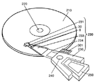
図2は、本発明の薄膜圧電体素子を搭載したアクチュエータ装置をディスクドライブ装置に用いた例を示す模式図である。アクチュエータ装置230は、ディスク210に記録再生を行うヘッド(図示せず)が搭載されたヘッドスライダ231、一対の薄膜圧電体素子8、フレクシャー30、サスペンション233、板バネ部234および支持アーム236から構成されている。なお、サスペンション233、板バネ部234および支持アーム236からアクチュエータアームが構成される。また、フレクシャー30は、スライダ保持部31のヘッド電極パッド32と薄膜圧電体素子8部分の圧電体電極パッド34とからヘッド電極配線33と圧電体電極配線35とが支持アーム236の近傍まで延在されて、外部機器との接続パッド301に接続されている。
【0063】
ヘッドスライダ231はフレクシャー30に支持され、ディスク210に対向する面にヘッド(図示せず)が搭載されている。ヘッドスライダ231の近傍のフレクシャー30上に一対の薄膜圧電体素子8が接着固定されている。
【0064】
フレクシャー30はアクチュエータアームの一部であるサスペンション233に他方の端部が固定されており、サスペンション233は板バネ部234に固定され、さらにこの板バネ部234は支持アーム236に固定されている。
【0065】
支持アーム236は、軸受部240に軸支されており、自由に回転可能である。さらに、支持アーム236には、この支持アーム236を回動させるためのVCMを構成するボイスコイル250が取り付けられている。このボイスコイル250と筐体(図示せず)に固定されたマグネット(図示せず)によりVCMを構成している。したがって、このアクチュエータ装置230は、VCMによる位置決めと一対の薄膜圧電体素子8による位置決めとの2段階による位置決めが可能である。
【0066】
以下、このアクチュエータ装置230を用いたディスクドライブ装置の動作について説明する。ディスク210がスピンドルモータ220により回転駆動されると、ヘッドスライダ231とディスク210との間に空気が流入して空気潤滑膜を形成する。この空気潤滑膜の圧力と板バネ部234からの押圧力とが釣り合った位置で、ヘッドスライダ231が浮上し安定状態となる。この浮上距離は、約10nmから50nmである。このような浮上状態で、ヘッドをディスク210の所定のトラック位置に位置決めするため、支持アーム236がVCMにより回動される。通常のディスクドライブ装置では、このVCMのみで所定のトラック位置に位置決めできる。しかし、さらに高密度の記録を行うためにトラックピッチを微小にする場合、より高精度の位置決めが要求される。これを行うのが一対の薄膜圧電体素子8である。一対の薄膜圧電体素子8は、フレクシャー30のヘッドスライダ231近傍に取り付けられており、この薄膜圧電体素子8を駆動することにより、サスペンション233や支持アーム236とは無関係にヘッドの位置をディスク210の半径方向に数μm程度自由に移動させることができる。すなわち、一対の薄膜圧電体素子8の一方が伸びる方向で、かつ他方が縮む方向に電圧を印加すれば、ディスク210の半径方向(図1に示すY−Y方向)にヘッドを数μm程度移動させることができる。
【0067】
以上のような動作により、VCMによる位置決めと薄膜圧電体素子8による高精度位置決めの2段構成の位置決めができる。なお、このアクチュエータ装置230は、一例であって、特にアクチュエータアームの構造については本実施の形態には限定されない。
【0068】
このような薄膜圧電体素子8の製造方法を図3と図4の製造工程図をもとに説明する。なお、図1に示した構成要素と対応する要素には同一符号を付している。
【0069】
図3(A)は、素子形成基板7上に一対の薄膜圧電体素子8を複数個形成した状態を示す。この図では一対の薄膜圧電体素子8が二対しか示されていないが、具体的には図5に示すように素子形成基板7上には多数の薄膜圧電体素子8が一定の配置構成で形成されている。素子形成基板7としては、MgO基板、Si基板、サファイヤ基板またはチタン酸ジルコン酸鉛単結晶基板等の単結晶基板だけでなく、ステンレス鋼等の金属材料を用いることもできる。
【0070】
薄膜圧電体素子8の作製方法について説明する。素子形成基板7上の二層積層体は、素子形成基板7と同じ基板上に第1電極膜11、圧電体薄膜12および第2電極膜13を積層し、この基板と素子形成基板とを対向させて接着層14により接着した後、一方の基板をエッチング除去し、さらに図1(A)に示すような一方が直角である台形状にフォトリソとエッチング加工すれば得られる。なお、このときに、第2電極膜13の一部が露出するようにビアホールも形成する。その後、絶縁保護膜15を形成し、それぞれの電極膜の一部が露出するようにフォトリソとエッチング加工し、さらに接続電極膜16を形成して図1(A)に示すような形状に加工すれば薄膜圧電体素子8が作製できる。
【0071】
なお、絶縁保護膜15としては、ポリイミドのような有機樹脂膜でもよいし、酸化珪素膜のような無機絶縁膜でもよい。成膜方法としても、塗布法やプラズマ化学気相反応法による成膜あるいはスパッタリングによる成膜等、化学的成膜方法や物理的成膜方法のいずれでもよい。
【0072】
このように薄膜圧電体素子8が形成された面上に、図3(B)に示すように樹脂からなる素子保持膜20を形成する。この素子保持膜20は、衝撃が加わってもクラック等が生じないような柔軟性のある材料で、しかも薄膜圧電体素子8を含む凹凸のある面上にも比較的均一な厚さで形成することが要求される。例えば、ポリアミド樹脂をスピンコートし乾燥させた後、350℃程度の温度でイミド化処理を行って形成したポリイミド膜であってもよいし、ベンゾシクロブテン(BCB)等の有機樹脂を塗布し熱硬化させたBCB膜でもよい。さらに、一般に用いられるフォトレジスト材料、あるいは絶縁樹脂材料で、この後の工程で加えられる温度に耐えることができる材料であれば、素子保持膜20として用いることもできる。素子保持膜20の形成には、スピンコート法のみでなく、霧状にして吹き付ける方法やロールコーティング方法を使用することもできる。また、モノマーを蒸発させ、プラズマ中で重合反応を生じさせて高分子膜を形成する方式で、例えばポリイミド膜やBCB膜を形成して素子保持膜20としてもよい。複数の薄膜圧電体素子8を保持できる強度があれば、その厚さはできるだけ薄いことが望ましいが、ポリイミド樹脂膜の場合には約2〜5μmが適当である。
【0073】
接続電極膜16領域に形成された素子保持膜20の一部をフォトリソとエッチングにより除去して電極パッド18を形成する。これにより、電極パッド18以外が素子保持膜20で覆われた形状が得られる。素子保持膜20に上記の加工を行った後、図3(C)に示すように仮固定用基板5を素子保持膜20が形成された面と対向させ、固定用樹脂6で固定する。さらに、素子形成基板7の薄膜圧電体素子8が形成されていない面の外周部から所定の幅の外周領域7aと素子形成基板7の外周側端部7bまでを含めて、図示するように同様の固定用樹脂6を用いて覆い、保護する。この仮固定用基板5としては、例えばガラス、アルミナ等のセラミック、あるいはリン酸系の薬液に侵されないクロム等をメッキした金属板等を用いることができる。また、固定用樹脂6としては、例えばワックスやフォトレジストを用いればよい。
【0074】
このような形状とした後に、素子形成基板7のみを選択的にエッチングする薬液中に全体を浸漬して、固定用樹脂6で保護されていない素子形成基板7部分をエッチング除去する。例えば、素子形成基板7として、MgO基板を用いる場合には、リン酸系の薬液を用いれば他の材料を侵さずにMgO基板のみを選択的にエッチングできる。また、素子形成基板7として、Si基板を用いる場合には、フッ酸と硝酸の混液を用いれば同様に選択エッチングが可能である。さらに、これらの基板をドライエッチングで除去してもよい。この結果、図3(D)に示すように、素子形成基板7は枠状になり、素子形成基板7側の第1電極膜(図示せず)面が露出した形状が得られる。
【0075】
この状態の基板を用いて、接着樹脂層25をこの第1電極膜(図示せず)面上に形成する。その後、固定用樹脂6を溶解する溶解液中に浸して、固定用樹脂6を溶解させ仮固定用基板5を除去すると、接着樹脂層25が形成された薄膜圧電体素子8が、素子保持膜20と素子形成基板7の外周枠部のみで保持された構造を得ることができる。これを図4(A)に示す。
【0076】
なお、接着樹脂層25は、固定用樹脂6を溶解して仮固定用基板5を除去した後に形成してもよい。また、フレクシャー30面上に形成してもよい。接着樹脂層25としては、例えば、感光性を有し、熱圧着による接着が可能な材料を全面に塗布した後フォトリソとエッチングを行うことで、第1電極膜面上のみに接着樹脂層25を形成する。また、シート状の接着樹脂を薄膜圧電体素子8と同一形状に加工した後、第1電極膜面上に貼り付けて接着樹脂層25としてもよい。あるいは、インクジェット方式で直接第1電極膜面上のみに接着樹脂を塗布して、接着樹脂層25とすることもできる。
【0077】
接着樹脂層25を形成後図4(B)に示すように、ベース40上に載置されたフレクシャー30と薄膜圧電体素子8とを位置合わせし、押圧ツール42に荷重Fを印加して薄膜圧電体素子8の周辺部の素子保持膜20を切断しながらフレクシャー30に薄膜圧電体素子8を熱圧着して接着固定する。接着が完了したら押圧ツール42を薄膜圧電体素子8から離間させ、電極パッド18と圧電体電極パッド34間をワイヤボンディング等の方法でワイヤリード37により接続すれば、図1に示すフレクシャー30に実装された薄膜圧電体素子8が得られる。すなわち、本実施の形態の製造方法では、フレクシャー30上に実装された薄膜圧電体素子8は、電極パッド18が形成される側の面には絶縁保護膜15と樹脂からなる素子保持膜20とが形成されており、この反対面には接着樹脂層25のみが形成されている構成である。
【0078】
この製造方法では、素子形成基板7を除去しても、薄膜圧電体素子8は素子保持膜20により図5に示すような初期の配置形態を保持している。このため、薄膜圧電体素子8を実装用基板であるフレクシャー30に実装するための接着樹脂層25の形成や位置合わせおよび熱圧着工程が確実に、かつ簡単に行うことができるので薄膜圧電体素子8の量産性を大きく向上できる。
【0079】
(第2の実施の形態)
図6は、本発明の薄膜圧電体素子の第2の実施の形態の製造方法の工程を説明するための図であり、図1から図3までに示した構成要素と対応する要素には同一符号を付している。
【0080】
図6(A)は、図3(A)と同様に素子形成基板7上に図1に示した薄膜圧電体素子8を形成した状態を示す。この状態の基板を用いて、図6(B)に示すように、素子形成基板7の外周部で、かつ、薄膜圧電体素子8が形成されていない領域部7cに枠体50を接着剤により固定する。この枠体50としては、素子形成基板7を除去するときの薬液やガス等で侵されない材料であれば良く、例えばステンレス鋼等の金属、ガラス、アルミナ等のセラミック、液晶ポリマー等のプラスチック等を加工して用いることができる。
【0081】
枠体50を素子形成基板7に固定後、この枠体50、薄膜圧電体素子8およびこれらの素子が形成されている素子形成基板7の平面を含む全面に樹脂からなる素子保持膜20を形成する。この素子保持膜20の形成は、第1の実施の形態で説明したと同様な材料、成膜方法で行える。
【0082】
素子保持膜20を形成した後、素子形成基板7のみをエッチングする薬液中に全体を浸漬して、素子形成基板7をすべてエッチング除去すると、薄膜圧電体素子8が素子保持膜20と枠体50のみで保持された形状が得られる。なお、素子形成基板7の除去は薬液によるエッチング除去だけでなく、ドライエッチングでも可能であるし、さらに機械的に研磨して薄くした後にウエットエッチングあるいはドライエッチングしてもよい。
【0083】
この状態で、エッチングにより露出した薄膜圧電体素子8の第1電極膜(図示せず)上に接着樹脂を塗布して、接着樹脂層25を形成する。この接着樹脂層25も第1の実施の形態と同様な材料および作製法を用いることができる。接着樹脂層25までを形成した状態を図6(C)に示す。
【0084】
次に、ベース40上に実装用基板であるフレクシャー30を載置し、薄膜圧電体素子8とフレクシャー30とを位置合わせした後、押圧ツール42により荷重Fを印加しながら加熱してやれば、薄膜圧電体素子8はフレクシャー30に接着固定される。これを図6(D)に示す。押圧ツール42を離間させた後、さらに薄膜圧電体素子8の電極パッド18とフレクシャー30の圧電体電極パッド34とをワイヤボンディング方式によりワイヤリード37で接続すれば、図1に示すようなフレクシャー30上に薄膜圧電体素子8が実装された構成が得られる。
【0085】
なお、圧電体薄膜を形成するために通常使用する素子形成基板7は、MgO基板やSi基板等であり、これらは脆性材料であるので枠状にエッチングして外周枠部を形成すると割れ易い。しかし、本実施の形態で用いる枠体50は素子形成基板7とは別個の基板を用いることができるので、金属のように強度の大きな材料を自由に選択することができる。このため、接着樹脂層25の形成やフレクシャー30への実装時の取り扱いで割れることがなく、これらの工程での歩留まり低下が生じるのを防止できる。
【0086】
なお、本実施の形態では、枠体50は素子形成基板7上の外周部に固定したが、本製造方法はこれに限定されるものではない。例えば、図7に示すように、素子形成基板7の外周に内接するように枠体54を嵌合させて、薄膜圧電体素子8、枠体54の側面部54aおよび素子形成基板7面上に素子保持膜20を被覆してもよい。このような構成とすることで、素子形成基板7をできるだけ広い面積で使用することが可能となり、同時に作製できる薄膜圧電体素子数が多くなり、生産性を向上できる。
【0087】
なお、第1および第2の実施の形態では、薄膜圧電体素子8をフレクシャー30に実装後も素子保持膜20を残存させ、これを保護膜としても利用する構成としたが、本発明はこれに限定されない。素子保持膜20としては、素子形成基板7をエッチング除去したときに薄膜圧電体素子8が保持されればよいので、薄膜圧電体素子8の一部のみに形成するようにして、この一部のみが実装後において残存するようにしてもよい。例えば、電極パッド18を設ける薄膜圧電体素子8の周辺部のみに素子保持膜20を形成してもよいし、さらに数箇所に素子保持膜20を部分的に形成してもよい。すなわち、素子保持膜20による薄膜圧電体素子8の保持はその全面で行う必要はなく、確実に保持されさえすれば部分的であってもよい。一部のみで保持するような形状とするためには、全面に成膜後フォトリソとエッチングで不要部分を除去してもよいし、印刷あるいはインクジェット方式等で所定部分のみに形成してもよい。
【0088】
(第3の実施の形態)
図8(A)は、第3の実施の形態の製造方法により作製した2個の薄膜圧電体素子を一対としてアクチュエータ装置に用いる薄膜圧電体素子の平面図である。図8(B)は、B−B線に沿った断面図で、図8(C)はC−C線に沿った断面図である。この一対の薄膜圧電体素子は、第1の実施の形態と同様に図2に示すディスクドライブ装置に用いることができる。なお、図1から図4までと同様な構成要素については同じ符号を付している。
【0089】
本実施の形態の薄膜圧電体素子80は、それぞれ第1電極膜11と第2電極膜13とで挟まれた圧電体薄膜12からなる2個の積層体10を、それらの第2電極膜13同士を接着層14で接着することによって積層一体化した二層積層体を用いている。この二層積層体の構造および形状については、第1の実施の形態の薄膜圧電体素子8と同じである。
【0090】
本実施の形態の薄膜圧電体素子80は、以下の点が第1の実施の形態の薄膜圧電体素子8と異なる。第1は、第1電極膜11と第2電極膜13とを外部機器に接続するための接続電極膜16を形成する領域のみに絶縁保護膜150が形成されていることである。図8(A)から(C)よりわかるように、絶縁保護膜150は接続電極膜16の形成領域には形成されているが、それ以外の領域には形成されていない。
【0091】
第2は、薄膜圧電体素子80の接続電極膜16が形成される領域を除く領域が圧電体として機能する領域であるが、この領域には樹脂からなる素子保持膜20と、この素子保持膜20と同じ材料で同じ厚さに形成した樹脂保護膜200が形成されていることである。
【0092】
第3は、薄膜圧電体素子80の接続電極膜16形成領域近傍の隙間部分と先端近傍の隙間部分とに素子保持膜20と樹脂保護膜200とからなる素子間連結部201、202が形成されて、薄膜圧電体素子80間が連結されていることである。
【0093】
第4は、薄膜圧電体素子80が素子保持膜20と樹脂保護膜200とからなる保持連結部203、204、205が実装後に切断されて、その一部が残された状態となっていることである。
【0094】
以下、このような薄膜圧電体素子80構造を作製するための製造方法について、特に第1の実施の形態と異なる工程を主体に説明する。第1の実施の形態で説明した二層積層体10を図8に示すような形状に加工後、絶縁保護膜150が接続電極膜16の形成される領域のみとなるように所定のパターン加工を行い、さらに接続電極膜16を形成する。このようなプロセスは、一般的な成膜、パターン形成技術で加工することができるので、詳しい説明は省略する。
【0095】
このような形状とした後、第1の実施の形態の製造方法と同様に全面に樹脂からなる素子保持膜20を形成し、固定用樹脂を用いて仮固定用基板を貼り合わせ、薄膜圧電体素子80が形成されている領域の素子形成基板7をエッチング除去した後、固定用樹脂を溶解させれば素子形成基板7の外周枠部と素子保持膜20とで保持された構造が得られる。次に、素子形成基板7をエッチングして露出した第1電極膜11を含む面上に素子保持膜20と同じ材料を用いて、同じ厚さとなるように樹脂保護膜200を形成する。これを図9に示す。
【0096】
素子保持膜20と樹脂保護膜200を形成後、一対の薄膜圧電体素子80間を連結する素子間連結部201、202と、薄膜圧電体素子80を素子保持膜20と樹脂保護膜200とで保持するための保持連結部203、204、205を形成する。これは、通常のフォトリソ、エッチングプロセスにより行うことができる。これらの加工を行うときに、接続電極膜16上に形成された素子保持膜20の一部をエッチングして露出させて、電極パッド18を形成する。この加工を行った状態を図10と図11に示す。図10(A)は、図8(A)と同じ断面部分であり、図10(B)は、図8(B)と同じ断面部分を示す。また、図11は、素子形成基板7の外周枠部、素子保持膜20および素子保護膜200で複数の薄膜圧電体素子が連結されている平面形状を示す。
【0097】
このような形状とすることにより、実装用基板であるフレクシャー30に実装するとき、押圧ツール42で保持連結部203、204、205のみを打ち抜いて切断すればよいので、押圧ツール42が誤って薄膜圧電体素子80に接触して損傷させることがない。また、圧電体として機能する領域部の両表面に同じ材料で、かつ同じ厚さの膜が形成されるので、これらの膜によるそりはキャンセルされて生じず、圧電体特性を劣化させることが少ない。
【0098】
なお、本実施の形態では、薄膜圧電体素子80をフレクシャー30に接着する接着樹脂層25は、フレクシャー30側に形成する方が作業性としては良好であるが、インクジェット形成等により薄膜圧電体素子80側に形成することも可能である。
【0099】
(第4の実施の形態)
図12は、本発明の薄膜圧電体素子の第4の実施の形態の製造方法を示す工程説明図である。なお、図1から図3に示した構成要素と対応する要素には同一符号を付している。
【0100】
図12(A)は、第1の実施の形態の製造方法で説明したものと同じ構造であり、素子形成基板7上に薄膜圧電体素子8が形成された状態を示す。
【0101】
この素子形成基板7の薄膜圧電体素子8が形成された面に可撓性基板56を押し当てて、粘着固定する。このときに、可撓性基板56単独では曲がりやしわが発生し易いので、これを防止するため枠体52をこの可撓性基板56に固定して、可撓性基板56に張力が加わった状態としておいてから貼り付けることが望ましい。このようにして貼り付けた状態を図12(B)に示す。
【0102】
なお、図12(B)では枠体52が素子形成基板7に嵌合するようにしているが、本実施の形態の製造方法ではこのような嵌合状態は必須ではなく、適当に隙間があっても特に問題はない。複数の薄膜圧電体素子8が可撓性基板56に粘着しており、可撓性基板56の強度が大きいので、素子形成基板7を枠体52で必ずしも保持する必要がないためである。
【0103】
この状態で素子形成基板7のみをエッチングする薬液に全体を浸して、素子形成基板7をエッチング除去し、それにより露出した薄膜圧電体素子8の第1電極膜(図示せず)面に接着樹脂を塗布して、接着樹脂層25を形成する。これを図12(C)に示す。この接着樹脂層25も、第1の実施の形態の製造方法で説明した材料および成膜方法を用いることができる。
【0104】
次に、図12(D)に示すように、ベース40上に載置したフレクシャー30と薄膜圧電体素子8とを位置合わせして、押圧ツール42を加圧、加熱すれば、薄膜圧電体素子8はフレクシャー30と接着固定される。このときに、可撓性基板56に形成されている粘着層が紫外線照射により粘着性を低下する性質を有したものを用いれば、押圧ツール42で加圧、加熱すると同時に紫外線照射をすることで、非常に容易に、かつ、確実に可撓性基板56から薄膜圧電体素子8を剥離することができる。例えば、このような可撓性基板56としては、半導体をダイシングするときに用いる粘着性を有したフィルム等を利用することもできる。
【0105】
このようにして、薄膜圧電体素子8がフレクシャー30上に接着固定された状態を図12(E)に示す。第4の実施の形態では、第1、第2および第3の実施の形態の製造方法の場合と異なり素子保持膜が不要であるので、この膜の形成やパターン加工工程を省略することができる。また、素子形成基板7をエッチング除去した後の薄膜圧電体素子8は可撓性基板56で保持されるが、この可撓性基板56は50μm程度の厚さにできるので、作業性が非常に良好である。
【0106】
なお、第1の実施の形態から第4の実施の形態までは、一対の薄膜圧電体素子を例として製造方法を説明したが、本発明の製造方法はこれに限定されるものではなく、薄膜圧電体素子が1個のみで用いるような構成でもよい。さらに、アクチュエータ装置としての応用のみでなく、薄膜圧電体素子を用いて変位量を測定するセンサ等も同様の製造方法を用いれば、容易にかつ歩留まりよく製造できる。
【0107】
また、薄膜圧電体素子として、第1電極膜と第2電極膜とで挟まれた圧電体薄膜を二層積層する構成で説明したが、特にこの構成に限定されるものではなく、一層のみでも同様な製造方法で製造することができる。
【0108】
また、第1、第2および第4の実施の形態では、薄膜圧電体素子の第1電極膜面上に直接接着樹脂層を形成する工法について説明したが、本発明はこれに限定されない。すなわち、接着樹脂層を形成する前に絶縁性の保護膜をあらかじめ形成し、所定のパターン加工を行った後に接着樹脂層を形成するようにしてもよい。このようにして、第1電極膜を含む薄膜圧電体素子に絶縁性の保護膜を形成することで、耐湿性の改善やゴミ等の発生の防止がより確実に行える。
【0109】
さらに、第1および第2の実施の形態ではフレクシャーに薄膜圧電体素子を実装後に素子保持膜が全く残存しないようにすることも本発明の範囲内で可能である。すなわち、素子保持膜を形成する樹脂材料として、例えば熱可塑性接着剤を用いれば、フレクシャーに薄膜圧電体素子を接着後にイソプロパノール等の溶剤でこの熱可塑性接着剤を溶解除去できる。これを溶解除去することによって、実装後の状態で素子保持膜が残存しないようにすることもできる。また、例えば、200℃、1分以上の加熱で接着特性が低下するような接着樹脂を用いることもできる。この接着樹脂を用いて素子保持膜を形成すれば、フレクシャーに薄膜圧電体素子を接着するときの加熱により、素子保持膜の接着性を低下させて薄膜圧電体素子から素子保持膜を簡単に剥離させることができる。さらに、紫外線照射により粘着性が低下する材料を素子保持膜として塗布形成し、実装時に紫外線を照射しながら加熱、加圧することで、素子保持膜を薄膜圧電体素子から除去する方法でもよい。このように実装後に素子保持膜が残存しないようにすれば、薄膜圧電体素子の接続電極膜上に形成された素子保持膜を除去して電極パッドを形成する工程が不要となるので、工数の削減にもなる。
【0110】
【発明の効果】
以上説明したように本発明の薄膜圧電体素子の製造方法は、第1電極膜、圧電体薄膜および第2電極膜をこの順に積層してなる平板状の積層体、またはこの積層体の第2電極膜同士を対向させて積層した二層積層体を素子形成基板上に形成し、所定の接続電極部を設けてなる薄膜圧電体素子を素子形成基板の一方の面上に複数個形成し、これらの薄膜圧電体素子を含んで素子形成基板の一方の面上に樹脂からなる素子保持膜を被覆し、薄膜圧電体素子が形成されている領域の素子形成基板を除去することで薄膜圧電体素子を素子保持膜で保持させて、複数の薄膜圧電体素子の初期の配置が保持されるようにした方法である。
【0111】
これにより、接着樹脂層の形成や保護膜の形成が複数の薄膜圧電体素子に対して同時に一括して形成できる。また、薄膜圧電体素子を実装用基板上に位置合わせして実装する場合に、量産性よく、かつ、高精度に行うことが可能であるという大きな効果が得られる。
【0112】
また、本発明の薄膜圧電体素子は、平板状の薄膜圧電体素子の圧電体として機能する領域の両表面に、樹脂からなる素子保持膜と、この素子保持膜と同じ材料で同じ厚さの樹脂保護膜とを形成した構成からなる。さらに、これらからなる2個の薄膜圧電体素子を素子保持膜と樹脂保護膜とで連結して一体化した構成としてアクチュエータ装置用としたものである。
【0113】
これにより、薄膜圧電体素子の圧電体として機能する領域の両表面が、同じ材料で同じ厚さの素子保持膜と樹脂保護膜とで形成されているので、そりが生じず圧電体特性が低下しない。また、全体が樹脂からなる素子保持膜と樹脂保護膜とにより保護されるので、薄膜圧電体素子の腐食やゴミの発生を防止でき、アクチュエータ装置として使用するときの信頼性が大きく向上するという大きな効果が得られる。
【図面の簡単な説明】
【図1】(A)は、本発明の第1の実施の形態の製造方法により作製した薄膜圧電体素子部分の平面図
(B)は、X−X線に沿った断面図
【図2】本発明の薄膜圧電体素子を搭載したアクチュエータ装置を用いたディスクドライブ装置の例を示す模式図
【図3】本発明の薄膜圧電体素子の第1の実施の形態の製造方法の主要工程を示す工程説明図
【図4】同実施の形態の製造方法の主要工程を示す工程説明図
【図5】同実施の形態の製造方法で、薄膜圧電体素子を素子形成基板上に複数個形成した状態を示す図
【図6】本発明の薄膜圧電体素子の第2の実施の形態の製造方法の主要工程を示す工程説明図
【図7】同実施の形態の製造方法の変形例の主要工程を示す図
【図8】(A)は、本発明の第3の実施の形態の製造方法により作製した薄膜圧電体素子の平面図
(B)は、同薄膜圧電体素子のB−B線に沿った断面図
(C)は、同薄膜圧電体素子のC−C線に沿った断面図
【図9】本発明の薄膜圧電体素子の第3の実施の形態の製造方法の主要工程を示す工程説明図
【図10】同実施の形態の製造方法の主要工程を示す工程説明図
【図11】同実施の形態の製造方法で、薄膜圧電体素子を素子保持膜と樹脂保護膜とで保持した状態を示す平面図
【図12】本発明の薄膜圧電体素子の第4の実施の形態の製造方法を示す工程説明図
【符号の説明】
5 仮固定用基板
6 固定用樹脂
7 素子形成基板
7a 外周領域
7b 外周側端部
7c 領域部
8,80 薄膜圧電体素子
10 積層体
11 第1電極膜
12 圧電体薄膜
13 第2電極膜
14 接着層
15,150 絶縁保護膜
16 接続電極膜
18 電極パッド
20 素子保持膜
25 接着樹脂層
30 実装用基板(フレクシャー)
31 スライダ保持部
32 ヘッド電極パッド
33 ヘッド電極配線
34 圧電体電極パッド
35 圧電体電極配線
37 ワイヤリード
40 ベース
42 押圧ツール
50,52,54 枠体
54a 側面部
56 可撓性基板
200 樹脂保護膜
201,202 素子間連結部
203,204,205 保持連結部
210 ディスク
220 スピンドルモータ
230 アクチュエータ装置
231 ヘッドスライダ
233 サスペンション
234 板バネ部
236 支持アーム
240 軸受部
250 ボイスコイル
301 接続パッド[0001]
BACKGROUND OF THE INVENTION
The present invention relates to a thin film piezoelectric element used for micropositioning or as a piezoelectric sensor, a manufacturing method thereof, and an actuator device using the same.
[0002]
[Prior art]
In recent years, along with the advancement of semiconductor technology, efforts have been made to make micromachines using semiconductor manufacturing technology and greatly reduce the size of various mechanisms, and mechanical electrical elements such as microactuators using such technology. Is in the limelight. Such an element can realize a small and highly accurate mechanical mechanism part, and can greatly improve the productivity by using a semiconductor process. In particular, a microactuator using a piezoelectric element is applied to minute displacement of a scanning tunnel microscope, minute positioning of a head slider of a magnetic disk recording / reproducing apparatus (hereinafter referred to as a disk drive apparatus), and the like.
[0003]
For example, in a disk drive device, a magnetic head for recording / reproducing information on / from a magnetic disk is mounted on a head slider and attached to an actuator arm. The actuator arm is swung by a voice coil motor (hereinafter referred to as VCM) to be positioned at a predetermined track position on the magnetic disk, and recording / reproduction is performed by the magnetic head. However, with the improvement in recording density, sufficient accuracy cannot be ensured by positioning using such a conventional VCM alone. For this reason, in addition to the VCM positioning means, there has been proposed a technique for performing high-speed, high-precision positioning by micro-driving the head slider by micro-positioning means using piezoelectric elements (for example, non-patent literature). 1).
[0004]
Various applications of the piezoelectric element including the actuator as described above are expected. However, conventionally, it has often been formed by a green sheet lamination method or a thick film multilayer formation method. This is because the above-described manufacturing method is inexpensive, can be laminated relatively easily, and can increase the amount of displacement. However, since the thickness of one layer of the piezoelectric element manufactured by these manufacturing methods is about several tens of μm, a driving voltage of about 100 V is required.
[0005]
On the other hand, in order to realize a small displacement, a low voltage drive, and a large displacement, a method of similarly laminating by a thin film forming method has also been proposed (for example, see Patent Document 1). A piezoelectric element formed by such a thin film manufacturing method needs to be used after being formed on a substrate such as a silicon single crystal substrate and performing various processes, and then finally used as a piezoelectric element. There are often. If the substrate is removed and the piezoelectric elements are used alone, they are thin, so that it is very difficult to mount them on the piezoelectric substrate without causing damage, and there is a big problem in mass productivity.
[0006]
In view of such points, a manufacturing method has been shown in which a pyroelectric element and a piezoelectric element are separately mounted on an electrode-formed substrate with high productivity (see, for example, Patent Document 2). According to this, an element transfer jig is prepared, and after the elements formed on the temporary substrate are bonded to the element transfer jig in a predetermined arrangement with resin or double-sided adhesive tape, only the temporary substrate is selectively selected. Etch. Next, the electrode provided on the electrode forming substrate and the electrode of the element are bonded to face each other, and bonded by, for example, soldering. Thereafter, a pyroelectric element or a piezoelectric element joined in a predetermined shape on the electrode forming substrate by dissolving and removing the resin or adhesive tape or the like adhering the element and separating the element from the element transfer jig Is formed. Since the element is bonded and fixed on the element transfer jig, the element is not deformed or damaged even if the temporary substrate is selectively etched away, and the predetermined arrangement state can be maintained. Can be pasted together.
[0007]
In addition, after the pyroelectric thin film on which the organic thin film is formed is adhered to the substrate provided with the opening, the pyroelectric thin film is held only by the organic thin film by etching away the substrate on which the pyroelectric thin film is formed. The structure is shown (see, for example, Patent Document 3). With such a structure, thermal separation between elements is easy, manufacturing man-hours can be reduced, and mass productivity is improved.
[0008]
[Patent Document 1]
JP-A-8-88419
[Patent Document 2]
Japanese Patent Laid-Open No. 11-345833
[Patent Document 3]
JP-A-4-170077
[Non-Patent Document 1]
Ultra-high TPI and piggyback actuator (IDEMA Japan News No.32, pp4-7, published by International Disk Drive Association)
[0009]
[Problems to be solved by the invention]
In the above-mentioned Patent Document 2, elements in a state where the temporary substrates are individually separated are bonded onto an element transfer jig. However, in the method of bonding elements one by one in this way, it is difficult to increase the bonding accuracy between the elements. In other words, the smaller the element is, the greater the number of electrode terminals, and the greater the number of elements to be bonded on the element transfer jig, the more the gap between the plurality of elements bonded on the electrode forming substrate and the element transfer jig. The influence of misalignment becomes large, and this makes alignment difficult. In addition, the adhesive layer is required to be a material that can withstand the soldering mounting temperature and be a material that can be removed by a chemical solution even after receiving the temperature.
[0010]
Furthermore, in Patent Document 3, an organic thin film is formed so as to cover a pyroelectric thin film formed on a predetermined substrate, and then adhered to a polyimide substrate provided with an opening, and then the substrate on which the pyroelectric thin film is formed is attached. This is a method of manufacturing a pyroelectric infrared detector having a structure in which the pyroelectric thin film is held only by the organic thin film at the opening by etching away. Also in the case of this manufacturing method, only the substrate on which the pyroelectric thin film is formed on the mounting substrate such as a polyimide substrate is adhered, and then only this substrate is removed by etching. That is, since the substrate on which the pyroelectric thin film is formed is etched after mounting, the mounting substrate and the wiring electrode are altered by the chemical solution or gas for the etching, and the shape of the mounting substrate is limited. The problem of receiving also arises.
[0011]
The present invention provides a structure in which a thin film piezoelectric element is formed on an element forming substrate using thin film technology, and the thin film piezoelectric element is held by the element holding film even after the element forming substrate is removed by etching. An object of the present invention is to provide a thin film piezoelectric element manufacturing method and a thin film piezoelectric element with good mass productivity including the mounting process so that the thin film piezoelectric element maintains the initial arrangement state until the process.
[0012]
[Means for Solving the Problems]
In order to solve this problem, a method of manufacturing a thin film piezoelectric element according to the present invention includes a flat laminate formed by laminating a first electrode film, a piezoelectric thin film, and a second electrode film in this order, A two-layer laminated body in which the second electrode films are laminated to face each other is formed on an element forming substrate, and a plurality of thin film piezoelectric elements each having a predetermined connection electrode film are formed on one surface of the element forming substrate. The thin film piezoelectric element is formed by covering the element holding film on one surface of the element forming substrate including these thin film piezoelectric elements and removing the element forming substrate in the region where the thin film piezoelectric element is formed. Is held by the element holding film, and then the thin film piezoelectric element held by the element holding film is separated individually or in predetermined units.
[0013]
In addition, the thin film piezoelectric element of the present invention has an element holding film made of resin on the both surfaces of a region functioning as a piezoelectric body of a flat thin film piezoelectric element, and the same material and the same thickness as the element holding film. The structure is formed with a resin protective film, and two thin film piezoelectric elements composed of these are connected and integrated by an element holding film and a resin protective film, and are used for an actuator device.
[0014]
With this manufacturing method, the plurality of thin film piezoelectric elements formed on the element formation substrate are maintained in the initial arrangement state by the outer peripheral frame and the element holding film even if the element formation substrate is removed by etching or the like. The For this reason, a resin protective film and an adhesive resin layer can be simultaneously formed on the plurality of thin film piezoelectric elements at the same time, and photolithography and etching of these films can be easily performed. In addition, when mounting thin film piezoelectric elements by aligning them on a piezoelectric substrate, it is possible to carry out mass production with high accuracy using an automatic mounting machine because the arrangement pitch is constant. is there.
[0015]
Further, since the thin film piezoelectric elements formed in a pair are connected by the element holding film, the accuracy and mass productivity when mounted on the piezoelectric body mounting substrate can be improved. In addition, since both surfaces of the region functioning as the piezoelectric body of the thin film piezoelectric element are formed of the same material and the same thickness of the element holding film and the resin protective film, warpage does not occur and the piezoelectric characteristics do not deteriorate. . In addition, since the whole is protected by the element holding film made of resin and the resin protective film, corrosion of the thin film piezoelectric element and generation of dust can be prevented, and the reliability when used as an actuator device is greatly improved.
[0016]
DETAILED DESCRIPTION OF THE INVENTION
The method for manufacturing a thin film piezoelectric element of the present invention includes a flat laminate formed by laminating a first electrode film, a piezoelectric thin film, and a second electrode film in this order, or the second electrode films of this laminate are opposed to each other. Forming a plurality of thin film piezoelectric elements each having a predetermined connection electrode film on one surface of the element forming substrate; and forming the thin film piezoelectric body. The element holding film made of resin is coated on one surface of the element forming substrate including the element, and the element forming substrate in the region where the thin film piezoelectric element is formed is removed to remove the thin film piezoelectric element from the element holding film. And a step of separating the thin film piezoelectric element held by the element holding film individually or every predetermined unit.
[0017]
By this manufacturing method, the plurality of thin film piezoelectric elements are held by the element holding film even if the element forming substrate is removed, so that the initial arrangement state is held. Therefore, it is possible to easily form an adhesive resin layer simultaneously on a plurality of thin film piezoelectric elements, or process by photolithography and etching.
[0018]
In the method for manufacturing a thin film piezoelectric element of the present invention, the step of holding the thin film piezoelectric element with the element holding film includes an element holding film made of resin on one surface of the element forming substrate including the thin film piezoelectric element. The element forming substrate coated with the element holding film is bonded and fixed to the temporary fixing substrate with a fixing resin so that one surface of the element forming substrate is opposed to the temporary fixing substrate, and opposite to the one surface of the element forming substrate. After covering the outer peripheral region of a predetermined width from the outer peripheral portion of the surface and the outer peripheral side end portion of the element forming substrate with the fixing resin, the device forming substrate other than the region covered with the fixing resin is etched away. .
[0019]
By using such a manufacturing method, it is possible to easily produce a frame by selectively removing only the region where the thin film piezoelectric element of the element formation substrate is formed. By producing the frame, it is possible to prevent the element holding film holding the thin film piezoelectric element from being bent or wrinkled. As this etching, it may be immersed in a chemical solution that dissolves the element formation substrate and removed by etching, or may be performed by dry etching.
[0020]
In the method for manufacturing a thin film piezoelectric element of the present invention, the step of holding the thin film piezoelectric element with the element holding film includes an element holding film made of resin on one surface of the element forming substrate including the thin film piezoelectric element. And shielding the area where the thin film piezoelectric element is not formed with a mask made of a material that is not etched in the atmosphere in which the element forming substrate is etched. And a method of removing the element forming substrate region not shielded by the mask by dry etching.
[0021]
With such a manufacturing method, when performing selective etching to leave the outer periphery of the element forming substrate in a frame shape, it is not necessary to use a temporary fixing substrate or a fixing resin, so that the process is simplified, and the thin film A structure in which the piezoelectric element is held by the element holding film and the outer peripheral frame portion can be realized.
[0022]
For example, when a magnesium oxide single crystal substrate (hereinafter referred to as an MgO substrate) is used as the element formation substrate, the mask material is stainless steel, chromium, copper, or a metal such as copper or iron plated with chromium, glass or Using ceramics such as alumina, these can be made into a frame shape and adhered to the element formation substrate for dry etching. Alternatively, these materials may be formed by sputtering or the like, the film on the surface of the element formation substrate to be etched may be removed by etching, and other portions may be left in a frame shape to serve as a mask. For example, when a silicon single crystal substrate (hereinafter referred to as an Si substrate) is used as an element formation substrate, a metal such as aluminum or a ceramic material such as alumina is used, and only these frame-shaped portions that do not etch the Si substrate are used. A film may be formed as a mask.
[0023]
Further, in the method of manufacturing the thin film piezoelectric element of the present invention, the step of holding the thin film piezoelectric element with the element holding film is performed on the region where the thin film piezoelectric element is not formed on the outer periphery of the element forming substrate. An element made of resin on one surface of the element forming substrate, including a thin film piezoelectric element and a side end portion of the frame body, in which a frame surrounding the thin film piezoelectric element is fixed on one surface of the forming substrate. After covering the holding film, the device forming substrate is selectively removed.
[0024]
By this manufacturing method, various materials such as a metal material, a ceramic material, or glass can be used as the frame. If a metal material is used, various processes necessary for securing the strength of the frame can be easily performed. For example, if a step is provided on the surface of the frame body fixed to the element formation substrate, the width of the entire frame body can be increased while reducing the width of the frame body to be fixed to the element formation substrate. With such a structure, the width for fixing to the element formation substrate can be reduced while sufficiently securing the strength as a frame, so the number of thin film piezoelectric elements that can be fabricated on the element formation substrate can be increased. Mass productivity can be improved. Further, it is not necessary to use a temporary fixing substrate, and the manufacturing process can be simplified. The element formation substrate is removed by wet etching immersed in a chemical solution, dry etching performed in a reaction gas, or mechanical polishing to a predetermined thickness to make a thin plate and then etching with a chemical solution or dry etching. Can be done.
[0025]
In the method for manufacturing a thin film piezoelectric element of the present invention, the step of holding the thin film piezoelectric element with the element holding film is a process of fitting the frame body to the element forming substrate so that the outer periphery of the element forming substrate is inscribed. And an element holding substrate made of resin on one surface of the element forming substrate including the thin film piezoelectric element and the side edges of the frame, and then selectively removing the element forming substrate.
[0026]
With this manufacturing method, it is possible to manufacture the thin film piezoelectric element up to the vicinity of the outer peripheral portion of the element forming substrate, and the number of piezoelectric elements that can be formed on the element forming substrate can be increased, so that mass productivity can be improved. Furthermore, since the frame only needs to be fitted to the outer peripheral portion of the element forming substrate, the manufacturing process is simplified. The element forming substrate can be removed by being immersed in a chemical solution, or by dry etching, or by mechanical polishing to a predetermined thickness together with the frame, and then etching with the chemical solution. Alternatively, dry etching may be used. Further, when the frame body is fitted to the element formation substrate, it is desirable that the element formation substrate surface and the frame body surface be substantially the same surface. However, the surface of the frame body and the surface of the element forming substrate can be used as long as they can be coated with an adhesive resin layer and formed with an insulating protective film after fitting, or a photolithography and etching process for processing them into a predetermined pattern shape. May not be coplanar.
[0027]
Further, in the method for manufacturing a thin film piezoelectric element according to the present invention, the step of separating the thin film piezoelectric element held by the element holding film individually or in predetermined units includes a mounting substrate for mounting the thin film piezoelectric element. And the surface opposite to the surface on which the connection electrode film is formed, apply a pressing force to the thin film piezoelectric element to move the thin film piezoelectric element together with the element holding film to the mounting substrate surface, It consists of a method of adhering and fixing to a mounting substrate with an adhesive resin layer.
[0028]
With this manufacturing method, the initial arrangement state is maintained even when the thin film piezoelectric element is mounted on the mounting substrate, so that highly accurate alignment is easy and the piezoelectric element is less likely to be damaged. Mass production and yield can be greatly improved.
[0029]
The method for manufacturing a thin film piezoelectric element of the present invention comprises a method in which a step of dissolving and removing the element holding film with a dissolving solution after the thin film piezoelectric element is bonded and fixed to the mounting substrate is further added. When the element holding film remains in the thin film piezoelectric element separated from the element forming substrate, the element holding film protects the thin film piezoelectric element against moisture resistance and suppresses the generation of dust from the thin film piezoelectric element. At the same time, it acts to suppress the displacement of the thin film piezoelectric element. By this manufacturing method, the element holding film can be finally dissolved and removed to prevent the displacement amount of the thin film piezoelectric element from being lowered.
[0030]
In the method of manufacturing a thin film piezoelectric element of the present invention, the element holding film has a characteristic that the adhesiveness is lowered by heating or ultraviolet irradiation, and when the thin film piezoelectric element is bonded and fixed to the mounting substrate or after that, The method further includes a step of further separating the thin film piezoelectric element by heating or irradiating with ultraviolet rays to reduce adhesion.
[0031]
By adding a step of separating the element holding film from the thin film piezoelectric element using the element holding film having such material characteristics, it is possible to prevent the displacement amount of the thin film piezoelectric element from being lowered. Since the element holding film separation step is a dry process without using a chemical solution, it can be easily performed even after the thin film piezoelectric element is bonded to the mounting substrate, and no new equipment is required. As such an element holding film, for example, a thermoplastic adhesive having a thermal decomposition temperature of 200 ° C. is used, and if it is heated to the above temperature after mounting, the adhesiveness is lowered. Can be peeled off.
[0032]
The method for producing a thin film piezoelectric element of the present invention comprises a method of applying a liquid organic resin as an element holding film and drying and curing it.
[0033]
By this manufacturing method, a relatively uniform and thin resin film can be formed on the surface of the element forming substrate including the thin film piezoelectric element. In addition, since the organic resin film is flexible, not only is it difficult to break, but even if the element holding film is left after mounting the thin film piezoelectric element on the mounting substrate, the influence on the decrease in the displacement amount of the thin film piezoelectric element Less is. As the organic resin film, any material can be used as long as it can withstand a heating temperature of about 200 ° C. required after this step, such as polyimide, photoresist, rubber-based resin, or thermoplastic adhesive.
[0034]
The method for manufacturing a thin film piezoelectric element of the present invention comprises a method of forming an organic resin film by plasma polymerization as an element holding film.
[0035]
By this manufacturing method, the element holding film can be uniformly formed on the surface of the element forming substrate including the thin film piezoelectric element. In particular, this method does not cause an increase in thickness at the concave portion, which tends to occur when applying a liquid resin material, or a decrease in thickness at the convex portion, and can be uniformly formed in any place. Even if it is thin, an element holding film having a stable strength can be formed. As this organic resin film, a polyimide thin film obtained by evaporating two or more monomers and polymerizing on the substrate, or a thin film prepared by evaporating a polymer and introducing it into a plasma to cause a polymerization reaction, such as polyimide and benzo Cyclobutene (BCB) or the like can be used.
[0036]
The thin film piezoelectric element manufacturing method of the present invention includes a flat laminate formed by laminating the first electrode film, the piezoelectric thin film, and the second electrode film in this order, or the second electrode films of the laminate. A plurality of thin films formed by forming a two-layer laminate on the element formation substrate and providing connection electrode films for electrically connecting the first electrode film and the second electrode film to an external device The step of forming the piezoelectric element on one surface of the element forming substrate and the one surface of the element forming substrate on which the thin film piezoelectric element is formed are bonded to the flexible substrate having the adhesive surface. A step of selectively removing the element formation substrate to hold the thin film piezoelectric element by a flexible substrate, and a step of separating the thin film piezoelectric element held by the flexible substrate individually or in predetermined units The method which has these.
[0037]
By this manufacturing method, the plurality of thin film piezoelectric elements are held by the flexible substrate even if the element forming substrate is removed by etching, so that the initial arrangement state is maintained. Therefore, it is possible to easily form an adhesive resin layer simultaneously on a plurality of thin film piezoelectric elements, or process by photolithography and etching.
[0038]
Further, in the method of manufacturing the thin film piezoelectric element of the present invention, the step of separating the thin film piezoelectric element held by the flexible substrate individually or every predetermined unit is performed by applying ultraviolet rays as the flexible substrate. Thin film on the mounting substrate with the mounting substrate for bonding and fixing the thin film piezoelectric element and the surface of the thin film piezoelectric element opposite to the connection electrode film forming surface facing each other using a material with reduced performance When the piezoelectric element is bonded and fixed, the thin film piezoelectric element is peeled from the flexible substrate by heating the thin film piezoelectric element and applying a pressing force while irradiating the flexible substrate with ultraviolet rays. It consists of the method of adhering and fixing to.
[0039]
With this manufacturing method, since the thin film piezoelectric element can be easily separated from the flexible substrate, the work process for bonding and fixing the thin film piezoelectric element to the mounting substrate can be simplified.
[0040]
In the state where the element formation substrate is removed and only the thin film piezoelectric element is held on the flexible substrate, the distance between the thin film piezoelectric elements can be increased by uniformly extending the flexible substrate from the outer peripheral portion. It is also possible to use a flexible substrate. If such a flexible substrate is used, the workability of the pressing tool when the thin film piezoelectric element is bonded onto the mounting substrate can be improved. As such a flexible substrate, for example, it is possible to use a film having adhesiveness to be pasted when a semiconductor substrate is diced, and further, only such a film is used to form an element on this film. It is also possible to apply an adhesive that can withstand a chemical solution for etching the substrate.
[0041]
The method of manufacturing a thin film piezoelectric element according to the present invention includes a resin protective film having the same material and thickness as the element holding film on the surface of the thin film piezoelectric element including the first electrode film exposed by removing the element forming substrate. It consists of the method of forming.
[0042]
With this manufacturing method, in the region where the thin film piezoelectric element functions as a piezoelectric body, films of the same material and the same thickness are formed on both surfaces, so that warpage does not occur and environmental resistance, particularly moisture resistance Can be improved. This resin protective film can be easily produced by the same method as the element holding film.
[0043]
Furthermore, in the method for manufacturing a thin film piezoelectric element of the present invention, two thin film piezoelectric elements are configured as a pair, and at least a part of the pair of thin film piezoelectric elements is connected by the element holding film after being separated from the element holding film. It consists of the method of producing.
[0044]
With this manufacturing method, a large amount of displacement can be obtained when used as an actuator device. Also, by using adjacent thin film piezoelectric elements as a pair, variation in characteristics between these thin film piezoelectric elements can be reduced, and a stable operation as an actuator device can be achieved.
[0045]
Furthermore, the thin film piezoelectric element of the present invention includes a flat laminate in which a first electrode film, a piezoelectric thin film, and a second electrode film are laminated in this order, and the first electrode film and the second electrode film are electrically connected to an external device. A connection electrode film formed at one end of one surface of the laminate, and an element holding film made of resin on one surface of the laminate on which the connection electrode film is formed, and an element on the other surface A resin protective film having the same material and thickness as the holding film is formed.
[0046]
With this configuration, an element holding film and a resin protective film having the same material and thickness are formed on both surfaces of a region functioning as a piezoelectric body in a flat laminate, so that no warpage occurs and stable In addition to obtaining excellent piezoelectric characteristics, it is possible to improve moisture resistance and suppress dust generation.
[0047]
Furthermore, the thin film piezoelectric element of the present invention is a flat two-layer laminate in which the second electrode films of the laminate in which the first electrode film, the piezoelectric thin film, and the second electrode film are laminated in this order are laminated to face each other. A connection electrode film formed at one end of one surface of the two-layer laminate for electrically connecting the first electrode film and the second electrode film to an external device, and two connection electrode films formed An element holding film made of resin is formed on one surface of the layered laminate, and a resin protective film having the same thickness and the same material as the element holding film is formed on the other surface.
[0048]
With this configuration, since the element holding film and the resin protective film having the same thickness as the same material are formed on both surfaces of the region functioning as the piezoelectric body of the flat plate-like two-layer laminate, no warpage occurs. Not only can stable piezoelectric characteristics be obtained, but also improvement in moisture resistance and generation of dust can be suppressed. Further, since the two piezoelectric thin films are laminated, the displacement characteristics of the thin film piezoelectric element can be greatly improved.
[0049]
Further, the thin film piezoelectric element of the present invention comprises two thin film piezoelectric elements as a pair, and the pair of thin film piezoelectric elements is arranged on the same plane with a predetermined gap in the length direction. And a configuration in which the thin film piezoelectric element is connected by forming an element holding film and a resin protective film in at least a part of the gap, and having a symmetrical shape with respect to a line passing through the center of the gap. Have
[0050]
With this configuration, since the element holding film and the resin protective film having the same material and the same thickness are formed on both surfaces of the region functioning as the piezoelectric body of the flat plate-like laminate, no warpage occurs and stable. Not only can piezoelectric characteristics be obtained, but also moisture resistance can be improved and dust generation can be suppressed. Furthermore, since it has a symmetrical shape with respect to the line segment in the length direction and is connected by an element holding film, even when it is adhesively fixed on a mounting substrate, a positional deviation between thin film piezoelectric elements occurs. Therefore, it can be bonded and fixed accurately. As a result, each piezoelectric characteristic variation of the pair of thin film piezoelectric elements can be extremely reduced. In addition, when connecting with an element holding | maintenance film | membrane and a resin protective film, you may connect over the full length of a pair of thin film piezoelectric element, and it is good also as a structure limited and connected only to a required part.
[0051]
Further, the actuator device of the present invention includes a slider having a head for recording / reproducing on a disk, a flexure in which the slider is supported at an end thereof, and a pair of thin film piezoelectric elements are bonded and fixed in the vicinity of the slider. The other end of the flexure is fixed, and has an actuator arm rotatably supported by a bearing portion. The pair of thin film piezoelectric elements includes a first electrode film, a piezoelectric thin film, and a second electrode. A flat laminated body in which the films are laminated in this order, and a connection electrode film formed at an end of one surface of the laminated body for electrically connecting the first electrode film and the second electrode film to an external device; A thin film piezoelectric element in which an element holding film made of a resin is formed on one surface of a laminate on which a connection electrode film is formed, and a resin protective film having the same thickness and the same material as the element holding film is formed on the other surface. Two in pairs The pair of thin film piezoelectric elements are arranged on the same plane with a predetermined gap in the length direction thereof, and have a symmetrical shape with respect to a line segment passing through the center of the gap, and An element holding film and a resin protective film are formed in at least a part of the gap to connect the thin film piezoelectric elements.
[0052]
With this configuration, each piezoelectric characteristic variation of the pair of thin film piezoelectric elements can be made extremely small, so that highly accurate and stable operation can be realized as an actuator device. Further, even when operated for a long period of time, there is little generation of dust and the like, and a highly reliable disk drive device can be realized.
[0053]
Furthermore, the actuator device of the present invention includes a slider having a head for recording / reproducing on a disk, a flexure in which the slider is supported at an end thereof, and a pair of thin film piezoelectric elements are fixed in the vicinity of the slider, The other end portion of the flexure is fixed, and has an actuator arm rotatably supported by a bearing portion. The pair of thin film piezoelectric elements includes a first electrode film, a piezoelectric thin film, and a second electrode film. A two-layer laminate in the form of a laminate in which the second electrode films of the laminate laminated in this order are laminated, and two layers for electrically connecting the first electrode film and the second electrode film to an external device. The connection electrode film formed at the end of one surface of the laminate, the element holding film made of resin on one surface of the two-layer laminate on which the connection electrode film is formed, and the same as the element holding film on the other surface Resin of the same thickness as the material Two thin film piezoelectric elements each having a protective film are formed as a pair, and the pair of thin film piezoelectric elements are arranged on the same plane with a predetermined gap in the length direction. The element holding film and the resin protective film are formed in at least a part of the gap and the thin film piezoelectric element is connected.
[0054]
With this configuration, each piezoelectric characteristic variation of the pair of thin film piezoelectric elements can be made extremely small, so that highly accurate and stable operation can be realized as an actuator device. Further, even when operated for a long period of time, there is little generation of dust and the like, and a highly reliable disk drive device can be realized.
[0055]
Hereinafter, embodiments of the present invention will be described with reference to the drawings.
[0056]
(First embodiment)
FIG. 1A is a plan view of a thin film piezoelectric element portion of an actuator device in which two thin film piezoelectric elements manufactured by the manufacturing method according to the first embodiment are paired. This actuator device is used in a disk drive device to finely position the head slider at a predetermined track position on the disk with high accuracy. The two thin film
[0057]
The thin film
[0058]
Here, the
[0059]
As shown in FIG. 1, the
[0060]
An
[0061]
The
[0062]
FIG. 2 is a schematic view showing an example in which an actuator device equipped with the thin film piezoelectric element of the present invention is used in a disk drive device. The
[0063]
The
[0064]
The other end of the
[0065]
The
[0066]
The operation of the disk drive device using this
[0067]
By the operation as described above, the positioning by the VCM and the high-precision positioning by the thin film
[0068]
A method of manufacturing such a thin film
[0069]
FIG. 3A shows a state in which a plurality of pairs of thin film
[0070]
A method for manufacturing the thin film
[0071]
The insulating
[0072]
As shown in FIG. 3B, an
[0073]
A part of the
[0074]
After having such a shape, the whole is immersed in a chemical solution that selectively etches only the
[0075]
Using the substrate in this state, the
[0076]
The
[0077]
After forming the
[0078]
In this manufacturing method, even if the
[0079]
(Second Embodiment)
FIG. 6 is a diagram for explaining the steps of the manufacturing method of the second embodiment of the thin film piezoelectric element of the present invention, and the same elements as those shown in FIGS. The code | symbol is attached | subjected.
[0080]
FIG. 6A shows a state in which the thin film
[0081]
After fixing the
[0082]
After the
[0083]
In this state, an adhesive resin is applied on the first electrode film (not shown) of the thin-
[0084]
Next, the
[0085]
The
[0086]
In the present embodiment, the
[0087]
In the first and second embodiments, the
[0088]
(Third embodiment)
FIG. 8A is a plan view of a thin film piezoelectric element that uses two thin film piezoelectric elements produced by the manufacturing method of the third embodiment as a pair in an actuator device. FIG. 8B is a cross-sectional view taken along line BB, and FIG. 8C is a cross-sectional view taken along line CC. This pair of thin film piezoelectric elements can be used in the disk drive apparatus shown in FIG. 2 as in the first embodiment. In addition, the same code | symbol is attached | subjected about the component similar to FIGS. 1-4.
[0089]
The thin film
[0090]
The thin film
[0091]
The second is a region where the region of the thin film
[0092]
Third,
[0093]
Fourth, the thin film
[0094]
Hereinafter, a manufacturing method for manufacturing such a structure of the thin film
[0095]
After forming such a shape, an
[0096]
After the
[0097]
By adopting such a shape, when mounting on the
[0098]
In this embodiment, the
[0099]
(Fourth embodiment)
FIG. 12 is a process explanatory view showing the manufacturing method of the fourth embodiment of the thin film piezoelectric element of the present invention. In addition, the same code | symbol is attached | subjected to the element corresponding to the component shown in FIGS. 1-3.
[0100]
FIG. 12A shows the same structure as that described in the manufacturing method of the first embodiment, and shows a state in which the thin film
[0101]
The
[0102]
In FIG. 12B, the
[0103]
In this state, the whole is immersed in a chemical solution that etches only the
[0104]
Next, as shown in FIG. 12D, if the
[0105]
FIG. 12E shows a state in which the thin film
[0106]
Although the manufacturing method has been described by taking a pair of thin film piezoelectric elements as an example from the first embodiment to the fourth embodiment, the manufacturing method of the present invention is not limited to this, and the thin film A configuration in which only one piezoelectric element is used may be used. Furthermore, not only an application as an actuator device but also a sensor for measuring a displacement amount using a thin film piezoelectric element can be easily manufactured with a high yield by using the same manufacturing method.
[0107]
Further, the thin film piezoelectric element has been described as having a structure in which two layers of piezoelectric thin films sandwiched between the first electrode film and the second electrode film are stacked. However, the present invention is not particularly limited to this structure, and only one layer is used. It can be manufactured by a similar manufacturing method.
[0108]
In the first, second, and fourth embodiments, the method of forming the adhesive resin layer directly on the first electrode film surface of the thin film piezoelectric element has been described. However, the present invention is not limited to this. That is, an insulating protective film may be formed in advance before forming the adhesive resin layer, and the adhesive resin layer may be formed after performing a predetermined pattern processing. In this way, by forming the insulating protective film on the thin film piezoelectric element including the first electrode film, it is possible to improve the moisture resistance and prevent the generation of dust and the like more reliably.
[0109]
Furthermore, in the first and second embodiments, it is possible within the scope of the present invention that no element holding film remains after the thin film piezoelectric element is mounted on the flexure. That is, if, for example, a thermoplastic adhesive is used as a resin material for forming the element holding film, the thermoplastic adhesive can be dissolved and removed with a solvent such as isopropanol after the thin film piezoelectric element is bonded to the flexure. By dissolving and removing this, it is possible to prevent the element holding film from remaining after mounting. Further, for example, an adhesive resin whose adhesive properties are lowered by heating at 200 ° C. for 1 minute or more can be used. If an element holding film is formed using this adhesive resin, the element holding film is easily peeled off from the thin film piezoelectric element by reducing the adhesion of the element holding film by heating when bonding the thin film piezoelectric element to the flexure. Can be made. Further, a method of removing the element holding film from the thin film piezoelectric element by applying and forming a material whose adhesiveness is lowered by ultraviolet irradiation as an element holding film and heating and pressurizing while irradiating ultraviolet rays at the time of mounting may be used. If the element holding film does not remain after mounting in this way, the process of removing the element holding film formed on the connection electrode film of the thin film piezoelectric element and forming the electrode pad becomes unnecessary. It will also reduce.
[0110]
【The invention's effect】
As described above, the method for manufacturing a thin film piezoelectric element of the present invention is a flat laminate formed by laminating a first electrode film, a piezoelectric thin film, and a second electrode film in this order, or a second of the laminate. Forming a two-layer laminate in which the electrode films are opposed to each other on the element formation substrate, and forming a plurality of thin film piezoelectric elements provided with predetermined connection electrode portions on one surface of the element formation substrate; A thin film piezoelectric body is formed by covering an element holding substrate made of resin on one surface of the element forming substrate including these thin film piezoelectric elements and removing the element forming substrate in the region where the thin film piezoelectric element is formed. In this method, the element is held by the element holding film so that the initial arrangement of the plurality of thin film piezoelectric elements is held.
[0111]
Thereby, the formation of the adhesive resin layer and the formation of the protective film can be simultaneously performed on a plurality of thin film piezoelectric elements. Further, when the thin film piezoelectric element is positioned and mounted on the mounting substrate, it is possible to obtain a great effect that it can be performed with high productivity and high accuracy.
[0112]
In addition, the thin film piezoelectric element of the present invention has an element holding film made of resin on the both surfaces of a region functioning as a piezoelectric body of a flat thin film piezoelectric element, and the same material and the same thickness as the element holding film. It consists of a structure in which a resin protective film is formed. Further, the two thin film piezoelectric elements made of these are connected to and integrated with an element holding film and a resin protective film, and are used for an actuator device.
[0113]
As a result, both surfaces of the region functioning as the piezoelectric body of the thin film piezoelectric element are formed of the same material and the same thickness of the element holding film and the resin protective film, so that no warpage occurs and the piezoelectric characteristics are degraded. do not do. In addition, since the whole is protected by an element holding film made of resin and a resin protective film, corrosion of the thin film piezoelectric element and generation of dust can be prevented, and reliability when used as an actuator device is greatly improved. An effect is obtained.
[Brief description of the drawings]
FIG. 1A is a plan view of a thin film piezoelectric element portion manufactured by a manufacturing method according to a first embodiment of the present invention.
(B) is a cross-sectional view along the line XX
FIG. 2 is a schematic diagram showing an example of a disk drive device using an actuator device equipped with the thin film piezoelectric element of the present invention.
FIG. 3 is a process explanatory view showing main processes of the manufacturing method of the first embodiment of the thin film piezoelectric element of the present invention.
4 is a process explanatory diagram showing main processes of the manufacturing method of the embodiment; FIG.
FIG. 5 is a view showing a state in which a plurality of thin film piezoelectric elements are formed on an element formation substrate by the manufacturing method of the embodiment.
FIG. 6 is a process explanatory view showing main processes of the manufacturing method of the second embodiment of the thin film piezoelectric element of the present invention.
7 is a diagram showing main steps of a modification of the manufacturing method of the embodiment; FIG.
FIG. 8A is a plan view of a thin film piezoelectric element manufactured by the manufacturing method of the third embodiment of the present invention.
(B) is a cross-sectional view along the line BB of the thin film piezoelectric element
(C) is a cross-sectional view along the line C-C of the thin film piezoelectric element
FIG. 9 is a process explanatory view showing main processes of the manufacturing method of the third embodiment of the thin film piezoelectric element of the present invention.
FIG. 10 is a process explanatory diagram showing main processes of the manufacturing method of the embodiment;
FIG. 11 is a plan view showing a state in which the thin film piezoelectric element is held by the element holding film and the resin protective film in the manufacturing method of the embodiment.
FIG. 12 is a process explanatory view showing a manufacturing method of the fourth embodiment of the thin film piezoelectric element of the present invention.
[Explanation of symbols]
5 Temporary fixing substrate
6 Fixing resin
7 Element formation substrate
7a Outer peripheral area
7b Outer peripheral end
7c area
8,80 Thin film piezoelectric element
10 Laminate
11 First electrode film
12 Piezoelectric thin film
13 Second electrode film
14 Adhesive layer
15,150 Insulating protective film
16 Connection electrode membrane
18 electrode pads
20 Element holding film
25 Adhesive resin layer
30 Mounting board (flexure)
31 Slider holding part
32 Head electrode pad
33 Head electrode wiring
34 Piezoelectric electrode pads
35 Piezoelectric electrode wiring
37 Wire lead
40 base
42 Pressing tool
50, 52, 54 frame
54a Side surface
56 Flexible substrate
200 Resin protective film
201, 202 Inter-element connection part
203, 204, 205 Holding connection
210 discs
220 spindle motor
230 Actuator device
231 Head slider
233 suspension
234 Leaf spring
236 Support arm
240 Bearing part
250 voice coil
301 connection pad
Claims (19)
前記薄膜圧電体素子を含んで前記素子形成基板の前記一方の面上に樹脂からなる素子保持膜を被覆し、前記薄膜圧電体素子が形成されている領域の前記素子形成基板を除去することで、前記薄膜圧電体素子を前記素子保持膜で保持させる工程と、
前記素子保持膜で保持された前記薄膜圧電体素子を個別または所定の単位ごとに分離する工程とを有することを特徴とする薄膜圧電体素子の製造方法。Forming a flat laminate formed by laminating a first electrode film, a piezoelectric thin film, and a second electrode film in this order, or a two-layer laminate obtained by laminating the second electrode films of the laminate facing each other A plurality of thin film piezoelectric elements formed on a substrate and provided with connection electrode films for electrically connecting the first electrode film and the second electrode film to an external device are provided on one of the element forming substrates. Forming on the surface;
By covering the one surface of the element forming substrate including the thin film piezoelectric element with an element holding film made of a resin, the element forming substrate in a region where the thin film piezoelectric element is formed is removed. Holding the thin film piezoelectric element with the element holding film;
Separating the thin film piezoelectric element held by the element holding film individually or in predetermined units.
前記薄膜圧電体素子を含んで前記素子形成基板の前記一方の面上に樹脂からなる前記素子保持膜を被覆し、
前記素子保持膜が被覆された前記素子形成基板の前記一方の面を仮固定用基板と対向させて前記仮固定用基板に固定用樹脂で接着固定するとともに、
前記素子形成基板の前記一方の面の反対面の外周部から所定の幅の外周領域と前記素子形成基板の外周側端部とを前記固定用樹脂で被覆した後、
前記固定用樹脂で被覆された領域以外の前記素子形成基板をエッチング除去する工程からなることを特徴とする請求項1に記載の薄膜圧電体素子の製造方法。The step of holding the thin film piezoelectric element with the element holding film,
Covering the element holding film made of resin on the one surface of the element forming substrate including the thin film piezoelectric element,
The one surface of the element forming substrate coated with the element holding film is opposed to the temporary fixing substrate and bonded and fixed to the temporary fixing substrate with a fixing resin.
After covering the outer peripheral region of a predetermined width and the outer peripheral side end of the element forming substrate from the outer peripheral portion of the surface opposite to the one surface of the element forming substrate with the fixing resin,
2. The method of manufacturing a thin film piezoelectric element according to claim 1, further comprising a step of etching away the element forming substrate other than the region covered with the fixing resin.
前記薄膜圧電体素子を含んで前記素子形成基板の前記一方の面上に樹脂からなる前記素子保持膜を被覆し、
前記素子形成基板の前記一方の面の反対面の外周部で、前記薄膜圧電体素子が形成されていない領域部を前記素子形成基板がエッチングされる雰囲気ではエッチングされない材料からなるマスクで遮蔽した後、
前記マスクで遮蔽されていない前記素子形成基板領域をドライエッチングにより除去する工程からなることを特徴とする請求項1に記載の薄膜圧電体素子の製造方法。The step of holding the thin film piezoelectric element with the element holding film,
Covering the element holding film made of resin on the one surface of the element forming substrate including the thin film piezoelectric element,
After shielding the region where the thin film piezoelectric element is not formed at the outer periphery of the surface opposite to the one surface of the element forming substrate with a mask made of a material that is not etched in the atmosphere where the element forming substrate is etched ,
2. The method of manufacturing a thin film piezoelectric element according to claim 1, comprising a step of removing the element forming substrate region not shielded by the mask by dry etching.
前記素子形成基板の外周部の前記薄膜圧電体素子が形成されていない領域部上で、前記素子形成基板の前記一方の面上に前記薄膜圧電体素子を囲む形状の枠体を固定し、
前記薄膜圧電体素子と前記枠体の側端部とを含んで前記素子形成基板の前記一方の面上に樹脂からなる前記素子保持膜を被覆した後、前記素子形成基板を選択的に除去する工程とからなることを特徴とする請求項1に記載の薄膜圧電体素子の製造方法。The step of holding the thin film piezoelectric element with the element holding film,
Fixing a frame surrounding the thin film piezoelectric element on the one surface of the element forming substrate on a region where the thin film piezoelectric element is not formed on the outer periphery of the element forming substrate;
After covering the element holding film made of resin on the one surface of the element forming substrate including the thin film piezoelectric element and the side edges of the frame, the element forming substrate is selectively removed. The method of manufacturing a thin film piezoelectric element according to claim 1, comprising: a process.
前記素子形成基板の外周部に内接するように枠体を前記素子形成基板に嵌合する工程と、
前記薄膜圧電体素子と前記枠体の側端部とを含んで前記素子形成基板の前記一方の面上に樹脂からなる前記素子保持膜を被覆した後、前記素子形成基板を選択的に除去する工程とからなることを特徴とする請求項1に記載の薄膜圧電体素子の製造方法。The step of holding the thin film piezoelectric element with the element holding film,
A step of fitting a frame to the element forming substrate so as to be inscribed in an outer peripheral portion of the element forming substrate;
After covering the element holding film made of resin on the one surface of the element forming substrate including the thin film piezoelectric element and the side edges of the frame, the element forming substrate is selectively removed. The method of manufacturing a thin film piezoelectric element according to claim 1, comprising: a process.
前記薄膜圧電体素子を実装するための実装用基板および前記薄膜圧電体素子の前記素子保持膜形成面に対して反対側の面を対向させて、前記薄膜圧電体素子に押圧力を印加して前記素子保持膜ごと前記薄膜圧電体素子を前記実装用基板表面へ移動させて、接着樹脂層により前記実装用基板へ接着固定する工程からなることを特徴とする請求項1から請求項5までのいずれかに記載の薄膜圧電体素子の製造方法。The step of separating the thin film piezoelectric element held by the element holding film individually or every predetermined unit,
A mounting substrate for mounting the thin film piezoelectric element and a surface opposite to the element holding film forming surface of the thin film piezoelectric element are opposed to each other, and a pressing force is applied to the thin film piezoelectric element. 6. The method according to claim 1, further comprising the step of moving the thin film piezoelectric element together with the element holding film to the surface of the mounting substrate and bonding and fixing the thin film piezoelectric element to the mounting substrate with an adhesive resin layer. The manufacturing method of the thin film piezoelectric element in any one.
前記素子形成基板の前記薄膜圧電体素子が形成された前記一方の面を表面が粘着性を有する可撓性基板に対向させて貼り合わせる工程と、
前記素子形成基板を選択的に除去して、前記薄膜圧電体素子を前記可撓性基板で保持させる工程と、
前記可撓性基板で保持された前記薄膜圧電体素子を個別または所定の単位ごとに分離する工程とを有することを特徴とする薄膜圧電体素子の製造方法。Forming a flat laminate formed by laminating a first electrode film, a piezoelectric thin film, and a second electrode film in this order, or a two-layer laminate obtained by laminating the second electrode films of the laminate facing each other A plurality of thin film piezoelectric elements formed on a substrate and provided with connection electrode films for electrically connecting the first electrode film and the second electrode film to an external device are provided on one of the element forming substrates. Forming on the surface;
Bonding the one surface of the element forming substrate on which the thin film piezoelectric element is formed facing a flexible substrate having an adhesive surface;
Selectively removing the element forming substrate and holding the thin film piezoelectric element on the flexible substrate;
And a step of separating the thin film piezoelectric element held by the flexible substrate individually or in predetermined units.
前記可撓性基板として紫外線を照射することにより粘着性が低下する材料を用いて、前記薄膜圧電体素子を接着固定するための実装用基板および前記薄膜圧電体素子の前記素子保持膜形成面に対して反対側の面を対向させて前記実装用基板に前記薄膜圧電体素子を接着固定する際に、前記可撓性基板に紫外線を照射しながら前記薄膜圧電体素子を加熱し押圧力を印加して、前記薄膜圧電体素子を前記可撓性基板から剥離するとともに前記実装用基板に接着固定することを特徴とする請求項11に記載の薄膜圧電体素子の製造方法。The step of separating the thin film piezoelectric element held by the flexible substrate individually or in predetermined units,
Using a material whose adhesiveness is reduced by irradiating ultraviolet rays as the flexible substrate, the mounting substrate for bonding and fixing the thin film piezoelectric element and the element holding film forming surface of the thin film piezoelectric element When the thin film piezoelectric element is bonded and fixed to the mounting substrate with the opposite surface facing, the thin film piezoelectric element is heated to apply pressure to the flexible substrate while irradiating ultraviolet light. The method of manufacturing a thin film piezoelectric element according to claim 11, wherein the thin film piezoelectric element is peeled off from the flexible substrate and bonded and fixed to the mounting substrate.
前記第1電極膜および前記第2電極膜を外部機器に電気的に接続するために前記積層体の一方の表面の端部に形成された接続電極膜と、
前記接続電極膜が形成された前記積層体の一方の表面に樹脂からなる素子保持膜と他方の表面に前記素子保持膜と同一材料で同一厚さの樹脂保護膜が形成されてなる薄膜圧電体素子。A flat laminate in which the first electrode film, the piezoelectric thin film, and the second electrode film are laminated in this order;
A connection electrode film formed on an end of one surface of the laminate to electrically connect the first electrode film and the second electrode film to an external device;
A thin film piezoelectric body in which an element holding film made of resin is formed on one surface of the laminate on which the connection electrode film is formed, and a resin protective film having the same thickness as that of the element holding film is formed on the other surface. element.
前記第1電極膜および前記第2電極膜を外部機器に電気的に接続するために前記二層積層体の一方の表面の端部に形成された接続電極膜と、
前記接続電極膜が形成された前記二層積層体の前記一方の表面に樹脂からなる素子保持膜と他方の表面に前記素子保持膜と同一材料で同一厚さの樹脂保護膜が形成されてなる薄膜圧電体素子。A flat two-layer laminate in which the second electrode films of the laminate in which the first electrode film, the piezoelectric thin film, and the second electrode film are laminated in this order are laminated to face each other;
A connection electrode film formed on an end of one surface of the two-layer laminate to electrically connect the first electrode film and the second electrode film to an external device;
An element holding film made of a resin is formed on the one surface of the two-layer laminate on which the connection electrode film is formed, and a resin protective film having the same material and thickness as the element holding film is formed on the other surface. Thin film piezoelectric element.
前記スライダがその端部で支持され、前記スライダの近傍に一対の薄膜圧電体素子が接着固定されたフレクシャーと、
前記フレクシャーの他方の端部が固着され、軸受部で回転自在に軸支されたアクチュエータアームとを有し、
一対の前記薄膜圧電体素子は、第1電極膜、圧電体薄膜および第2電極膜をこの順に積層した平板状の積層体と、前記第1電極膜および前記第2電極膜を外部機器に電気的に接続するために前記積層体の一方の表面の端部に形成された接続電極膜と、前記接続電極膜が形成された前記積層体の前記一方の表面に樹脂からなる素子保持膜と他方の表面に前記素子保持膜と同一材料で同一厚さの樹脂保護膜が形成されてなる前記薄膜圧電体素子の2個を一対として構成し、一対の前記薄膜圧電体素子が前記薄膜圧電体素子の長さ方向に隙間を設けて同一平面上に配置されるとともに、前記隙間の中心を通る線分に対して対称な形状を有し、かつ前記隙間の少なくとも一部に前記素子保持膜と前記樹脂保護膜とが形成されて前記薄膜圧電体素子が連結されていることを特徴とするアクチュエータ装置。A slider equipped with a head for recording and playback on a disc;
A flexure in which the slider is supported at its end, and a pair of thin film piezoelectric elements are bonded and fixed in the vicinity of the slider;
The other end portion of the flexure is fixed, and has an actuator arm rotatably supported by a bearing portion;
The pair of thin film piezoelectric elements includes a flat laminate in which a first electrode film, a piezoelectric thin film, and a second electrode film are laminated in this order, and the first electrode film and the second electrode film are electrically connected to an external device. A connection electrode film formed at one end of one surface of the multilayer body for connection, an element holding film made of resin on the one surface of the multilayer body on which the connection electrode film is formed, and the other Two thin film piezoelectric elements each having a resin protective film of the same material and thickness as the element holding film are formed as a pair, and the pair of thin film piezoelectric elements are the thin film piezoelectric elements. Are arranged on the same plane with a gap in the length direction, and have a symmetrical shape with respect to a line segment passing through the center of the gap, and the element holding film and the at least part of the gap A resin protective film is formed to connect the thin film piezoelectric element. Actuator device characterized by being.
前記スライダがその端部で支持され、前記スライダの近傍に一対の薄膜圧電体素子が固定されたフレクシャーと、
前記フレクシャーの他方の端部が固着され、軸受部で回転自在に軸支されたアクチュエータアームとを有し、
一対の前記薄膜圧電体素子は、第1電極膜、圧電体薄膜および第2電極膜をこの順に積層した積層体の前記第2電極膜同士を対向させて積層した平板状の二層積層体と、前記第1電極膜および前記第2電極膜を外部機器に電気的に接続するために前記二層積層体の一方の表面の端部に形成された接続電極膜と、前記接続電極膜が形成された前記二層積層体の前記一方の表面に樹脂からなる素子保持膜と他方の表面に前記素子保持膜と同一材料で同一厚さの樹脂保護膜が形成されてなる前記薄膜圧電体素子の2個を一対として構成し、一対の前記薄膜圧電体素子が前記薄膜圧電体素子の長さ方向に隙間を設けて同一平面上に配置されるとともに前記隙間の中心を通る線分に対して対称な形状を有し、かつ前記隙間の少なくとも一部に前記素子保持膜と前記樹脂保護膜とが形成されて前記薄膜圧電体素子が連結されていることを特徴とするアクチュエータ装置。A slider equipped with a head for recording and playback on a disc;
A flexure in which the slider is supported at its end and a pair of thin film piezoelectric elements are fixed in the vicinity of the slider;
The other end portion of the flexure is fixed, and has an actuator arm rotatably supported by a bearing portion;
The pair of thin film piezoelectric elements includes a flat two-layer laminate in which the second electrode films of the laminate in which the first electrode film, the piezoelectric thin film, and the second electrode film are laminated in this order are laminated to face each other. A connection electrode film formed at one end of one surface of the two-layer laminate to electrically connect the first electrode film and the second electrode film to an external device; and the connection electrode film is formed In the thin film piezoelectric element, the element holding film made of resin is formed on the one surface of the two-layer laminate and the resin protective film having the same material and thickness as the element holding film is formed on the other surface. Two pieces are configured as a pair, and the pair of thin film piezoelectric elements are arranged on the same plane with a gap in the length direction of the thin film piezoelectric element and are symmetrical with respect to a line segment passing through the center of the gap. And has an element shape in at least a part of the gap. Actuator device, characterized in that film and the resin protective layer and is formed the thin-film piezoelectric elements are connected.
Priority Applications (1)
| Application Number | Priority Date | Filing Date | Title |
|---|---|---|---|
| JP2002290103A JP4250940B2 (en) | 2001-10-02 | 2002-10-02 | THIN FILM PIEZOELECTRIC DEVICE, ITS MANUFACTURING METHOD, AND ACTUATOR DEVICE USING THE SAME |
Applications Claiming Priority (3)
| Application Number | Priority Date | Filing Date | Title |
|---|---|---|---|
| JP2001306124 | 2001-10-02 | ||
| JP2001-306124 | 2001-10-02 | ||
| JP2002290103A JP4250940B2 (en) | 2001-10-02 | 2002-10-02 | THIN FILM PIEZOELECTRIC DEVICE, ITS MANUFACTURING METHOD, AND ACTUATOR DEVICE USING THE SAME |
Publications (2)
| Publication Number | Publication Date |
|---|---|
| JP2003179282A JP2003179282A (en) | 2003-06-27 |
| JP4250940B2 true JP4250940B2 (en) | 2009-04-08 |
Family
ID=26623579
Family Applications (1)
| Application Number | Title | Priority Date | Filing Date |
|---|---|---|---|
| JP2002290103A Expired - Fee Related JP4250940B2 (en) | 2001-10-02 | 2002-10-02 | THIN FILM PIEZOELECTRIC DEVICE, ITS MANUFACTURING METHOD, AND ACTUATOR DEVICE USING THE SAME |
Country Status (1)
| Country | Link |
|---|---|
| JP (1) | JP4250940B2 (en) |
Families Citing this family (6)
| Publication number | Priority date | Publication date | Assignee | Title |
|---|---|---|---|---|
| JP5085623B2 (en) * | 2009-09-18 | 2012-11-28 | Tdk株式会社 | Thin film element manufacturing method, thin film element, head gimbal assembly using the thin film element, and hard disk drive |
| JP2011181866A (en) | 2010-03-04 | 2011-09-15 | Fujifilm Corp | Laminated structure and piezoelectric device using the same |
| JP6425941B2 (en) * | 2014-08-11 | 2018-11-21 | 国立研究開発法人産業技術総合研究所 | Electronic device and method of manufacturing electronic device |
| JP6365347B2 (en) * | 2015-02-27 | 2018-08-01 | コニカミノルタ株式会社 | Piezoelectric device, piezoelectric device manufacturing method, inkjet head, inkjet head manufacturing method, and inkjet printer |
| JP6554643B2 (en) * | 2015-08-31 | 2019-08-07 | 国立研究開発法人産業技術総合研究所 | Electronic device and manufacturing method thereof |
| JP6130085B1 (en) | 2015-09-11 | 2017-05-17 | 住友精密工業株式会社 | Piezoelectric element and method for manufacturing the same |
-
2002
- 2002-10-02 JP JP2002290103A patent/JP4250940B2/en not_active Expired - Fee Related
Also Published As
| Publication number | Publication date |
|---|---|
| JP2003179282A (en) | 2003-06-27 |
Similar Documents
| Publication | Publication Date | Title |
|---|---|---|
| US6931700B2 (en) | Method of manufacturing thin film piezoelectric elements | |
| JP3846271B2 (en) | Thin film piezoelectric element and manufacturing method thereof | |
| US5539596A (en) | Integrated suspension, actuator arm and coil assembly with common structural support layer | |
| CN101789487B (en) | Thin-film piezoelectric device, production method thereof, head gimbals assembly using the thin-film piezoelectric device, and hard disk drive using the head gimbals assembly | |
| JP4904656B2 (en) | Thin film piezoelectric element and method for manufacturing the same | |
| US7068474B2 (en) | Thin film piezoelectric element; actuator, head support mechanism, and disc recording and reproducing device using the thin film piezoelectric element; and method of manufacturing the thin film piezoelectric element | |
| JP2003272324A (en) | Thin film piezoelectric element and manufacturing method therefor, and actuator | |
| US20050168107A1 (en) | Piezoelectric actuator and head assembly using the piezoelectric actuator | |
| JP4250940B2 (en) | THIN FILM PIEZOELECTRIC DEVICE, ITS MANUFACTURING METHOD, AND ACTUATOR DEVICE USING THE SAME | |
| JP2001332041A (en) | Thin film piezoelectric body actuator for disk device and its manufacturing method | |
| EP1089261B1 (en) | A method of producing suspended elements for electrical connection between two portions of a micro-mechanism which can move relative to one another | |
| JP4806896B2 (en) | Thin film piezoelectric element, actuator and disk device | |
| JP2005001090A (en) | Thin film piezoelectric element, its manufacturing method and actuator | |
| JP5592289B2 (en) | Piezoelectric element, manufacturing method thereof, and head gimbal assembly equipped with the piezoelectric element | |
| JP3713258B2 (en) | Piezoelectric drive element and manufacturing method thereof | |
| JP4539084B2 (en) | Method for manufacturing thin film piezoelectric element | |
| US7549214B2 (en) | Method for bonding slider row bars for photolithography process | |
| JP5085623B2 (en) | Thin film element manufacturing method, thin film element, head gimbal assembly using the thin film element, and hard disk drive | |
| US7742260B2 (en) | Magnetic head assembly, magnetic head drive apparatus and manufacturing method of magnetic head assembly | |
| JP2005243174A (en) | Method for sticking thin film piezoelectric substance element | |
| JP2001357640A (en) | Thin film piezoelectric body actuator for disk device and its manufacturing method | |
| JP2004246987A (en) | Wafer structure for forming element, manufacturing method of element, magnetic recording head, and magnetic disk device | |
| JP2008059744A (en) | Method for coupling slider bars in photolithography process | |
| JP2004288329A (en) | Actuator, slider unit, and manufacturing method for the same | |
| JPH11134613A (en) | Magnetic disk device |
Legal Events
| Date | Code | Title | Description |
|---|---|---|---|
| A621 | Written request for application examination |
Free format text: JAPANESE INTERMEDIATE CODE: A621 Effective date: 20050518 |
|
| RD01 | Notification of change of attorney |
Free format text: JAPANESE INTERMEDIATE CODE: A7421 Effective date: 20050614 |
|
| TRDD | Decision of grant or rejection written | ||
| A01 | Written decision to grant a patent or to grant a registration (utility model) |
Free format text: JAPANESE INTERMEDIATE CODE: A01 Effective date: 20081224 |
|
| A01 | Written decision to grant a patent or to grant a registration (utility model) |
Free format text: JAPANESE INTERMEDIATE CODE: A01 |
|
| A61 | First payment of annual fees (during grant procedure) |
Free format text: JAPANESE INTERMEDIATE CODE: A61 Effective date: 20090106 |
|
| FPAY | Renewal fee payment (event date is renewal date of database) |
Free format text: PAYMENT UNTIL: 20120130 Year of fee payment: 3 |
|
| FPAY | Renewal fee payment (event date is renewal date of database) |
Free format text: PAYMENT UNTIL: 20130130 Year of fee payment: 4 |
|
| FPAY | Renewal fee payment (event date is renewal date of database) |
Free format text: PAYMENT UNTIL: 20130130 Year of fee payment: 4 |
|
| LAPS | Cancellation because of no payment of annual fees |