JP4249933B2 - Method and apparatus for the treatment or coating of object surfaces - Google Patents
Method and apparatus for the treatment or coating of object surfaces Download PDFInfo
- Publication number
- JP4249933B2 JP4249933B2 JP2002103772A JP2002103772A JP4249933B2 JP 4249933 B2 JP4249933 B2 JP 4249933B2 JP 2002103772 A JP2002103772 A JP 2002103772A JP 2002103772 A JP2002103772 A JP 2002103772A JP 4249933 B2 JP4249933 B2 JP 4249933B2
- Authority
- JP
- Japan
- Prior art keywords
- gas
- layer
- chamber
- substrate
- along
- Prior art date
- Legal status (The legal status is an assumption and is not a legal conclusion. Google has not performed a legal analysis and makes no representation as to the accuracy of the status listed.)
- Expired - Fee Related
Links
- 238000000034 method Methods 0.000 title claims description 54
- 238000000576 coating method Methods 0.000 title claims description 22
- 239000011248 coating agent Substances 0.000 title claims description 19
- 239000000758 substrate Substances 0.000 claims description 123
- 238000000151 deposition Methods 0.000 claims description 30
- 230000008021 deposition Effects 0.000 claims description 28
- XUIMIQQOPSSXEZ-UHFFFAOYSA-N Silicon Chemical group [Si] XUIMIQQOPSSXEZ-UHFFFAOYSA-N 0.000 claims description 24
- 229910052710 silicon Inorganic materials 0.000 claims description 24
- 239000010703 silicon Substances 0.000 claims description 24
- VYPSYNLAJGMNEJ-UHFFFAOYSA-N Silicium dioxide Chemical compound O=[Si]=O VYPSYNLAJGMNEJ-UHFFFAOYSA-N 0.000 claims description 22
- 239000000203 mixture Substances 0.000 claims description 18
- 238000005229 chemical vapour deposition Methods 0.000 claims description 16
- 239000002245 particle Substances 0.000 claims description 14
- HBMJWWWQQXIZIP-UHFFFAOYSA-N silicon carbide Chemical group [Si+]#[C-] HBMJWWWQQXIZIP-UHFFFAOYSA-N 0.000 claims description 14
- 229910010271 silicon carbide Inorganic materials 0.000 claims description 14
- 229910052814 silicon oxide Inorganic materials 0.000 claims description 14
- 238000009792 diffusion process Methods 0.000 claims description 13
- 229910052581 Si3N4 Inorganic materials 0.000 claims description 12
- HQVNEWCFYHHQES-UHFFFAOYSA-N silicon nitride Chemical group N12[Si]34N5[Si]62N3[Si]51N64 HQVNEWCFYHHQES-UHFFFAOYSA-N 0.000 claims description 12
- 239000011521 glass Substances 0.000 claims description 10
- 239000013078 crystal Substances 0.000 claims description 9
- 230000005484 gravity Effects 0.000 claims description 9
- 239000004065 semiconductor Substances 0.000 claims description 8
- 229910003465 moissanite Inorganic materials 0.000 claims description 7
- 238000012545 processing Methods 0.000 claims description 7
- OAICVXFJPJFONN-UHFFFAOYSA-N Phosphorus Chemical compound [P] OAICVXFJPJFONN-UHFFFAOYSA-N 0.000 claims description 6
- 238000004519 manufacturing process Methods 0.000 claims description 6
- 239000000919 ceramic Substances 0.000 claims description 5
- 229910052739 hydrogen Inorganic materials 0.000 claims description 5
- 229910052698 phosphorus Inorganic materials 0.000 claims description 5
- 239000011574 phosphorus Substances 0.000 claims description 5
- 238000004857 zone melting Methods 0.000 claims description 4
- 230000015572 biosynthetic process Effects 0.000 claims description 3
- 229910052802 copper Inorganic materials 0.000 claims description 3
- 229910052733 gallium Inorganic materials 0.000 claims description 3
- 238000010438 heat treatment Methods 0.000 claims description 3
- 229910052738 indium Inorganic materials 0.000 claims description 3
- 238000002844 melting Methods 0.000 claims description 3
- 230000008018 melting Effects 0.000 claims description 3
- 238000002156 mixing Methods 0.000 claims description 3
- 230000000737 periodic effect Effects 0.000 claims description 3
- 229910021627 Tin(IV) chloride Inorganic materials 0.000 claims description 2
- 230000009471 action Effects 0.000 claims description 2
- VSCWAEJMTAWNJL-UHFFFAOYSA-K aluminium trichloride Chemical compound Cl[Al](Cl)Cl VSCWAEJMTAWNJL-UHFFFAOYSA-K 0.000 claims description 2
- UPWPDUACHOATKO-UHFFFAOYSA-K gallium trichloride Chemical compound Cl[Ga](Cl)Cl UPWPDUACHOATKO-UHFFFAOYSA-K 0.000 claims description 2
- PSCMQHVBLHHWTO-UHFFFAOYSA-K indium(iii) chloride Chemical compound Cl[In](Cl)Cl PSCMQHVBLHHWTO-UHFFFAOYSA-K 0.000 claims description 2
- RLOWWWKZYUNIDI-UHFFFAOYSA-N phosphinic chloride Chemical compound ClP=O RLOWWWKZYUNIDI-UHFFFAOYSA-N 0.000 claims description 2
- XOLBLPGZBRYERU-UHFFFAOYSA-N tin dioxide Chemical compound O=[Sn]=O XOLBLPGZBRYERU-UHFFFAOYSA-N 0.000 claims description 2
- 229910001887 tin oxide Inorganic materials 0.000 claims description 2
- HPGGPRDJHPYFRM-UHFFFAOYSA-J tin(iv) chloride Chemical compound Cl[Sn](Cl)(Cl)Cl HPGGPRDJHPYFRM-UHFFFAOYSA-J 0.000 claims description 2
- FAQYAMRNWDIXMY-UHFFFAOYSA-N trichloroborane Chemical compound ClB(Cl)Cl FAQYAMRNWDIXMY-UHFFFAOYSA-N 0.000 claims description 2
- SLLGVCUQYRMELA-UHFFFAOYSA-N chlorosilicon Chemical compound Cl[Si] SLLGVCUQYRMELA-UHFFFAOYSA-N 0.000 claims 2
- 238000005530 etching Methods 0.000 claims 2
- VXEGSRKPIUDPQT-UHFFFAOYSA-N 4-[4-(4-methoxyphenyl)piperazin-1-yl]aniline Chemical compound C1=CC(OC)=CC=C1N1CCN(C=2C=CC(N)=CC=2)CC1 VXEGSRKPIUDPQT-UHFFFAOYSA-N 0.000 claims 1
- 229910003902 SiCl 4 Inorganic materials 0.000 claims 1
- 230000001376 precipitating effect Effects 0.000 claims 1
- 239000005049 silicon tetrachloride Substances 0.000 claims 1
- 239000007789 gas Substances 0.000 description 128
- 239000010410 layer Substances 0.000 description 110
- 238000006243 chemical reaction Methods 0.000 description 33
- OKTJSMMVPCPJKN-UHFFFAOYSA-N Carbon Chemical compound [C] OKTJSMMVPCPJKN-UHFFFAOYSA-N 0.000 description 10
- 229910002804 graphite Inorganic materials 0.000 description 10
- 239000010439 graphite Substances 0.000 description 10
- 238000013517 stratification Methods 0.000 description 9
- 239000010409 thin film Substances 0.000 description 9
- 238000002425 crystallisation Methods 0.000 description 6
- 239000012495 reaction gas Substances 0.000 description 6
- 230000008901 benefit Effects 0.000 description 5
- 230000008025 crystallization Effects 0.000 description 5
- 235000015097 nutrients Nutrition 0.000 description 5
- IJGRMHOSHXDMSA-UHFFFAOYSA-N Atomic nitrogen Chemical compound N#N IJGRMHOSHXDMSA-UHFFFAOYSA-N 0.000 description 4
- 238000001816 cooling Methods 0.000 description 4
- 238000010586 diagram Methods 0.000 description 4
- 238000001556 precipitation Methods 0.000 description 4
- 229910021419 crystalline silicon Inorganic materials 0.000 description 3
- 230000007547 defect Effects 0.000 description 3
- 238000009826 distribution Methods 0.000 description 3
- 238000005516 engineering process Methods 0.000 description 3
- 238000003475 lamination Methods 0.000 description 3
- 235000012771 pancakes Nutrition 0.000 description 3
- 238000005192 partition Methods 0.000 description 3
- 230000008569 process Effects 0.000 description 3
- 239000011241 protective layer Substances 0.000 description 3
- ZDHXKXAHOVTTAH-UHFFFAOYSA-N trichlorosilane Chemical compound Cl[SiH](Cl)Cl ZDHXKXAHOVTTAH-UHFFFAOYSA-N 0.000 description 3
- 239000005052 trichlorosilane Substances 0.000 description 3
- GWEVSGVZZGPLCZ-UHFFFAOYSA-N Titan oxide Chemical compound O=[Ti]=O GWEVSGVZZGPLCZ-UHFFFAOYSA-N 0.000 description 2
- 239000012159 carrier gas Substances 0.000 description 2
- 239000000428 dust Substances 0.000 description 2
- 230000000694 effects Effects 0.000 description 2
- 238000000265 homogenisation Methods 0.000 description 2
- 239000011229 interlayer Substances 0.000 description 2
- 239000000463 material Substances 0.000 description 2
- 229910052751 metal Inorganic materials 0.000 description 2
- 239000002184 metal Substances 0.000 description 2
- 229910052757 nitrogen Inorganic materials 0.000 description 2
- 230000005855 radiation Effects 0.000 description 2
- 239000000126 substance Substances 0.000 description 2
- ZOXJGFHDIHLPTG-UHFFFAOYSA-N Boron Chemical compound [B] ZOXJGFHDIHLPTG-UHFFFAOYSA-N 0.000 description 1
- 239000005046 Chlorosilane Substances 0.000 description 1
- UFHFLCQGNIYNRP-UHFFFAOYSA-N Hydrogen Chemical compound [H][H] UFHFLCQGNIYNRP-UHFFFAOYSA-N 0.000 description 1
- 229910003818 SiH2Cl2 Inorganic materials 0.000 description 1
- 229910000831 Steel Inorganic materials 0.000 description 1
- 230000004888 barrier function Effects 0.000 description 1
- 229910052796 boron Inorganic materials 0.000 description 1
- 230000015556 catabolic process Effects 0.000 description 1
- 230000008859 change Effects 0.000 description 1
- 239000007795 chemical reaction product Substances 0.000 description 1
- KOPOQZFJUQMUML-UHFFFAOYSA-N chlorosilane Chemical compound Cl[SiH3] KOPOQZFJUQMUML-UHFFFAOYSA-N 0.000 description 1
- 238000009833 condensation Methods 0.000 description 1
- 230000005494 condensation Effects 0.000 description 1
- 238000011109 contamination Methods 0.000 description 1
- 239000012792 core layer Substances 0.000 description 1
- 230000007423 decrease Effects 0.000 description 1
- 238000006731 degradation reaction Methods 0.000 description 1
- 238000001035 drying Methods 0.000 description 1
- 238000002474 experimental method Methods 0.000 description 1
- 230000009643 growth defect Effects 0.000 description 1
- BHEPBYXIRTUNPN-UHFFFAOYSA-N hydridophosphorus(.) (triplet) Chemical compound [PH] BHEPBYXIRTUNPN-UHFFFAOYSA-N 0.000 description 1
- 239000001257 hydrogen Substances 0.000 description 1
- 230000001939 inductive effect Effects 0.000 description 1
- 239000011261 inert gas Substances 0.000 description 1
- 239000012212 insulator Substances 0.000 description 1
- 230000001788 irregular Effects 0.000 description 1
- 238000005339 levitation Methods 0.000 description 1
- 230000007246 mechanism Effects 0.000 description 1
- 239000000155 melt Substances 0.000 description 1
- 239000005055 methyl trichlorosilane Substances 0.000 description 1
- JLUFWMXJHAVVNN-UHFFFAOYSA-N methyltrichlorosilane Chemical compound C[Si](Cl)(Cl)Cl JLUFWMXJHAVVNN-UHFFFAOYSA-N 0.000 description 1
- 239000003595 mist Substances 0.000 description 1
- 230000006911 nucleation Effects 0.000 description 1
- 238000010899 nucleation Methods 0.000 description 1
- 229910021420 polycrystalline silicon Inorganic materials 0.000 description 1
- 239000000047 product Substances 0.000 description 1
- 238000001953 recrystallisation Methods 0.000 description 1
- 230000002000 scavenging effect Effects 0.000 description 1
- 238000007789 sealing Methods 0.000 description 1
- 239000010959 steel Substances 0.000 description 1
- 238000012360 testing method Methods 0.000 description 1
Images


Classifications
-
- H—ELECTRICITY
- H01—ELECTRIC ELEMENTS
- H01L—SEMICONDUCTOR DEVICES NOT COVERED BY CLASS H10
- H01L31/00—Semiconductor devices sensitive to infrared radiation, light, electromagnetic radiation of shorter wavelength or corpuscular radiation and specially adapted either for the conversion of the energy of such radiation into electrical energy or for the control of electrical energy by such radiation; Processes or apparatus specially adapted for the manufacture or treatment thereof or of parts thereof; Details thereof
- H01L31/18—Processes or apparatus specially adapted for the manufacture or treatment of these devices or of parts thereof
- H01L31/1804—Processes or apparatus specially adapted for the manufacture or treatment of these devices or of parts thereof comprising only elements of Group IV of the Periodic System
-
- C—CHEMISTRY; METALLURGY
- C23—COATING METALLIC MATERIAL; COATING MATERIAL WITH METALLIC MATERIAL; CHEMICAL SURFACE TREATMENT; DIFFUSION TREATMENT OF METALLIC MATERIAL; COATING BY VACUUM EVAPORATION, BY SPUTTERING, BY ION IMPLANTATION OR BY CHEMICAL VAPOUR DEPOSITION, IN GENERAL; INHIBITING CORROSION OF METALLIC MATERIAL OR INCRUSTATION IN GENERAL
- C23C—COATING METALLIC MATERIAL; COATING MATERIAL WITH METALLIC MATERIAL; SURFACE TREATMENT OF METALLIC MATERIAL BY DIFFUSION INTO THE SURFACE, BY CHEMICAL CONVERSION OR SUBSTITUTION; COATING BY VACUUM EVAPORATION, BY SPUTTERING, BY ION IMPLANTATION OR BY CHEMICAL VAPOUR DEPOSITION, IN GENERAL
- C23C16/00—Chemical coating by decomposition of gaseous compounds, without leaving reaction products of surface material in the coating, i.e. chemical vapour deposition [CVD] processes
- C23C16/44—Chemical coating by decomposition of gaseous compounds, without leaving reaction products of surface material in the coating, i.e. chemical vapour deposition [CVD] processes characterised by the method of coating
- C23C16/455—Chemical coating by decomposition of gaseous compounds, without leaving reaction products of surface material in the coating, i.e. chemical vapour deposition [CVD] processes characterised by the method of coating characterised by the method used for introducing gases into reaction chamber or for modifying gas flows in reaction chamber
-
- H—ELECTRICITY
- H01—ELECTRIC ELEMENTS
- H01L—SEMICONDUCTOR DEVICES NOT COVERED BY CLASS H10
- H01L31/00—Semiconductor devices sensitive to infrared radiation, light, electromagnetic radiation of shorter wavelength or corpuscular radiation and specially adapted either for the conversion of the energy of such radiation into electrical energy or for the control of electrical energy by such radiation; Processes or apparatus specially adapted for the manufacture or treatment thereof or of parts thereof; Details thereof
- H01L31/0248—Semiconductor devices sensitive to infrared radiation, light, electromagnetic radiation of shorter wavelength or corpuscular radiation and specially adapted either for the conversion of the energy of such radiation into electrical energy or for the control of electrical energy by such radiation; Processes or apparatus specially adapted for the manufacture or treatment thereof or of parts thereof; Details thereof characterised by their semiconductor bodies
- H01L31/0256—Semiconductor devices sensitive to infrared radiation, light, electromagnetic radiation of shorter wavelength or corpuscular radiation and specially adapted either for the conversion of the energy of such radiation into electrical energy or for the control of electrical energy by such radiation; Processes or apparatus specially adapted for the manufacture or treatment thereof or of parts thereof; Details thereof characterised by their semiconductor bodies characterised by the material
- H01L31/0264—Inorganic materials
- H01L31/032—Inorganic materials including, apart from doping materials or other impurities, only compounds not provided for in groups H01L31/0272 - H01L31/0312
- H01L31/0322—Inorganic materials including, apart from doping materials or other impurities, only compounds not provided for in groups H01L31/0272 - H01L31/0312 comprising only AIBIIICVI chalcopyrite compounds, e.g. Cu In Se2, Cu Ga Se2, Cu In Ga Se2
-
- H—ELECTRICITY
- H01—ELECTRIC ELEMENTS
- H01L—SEMICONDUCTOR DEVICES NOT COVERED BY CLASS H10
- H01L31/00—Semiconductor devices sensitive to infrared radiation, light, electromagnetic radiation of shorter wavelength or corpuscular radiation and specially adapted either for the conversion of the energy of such radiation into electrical energy or for the control of electrical energy by such radiation; Processes or apparatus specially adapted for the manufacture or treatment thereof or of parts thereof; Details thereof
- H01L31/18—Processes or apparatus specially adapted for the manufacture or treatment of these devices or of parts thereof
-
- Y—GENERAL TAGGING OF NEW TECHNOLOGICAL DEVELOPMENTS; GENERAL TAGGING OF CROSS-SECTIONAL TECHNOLOGIES SPANNING OVER SEVERAL SECTIONS OF THE IPC; TECHNICAL SUBJECTS COVERED BY FORMER USPC CROSS-REFERENCE ART COLLECTIONS [XRACs] AND DIGESTS
- Y02—TECHNOLOGIES OR APPLICATIONS FOR MITIGATION OR ADAPTATION AGAINST CLIMATE CHANGE
- Y02E—REDUCTION OF GREENHOUSE GAS [GHG] EMISSIONS, RELATED TO ENERGY GENERATION, TRANSMISSION OR DISTRIBUTION
- Y02E10/00—Energy generation through renewable energy sources
- Y02E10/50—Photovoltaic [PV] energy
- Y02E10/541—CuInSe2 material PV cells
-
- Y—GENERAL TAGGING OF NEW TECHNOLOGICAL DEVELOPMENTS; GENERAL TAGGING OF CROSS-SECTIONAL TECHNOLOGIES SPANNING OVER SEVERAL SECTIONS OF THE IPC; TECHNICAL SUBJECTS COVERED BY FORMER USPC CROSS-REFERENCE ART COLLECTIONS [XRACs] AND DIGESTS
- Y02—TECHNOLOGIES OR APPLICATIONS FOR MITIGATION OR ADAPTATION AGAINST CLIMATE CHANGE
- Y02E—REDUCTION OF GREENHOUSE GAS [GHG] EMISSIONS, RELATED TO ENERGY GENERATION, TRANSMISSION OR DISTRIBUTION
- Y02E10/00—Energy generation through renewable energy sources
- Y02E10/50—Photovoltaic [PV] energy
- Y02E10/547—Monocrystalline silicon PV cells
-
- Y—GENERAL TAGGING OF NEW TECHNOLOGICAL DEVELOPMENTS; GENERAL TAGGING OF CROSS-SECTIONAL TECHNOLOGIES SPANNING OVER SEVERAL SECTIONS OF THE IPC; TECHNICAL SUBJECTS COVERED BY FORMER USPC CROSS-REFERENCE ART COLLECTIONS [XRACs] AND DIGESTS
- Y02—TECHNOLOGIES OR APPLICATIONS FOR MITIGATION OR ADAPTATION AGAINST CLIMATE CHANGE
- Y02P—CLIMATE CHANGE MITIGATION TECHNOLOGIES IN THE PRODUCTION OR PROCESSING OF GOODS
- Y02P70/00—Climate change mitigation technologies in the production process for final industrial or consumer products
- Y02P70/50—Manufacturing or production processes characterised by the final manufactured product
Description
【0001】
【発明の属する技術分野】
本発明は、面と相互作用する小部分ないし粒子を含むガスを面に作用させて、物体の面、特に物体として半導体部品、例えば太陽電池の基板表面の処理ないしは被覆を行なうための方法に関する。また本発明は頂面、底面、側面、被覆又は処理される面及びこれと平行又はほぼ平行な縦境界面により画定された室と、ガス入口及び出口と、面を加熱する少なくとも1個の熱源とを具備し、被覆又は処理のために必要な小部分ないし粒子を含むガスを作用させて物体、例えば基板の面を被覆ないしは処理するための装置に関する。
【0002】
【従来の技術及び発明が解決しようとする課題】
処理すべき物体としての基板又はその面をCVD法(化学蒸着法)で被覆するために、種々の原理を適用することができる。例えばガス流を基板表面と平行に導くことが可能である。その場合基板は固定され又は移動される。基板表面に沿ってガスを導くことによりキャリアガスが急速に劣化する傾向がある。しかも固定された基板の場合は不均質な析出率、不均質な層厚並びに層厚及び層面の方向に不均一なドーピングが認められる。
【0003】
基板を移動する場合は均質な層厚が得られるが、析出率は不均質である。また層厚の方向に不均一なドーピングが認められる。
【0004】
オーバフロー形反応器では基板表面へ送られるガスが上から被覆面へ垂直に流れる。その場合基板表面が小さければ、均質な析出率を得ることができる。層厚及び層厚方向のドーピングに関し、又、層面にも均質性が認められる。ところが大きな面を被覆するときは、反応済みのガスの返送が問題であるから、オーバフロー形反応器で好成績が得られるのは比較的小さな基板面の場合だけである。
【0005】
大きな面の均質な析出を得るために、オーバフロー形反応器の原理に似たパンケーキ形反応器が利用される。このことは、被覆される面に対して流れが垂直であることを意味する。基板自体は熱いサセプタの上に配置されるから、これによってガス雰囲気に生じる対流によりガスの十分な混合と均質化が得られる。その結果、均質な析出率、均質な層厚並びに層厚及び層面方向に均質なドーピングが生じる。さらに被覆の際にサセプタを回転することによって、均質性を高めることができる。このような被覆方法が大きな面の処理に適し、再現性のある高品位なエピタキシャル層を生じるにしても、円板形のサセプタの穴を通して当該システムの中心部からガス供給が行われ、従ってウエハの被覆への応用に限られていることは欠点とみなさねばならない。
【0006】
上述の方法ならびに使用される反応器が文献、米国雑誌:Chemical Vapor Deposition for Microelectroni−cs, Arthur Sherman, Noycs Publicati−ons, USA、31−39頁150−174に見られる。
【0007】
良好な層厚均質性を得るために、被覆される基板を回転することによって不均質が方位方向に平均化されることが知られている。従って半導体分野のCVD法では基板が回転され、又は少なくとも移動される。その場合、回転は回転対称な基板と、正確に確定された形状及び適当な質量分布を有する基板支持体又はサセプタが前提である。
【0008】
水平CVD反応器、オーバフロー形反応器又はパンケーキ形反応器を使用する上記の技術では、基板は誘導的に又はランプで加熱されるサセプタの上にあるのが普通である。基板と相互作用する、しばしば栄養ガスと呼ばれるガスが基板の上にあれば、層の析出及びそれとともに層の品質は温度上昇によるガスの対流に影響される。その場合、対流は乱れが大きく、不規則になる可能性がある。しかも熱いガスが、流入する冷たいガスと接触すると、気相に凝縮又は核形成が起こり、それがミストやダストを生じる。ところが層の上のダスト状の沈着物は成長するCVD層に欠陥をもたらす。また粒子は半導体技術及びソーラー技術で回避しなければならない欠陥をもたらす。
【0009】
本発明の目的は、処理される面の区域の、又は面に被着される被覆に関して、十分な平面的又は立体的均質性が得られるように、冒頭に挙げた種類の方法及び装置を改良することにある。また面を被覆するときに良好な効率、即ち十分な被覆率対ガス流量比が与えられなければならない。さらに簡単な処置によって的確なガスの案内と流れが与えられなければならない。
【0010】
【課題を解決するための手段及び発明の効果】
本発明によればこの問題は冒頭に挙げた種類の方法において、おおむね物体の面が垂直線に対して角度αをなすように設定され、該角度αは、0°≦α<90°の範囲にあり、ガスが物体の面の底部区域から始まって、対流によりこの面に沿って流れるようにガスを導くことによって解決される。特に物体の面が垂直線に対してなす角度αが、30°≦α<60°の関係をもって傾斜するように構成されるのが望ましい。さらに層状の又はおおむね層状の流れが形成されるように、ガスを加熱し、かつ物体の面に沿って導くように構成される。
【0011】
特に、本発明においては、物体の面が、この面と平行に延びる縦境界面、底面、頂面及び側面を境界として備えた、特に直方体状の室の境界面であり、ガスが頂面の区域で室に導入され、縦境界面と底面に沿って導かれ、その際加熱されるように構成される。こうして室内に到達するガスは、まず重力に基づき縦境界面に沿って流れ、次に底面に沿って導かれ、少なくとも処理又は被覆される面によって加熱され、その結果ガスは対流により面に沿って流れる。その場合、物体の面に直接沿って流れるガスの一部が室から排出され、残りの部分は室内で循環されるように構成される。この処置によって、面と相互作用する小部分ないし粒子に関して劣化したガスの一部が、反応室とも呼ばれる室から排出される。その場合、特に反応室から排出されるガスの一部は、ガス粒子が物体の面と相互作用する拡散帯の厚さの3倍未満の層厚を有することを提案する。物体の面に沿って層状に流れるガスのうち、粒子がまだ面と相互作用していない別の部分は、無秩序な濃度変化が起こらないように、室内で循環させることができる。排出された使用済みのガスは新しい冷ガスで補充される。冷ガスはスロットを経て循環ガスに補給することが好ましい。その場合循環する部分ガス流が同じく重力に基づき物体の面に平行に又はほぼ平行に延びる室の縦境界面に沿って「落下」することを保証するために、循環されるガスを冷たい新鮮なガスと混合し、ないしは縦境界面を冷却する。
【0012】
本発明によって先行技術に見られる欠点が回避されるとともに、大きな利点が得られる。これは使用済みのガスを反応の直後に反応室から排出すること、ガス循環による未使用ガスの利用の改善、さらには回転しない基板での析出率の均質性である。
【0013】
無回転の基板表面にガス流を水平に導く方法と比較して、より均質な析出率、それとともにより均質な層厚とドーピングが析出層に生じる。基板を回転させる公知の方法に比して析出層のより均質なドーピングが与えられる。また基板の回転をしないでよいから製造費が割安である。オーバフロー形反応器と比較して、大きな基板面で析出率、層厚及びドーピングに関して析出がより均質であるという利点が生じる。
【0014】
本発明においては、対流循環の利用に基づき、反応器の長方形の幾何学的形状、従って薄膜技術、光電池で、又は大型TFT(薄膜電界トランジスタ)画面の製造で必要な長方形の基板面を使用することができる。
【0015】
パンケーキ形反応器の場合は、熱い基板面が下側にあるため、重力に基づき小さなダスト粒子が沈着し、層に成長欠陥が生じるとすれば、本発明に基づきガスの上側に物体を配置することによりこうした欠陥をなくすことができる。
【0016】
物体自体の面を、例えば赤外線放射装置、マイクロ波により、ないしは誘導的にある範囲内で加熱することができるから、対流循環の形成のために物体から面に沿って流れるガスへ十分な熱を放出することができる。
【0017】
また室内に対流循環を形成することによって、処理又は被覆される面にほぼ相当する幅の低流速帯が生じ、処理面又はその上に形成される被覆の均質性に寄与する。
【0018】
また通過法で面を処理又は被覆することができるように、処理又は被覆される面に沿って層状に流れるガスと平行に物体を移動することが可能である。ガスに直接さらされる面より大きな面積の物体でも可能である。
【0019】
本発明をさらに発展させて、物体の上に炭化ケイ素ないしは窒化ケイ素含有層を析出するために、面と反応するCH3SiCl3とH2ないしはNH3又はSiH2Cl2、SiHCl3、SiCl4とH2ないしはNH3のガス混合物を使用することも提案される。
【0020】
シリコン層の析出のために、SiHCl3とH2のガス混合物を使用する。この使用するガス混合物に、例えばジボラン又は三塩化ホウ素又は三塩化アルミニウム又は塩化ガリウム又は塩化インジウムからなるドーピングガスを添加することも可能である。
【0021】
ガラス基板上にCuInGaSe2層を形成するために、ガラス基板上に析出したCu、In、Ga層にH2Se含有ガスを作用させる。
【0022】
酸化スズ層の析出のために、本発明は温度400℃ないし550℃でガラス基板に四塩化スズ及びH2O蒸気からなるガス混合物を作用させる。酸化ケイ素層の析出のために、本発明は400℃から600℃までの温度においてシリコン基板又はSi被覆基板又はp+−Si結晶核層にSiCl4及びH2Oからなるガス混合物を作用させる。
【0023】
本発明の別の提案は、シリコン層にPOCl3含有ガスを作用させて燐ガラス層を形成し、次にこうして得た燐ガラス層を燐の拡散のために熱処理するものである。その結果燐が均質にドープされたシリコン層が得られる。
【0024】
しかし層の形成だけでなく、面の処理及び面からの層の除去も本発明によって実現される。例えばHF含有ガスの沿層流によって物体の表面側の層を除去することができる。薄膜太陽電池の製造の際に発生し、再び除去しなければならない酸化ケイ素層は、例えばHF含有ガスの沿層流によって均一に除去することができる。また層と平行に流れてこれと反応するHFないしはH2O蒸気含有空気によって、酸化ケイ素層を均一に除去することができる。最後に、特に酸化ケイ素層を温度T3(T3≧000℃)でH2含有ガスの沿層流で還元し、それによって除去するようにした。
【0025】
被覆又は処理に必要な小部分ないし粒子を含むガスを、物体としての例えば基板に作用させてその面を被覆ないしは処理するための冒頭に挙げた種類の本発明の装置は、処理ないしは被覆される物体の面が室の境界面であり、垂直線に対して角度αをなし、その角度αが0°≦α<90°の範囲にあり、ガス入口及びガス出口が室の頂部区域に配設され、ガスが室を貫流するときに対流によって物体の面に沿って導かれることを特徴とする。その場合、特にガスが室内で重力と対流により、物体の面に沿って層状に又はおおむね層状に流れる構成が提案される。
【0026】
ガス出口自体は面の全幅又はほぼ全幅にわたって面と平行に延び、こうしてスロット状に形成されるようにした。本発明はとりわけガス出口の寸法の寸法がスロット幅d(d≦3D)を有するものとする。ここにDは面と相互作用するガスの元素の拡散帯の幅である。特にスロット幅dはd≒Dとなるように構成した。すなわち、ガス出口の寸法が拡散帯の幅の3倍以下とされ、特に拡散帯の幅とおおむね等しいか、又はその1倍以下が望ましい。
【0027】
ガス入口を物体の面と平行又はほぼ平行な縦境界壁の区域に配設し、同じくスロット状の構造を選定することが好ましい。
【0028】
室内で流れるガスが対流循環を形成するように、物体の面、即ち縦境界面及び好ましくはこれに垂直な頂面及び底面を互いに整列し、ないしはこれらの面を加熱することが好ましい。
【0029】
また処理又は被覆される物体の面が室の開口部を特に密封するように構成されている。また気体の侵入を排除するために、室自体が外界に対して僅かな過圧を有することができる。
【0030】
本発明に係る装置を使用して半導体系を製造するために、本発明は次の工程段階を特徴とする。即ち
−室内で基板温度T(900°≦T<2000°、特に1200°≦T<1600°)でCVDによる、SiCないしは窒化ケイ素含有層の例えばシリコン、セラミックス又は黒鉛からなる基板への析出、
−周期律表III族の元素をドープしたシリコン層(p+)の室内での形成、
−ドープしたシリコン層の融解及び結晶化(場合によっては室外で)及び
−III族元素をドープし、粒度0.1ないし10mmの粒を有する多結晶シリコン層(p)と感光性シリコン層(p層)のエピタキシャル成長。
【0031】
また適当に製造された積層システムないし積層系にnドープ層、導電性正面接点ないしは反射防止層を被着し、その際末端の層も反射防止層も室内で形成することができる。
【0032】
またp+層の結晶化の前にその上に厚さ0.1ないし5μm、好ましくは1ないし2μmの酸化ケイ素層を形成し、次いでp+層を融解し、特に帯域溶融法で再結晶することができる。その場合粒度0.1ないし10mmの粒の多結晶構造の結晶核層を露出して、その上にp層をエピタキシャルに析出するために、結晶化の後に酸化物層をHFないしはH2含有ガスで除去する。
【0033】
本発明のその他の詳細、利点及び特徴は、特許請求の範囲の記載ならびに上述の説明に加えて下記の図面を参照しての本発明の好適な実施例でも明らかである。
【0034】
【発明の実施の形態】
物体の面、特に基板表面の被覆又は処理のために、図面に見られる各図の説明に基づいて本発明の実施形態が説明される。ここにおいて、シリコンの析出のために、とりわけCVD法が取り上げられる。しかし、本発明はこれに限定されるものではない。物質を析出する代わりに、例えば乾燥処理に関連して行われるように、既存の層の化学変化又は物理的変化を行うこともできる。既存の層の化学的変態も本発明方法で実現することができる。
【0035】
本発明の重要な特徴は、処理又は被覆される面と相互作用する元素を含むガスが室(以下、反応室と呼ぶ)へ導かれ、キャリアガス又は栄養ガスとも呼ばれるガスが対流により面に沿って導かれ、その際層流が形成されることに見られる。
【0036】
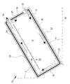
図1に反応器の形態をなす装置10のごく概要が示されている。その内室12に矢印14に沿って流れるガスが導かれる。反応器10は図示しない側壁のほかに底壁16、頂壁18、支壁20及びこれと平行又はほぼ平行に延びる縦側壁22によって画定される。支壁20が基板であって、その室内側がガス又はガス中にある元素と相互作用、例えば反応することも可能である。支壁20自体を基板として形成することもできる。当該の隔壁16、18、22が図示されている限り、反応器10の内室12は底面24、頂面26、基板面28及び縦境界面30によって画定される。
【0037】
頂壁18にガス入口又は進入口32とガス出口又は退出口34が設けられている。ここにおいて、入口32は縦側壁22の区域に、出口34は基板面28の区域にある。
【0038】
本発明によれば、基板面28が垂直線に対して、好ましくは、0°と、殆ど約90°の範囲内の角度αを描くように設定され、反応器10は垂直線又は水平に対して傾斜している。換言すれば、反応器10は水平に対する角度βが0°<β≦90°の関係にある。
【0039】
反応器10の種々の傾斜位置のごく概要が図2及び3で明らかである。
【0040】
入口32を経て好ましくは冷たいガスが反応室12に流入し、重力に基づき縦側面又は境界面30に沿って底面24に到達し、ここでガスが方向を転じ、次に基板面28へ導かれ、これに沿って流れる。ところがガス又はその元素がすでに基板面28と相互作用したガス部分、即ち被覆の場合は元素が基板面28にすでに析出されたガス部分だけが排出されるように、出口34は基板面28から間隔をおいて配設され、又は基板面28からある範囲まで伸張する。基板面28又は基板はガスの入口温度Tiより高い温度Tsに熱せれているから、縦境界面30及び底面24に沿って流れる間にガスの加熱が起こり、その結果ガスは対流に基づき基板面28に沿って流れ、層流が形成される。従って基板面28の被覆の場合は、基板面28に析出される元素に関して劣化したガス層38が基板面の近傍、即ち成層区域ないしゾーン40に形成される。この成層区域40は出口34を経て排出され、一方、成層区域40の外部に残るガス部分は、基板面8に析出し得る元素の濃度及び組成が入口32から流入するガスにほぼ相当する。
【0041】
特に図1および2に記載した矢印で明示するように、反応室12を貫流するガスは対流循環を形成し、その際基板面28に沿って層流が生じる。
【0042】
基板又は基板面28は流れるガスの上側に配置されているから、より大きな粒子が被覆される基板面28に到達することが防止される。基板の温度がその他の隔壁16、18、20の温度及び入口32から供給されるガスの温度に少なくとも等しく、特にそれより高いことから別の利点が生じる。その場合基板を反応ガスの上側に配置したことは、安定したガス流、即ち基板面28に沿った所望の層状の経過を保証する温度分布をもたらす。
【0043】
換言すれば、均質な析出率を得るために、対流の性質を被覆方法のために計画的に利用するのである。同じことが処理、例えば基板からの層の除去にも当てはまる。
【0044】
入口32から供給されるガスは冷たく、とりわけ重力に基づき縦境界壁30に沿って底部ヘ流れる。このために、縦側壁22及び反応器10は傾斜していなければならない。この場合、垂直線に対する傾斜角度αは0°ないし80°の範囲であり、ここにおける傾斜角度は0°をも含むものであり、又、水平に対する傾斜角度βは90°ないし10°の範囲であることが好ましい。
【0045】
縦境界面30に沿って流れる間にガスが徐々に加熱される。次に底面24に沿って方向転換が行われ、最後にガスは基板面28に沿って対流に基づき頂面26の方向へ上向きに流れる。こうしてガスは予め加熱された上で、基板面28に沿って導かれる。ガスは熱い基板に接して流れることにより、幅数センチメートルないし10センチメートルのゾーンの内部で加熱されるから、こうして対流循環の形成ための浮揚力と駆動力が与えられる。これに基づき基板面8に密接した熱ガスの通過流が生じる。その結果基板面28の近傍で化学反応が起こる。このことから被覆率と歩留に関して利点が生まれる。基板の傾斜は流れを促進し、傾斜角度の増大につれて速度が増加する。
【0046】
ガスが基板に沿ってますます熱くなり、それとともに流速がますます増加することにも触れておかねばならない。これによって劣化効果が補償される。
【0047】
前述のようにガス出口34は基板面28の直近に通っており、基板面28と平行なスロット状の幾何学形状が選定されている。こうして使用済みのガスは基板面28に沿って通過した直後に排出することができる。その場合出口34又は出口スロットの幅又は基板面28との間隔は、栄養成分に関して劣化したガスだけが排出されるように選定されている。そこで基板又は基板面28から大きな間隔で基板面に沿って流れ、従って未使用の熱せられたガスは頂面26に沿って入口32へ流れ、そこで新たに供給されたガスと混合される。これによって歩留が高められる。同時に基板面28に沿った濃度勾配が減少する。
【0048】
基板面28に沿って流れ、基板面28と相互作用する元素の拡散帯に相当する幅を有するガス層を排出することができるように、出口34のギャップ幅を選定しなければならない。
【0049】
このことを図1で基本的に明らかにする。成層区域40又は反応室12に通されたガスが栄養成分に関して劣化している層は、出口34から排出される。残りの部分は循環して流れ、こうして対流循環に従う。
【0050】
循環して流れる未使用のガスによって、反応室12の成層区域40又は拡散帯の前方に極めて均質な組成のガス混合物が生じる。こうして未使用の材料が絶えず補給される。このことは析出率の均質化をもたらす。同時に「反応速度低下」帯が発生しないように、少なくとも底面16又は基板面28の区域でガスを十分に加熱することが保証される。拡散層又は成層区域40に層流が得られることを保証する均一な温度分布を生じるために、場合によっては基板面28の区域でガスをさらに加熱しなければならない。
【0051】
基板44上にシリコン層を析出する本発明の第2の実施形態としての装置42が図3に示されている。ここにおいて、装置42は基本的に図1の装置に相当するから、同じ部材には同じ参照符号を使用する。
【0052】
図1の実施形態と異なり、図3では反応室12の密封のために石英ガラス板41、43の二重壁構造が設けられている。縦側壁22の石英ガラス板41と外側の石英ガラス壁48の間の間隙は通路45をなし、ここを不活性ガス例えばN2ガスが貫流することができる。間隙の掃気によって、反応室12の反応産物に原因する壁面付着物が石英ガラス板43から取り除かれる。さらに背面側では基板44に沿って冷却路46が通っており、ここでも例えばN2ガスが貫流することができる。冷却路46の外側は石英ガラス板43によって画定される。赤外線又は熱線が透過することができる石英ガラス壁48、50が縦側壁22又は基板40に沿って延びている。さらに石英ガラスからなる隔壁48、50に沿って例えば電灯の形の熱源52、54を配設することができる。底壁16と頂壁18は特殊鋼からなる。
【0053】
加熱装置52、54によって基板44を900℃ないし1600℃に加熱することができる。放射が石英ガラス壁48、50を通って反応室12に到達する。その場合窓とも呼ばれる石英ガラス壁48、50は、冷却路44、46を流れる冷ガスによって約900℃以下に冷却される。反応室12自体は石英ガラスで内張りされており、上側−図では左側−の面は基板面28からなる。このために基板44を反応室12の適当な保持具に配置することができる。その場合いわば通過法でシリコン層を基板上に被着するために、基板44を図平面の中へ又は図平面から外へ移動することができる。
【0054】
被覆のために水素(約20ないし2000slm)とトリクロルシラン(約1ないし200slm)の混合物のガスが大気圧で入口32から導入される。
【0055】
図3の原理図で明らかなように、入口32又は出口34の配置は見掛け上、図1の配置と異なる。即ち入口32及び出口34は頂壁18に沿って延びる偏向板56の下に配設されている。その場合偏向板56は、基板側又は縦境界面側でそれぞれギャップ58、60が生じる所まで、頂壁18に沿って延びている。ギャップ58、60は図1の寸法及び配列10の入口32又は出口34に相当する。こうして同じく基板面28に直接沿って流れ、栄養成分に関して劣化したガス分だけが反応室12から排出される。
【0056】
なお反応室12は大気に対して過圧を有することができることに触れておかねばならない。
【0057】
次に本発明を別の実施例で明らかにする。
【0058】
大型基板の上のSi層のCVD析出
好ましくは黒鉛又は場合によっては黒鉛含有セラミックスからなり、もしくは黒鉛を含む基板44をまず図3に従って反応室12に通す。その際温度約1000℃ないし1200℃に加熱される。トリクロルシランとH2からなる冷たい反応ガスがガス入口32及びギャップ60を通り、縦境界面30に沿って反応室12へ導かれる。縦境界面30と底面16に沿って流れる間にガスが加熱され、こうして浮揚させられることにより、反応室12の中に対流が起こり、その結果ガスが基板面28に沿って流れるから、基板44の上にシリコン層が析出される。
【0059】
本例では反応室12の高さHは約400mm、反応室12の幅は約200mmである。
【0060】
ガスは成層区域40に相当する狭いゾーンの中で反応によって消尽される。標準圧下で幅約1ないし2cmのこのゾーンは基板の頂部区域の出口ギャップ56から排出され、その際反応ガスゾーンの幅に合せてギャップ幅を設定することができる。基板44を傾けて配置したことにより、乱流及び未使用ガスと使用済みガスの混合が抑制され、不要の生成物は簡単に逃失することができる。
【0061】
ゾーン(成層区域40)の下側の区域には、偏向板56により縦境界壁30側へ転向される未使用ガスがある。同時に偏向板56に沿って冷却が起こり、さらに入口32又はギャップ60から反応室12へ導入される冷たい新気の混入によって、重力に基づき縦境界面30に沿ってガスの「落下」が起こる。続いて同様な循環が始まる。即ち反応室12の中に形成される対流循環によって未使用ガスが基板面28に沿って導かれ、基板面28の上に所望のシリコン層を形成する。
【0062】
ガスの不断の更新により成層区域40の前方の室内に極めて均質な濃度の区域が発生するから、全基板面28にわたって均質な析出率が保証される。なお実験が明らかにしたところでは、析出率は安定しており、広い範囲で傾斜角度βに左右されない。角度βは10°ないし90°の範囲にあることが好ましく、図4が明示するように特に60°≦β≦90°の範囲で、すこぶる均質となる。従ってこの角度範囲で安定な、即ち角度に比較的依存しない被覆率が得られる。
【0063】
そこで水平に対する傾斜角度βに関連して、析出率(毎分μm)と基板44の底部側縁端部からの間隔との関係を作図した。基板44として、底壁16と頂壁18の間隔に相当する400mmの長さの基板を利用した。底壁16からの僅かな間隔の後は析出率がほぼ一定であることが分かる。ただ傾斜角度βが0°のときだけは対流循環が発生しない。このため不安定が生じる。
【0064】
前述の例に従って被覆した基板44は、例えば長さ100mmの底部側縁端区域(CVD析出の始端)を除き、均質な被覆を有する。
【0065】
Si薄膜太陽電池のための半導体系のCVD析出
本発明に係る方法又は当該の装置によって、基本的に図5で明らかな結晶質シリコン薄膜太陽電池のための半導体積層システムないし積層系を製造することができる。積層システムは、好ましくは黒鉛又は黒鉛含有セラミックスからなり、もしくは黒鉛を含む基板62からなる。積層システムのベースは基板62、導電性SiC背面接点領域64又は代案と集積形配線の薄膜ソーラーモジュールの場合は電気絶縁性中間層、粗大結晶粒構造を有する高ドープシリコン結晶核層及びその上にエピタキシャル析出した感光性シリコン層68で構成される。当該の積層システムによって結晶シリコン技術で周知の種類の太陽電池を製造することができる。その場合MIS(金属−絶縁体半導体)逆転層太陽電池も、テスト構造としてpn接合を有する太陽電池も使用することができる。pn接合即ち拡散エミッタ70、金属正面グリル72及び反射防止層74の別の積層構造を有する太陽電池を図5に例示する。
【0066】
図5の積層システムを製造するために、本発明の学説により次の一連のプロセスが実施される。即ち
−基板の製造
−中間層(SiC又は窒化ケイ素もしくは両成分の金属混合物)のCVD析出
−p+−Si結晶核層のCVD析出
−SiOx保護層の被着
−p+−Si結晶核層の晶出
−SiOx保護層の除去
−光電池活性Si層のエピタキシャル成長(CVD)
−太陽電池構造(例えばMIS−IL法、pn法)
【0067】
詳細には、プロセスは次のように行われる。
a)中間層
一辺の長さ100mmないし1000mm、好ましくは300mmないし500mmで好ましくは黒鉛からなり、又は黒鉛を含み、又は黒鉛含有セラミックスからなる基板を基板温度約1300℃ないし1600℃に加熱する。その間にメチルトリクロルシランとH2からなる反応ガスの一部がガス入口32、60から反応室12に導入される。前述の機構に従って対流循環、及びそれに関連して拡散ゾーン(成層区域40)と循環する未使用ガスのゾーンが形成される。こうしてSiC層64が基板62の上に析出される。
【0068】
少量の窒素の添加によって導電性の窒素ドープSiC中間層を作ることができる。層厚は1μmないし100μm好ましくは30μmないし50μmである。
【0069】
基板を1200℃に加熱し、さらにクロルシランとNH3からなる反応ガスを大気圧下で40ないし100mbarの低圧で導入すれば、窒化ケイ素層が析出される。低圧で2つの物質の組合わせから、SiCと窒化ケイ素を含む層材料混合物を作ることができる。層(SiC、窒化ケイ素又は材料混合物)は電気絶縁性中間層及び汚染に対する防壁をなす。窒素ドープSiCで導電性中間層を作ることができる。層厚は1μmないし100μm、好ましくは30μないし50μmである。
【0070】
b)結晶核層
前記のSiC中間層64の上に、ホウ素を多量にドープしたSi層(p+−Si)を析出する。そのために上記の温度及びガス流量のパラメータを使用する。基板温度は約1000℃ないし1200℃、好ましくは1100℃でなければならない。反応ガスはトリクロルシラン及びH2からなり、BCl3が添加される。こうして作られた層は1μmないし100μm、好ましくは30μmないし50μmの厚さを有する。
【0071】
反応室12でCVD法で析出したp+−Si層を厚さ0.1μmないし5μm、好ましくは2μmの酸化ケイ素又は窒化ケイ素層で覆う。次に高ドープSi層を反応室の外で融解し、帯域溶融法(ZMR=zone melting and recrystalization)で横から晶出する。こうして数百μmないしcm領域の粒度が得られる。晶出層は結晶核層66をなす。保護層は、溶融物が収縮して滴になることを防止する。結晶化の後に酸化ケイ素又は窒化ケイ素層をエッチングして除く。これも同じく反応室12の中で実施することができる。
【0072】
c)光電池活性Si層
こうして作られ晶出した結晶核層66の上に約1・1016ないし1・1017cm− 3のホウ素をドープしたSi層68をエピタキシャル析出する。これも反応室12の中で行うことができる。Si層68は薄膜太陽電池のベースとしての光電池活性層をなす。エピタキシャル層68の厚さは2μmないし100μm、好ましくは15μmないし30μmである。15μm以下の厚さの場合は、高い効率を得るためにエピタキシャル層の背面で良好な光反射が必要である。
【0073】
d)太陽電池プロセス
太陽電池の製造のために、前述の積層システムないし積層系62、64、66、68の上に厚さ約0.1μmないし0.5μmの燐ドープSi層70を拡散させる。その上に正面グリル72又は透明な電極及びTiO2/MgF又はSiN等からなる厚さ約80nmの反射防止層74を被着する。こうして基本的に図5で明らかな薄膜太陽電池が成立する。絶縁性基板62が利用され、又は少なくとも層64が電気絶縁性に作られている限り、太陽電池を集積方式で配線することができる。
【図面の簡単な説明】
【図1】物体の面の処理又は被覆のための本発明の第1の実施形態の装置を示す概要図である。
【図2】図1に示す装置を垂直線に対して、(a)及び(b)で異なる角度状態を示す説明図である。
【図3】図1に対応する本発明の第2の実施形態の装置の概要図である。
【図4】面の上の析出率と面の傾斜角度との関係を表すグラフである。
【図5】c−Si薄膜太陽電池の層構成を示す図である。
【符号の説明】
12 室、反応室
24 底面
26 頂面
28 物体の面、基板の面
30 縦境界面
32 ガス入口
34 ガス出口
44 基板
52 熱源
54 熱源[0001]
BACKGROUND OF THE INVENTION
The present invention relates to a method for treating or coating a surface of an object, in particular a semiconductor component, for example a substrate surface of a solar cell as an object, by acting on the surface a gas containing small parts or particles that interact with the surface. The invention also includes a chamber defined by a top surface, a bottom surface, a side surface, a surface to be coated or treated and a longitudinal boundary surface parallel or substantially parallel thereto, a gas inlet and outlet, and at least one heat source for heating the surface. And an apparatus for coating or processing an object, for example, a surface of a substrate by applying a gas containing a small part or particles necessary for coating or processing.
[0002]
[Prior art and problems to be solved by the invention]
Various principles can be applied to coat a substrate or its surface as an object to be treated by CVD (chemical vapor deposition). For example, the gas flow can be guided parallel to the substrate surface. In that case the substrate is fixed or moved. By introducing the gas along the substrate surface, the carrier gas tends to deteriorate rapidly. Moreover, in the case of a fixed substrate, a non-uniform deposition rate, a non-uniform layer thickness, and a non-uniform doping in the direction of the layer thickness and layer surface are observed.
[0003]
When the substrate is moved, a uniform layer thickness can be obtained, but the deposition rate is inhomogeneous. In addition, non-uniform doping is observed in the direction of the layer thickness.
[0004]
In the overflow reactor, the gas sent to the substrate surface flows vertically from the top to the coating surface. In that case, if the substrate surface is small, a uniform deposition rate can be obtained. Concerning the layer thickness and doping in the layer thickness direction, homogeneity is also observed on the layer surface. However, when a large surface is coated, the return of the reacted gas is a problem, and the overflow reactor can achieve a good result only with a relatively small substrate surface.
[0005]
In order to obtain large surface homogeneous precipitation, a pancake reactor similar to the principle of an overflow reactor is utilized. This means that the flow is perpendicular to the surface to be coated. Since the substrate itself is placed on a hot susceptor, this provides sufficient mixing and homogenization of the gas by convection generated in the gas atmosphere. As a result, a uniform precipitation rate, a uniform layer thickness, and a homogeneous doping in the layer thickness and layer surface direction occur. Furthermore, the homogeneity can be improved by rotating the susceptor during coating. Even though such a coating method is suitable for large surface processing and yields a reproducible high quality epitaxial layer, gas is supplied from the center of the system through the hole in the disk-shaped susceptor and thus the wafer. It should be regarded as a drawback that it is limited to the application of coatings.
[0006]
The method described above and the reactor used are found in the literature, US Magazine: Chemical Vapor Deposition for Microelectron-cs, Arthur Sherman, Noycs Publici-ons, USA, pages 31-39, 150-174.
[0007]
It is known that inhomogeneities are averaged in the azimuthal direction by rotating the substrate to be coated in order to obtain good layer thickness uniformity. Therefore, in the CVD method in the semiconductor field, the substrate is rotated or at least moved. In that case, the rotation presupposes a rotationally symmetric substrate and a substrate support or susceptor with a precisely defined shape and an appropriate mass distribution.
[0008]
In the above techniques using horizontal CVD reactors, overflow reactors or pancake reactors, the substrate is usually on an inductive or lamp heated susceptor. If there is a gas on the substrate, often called a nutrient gas, that interacts with the substrate, the deposition of the layer and the quality of the layer is affected by the convection of the gas due to temperature rise. In that case, convection is highly turbulent and can be irregular. Moreover, when hot gas comes into contact with the incoming cold gas, condensation or nucleation occurs in the gas phase, which produces mist and dust. However, dusty deposits on the layer cause defects in the growing CVD layer. Particles also introduce defects that must be avoided in semiconductor and solar technologies.
[0009]
The object of the present invention is to improve the methods and devices of the kind mentioned at the outset so that sufficient planar or steric homogeneity is obtained with respect to the area of the surface to be treated or the coating applied to the surface. There is to do. Also, good efficiency when coating the surface, i.e. a sufficient coverage to gas flow ratio must be provided. In addition, a simple procedure must provide accurate gas guidance and flow.
[0010]
[Means for Solving the Problems and Effects of the Invention]
According to the present invention, this problem is determined in the method of the type mentioned at the outset by setting the surface of the object approximately at an angle α with respect to the vertical line, the angle α being in the
[0011]
In particular, in the present invention, the surface of the object is a boundary surface of a particularly rectangular parallelepiped chamber having a vertical boundary surface, a bottom surface, a top surface, and a side surface extending in parallel with the surface as boundaries, and the gas is on the top surface. It is introduced into the chamber in the zone and is guided along the longitudinal interface and the bottom surface and is then heated. The gas thus arriving into the chamber first flows along the longitudinal boundary surface due to gravity, then is guided along the bottom surface and is heated at least by the surface to be treated or coated, so that the gas flows along the surface by convection. Flowing. In that case, a part of the gas flowing directly along the surface of the object is discharged from the chamber, and the remaining part is circulated in the chamber. By this treatment, a small part interacting with the surface or part of the gas that has deteriorated with respect to the particles is discharged from a chamber, also called a reaction chamber. In that case, it is proposed that in particular the part of the gas discharged from the reaction chamber has a layer thickness of less than three times the thickness of the diffusion zone in which the gas particles interact with the surface of the object. Of the gas flowing in layers along the surface of the object, another portion of the particles that have not yet interacted with the surface can be circulated in the room to prevent random concentration changes. The exhausted spent gas is replenished with fresh cold gas. The cold gas is preferably replenished to the circulating gas via a slot. In order to ensure that the circulating partial gas stream “falls” along the longitudinal interface of the chamber which also extends parallel to or approximately parallel to the surface of the object, it is cooled with fresh, cold Mix with gas or cool vertical interface.
[0012]
The present invention avoids the disadvantages found in the prior art and provides significant advantages. This is because the used gas is discharged from the reaction chamber immediately after the reaction, the utilization of the unused gas is improved by gas circulation, and the deposition rate is uniform on the non-rotating substrate.
[0013]
Compared with the method in which the gas flow is guided horizontally to the non-rotating substrate surface, a more uniform deposition rate and a more uniform layer thickness and doping occur in the deposited layer. Compared to known methods of rotating the substrate, a more homogeneous doping of the deposited layer is provided. In addition, the manufacturing cost is low because it is not necessary to rotate the substrate. Compared to an overflow reactor, the advantage is that the deposition is more homogeneous in terms of deposition rate, layer thickness and doping on a large substrate surface.
[0014]
In the present invention, based on the use of convection circulation, the rectangular geometry of the reactor, and thus the rectangular substrate surface required for thin film technology, photovoltaic cells or for the manufacture of large TFT (thin film field transistor) screens is used. be able to.
[0015]
In the case of a pancake reactor, the hot substrate surface is on the lower side, so if small dust particles are deposited due to gravity and growth defects occur in the layer, the object is placed above the gas according to the present invention. By doing so, these defects can be eliminated.
[0016]
The surface of the object itself can be heated, for example by infrared radiation devices, microwaves, or inductively within a certain range, so that sufficient heat is supplied from the object to the gas flowing along the surface to form a convective circulation. Can be released.
[0017]
Further, by forming a convection circulation in the chamber, a low flow velocity band having a width substantially corresponding to the surface to be treated or coated is generated, which contributes to the uniformity of the treatment surface or the coating formed thereon.
[0018]
It is also possible to move the object parallel to the gas flowing in layers along the surface to be treated or coated so that the surface can be treated or coated by the passing method. An object with an area larger than the surface directly exposed to the gas is also possible.
[0019]
Further developing the present invention, the CH reacts with the surface to deposit a silicon carbide or silicon nitride containing layer on the object.ThreeSiClThreeAnd H2Or NHThreeOr SiH2Cl2, SiHClThree, SiClFourAnd H2Or NHThreeIt is also proposed to use a gas mixture of
[0020]
For the deposition of the silicon layer, SiHClThreeAnd H2A gas mixture of It is also possible to add a doping gas comprising, for example, diborane, boron trichloride, aluminum trichloride, gallium chloride or indium chloride to the gas mixture used.
[0021]
CuInGaSe on a glass substrate2In order to form a layer, H, deposited on the Cu, In, Ga layer deposited on the glass substrate2Se-containing gas is allowed to act.
[0022]
For the deposition of the tin oxide layer, the present invention applies tin tetrachloride and H on the glass substrate at a temperature of 400 ° C. to 550 ° C.2A gas mixture consisting of O vapor is applied. Due to the deposition of the silicon oxide layer, the present invention provides a silicon substrate or Si-coated substrate or p at temperatures from 400 ° C. to 600 ° C.+-SiCl core layer with SiClFourAnd H2A gas mixture consisting of O is allowed to act.
[0023]
Another proposal of the invention is that POCl is applied to the silicon layer.ThreeA phosphorus glass layer is formed by the action of a gas contained therein, and then the phosphorus glass layer thus obtained is heat-treated for phosphorus diffusion. As a result, a silicon layer in which phosphorus is homogeneously doped is obtained.
[0024]
However, not only the formation of the layer, but also the treatment of the surface and the removal of the layer from the surface are realized by the present invention. For example, the layer on the surface side of the object can be removed by the laminar flow of the HF-containing gas. The silicon oxide layer that occurs during the manufacture of the thin film solar cell and must be removed again can be removed uniformly, for example, by a laminar flow of HF-containing gas. HF or H that flows parallel to the layer and reacts with it2The silicon oxide layer can be uniformly removed by the O vapor-containing air. Finally, the silicon oxide layer in particular at the temperature TThree(TThree≧ 000 ° C) H2It was reduced by the laminar flow of the contained gas and thereby removed.
[0025]
The apparatus of the invention of the type mentioned at the outset for applying a gas containing a small part or particles necessary for coating or processing to an object, for example a substrate, to coat or treat the surface is treated or coated. The surface of the object is the boundary of the chamber and forms an angle α with respect to the vertical line, the angle α is in the
[0026]
The gas outlet itself extends parallel to the surface over the entire width or almost the entire width, thus forming a slot. In particular, the present invention assumes that the dimension of the gas outlet dimension has a slot width d (d ≦ 3D). Here, D is the width of the diffusion band of the gas element that interacts with the surface. In particular, the slot width d is configured to satisfy d≈D. That is, the size of the gas outlet is set to be three times or less of the width of the diffusion band, and particularly preferably approximately equal to or less than one time the width of the diffusion band.
[0027]
It is preferable to arrange the gas inlet in the area of the longitudinal boundary wall parallel or substantially parallel to the surface of the object and select a slot-like structure as well.
[0028]
It is preferable to align the surfaces of the object, ie the longitudinal boundary surface and preferably the top and bottom surfaces perpendicular to it, or to heat these surfaces so that the gas flowing in the chamber forms a convective circulation.
[0029]
Also, the surface of the object to be treated or coated is configured to specifically seal the opening of the chamber. Also, the chamber itself can have a slight overpressure to the outside world to eliminate gas ingress.
[0030]
In order to produce a semiconductor system using the apparatus according to the invention, the invention is characterized by the following process steps. That is
Deposition of SiC or silicon nitride-containing layer on a substrate made of, for example, silicon, ceramics or graphite, by CVD at room temperature T (900 ° ≦ T <2000 °, in particular 1200 ° ≦ T <1600 °),
A silicon layer doped with elements of group III of the periodic table (p+) Formation in the room,
Melting and crystallization of the doped silicon layer (possibly outdoors) and
Epitaxial growth of a polycrystalline silicon layer (p) and a photosensitive silicon layer (p layer) doped with a group III element and having a grain size of 0.1 to 10 mm.
[0031]
In addition, an n-doped layer, a conductive front contact, or an antireflection layer can be applied to a suitably manufactured laminated system or laminated system, and both the terminal layer and the antireflection layer can be formed indoors.
[0032]
P+Before crystallization of the layer, a silicon oxide layer having a thickness of 0.1 to 5 μm, preferably 1 to 2 μm is formed thereon, and then p+The layer can be melted and recrystallized in particular by zone melting. In this case, in order to expose a polycrystalline crystal nucleus layer having a grain size of 0.1 to 10 mm and to epitaxially deposit a p-layer thereon, the oxide layer is HF or H after crystallization.2Remove with contained gas.
[0033]
Other details, advantages and features of the present invention will become apparent in the preferred embodiments of the invention with reference to the following drawings in addition to the description of the claims and the above description.
[0034]
DETAILED DESCRIPTION OF THE INVENTION
For the purpose of coating or treating the surface of an object, in particular the surface of a substrate, embodiments of the invention will be described on the basis of the description of the figures seen in the drawings. Here, especially the CVD method is taken up for the deposition of silicon. However, the present invention is not limited to this. Instead of depositing the material, a chemical or physical change of the existing layer can also be made, for example as is done in connection with the drying process. Chemical transformations of existing layers can also be realized with the method of the invention.
[0035]
An important feature of the present invention is that a gas containing an element that interacts with a surface to be treated or coated is introduced into a chamber (hereinafter referred to as a reaction chamber), and a gas also called carrier gas or nutrient gas flows along the surface by convection. It can be seen that a laminar flow is formed.
[0036]
FIG. 1 shows a very schematic view of an
[0037]
The
[0038]
According to the present invention, the
[0039]
A very brief overview of the various tilted positions of the
[0040]
Preferably, cold gas flows into the
[0041]
In particular, as clearly shown by the arrows described in FIGS. 1 and 2, the gas flowing through the
[0042]
Since the substrate or
[0043]
In other words, in order to obtain a uniform precipitation rate, the nature of the convection is systematically used for the coating method. The same applies to processing, for example removal of layers from the substrate.
[0044]
The gas supplied from the
[0045]
The gas is gradually heated while flowing along the
[0046]
It should also be mentioned that the gas gets hotter along the substrate and the flow rate increases with it. This compensates for the degradation effect.
[0047]
As described above, the
[0048]
The gap width of the
[0049]
This is clarified basically in FIG. The layer in which the gas passed to the
[0050]
The circulated unused gas produces a highly homogeneous gas mixture in front of the
[0051]
An
[0052]
Unlike the embodiment of FIG. 1, in FIG. 3, a double wall structure of
[0053]
The
[0054]
For coating, a gas of a mixture of hydrogen (about 20 to 2000 slm) and trichlorosilane (about 1 to 200 slm) is introduced from the
[0055]
As apparent from the principle diagram of FIG. 3, the arrangement of the
[0056]
It should be noted that the
[0057]
Next, the present invention will be clarified by another embodiment.
[0058]
CVD deposition of Si layers on large substrates
A
[0059]
In this example, the height H of the
[0060]
The gas is exhausted by the reaction in a narrow zone corresponding to the
[0061]
In the lower zone of the zone (stratified zone 40), there is unused gas that is deflected by the deflecting
[0062]
Because of the constant renewal of the gas, a very homogeneous concentration zone is generated in the chamber in front of the
[0063]
Therefore, in relation to the inclination angle β with respect to the horizontal, the relationship between the deposition rate (μm per minute) and the interval from the bottom edge of the
[0064]
The
[0065]
Semiconductor-based CVD deposition for Si thin-film solar cells
With the method according to the invention or the device according to the invention, it is possible in principle to produce a semiconductor stacking system or stacking system for crystalline silicon thin-film solar cells which is evident in FIG. The laminated system is preferably made of graphite or graphite-containing ceramics, or of a
[0066]
In order to produce the stacked system of FIG. 5, the following series of processes is performed according to the theory of the present invention. That is
-Production of substrates
-CVD deposition of intermediate layer (SiC or silicon nitride or a metal mixture of both components)
-P+-CVD deposition of Si crystal nucleus layer
-SiOxProtective layer deposition
-P+-Crystallization of Si crystal nucleus layer
-SiOxRemoval of protective layer
-Epitaxial growth (CVD) of photovoltaic active Si layer
-Solar cell structure (eg MIS-IL method, pn method)
[0067]
Specifically, the process is performed as follows.
a) Middle layer
A substrate having a side length of 100 mm to 1000 mm, preferably 300 mm to 500 mm, preferably made of graphite, or containing graphite, or made of graphite-containing ceramics is heated to a substrate temperature of about 1300 ° C. to 1600 ° C. In the meantime, methyltrichlorosilane and H2A part of the reaction gas is introduced into the
[0068]
A conductive nitrogen-doped SiC interlayer can be made by adding a small amount of nitrogen. The layer thickness is 1 μm to 100 μm, preferably 30 μm to 50 μm.
[0069]
The substrate is heated to 1200 ° C., and chlorosilane and NHThreeWhen a reaction gas consisting of is introduced at a low pressure of 40 to 100 mbar under atmospheric pressure, a silicon nitride layer is deposited. A layer material mixture comprising SiC and silicon nitride can be made from a combination of two substances at low pressure. The layer (SiC, silicon nitride or material mixture) provides an electrically insulating interlayer and a barrier against contamination. A conductive intermediate layer can be made of nitrogen doped SiC. The layer thickness is 1 μm to 100 μm, preferably 30 μm to 50 μm.
[0070]
b) Crystal nucleus layer
On the SiC
[0071]
P deposited in the
[0072]
c) Photovoltaic cell active Si layer
About 1 · 10 on the
[0073]
d) Solar cell process
For the production of a solar cell, a phosphorous doped
[Brief description of the drawings]
FIG. 1 is a schematic diagram showing an apparatus of a first embodiment of the present invention for the treatment or coating of a surface of an object.
FIGS. 2A and 2B are explanatory views showing different angle states of the apparatus shown in FIG.
FIG. 3 is a schematic diagram of an apparatus according to a second embodiment of the present invention corresponding to FIG. 1;
FIG. 4 is a graph showing the relationship between the deposition rate on the surface and the inclination angle of the surface.
FIG. 5 is a diagram showing a layer configuration of a c-Si thin film solar cell.
[Explanation of symbols]
12 rooms, reaction chamber
24 Bottom
26 Top surface
28 Object surface, substrate surface
30 Longitudinal interface
32 Gas inlet
34 Gas outlet
44 substrates
52 heat source
54 Heat source
Claims (45)
Applications Claiming Priority (4)
| Application Number | Priority Date | Filing Date | Title |
|---|---|---|---|
| DE10117416.0 | 2001-04-06 | ||
| DE10117416 | 2001-04-06 | ||
| DE10143587A DE10143587A1 (en) | 2001-04-06 | 2001-09-05 | Method and device for treating and / or coating a surface of an object |
| DE10143587.8 | 2001-09-09 |
Publications (3)
| Publication Number | Publication Date |
|---|---|
| JP2002324761A JP2002324761A (en) | 2002-11-08 |
| JP2002324761A5 JP2002324761A5 (en) | 2005-09-15 |
| JP4249933B2 true JP4249933B2 (en) | 2009-04-08 |
Family
ID=26009032
Family Applications (1)
| Application Number | Title | Priority Date | Filing Date |
|---|---|---|---|
| JP2002103772A Expired - Fee Related JP4249933B2 (en) | 2001-04-06 | 2002-04-05 | Method and apparatus for the treatment or coating of object surfaces |
Country Status (4)
| Country | Link |
|---|---|
| US (1) | US6875468B2 (en) |
| EP (1) | EP1247587B1 (en) |
| JP (1) | JP4249933B2 (en) |
| DE (1) | DE50212201D1 (en) |
Families Citing this family (23)
| Publication number | Priority date | Publication date | Assignee | Title |
|---|---|---|---|---|
| EP1321446A1 (en) * | 2001-12-20 | 2003-06-25 | RWE Solar GmbH | Method of forming a layered structure on a substrate |
| DE102005058713B4 (en) * | 2005-12-08 | 2009-04-02 | Fraunhofer-Gesellschaft zur Förderung der angewandten Forschung e.V. | Method for cleaning the volume of substrates, substrate and use of the method |
| DE102006003464A1 (en) * | 2006-01-25 | 2007-07-26 | Degussa Gmbh | Formation of silicon layer on substrate surface by gas phase deposition, in process for solar cell manufacture, employs silicon tetrachloride as precursor |
| DE102006004702B3 (en) * | 2006-01-31 | 2007-10-25 | Cotec Gmbh | Method and device for all-over coating of objects |
| DE102006035644A1 (en) * | 2006-07-31 | 2008-02-14 | Advanced Micro Devices, Inc., Sunnyvale | A method of reducing contamination by providing a polymeric protective layer to be removed during processing of microstructures |
| NZ579354A (en) * | 2007-02-01 | 2011-03-31 | Willard & Kelsey Solar Group Llc | System and method for glass sheet semiconductor coating |
| US20100310860A1 (en) * | 2008-02-28 | 2010-12-09 | Changwon National University Industry Academy Cooperation Corps | Synthetic method for anti-oxidation ceramic coatings on graphite substrates |
| US20090250108A1 (en) * | 2008-04-02 | 2009-10-08 | Applied Materials, Inc. | Silicon carbide for crystalline silicon solar cell surface passivation |
| US20110018103A1 (en) * | 2008-10-02 | 2011-01-27 | Stion Corporation | System and method for transferring substrates in large scale processing of cigs and/or cis devices |
| IT1399480B1 (en) | 2010-03-15 | 2013-04-19 | Stral S R L | EQUIPMENT FOR DEPOSITION OF SEMICONDUCTIVE MATERIAL ON GLASS |
| KR20120097792A (en) * | 2011-02-25 | 2012-09-05 | 삼성전자주식회사 | Furnace and thin film forming method using the same |
| US9359261B2 (en) | 2013-05-07 | 2016-06-07 | Corning Incorporated | Low-color scratch-resistant articles with a multilayer optical film |
| US9110230B2 (en) | 2013-05-07 | 2015-08-18 | Corning Incorporated | Scratch-resistant articles with retained optical properties |
| US9366784B2 (en) | 2013-05-07 | 2016-06-14 | Corning Incorporated | Low-color scratch-resistant articles with a multilayer optical film |
| US9684097B2 (en) | 2013-05-07 | 2017-06-20 | Corning Incorporated | Scratch-resistant articles with retained optical properties |
| US9703011B2 (en) | 2013-05-07 | 2017-07-11 | Corning Incorporated | Scratch-resistant articles with a gradient layer |
| US10160688B2 (en) | 2013-09-13 | 2018-12-25 | Corning Incorporated | Fracture-resistant layered-substrates and articles including the same |
| US11267973B2 (en) | 2014-05-12 | 2022-03-08 | Corning Incorporated | Durable anti-reflective articles |
| US9335444B2 (en) | 2014-05-12 | 2016-05-10 | Corning Incorporated | Durable and scratch-resistant anti-reflective articles |
| US9790593B2 (en) | 2014-08-01 | 2017-10-17 | Corning Incorporated | Scratch-resistant materials and articles including the same |
| WO2017048700A1 (en) | 2015-09-14 | 2017-03-23 | Corning Incorporated | High light transmission and scratch-resistant anti-reflective articles |
| EP3837223A1 (en) | 2018-08-17 | 2021-06-23 | Corning Incorporated | Inorganic oxide articles with thin, durable anti-reflective structures |
| US11798808B1 (en) * | 2020-07-22 | 2023-10-24 | National Technology & Engineering Solutions Of Sandia, Llc | Method of chemical doping that uses CMOS-compatible processes |
Family Cites Families (7)
| Publication number | Priority date | Publication date | Assignee | Title |
|---|---|---|---|---|
| JPS5670830A (en) * | 1979-11-10 | 1981-06-13 | Toshiba Corp | Vapor growth method |
| US4468283A (en) * | 1982-12-17 | 1984-08-28 | Irfan Ahmed | Method for etching and controlled chemical vapor deposition |
| JPS6122621A (en) * | 1984-07-10 | 1986-01-31 | Sumitomo Electric Ind Ltd | Vapor-phase growing method |
| US4597986A (en) * | 1984-07-31 | 1986-07-01 | Hughes Aircraft Company | Method for photochemical vapor deposition |
| DE3772659D1 (en) * | 1986-06-28 | 1991-10-10 | Ulvac Corp | METHOD AND DEVICE FOR COATING USING A CVD COATING TECHNOLOGY. |
| JPH02178630A (en) * | 1988-12-29 | 1990-07-11 | Sharp Corp | Method and apparatus for forming thin polyimide film |
| US6265353B1 (en) * | 1996-06-05 | 2001-07-24 | Theva Duennschichttechnik Gmbh | Device and method for producing a multilayered material |
-
2002
- 2002-04-02 US US10/113,831 patent/US6875468B2/en not_active Expired - Fee Related
- 2002-04-05 JP JP2002103772A patent/JP4249933B2/en not_active Expired - Fee Related
- 2002-04-05 DE DE50212201T patent/DE50212201D1/en not_active Expired - Lifetime
- 2002-04-05 EP EP02007724A patent/EP1247587B1/en not_active Expired - Lifetime
Also Published As
| Publication number | Publication date |
|---|---|
| EP1247587B1 (en) | 2008-05-07 |
| JP2002324761A (en) | 2002-11-08 |
| EP1247587A2 (en) | 2002-10-09 |
| DE50212201D1 (en) | 2008-06-19 |
| EP1247587A3 (en) | 2003-12-03 |
| US20020160627A1 (en) | 2002-10-31 |
| US6875468B2 (en) | 2005-04-05 |
Similar Documents
| Publication | Publication Date | Title |
|---|---|---|
| JP4249933B2 (en) | Method and apparatus for the treatment or coating of object surfaces | |
| US4694779A (en) | Reactor apparatus for semiconductor wafer processing | |
| KR101938386B1 (en) | Apparatus for deposition of materials on a substrate | |
| CN100482857C (en) | Systems and methods for epitaxially depositing films on semiconductor substrates | |
| JP3008782B2 (en) | Vapor phase growth method and apparatus | |
| US9870937B2 (en) | High productivity deposition reactor comprising a gas flow chamber having a tapered gas flow space | |
| US4615298A (en) | Method of making non-crystalline semiconductor layer | |
| JP2002324761A5 (en) | ||
| US20080092812A1 (en) | Methods and Apparatuses for Depositing Uniform Layers | |
| US20030049372A1 (en) | High rate deposition at low pressures in a small batch reactor | |
| JPH08239295A (en) | Production of crystal and apparatus therefor | |
| JP2008072122A (en) | Wafer processing hardware for epitaxial deposition with which auto-doping and back surface defect are decreased | |
| CN1489644A (en) | Susceptorless reactor for growing epitaxial layers by chemical vapor deposition | |
| US20080193646A1 (en) | Vapor phase deposition apparatus and vapor phase deposition method | |
| US11149351B2 (en) | Apparatus and method for chemical vapor deposition process for semiconductor substrates | |
| JP2011001591A (en) | Gas heating apparatus | |
| US7118625B2 (en) | Liquid phase growth method for silicon crystal, manufacturing method for solar cell and liquid phase growth apparatus for silicon crystal | |
| TWI490367B (en) | Mocvd (metal organic chemical vapor deposition) method and apparatus thereof | |
| JP4443689B2 (en) | Film forming method and film forming apparatus | |
| JP2000243712A (en) | Film forming method and device | |
| CN111128696A (en) | Method for producing epitaxial silicon wafer and epitaxial silicon wafer | |
| JPS5952833A (en) | Plasma vapor reactor | |
| TWI828238B (en) | Heating devices, CVD equipment and semiconductor processing methods | |
| US20020012749A1 (en) | Method and apparatus for coating and/or treating substrates | |
| JPH0620038B2 (en) | Plasma gas phase reactor |
Legal Events
| Date | Code | Title | Description |
|---|---|---|---|
| A521 | Request for written amendment filed |
Free format text: JAPANESE INTERMEDIATE CODE: A523 Effective date: 20050405 |
|
| A621 | Written request for application examination |
Free format text: JAPANESE INTERMEDIATE CODE: A621 Effective date: 20050405 |
|
| A977 | Report on retrieval |
Free format text: JAPANESE INTERMEDIATE CODE: A971007 Effective date: 20080521 |
|
| A131 | Notification of reasons for refusal |
Free format text: JAPANESE INTERMEDIATE CODE: A131 Effective date: 20080527 |
|
| A601 | Written request for extension of time |
Free format text: JAPANESE INTERMEDIATE CODE: A601 Effective date: 20080826 |
|
| A602 | Written permission of extension of time |
Free format text: JAPANESE INTERMEDIATE CODE: A602 Effective date: 20080829 |
|
| A521 | Request for written amendment filed |
Free format text: JAPANESE INTERMEDIATE CODE: A523 Effective date: 20081127 |
|
| TRDD | Decision of grant or rejection written | ||
| A01 | Written decision to grant a patent or to grant a registration (utility model) |
Free format text: JAPANESE INTERMEDIATE CODE: A01 Effective date: 20081224 |
|
| A01 | Written decision to grant a patent or to grant a registration (utility model) |
Free format text: JAPANESE INTERMEDIATE CODE: A01 |
|
| A61 | First payment of annual fees (during grant procedure) |
Free format text: JAPANESE INTERMEDIATE CODE: A61 Effective date: 20090116 |
|
| FPAY | Renewal fee payment (event date is renewal date of database) |
Free format text: PAYMENT UNTIL: 20120123 Year of fee payment: 3 |
|
| R150 | Certificate of patent or registration of utility model |
Free format text: JAPANESE INTERMEDIATE CODE: R150 |
|
| FPAY | Renewal fee payment (event date is renewal date of database) |
Free format text: PAYMENT UNTIL: 20120123 Year of fee payment: 3 |
|
| FPAY | Renewal fee payment (event date is renewal date of database) |
Free format text: PAYMENT UNTIL: 20130123 Year of fee payment: 4 |
|
| FPAY | Renewal fee payment (event date is renewal date of database) |
Free format text: PAYMENT UNTIL: 20140123 Year of fee payment: 5 |
|
| R250 | Receipt of annual fees |
Free format text: JAPANESE INTERMEDIATE CODE: R250 |
|
| LAPS | Cancellation because of no payment of annual fees |