JP4238377B2 - Solid-state imaging device and driving method thereof - Google Patents
Solid-state imaging device and driving method thereof Download PDFInfo
- Publication number
- JP4238377B2 JP4238377B2 JP02286798A JP2286798A JP4238377B2 JP 4238377 B2 JP4238377 B2 JP 4238377B2 JP 02286798 A JP02286798 A JP 02286798A JP 2286798 A JP2286798 A JP 2286798A JP 4238377 B2 JP4238377 B2 JP 4238377B2
- Authority
- JP
- Japan
- Prior art keywords
- reset
- signal
- mos transistor
- photoelectric conversion
- switch
- Prior art date
- Legal status (The legal status is an assumption and is not a legal conclusion. Google has not performed a legal analysis and makes no representation as to the accuracy of the status listed.)
- Expired - Lifetime
Links
Images


Description
【0001】
【発明の属する技術分野】
本発明は、固体撮像素子およびその駆動方法に関し、特に単位画素ごとに増幅機能を持つMOS型イメージセンサなどの増幅型固体撮像素子およびその駆動方法に関する。
【0002】
【従来の技術】
従来、この種の増幅型固体撮像素子として、図13に示す構成の2次元固体撮像素子が知られている。すなわち、図13において、フォトダイオード101、増幅用MOSトランジスタ102、リセット用MOSトランジスタ103および垂直選択用MOSトランジスタ104によって単位画素105が構成され、リセット用MOSトランジスタ103のゲート電極が垂直リセット線108に、垂直選択用MOSトランジスタ104のゲート電極が垂直選択線109に、垂直選択用MOSトランジスタ104のソース電極が垂直信号線110にそれぞれ接続されている。
【0003】
また、垂直信号線110の一端と水平信号線111の間には、水平選択用MOSトランジスタ112が接続されている。そして、行選択をする垂直走査回路113から出力される2種類の垂直走査パルスφVSn,φVRnにより各行ごとに画素の動作が制御され、列選択をする水平走査回路114から出力される水平走査パルスφHmにより制御される水平選択用MOSトランジスタ112を介して画素信号が水平信号線111に出力される。その際、光電変換によってフォトダイオード101に蓄積された信号電荷が、増幅用MOSトランジスタ102によって信号電流に変換されて撮像素子の出力信号として導出される。
【0004】
【発明が解決しようとする課題】
しかしながら、上記構成の従来の増幅型2次元固体撮像素子では、各画素を構成する能動素子、主に増幅用MOSトランジスタ102の特性の画素ごとのバラツキ、特にMOSトランジスタのVth(閾値)バラツキがそのまま撮像素子の出力信号に乗ってきてしまう。この特性のバラツキは、画素ごとに固定の値を持つため、画面上に固定パターンノイズ(FPN;Fixed Patern Noise) として現れる。この固定パターンノイズを抑圧するためには、デバイスの外部にフレームメモリやラインメモリを用いたノイズ除去回路を設けて画素の特性のバラツキに起因するノイズ成分を除去する必要があり、したがって本固体撮像素子を撮像デバイスとして用いる例えばカメラシステムでは、ノイズ除去回路を外付けとする分だけ規模が大きくなってしまう。
【0005】
これに対し、固定パターンノイズをデバイスの内部で抑圧できるようにした増幅型固体撮像素子として、図14に示す構成のものが考えられる。この増幅型固体撮像素子においては、単位画素105の構成は図13と同じであるが、各画素105の特性のバラツキに起因する固定パターンノイズを抑圧するための水平出力回路115を設け、この水平出力回路115で画素105の読み出し前後(リセット前後)の信号の差分をとる処理を行うようにしている点が違う。
【0006】
図14において、垂直信号線110とグランドとの間には、増幅用MOSトランジスタ102のソースフォロワ動作の負荷として働く負荷用MOSトランジスタ116が接続されている。また、垂直信号線110には、一対の信号スイッチ用MOSトランジスタ117,117′の各一方の主電極が接続されている。この一対の信号スイッチ用MOSトランジスタ117,117′の各他方の主電極とグランドとの間には、一対の信号保持用キャパシタ118,118′がそれぞれ接続されている。
【0007】
また、一対の信号スイッチ用MOSトランジスタ117,117′の各他方の主電極と一対の水平信号線111,111′の間には、一対の水平選択用MOSトランジスタ112,112′がそれぞれ接続されている。一対の水平信号線111,111′には、差動アンプ119の非反転(+)入力端および反転(−)入力端がそれぞれ接続されている。
【0008】
上記構成の増幅型固体撮像素子においては、画素リセット前とリセット後のそれぞれの信号が、信号スイッチ用MOSトランジスタ117,117′を介して信号保持用キャパシタ118,118′に保持され、水平選択用MOSトランジスタ112,112′および水平信号線111,111′を介して差動アンプ119に供給される。そして、差動アンプ119において、画素リセット前とリセット後のそれぞれの信号の差分がとられることにより、単位画素ごとの特性のバラツキに起因する固定パターンノイズが除去される。
【0009】
しかしながら、上記構成の増幅型固体撮像素子では、単位画素ごとの特性のバラツキに起因する固定パターンノイズについては抑圧することはできるものの、画素リセット前とリセット後のそれぞれの信号が別々の信号経路を通って差動アンプ119に至ることから、一対の信号スイッチ用MOSトランジスタ117,117′や一対の水平選択用MOSトランジスタ112,112′の特性のバラツキが、垂直に相関を持つ縦筋状の固定パターンノイズとして画面上に現れることになる。したがって、この構成の場合にも、縦筋状の固定パターンノイズを抑圧するための補正回路がデバイスの外部に必要となる。
【0010】
本発明は、上記課題に鑑みてなされたものであり、その目的とするところは、単位画素ごとの特性のバラツキに起因する固定パターンノイズのみならず、縦筋状の固定パターンノイズをもデバイス内部で抑圧可能な増幅型固体撮像素子およびその駆動方法を提供することにある。
【0011】
【課題を解決するための手段】
本発明による固体撮像素子は、
入射光を光電変換しかつ光電変換によって得られた信号電荷を蓄積する光電変換素子と、
デプレッション型トランジスタで構成され、前記光電変換素子をリセットするリセットスイッチと、
前記光電変換素子に蓄積された信号電荷を電気信号に変換する増幅素子と、
前記増幅素子からの信号を選択的に出力する選択スイッチと、
デプレッション型MOSトランジスタからなり、リセットパルスに応答して前記リセットスイッチをオン/オフ制御するリセット選択スイッチと
を有し、前記リセットスイッチによるリセット前の信号とリセット後の信号とを共通の垂直信号線を経由して出力する単位画素と、
前記単位画素から出力されたリセット前の信号とリセット後の信号のそれぞれの差分をとる差分回路とを備え、
前記リセットスイッチは前記光電変換素子と電源線の間に接続され、
前記リセット選択スイッチは前記リセットスイッチのゲート電極と前記リセットパルスが与えられるリセット線の間に接続されている
構成となっている。
【0012】
また、本発明による駆動方法は、上記構成の固体撮像素子において、単位画素の各々で画素信号を出力するごとに光電変換素子をリセットスイッチによってリセットし、単位画素の各々からリセットスイッチによるリセット前の信号とリセット後の信号とを導出しかつ共通の伝送経路を経由して伝送し、しかる後リセット前の信号とリセット後の信号のそれぞれの差分をとるようにする。
【0013】
上記構成の固体撮像素子の単位画素の各々において、画素信号を出力するごとに光電変換素子をリセットすることで、各単位画素からはリセット前とリセット後の信号が1画素ごとに順次出力される。このとき、画素の特性のバラツキに起因する固定パターンノイズが、各画素の増幅素子からオフセット成分として発生することから、リセット前とリセット後の信号の差分をとることで、ノイズ成分をキャンセルできる。また、2次元固体撮像素子においては、リセット前とリセット後の信号を垂直信号線から水平信号線へ同一の信号経路を経由して出力することで、垂直に相関を持つ縦筋状のノイズ成分も原理的に発生しない。
【0014】
【発明の実施の形態】
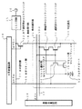
以下、本発明の実施の形態について図面を用いて詳細に説明する。図1は、2次元固体撮像素子に適用された本発明の第1実施形態を示す構成図である。
【0015】
図1において、破線で囲まれた領域が単位画素11を表している。この単位画素11は、光電変換素子であるフォトダイオード(PD)12と、増幅素子である増幅用MOSトランジスタ13と、選択スイッチである選択用MOSトランジスタ14と、リセットスイッチであるリセット用MOSトランジスタ15と、リセット選択用MOSトランジスタ16とから構成され、行列状に2次元配置されている。なお、図面上においては、簡略化のため、m列n行目の単位画素11のみを示している。
【0016】
この単位画素11において、フォトダイオード12は入射光を光電変換しかつ光電変換によって得られた信号電荷を蓄積する機能を持つ。このフォトダイオード12のカソード電極には、増幅用MOSトランジスタ13のゲート電極が接続されている。増幅用MOSトランジスタ13のドレイン電極は、電源(VDD)線17に接続されている。増幅用MOSトランジスタ13のソース電極と垂直信号線18の間には、選択用MOSトランジスタ14が接続されている。
【0017】
また、フォトダイオード12のカソード電極と電源線17の間には、リセット用MOSトランジスタ15が接続されている。リセット用MOSトランジスタ15のゲート電極と水平リセット線19の間には、リセット選択用MOSトランジスタ16が接続されている。リセット用MOSトランジスタ15およびリセット選択用MOSトランジスタ16としては、デプレッション型トランジスタが用いられている。このリセット選択用MOSトランジスタ16のゲート電極は、選択用MOSトランジスタ14のゲート電極と共に、垂直選択線20に接続されている。また、垂直信号線18と水平信号線21の間には、水平選択用MOSトランジスタ22が接続されている。
【0018】
また、行選択のための垂直走査回路23および列選択のための水平走査回路24が設けられている。そして、垂直走査回路23から出力される垂直走査パルスφVnが垂直選択線20に印加され、水平走査回路24から出力される水平リセットパルスφHRmが水平リセット線19に、水平走査パルスφHSm が水平選択用MOSトランジスタ22のゲート電極にそれぞれ印加される。すなわち、水平走査回路24が、水平リセットパルスφHRmを発生するリセット回路を兼ねることにより、回路構成の簡略化を図っている。
【0019】
水平信号線21の出力端側には、画素リセット前とリセット後のそれぞれの信号の差分をとる差分回路として、例えば回路構成が簡単な相関二重サンプリング回路(以下、CDS(Correlated Double Sampling)回路と称する)25が設けられている。このCDS回路25の具体的な回路構成およびその回路動作については、後で詳細に説明する。CDS回路25の出力端は、本撮像素子の出力端子26に接続されている。
【0020】
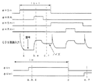
次に、上記構成の第1実施形態に係る増幅型固体撮像素子の動作について、図2のタイミングチャートを用いて説明する。
【0021】
先ず、光電変換によってフォトダイオード12に蓄積された信号電荷(電子)は、増幅用MOSトランジスタ13によって電気信号に変換される。そして、水平映像期間に入ると、垂直走査回路23から垂直走査パルスφVnが出力され、垂直選択線20を介して選択用MOSトランジスタ14およびリセット選択用MOSトランジスタ16の各ゲート電極に印加される。これにより、両MOSトランジスタ14,16が導通状態になり、選択用MOSトランジスタ14を通して信号電流が垂直信号線18に現れる。
【0022】
この水平映像期間中に、水平走査回路24から水平走査パルスφHSmが出力され、水平選択用MOSトランジスタ22のゲート電極に印加されることによって当該MOSトランジスタ22が導通状態になる。これにより、垂直信号線20に現れた信号電流は、水平選択用MOSトランジスタ22を通して水平信号線21に流れ、この水平信号線21を経てCDS回路25に供給される。
【0023】
その後すぐに、信号電流を出力したその同一画素に対し、水平走査回路24から水平リセットパルスφHRmが水平リセット線19に対して出力される。このとき、リセット選択用MOSトランジスタ16が導通状態にあることから、水平リセットパルスφHRmはこのリセット選択用MOSトランジスタ16を通してリセット用MOSトランジスタ15のゲート電極に印加される。これにより、リセット用MOSトランジスタ15が導通状態になるため、フォトダイオード12はVDDレベルにリセットされる。
【0024】
この水平リセットパルスφHRmは、図2のタイミングチャートから明らかなように、水平走査パルスφHSmの発生期間のほぼ中間で発生される。したがって、水平リセットパルスφHRmの消滅後、即ちリセット後のフォトダイオード12の電荷(ノイズ成分)が増幅用MOSトランジスタ13で電流に変換され、そのリセット電流が導通状態にある選択用MOSトランジスタ14、垂直信号線18および導通状態にある水平選択用MOSトランジスタ22を通して水平信号線21に流れ、この水平信号線21を経てCDS回路25に供給される。
【0025】
以上の一連の動作により、1つの画素11について信号出力→PDリセット→ノイズ出力という形で信号出力とリセット出力が順次得られる。これを垂直走査回路23で選択された画素行に対して、水平走査回路24によって順次画素選択を行うことにより、m列n行(信号出力→PDリセット→ノイズ出力)、m+1列n行(信号出力→PDリセット→ノイズ出力)、……という順番で水平信号線21に出力され、CDS回路25に供給される。そして、このCDS回路25において、リセット前の信号出力とリセット後のノイズ出力を使って相関二重サンプリングを行うことにより、主に増幅用MOSトランジスタ13の特性のバラツキ成分を除去することができる。
【0026】
図3に、CDS回路25の具体的な回路構成の一例を示す。このCDS回路25は、入力端子31に入力端が接続された電流電圧変換回路32と、この電流電圧変換回路32の出力端に一端が接続されたクランプキャパシタ33と、このクランプキャパシタ33の他端に一方の主電極が接続されたクランプMOSトランジスタ34と、クランプキャパシタ33の他端に一方の主電極が接続されたサンプルホールドMOSトランジスタ35と、このサンプルホールドMOSトランジスタ35の他方の主電極とグランドとの間に接続されたサンプルホールドキャパシタ36と、サンプルホールドMOSトランジスタ35の他方の主電極と出力端子38との間に接続されたバッファアンプ37とから構成されている。
【0027】
このCDS回路25において、電流電圧変換回路32は、入力端子31を介して供給される信号電流を反転(−)入力とし、所定のバイアス電圧Vbを非反転(+)入力とする差動アンプ39と、この差動アンプ39の反転入力端と出力端間に接続された帰還抵抗40とからなり、信号電流を信号電圧に変換する。クランプMOSトランジスタ34の他方の主電極にはクランプ電圧Vclが、そのゲート電極にはクランプパルスφCLがそれぞれ印加される。また、サンプルホールドMOSトランジスタ35のゲート電極には、サンプルホールドパルスφSHが印加される。
【0028】
上記構成のCDS回路25を差分回路として用い、リセット前の信号出力とリセット後のノイズ出力を使って相関二重サンプリングを行うことにより、増幅用MOSトランジスタ13の特性の画素ごとのバラツキ、特にMOSトランジスタのVthバラツキを除去することができる。
【0029】
上述したように、各単位画素11のフォトダイオード12のリセットを、1画素の信号が出力されるごとに行うようにするとともに、リセット前の信号出力とリセット後のノイズ出力を使って相関二重サンプリングを行うようにしたことにより、画素の特性のバラツキに起因する固定パターンノイズおよび垂直信号線18に接続されたスイッチ素子(水平選択用MOSトランジスタ22)の特性のバラツキに起因する縦筋状の固定パターンノイズを抑圧できる。
【0030】
すなわち、画素の特性のバラツキに起因する固定パターンノイズについては、単位画素11の増幅用MOSトランジスタ13からオフセット成分として発生するが、原理的に、画素リセット前とリセット後の信号を相関二重サンプリングすることによって除去できる。また、垂直信号線18に接続されたスイッチ素子の特性のバラツキに起因する縦筋状の固定パターンノイズについては、画素リセット前とリセット後の信号が同一の信号経路を通る構成となっており、別々のスイッチ素子(水平選択用MOSトランジスタなど)を通ることがないため、これも原理的に発生することがない。
【0031】
ここで、フォトダイオード12のリセット動作についてさらに詳しく述べる。なお、図1から明らかなように、リセット用MOSトランジスタ15およびリセット選択用MOSトランジスタ16として、デプレッション型トランジスタが用いられている。
【0032】
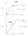
フォトダイオード12をVDDレベルにリセットする際に、リセット選択用MOSトランジスタ16にエンハンスメント型トランジスタを使った場合には、垂直走査パルスφVnによって選択された状態において、水平リセットパルスφHRmがリセット選択用MOSトランジスタ16のドレイン電極に印加されても、図4(A)に示すように、飽和領域の動作となるために、ソース側の電位はドレイン側の電位よりも落ちてしまうことになる。
【0033】
これに対し、リセット選択用MOSトランジスタ16としてデプレッション型トランジスタを使うことにより、図4(B)に示すように、線型領域での動作となり、ソース側の電位がほぼドレイン側の電位まで達する。同様に、リセット用MOSトランジスタ15にもエンハンスメント型トランジスタを用いると、飽和領域でのリセット動作となり、リセットの時間が短いと電荷の取り残しが生じ、残像の原因となる。これに対し、デプレッション型トランジスタを用いて線型領域でリセットすることにより、電荷の取り残しの無い、完全なリセット動作が可能となる。
【0034】
次に、上記構成の第1実施形態に係る増幅型固体撮像素子の動作について、図2のタイミングチャートに基づいて図5のポテンシャル図を用いて説明する。
【0035】
選択画素の信号読み出し時(図2のタイミングa)には、垂直走査パルスφVnによってリセット選択用MOSトランジスタ16が導通状態となり、ソース側の電位である水平リセットパルスφHRmの“L”レベルの電位がリセット用MOSトランジスタ15のゲート電極に印加される。このとき、リセット用MOSトランジスタ15は導通状態にならないので、フォトダイオード12に蓄積された信号電荷が増幅用MOSトランジスタ13で信号電流に変換される。
【0036】
選択画素のリセット時(図2のタイミングb)には、“H”レベルの水平リセットパルスφHRmが導通状態のリセット選択用MOSトランジスタ16を経てリセット用MOSトランジスタ15のゲート電極に印加され、これによりリセット用MOSトランジスタ15が導通状態となるため、フォトダイオード12がVDDレベルにリニア領域で完全リセットされる。
【0037】
選択画素のノイズレベル読み出し時(図2のタイミングc)には、水平リセットパルスφHRmが“L”レベルの状態にあり、この“L”レベルが導通状態のリセット選択用MOSトランジスタ16を経てリセット用MOSトランジスタ15のゲート電極に印加されることによってリセット用MOSトランジスタ15が非導通状態になる。これにより、リセットのレベルが増幅用MOSトランジスタ13でノイズ電流に変換される。また、この時点より次のフレーム蓄積が開始される。
【0038】
信号電荷の蓄積時(図2のタイミングd)、即ち他の行の他の列の読み出し時には、垂直走査パルスφVmが“L”レベルに遷移するが、リセット選択用MOSトランジスタ16がデプレッション型であるために、リセット用MOSトランジスタ15のゲート電極はフローティング状態にはならず、“L”レベルに保たれる。
【0039】
非選択画素のリセット時(図2のタイミングe)には、“H”レベルの水平リセットパルスφHRmによりリセット選択用MOSトランジスタ16のドレインがVDDレベルになると、リセット選択用MOSトランジスタ16のゲート電極の“L”レベルのポテンシャルに応じた電位が、リセット用MOSトランジスタ15のゲート電極に印加される。なお、フォトダイオード12は、デプレッションのリセットゲートがそのまま横型オーバーフローバリアになっていて、このレベルを超える電荷は電源へと捨てられるようになっているが、この時点でオーバーフローバリアが下がり、ここでオーバーフローレベルが決まる。
【0040】
ところで、単位画素の構成を考えた場合に、図6又は図7に示すように、リセット用MOSトランジスタ15とリセット選択用MOSトランジスタ16を、フォトダイオード12のカソード電極と電源線17の間に直列に接続し、リセット用MOSトランジスタ15のゲート電極に水平リセットパルスφHRm又は垂直走査パルスφVnを、リセット選択用MOSトランジスタ16のゲート電極に垂直走査パルスφVn又は水平リセットパルスφHRmを印加する構成が一般的に考えられる。
【0041】
しかしながら、これらの構成の場合には、リセット用MOSトランジスタ15とリセット選択用MOSトランジスタ16によるフィードスルーが、信号レベルを読み出す際とノイズレベルを読み出す際で異なってしまい、これが画素ごとのバラツキの原因となる。その理由について、図6の構成に対応した図8のポテンシャル図を用いて以下に説明する。
【0042】
先ず、垂直走査パルスφVnの発生によって画素が選択され、水平リセットパルスφHRmの発生によってリセットされているときを状態1.とする。この状態1.では、フォトダイオード12はVDDレベルにリセットされている。そして、状態2.では、水平リセットパルスφHRmが消滅し、リセット用MOSトランジスタ15がオフする際のフィードスルーの影響で、フォトダイオード12のポテンシャルはVDDレベルよりも僅かに浅くなる。この状態でノイズレベルの読み出しとなる。
【0043】
状態3.では、垂直走査パルスφVnが消滅することで非選択状態となる。リセット選択用MOSトランジスタ16がオフする際のフィードスルーの影響で、リセット用MOSトランジスタ15とリセット選択用MOSトランジスタ16の間の拡散領域のポテンシャルはVDDレベルよりも僅かに浅くなる。
【0044】
状態4.は電荷の蓄積状態であり、フォトダイオード12のポテンシャルが蓄積された電荷により浅くなっていく。状態5.は、非選択のリセット状態、即ち他の行の同じ列がリセットされている状態であり、水平リセットパルスφHRmの発生により、リセット用MOSトランジスタ15が導通状態となり、信号電荷とリセットゲートのフィードスルーおよびリセット選択ゲートのフィードスルーが合わされる。
【0045】
状態6.で水平リセットパルスφHRmが消滅するときに、さらにフォトダイオード12にリセットゲートのフィードスルーが加わる。他の行を読み出している期間中、状態5.状態6.を繰り返す。状態7.で、垂直走査パルスφVnの発生により、リセット選択用MOSトランジスタ16が導通状態となり、この状態で信号レベルが読み出される。この後、状態1.に戻る。
【0046】
図8のポテンシャル図において、状態2.と状態7.の比較から明らかなように、状態7.の信号レベルの読み出し時と、状態2.のノイズレベルの読み出し時では、フォトダイオード12に蓄えられているフィードスルーによる電荷の量が異なる。フィードスルーの量は、Vthバラツキと同様に個々のトランジスタによって異なるので、信号レベルの読み出しとノイズレベルの読み出しのフィードスルーの違いは、画素バラツキを抑圧するためのCDS回路25ではキャンセルすることができず、そのまま画素バラツキとして残ってしまう。
【0047】
リセット用MOSトランジスタ15とリセット選択用MOSトランジスタ16の接続関係を逆にした図7の構成の場合にも、図9のポテンシャル図から明らかなように、図6の構成の場合と同様のことが言える。
【0048】
これに対し、本実施形態においては、リセット用MOSトランジスタ15のゲート電極に、リセット選択用MOSトランジスタ16のソース電極を接続し、リセット選択用MOSトランジスタ16のドレイン電極、ソース電極を介してリセット用MOSトランジスタ15のゲート電極に水平リセットパルスφHRmを印加する構成としたことで、ノイズ読み出し時、信号読み出し時のいずれにおいても、リセット選択ゲートによるフィードスルーの影響がないので、各画素ごとのリセットゲートによるフィードスルーのバラツキは後段のCDS回路25で抑圧することができる。
【0049】
図10は、1次元固体撮像素子に適用された本発明の第2実施形態を示す構成図である。
【0050】
図10において、破線で囲まれた領域が単位画素51を表している。この単位画素51は、光電変換素子であるフォトダイオード(PD)52と、増幅素子である増幅用MOSトランジスタ53と、選択スイッチである選択用MOSトランジスタ54と、リセットスイッチであるリセット用MOSトランジスタ55とから構成され、直線状に1次元配置されている。
【0051】
この単位画素51において、フォトダイオード52は入射光を光電変換しかつ光電変換によって得られた信号電荷を蓄積する機能を持つ。このフォトダイオード52のカソード電極には、増幅用MOSトランジスタ53のゲート電極が接続されている。増幅用MOSトランジスタ53のドレイン電極は、電源(VDD)線56に接続されている。
【0052】
増幅用MOSトランジスタ53のソース電極と信号線57の間には、選択用MOSトランジスタ54が接続されている。また、フォトダイオード52のカソード電極と電源線56の間には、リセット用MOSトランジスタ55が接続されている。このリセット用MOSトランジスタ55としては、デプレッション型トランジスタが用いられている。
【0053】
また、1次元配列された単位画素51を順に選択するための走査回路58が設けられている。そして、この走査回路58から出力される走査パルスφHSmが選択用MOSトランジスタ54のゲート電極に、リセットパルスφHRmがリセット用MOSトランジスタ55のゲート電極にそれぞれそれぞれ印加される。すなわち、走査回路58が、リセットパルスφHRmを発生するリセット回路を兼ねることにより、回路構成の簡略化を図っている。
【0054】
信号線57の出力端側には、画素リセット前とリセット後のそれぞれの信号の差分をとる差分回路として、例えば回路構成が簡単なCDS回路59が設けられている。このCDS回路59としては、先の実施形態の場合と同様に、図3に示す回路構成のものが用いられる。
【0055】
次に、上記構成の第2実施形態に係る増幅型固体撮像素子の動作について、図11のタイミングチャートを用いて説明する。
【0056】
先ず、光電変換によってフォトダイオード52に蓄積された信号電荷(電子)は、増幅用MOSトランジスタ53によって電荷信号に変換される。そして、走査回路58から走査パルスφHSmが出力されると、選択用MOSトランジスタ54が導通状態になり、この選択用MOSトランジスタ54を通して信号電流が信号線57を経てCDS回路59に供給される。
【0057】
その後すぐに、信号電流を出力した同一画素に対し、走査回路58からリセットパルスφHRmが出力され、リセット用MOSトランジスタ55のゲート電極に印加される。これにより、リセット用MOSトランジスタ55が導通状態となるため、フォトダイオード52はVDDレベルにリセットされる。
【0058】
このリセットパルスφHRmは、図11のタイミングチャートから明らかなように、走査パルスφHSmの発生期間(“H”レベルの期間)内で発生される。したがって、リセットパルスφHRmの消滅後、即ちリセット後のフォトダイオード52の電荷(ノイズ成分)が増幅用MOSトランジスタ53で電流に変換され、そのリセット電流が導通状態にある選択用MOSトランジスタ54を通して信号線57に流れ、この信号線57を経てCDS回路59に供給される。
【0059】
以上の一連の動作により、1つの画素51について信号出力→PDリセット→ノイズ出力という形で信号出力とリセット出力が順次得られ、CDS回路59に供給される。そして、CDS回路59において、リセット前の信号出力とリセット後のノイズ出力を使って相関二重サンプリングを行うことにより、主に増幅用MOSトランジスタ53の特性のバラツキ成分を抑圧することができる。
【0060】
ここで、フォトダイオード52のリセット動作についてさらに詳しく述べる。なお、図10から明らかなように、リセット用MOSトランジスタ55として、デプレッション型トランジスタが用いられている。
【0061】
フォトダイオード52をVDDレベルにリセットする際に、リセット用MOSトランジスタ55にエンハンスメント型トランジスタを使った場合には、リセットパルスφHRmによって選択された状態でリセット用MOSトランジスタ55のドレイン電極に電源VDDが印加されても、図4(A)に示すように、飽和領域の動作となるため、ソース側の電位はドレイン側の電位よりも落ちてしまい、リセットの時間が短いと電荷の取り残しが生じ、残像の原因となる。
【0062】
これに対して、リセット用MOSトランジスタ55としてデプレッション型トランジスタを使うことにより、図4(B)に示すように、線型領域での動作となり、ソース側の電位がほぼドレイン側の電位まで達するため、電荷の取り残しの無い、完全なリセット動作が可能となる。
【0063】
続いて、上記構成の第2実施形態に係る増幅型固体撮像素子の動作について、図11のタイミングチャートに基づいて図12のポテンシャル図を用いて説明する。
【0064】
信号読み出し時(図11のタイミングa)には、リセット用MOSトランジスタ55は導通状態にはならないので、フォトダイオード52に蓄積された信号電荷が増幅用MOSトランジスタ53で信号電流に変換される。
【0065】
リセット時(図11のタイミングb)には、“H”レベルのリセットパルスφHRmがリセット用MOSトランジスタ55のゲート電極に印加され、これによりリセット用MOSトランジスタ55が導通状態となるため、フォトダイオード52がVDDレベルにリニア領域で完全リセットされる。
【0066】
ノイズレベル読み出し時(図11のタイミングc)には、リセットパルスφHRmが“L”レベルの状態にあり、リセット用MOSトランジスタ55が非導通状態になる。これにより、リセットのレベルが増幅用MOSトランジスタ53でノイズ電流に変換される。また、この時点(図11のタイミングd)より次のフレーム蓄積が開始される。
【0067】
なお、フォトダイオード52は、デプレッションのリセットゲートがそのまま横型オーバーフローバリアになっていて、このレベルを超える電荷は電源へと捨てられるようになっている。オーバーフローレベルは、リセット用MOSトランジスタ55のゲート電位の“L”レベルのポテンシャルである。
【0068】
【発明の効果】
以上説明したように、本発明によれば、単位画素ごとに増幅機能を持つ固体撮像素子において、単位画素の各々で画素信号を出力するごとに光電変換素子を完全リセットする構成としたことにより、各画素より信号成分とノイズ成分を順次出力することができるので、リセット前後の差分をとることによって固定パターンノイズを抑圧することができる。また、各画素を完全リセットしているので残像の発生もなく、さらに2次元固体撮像素子においては、信号成分とノイズ成分が垂直信号線から水平信号線へ同一の経路を経由して出力されるので、縦筋状の固定パターンノイズの発生も抑えることができる。
【図面の簡単な説明】
【図1】本発明の第1実施形態を示す構成図である。
【図2】第1実施形態の動作説明のためのタイミングチャートである。
【図3】CDS回路の回路構成の一例を示す回路図である。
【図4】エンハンスメント型MOSトランジスタ(A)とデプレッション型MOSトランジスタ(B)のId−Vd特性図である。
【図5】第1実施形態に係るリセット部の動作説明のためのポテンシャル図である。
【図6】単位画素の他の構成例を示す回路図である。
【図7】単位画素のさらに他の構成例を示す回路図である。
【図8】図5の構成に対応したポテンシャル図である。
【図9】図6の構成に対応したポテンシャル図である。
【図10】本発明の第2実施形態を示す構成図である。
【図11】第2実施形態の動作説明のためのタイミングチャートである。
【図12】第2実施形態に係るリセット部の動作説明のためのポテンシャル図である。
【図13】従来例を示す構成図である。
【図14】課題を説明するための構成図である。
【符号の説明】
11,51…単位画素、12,52…フォトダイオード(光電変換素子)、13,53…増幅用MOSトランジスタ、14,54…選択用MOSトランジスタ、15,55…リセット用MOSトランジスタ、16…リセット選択用MOSトランジスタ、17,56…電源(VDD)線、18…垂直信号線、19…水平リセット線、20…垂直選択線、21…水平信号線、22…水平選択用MOSトランジスタ、23…垂直走査回路、24…水平走査回路、25,59…CDS(相関二重サンプリング)回路、57…信号線、58…走査回路[0001]
BACKGROUND OF THE INVENTION
The present invention relates to a solid-state imaging device and a driving method thereof, and more particularly to an amplifying solid-state imaging device such as a MOS image sensor having an amplification function for each unit pixel and a driving method thereof.
[0002]
[Prior art]
Conventionally, a two-dimensional solid-state image sensor having the configuration shown in FIG. 13 is known as this type of amplification type solid-state image sensor. That is, in FIG. 13, a unit pixel 105 is constituted by the photodiode 101, the amplification MOS transistor 102, the reset MOS transistor 103, and the vertical
[0003]
A horizontal
[0004]
[Problems to be solved by the invention]
However, in the conventional amplification type two-dimensional solid-state imaging device having the above-described configuration, the variation of the characteristics of the active element constituting each pixel, mainly the characteristics of the amplification MOS transistor 102, particularly the Vth (threshold) variation of the MOS transistor remains unchanged. It gets on the output signal of the image sensor. This variation in characteristics has a fixed value for each pixel, and thus appears as fixed pattern noise (FPN) on the screen. In order to suppress this fixed pattern noise, it is necessary to provide a noise removal circuit using a frame memory or line memory outside the device to remove noise components caused by variations in pixel characteristics. For example, in a camera system that uses an element as an imaging device, the scale is increased by the amount of an external noise removal circuit.
[0005]
On the other hand, a configuration shown in FIG. 14 is conceivable as an amplifying solid-state imaging device capable of suppressing fixed pattern noise inside the device. In this amplification type solid-state imaging device, the configuration of the unit pixel 105 is the same as that in FIG. 13, but a horizontal output circuit 115 is provided for suppressing fixed pattern noise caused by variations in characteristics of each pixel 105. The difference is that the output circuit 115 performs a process of calculating a difference between signals before and after the pixel 105 is read (before and after reset).
[0006]
In FIG. 14, a
[0007]
A pair of horizontal
[0008]
In the amplification type solid-state imaging device having the above-described configuration, the respective signals before and after the pixel reset are held in the signal holding capacitors 118 and 118 'via the signal switch MOS transistors 117 and 117', for horizontal selection. The signal is supplied to the differential amplifier 119 via the
[0009]
However, in the amplification type solid-state imaging device having the above configuration, although it is possible to suppress the fixed pattern noise caused by the characteristic variation for each unit pixel, the respective signals before and after the pixel reset have different signal paths. Through the differential amplifier 119, the variation in characteristics of the pair of signal switch MOS transistors 117 and 117 'and the pair of horizontal
[0010]
The present invention has been made in view of the above-described problems, and the object of the present invention is not only fixed pattern noise caused by variation in characteristics of each unit pixel but also vertical streak-like fixed pattern noise. It is an object of the present invention to provide an amplifying solid-state imaging device that can be suppressed and a driving method thereof.
[0011]
[Means for Solving the Problems]
The solid-state imaging device according to the present invention is
A photoelectric conversion element that photoelectrically converts incident light and accumulates signal charges obtained by photoelectric conversion;
A reset switch configured by a depletion type transistor to reset the photoelectric conversion element;
An amplifying element that converts the signal charge accumulated in the photoelectric conversion element into an electrical signal;
A selection switch for selectively outputting a signal from the amplification element;,
A reset selection switch comprising a depletion type MOS transistor, which controls on / off of the reset switch in response to a reset pulse;
A signal before resetting by the reset switch and a signal after resetting.verticalA unit pixel that is output via a signal line;
A difference circuit for calculating a difference between a signal before reset and a signal after reset output from the unit pixel;,
The reset switch is connected between the photoelectric conversion element and a power line,
The reset selection switch is connected between a gate electrode of the reset switch and a reset line to which the reset pulse is applied.
It has a configuration.
[0012]
Further, the driving method according to the present invention is a solid-state imaging device having the above-described configuration, in which a photoelectric conversion element is provided each time a pixel signal is output from each unit pixel.By reset switchReset from each of the unit pixelsBy reset switchDerivation of the signal before resetting and the signal after resetting and common transmissionRouteAfter that, the difference between the signal before resetting and the signal after resetting is taken.
[0013]
In each of the unit pixels of the solid-state imaging device having the above-described configuration, the photoelectric conversion element is reset every time a pixel signal is output, so that signals before and after reset are sequentially output from each unit pixel for each pixel. . At this time, fixed pattern noise resulting from variations in pixel characteristics is generated as an offset component from the amplifying element of each pixel. Therefore, the noise component can be canceled by taking the difference between the signals before and after the reset. In a two-dimensional solid-state image sensor, vertical streak-like noise components that are vertically correlated by outputting pre-reset and post-reset signals from the vertical signal line to the horizontal signal line via the same signal path. Does not occur in principle.
[0014]
DETAILED DESCRIPTION OF THE INVENTION
Hereinafter, embodiments of the present invention will be described in detail with reference to the drawings. FIG. 1 is a configuration diagram showing a first embodiment of the present invention applied to a two-dimensional solid-state imaging device.
[0015]
In FIG. 1, a region surrounded by a broken line represents a
[0016]
In the
[0017]
A
[0018]
Further, a vertical scanning circuit 23 for selecting a row and a
[0019]
On the output end side of the horizontal signal line 21, a differential double sampling circuit (hereinafter referred to as a CDS (Correlated Double Sampling) circuit having a simple circuit configuration, for example) is used as a differential circuit that takes a difference between signals before and after pixel reset. 25) is provided. The specific circuit configuration and circuit operation of the
[0020]
Next, the operation of the amplification type solid-state imaging device according to the first embodiment having the above configuration will be described with reference to the timing chart of FIG.
[0021]
First, signal charges (electrons) accumulated in the photodiode 12 by photoelectric conversion are converted into electric signals by the
[0022]
During this horizontal video period, a horizontal scanning pulse φHSm is output from the
[0023]
Immediately thereafter, a horizontal reset pulse φHRm is output from the
[0024]
As is apparent from the timing chart of FIG. 2, the horizontal reset pulse φHRm is generated approximately in the middle of the generation period of the horizontal scanning pulse φHSm. Therefore, after the disappearance of the horizontal reset pulse φHRm, that is, after reset, the charge (noise component) of the photodiode 12 is converted into a current by the amplifying
[0025]
With the above series of operations, a signal output and a reset output are sequentially obtained in the form of signal output → PD reset → noise output for one
[0026]
FIG. 3 shows an example of a specific circuit configuration of the
[0027]
In the
[0028]
By using the
[0029]
As described above, the photodiode 12 of each
[0030]
That is, fixed pattern noise caused by variations in pixel characteristics is generated as an offset component from the
[0031]
Here, the reset operation of the photodiode 12 will be described in more detail. As is clear from FIG. 1, depletion type transistors are used as the
[0032]
When an enhancement type transistor is used as the reset
[0033]
On the other hand, by using a depletion type transistor as the reset
[0034]
Next, the operation of the amplification type solid-state imaging device according to the first embodiment having the above-described configuration will be described using the potential diagram of FIG. 5 based on the timing chart of FIG.
[0035]
When the signal of the selected pixel is read (timing a in FIG. 2), the reset
[0036]
At the time of resetting the selected pixel (timing b in FIG. 2), an “H” level horizontal reset pulse φHRm is applied to the gate electrode of the
[0037]
At the time of reading out the noise level of the selected pixel (timing c in FIG. 2), the horizontal reset pulse φHRm is in the “L” level, and the reset is performed via the reset
[0038]
At the time of signal charge accumulation (timing d in FIG. 2), that is, at the time of reading out another column in another row, the vertical scanning pulse φVm changes to “L” level, but the reset
[0039]
At the time of resetting the non-selected pixel (timing e in FIG. 2), when the drain of the reset
[0040]
By the way, when considering the configuration of the unit pixel, as shown in FIG. 6 or FIG. 7, a
[0041]
However, in the case of these configurations, the feedthrough by the
[0042]
First, when the pixel is selected by the generation of the vertical scanning pulse φVn and is reset by the generation of the horizontal reset pulse φHRm, the
[0043]
[0044]
[0045]
[0046]
In the potential diagram of FIG. And
[0047]
In the case of the configuration of FIG. 7 in which the connection relationship between the
[0048]
On the other hand, in this embodiment, the source electrode of the reset
[0049]
FIG. 10 is a configuration diagram showing a second embodiment of the present invention applied to a one-dimensional solid-state imaging device.
[0050]
In FIG. 10, a region surrounded by a broken line represents the unit pixel 51. The unit pixel 51 includes a photodiode (PD) 52 that is a photoelectric conversion element, an amplification MOS transistor 53 that is an amplification element, a selection MOS transistor 54 that is a selection switch, and a reset MOS transistor 55 that is a reset switch. And is linearly arranged one-dimensionally.
[0051]
In the unit pixel 51, the photodiode 52 has a function of photoelectrically converting incident light and accumulating signal charges obtained by the photoelectric conversion. The gate electrode of the amplification MOS transistor 53 is connected to the cathode electrode of the photodiode 52. The drain electrode of the amplifying MOS transistor 53 is connected to a power supply (VDD)
[0052]
A selection MOS transistor 54 is connected between the source electrode of the amplification MOS transistor 53 and the signal line 57. A reset MOS transistor 55 is connected between the cathode electrode of the photodiode 52 and the
[0053]
In addition, a
[0054]
On the output end side of the signal line 57, for example, a
[0055]
Next, the operation of the amplification type solid-state imaging device according to the second embodiment having the above configuration will be described with reference to the timing chart of FIG.
[0056]
First, the signal charge (electrons) accumulated in the photodiode 52 by photoelectric conversion is converted into a charge signal by the amplifying MOS transistor 53. When the scanning pulse φHSm is output from the
[0057]
Immediately thereafter, the reset pulse φHRm is output from the
[0058]
As is apparent from the timing chart of FIG. 11, the reset pulse φHRm is generated within the generation period (“H” level period) of the scan pulse φHSm. Therefore, after the disappearance of the reset pulse φHRm, that is, after reset, the charge (noise component) of the photodiode 52 is converted into a current by the amplification MOS transistor 53, and the reset current is passed through the selection MOS transistor 54 in the conductive state to the signal line The signal is supplied to the
[0059]
Through the above series of operations, signal output and reset output are sequentially obtained in the form of signal output → PD reset → noise output for one pixel 51 and supplied to the
[0060]
Here, the reset operation of the photodiode 52 will be described in more detail. As is clear from FIG. 10, a depletion type transistor is used as the reset MOS transistor 55.
[0061]
When an enhancement type transistor is used as the reset MOS transistor 55 when resetting the photodiode 52 to the VDD level, the power supply VDD is applied to the drain electrode of the reset MOS transistor 55 in a state selected by the reset pulse φHRm. However, as shown in FIG. 4A, since the operation is in the saturation region, the potential on the source side falls below the potential on the drain side, and if the reset time is short, charge is left behind, and the afterimage Cause.
[0062]
On the other hand, by using a depletion type transistor as the reset MOS transistor 55, as shown in FIG. 4B, the operation is performed in a linear region, and the source side potential reaches almost the drain side potential. A complete reset operation without leaving any charge is possible.
[0063]
Next, the operation of the amplification type solid-state imaging device according to the second embodiment having the above-described configuration will be described using the potential diagram of FIG. 12 based on the timing chart of FIG.
[0064]
At the time of signal reading (timing a in FIG. 11), the reset MOS transistor 55 does not become conductive, so that the signal charge accumulated in the photodiode 52 is converted into a signal current by the amplification MOS transistor 53.
[0065]
At the time of reset (timing b in FIG. 11), the “H” level reset pulse φHRm is applied to the gate electrode of the reset MOS transistor 55, whereby the reset MOS transistor 55 is turned on. Is completely reset to the VDD level in the linear region.
[0066]
At the time of reading the noise level (timing c in FIG. 11), the reset pulse φHRm is in the “L” level, and the reset MOS transistor 55 is turned off. As a result, the reset level is converted into a noise current by the amplification MOS transistor 53. Further, at this time (timing d in FIG. 11), the next frame accumulation is started.
[0067]
The photodiode 52 has a depletion reset gate as it is as a horizontal overflow barrier, and charges exceeding this level are discarded to the power supply. The overflow level is an “L” level potential of the gate potential of the reset MOS transistor 55.
[0068]
【The invention's effect】
As described above, according to the present invention, in the solid-state imaging device having an amplification function for each unit pixel, the photoelectric conversion element is completely reset each time a pixel signal is output from each unit pixel. Since the signal component and the noise component can be sequentially output from each pixel, the fixed pattern noise can be suppressed by taking the difference before and after the reset. In addition, since each pixel is completely reset, no afterimage occurs, and in the two-dimensional solid-state imaging device, a signal component and a noise component are output from the vertical signal line to the horizontal signal line via the same path. Therefore, it is possible to suppress the occurrence of vertical streak fixed pattern noise.
[Brief description of the drawings]
FIG. 1 is a configuration diagram showing a first embodiment of the present invention.
FIG. 2 is a timing chart for explaining the operation of the first embodiment.
FIG. 3 is a circuit diagram showing an example of a circuit configuration of a CDS circuit.
FIG. 4 is an Id-Vd characteristic diagram of an enhancement type MOS transistor (A) and a depletion type MOS transistor (B).
FIG. 5 is a potential diagram for explaining the operation of the reset unit according to the first embodiment.
FIG. 6 is a circuit diagram illustrating another configuration example of a unit pixel.
FIG. 7 is a circuit diagram showing still another configuration example of a unit pixel.
8 is a potential diagram corresponding to the configuration of FIG.
FIG. 9 is a potential diagram corresponding to the configuration of FIG. 6;
FIG. 10 is a configuration diagram showing a second embodiment of the present invention.
FIG. 11 is a timing chart for explaining the operation of the second embodiment.
FIG. 12 is a potential diagram for explaining the operation of the reset unit according to the second embodiment.
FIG. 13 is a block diagram showing a conventional example.
FIG. 14 is a configuration diagram for explaining a problem;
[Explanation of symbols]
DESCRIPTION OF
Claims (7)
デプレッション型トランジスタで構成され、前記光電変換素子をリセットするリセットスイッチと、
前記光電変換素子に蓄積された信号電荷を電気信号に変換する増幅素子と、
前記増幅素子からの信号を選択的に出力する選択スイッチと、
デプレッション型MOSトランジスタからなり、リセットパルスに応答して前記リセットスイッチをオン/オフ制御するリセット選択スイッチと
を有し、前記リセットスイッチによるリセット前の信号とリセット後の信号とを共通の垂直信号線を経由して出力する単位画素と、
前記単位画素から出力されたリセット前の信号とリセット後の信号のそれぞれの差分をとる差分回路とを備え、
前記リセットスイッチは前記光電変換素子と電源線の間に接続され、
前記リセット選択スイッチは前記リセットスイッチのゲート電極と前記リセットパルスが与えられるリセット線の間に接続されている
ことを特徴とする固体撮像素子。A photoelectric conversion element that photoelectrically converts incident light and accumulates signal charges obtained by photoelectric conversion;
A reset switch configured by a depletion type transistor to reset the photoelectric conversion element;
An amplifying element that converts the signal charge accumulated in the photoelectric conversion element into an electrical signal;
A selection switch for selectively outputting a signal from the amplification element ;
A depletion type MOS transistor having a reset selection switch for controlling on / off of the reset switch in response to a reset pulse, and a common vertical signal line for a signal before resetting and a signal after resetting by the reset switch Unit pixels to be output via
A difference circuit that takes the difference between the signal before reset and the signal after reset output from the unit pixel ,
The reset switch is connected between the photoelectric conversion element and a power line,
The solid-state imaging device, wherein the reset selection switch is connected between a gate electrode of the reset switch and a reset line to which the reset pulse is applied .
ことを特徴とする請求項1記載の固体撮像素子。The solid-state imaging element according to claim 1, wherein the unit pixels are two-dimensionally arranged in a matrix.
ことを特徴とする請求項2記載の固体撮像素子。Between said vertical signal line and horizontal signal line, and further comprising a horizontal selection switch for outputting the signal of the reset signal before and after a reset by the reset switch derived to the vertical signal line in common The solid-state imaging device according to claim 2.
ことを特徴とする請求項1記載の固体撮像素子。The solid-state imaging device according to claim 1, wherein the difference circuit is a correlated double sampling circuit.
ことを特徴とする請求項1記載の固体撮像素子。The solid-state imaging device according to claim 1, wherein the unit pixels are linearly arranged one-dimensionally.
ことを特徴とする請求項5記載の固体撮像素子。The solid-state imaging device according to claim 5, wherein the reset switch is connected between the photoelectric conversion device and a power supply line.
デプレッション型トランジスタで構成され、前記光電変換素子をリセットするリセットスイッチと、
前記光電変換素子に蓄積された信号電荷を電気信号に変換する増幅素子と、
前記増幅素子からの信号を選択的に出力する選択スイッチと、
デプレッション型MOSトランジスタからなり、リセットパルスに応答して前記リセットスイッチをオン/オフ制御するリセット選択スイッチとを有し、
前記リセットスイッチは前記光電変換素子と電源線の間に接続され、
前記リセット選択スイッチは前記リセットスイッチのゲート電極と前記リセットパルスが与えられるリセット線の間に接続されている
単位画素を備えた固体撮像素子において、
単位画素の各々において画素信号を出力するごとに前記リセットスイッチによって前記光電変換素子をリセットし、
単位画素の各々から前記リセットスイッチによるリセット前の信号とリセット後の信号とを導出しかつ共通の伝送経路を経由して伝送し、
しかる後リセット前の信号とリセット後の信号のそれぞれの差分をとる
ことを特徴とする固体撮像素子の駆動方法。A photoelectric conversion element that photoelectrically converts incident light and accumulates signal charges obtained by photoelectric conversion;
A reset switch configured by a depletion type transistor to reset the photoelectric conversion element;
An amplifying element that converts the signal charge accumulated in the photoelectric conversion element into an electrical signal;
A selection switch for selectively outputting a signal from the amplification element ;
Consists depletion type MOS transistors, have a reset select switch for on / off controlling said reset switch in response to a reset pulse,
The reset switch is connected between the photoelectric conversion element and a power line,
The reset selection switch is a solid-state imaging device including a unit pixel connected between a gate electrode of the reset switch and a reset line to which the reset pulse is applied .
Each time a pixel signal is output in each unit pixel, the photoelectric conversion element is reset by the reset switch,
A signal before resetting and a signal after resetting by the reset switch are derived from each unit pixel and transmitted via a common transmission path,
Thereafter, a difference between the signal before resetting and the signal after resetting is calculated.
Priority Applications (2)
| Application Number | Priority Date | Filing Date | Title |
|---|---|---|---|
| JP02286798A JP4238377B2 (en) | 1997-08-15 | 1998-02-04 | Solid-state imaging device and driving method thereof |
| US10/627,138 US7755690B2 (en) | 1997-08-15 | 2003-07-25 | Solid state image sensor with fixed pattern noise reduction |
Applications Claiming Priority (3)
| Application Number | Priority Date | Filing Date | Title |
|---|---|---|---|
| JP22026497 | 1997-08-15 | ||
| JP9-220264 | 1997-08-15 | ||
| JP02286798A JP4238377B2 (en) | 1997-08-15 | 1998-02-04 | Solid-state imaging device and driving method thereof |
Publications (2)
| Publication Number | Publication Date |
|---|---|
| JPH11122534A JPH11122534A (en) | 1999-04-30 |
| JP4238377B2 true JP4238377B2 (en) | 2009-03-18 |
Family
ID=26360156
Family Applications (1)
| Application Number | Title | Priority Date | Filing Date |
|---|---|---|---|
| JP02286798A Expired - Lifetime JP4238377B2 (en) | 1997-08-15 | 1998-02-04 | Solid-state imaging device and driving method thereof |
Country Status (1)
| Country | Link |
|---|---|
| JP (1) | JP4238377B2 (en) |
Cited By (1)
| Publication number | Priority date | Publication date | Assignee | Title |
|---|---|---|---|---|
| CN106341627A (en) * | 2015-07-07 | 2017-01-18 | 松下知识产权经营株式会社 | Imaging Device Including Pixel |
Families Citing this family (4)
| Publication number | Priority date | Publication date | Assignee | Title |
|---|---|---|---|---|
| EP1169851B1 (en) * | 2000-02-04 | 2015-08-12 | Koninklijke Philips N.V. | Active pixel sensor |
| JP4262020B2 (en) * | 2003-07-11 | 2009-05-13 | 浜松ホトニクス株式会社 | Photodetector |
| EP2653861B1 (en) * | 2006-12-14 | 2014-08-13 | Life Technologies Corporation | Method for sequencing a nucleic acid using large-scale FET arrays |
| FR2930841B1 (en) * | 2008-04-30 | 2010-08-13 | E2V Semiconductors | IMAGE SENSOR CORRECTED WITH A MULTIPLEXER BETWEEN TWO ADJACENT LINES OF PIXELS. |
-
1998
- 1998-02-04 JP JP02286798A patent/JP4238377B2/en not_active Expired - Lifetime
Cited By (2)
| Publication number | Priority date | Publication date | Assignee | Title |
|---|---|---|---|---|
| CN106341627A (en) * | 2015-07-07 | 2017-01-18 | 松下知识产权经营株式会社 | Imaging Device Including Pixel |
| CN106341627B (en) * | 2015-07-07 | 2020-08-11 | 松下知识产权经营株式会社 | Image pickup apparatus |
Also Published As
| Publication number | Publication date |
|---|---|
| JPH11122534A (en) | 1999-04-30 |
Similar Documents
| Publication | Publication Date | Title |
|---|---|---|
| KR100681986B1 (en) | Solid-state image sensor | |
| JP3911788B2 (en) | Solid-state imaging device and driving method thereof | |
| KR100552946B1 (en) | Extended dynamic range image sensor system | |
| JP3918248B2 (en) | Solid-state imaging device and driving method thereof | |
| KR100636485B1 (en) | Three transistor active pixel sensor architecture with correlated double sampling | |
| KR20080012129A (en) | Solid state imaging device and imaging device | |
| JP2708455B2 (en) | Solid-state imaging device | |
| US6798451B1 (en) | Solid-state image pickup device and method for driving the same | |
| JPH0946597A (en) | Solid-state image pickup device and driving method therefor | |
| JP5053892B2 (en) | Solid-state image sensor | |
| US7417212B2 (en) | Solid-state image-sensing device | |
| JP2007067484A (en) | Solid-state imaging apparatus | |
| JP4238377B2 (en) | Solid-state imaging device and driving method thereof | |
| JP4253908B2 (en) | Solid-state imaging device, driving method thereof, and signal processing method of solid-state imaging device | |
| US7012238B2 (en) | Amplification-type solid-state image pickup device incorporating plurality of arrayed pixels with amplification function | |
| JPH09284658A (en) | Solid-state image pickup element | |
| JP2006148455A (en) | Solid imaging apparatus | |
| JP4229770B2 (en) | Amplification type solid-state imaging device | |
| JPH11313255A (en) | Solid-state image pickup element and driving method therefor | |
| JP4424049B2 (en) | Solid-state imaging device and driving method of solid-state imaging device | |
| JP2007135227A (en) | Solid-state image pickup device and driving method therefor | |
| KR20060123077A (en) | Photoelectric conversion apparatus |
Legal Events
| Date | Code | Title | Description |
|---|---|---|---|
| A521 | Request for written amendment filed |
Free format text: JAPANESE INTERMEDIATE CODE: A523 Effective date: 20050114 |
|
| A621 | Written request for application examination |
Free format text: JAPANESE INTERMEDIATE CODE: A621 Effective date: 20050114 |
|
| A131 | Notification of reasons for refusal |
Free format text: JAPANESE INTERMEDIATE CODE: A131 Effective date: 20070925 |
|
| A521 | Request for written amendment filed |
Free format text: JAPANESE INTERMEDIATE CODE: A523 Effective date: 20071126 |
|
| A02 | Decision of refusal |
Free format text: JAPANESE INTERMEDIATE CODE: A02 Effective date: 20080108 |
|
| A521 | Request for written amendment filed |
Free format text: JAPANESE INTERMEDIATE CODE: A523 Effective date: 20080307 |
|
| A911 | Transfer to examiner for re-examination before appeal (zenchi) |
Free format text: JAPANESE INTERMEDIATE CODE: A911 Effective date: 20080319 |
|
| TRDD | Decision of grant or rejection written | ||
| A01 | Written decision to grant a patent or to grant a registration (utility model) |
Free format text: JAPANESE INTERMEDIATE CODE: A01 Effective date: 20081125 |
|
| A01 | Written decision to grant a patent or to grant a registration (utility model) |
Free format text: JAPANESE INTERMEDIATE CODE: A01 |
|
| A61 | First payment of annual fees (during grant procedure) |
Free format text: JAPANESE INTERMEDIATE CODE: A61 Effective date: 20081208 |
|
| FPAY | Renewal fee payment (event date is renewal date of database) |
Free format text: PAYMENT UNTIL: 20120109 Year of fee payment: 3 |
|
| FPAY | Renewal fee payment (event date is renewal date of database) |
Free format text: PAYMENT UNTIL: 20120109 Year of fee payment: 3 |
|
| FPAY | Renewal fee payment (event date is renewal date of database) |
Free format text: PAYMENT UNTIL: 20130109 Year of fee payment: 4 |
|
| R250 | Receipt of annual fees |
Free format text: JAPANESE INTERMEDIATE CODE: R250 |
|
| R250 | Receipt of annual fees |
Free format text: JAPANESE INTERMEDIATE CODE: R250 |
|
| R250 | Receipt of annual fees |
Free format text: JAPANESE INTERMEDIATE CODE: R250 |
|
| R250 | Receipt of annual fees |
Free format text: JAPANESE INTERMEDIATE CODE: R250 |
|
| R250 | Receipt of annual fees |
Free format text: JAPANESE INTERMEDIATE CODE: R250 |
|
| EXPY | Cancellation because of completion of term |