JP4237331B2 - Reflective LCD - Google Patents
Reflective LCD Download PDFInfo
- Publication number
- JP4237331B2 JP4237331B2 JP11824799A JP11824799A JP4237331B2 JP 4237331 B2 JP4237331 B2 JP 4237331B2 JP 11824799 A JP11824799 A JP 11824799A JP 11824799 A JP11824799 A JP 11824799A JP 4237331 B2 JP4237331 B2 JP 4237331B2
- Authority
- JP
- Japan
- Prior art keywords
- liquid crystal
- light
- incident
- film
- crystal layer
- Prior art date
- Legal status (The legal status is an assumption and is not a legal conclusion. Google has not performed a legal analysis and makes no representation as to the accuracy of the status listed.)
- Expired - Fee Related
Links
Images
Landscapes
- Liquid Crystal (AREA)
Description
【0001】
【発明の属する技術分野】
この発明は、反射型の液晶ディスプレイ(以下LCD)に関する。
【0002】
【従来の技術】
例えば、特開平10−282324号公報に開示されるように、反射型液晶ディスプレイ用カラーフィルタとして、コレステリック液晶、もしくはカイラルネマチック液晶を利用したものが提案されている。
【0003】
このカラーフィルタは、輝度、色純度において、従来の顔料や染料を用いたカラーフィルタと比較して優れた性能を有している。特に、温度によりその選択反射光の波長が変化し、更に紫外線照射によって液晶状態を保持できる紫外線硬化型コレステリック液晶を用いることにより、従来と比較して簡単に製造することができるという利点がある。
【0004】
前記のようなコレステリック液晶、及び、カイラルネマチック液晶は、液晶分子軸の長距離配向秩序に加えて、ダイレクタが螺旋的に空間変化をしているという特性がある。即ち、液晶分子軸と平行な平面内では、液晶はネマティック相と同様な配向秩序があるが、隣接する平面へ移ると、この局所的な配向方向がわずかに回転しているので、これが順次連続して螺旋構造となっている。
【0005】
一方、自然光は、右旋円偏光と左旋円偏光に分けることが可能であり、コレステリック液晶もしくはカイラルネマチック液晶は、前記右旋円偏光及び左旋円偏光両成分の光が、液晶の螺旋軸に平行に入射した場合、該液晶のねじれ方向と同じ回転方向の円偏光成分のみを反射し、他方の円偏光成分は透過するという特性がある。
【0006】
このとき、反射光の、入射光に対する位相の変化が生じないので、反射光の入射前後における偏光方向は不変であり、また、反射光の波長は、コレステリック液晶もしくはカイラルネマチック液晶のねじれのピッチと比例関係にある。このピッチは、液晶にねじれの力を発生させるカイラル剤の添加量や、適当な外場(例えば温度、電場、磁場等)により変化する。
【0007】
従って、上記のようなパラメータを、可視域で制御することにより、赤、緑、青の反射光を形成させることができ、且つ、その反射率を従来のカラーフィルタと比較して高く設定することができる。
【0008】
【発明が解決しようとする課題】
ここで、上記のようなコレステリック液晶もしくはカイラルネマチック液晶は、2枚の基板に挟み込まれた状態でセルを構成し、各々のセルにおける基板の液晶側面はプレーナ配向が施されている。従って、液晶の螺旋軸は、前記基板に対して垂直となり、反射光は入射角度と反射角度が等しい正反射の関係を示す。
【0009】
しかしながら、このようなカラーフィルタを有する反射型LCDを正面からずれた角度で観察した場合、即ち視野角度が変化すると、正面から観察した場合と比較して、その反射光の波長が短波長側にシフトし、このために色調(色目)が変化してしまうという問題点があった。
【0010】
この発明は、上記従来の問題点に鑑みてなされたものであって、コレステリック液晶もしくはカイラルネマチック液晶を用いつつ、低コストで視野角度が増大した場合の反射光の短波長側への波長シフトを低減させることができるようにした反射型LCDを提供することを目的とする。
【0011】
【課題を解決するための手段】
本発明は、請求項1のように、基材の上にコレステリック液晶又はカイラルネマチック液晶の一方からなる液晶層を配置してなるカラーフィルタと、前記液晶層における外光入射側に配置され、外光入射面の法線に対して入射角をもって入射した外光の該液晶層への入射光軸を入射面で法線側にシフトさせるマイクロレンズフィルムとを有してなり、該マイクロレンズフィルムの表面が着色されて光透過率を低減するようにされたことを特徴とする反射型液晶ディスプレイにより上記目的を達成するものである。
【0012】
又、請求項1において、前記マイクロレンズフィルムのレンズ焦点を、前記液晶層における外光入射側の界面に一致させてもよい。
【0013】
この発明においては、液晶層の外光入射側部に配置されたマイクロレンズフィルムによって、入射する外光の液晶層への入射光軸が入射面の法線側にシフトされるので、反射光の波長が短波長側にシフトすることが抑制される。従って、視野角度の変化による色目の変化が低減される。
【0014】
【発明の実施の形態】
以下本発明の実施の形態の例を図面を参照して詳細に説明する。
【0015】
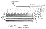
図1に示されるように、本発明の実施の形態の第1例に係る反射型LCD10は、外光入射側の基板12と対向基板14及びこれらの基板に挟み込まれた液晶層16からなる液晶セル18と、液晶セル18上に、液晶セル18から外光入射側方向へ、1/4波長板20、偏光板22、マイクロレンズフィルム24を配置し、又、液晶セル18の外光入射側の反対面に対し、光吸収層26を配置して構成される。
【0016】
外光入射側の基板12は、外光入射側から液晶層16方向へ、基材12A上に、透明電極、例えばITO(Indium Tin Oxide)12B、及び、配向膜13を積層して形成されている。
【0017】
又、対向基板14は、基材14A上に、液晶層16方向へ、配向膜13、コレステリック液晶層15、ITO14B、配向膜13が配置されている。図1ではコレステリック液晶層15上にITO14Bが形成されているが、この間に配向膜、基材を形成してもよい。
【0018】
又、対向基板14は、以下の方法で製造することができる。
【0019】
一対の基材と、各基材の内側に形成した配向膜と、該配向膜を介してコレステリック液晶層15を形成する。なお、液晶層側に配置される基材の配向膜は形成されていなくてもよい。その後、液晶層側に配置される基材もしくは基材と配向膜を剥離してカラーフィルタを形成し、その上にITO14B、配向膜13を配置し、対向基板14を構成する。このとき、基材14Aもしくは基材14Aと配向膜は剥離せず、前記のようにコレステリック液晶層15とITO14Bの間に配向膜、基材をそのまま残してもよい。
【0020】
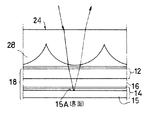
前記マイクロレンズフィルム24は、図1において下側に凸の多数のマイクロレンズ28を一体的に備えたものであり、各マイクロレンズ28は、図2に拡大して示されるように、そのレンズ焦点が、前記コレステリック液晶層15のITO14B側の界面15Aに一致するように構成されている。
【0021】
又、図1は、反射型液晶LCD10の1つの画素を示している。
【0022】
前記配向膜13は、例えばポリイミドを基材に塗布して焼成後、布でラビング処理し平行配向処理して形成され、これにより、コレステリック液晶層15や液晶層16の液晶分子は、配向膜13における配向方向に分子長軸が配向された状態となっている。
【0023】
このような構成の反射型LCD10に様々な角度の外光が入射するが、マイクロレンズフィルム24のマイクロレンズ28を通過する際に、コレステリック液晶層15への入射光の入射角度が小さくなる。即ち入射光軸が入射面の法線方向にシフトし、従来と比較して、反射光の波長の短波長側へのシフト量が小さくなる。よって、外光の入射角度の変化による色目の変化量が低減され、色純度に優れた画像を得ることができ、視野角度による色目の変化量も低減できる。
【0024】
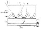
なお、前記実施の形態の例におけるマイクロレンズフィルム24は、均一の素材から形成されているが、本発明はこれに限定されるものでなく、例えば図3に示されるマイクロレンズフィルムの他の実施の形態のように、マイクロレンズの表面を一定厚さで着色した着色層34として、この部分の光透過率を変えたマイクロレンズフィルム32を用いてもよい。
【0025】
この場合、外光入射面の法線に対して所定角度の入射角を有し、外光Aのように入射した光は、図2の第1例と同様に、図3の例も、コレステリック液晶層15の界面15Aで反射する。一方、外光Bのように入射した光は、図2の第1例ではマイクロレンズフィルムで全反射し、入射方向と逆向きにランダムに出射するのに対し、図3の第2例ではマイクロレンズ34の表面を一定の厚さで着色したため、全反射をしている間に反射光が大幅に減衰し、図2の第1例に比べ、マイクロレンズフィルムによるランダムな光の反射を減少させ、視野角度による色目の変化を抑制できるのみならず、LCDの画面のコントラストを増大することができる。
【0026】
更に、マイクロレンズフィルム24、32上の表面反射を防止するため、マイクロレンズフィルム上に反射防止膜を設けてもよい。
【0027】
上記実施の形態の例における基材12A、14Aはいずれもガラス板であるが、本発明はこれに限定されるものでなく、光透過性のフィルム等であってもよい。
【0028】
又、上記反射型LCD10におけるコレステリック液晶はカイラルネマチック液晶であってもよい。
【0029】
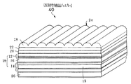
更に、上記マイクロレンズフィルムは、図1〜図3に示されるような液晶層側に凸の凸レンズであるが、これは図4に示される実施の形態の第2例の反射型LCD40のように逆向きであってもよい。なお、レンズ形状は凸レンズに限定されず、平板状のガラス基板やプラスチックシート内にレンズ作用を発生する屈折率分布を持たせて、2次元アレイ状あるいは1次元アレイ状の小さいレンズを形成した平板マイクロレンズであってもよい。
【0030】
又、前記マイクロレンズフィルム24、32は1次元方向にマイクロレンズを並列形成したものであるが、本発明はこれに限定されるものでなく、2次元アレイ状にレンズを形成したもの、例えば、蠅の目レンズ等のモザイクレンズとしてもよい。更に、1次元方向のマイクロレンズを縦横に2枚重ねてもよい。
【0031】
【実施例】
以下本発明の実施例について詳細に説明する。
【0032】
この実施例は、前記図1に示される反射型LCD10と同様の構成であり、まずその製造工程について説明する。
【0033】
適切な洗浄処理を行い、清浄とした基材としてのガラス基板上にポリイミドをスピンコートし、200℃で1時間焼成した。次に、この焼成したポリイミドに布でラビング処理を行い、厚さ約600Åの配向膜とした。
【0034】
この基板の配向膜上に溶剤(プロピレングリコールモノメチルエーテルアセテート等)で適当な粘度に希釈調整された紫外線硬化型コレステリック液晶をスピンコート法を用いて5μmの厚さに塗布し、ホットプレート上において70度で3分間のプリベークを行い、完全に溶剤を蒸発させた。
【0035】
そこに延伸処理を施したPET(ポリエチレンテレフタレート)フィルム(東レ製ルミラー25μm厚さ)を空気が入らないように、且つコレステリック液晶がはみ出さないようにしてラミネートし、所望の反射分光が得られる温度に調整した。
【0036】
次に、所望の反射分光が得られることを確認してから、フォトマスクを介して紫外線露光を行ってコレステリック液晶を硬化させた。
【0037】
ここで、上記所望の反射分光を得るための温度調整、及び、画像のパターンに対応したフォトマスクを介して紫外線露光を行う工程を必要回数だけ繰り返し、塗布したコレステリック液晶全域の露光硬化が終了した後、前記PETフィルムを剥離して、カラーフィルタとした。
【0038】
完成したカラーフィルタを用いて液晶のセル組を行った。カラーフィルタ上に1000ÅのITO膜を成膜し、その上に日本合成ゴム製ポリイミドAL1254を600Åの厚さに塗布して、200℃で1時間焼成した後に、布によりポリイミド膜表面をラビング処理して配向膜13を形成し、対向基板14とした。スペーサとして積水ファインケミカル製のSP−203を塗布し、外光入射側の基板12として、TFTを形成した基板を用いて中空セルを作成し、その後、セル中にメルク製液晶ZLI−479を注入した。これにより液晶の複屈折率と、厚みでリタデーションが起こり、入射光が液晶層16を通過することにより位相がπ変化するように調整した。
【0039】
更に、その液晶セル18の表面に市販の1/4波長板20を貼り、その進相軸に対して45°傾けて直線偏光板を貼り込んだ。又、液晶セル18の外光入射側反対面には黒い布を貼り、光吸収層26とした。
【0040】
1/4波長板20、偏光板22、光吸収26を備えた液晶セル18に光を反射させてみるとカラーフィルタの反射光が観測され、一方、電圧を印加したところ画素が黒くなり、液晶ディスプレイとして使用できることがわかった。
【0041】
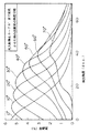
上記液晶セル上にある偏光板22上面に、図3に示されるようなレンチキュラーレンズ形状のマイクロレンズフィルム32を貼り付け、これに光を投射して、正反射の関係が反射光の測定を行ったところ、入射角度変化による反射波長の短波長側へのシフト量を減少させることができた。これは、マイクロレンズフィルム32を通ることにより、図5及び表1に示すように、全空間にわたる光の入射が、入射面に対し法線方向へシフトし、光の入射角度の変化による反射波長の短波長側へのシフト量が減少するものである。なお、図5及び表1の光検出角度はマイクロレンズフィルム32を透過した光の角度を測定しており、測定には大塚電子製LCD−5100を用いた。
【0042】
【表1】

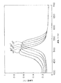
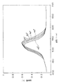
次に上記図3のマイクロレンズフィルム32の有無による、入射光角度が25°、30°、35°、40°、45°である場合の反射波長の変化を図6、7及び表2に示す。
【0044】
【表2】
図6は、マイクロレンズフィルムを備えていない反射型LCDにおける、外光の入射角に対する反射波長を示し、図7は、マイクロレンズフィルムを備えた反射型LCDにおける、外光の入射角に対する反射波長を示している。図6、図7から、マイクロレンズフィルムがない場合には、外光入射面の法線に対し入射角度が大きくなるにつれ、反射波長が短波長側にシフトするのに対し、マイクロレンズフィルムを備えた場合には、入射角度の変化による反射波長の短波長側へのシフトが減少していることがわかった。
【0046】
更に、図6、7の結果から、マイクロレンズフィルムの有無による反射光中心波長の変化を表2に示したが、マイクロレンズフィルムがない場合には、入射角度によって反射光中心波長は40nm変化しているのに対し、マイクロレンズフィルムを配置することで、反射光中心波長の変化は15nmになり、色目の変化を抑えられることがわかった。
【0047】
なお、角度は外光の入射面の法線方向からの角度で示しており、例えば入射光角度が0°というのはマイクロレンズフィルムに対し、垂直に入射しているものである。
【0048】
又、反射光中心波長とは光透過率が最大となる波長であり、測定装置には大塚電子製LCD−5100を用いた。
【0049】
【発明の効果】
本発明は上記のように構成したので、コレステリック液晶もしくはカイラルネマチック液晶からなるカラーフィルタを用いた反射型LCDにおいて、簡単な構造で、外光の入射角度の変化による色目変化を抑制し、画像のコントラスト、色純度を向上させることができるという優れた効果を有する。
【図面の簡単な説明】
【図1】本発明に実施の形態の第1例に係る反射型LCDを示す拡大略示斜視図
【図2】同要部拡大断面図
【図3】前記反射型LCDにおけるマイクロレンズフィルムの他の実施の形態を示す拡大略示断面図
【図4】同実施の形態の第2例を示す図1と同様の斜視図
【図5】本発明のマイクロレンズフィルムへの光の入射角度を変化させたときの透過光の光検出角度の変化と透過率強度との関係を示す線図
【図6】マイクロレンズフィルムを備えていない反射型LCDにおける、外光の入射角に対する反射波長を示す線図
【図7】マイクロレンズフィルムを備えた反射型LCDにおける図6と同様の線図
【符号の説明】
10、40…反射型液晶ディスプレイ
12、14…基板
15…コレステリック液晶層
15A…界面
18…液晶セル
24、32…マイクロレンズフィルム
28、34…マイクロレンズ[0001]
BACKGROUND OF THE INVENTION
The present invention relates to a reflective liquid crystal display (hereinafter referred to as LCD).
[0002]
[Prior art]
For example, as disclosed in Japanese Patent Laid-Open No. 10-282324, a color filter using a cholesteric liquid crystal or a chiral nematic liquid crystal has been proposed as a color filter for a reflective liquid crystal display.
[0003]
This color filter has superior performance in luminance and color purity compared to conventional color filters using pigments and dyes. In particular, there is an advantage that the wavelength of the selectively reflected light changes depending on the temperature, and furthermore, the use of an ultraviolet curable cholesteric liquid crystal capable of maintaining the liquid crystal state by irradiation with ultraviolet rays can be easily manufactured as compared with the conventional case.
[0004]
The cholesteric liquid crystal and chiral nematic liquid crystal as described above have a characteristic that the director spirally changes in space in addition to the long-range alignment order of the liquid crystal molecular axes. That is, in the plane parallel to the liquid crystal molecular axis, the liquid crystal has the same alignment order as the nematic phase, but when moving to the adjacent plane, this local alignment direction is slightly rotated, and this is successively continuous. And has a spiral structure.
[0005]
On the other hand, natural light can be divided into right-handed circularly polarized light and left-handed circularly polarized light. In cholesteric liquid crystal or chiral nematic liquid crystal, both right-handed circularly polarized light and left-handed circularly polarized light are parallel to the spiral axis of the liquid crystal. Is incident on the liquid crystal, it reflects only the circularly polarized light component having the same rotational direction as the twist direction of the liquid crystal, and transmits the other circularly polarized light component.
[0006]
At this time, since the phase of the reflected light does not change with respect to the incident light, the polarization direction before and after the incident of the reflected light is not changed, and the wavelength of the reflected light is equal to the twist pitch of the cholesteric liquid crystal or the chiral nematic liquid crystal. Proportional relationship. This pitch varies depending on the addition amount of a chiral agent that generates a twisting force in the liquid crystal and an appropriate external field (for example, temperature, electric field, magnetic field, etc.).
[0007]
Therefore, by controlling the above parameters in the visible range, reflected light of red, green, and blue can be formed, and the reflectance should be set higher than that of the conventional color filter. Can do.
[0008]
[Problems to be solved by the invention]
Here, the cholesteric liquid crystal or the chiral nematic liquid crystal as described above constitutes a cell while being sandwiched between two substrates, and the liquid crystal side surface of the substrate in each cell is planarly aligned. Therefore, the spiral axis of the liquid crystal is perpendicular to the substrate, and the reflected light has a regular reflection relationship in which the incident angle and the reflection angle are equal.
[0009]
However, when a reflective LCD having such a color filter is observed at an angle deviated from the front, that is, when the viewing angle changes, the wavelength of the reflected light is reduced to the short wavelength side as compared with the case of viewing from the front. There is a problem that the color tone (color eye) changes due to the shift.
[0010]
The present invention has been made in view of the above-described conventional problems, and uses a cholesteric liquid crystal or a chiral nematic liquid crystal to shift the wavelength of reflected light to the short wavelength side when the viewing angle is increased at a low cost. It is an object of the present invention to provide a reflective LCD that can be reduced.
[0011]
[Means for Solving the Problems]
The present invention, as claimed in claim 1, and a color filter formed by arranging the liquid crystal layer made of one of the cholesteric liquid crystal or chiral nematic liquid crystal on a substrate, arranged outside the light incident side of the liquid crystal layer, the outer A microlens film that shifts an incident optical axis of external light incident on the liquid crystal layer with an incident angle with respect to the normal line of the light incident surface to the normal line side on the incident surface . The above object is achieved by a reflective liquid crystal display characterized in that the surface is colored to reduce the light transmittance .
[0012]
Further, in claim 1, the lens focal point of the microlens film, may be one Itasa the interface of the external light incident side of the liquid crystal layer.
[0013]
In the present invention, the incident optical axis to the liquid crystal layer of the incident external light is shifted to the normal side of the incident surface by the microlens film disposed on the external light incident side portion of the liquid crystal layer. Shift of the wavelength to the short wavelength side is suppressed. Therefore, changes in color due to changes in the viewing angle are reduced.
[0014]
DETAILED DESCRIPTION OF THE INVENTION
Embodiments of the present invention will be described below in detail with reference to the drawings.
[0015]
As shown in FIG. 1, a
[0016]
The
[0017]
In the
[0018]
The
[0019]
A cholesteric
[0020]
The
[0021]
FIG. 1 shows one pixel of the reflective
[0022]
The
[0023]
Although external light of various angles is incident on the
[0024]
The
[0025]
In this case, the light having an incident angle of a predetermined angle with respect to the normal line of the external light incident surface and incident as the external light A is the same as the first example of FIG. Reflected at the
[0026]
Furthermore, in order to prevent surface reflection on the
[0027]
The
[0028]
The cholesteric liquid crystal in the
[0029]
Further, the microlens film is a convex lens convex on the liquid crystal layer side as shown in FIGS. 1 to 3, but this is similar to the
[0030]
The
[0031]
【Example】
Examples of the present invention will be described in detail below.
[0032]
This embodiment has the same configuration as that of the
[0033]
Appropriate cleaning treatment was performed, and a polyimide was spin-coated on a glass substrate as a cleaned base material and baked at 200 ° C. for 1 hour. Next, the fired polyimide was rubbed with a cloth to obtain an alignment film having a thickness of about 600 mm.
[0034]
An ultraviolet curable cholesteric liquid crystal diluted to an appropriate viscosity with a solvent (propylene glycol monomethyl ether acetate or the like) is applied on the alignment film of this substrate to a thickness of 5 μm using a spin coating method. Pre-baked for 3 minutes at a temperature to completely evaporate the solvent.
[0035]
Laminated PET (polyethylene terephthalate) film (Toray Lumirror 25 μm thick) so that no air enters and cholesteric liquid crystal does not protrude, and the desired reflection spectrum is obtained. Adjusted.
[0036]
Next, after confirming that a desired reflection spectrum was obtained, UV exposure was performed through a photomask to cure the cholesteric liquid crystal.
[0037]
Here, the temperature adjustment for obtaining the desired reflection spectrum and the UV exposure process through the photomask corresponding to the image pattern were repeated as many times as necessary, and the exposure and curing of the entire coated cholesteric liquid crystal was completed. Thereafter, the PET film was peeled off to obtain a color filter.
[0038]
A liquid crystal cell set was formed using the completed color filter. An ITO film of 1000 mm is formed on the color filter, and a Japanese synthetic rubber polyimide AL1254 is applied to a thickness of 600 mm and baked at 200 ° C. for 1 hour, and then the polyimide film surface is rubbed with a cloth. Thus, the
[0039]
Further, a commercially available quarter-
[0040]
When the light is reflected on the
[0041]
A microlens film 32 having a lenticular lens shape as shown in FIG. 3 is attached to the upper surface of the polarizing plate 22 on the liquid crystal cell, and light is projected onto the microlens film 32 to measure the reflected light. As a result, it was possible to reduce the shift amount of the reflected wavelength to the short wavelength side due to the change in the incident angle. As shown in FIG. 5 and Table 1, when the light passes through the microlens film 32, the incident light over the entire space shifts in the normal direction with respect to the incident surface, and the reflected wavelength due to the change in the incident angle of the light. The amount of shift to the short wavelength side is reduced. 5 and Table 1 were measured by measuring the angle of light transmitted through the microlens film 32, and an Otsuka Electronics LCD-5100 was used for the measurement.
[0042]
[Table 1]
Next, FIGS. 6 and 7 and Table 2 show changes in the reflection wavelength when the incident light angles are 25 °, 30 °, 35 °, 40 °, and 45 °, depending on the presence or absence of the microlens film 32 of FIG. .
[0044]
[Table 2]
FIG. 6 shows a reflection wavelength with respect to an incident angle of external light in a reflective LCD without a microlens film, and FIG. 7 shows a reflection wavelength with respect to an incident angle of external light in a reflective LCD with a microlens film. Is shown. 6 and 7, when there is no microlens film, the reflection wavelength shifts to the short wavelength side as the incident angle increases with respect to the normal line of the external light incident surface, whereas the microlens film is provided. In this case, it was found that the shift of the reflected wavelength toward the short wavelength side due to the change in the incident angle decreased.
[0046]
6 and 7 show changes in the reflected light center wavelength depending on the presence / absence of the microlens film. In the absence of the microlens film, the reflected light center wavelength varies by 40 nm depending on the incident angle. On the other hand, it was found that by arranging the microlens film, the change of the reflected light center wavelength becomes 15 nm, and the change of the color can be suppressed.
[0047]
The angle is indicated by an angle from the normal direction of the incident surface of the external light. For example, an incident light angle of 0 ° is perpendicular to the microlens film.
[0048]
The center wavelength of reflected light is the wavelength that maximizes the light transmittance, and Otsuka Electronics LCD-5100 was used as the measuring device.
[0049]
【The invention's effect】
Since the present invention is configured as described above, in a reflective LCD using a color filter made of cholesteric liquid crystal or chiral nematic liquid crystal, it has a simple structure and suppresses color change due to change in the incident angle of external light, and It has an excellent effect that contrast and color purity can be improved.
[Brief description of the drawings]
FIG. 1 is an enlarged schematic perspective view showing a reflective LCD according to a first example of an embodiment of the present invention. FIG. 2 is an enlarged cross-sectional view of the main part of the reflective LCD. FIG. 4 is a perspective view similar to FIG. 1 showing a second example of the embodiment. FIG. 5 changes the incident angle of light on the microlens film of the present invention. FIG. 6 is a diagram showing the relationship between the change in the light detection angle of transmitted light and the transmittance intensity when the reflection light is applied. FIG. 6 is a line showing the reflection wavelength with respect to the incident angle of external light in a reflective LCD without a microlens film. FIG. 7 is a diagram similar to FIG. 6 in a reflective LCD provided with a microlens film.
DESCRIPTION OF
Claims (2)
Priority Applications (1)
| Application Number | Priority Date | Filing Date | Title |
|---|---|---|---|
| JP11824799A JP4237331B2 (en) | 1999-04-26 | 1999-04-26 | Reflective LCD |
Applications Claiming Priority (1)
| Application Number | Priority Date | Filing Date | Title |
|---|---|---|---|
| JP11824799A JP4237331B2 (en) | 1999-04-26 | 1999-04-26 | Reflective LCD |
Publications (2)
| Publication Number | Publication Date |
|---|---|
| JP2000305074A JP2000305074A (en) | 2000-11-02 |
| JP4237331B2 true JP4237331B2 (en) | 2009-03-11 |
Family
ID=14731891
Family Applications (1)
| Application Number | Title | Priority Date | Filing Date |
|---|---|---|---|
| JP11824799A Expired - Fee Related JP4237331B2 (en) | 1999-04-26 | 1999-04-26 | Reflective LCD |
Country Status (1)
| Country | Link |
|---|---|
| JP (1) | JP4237331B2 (en) |
Families Citing this family (22)
| Publication number | Priority date | Publication date | Assignee | Title |
|---|---|---|---|---|
| JP4651791B2 (en) * | 2000-08-29 | 2011-03-16 | Nec液晶テクノロジー株式会社 | Reflective liquid crystal display device, manufacturing method thereof, and driving method thereof |
| TWI289708B (en) | 2002-12-25 | 2007-11-11 | Qualcomm Mems Technologies Inc | Optical interference type color display |
| US7342705B2 (en) | 2004-02-03 | 2008-03-11 | Idc, Llc | Spatial light modulator with integrated optical compensation structure |
| US7630123B2 (en) | 2004-09-27 | 2009-12-08 | Qualcomm Mems Technologies, Inc. | Method and device for compensating for color shift as a function of angle of view |
| US7813026B2 (en) | 2004-09-27 | 2010-10-12 | Qualcomm Mems Technologies, Inc. | System and method of reducing color shift in a display |
| US7508571B2 (en) | 2004-09-27 | 2009-03-24 | Idc, Llc | Optical films for controlling angular characteristics of displays |
| US7710636B2 (en) | 2004-09-27 | 2010-05-04 | Qualcomm Mems Technologies, Inc. | Systems and methods using interferometric optical modulators and diffusers |
| US7603001B2 (en) | 2006-02-17 | 2009-10-13 | Qualcomm Mems Technologies, Inc. | Method and apparatus for providing back-lighting in an interferometric modulator display device |
| US7845841B2 (en) | 2006-08-28 | 2010-12-07 | Qualcomm Mems Technologies, Inc. | Angle sweeping holographic illuminator |
| WO2008045207A2 (en) | 2006-10-06 | 2008-04-17 | Qualcomm Mems Technologies, Inc. | Light guide |
| CN101600901A (en) | 2006-10-06 | 2009-12-09 | 高通Mems科技公司 | Optical loss structure integrated in illumination device of display |
| WO2008045311A2 (en) | 2006-10-06 | 2008-04-17 | Qualcomm Mems Technologies, Inc. | Illumination device with built-in light coupler |
| EP1946162A2 (en) | 2006-10-10 | 2008-07-23 | Qualcomm Mems Technologies, Inc | Display device with diffractive optics |
| US7864395B2 (en) | 2006-10-27 | 2011-01-04 | Qualcomm Mems Technologies, Inc. | Light guide including optical scattering elements and a method of manufacture |
| US7777954B2 (en) | 2007-01-30 | 2010-08-17 | Qualcomm Mems Technologies, Inc. | Systems and methods of providing a light guiding layer |
| JP2008309963A (en) * | 2007-06-13 | 2008-12-25 | Hitachi Displays Ltd | Liquid crystal display device with microlens array |
| US8068710B2 (en) | 2007-12-07 | 2011-11-29 | Qualcomm Mems Technologies, Inc. | Decoupled holographic film and diffuser |
| WO2009102731A2 (en) | 2008-02-12 | 2009-08-20 | Qualcomm Mems Technologies, Inc. | Devices and methods for enhancing brightness of displays using angle conversion layers |
| WO2009102733A2 (en) | 2008-02-12 | 2009-08-20 | Qualcomm Mems Technologies, Inc. | Integrated front light diffuser for reflective displays |
| US8049951B2 (en) | 2008-04-15 | 2011-11-01 | Qualcomm Mems Technologies, Inc. | Light with bi-directional propagation |
| US8902484B2 (en) | 2010-12-15 | 2014-12-02 | Qualcomm Mems Technologies, Inc. | Holographic brightness enhancement film |
| WO2018062026A1 (en) * | 2016-09-28 | 2018-04-05 | 富士フイルム株式会社 | Optical laminated body |
-
1999
- 1999-04-26 JP JP11824799A patent/JP4237331B2/en not_active Expired - Fee Related
Also Published As
| Publication number | Publication date |
|---|---|
| JP2000305074A (en) | 2000-11-02 |
Similar Documents
| Publication | Publication Date | Title |
|---|---|---|
| JP4237331B2 (en) | Reflective LCD | |
| JP3852342B2 (en) | Reflector, reflector manufacturing method, liquid crystal device, electronic device | |
| TWI387816B (en) | Elliptical polarizer and vertical alignment type liquid crystal display device comprising the same | |
| JP3351945B2 (en) | Reflective liquid crystal display | |
| US6833891B2 (en) | Reflective liquid crystal display using cholesteric polymers | |
| US20080106676A1 (en) | Liquid Crystal Display Device | |
| TWI495943B (en) | Liquid crystal panel, driving method thereof, and liquid crystal display containing the same | |
| JPWO2009090778A1 (en) | Liquid crystal display device | |
| JP2005234204A (en) | Liquid crystal display | |
| CN102540316B (en) | Method of fabricating patterned retarder | |
| JP2003140183A (en) | Reflective liquid crystal display | |
| JP2000258760A (en) | Liquid crystal display | |
| JP2006024519A (en) | Direct type backlight and liquid crystal display device | |
| CN101509986B (en) | Wave wafer, manufacturing method, mold and liquid crystal panel | |
| JPH09113893A (en) | Reflective liquid crystal display | |
| JPH08106087A (en) | Reflection type liquid crystal display device | |
| JP2005215631A (en) | OPTICAL ELEMENT AND ITS MANUFACTURING METHOD, AND LIQUID CRYSTAL ORIENTATION SUBSTRATE AND LIQUID CRYSTAL DISPLAY | |
| JP2000330106A (en) | Electrode substrate for reflective liquid crystal display device and reflective liquid crystal display device using the same | |
| JP2001174797A (en) | Transflective liquid crystal display | |
| JP2001013528A (en) | Reflective liquid crystal display | |
| JP4324267B2 (en) | Color filter for reflective LCD | |
| JP2006024518A (en) | Direct type backlight and liquid crystal display device | |
| JP3078538B1 (en) | Manufacturing method of reflective liquid crystal display | |
| JP4912245B2 (en) | Liquid crystal display | |
| JP2003270621A (en) | Liquid crystal display |
Legal Events
| Date | Code | Title | Description |
|---|---|---|---|
| A621 | Written request for application examination |
Free format text: JAPANESE INTERMEDIATE CODE: A621 Effective date: 20060406 |
|
| A977 | Report on retrieval |
Free format text: JAPANESE INTERMEDIATE CODE: A971007 Effective date: 20080829 |
|
| A131 | Notification of reasons for refusal |
Free format text: JAPANESE INTERMEDIATE CODE: A131 Effective date: 20080909 |
|
| A521 | Written amendment |
Free format text: JAPANESE INTERMEDIATE CODE: A523 Effective date: 20081110 |
|
| TRDD | Decision of grant or rejection written | ||
| A01 | Written decision to grant a patent or to grant a registration (utility model) |
Free format text: JAPANESE INTERMEDIATE CODE: A01 Effective date: 20081216 |
|
| A01 | Written decision to grant a patent or to grant a registration (utility model) |
Free format text: JAPANESE INTERMEDIATE CODE: A01 |
|
| A61 | First payment of annual fees (during grant procedure) |
Free format text: JAPANESE INTERMEDIATE CODE: A61 Effective date: 20081218 |
|
| R150 | Certificate of patent or registration of utility model |
Free format text: JAPANESE INTERMEDIATE CODE: R150 |
|
| FPAY | Renewal fee payment (event date is renewal date of database) |
Free format text: PAYMENT UNTIL: 20111226 Year of fee payment: 3 |
|
| FPAY | Renewal fee payment (event date is renewal date of database) |
Free format text: PAYMENT UNTIL: 20121226 Year of fee payment: 4 |
|
| FPAY | Renewal fee payment (event date is renewal date of database) |
Free format text: PAYMENT UNTIL: 20121226 Year of fee payment: 4 |
|
| FPAY | Renewal fee payment (event date is renewal date of database) |
Free format text: PAYMENT UNTIL: 20131226 Year of fee payment: 5 |
|
| LAPS | Cancellation because of no payment of annual fees |