JP4236713B2 - Storage device and access method - Google Patents
Storage device and access method Download PDFInfo
- Publication number
- JP4236713B2 JP4236713B2 JP20437397A JP20437397A JP4236713B2 JP 4236713 B2 JP4236713 B2 JP 4236713B2 JP 20437397 A JP20437397 A JP 20437397A JP 20437397 A JP20437397 A JP 20437397A JP 4236713 B2 JP4236713 B2 JP 4236713B2
- Authority
- JP
- Japan
- Prior art keywords
- address
- data
- bank
- pixels
- memory
- Prior art date
- Legal status (The legal status is an assumption and is not a legal conclusion. Google has not performed a legal analysis and makes no representation as to the accuracy of the status listed.)
- Expired - Fee Related
Links
Images
Classifications
-
- G—PHYSICS
- G06—COMPUTING; CALCULATING OR COUNTING
- G06F—ELECTRIC DIGITAL DATA PROCESSING
- G06F12/00—Accessing, addressing or allocating within memory systems or architectures
-
- G—PHYSICS
- G09—EDUCATION; CRYPTOGRAPHY; DISPLAY; ADVERTISING; SEALS
- G09G—ARRANGEMENTS OR CIRCUITS FOR CONTROL OF INDICATING DEVICES USING STATIC MEANS TO PRESENT VARIABLE INFORMATION
- G09G5/00—Control arrangements or circuits for visual indicators common to cathode-ray tube indicators and other visual indicators
- G09G5/36—Control arrangements or circuits for visual indicators common to cathode-ray tube indicators and other visual indicators characterised by the display of a graphic pattern, e.g. using an all-points-addressable [APA] memory
- G09G5/39—Control of the bit-mapped memory
-
- H—ELECTRICITY
- H04—ELECTRIC COMMUNICATION TECHNIQUE
- H04N—PICTORIAL COMMUNICATION, e.g. TELEVISION
- H04N19/00—Methods or arrangements for coding, decoding, compressing or decompressing digital video signals
- H04N19/42—Methods or arrangements for coding, decoding, compressing or decompressing digital video signals characterised by implementation details or hardware specially adapted for video compression or decompression, e.g. dedicated software implementation
- H04N19/423—Methods or arrangements for coding, decoding, compressing or decompressing digital video signals characterised by implementation details or hardware specially adapted for video compression or decompression, e.g. dedicated software implementation characterised by memory arrangements
-
- H—ELECTRICITY
- H04—ELECTRIC COMMUNICATION TECHNIQUE
- H04N—PICTORIAL COMMUNICATION, e.g. TELEVISION
- H04N19/00—Methods or arrangements for coding, decoding, compressing or decompressing digital video signals
- H04N19/50—Methods or arrangements for coding, decoding, compressing or decompressing digital video signals using predictive coding
- H04N19/59—Methods or arrangements for coding, decoding, compressing or decompressing digital video signals using predictive coding involving spatial sub-sampling or interpolation, e.g. alteration of picture size or resolution
-
- G—PHYSICS
- G09—EDUCATION; CRYPTOGRAPHY; DISPLAY; ADVERTISING; SEALS
- G09G—ARRANGEMENTS OR CIRCUITS FOR CONTROL OF INDICATING DEVICES USING STATIC MEANS TO PRESENT VARIABLE INFORMATION
- G09G2340/00—Aspects of display data processing
- G09G2340/02—Handling of images in compressed format, e.g. JPEG, MPEG
-
- H—ELECTRICITY
- H04—ELECTRIC COMMUNICATION TECHNIQUE
- H04N—PICTORIAL COMMUNICATION, e.g. TELEVISION
- H04N19/00—Methods or arrangements for coding, decoding, compressing or decompressing digital video signals
- H04N19/30—Methods or arrangements for coding, decoding, compressing or decompressing digital video signals using hierarchical techniques, e.g. scalability
- H04N19/39—Methods or arrangements for coding, decoding, compressing or decompressing digital video signals using hierarchical techniques, e.g. scalability involving multiple description coding [MDC], i.e. with separate layers being structured as independently decodable descriptions of input picture data
Landscapes
- Engineering & Computer Science (AREA)
- Theoretical Computer Science (AREA)
- Multimedia (AREA)
- Signal Processing (AREA)
- General Physics & Mathematics (AREA)
- Physics & Mathematics (AREA)
- Computer Hardware Design (AREA)
- General Engineering & Computer Science (AREA)
- Compression Or Coding Systems Of Tv Signals (AREA)
- Dram (AREA)
- Image Input (AREA)
- Storing Facsimile Image Data (AREA)
- Image Processing (AREA)
- Memory System (AREA)
- Compression Of Band Width Or Redundancy In Fax (AREA)
- Control Of Indicators Other Than Cathode Ray Tubes (AREA)
- Controls And Circuits For Display Device (AREA)
Description
【0001】
【発明の属する技術分野】
本発明は、記憶装置およびアクセス方法に関し、特に、例えば、画像を、画素数の異なる複数の階層に分割する階層符号化を行う場合などに用いて好適な記憶装置およびアクセス方法に関する。
【0002】
【従来の技術】
例えば、高解像度の画像データを、最下位階層または第1の階層の画像データとして、それより画素数の少ない第2の階層の画像データを形成し、さらに、それより画素数の少ない第3の階層の画像データを形成し、以下、同様にして、最上位階層までの画像データを形成する符号化手法がある。このような符号化は、階層符号化と呼ばれ、各階層の画像データは、その階層に対応した解像度(画素数)のモニタで表示される。従って、ユーザ側では、階層符号化された画像データのうち、自身が有するモニタの解像度に対応するものを選択することで、その画像データを視聴することができる。
【0003】
ところで、ある解像度の画像データを最下位階層(第1階層)の画像データとして、上位階層の画像データを、順次形成し、それらのすべてを、そのまま記憶や伝送などする場合には、最下位階層の画像データだけを記憶等する場合に比較して、上位階層の画像データの分だけ、記憶容量や伝送容量が余計に必要となる。
【0004】
そこで、そのような記憶容量等の増加を低減する階層符号化方法を、本件出願人は先に提案している。
【0005】
即ち、例えば、いま、2×2画素(横×縦)の4画素の加算値を、上位階層の画素(画素値)とし、3階層の階層符号化を行うものとする。この場合、いま、最下位階層の画像として、例えば、図9(A)に示すように、8×8画素を考えると、その左上の2×2画素の4画素h00,h10,h01,h11の加算値m0が演算され、これが、第2階層の左上の1画素とされる。同様にして、最下位階層の画像の右上の4画素h20,h31,h21,h31の加算値m1、左下の4画素h02,h12,h03,h13の加算値m2、右下の4画素h22,h32,h23,h33の加算値m3が演算され、それぞれが、第2階層の右上、左下、右下の1画素とされる。そして、第2階層の2×2画素の4画素m0,m1,m2,m3の加算値q0が演算され、これが、第3階層、即ち、ここでは、最上位階層の画像の画素とされる。
【0006】
以上の画素h00乃至h33,m0乃至m3,q0を、そのまま全部記憶などさせたのでは、上述のように、第2階層の画素m0乃至m3、および第3階層のq0の分だけ余分に記憶容量等が必要となる。
【0007】
そこで、図9(B)に示すように、第3階層の画素q0を、第2階層の画素m0乃至m3のうちの、例えば、右下の画素m3の位置に配置する。これにより、第2の階層は、画素m0乃至m2およびq0で構成されることになる。
【0008】
そして、図9(C)に示すように、第2の階層の画素m0を、それを求めるのに用いた第1の階層の画素h00,h10,h01,h11のうちの、例えば、右下の画素h11の位置に配置する。第2の階層の残りの画素m1,m2,q0も、同様に、第1階層の画素h31,h13,h33に代えて配置する。なお、画素q0は、画素h22,h32,h23,h33から直接求められたものではないが、それらから直接求められたm3に代えて第2階層に配置されているものであるから、画素h33の位置に画素m3を配置する代わりに、画素q0を配置する。
【0009】
以上のようにすることで、図9(C)に示すように、全画素数は4×4の16画素となり、図9(A)に示した最下位階層の画素だけの場合と変わらない。従って、この場合、記憶容量等の増加を低減することができる。
【0010】
なお、画素q0と代えられた画素m3およびh33、画素m0乃至m2とそれぞれ代えられた画素h11,h31,h13の復号は、次のようにして行うことができる。
【0011】
即ち、q0は、m0乃至m3の加算値であるから、式q0=m0+m1+m2+m3が成り立つ。従って、式m3=q0−(m0+m1+m2)により、m3を求めることができる。
【0012】
また、m0は、h00,h10,h01,h11の加算値であるから、式m0=h00+h10+h01+h11が成り立つ。従って、式h11=m0−(h00+h10+h01)により、h11を求めることができる。同様にして、h31,h13,h33も求めることができる。なお、h33は、上述したようにしてm3を求めてから求めることになる。
【0013】
【発明が解決しようとする課題】
ところで、以上のような階層符号化は、従来においては、その階層符号化結果を記憶する汎用的なメモリ(例えば、SRAM(Static Random Access Memory)やDRAM(Dynamic RAM)など)の他に、第1階層の画素(画素値)のラインディレイを行うための遅延回路などが必要であった。
【0014】
即ち、例えば、図9(C)に示した場合において、記憶等がされない第1階層の画素h11を求めるためには、式h11=m0−(h00+h10+h01)を演算する必要があるが、この場合、1ライン目の画素h00,h10と、2ライン目の画素h01,m0が必要になる。いま、メモリからの画像データの読み出しが、ライン単位で、上から下の方向に順次行われるとすると、h00で始まるラインを、1ライン分遅延し、h01で始まるラインが読み出されるのを待って、即ち、画素h11を計算するのに必要な、画素m0,h00,h10,h01が読み出されるのを待って、画素h11を計算する必要がある。
【0015】
このように、従来においては、メモリの他に、画像データのラインディレイを行う遅延回路が必要であり、装置が大型化する課題があった。
【0016】
本発明は、このような状況に鑑みてなされたものであり、装置の小型化などを図ることができるようにするものである。
【0017】
【課題を解決するための手段】
請求項1に記載の記憶装置は、その記憶領域へアクセスするためのアドレス空間が、記憶領域において異なる複数の範囲をさすように複数のブロックに分割され、各ブロックごとに、その記憶領域に記憶される入力画像データを構成する画素のうちの、後記第2の記憶手段に記憶される画素を除く画素のそれぞれについてアドレス指定が可能な第1の記憶手段と、その記憶領域へアクセスするためのアドレス空間が、第1の記憶手段の記憶領域へアクセスするためのアドレス空間を構成するブロックと同一の数のブロックに分割され、各ブロックごとに、その記憶領域に記憶される階層データを構成する画素単位でアドレス指定が可能な第2の記憶手段と、各ブロックに対応するアドレス指定情報に基づいて、第1の記憶手段の各ブロックそれぞれに対するアドレス指定を同時に行うとともに、アドレス指定情報を構成するビット列の一部によって第2の記憶手段の各ブロックそれぞれに対するアドレス指定を同時に行うアドレス指定手段と、入力画像データを構成する画素のうち、所定の位置の複数の画素の画素値を順次加算することにより階層データを算出する第1の処理と、入力画像データを構成する画素のうち、所定の位置の複数の画素の画素値を階層データから順次減算することにより入力画像データを構成する画素の画素値を算出する第2の処理を同時に実行する読み書き手段とを備え、第1の処理において読み書き手段は、アドレス指定情報により指定された第2の記憶手段のブロックに含まれる各アドレスに対応する第1の記憶手段の複数のアドレスそれぞれに書き込まれるデータの加算値を求めて、階層データを算出する処理途中のデータである第1の処理データを、第2の記憶手段の各アドレスに書き込み、第2の処理において読み書き手段は、アドレス指定情報により指定された第1の記憶手段のブロックに含まれるアドレスに記憶されている入力画像データを読み出すとともに、アドレス指定情報に基づいて特定される第2の記憶手段の、第1の処理データを読み出し、その入力画像データを第1の処理データから減算することにより、第1の記憶手段に記憶されていない入力画像データを算出する処理途中のデータである第2の処理データを算出し、その第2の処理データを、第1の処理データが記憶されていた第2の記憶手段のアドレスに書き込むことを特徴とする。
【0018】
請求項4に記載のアクセス方法は、アドレス指定情報により指定された第2の記憶手段のブロックに含まれる各アドレスに対応する第1の記憶手段の複数のアドレスそれぞれに書き込まれるデータの加算値を求めて、階層データを算出する処理途中のデータである第1の処理データを、第2の記憶手段の各アドレスに書き込む第1の処理と、第2の処理において読み書き手段は、アドレス指定情報により指定された第1の記憶手段のブロックに含まれるアドレスに記憶されている入力画像データを読み出すとともに、アドレス指定情報に基づいて特定される第2の記憶手段の、第1の処理データを読み出し、その入力画像データを第1の処理データから減算することにより、第1の記憶手段に記憶されていない入力画像データを算出する処理途中のデータである第2の処理データを算出し、その第2の処理データを、第1の処理データが記憶されていた第2の記憶手段のアドレスに書き込む第2の処理とを同時に実行することを特徴とする。
【0019】
請求項1に記載の記憶装置においては、第1の記憶手段は、その記憶領域へアクセスするためのアドレス空間が、記憶領域において異なる複数の範囲をさすように複数のブロックに分割され、各ブロックごとに、その記憶領域に記憶される入力画像データを構成する画素のうちの、後記第2の記憶手段に記憶される画素を除く画素のそれぞれについてアドレス指定が可能なようになされている。アドレス指定手段は、各ブロックに対応するアドレス指定情報に基づいて、第1の記憶手段の各ブロックそれぞれに対するアドレス指定を同時に行うとともに、アドレス指定情報を構成するビット列の一部によって第2の記憶手段の各ブロックそれぞれに対するアドレス指定を同時に行い、第2の記憶手段は、その記憶領域へアクセスするためのアドレス空間が、第1の記憶手段の記憶領域へアクセスするためのアドレス空間を構成するブロックと同一の数のブロックに分割され、各ブロックごとに、その記憶領域に記憶される階層データを構成する画素単位でアドレス指定が可能なようになされている。読み書き手段は、各ブロックに対応するアドレス指定情報に基づいて、第1の記憶手段の各ブロックそれぞれに対するアドレス指定を同時に行うとともに、アドレス指定情報を構成するビット列の一部によって第2の記憶手段の各ブロックそれぞれに対するアドレス指定を同時に行うアドレス指定手段と、入力画像データを構成する画素のうち、所定の位置の複数の画素の画素値を順次加算することにより階層データを算出する第1の処理と、入力画像データを構成する画素のうち、所定の位置の複数の画素の画素値を階層データから順次減算することにより入力画像データを構成する画素の画素値を算出する第2の処理を同時に実行するようになされている。
【0020】
請求項4に記載のアクセス方法においては、アドレス指定情報により指定された第2の記憶手段のブロックに含まれる各アドレスに対応する第1の記憶手段の複数のアドレスそれぞれに書き込まれるデータの加算値を求めて、階層データを算出する処理途中のデータである第1の処理データを、第2の記憶手段の各アドレスに書き込む第1の処理と、アドレス指定情報により指定された第1の記憶手段のブロックに含まれるアドレスに記憶されている入力画像データを読み出すとともに、アドレス指定情報に基づいて特定される第2の記憶手段の、第1の処理データを読み出し、その入力画像データを第1の処理データから減算することにより、第1の記憶手段に記憶されていない入力画像データを算出する処理途中のデータである第2の処理データを算出し、その第2の処理データを、第1の処理データが記憶されていた第2の記憶手段のアドレスに書き込む第2の処理とが同時に実行される。
【0026】
【発明の実施の形態】
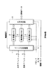
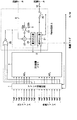
図1は、本発明を適用した記憶装置の一実施の形態の構成例を示している。
【0027】
この記憶装置は、例えば、1チップのCMOS(Complementary Metal Oxide Semiconductor)などで構成され、そこに入力される入力画像から画素数の異なる、例えば、3階層の画像を形成する階層符号化を行うようになされている。
【0028】
即ち、アドレス供給回路1には、記憶装置に入力される画像を構成する画素の水平方向または垂直方向の位置に対応したアドレスそれぞれとしての水平アドレスまたは垂直アドレスが供給されるようになされている。
【0029】
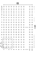
なお、本実施の形態では、例えば、図2に示すような、水平方向が512画素で、垂直方向が512ラインで1画面が構成される画像(ディジタル画像データ)が入力されるものとする。従って、水平アドレスおよび垂直アドレスは、いずれも9(=log2512)ビットで表される。
【0030】
アドレス供給回路1は、そこに供給される水平アドレスおよび垂直アドレスを必要に応じて加工して、第1階層メモリ2、第2階層メモリ3、および第3階層メモリ4に供給するようになされている。なお、アドレス供給回路1には、水平アドレスおよび垂直アドレスの他、クロック(後述する図3乃至図6および図8においては図示せず)、R/W(Read/Write)信号、および階層フラグも供給されるようになされており、アドレス供給回路1は、そのクロックに同期して、第1階層メモリ2、第2階層メモリ3、および第3階層メモリ4にアドレスを供給するようになされている。また、アドレス供給回路1は、R/W信号や階層フラグに対応して、そこに供給される水平アドレスおよび垂直アドレスを加工するようになされている。さらに、アドレス供給回路1は、必要に応じて、所定の制御信号を、RMW回路5に供給するようになされている。
【0031】
ここで、R/W信号は、記憶装置からの画像データの読み出し、または記憶装置への画像データの書き込みを指示する信号であり、階層フラグは、記憶装置に記憶された画像を読み出す場合に、後述する第1乃至第3階層の画像のうちのいずれを読み出すかを指示するための、例えば2ビットのフラグである。なお、画像データの書き込みは、例えば、第1階層メモリ2、第2階層メモリ3、および第3階層メモリ4に対して同時に行われるようになされており、従って、R/W信号が書き込みを表している場合は、階層フラグは無視される(意味をもたない)。また、読み出しは、第1階層メモリ2、第2階層メモリ3、第3階層メモリ4それぞれについて個別に行われるようになされており、従って、階層フラグは、読み出し時においてのみ有効となる。但し、第1階層メモリ2、第2階層メモリ3、第3階層メモリ4からの読み出しも同時に行うようにすることが可能である。この場合、階層フラグは用いる必要がない。
【0032】
第1階層メモリ2は、アドレス供給回路1によって指定されるアドレスに、RMW回路5から供給される画像データを記憶し、また、そのアドレスに記憶されている画像データを読み出してRMW回路5に出力するようになされている。なお、第1階層メモリ2は、第1階層の画像、即ち、ここでは、記憶装置に入力される画像データをそのまま記憶するようになされている。また、第1階層メモリ2は、少なくとも、1画面分の第1階層の画像、即ち、ここでは、図2に示したように、512×512画素の画像データを記憶することができるようになされている。さらに、第1階層メモリ2を構成するメモリセルは、少なくとも、第1階層の画像を構成する画素に割り当てられたビット数と同一のデータ長を有している。即ち、第1階層の画像を構成する画素が、例えば、8ビットで表されるとき、第1階層メモリ2を構成するメモリセルは、少なくとも8ビットのデータ長を有している。
【0033】
第2階層メモリ3は、アドレス供給回路1によって指定されるアドレスに、RMW回路5から供給される画像データを記憶し、また、そのアドレスに記憶されている画像データを読み出してRMW回路5に出力するようになされている。なお、第2階層メモリ3は、第2階層の画像を記憶するようになされている。即ち、本実施の形態では、例えば、図9における場合と同様にして、第1階層の画像を構成する2×2(横×縦)の4画素から、第2階層の1の画素が形成されるようになされており、第2階層メモリ3は、そのような画素で構成される第2階層の画像を記憶するようになされている。また、第2階層メモリ3は、少なくとも、1画面分の第2階層の画像を記憶することのできる記憶容量を有している。即ち、ここでは、第1階層の2×2画素から第2階層の1の画素が形成されるから、第2階層の画像の1画面は、256×256(=512/2×512/2)画素で構成されることになる。従って、第2階層メモリ2は、そのような数の画素数で構成される第2階層の画像を、少なくとも記憶することができるようになされている。さらに、第2階層メモリ3を構成するメモリセルは、少なくとも、第2階層の画像を構成する画素を桁落ちさせずに記憶することのできるデータ長を有している。即ち、本実施の形態では、第1階層の画素が8ビットで表されるから、そのような8ビットの画素の4つの加算値である第2階層の画素は10(=log2(28+28+28+28))ビットで表されることになる。従って、第2階層メモリ3を構成するメモリセルは、少なくとも10ビットのデータ長を有している。
【0034】
第3階層メモリ4は、アドレス供給回路1によって指定されるアドレスに、RMW回路5から供給される画像データを記憶し、また、そのアドレスに記憶されている画像データを読み出してRMW回路5に出力するようになされている。なお、第3階層メモリ4は、第3階層の画像を記憶するようになされている。即ち、本実施の形態では、例えば、図9における場合と同様にして、第2階層の画像を構成する2×2の4画素、従って、第1階層の画像を構成する4×4画素から、第3階層の1の画素が形成されるようになされており、第3階層メモリ4は、そのような画素で構成される第3階層の画像を記憶するようになされている。また、第3階層メモリ4は、少なくとも、1画面分の第3階層の画像を記憶することのできる記憶容量を有している。即ち、ここでは、第2階層の2×2画素から第3階層の1の画素が形成されるから、第2階層の画像の1画面は、128×128(=256/2×256/2)画素で構成されることになる。従って、第3階層メモリ4は、そのような数の画素数で構成される第3階層の画像を、少なくとも記憶することができるようになされている。さらに、第3階層メモリ4を構成するメモリセルは、少なくとも、第3階層の画像を構成する画素を桁落ちさせずに記憶することができるデータ長を有している。即ち、本実施の形態では、第2階層の画素が、上述したように10ビットで表されるから、そのような10ビットの画素の4つの加算値である第3階層の画素は12(=log2(210+210+210+210))ビットで表されることになる。従って、第3階層メモリ4を構成するメモリセルは、少なくとも12ビットのデータ長を有している。
【0035】
なお、第1階層メモリ2、第2階層メモリ3、および第3階層メモリ4には、クロックが供給されるようになされており、このクロックに同期して、データの読み書きが行われるようになされている。
【0036】
RMW回路5は、記憶装置に供給される画像データを、第1階層の画像として、第1階層メモリ2に書き込むようになされている。また、RMW回路5は、第1階層の画像から第2階層の画像を算出する処理を行い、第2階層メモリ3に書き込むようになされている。さらに、RMW回路5は、第1階層の画像(または第2階層の画像)から第3階層の画像を算出する処理を行い、第3階層メモリ4に書き込むようになされている。また、RMW回路5は、第1階層メモリ2、第2階層メモリ3、または第3階層メモリ4にそれぞれ記憶された画像データを読み出して出力するようにもなされている。なお、RMW回路5には、クロック、R/W信号、階層フラグ、アドレス供給回路1が出力する制御信号が供給されるようになされており、RMW回路5は、クロックに同期し、R/W信号、階層フラグ、制御信号に基づいて各種の処理を行うようになされている。
【0037】
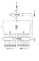
次に、その動作について、図3乃至図5を参照して説明する。
【0038】
なお、ここでは、上述の図2に示したように、1画面が512×512画素で構成され、各画素が8ビットで表される画像データが、第1階層の画像として記憶装置に供給されるものとする。また、画像データは、いわゆる順次走査されて供給されるものとする。
【0039】
さらに、第1階層の画像を構成する画素を、その最も左上の画素をh(0,0)とし、以下、同様にして、左からx+1番目で、上からy+1番目にある画素をh(x,y)と表す。第1階層の画像は、上述したように、512×512画素で構成されるから、x,yは、いずれも0乃至511(=29−1)の範囲の整数値をとる。
【0040】
また、0乃至255(=29/2−1)の範囲の整数値をとる変数s,tを考えると、第2階層の画像を構成する画素は、第1階層の隣接する2×2画素
h(2s,2t), h(2s+1,2t),
h(2s,2t+1),h(2s+1,2t+1)
の加算値となるが、それをm(s,t)と表す。従って、式
m(s,t)=h(2s,2t)+h(2s+1,2t)+h(2s,2t+1)+h(2s+1,2t+1)・・・(1)
が成り立つ。
【0041】
さらに、0乃至127(=29/4−1)の範囲の整数値をとる変数m,nを考えると、第3階層の画像を構成する画素は、第2階層の隣接する2×2画素
m(2m,2n), m(2m+1,2n),
m(2m,2n+1),m(2m+1,2n+1)
の加算値、即ち、第1階層の隣接する4×4画素
h(4m,4n), h(4m+1,4n), h(4m+2,4n), h(4m+3,4n),
h(4m,4n+1),h(4m+1,4n+1),h(4m+2,4n+1),h(4m+3,4n+1),
h(4m,4n+2),h(4m+1,4n+2),h(4m+2,4n+2),h(4m+3,4n+2),
h(4m,4n+3),h(4m+1,4n+3),h(4m+2,4n+3),h(4m+3,4n+3)
の加算値となるが、それをq(m,n)と表す。従って、式
q(m,n)=m(2m,2n)+m(2m+1,2n)+m(2m,2n+1)+m(2m+1,2n+1)
=h(4m,4n)+h(4m+1,4n)+h(4m+2,4n)+h(4m+3,4n)
+h(4m,4n+1)+h(4m+1,4n+1)+h(4m+2,4n+1)+h(4m+3,4n+1)
+h(4m,4n+2)+h(4m+1,4n+2)+h(4m+2,4n+2)+h(4m+3,4n+2)
+h(4m,4n+3)+h(4m+1,4n+3)+h(4m+2,4n+3)+h(4m+3,4n+3)・・・(2)
が成り立つ。
【0042】
また、アドレス供給回路1には、データの書き込み時および読み出し時のいずれの場合も、水平アドレスHAおよび垂直アドレスVAの組合せ(HA,VA)が、例えば、
(0,0),(1,0),・・・,(511,0),
(0,1),(1,1),・・・,(511,1),
・
・
・
(511,0),(511,1),・・・,(511,511)
の順(順次走査に対応する順)で、クロックに同期して供給されるものとする。
【0043】
さらに、9ビットの水平アドレスHAの各ビットを、その最下位ビットをha0として、ha1,ha2,・・・,ha8(ha8は最上位ビット)と表すとともに、9ビットの垂直アドレスVAの各ビットも同様に、その最下位ビットをva0として、va1,va2,・・・,va8(va8は最上位ビット)と表す。
【0044】
また、記憶装置への画像データの書き込み時には、RMW回路5には、第1階層の画像が、クロックに同期して順次走査されて供給され、これに伴い、アドレス供給回路1には、水平アドレスHAおよび垂直アドレスVAが、上述したように供給されるものとする。
【0045】
この場合、第1階層メモリ2へのアクセスは、次のようにして行われる。
【0046】
即ち、図3に示すように、まず書き込み時(R/W信号が書き込みを表している場合)においては、アドレス供給回路1は、そこに供給される水平アドレスHAおよび垂直アドレスVAを、そのまま、第1階層メモリ2のアドレス端子(ADh,ADv)に供給する。一方、RMW回路5は、そこに供給される第1階層の画像データを、水平アドレスHAおよび垂直アドレスVAによって指定されている第1階層メモリ2のメモリセル(図示せず)に書き込む。以下、同様の処理が行われることで、512×512画素で構成される1画面分の第1階層の画像が、第1階層メモリ2に記憶される。即ち、これにより、第1階層メモリ2のアドレス
(0,0),(1,0),・・・,(511,0),
(0,1),(1,1),・・・,(511,1),
・・・
(511,0),(511,1),・・・,(511,511)
には、第1階層の画素(画素値)
h(0,0),h(1,0),・・・,h(511,0),
h(0,1),h(1,1),・・・,h(511,1),
・・・
h(511,0),h(511,1),・・・,h(511,511)
がそれぞれ記憶される。
【0047】
読み出し時(R/W信号が読み出しを表している場合)においては、アドレス供給回路1は、階層フラグが第1階層を表していれば、やはり、そこに供給される水平アドレスHAおよび垂直アドレスVAを、そのまま、第1階層メモリ2のアドレス端子に供給する。そして、RMW回路5は、水平アドレスHAおよび垂直アドレスVAによって指定されている第1階層メモリ2のメモリセルに記憶されている第1階層の画像データを読み出し、以下、同様の処理が行われることで、512×512画素で構成される1画面分の第1階層の画像が、第1階層メモリ2から読み出される。即ち、これにより、順次走査された第1階層の画像が出力される。
【0048】
次に、第2階層メモリ3へのアクセスについて説明する。
【0049】
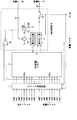
まず書き込み時においては、アドレス供給回路1は、例えば、図4に示すように、そこに供給される水平アドレスHAの一部としての、そのうちの最下位ビットha0を除く上位8ビットha1乃至ha8と、垂直アドレスVAの一部としての、最下位ビットva0を除く上位8ビットva1乃至va8を、第2階層メモリ3のアドレス端子に供給する。さらに、アドレス供給回路1は、水平アドレスHAの最下位ビットha0と、垂直アドレスVAの最下位ビットva0を、制御信号として、RMW回路5に出力する。
【0050】
従って、例えば、図2にD1で示すような第1階層の2×2の4画素h(2s,2t),h(2s+1,2t),h(2s,2t+1),h(2s+1,2t+1)が、RMW回路5に供給されるタイミングにおいては、いずれのタイミングでも、アドレス供給回路1は、第2階層メモリ3の同一アドレス(s,t)を指定する信号を、第2階層メモリ3に出力する。
【0051】
一方、RMW回路5では、そこに供給される第1階層の画像データが、演算器13に入力される。演算器13には、第1階層の画像データの他、スイッチ12の出力が供給されるようになされており、演算器13は、それらを加算して、書き込み部14に供給するようになされている。
【0052】
スイッチ12は、NORゲート15の出力に対応して、端子12aまたは12bのうちのいずれか一方を選択するようになされており、また、端子12aまたは12bには、読み出し部11の出力または0がそれぞれ供給されるようになされている。NORゲート15には、アドレス供給回路1からの水平アドレスHAの最下位ビットha0と、垂直アドレスVAの最下位ビットva0とが供給されるようになされており、従って、その出力は、最下位ビットha0およびva0がいずれも0の場合、即ち、第1階層の2×2画素h(2s,2t),h(2s+1,2t),h(2s,2t+1),h(2s+1,2t+1)のうちの左上の画素h(2s,2t)が、演算器13に供給されるタイミングの場合のみ、Hレベルとなり、他の場合はLレベルとなるようになされている。
【0053】
そして、スイッチ12は、NORゲート15の出力がLレベルまたはHレベルのとき、端子12aまたは12bをそれぞれ選択するようになされている。
【0054】
また、読み出し部11は、アドレス供給回路1が出力する信号に対応するアドレスに記憶されているデータ(記憶データ)を読み出すようになされている。
【0055】
従って、第1階層の2×2画素h(2s,2t),h(2s+1,2t),h(2s,2t+1),h(2s+1,2t+1)のうちの左上の画素h(2s,2t)が演算器13に供給されるタイミングにおいては、読み出し部11において、第2階層メモリ3のアドレス(s,t)に記憶されたデータが読み出され、端子12aに供給されるが、この場合、水平アドレスHAの最下位ビットha0、および垂直アドレスVAの最下位ビットva0はいずれも0であるから、NORゲート15の出力はHレベルとなり、スイッチ12は端子12bを選択する。
【0056】
その結果、演算器13には、スイッチ12を介して0が供給される。
【0057】
演算器13では、この0と第1階層の画素h(2s,2t)とが加算され、その加算値(0+h(2s,2t))が、書き込み部14に供給される。書き込み部14は、演算器13の出力を、アドレス供給回路1が出力する信号に対応するアドレス、即ち、第2階層メモリ3のアドレス(s,t)に書き込む。
【0058】
次に、第1階層の2×2画素h(2s,2t),h(2s+1,2t),h(2s,2t+1),h(2s+1,2t+1)のうちの左上の画素h(2s,2t)の右隣の画素h(2s+1,2t)が演算器13に供給されるタイミングにおいては、読み出し部11において、やはり、第2階層メモリ3のアドレス(s,t)に記憶されたデータ(ここでは、0+h(2s,2t))が読み出され、端子12aに供給される。
【0059】
一方、この場合、水平アドレスHAの最下位ビットha0は1で、垂直アドレスVAの最下位ビットva0は0となっているから、NORゲート15の出力はLレベルとなり、スイッチ12は端子12aを選択する。
【0060】
その結果、演算器13には、スイッチ12を介して、読み出し部11において読み出されたデータ(記憶データ)(ここでは、0+h(2s,2t))が供給される。
【0061】
演算器13では、スイッチ12を介して供給されるデータと、第1階層の画素h(2s+1,2t)とが加算され、その加算値(0+h(2s,2t)+h(2s+1,2t))が、書き込み部14に供給される。書き込み部14は、演算器13の出力を、アドレス供給回路1が出力する信号に対応するアドレス、即ち、第2階層メモリ3のアドレス(s,t)に書き込む。
【0062】
その後、第1階層の上から2t+1ライン目の画像データの供給が開始され、第1階層の2×2画素h(2s,2t),h(2s+1,2t),h(2s,2t+1),h(2s+1,2t+1)のうちの左下の画素h(2s,2t+1)が、演算器13に供給されると、読み出し部11において、やはり、第2階層メモリ3のアドレス(s,t)に記憶されたデータ(ここでは、0+h(2s,2t)+h(2s+1,2t))が読み出され、端子12aに供給される。
【0063】
一方、この場合、水平アドレスHAの最下位ビットha0は0で、垂直アドレスVAの最下位ビットva0は1となっているから、NORゲート15の出力はLレベルとなり、スイッチ12は端子12aを選択する。
【0064】
その結果、演算器13には、スイッチ12を介して、読み出し部11において読み出されたデータ(記憶データ)(ここでは、0+h(2s,2t)+h(2s+1,2t))が供給される。
【0065】
演算器13では、スイッチ12を介して供給されるデータと、第1階層の画素h(2s,2t+1)とが加算され、その加算値(0+h(2s,2t)+h(2s+1,2t)+h(2s,2t+1))が、書き込み部14に供給される。書き込み部14は、演算器13の出力を、アドレス供給回路1が出力する信号に対応するアドレス、即ち、第2階層メモリ3のアドレス(s,t)に書き込む。
【0066】
次に、第1階層の2×2画素h(2s,2t),h(2s+1,2t),h(2s,2t+1),h(2s+1,2t+1)のうちの左下の画素h(2s,2t+1)の右隣の画素h(2s+1,2t+1)が、演算器13に供給されると、読み出し部11において、やはり、第2階層メモリ3のアドレス(s,t)に記憶されたデータ(ここでは、0+h(2s,2t)+h(2s+1,2t)+h(2s,2t+1))が読み出され、端子12aに供給される。
【0067】
一方、この場合、水平アドレスHAの最下位ビットha0および垂直アドレスVAの最下位ビットva0は、いずれも1となっているから、NORゲート15の出力はLレベルとなり、スイッチ12は端子12aを選択する。
【0068】
その結果、演算器13には、スイッチ12を介して、読み出し部11において読み出されたデータ(記憶データ)(ここでは、0+h(2s,2t)+h(2s+1,2t)+h(2s,2t+1))が供給される。
【0069】
演算器13では、スイッチ12を介して供給されるデータと、第1階層の画素h(2s+1,2t+1)とが加算され、その加算値(0+h(2s,2t)+h(2s+1,2t)+h(2s,2t+1)+h(2s+1,2t+1))が、書き込み部14に供給される。書き込み部14は、演算器13の出力を、アドレス供給回路1が出力する信号に対応するアドレス、即ち、第2階層メモリ3のアドレス(s,t)に書き込む。
【0070】
従って、第2階層メモリ3のアドレス(s,t)には、最終的には、式h(2s,2t)+h(2s+1,2t)+h(2s,2t+1)+h(2s+1,2t+1)で表される加算値、即ち、上述の式(1)に示した第2階層の画素(画素値)m(s,t)が記憶されることになる。
【0071】
以上のようにして、第2階層メモリ3には、256×256画素で1画面が構成される第2階層の画像が記憶される。
【0072】
以上のように、第1階層の画像データを、水平アドレスHAおよび垂直アドレスVAによって指定される第1階層メモリ2のアドレス(HA,VA)に書き込むとともに、水平アドレスHAおよび垂直アドレスVAの一部ha1乃至ha8およびva1乃至va8によって指定される第2階層メモリのアドレスから、そこに記憶されている記憶データを読み出し、その記憶データと第1階層の画像データとを加算する処理を行い、その加算値(第1の処理データ)を記憶データが記憶されていた第2階層メモリのアドレスに書き込むようにしたので、第1階層の画像データを記憶するのと同時に、第2階層の画像データを生成して記憶することができる。即ち、リアルタイムで、第2階層の画像データを得ることができる。
【0073】
さらに、この場合、第2階層の画像を記憶する第2階層メモリ3が、従来のラインディレイを行う回路の役割をも果たしており、従って、そのような回路を設ける必要がないので、装置の小型化を図ることができる。
【0074】
次に、第2階層メモリ3からの第2階層の画像の読み出しについて説明する。
【0075】
読み出し時においては、アドレス供給回路1は、階層フラグが第2階層を表している場合、やはり、そこに供給される水平アドレスHAまたは垂直アドレスVAのそれぞれ上位8ビットha1乃至ha8またはva1乃至va8を、第2階層メモリ2のアドレス端子に供給するとともに、それぞれの最下位ビットha0またはva0を、制御信号として、RMW回路5に出力する。
【0076】
一方、RMW回路5では、読み出し部11に対して、階層フラグ、R/W信号、およびNORゲート15の出力が供給されるようになされており、読み出し部11は、R/W信号が読み出しを表しており、かつ階層フラグが第2階層を表している場合には、例えば、NORゲート15の出力がHレベルのときだけ、アドレス供給回路1が出力する信号に対応するアドレスに記憶されている第2階層の画像データを読み出して出力する。
【0077】
即ち、上述したことから、水平アドレスHAと垂直アドレスVAとの組が(2s,2t),(2s+1,2t),(2s,2t+1),(2s+1,2t+1)の場合は、アドレス供給回路1からは、いずれも同一のアドレス(s,t)が、第2階層メモリ3に対して出力される。従って、単純に、アドレス供給回路1が出力する信号に対応する第2階層メモリ3のアドレスからデータを読み出したのでは、同一のデータが4回重複して読み出されることになる。
【0078】
そこで、読み出し部11では、水平アドレスHAと垂直アドレスVAとの組が(2s,2t),(2s+1,2t),(2s,2t+1),(2s+1,2t+1)のうちの、例えば、(2s,2t)となるときだけ、即ち、NORゲート15の出力がHレベルのときだけ、第2階層メモリ3のアドレス(s,t)から、第2階層の画素(画素値)m(s,t)を読み出すようになっている。
【0079】
読み出し部11が読み出した第2階層の画像データは、スイッチ16に供給される。スイッチ16は、R/W信号が読み出しを表している場合のみオンになり、他の場合はオフになっており、従って、いまの場合、スイッチ16はオンになっているから、読み出し部11によって読み出された第2階層の画像データは、スイッチ16を介して出力される。
【0080】
以上のようにして、第2階層メモリ3からは、そこに記憶されている256×256画素で構成される1画面分の第2階層の画像が読み出される。即ち、これにより、順次走査された第2階層の画像が出力される。
【0081】
次に、第3階層メモリ4へのアクセスについて説明する。
【0082】
まず書き込み時においては、アドレス供給回路1は、例えば、図5に示すように、そこに供給される水平アドレスHAの一部としての、そのうちの下位2ビットha0およびha1を除く上位7ビットha2乃至ha8と、垂直アドレスVAの一部としての、下位2ビットva0およびva1を除く上位7ビットva2乃至va8を、第3階層メモリ4のアドレス端子に供給する。さらに、アドレス供給回路1は、水平アドレスHAの下位2ビットha0およびha1と、垂直アドレスVAの下位2ビットva0およびva1を、制御信号として、RMW回路5に出力する。
【0083】
従って、例えば、図2にD2で示すような第1階層の4×4の16画素h(4m,4n),h(4m+1,4n),h(4m+2,4n),h(4m+3,4n),h(4m,4n+1),h(4m+1,4n+1),h(4m+2,4n+1),h(4m+3,4n+1),h(4m,4n+2),h(4m+1,4n+2),h(4m+2,4n+2),h(4m+3,4n+2),h(4m,4n+3),h(4m+1,4n+3),h(4m+2,4n+3),h(4m+3,4n+3)が、RMW回路5に供給されるタイミングにおいては、いずれのタイミングでも、アドレス供給回路1は、第3階層メモリ4の同一アドレス(m,n)を指定する信号を出力する。
【0084】
一方、RMW回路5では、そこに供給される第1階層の画像データが、演算器23に入力される。演算器23には、第1階層の画像データの他、スイッチ22の出力が供給されるようになされており、演算器23は、それらを加算して、書き込み部24に供給するようになされている。
【0085】
スイッチ22は、NORゲート25の出力に対応して、端子22aまたは22bのうちのいずれか一方を選択するようになされており、また、端子22aまたは22bには、読み出し部21の出力または0がそれぞれ供給されるようになされている。NORゲート25には、アドレス供給回路1からの水平アドレスHAの下位2ビットha0およびha1と、垂直アドレスVAの下位2ビットva0およびva1とが供給されるようになされており、従って、その出力は、下位2ビットha0およびha1並びにva0およびva1がいずれも0の場合、即ち、第1階層の4×4画素h(4m,4n),h(4m+1,4n),h(4m+2,4n),h(4m+3,4n),h(4m,4n+1),h(4m+1,4n+1),h(4m+2,4n+1),h(4m+3,4n+1),h(4m,4n+2),h(4m+1,4n+2),h(4m+2,4n+2),h(4m+3,4n+2),h(4m,4n+3),h(4m+1,4n+3),h(4m+2,4n+3),h(4m+3,4n+3)のうちの左上の画素h(4m,4n)が、演算器23に供給されるタイミングの場合のみ、Hレベルとなり、他の場合はLレベルとなるようになされている。
【0086】
そして、スイッチ22は、NORゲート25の出力がLレベルまたはHレベルのとき、端子22aまたは22bをそれぞれ選択するようになされている。
【0087】
また、読み出し部21は、アドレス供給回路1が出力する信号に対応するアドレスに記憶されているデータ(記憶データ)を読み出すようになされている。
【0088】
従って、第1階層の画素h(4m,4n)が演算器23に供給されるタイミングにおいては、読み出し部21において、第3階層メモリ4のアドレス(m,n)に記憶されたデータが読み出され、端子22aに供給されるが、この場合、水平アドレスHAの下位2ビットha0およびha1、並びに垂直アドレスVAの下位2ビットva0およびva1はいずれも0であるから、NORゲート25の出力はHレベルとなり、スイッチ22は端子22bを選択する。
【0089】
その結果、演算器23には、スイッチ22を介して0が供給される。
【0090】
演算器23では、この0と第1階層の画素h(4m,4n)とが加算され、その加算値(0+h(4m,4n))が、書き込み部24に供給される。書き込み部24は、演算器23の出力を、アドレス供給回路1が出力する信号に対応するアドレス、即ち、第3階層メモリ4のアドレス(m,n)に書き込む。
【0091】
次に、第1階層の画素h(4m,4n)の右隣の画素h(4m+1,4n)が演算器23に供給されるタイミングにおいては、読み出し部21において、やはり、第3階層メモリ4のアドレス(m,n)に記憶されたデータ(ここでは、0+h(4m,4n))が読み出され、端子22aに供給される。
【0092】
一方、この場合、水平アドレスHAの下位2ビットha0またはha1はそれぞれ1または0で、垂直アドレスVAの下位2ビットva0およびva1はいずれも0となっているから、NORゲート25の出力はLレベルとなり、スイッチ22は端子22aを選択する。
【0093】
その結果、演算器23には、スイッチ22を介して、読み出し部21において読み出されたデータ(記憶データ)(ここでは、0+h(4m,4n))が供給される。
【0094】
演算器23では、スイッチ22を介して供給されるデータと、第1階層の画素h(4m+1,4n)とが加算され、その加算値(0+h(4m,4n)+h(4m+1,4n))が、書き込み部24に供給される。書き込み部24は、演算器23の出力を、アドレス供給回路1が出力する信号に対応するアドレス、即ち、第3階層メモリ4のアドレス(m,n)に書き込む。
【0095】
次に、第1階層の画素h(4m+1,4n)の右隣の画素h(4m+2,4n)が演算器23に供給されるタイミングにおいては、読み出し部21において、やはり、第3階層メモリ4のアドレス(m,n)に記憶されたデータ(ここでは、0+h(4m,4n)+h(4m+1,4n))が読み出され、端子22aに供給される。
【0096】
一方、この場合、水平アドレスHAの下位2ビットha0またはha1はそれぞれ0または1で、垂直アドレスVAの下位2ビットva0およびva1はいずれも0となっているから、NORゲート25の出力はLレベルとなり、スイッチ22は端子22aを選択する。
【0097】
その結果、演算器23には、スイッチ22を介して、読み出し部21において読み出されたデータ(記憶データ)(ここでは、0+h(4m,4n)+h(4m+1,4n))が供給される。
【0098】
演算器23では、スイッチ22を介して供給されるデータと、第1階層の画素h(4m+2,4n)とが加算され、その加算値(0+h(4m,4n)+h(4m+1,4n)+h(4m+2,4n))が、書き込み部24に供給される。書き込み部24は、演算器23の出力を、アドレス供給回路1が出力する信号に対応するアドレス、即ち、第3階層メモリ4のアドレス(m,n)に書き込む。
【0099】
以下、第1階層の画素h(4m+3,4n),h(4m,4n+1),h(4m+1,4n+1),h(4m+2,4n+1),h(4m+3,4n+1),h(4m,4n+2),h(4m+1,4n+2),h(4m+2,4n+2),h(4m+3,4n+2),h(4m,4n+3),h(4m+1,4n+3),h(4m+2,4n+3),h(4m+3,4n+3)が、演算器23に供給されるタイミングにおいては、いずれにおいても、上述の場合と同様の処理が行われ、これにより、第3階層メモリ4のアドレス(m,n)には、最終的には、上述の式(2)に示した第3階層の画素(画素値)q(m,n)が記憶されることになる。
【0100】
以上のようにして、第3階層メモリ4には、128×128画素で1画面が構成される第3階層の画像が記憶される。
【0101】
従って、第1階層の画像データを記憶するのと同時に、第2階層の画像データ、さらには、第3階層の画像データを生成して記憶することができる。即ち、リアルタイムで、第2および第3階層の画像データを得ることができる。
【0102】
さらに、この場合においても、第3階層の画像を記憶する第3階層メモリ4が、従来のラインディレイを行う回路の役割をも果たしており、従って、そのような回路を設ける必要がないので、装置の小型化を図ることができる。
【0103】
次に、第3階層メモリ4からの第3階層の画像の読み出しについて説明する。
【0104】
読み出し時においては、アドレス供給回路1は、階層フラグが第3階層を表している場合、やはり、そこに供給される水平アドレスHAまたは垂直アドレスVAのそれぞれ上位7ビットha2乃至ha8またはva2乃至va8を、第2階層メモリ2のアドレス端子に供給するとともに、それぞれの下位2ビットha0およびha1またはva0およびva1を、制御信号として、RMW回路5に出力する。
【0105】
一方、RMW回路5では、読み出し部21に対して、階層フラグ、R/W信号、およびNORゲート25の出力が供給されるようになされており、読み出し部21は、R/W信号が読み出しを表しており、かつ階層フラグが第3階層を表している場合には、例えば、NORゲート25の出力がHレベルのときだけ、アドレス供給回路1が出力する信号に対応するアドレスに記憶されている第3階層の画像データを読み出して出力する。
【0106】
即ち、上述したことから、水平アドレスHAと垂直アドレスVAとの組が、(4m,4n),(4m+1,4n),(4m+2,4n),(4m+3,4n),(4m,4n+1),(4m+1,4n+1),(4m+2,4n+1),(4m+3,4n+1),(4m,4n+2),(4m+1,4n+2),(4m+2,4n+2),(4m+3,4n+2),(4m,4n+3),(4m+1,4n+3),(4m+2,4n+3),(4m+3,4n+3)の場合は、アドレス供給回路1からは、いずれも同一のアドレス(m,n)が出力される。従って、単純に、アドレス供給回路1が出力する信号に対応する第3階層メモリ4のアドレスからデータを読み出したのでは、同一のデータが16回重複して読み出されることになる。
【0107】
そこで、読み出し部21では、水平アドレスHAと垂直アドレスVAとの組が、上述のうちの、例えば、(4m,4n)となるときだけ、即ち、NORゲート25の出力がHレベルのときだけ、第3階層メモリ4のアドレス(m,n)から、第3階層の画素(画素値)m(m,n)を読み出すようになっている。
【0108】
読み出し部21が読み出した第3階層の画像データは、スイッチ26に供給される。スイッチ26は、R/W信号が読み出しを表している場合のみオンになり、他の場合はオフになっており、従って、いまの場合、スイッチ26はオンになっているから、読み出し部21によって読み出された第3階層の画像データは、スイッチ26を介して出力される。
【0109】
以上のようにして、第3階層メモリ4からは、そこに記憶されている128×128画素で構成される1画面分の第3階層の画像が読み出される。即ち、これにより、順次走査された第3階層の画像が出力される。
【0110】
なお、第2階層メモリ3からの第2階層の画像データの読み出しは、上述したようにして行う他、例えば、アドレス供給回路1から、水平アドレスHAの下位8ビットha0乃至ha7と、垂直アドレスVAの下位8ビットva0乃至va7を、第2階層メモリ3のアドレスとして与えることにより行うことも可能である。同様に、第3階層メモリ4からの第3階層の画像データの読み出しも、アドレス供給回路1から、水平アドレスHAの下位7ビットha0乃至ha6と、垂直アドレスVAの下位7ビットva0乃至va6を、第3階層メモリ4のアドレスとして与えることにより行うことが可能である。
【0111】
次に、図9で説明したことから、第1階層の隣接する2×2画素h(2s,2t),h(2s+1,2t),h(2s,2t+1),h(2s+1,2t+1)のうちの1つである、例えば、右下の画素h(2s+1,2t+1)は、残りの第1階層の画素h(2s,2t),h(2s+1,2t),h(2s,2t+1)と、それらの加算値である第2階層の画素m(s,t)とから求めることができる。
【0112】
即ち、第1階層の画素h(2s+1,2t+1)は、式
h(2s+1,2t+1)=m(s,t)-(h(2s,2t)+h(2s+1,2t)+h(2s,2t+1))
によって求めることができる。
【0113】
従って、第1階層の画素h(2s+1,2t+1)は記憶しておかなくても、上式から得ることができる。
【0114】
そこで、第1階層メモリ2は、第1階層の2×2の4画素h(2s,2t),h(2s+1,2t),h(2s,2t+1),h(2s+1,2t+1)のうちの1つであるh(2s+1,2t+1)を記憶するメモリセルを設けずに構成することができる。
【0115】
即ち、上述の場合においては、第1階層メモリ2は、少なくとも、512×512画素の画像データを記憶することができるメモリセルを有することとしたが、第1階層の画素h(2s+1,2t+1)を記憶しない場合には、少なくとも、512×512×3/4画素の画像データを記憶することができるメモリセルで構成することができる。この場合、第1階層メモリ2は、第1階層の画像の1画面を構成する画素数から、第2階層メモリ3のアドレス数(第2階層の1画面を構成する画素数(256×256))を減算した数に対応するメモリセル(記憶容量)を有することになる。
【0116】
また、第2階層の隣接する2×2画素m(2m,2n),m(2m+1,2n),m(2m,2n+1),m(2m+1,2n+1)のうちの1つである、例えば、右下の画素m(2m+1,2n+1)も、やはり、残りの第2階層の画素m(2m,2n),m(2m+1,2n),m(2m,2n+1)と、それらの加算値である第3階層の画素q(m,n)とから求めることができる。
【0117】
即ち、第2階層の画素m(2m+1,2n+1)は、式
m(2m+1,2n+1)=q(m,n)-(m(2m,2n)+m(2m+1,2n)+m(2m,2n+1))
によって求めることができる。
【0118】
従って、第2階層の画素m(2m+1,2n+1)は記憶しておかなくても得ることができる。
【0119】
そこで、第2階層メモリ3も、第2階層の2×2の4画素m(2m,2n),m(2m+1,2n),m(2m,2n+1),m(2m+1,2n+1)のうちの1つであるm(2m+1,2n+1)を記憶するメモリセルを設けずに構成することができる。
【0120】
即ち、上述の場合においては、第2階層メモリ3は、少なくとも、256×256画素の画像データを記憶することができるメモリセルを有することとしたが、第2階層の画素m(2m+1,2n+1)を記憶しない場合には、少なくとも、256×256×3/4画素の画像データを記憶することができるメモリセルで構成することができる。この場合、第2階層メモリ3は、第2階層の画像の1画面を構成する画素数から、第3階層メモリ4のアドレス数(第3階層の1画面を構成する画素数(128×128))を減算した数に対応するメモリセル(記憶容量)を有することになる。
【0121】
第1階層メモリ2および第2階層メモリ3を、上述のように、少ない記憶容量のものとした場合においても、第1階層メモリ2、第2階層メモリ3、および第3階層メモリ4への画像データの書き込みは、図3乃至図5でそれぞれ説明したようにして行うことができる。但し、第1階層メモリ2には、第1階層の画素h(2s+1,2t+1)を記憶するメモリセル、即ち、アドレス(2s+1,2t+1)に対応するメモリセルがなく、従って、アドレス供給回路1から第1階層メモリ2に対して、アドレス(2s+1,2t+1)が供給されるとともに、RMW回路5から第1階層の画素h(2s+1,2t+1)が供給されても、その画素h(2s+1,2t+1)は、第1階層メモリ2に記憶されない。
【0122】
同様に、第2階層メモリ3には、第2階層の画素m(2m+1,2n+1)を記憶するメモリセル、即ち、アドレス(2m+1,2n+1)に対応するメモリセルがなく、従って、アドレス供給回路1から第2階層メモリ3に対して、アドレス(2m+1,2n+1)が供給されるとともに、RMW回路5(書き込み部14(図4))から第2階層の画素m(2m+1,2n+1)が供給されても、その画素m(2m+1,2n+1)は、第2階層メモリ3に記憶されない。
【0123】
また、記憶装置に記憶された第3階層の画像の読み出しは、上述の図5における場合と同様に行うことができるが、第1または第2階層の画像の読み出しは、次のようにして行われる。
【0124】
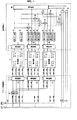
即ち、図6は、第1階層メモリ2の記憶容量を少ないものにした場合において、第1階層の画像を読み出すときの、図1の記憶装置の構成例を示している。
【0125】
この場合、アドレス供給回路1は、遅延回路31および選択回路32乃至34で構成される。遅延回路31には、水平アドレスHAおよび垂直アドレスVAが入力され、そこでは、例えば、そのうちの垂直アドレスVAの上位7ビットva2乃至va8が、その下位3ビット目va2の変化に対応してラッチされて出力されるようになされている。
【0126】
即ち、遅延回路31は、垂直アドレスVAの下位3ビット目va2が0から1に変化するときと、1から0に変化するときとを検出し、その変化の直前の垂直アドレスVAの上位7ビットva2乃至va8をラッチして、残りの垂直アドレスおよび水平アドレスとともに出力するようになされている。従って、遅延回路31が出力する水平アドレスHAおよび垂直アドレスVAは、アドレス供給回路1に供給される水平アドレスHAおよび垂直アドレスVAを4(=23-1)ライン分だけ遅延したものとなる。なお、遅延回路31では、垂直アドレスVAの下位3ビット目va2が変化するときの、その変化直前の垂直アドレスVAの上位7ビットva2乃至va8をラッチすれば良いから、従来における画像をラインディレイするための遅延回路のように、大型のものにはならない。即ち、遅延回路31は、垂直アドレスVAの上位7ビットva2乃至va8をラッチする、例えば、7個のフリップフロップなどで構成することができ、従って、小型に構成することができる。
【0127】
ここで、以下、適宜、遅延回路31が発生する4ライン前の水平アドレスHAまたは垂直アドレスVAを、それぞれ遅延水平アドレスHAまたは遅延垂直アドレス(所定のアドレス信号)という。
【0128】
遅延水平アドレスHAおよび遅延垂直アドレスVAは、選択回路32に供給される。また、遅延水平アドレスHAおよび遅延垂直アドレスVAのうちの、遅延水平アドレスHAの最下位ビットha0を除く上位8ビットha1乃至ha8、および遅延垂直アドレスVAの最下位ビットva0を除く上位8ビットva1乃至va8は、選択回路33に供給される。さらに、遅延水平アドレスHAおよび遅延垂直アドレスVAのうちの、遅延水平アドレスHAの下位2ビットha0,ha1を除く上位7ビットha2乃至ha8、および遅延垂直アドレスVAの下位2ビットva0,va1を除く上位7ビットva2乃至va8は、選択回路34に供給される。
【0129】
選択回路32には、遅延水平アドレスHAおよび遅延垂直アドレスVAの他、アドレス供給回路1に供給される水平アドレスHAおよび垂直アドレスVAがそのまま供給されるとともに、垂直アドレスVAのうちの下位3ビット目va2が、制御信号として供給されるようになされている。そして、選択回路32では、制御信号va2に対応して、遅延水平アドレスHAおよび遅延垂直アドレスVAと、水平アドレスHAおよび垂直アドレスVAのうちの一方がAバンクアドレスとして、他方がBバンクアドレスとして、それぞれ選択され、第1階層メモリ2のAバンクアドレス端子と、Bバンクアドレス端子にそれぞれ供給されるようになされている。
【0130】
即ち、選択回路32は、例えば、遅延水平アドレスHAおよび遅延垂直アドレスVAをAバンクアドレスとして、水平アドレスHAおよび垂直アドレスVAをBバンクアドレスとして、それぞれ選択している場合において、制御信号va2が変化すると、遅延水平アドレスHAおよび遅延垂直アドレスVAをBバンクアドレスとして、水平アドレスHAおよび垂直アドレスVAをAバンクアドレスとして、それぞれ選択する。さらに、その後、選択回路32は、制御信号va2が再度変化すると、遅延水平アドレスHAおよび遅延垂直アドレスVAをAバンクアドレスとして、水平アドレスHAおよび垂直アドレスVAをBバンクアドレスとして、それぞれ再び選択する。従って、選択回路32では、制御信号va2が変化するごとに、遅延水平アドレスHAおよび遅延垂直アドレスVAが、AバンクアドレスまたはBバンクアドレスとして交互に選択されるとともに、水平アドレスHAおよび垂直アドレスVAが、BバンクアドレスまたはAバンクアドレスとして交互に選択される。
【0131】
選択回路33には、遅延水平アドレスHAの上位8ビットha1乃至ha8および遅延垂直アドレスVAの上位8ビットva1乃至va8の他、アドレス供給回路1に供給される水平アドレスHAの上位8ビットha1乃至ha8および垂直アドレスVAの上位8ビットva1乃至va8が供給されるとともに、垂直アドレスVAのうちの下位3ビット目va2が、制御信号として供給されるようになされている。そして、選択回路33においても、選択回路32における場合と同様に、制御信号va2が変化するごとに、遅延水平アドレスHAの上位8ビットha1乃至ha8および遅延垂直アドレスVAの上位8ビットva1乃至va8が、AバンクアドレスまたはBバンクアドレスとして交互に選択されるとともに、水平アドレスHAの上位8ビットha1乃至ha8および垂直アドレスVAの上位8ビットva1乃至va8が、BバンクアドレスまたはAバンクアドレスとして交互に選択されるようになされている。
【0132】
選択回路33において、AバンクアドレスまたはBバンクアドレスとして選択されたものは、第2階層メモリ3のAバンクアドレス端子またはBバンクアドレス端子にそれぞれ供給されるようになされている。
【0133】
選択回路34には、遅延水平アドレスHAの上位7ビットha2乃至ha8および遅延垂直アドレスVAの上位7ビットva2乃至va8の他、アドレス供給回路1に供給される水平アドレスHAの上位7ビットha2乃至ha8および垂直アドレスVAの上位7ビットva2乃至va8が供給されるとともに、垂直アドレスVAのうちの下位3ビット目va2が、制御信号として供給されるようになされている。そして、選択回路34においても、選択回路32における場合と同様に、制御信号va2が変化するごとに、遅延水平アドレスHAの上位7ビットha2乃至ha8および遅延垂直アドレスVAの上位7ビットva2乃至va8が、AバンクアドレスまたはBバンクアドレスとして交互に選択されるとともに、水平アドレスHAの上位7ビットha2乃至ha8および垂直アドレスVAの上位7ビットva2乃至va8が、BバンクアドレスまたはAバンクアドレスとして交互に選択されるようになされている。
【0134】
選択回路34において、AバンクアドレスまたはBバンクアドレスとして選択されたものは、第3階層メモリ4のAバンクアドレス端子またはBバンクアドレス端子にそれぞれ供給されるようになされている。
【0135】
図6の実施の形態においては(後述する図8においても同様)、第1階層メモリ2のアドレス空間は、AバンクとBバンクの2つのバンク(ブロック)に分割されている。即ち、ここでは、図2において、例えば、第8αライン乃至第8α+3ラインの画素を記憶するための第1階層メモリ2の記憶領域がAバンクと、第8α+4ライン乃至第8α+7ラインの画素を記憶するための第1階層メモリ2の記憶領域がBバンクと、それぞれされている(但し、α=0,1,2,・・・,63)。
【0136】
そして、AバンクとBバンクの両方に同時にアクセスが可能なように、Aバンクにアクセスするためのアドレス端子(Aバンクアドレス端子)と、Bバンクにアクセスするためのアドレス端子(Bバンクアドレス端子)の2つのアドレス端子が設けられている。さらに、Aバンク、Bバンクそれぞれに対してデータを読み書きするための入出力端子であるデータ端子も、Aバンクデータ端子およびBバンクデータ端子の2つが設けられている。
【0137】
従って、第1階層メモリ2では、Aバンクアドレス端子に入力されたアドレス(Aバンクアドレス)に対して、Aバンクデータ端子を介して、データ(Aバンクデータ)の読み書きを行うとともに、Bバンクアドレス端子に入力されたアドレス(Bバンクアドレス)に対して、Bバンクデータ端子を介して、データ(Bバンクデータ)の読み書きを行うことができる。
【0138】
ここで、本実施の形態では、遅延水平アドレスHAおよび遅延垂直アドレスVAは、水平アドレスHAおよび垂直アドレスVAを4ライン分(第1段階の画像の4ライン分)遅延したものとなっている。従って、選択回路32において、例えば、水平アドレスHAおよび垂直アドレスVAがAバンクアドレスとして、遅延水平アドレスHAおよび遅延垂直アドレスVAがBバンクアドレスとして、それぞれ選択されている場合、第1階層メモリ2においては、水平アドレスHAおよび垂直アドレスVAに対応するAバンクのメモリセルにアクセスがなされるが、このとき、同時に、その4ライン分の時間だけ前にアクセスされた、遅延水平アドレスHAおよび遅延垂直アドレスVAに対応するBバンクのメモリセルにもアクセスがなされる。
【0139】
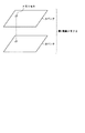
即ち、例えば、図7に示すように、第1階層メモリ2を、Aバンクとしての記憶領域と、Bバンクとしての記憶領域とに分けて考えれば、Aバンクのあるメモリセルにアクセスがなされているとき、同時に、そのメモリセルに対応するBバンクのメモリセルにもアクセスがなされる。この同時にアクセスされるAバンクおよびBバンクの、対応するメモリセルが、本実施の形態では、4ラインに相当する分だけ離れている。ここで、このように同時にアクセスされるAバンクおよびBバンクのメモリセルを、4ラインに相当する分だけ離したのは、本実施の形態では、最上位階層である第3階層の1つの画素が、第1階層の4×4画素を単位として生成されるため、バンクは、少なくとも、そのような単位とするのが好ましいからである。従って、ここでは、4ラインごとに、交互に、AバンクとBバンクとに分けたが、その他、例えば、4列ごとに分けることも可能であるし、バンク数も、AバンクおよびBバンクの2つに限定されるものではない。さらに、横および縦方向の両方向に、即ち、いわば格子状に、バンクをきることも可能である。
【0140】
図6に戻り、第2階層メモリ3においても、第1階層メモリ2と同様に、そのアドレス空間がAバンクとBバンクの2つのバンクに分割されている。但し、本実施の形態では、第2階層の画像を構成する横または縦の画素数それぞれは、第1階層の画像の1/2であるから、第2階層メモリ3においては、第2階層の第4αラインおよび第4α+1ラインの画素を記憶するための第2階層メモリ3の記憶領域がAバンクと、第4α+2ラインおよび第4α+3ラインの画素を記憶するための第2階層メモリ3の記憶領域がBバンクと、それぞれされている。
【0141】
第3階層メモリ4においても、第1階層メモリ2と同様に、そのアドレス空間がAバンクとBバンクの2つのバンクに分割されている。但し、本実施の形態では、第3階層の画像を構成する横または縦の画素数それぞれは、第1階層の画像の1/4であるから、第3階層メモリ4においては、第3階層の第2αラインの画素を記憶するための第3階層メモリ4の記憶領域がAバンクと、第2α+1ラインの画素を記憶するための第3階層メモリ4の記憶領域がBバンクと、それぞれされている。
【0142】
第1階層メモリ2のAバンクまたはBバンクそれぞれから読み出されたデータ(AバンクデータまたはBバンクデータ)が出力されるAバンクデータ端子またはBバンクデータ端子は、いずれも選択回路41に接続されている。また、選択回路41には、アドレス供給回路1から、垂直アドレスVAの下位3ビット目va2が、制御信号として供給されるようになされており、選択回路41では、制御信号va2に対応して、Aバンクデータ端子またはBバンクデータ端子のうちの一方が読み出し部44に接続され、他方が読み出し部45に接続されるようになされている。
【0143】
即ち、選択回路41は、ある時点において、例えば、Aバンクデータ端子またはBバンクデータ端子を、読み出し部44または45にそれぞれ接続している場合において、制御信号va2が変化すると、Aバンクデータ端子またはBバンクデータ端子を、読み出し部45または44にそれぞれ接続する。さらに、その後、制御信号va2が再度変化すると、選択回路41は、Aバンクデータ端子またはBバンクデータ端子を、読み出し部44または45にそれぞれ再び接続する。従って、選択回路41によれば、制御信号va2が変化するごとに、Aバンクデータ端子が読み出し部44または45に交互に接続されるとともに、Bバンクデータ端子が読み出し部45または44に交互に接続される。
【0144】
第2階層メモリ3のAバンクに書き込まれるデータが供給されるとともに、Aバンクから読み出されたデータが出力されるAバンクデータ端子、およびそのBバンクに書き込まれるデータが供給されるとともに、Bバンクから読み出されたデータが出力されるBバンクデータ端子は、いずれも選択回路42に接続されている。また、選択回路42にも、アドレス供給回路1から、垂直アドレスVAの下位3ビット目va2が、制御信号として供給されるようになされており、選択回路42では、制御信号va2に対応して、Aバンクデータ端子またはBバンクデータ端子のうちの一方が書き込み部46および読み出し部47に接続され、他方が書き込み部48および読み出し部49に接続されるようになされている。
【0145】
即ち、選択回路42は、ある時点において、例えば、Aバンクデータ端子を書き込み部46および読み出し部47に接続し、Bバンクデータ端子を書き込み部48および読み出し部49に接続している場合において、制御信号va2が変化すると、Aバンクデータ端子を書き込み部48および読み出し部49に接続し、Bバンク端子を書き込み部46および読み出し部47に接続する。さらに、その後、制御信号va2が再度変化すると、選択回路42は、Aバンクデータ端子を書き込み部46および読み出し部47に再び接続するとともに、Bバンクデータ端子を書き込み部48および読み出し部49に再び接続する。従って、選択回路42によれば、制御信号va2が変化するごとに、Aバンクデータ端子が、書き込み部46と読み出し部47、または書き込み部48と読み出し部49に交互に接続されるとともに、Bバンクデータ端子が、書き込み部48と読み出し部49、または書き込み部46と読み出し部47に交互に接続される。
【0146】
第3階層メモリ4のAバンクに書き込まれるデータが供給されるとともに、Aバンクから読み出されたデータが出力されるAバンクデータ端子、およびそのBバンクに書き込まれるデータが供給されるとともに、Bバンクから読み出されたデータが出力されるBバンクデータ端子は、いずれも選択回路43に接続されている。また、選択回路43にも、アドレス供給回路1から、垂直アドレスVAの下位3ビット目va2が、制御信号として供給されるようになされている。そして、選択回路43においても、選択回路42における場合と同様に、制御信号va2が変化するごとに、Aバンクデータ端子が、書き込み部50と読み出し部51、または書き込み部52と読み出し部53に交互に接続されるとともに、Bバンクデータ端子が、書き込み部52と読み出し部53、または書き込み部50と読み出し部51に交互に接続されるようになされている。
【0147】
読み出し部44または45は、選択回路41を介して、第1階層メモリ2からデータを読み出すようになされている。読み出し部44が読み出したデータは、演算器54および選択回路58に供給されるとともに、スイッチ61を介して演算器56に供給されるようになされている。また、読み出し部45が読み出したデータは、演算器55および57に供給されるようになされている。書き込み部46は、演算器54の出力を、選択回路42を介して、第2階層メモリ3に書き込むようになされている。読み出し部47は、選択回路42を介して、第2階層メモリ3からデータを読み出し、演算器54および選択回路58に供給するようになされている。書き込み部48は、演算器55の出力を、選択回路42を介して、第2階層メモリ3に書き込むようになされている。読み出し部49は、選択回路42を介して、第2階層メモリ3からデータを読み出し、演算器55およびスイッチ62に供給するようになされている。書き込み部50は、演算器56の出力を、選択回路43を介して、第3階層メモリ4に書き込むようになされている。読み出し部51は、選択回路43を介して、第3階層メモリ4からデータを読み出し、演算器56および選択回路58に供給するようになされている。書き込み部52は、演算器57の出力を、選択回路43を介して、第3階層メモリ4に書き込むようになされている。読み出し部53は、選択回路43を介して、第3階層メモリ4からデータを読み出し、演算器57に供給するようになされている。
【0148】
演算器54は、読み出し部47の出力から、読み出し部44の出力を減算して、その減算結果を、書き込み部46に供給するようになされている。演算器55は、読み出し部45および49の出力どうしを加算し、その加算結果を、書き込み部48に供給するようになされている。演算器56は、読み出し部51の出力から、スイッチ61を介して供給される信号を減算し、書き込み部50に供給するようになされている。演算器57は、読み出し部45および53の出力どうしを加算し、その加算結果を、書き込み部52に供給するようになされている。なお、演算器57は、スイッチ62がオン状態になっており、これにより、読み出し部49の出力が供給される場合は、その出力も加算の対象とするようになされている。
【0149】
選択回路58は、ANDゲート59および60の出力に対応して、読み出し部44,47、または51の出力のうちのいずれかを選択して出力するようになされている。ANDゲート59には、アドレス供給回路1から、水平アドレスHAの最下位ビットha0と、垂直アドレスVAの最下位ビットva0が、制御信号として供給されるようになされており、ANDゲート59は、その論理積を演算して、選択回路58に供給するようになされている。ANDゲート60には、アドレス供給回路1から、水平アドレスHAの下位2ビット目ha1と、垂直アドレスVAの下位2ビット目va1が、制御信号として供給されるようになされており、ANDゲート60は、その論理積を演算して、選択回路58に供給するようになされている。
【0150】
スイッチ61は、ANDゲート59の出力に対応して、端子61aまたは61bのうちのいずれか一方を選択するようになされている。なお、端子61aまたは61bには、読み出し部44または47の出力がそれぞれ供給されるようになされている。スイッチ62は、NORゲート63の出力に対応してオン/オフし、読み出し部49の出力を、演算器57に供給するようになされている。NORゲート63には、ANDゲート59と同様に、最下位ビットha0とva0が供給されるようになされており、その出力によって、スイッチ62のオン/オフが制御されるようになされている。
【0151】
ここでは、以上の選択回路41乃至43、読み出し部44,45、書き込み部46、読み出し部47、書き込み部48、読み出し部49、書き込み部50、読み出し部51、書き込み部52、読み出し部53、演算器54乃至57、選択回路58、ANDゲート59,60、スイッチ61,62、およびNORゲート63で、RMW回路5が構成されている。
【0152】
なお、図6(後述する図8においても同様)においては、クロック、R/W信号、および階層フラグの図示は省略してある。
【0153】
次に、その動作について説明する。
【0154】
いま、選択回路32において、例えば、アドレス供給回路1に供給された水平アドレスHAおよび垂直アドレスVAがAバンクアドレスとして、遅延水平アドレスHAおよび遅延垂直アドレスVAがBバンクアドレスとして、それぞれ選択されているとする。
【0155】
この場合、選択回路33および34においても、同様にして、AバンクアドレスおよびBバンクアドレスが選択される。即ち、選択回路33では、水平アドレスHAの上位8ビットha1乃至ha8および垂直アドレスVAの上位8ビットva1乃至va8が、Aバンクアドレスとして、遅延水平アドレスHAの上位8ビットha1乃至ha8および遅延垂直アドレスVAの上位8ビットva1乃至va8が、Bバンクアドレスとして、それぞれ選択される。また、選択回路34では、水平アドレスHAの上位7ビットha2乃至ha8および垂直アドレスVAの上位7ビットva2乃至va8が、Aバンクアドレスとして、遅延水平アドレスHAの上位7ビットha2乃至ha8および遅延垂直アドレスVAの上位7ビットva2乃至va8が、Bバンクアドレスとして、それぞれ選択される。
【0156】
選択回路32乃至34において選択されたAバンクアドレスとBバンクアドレスは、第1階層メモリ2、第2階層メモリ3、または第3階層メモリ4それぞれのAバンクアドレス端子とBバンクアドレス端子に供給される。
【0157】
さらに、この場合、選択回路41においては、第1階層メモリ2のAバンクデータ端子が読み出し部44に接続されるとともに、そのBバンクデータ端子が読み出し部45に接続される。また、選択回路42では、第2階層メモリ3のAバンクデータ端子が、書き込み部46および読み出し部47に接続されるとともに、そのBバンクデータ端子が、書き込み部48および読み出し部49に接続される。さらに、選択回路43では、第3階層メモリ4のAバンクデータ端子が、書き込み部50および読み出し部51に接続されるとともに、そのBバンクデータ端子が、書き込み部52および読み出し部53に接続される。
【0158】
読み出し部44は、第1階層メモリ2から、選択回路32が出力するAバンクアドレスに記憶されている第1階層の画素(画素値)を、選択回路41を介して読み出し、演算器54、選択回路58、およびスイッチ61の端子61aに供給する。
【0159】
選択回路58は、ANDゲート59の出力が1でないとき(0のとき)、読み出し部44の出力を、第1階層の画素として選択して出力する。即ち、ANDゲート59の出力が1でないときというのは、ha0またはva0のうちの少なくとも一方が0であるときであり、図2にD1で示すような第1階層の2×2の4画素h(2s,2t),h(2s+1,2t),h(2s,2t+1),h(2s+1,2t+1)のうちの、右下の画素h(2s+1,2t+1)を除く画素h(2s,2t),h(2s+1,2t),h(2s,2t+1)の中のいずれかが読み出されるタイミングである。h(2s,2t),h(2s+1,2t),h(2s,2t+1)は、いずれも、第1階層メモリ2に記憶されているから、その第1階層メモリ2から読み出された値が、そのまま、選択部58で選択されて出力される。
【0160】
一方、読み出し部47は、第2階層メモリ3から、選択回路33が出力するAバンクアドレスに記憶されている第2階層の画素(画素値)を、選択回路42を介して読み出し、演算器54、選択回路58、およびスイッチ61の端子61bに供給する。
【0161】
ここで、第1階層の2×2の4画素h(2s,2t),h(2s+1,2t),h(2s,2t+1),h(2s+1,2t+1)にアクセスがなされるタイミングにおいては、即ち、第1階層メモリ2のAバンクアドレス(2s,2t),(2s+1,2t),(2s,2t+1),(2s+1,2t+1)にアクセスがなされる場合においては、上述したことから、いずれの場合においても、第2階層メモリ3のAバンクアドレス(s,t)にアクセスがなされる。
【0162】
従って、読み出し部44が、第1階層メモリ2から、第1階層の画素h(2s,2t),h(2s+1,2t),h(2s,2t+1)を読み出し、演算器54に供給するとき、読み出し部47においては、第2階層メモリ3のAバンクアドレス(s,t)からデータが読み出され、演算器54に供給される。
【0163】
演算器54では、読み出し部47の出力から読み出し部44の出力が減算され、書き込み部46に供給される。書き込み部46は、演算器54の出力を、選択回路42を介して、第2階層メモリ3のAバンクアドレス(s,t)に書き込む。
【0164】
従って、最初は、第2階層メモリ3のAバンクアドレス(s,t)には、第1階層の2×2の4画素h(2s,2t),h(2s+1,2t),h(2s,2t+1),h(2s+1,2t+1)の加算値である第2階層の画素m(s,t)が記憶されているが、読み出し部44が、第1階層の画素h(2s,2t)を読み出すとともに、読み出し部47が、第2階層メモリ3のAバンクアドレス(s,t)に記憶されているデータ(ここでは、m(s,t))を読み出すことで、演算器54において、それらの減算値(m(s,t)−h(2s,2t))が求められ、書き込み部46において、第2階層メモリ3のAバンクアドレス(s,t)に書き込まれる。
【0165】
さらに、読み出し部44が、第1階層の画素h(2s+1,2t)を読み出すとともに、読み出し部47が、第2階層メモリ3のAバンクアドレス(s,t)に記憶されているデータ(ここでは、m(s,t)−h(2s,2t))を読み出すことで、演算器54において、それらの減算値(m(s,t)−h(2s,2t)−h(2s+1,2t))が求められ、書き込み部46において、第2階層メモリ3のAバンクアドレス(s,t)に書き込まれる。
【0166】
その後、読み出し部44が、第1階層の画素h(2s,2t+1)を読み出すとともに、読み出し部47が、第2階層メモリ3のAバンクアドレス(s,t)に記憶されているデータ(ここでは、m(s,t)−h(2s,2t)−h(2s+1,2t))を読み出すことで、演算器54において、それらの減算値(m(s,t)−h(2s,2t)−h(2s+1,2t)−h(2s,2t+1))が求められ、書き込み部46において、第2階層メモリ3のAバンクアドレス(s,t)に書き込まれる。即ち、第2階層メモリ3のAバンクアドレス(s,t)には、第1階層の画素h(2s+1,2t+1)(=m(s,t)−h(2s,2t)−h(2s+1,2t)−h(2s,2t+1))が書き込まれる。
【0167】
従って、第1階層メモリ2のAバンクアドレス(2s+1,2t+1)(ここでは、このアドレスに対応するメモリセルはなく、従って、このアドレスにアクセスがなされても、例えば、何も書き込まれず、何も読み出されない)にアクセスがなされるタイミングにおいては、読み出し部47が、第2階層メモリ3のAバンクアドレス(s,t)から読み出すデータは、図2にD1で示すような第1階層の2×2の4画素h(2s,2t),h(2s+1,2t),h(2s,2t+1),h(2s+1,2t+1)のうちの、右下の画素(画素値)h(2s+1,2t+1)(但し、h(4m+3,4n+3)を除く)になっている。
【0168】
一方、選択回路58は、ANDゲート59または60の出力のうちの、ANDゲート59の出力のみが1のとき(従って、ANDゲート60の出力は0)、読み出し部47の出力を、第1階層の画素として選択して出力する。即ち、ANDゲート59の出力のみが1のときというのは、ha0およびva0の両方が1で、ha1またはva1のうちのいずれか一方、または両方が0であるときであり、図2にD1で示すような第1階層の2×2の4画素h(2s,2t),h(2s+1,2t),h(2s,2t+1),h(2s+1,2t+1)のうちの、右下の画素h(2s+1,2t+1)(但し、h(4m+3,4n+3)を除く)が読み出されるタイミングである。この画素h(2s+1,2t+1)は、上述したように、第2階層メモリ3のAバンクアドレス(s,t)から、読み出し部47によって読み出されるから、読み出し部47の出力が、選択部58で選択されて出力される。
【0169】
一方、読み出し部51は、第3階層メモリ4から、選択回路34が出力するAバンクアドレスに記憶されている第3階層の画素(画素値)を、選択回路43を介して読み出し、演算器56および選択回路58に供給する。
【0170】
ここで、図2にD2で示すような第1階層の4×4の16画素h(4m,4n),h(4m+1,4n),h(4m+2,4n),h(4m+3,4n),h(4m,4n+1),h(4m+1,4n+1),h(4m+2,4n+1),h(4m+3,4n+1),h(4m,4n+2),h(4m+1,4n+2),h(4m+2,4n+2),h(4m+3,4n+2),h(4m,4n+3),h(4m+1,4n+3),h(4m+2,4n+3),h(4m+3,4n+3)にアクセスがなされるタイミングでは、上述したことから、いずれの場合においても、第3階層メモリ4のAバンクアドレス(m,n)にアクセスがなされる。
【0171】
従って、読み出し部44が、第1階層メモリ2から、第1階層の2×2画素のうちの右下の画素h(2s+1,2t+1)を除く第1階層の画素h(4m,4n),h(4m+1,4n),h(4m+2,4n),h(4m+3,4n),h(4m,4n+1),h(4m+2,4n+1),h(4m,4n+2),h(4m+1,4n+2),h(4m+2,4n+2),h(4m+3,4n+2),h(4m,4n+3),h(4m+2,4n+3)を読み出し、端子61aに供給するとき、読み出し部51においては、第3階層メモリ4のAバンクアドレス(m,n)からデータが読み出され、演算器56に供給される。
【0172】
スイッチ61は、ANDゲート59の出力が0のとき、端子61aを選択するようになされており、従って、読み出し部44が出力する第1階層の画素h(4m,4n),h(4m+1,4n),h(4m+2,4n),h(4m+3,4n),h(4m,4n+1),h(4m+2,4n+1),h(4m,4n+2),h(4m+1,4n+2),h(4m+2,4n+2),h(4m+3,4n+2),h(4m,4n+3),h(4m+2,4n+3)は、スイッチ61を介して演算器56に供給される。
【0173】
また、読み出し部47が、上述したようにして、第1階層の2×2画素の右下の画素h(2s+1,2t+1)に相当する画素h(4m+1,4n+1),h(4m+3,4n+1),h(4m+1,4n+3)を出力するとき、即ち、ANDゲート59の出力が1のとき、スイッチ61は、端子61bを選択するようになされており、従って、読み出し部47が出力する第1階層の画素h(4m+1,4n+1),h(4m+3,4n+1),h(4m+1,4n+3)も、スイッチ61を介して演算器56に供給される。
【0174】
演算器56では、読み出し部51の出力からスイッチ61の出力が減算され、書き込み部50に供給される。書き込み部50は、演算器56の出力を、選択回路43を介して、第3階層メモリ4のAバンクアドレス(m,n)に書き込む。
【0175】
従って、最初は、第3階層メモリ4のAバンクアドレス(m,n)には、第1階層の、上述の4×4の16画素の加算値である第3階層の画素q(m,n)が記憶されているが、読み出し部44が、第1階層の画素h(4m,4n)を読み出すとともに、読み出し部51が、第3階層メモリ4のAバンクアドレス(m,n)に記憶されているデータ(ここでは、q(m,n))を読み出すことで、演算器56において、それらの減算値(q(m,n)−h(4m,4n))が求められ、書き込み部50において、第3階層メモリ4のAバンクアドレス(m,n)に書き込まれる。
【0176】
さらに、読み出し部44が、第1階層の画素h(4m+1,4n)を読み出すとともに、読み出し部51が、第3階層メモリ4のAバンクアドレス(m,n)に記憶されているデータ(ここでは、q(m,n)−h(4m,4n))を読み出すことで、演算器56において、それらの減算値(q(m,n)−h(4m,4n)−h(4m+1,4n))が求められ、書き込み部50において、第3階層メモリ4のAバンクアドレス(m,n)に書き込まれる。
【0177】
以下、同様にして、第3階層メモリ4のAバンクアドレス(m,n)の記憶値が書き換えられていく。
【0178】
そして、読み出し部47において、第1階層の2×2画素のうちの右下の画素h(2s+1,2t+1)に相当する第1階層の画素h(4m+1,4n+1)が読み出されると、これは、上述したように、スイッチ61を介して、演算器56に供給される。このとき、第3階層メモリ4のAバンクアドレス(m,n)には、式q(m,n)−h(4m,4n)−h(4m+1,4n)−h(4m+2,4n)−h(4m+3,4n)−h(4m,4n+1)で表されるデータが記憶されており、読み出し部51では、このデータが読み出され、演算器56に供給される。
【0179】
演算器56では、読み出し部51の出力から読み出し部47の出力が減算され、その減算値(q(m,n)−h(4m,4n)−h(4m+1,4n)−h(4m+2,4n)−h(4m+3,4n)−h(4m,4n+1)−h(4m+1,4n+1))が、書き込み部50によって、第3階層メモリ4のAバンクアドレス(m,n)に書き込まれる。
【0180】
以下、同様にして、最終的には、即ち、読み出し部44が、第1階層の画素h(4m+2,4n+3)を読み出すとともに、読み出し部51が、第3階層メモリ4のAバンクアドレス(m,n)に記憶されているデータ(ここでは、q(m,n)−h(4m,4n)−h(4m+1,4n)−h(4m+2,4n)−h(4m+3,4n)−h(4m,4n+1)−h(4m+1,4n+1)−h(4m+2,4n+1)−h(4m+3,4n+1)−h(4m,4n+2)−h(4m+1,4n+2)−h(4m+2,4n+2)−h(4m+3,4n+2)−h(4m,4n+3)−h(4m+1,4n+3))を読み出すことで、演算器56において、それらの減算値が求められ、書き込み部50において、第3階層メモリ4のAバンクアドレス(m,n)に書き込まれる。即ち、第3階層メモリ4のAバンクアドレス(m,n)には、第1階層の画素h(4m+3,4n+3)(=q(m,n)−h(4m,4n)−h(4m+1,4n)−h(4m+2,4n)−h(4m+3,4n)−h(4m,4n+1)−h(4m+1,4n+1)−h(4m+2,4n+1)−h(4m+3,4n+1)−h(4m,4n+2)−h(4m+1,4n+2)−h(4m+2,4n+2)−h(4m+3,4n+2)−h(4m,4n+3)−h(4m+1,4n+3)−h(4m+2,4n+3))が書き込まれる。
【0181】
従って、第1階層メモリ2のAバンクアドレス(4m+3,4n+3)(ここでは、このアドレスに対応するメモリセルはなく、従って、このアドレスにアクセスがなされても、例えば、何も書き込まれず、何も読み出されない)にアクセスがなされるタイミングにおいては、読み出し部51が、第3階層メモリ4のAバンクアドレス(m,n)から読み出すデータは、図2にD2で示すような第1階層の4×4の16画素のうちの、右下の画素(画素値)h(4m+3,4n+3)になっている。
【0182】
一方、選択回路58は、ANDゲート59および60の両方の出力が1のとき、読み出し部51の出力を、第1階層の画素として選択して出力する。即ち、ANDゲート59および50の両方の出力が1のときというのは、ha0,va0,ha1,va1のすべてが1であるときであり、図2にD2で示すような第1階層の4×4の16画素のうちの、右下の画素h(4m+3,4n+3)が読み出されるタイミングである。この画素h(4m+3,4n+3)は、上述したように、第3階層メモリ4のAバンクアドレス(m,n)から、読み出し部51によって読み出されるから、読み出し部51の出力が、選択部58で選択されて出力される。
【0183】
ところで、以上のようにして、第1階層の画素が読み出されていくと、第2階層メモリ3には、第1階層の画素h(2s+1,2t+1)(但し、h(4m+3,4n+3)を除く)が記憶されるようになり、また、第3階層メモリ4には、第1階層の画素h(4m+3,4n+3)が記憶されるようになる。
【0184】
即ち、第2階層メモリ3または第3階層メモリ4の記憶値は、第2または第3階層の画素それぞれから、第1階層の画素に書き換えられる。
【0185】
従って、このように書き換えられた第2階層メモリ3または第3階層メモリ4の記憶値を、それぞれ、元の第2または第3階層の画素に戻す必要がある(但し、必要がなければ、戻さなくてもよい)。
【0186】
そこで、上述したように、第1階層メモリ2は、第8αライン乃至第8α+3ラインの画素を記憶するためのAバンクと、第8α+4ライン乃至第8α+7ラインの画素を記憶するためのBバンクとに分離されている。さらに、第2階層メモリ3は、第2階層の第4αラインおよび第4α+1ラインの画素を記憶するためのAバンクと、第2階層の第4α+2ラインおよび第4α+3ラインの画素を記憶するためのBバンクとに分離されており、また、第3階層メモリ4は、第3階層の第2αラインの画素を記憶するためのAバンクと、第2α+1ラインの画素を記憶するためのBバンクとに分離されている。
【0187】
そして、本実施の形態では、遅延水平アドレスHAおよび遅延垂直アドレスVAは、水平アドレスHAおよび垂直アドレスVAを4ライン分遅延したものとなっており、上述したように、水平アドレスHAおよび垂直アドレスVAがAバンクアドレスとして、遅延水平アドレスHAおよび遅延垂直アドレスVAがBバンクアドレスとして、それぞれ選択されている場合には、第1階層メモリ2においては、水平アドレスHAおよび垂直アドレスVAに対応するAバンクのメモリセルにアクセスがなされるが、このとき、同時に、その4ライン分だけ前にアクセスされた、遅延水平アドレスHAおよび遅延垂直アドレスVAに対応するBバンクのメモリセル(Aバンクのメモリセルの位置に対応するBバンクのメモリセル)にもアクセスがなされる。
【0188】
同様に、第2階層メモリ3においては、Aバンクのメモリセルにアクセスがなされるとともに、2ライン分だけ前にアクセスされたBバンクのメモリセルにアクセスがなされる。さらに、第3階層メモリ4においては、Aバンクのメモリセルにアクセスがなされるとともに、1ライン分だけ前にアクセスされたBバンクのメモリセルにアクセスがなされる。
【0189】
従って、読み出し部44が、第1階層メモリ2のAバンクから、第1階層の画素h(2s,2t),h(2s+1,2t),h(2s,2t+1)を読み出すとき、読み出し部45においては、選択回路41を介して、第1階層メモリ2のBバンクから、4ライン前にアクセスされた第1階層の画素h(2s,2t’),h(2s+1,2t’),h(2s,2t’+1)がそれぞれ読み出され、演算器55に供給される。ここで、t’=t−2である。
【0190】
また、読み出し部45が、第1階層メモリ2のBバンクから、第1階層の画素h(2s,2t’),h(2s+1,2t’),h(2s,2t’+1)を読み出すとき、読み出し部49においては、いずれのときも、選択回路42を介して、第2階層メモリ3のBバンクにおけるアドレス(所定のアドレス)(s,t’)から、データが読み出され、演算器55に供給される。
【0191】
演算器55では、読み出し部45の出力と読み出し部49の出力とが加算され、その加算値は、書き込み部48に供給される。書き込み部48は、演算器55の出力を、選択回路42を介して、第2階層メモリ3のBバンクアドレス(s,t’)に書き込む。
【0192】
従って、最初は、第2階層メモリ3のBバンクアドレス(s,t’)には、第2階層について2ライン分(第1階層については4ライン分)だけ前にアクセスされることによって求められた第1階層の画素h(2s+1,2t’+1)が記憶されているが、読み出し部45が、第1階層メモリ2のBバンクから、第1階層の画素h(2s,2t’)を読み出すとともに、読み出し部49が、第2階層メモリ3のBバンクアドレス(s,t’)に記憶されているデータ(ここでは、h(2s+1,2t’+1))を読み出すことで、演算器55において、それらの加算値(h(2s,2t’)+h(2s+1,2t’+1))が求められ、書き込み部48において、第2階層メモリ3のBバンクアドレス(s,t’)に書き込まれる。
【0193】
さらに、読み出し部45が、第1階層メモリ2のBバンクから、第1階層の画素h(2s+1,2t’)を読み出すとともに、読み出し部49が、第2階層メモリ3のBバンクアドレス(s,t’)に記憶されているデータ(ここでは、h(2s,2t’)+h(2s+1,2t’+1))を読み出すことで、演算器55において、それらの加算値(h(2s,2t’)+h(2s+1,2t)+h(2s+1,2t’+1))が求められ、書き込み部48において、第2階層メモリ3のBバンクアドレス(s,t’)に書き込まれる。
【0194】
その後、読み出し部45が、第1階層メモリ2のBバンクから、第1階層の画素h(2s,2t’+1)を読み出すとともに、読み出し部49が、第2階層メモリ3のBバンクアドレス(s,t’)に記憶されているデータ(ここでは、h(2s,2t’)+h(2s+1,2t)+h(2s+1,2t’+1))を読み出すことで、演算器55において、それらの加算値(h(2s,2t’)+h(2s+1,2t)+h(2s,2t’+1)+h(2s+1,2t’+1))が求められ、書き込み部48において、第2階層メモリ3のBバンクアドレス(s,t’)に書き込まれる。即ち、第2階層メモリ3のBバンクアドレス(s,t’)には、元の第2階層の画素m(s,t’)(=h(2s,2t’)+h(2s+1,2t)+h(2s,2t’+1)+h(2s+1,2t’+1))が書き込まれる。
【0195】
また、読み出し部44が、第1階層メモリ2のAバンクから、第1階層の2×2画素のうちの右下の画素h(2s+1,2t+1)を除く第1階層の画素h(4m,4n),h(4m+1,4n),h(4m+2,4n),h(4m+3,4n),h(4m,4n+1),h(4m+2,4n+1),h(4m,4n+2),h(4m+1,4n+2),h(4m+2,4n+2),h(4m+3,4n+2),h(4m,4n+3),h(4m+2,4n+3)を読み出すとき、読み出し部45においては、第1階層メモリ2のBバンクから、選択回路41を介して、4ライン前の第1階層の画素h(4m,4n’),h(4m+1,4n’),h(4m+2,4n’),h(4m+3,4n’),h(4m,4n’+1),h(4m+2,4n’+1),h(4m,4n’+2),h(4m+1,4n’+2),h(4m+2,4n’+2),h(4m+3,4n’+2),h(4m,4n’+3),h(4m+2,4n’+3)がそれぞれ読み出され、演算器57に供給される。但し、n’=n−1である。
【0196】
さらに、この場合、読み出し部53においては、選択回路43を介して、第3階層メモリ4のBバンクアドレス(m,n’)からデータが読み出され、演算器57に供給される。
【0197】
演算器57には、さらに、スイッチ62を介して、読み出し部49の出力も供給されるようになされている。スイッチ62は、NORゲート63の出力がHレベルの場合(ha0=va0=0の場合)のみオンし、他の場合はオフするようになされている。従って、スイッチ62は、読み出し部49が、第2階層メモリ3のBバンクから、第1階層の画素h(4m+1,4n’+1),h(4m+3,4n’+1),h(4m+1,4n’+3)を読み出すときのみオンし、その結果、その第1階層の画素h(4m+1,4n’+1),h(4m+3,4n’+1),h(4m+1,4n’+3)は、スイッチ62を介して演算器57に供給される。
【0198】
演算器57では、読み出し部45の出力と読み出し部53の出力とが加算され、さらに、スイッチ62がオンしており、読み出し部49の出力が供給される場合には、その出力も加算され、その加算値は、書き込み部52に供給される。書き込み部52は、演算器57の出力を、選択回路43を介して、第3階層メモリ4のBバンクアドレス(m,n’)に書き込む。
【0199】
従って、最初は、第3階層メモリ4のAバンクアドレス(m,n’)には、第3階層について1ライン分(第1階層については4ライン分)だけ前にアクセスされることによって求められた第1階層の画素h(4m+3,4n’+3)が記憶されているが、読み出し部45または49が、第1階層の画素h(4m,4n’)またはh(4m+1,4n’+1)をそれぞれ読み出すとともに、読み出し部53が、第3階層メモリ4のBバンクアドレス(m,n’)に記憶されているデータ(ここでは、h(4m+3,4n’+3))を読み出すことで、演算器57において、それらの加算値(h(4m,4n’)+h(4m+1,4n’+1)+h(4m+3,4n’+3))が求められ、書き込み部52において、第3階層メモリ4のBバンクアドレス(m,n’)に書き込まれる。
【0200】
さらに、読み出し部45が、第1階層の画素h(4m+1,4n’)を読み出すとともに、読み出し部53が、第3階層メモリ4のBバンクアドレス(m,n’)に記憶されているデータ(ここでは、h(4m,4n’)+h(4m+1,4n’+1)+h(4m+3,4n’+3))を読み出すことで、演算器57において、それらの加算値(h(4m,4n’)+h(4m+1,4n’)+h(4m+1,4n’+1)+h(4m+3,4n’+3))が求められ、書き込み部52において、第3階層メモリ4のBバンクアドレス(m,n’)に書き込まれる。
【0201】
以下、同様にして、最終的には、即ち、読み出し部45が、第1階層の画素h(4m+2,4n’+3)を読み出すとともに、読み出し部53が、第3階層メモリ4のBバンクアドレス(m,n’)に記憶されているデータ(ここでは、h(4m,4n’)+h(4m+1,4n’)+h(4m+2,4n’)+h(4m+3,4n’)+h(4m,4n’+1)+h(4m+1,4n’+1)+h(4m+2,4n’+1)+h(4m+3,4n’+1)+h(4m,4n’+2)+h(4m+1,4n’+2)+h(4m+2,4n’+2)+h(4m+3,4n’+2)+h(4m,4n’+3)+h(4m+1,4n’+3)+h(4m+3,4n’+3))を読み出すことで、演算器57において、それらの加算値が求められ、書き込み部52において、第3階層メモリ4のBバンクアドレス(m,n’)に書き込まれる。即ち、第3階層メモリ4のBバンクアドレス(m,n’)には、元の第3階層の画素q(m,n’)(=h(4m,4n’)+h(4m+1,4n’)+h(4m+2,4n’)+h(4m+3,4n’)+h(4m,4n’+1)+h(4m+1,4n’+1)+h(4m+2,4n’+1)+h(4m+3,4n’+1)+h(4m,4n’+2)+h(4m+1,4n’+2)+h(4m+2,4n’+2)+h(4m+3,4n’+2)+h(4m,4n’+3)+h(4m+1,4n’+3)+h(4m+2,4n’+3)+h(4m+3,4n’+3))が書き込まれる。
【0202】
その後、垂直アドレスVAの下位3ビット目va2が変化すると、選択回路32において、アドレス供給回路1に供給された水平アドレスHAおよび垂直アドレスVAがBバンクアドレスとして、遅延水平アドレスHAおよび遅延垂直アドレスVAがAバンクアドレスとして、それぞれ選択される。
【0203】
この場合、選択回路33および34においても、同様にして、AバンクアドレスおよびBバンクアドレスが選択される。即ち、選択回路33では、水平アドレスHAの上位8ビットha1乃至ha8および垂直アドレスVAの上位8ビットva1乃至va8が、Bバンクアドレスとして、遅延水平アドレスHAの上位8ビットha1乃至ha8および遅延垂直アドレスVAの上位8ビットva1乃至va8が、Aバンクアドレスとして、それぞれ選択される。また、選択回路34では、水平アドレスHAの上位7ビットha2乃至ha8および垂直アドレスVAの上位7ビットva2乃至va8が、Bバンクアドレスとして、遅延水平アドレスHAの上位7ビットha2乃至ha8および遅延垂直アドレスVAの上位7ビットva2乃至va8が、Aバンクアドレスとして、それぞれ選択される。
【0204】
選択回路32乃至34において選択されたAバンクアドレスとBバンクアドレスは、第1階層メモリ2、第2階層メモリ3、または第3階層メモリ4のそれぞれAバンクアドレス端子とBバンクアドレス端子に供給される。
【0205】
さらに、選択回路41においては、第1階層メモリ2のBバンクデータ端子が読み出し部44に接続されるとともに、そのAバンクデータ端子が読み出し部45に接続される。また、選択回路42では、第2階層メモリ3のBバンクデータ端子が、書き込み部46および読み出し部47に接続されるとともに、そのAバンクデータ端子が、書き込み部48および読み出し部49に接続される。さらに、選択回路43では、第3階層メモリ4のBバンクデータ端子が、書き込み部50および読み出し部51に接続されるとともに、そのAバンクデータ端子が、書き込み部52および読み出し部53に接続される。
【0206】
そして、上述の処理におけるAバンクまたはBバンクを、BバンクまたはAバンクとそれぞれ読み替えた処理が行われる。
【0207】
以下、同様の処理が行われ、第1階層の画素が選択回路58から出力されていくとともに、それに伴い書き換えられる第2階層メモリ3および第3階層メモリ4の記憶内容が、元の値に、再度書き換えられる。
【0208】
次に、図8は、第1階層メモリ2および第2階層メモリ3を、上述のように、少ない記憶容量のものとした場合における、第2階層の画像を読み出すときの、図1の記憶装置の構成例を示している。なお、図8においては、第1階層メモリ2に関する部分の図示は省略してある。
【0209】
この場合、アドレス供給回路1は、遅延回路71、並びに選択回路73および74で構成される。遅延回路31、選択回路73,74は、図6における遅延回路31、選択回路33,34とそれぞれ同様に構成されている。
【0210】
また、第2階層メモリ3および第3階層メモリ4も、図6における場合と同様に構成されている。
【0211】
さらに、RMW回路5は、選択回路81,82、読み出し部84,85、書き込み部86、読み出し部87、書き込み部88、読み出し部89、スイッチ91,92、演算器94,95、選択回路98,ANDゲート99,100で構成されている。
【0212】
第2階層メモリ3のAバンクまたはBバンクそれぞれから読み出されたデータ(AバンクデータまたはBバンクデータ)が出力されるAバンクデータ端子またはBバンクデータ端子は、いずれも選択回路81に接続されている。また、選択回路81には、アドレス供給回路1から、垂直アドレスVAの下位3ビット目va2が、制御信号として供給されるようになされており、選択回路81では、制御信号va2に対応して、Aバンクデータ端子またはBバンクデータ端子のうちの一方が読み出し部84に接続され、他方が読み出し部85に接続されるようになされている。
【0213】
即ち、選択回路81は、ある時点において、例えば、Aバンクデータ端子またはBバンクデータ端子を、読み出し部84または85にそれぞれ接続している場合において、制御信号va2が変化すると、Aバンクデータ端子またはBバンクデータ端子を、読み出し部85または84にそれぞれ接続する。さらに、その後、制御信号va2が再度変化すると、選択回路81は、Aバンクデータ端子またはBバンクデータ端子を、読み出し部84または85にそれぞれ再び接続する。従って、選択回路81によれば、制御信号va2が変化するごとに、Aバンクデータ端子が読み出し部84または85に交互に接続されるとともに、Bバンクデータ端子が読み出し部85または84に交互に接続される。
【0214】
第3階層メモリ4のAバンクに書き込まれるデータが供給されるとともに、Aバンクから読み出されたデータが出力されるAバンクデータ端子、およびそのBバンクに書き込まれるデータが供給されるとともに、Bバンクから読み出されたデータが出力されるBバンクデータ端子は、いずれも選択回路82に接続されている。また、選択回路82にも、アドレス供給回路1から、垂直アドレスVAの下位3ビット目va2が、制御信号として供給されるようになされており、選択回路82では、制御信号va2に対応して、Aバンクデータ端子またはBバンクデータ端子のうちの一方が書き込み部86および読み出し部87に接続され、他方が書き込み部88および読み出し部89に接続されるようになされている。
【0215】
即ち、選択回路82は、ある時点において、例えば、Aバンクデータ端子を書き込み部86および読み出し部87に接続し、Bバンクデータ端子を書き込み部88および読み出し部89に接続している場合において、制御信号va2が変化すると、Aバンクデータ端子を、書き込み部88および読み出し部89に接続し、Bバンク端子を、書き込み部86および読み出し部87に接続する。さらに、その後、制御信号va2が再度変化すると、選択回路82は、Aバンクデータ端子を書き込み部86および読み出し部87に再び接続するとともに、Bバンクデータ端子を書き込み部88および読み出し部89に再び接続する。従って、選択回路82によれば、制御信号va2が変化するごとに、Aバンクデータ端子が、書き込み部86と読み出し部87、または書き込み部88と読み出し部89に交互に接続されるとともに、Bバンクデータ端子が、書き込み部88と読み出し部89、または書き込み部86と読み出し部87に交互に接続される。
【0216】
読み出し部84または85は、選択回路81を介して、第2階層メモリ3からデータを読み出すようになされている。読み出し部84が読み出したデータは、スイッチ91の端子91bおよび選択回路98に供給されるようになされている。また、読み出し部85が読み出したデータは、スイッチ92の端子92bに供給されるようになされている。書き込み部86は、演算器94の出力を、選択回路82を介して、第3階層メモリ4に書き込むようになされている。読み出し部87は、選択回路82を介して、第3階層メモリ4からデータを読み出し、演算器94および選択回路98に供給するようになされている。書き込み部88は、演算器95の出力を、選択回路82を介して、第3階層メモリ4に書き込むようになされている。読み出し部89は、選択回路82を介して、第3階層メモリ4からデータを読み出し、演算器95に供給するようになされている。
【0217】
スイッチ91は、ANDゲート99の出力に対応して、端子91aまたは91bのうちのいずれか一方を選択するようになされており、その出力は、演算器94に供給されるようになされている。なお、端子91bには、0が供給されるようになされている。スイッチ92も、ANDゲート99の出力に対応して、端子92aまたは92bのうちのいずれか一方を選択するようになされており、その出力は、演算器95に供給されるようになされている。なお、端子92bには、0が供給されるようになされている。
【0218】
演算器94は、読み出し部87の出力から、スイッチ91の出力を減算して、その減算結果を、書き込み部86に供給するようになされている。演算器95は、読み出し部89の出力とスイッチ92の出力とを加算し、その加算結果を、書き込み部88に供給するようになされている。
【0219】
選択回路98は、ANDゲート99および100の出力に対応して、読み出し部84または87の出力のうちのいずれかを選択して出力するようになされている。ANDゲート99には、アドレス供給回路1から、水平アドレスHAの最下位ビットha0と、垂直アドレスVAの最下位ビットva0が、制御信号として供給されるようになされており、ANDゲート99は、その論理積を演算して、選択回路98、並びにスイッチ91および92に供給するようになされている。ANDゲート100には、アドレス供給回路1から、水平アドレスHAの下位2ビット目ha1と、垂直アドレスVAの下位2ビット目va1が、制御信号として供給されるようになされており、ANDゲート100は、その論理積を演算して、選択回路98に供給するようになされている。
【0220】
次に、その動作について説明する。
【0221】
いま、選択回路73および74において、例えば、アドレス供給回路1に供給された水平アドレスHAおよび垂直アドレスVAがAバンクアドレスとして、遅延水平アドレスHAおよび遅延垂直アドレスVAがBバンクアドレスとして、それぞれ選択されているとする。
【0222】
即ち、選択回路73では、水平アドレスHAの上位8ビットha1乃至ha8および垂直アドレスVAの上位8ビットva1乃至va8が、Aバンクアドレスとして、遅延水平アドレスHAの上位8ビットha1乃至ha8および遅延垂直アドレスVAの上位8ビットva1乃至va8が、Bバンクアドレスとして、それぞれ選択されているとする。また、選択回路74では、水平アドレスHAの上位7ビットha2乃至ha8および垂直アドレスVAの上位7ビットva2乃至va8が、Aバンクアドレスとして、遅延水平アドレスHAの上位7ビットha2乃至ha8および遅延垂直アドレスVAの上位7ビットva2乃至va8が、Bバンクアドレスとして、それぞれ選択されているとする。
【0223】
選択回路73または74において選択されたAバンクアドレスとBバンクアドレスは、第2階層メモリ3または第3階層メモリ4それぞれのAバンクアドレス端子とBバンクアドレス端子に供給される。
【0224】
さらに、この場合、選択回路81においては、第2階層メモリ3のAバンクデータ端子が読み出し部84に接続されるとともに、そのBバンクデータ端子が読み出し部85に接続される。また、選択回路82では、第3階層メモリ4のAバンクデータ端子が、書き込み部86および読み出し部87に接続されるとともに、そのBバンクデータ端子が、書き込み部88および読み出し部89に接続される。
【0225】
読み出し部84は、第2階層メモリ3から、選択回路73が出力するAバンクアドレスに記憶されている第2階層の画素(画素値)を、選択回路81を介して読み出し、スイッチ91の端子91bおよび選択回路98に供給する。
【0226】
選択回路98は、ANDゲート99および100の出力のうちの、例えば、ANDゲート99の出力のみが1のとき、読み出し部84の出力を、第2階層の画素として選択して出力する。即ち、ANDゲート99の出力のみが1のときというのは、ha0およびva0の両方が1で、ha1またはva1のうちのいずれか一方、または両方が0であるときであり、図2にD1で示すような第1階層の2×2の4画素h(2s,2t),h(2s+1,2t),h(2s,2t+1),h(2s+1,2t+1)のうちの、右下の画素h(2s+1,2t+1)(但し、h(4m+3,4n+3)を除く)が読み出されるタイミングである。
【0227】
一方、上述したことから、第1階層の2×2の4画素h(2s,2t),h(2s+1,2t),h(2s,2t+1),h(2s+1,2t+1)にアクセスがなされるタイミングでは、いずれにおいても、第2階層の画素m(s,t)にアクセスがなされる。従って、第1階層の2×2の4画素h(2s,2t),h(2s+1,2t),h(2s,2t+1),h(2s+1,2t+1)にアクセスがなされるタイミングのいずれにおいても、第2階層メモリ3から読み出されるデータ、つまり、第2階層の画素m(s,t)を出力することとすると、同一の画素が4回重複して出力されることになる。
【0228】
そこで、選択回路98では、第1階層の2×2の4画素h(2s,2t),h(2s+1,2t),h(2s,2t+1),h(2s+1,2t+1)のうちの、右下の画素h(2s+1,2t+1)(但し、画素h(4m+3,4n+3)を除く)が読み出されるタイミングにおいてのみ、読み出し部84の出力、即ち、第2階層の画素m(s,t)が選択されて出力される。
【0229】
なお、同様の理由から、スイッチ91も、第1階層の画素h(2s+1,2t+1)が読み出し部84から出力されるタイミング(ANDゲート99の出力が1になるタイミング)においてのみ、端子91bを選択するようになされており、他の場合は、端子91aを選択している。即ち、これにより、演算器94には、第1階層の2×2の4画素h(2s,2t),h(2s+1,2t),h(2s,2t+1),h(2s+1,2t+1)のうちの、右下の画素h(2s+1,2t+1)が読み出されるタイミングにおいてのみ、読み出し部84が出力する第2階層の画素m(s,t)が供給され、他の場合は0が供給される。
【0230】
一方、読み出し部87は、第3階層メモリ4から、選択回路74が出力するAバンクアドレスに記憶されている第3階層の画素(画素値)を、選択回路82を介して読み出し、演算器94および選択回路98に供給する。
【0231】
即ち、読み出し部87では、第1階層メモリ2のアドレス(4m,4n),(4m+1,4n),(4m+2,4n),(4m+3,4n),(4m,4n+1),(4m+1,4n+1),(4m+2,4n+1),(4m+3,4n+1),(4m,4n+2),(4m+1,4n+2),(4m+2,4n+2),(4m+3,4n+2),(4m,4n+3),(4m+1,4n+3),(4m+2,4n+3),(4m+3,4n+3)にアクセスがなされるタイミングで、いずれも、第3階層メモリ4のAバンクアドレス(m,n)からデータが読み出され、演算器94に供給される。
【0232】
上述したことから、スイッチ91は、第1階層メモリ2のアドレス(2s+1,2t+1)に相当する(4m+1,4n+1),(4m+3,4n+1),(4m+1,4n+3),(4m+3,4n+3)を除くアドレス(4m,4n),(4m+1,4n),(4m+2,4n),(4m+3,4n),(4m,4n+1),(4m+2,4n+1),(4m,4n+2),(4m+1,4n+2),(4m+2,4n+2),(4m+3,4n+2),(4m,4n+3),(4m+2,4n+3)にアクセスがなされるタイミングでは、端子91bを選択している。従って、この場合においては、演算器94では、第3階層メモリ4のAバンクアドレス(m,n)から読み出されたデータから、0が減算され、その減算値、即ち、第3階層メモリ4のAバンクアドレス(m,n)から読み出されたデータそのものが、書き込み部86に供給される。書き込み部86では、演算器94からのデータが、選択回路82を介して、第3階層メモリ4のAバンクアドレス(m,n)に書き込まれる。従って、この場合、第3階層メモリ4のAバンクアドレス(m,n)の記憶値は、直前のもののまま変化しない。
【0233】
一方、第1階層メモリ2のアドレス(4m+1,4n+1),(4m+3,4n+1),(4m+1,4n+3)にアクセスがなされるタイミングにおいては、スイッチ91は、端子91bを選択する。この場合、読み出し部84では、第2階層メモリ3から、第2階層の画素m(2m,2n),m(2m+1,2n),m(2m,2n+1)が、それぞれ読み出され、スイッチ91を介して、演算器94に供給される。
【0234】
演算器94では、読み出し部87の出力から読み出し部84の出力が減算され、書き込み部86に供給される。書き込み部86は、演算器94の出力を、選択回路82を介して、第3階層メモリ4のAバンクアドレス(m,n)に書き込む。
【0235】
従って、最初は、第3階層メモリ4のAバンクアドレス(m,n)には、第1階層の4×4の16画素h(4m,4n),h(4m+1,4n),h(4m+2,4n),h(4m+3,4n),h(4m,4n+1),h(4m+1,4n+1),h(4m+2,4n+1),h(4m+3,4n+1),h(4m,4n+2),h(4m+1,4n+2),h(4m+2,4n+2),h(4m+3,4n+2),h(4m,4n+3),h(4m+1,4n+3),h(4m+2,4n+3),h(4m+3,4n+3)の加算値、即ち、第2階層の2×2の4画素m(2m,2n),m(2m+1,2n),m(2m,2n+1),m(2m+1,2n+1)の加算値である第3階層の画素q(m,n)が記憶されているが、第1階層メモリ2のアドレス(4m+1,4n+1)にアクセスがなされるタイミングにおいては、演算器94には、スイッチ91を介して読み出し部84から、第2階層の画素m(2m,2n)が供給されるとともに、読み出し部87から、第3階層メモリ4のAバンクアドレス(m,n)に記憶されているデータ(ここでは、q(m,n))が供給される。
【0236】
演算器94では、それらの減算値(q(m,n)−m(2m,2n))が求められ、書き込み部86において、第3階層メモリ4のAバンクアドレス(m,n)に書き込まれる。
【0237】
さらに、第1階層メモリ2のアドレス(4m+3,4n+1)にアクセスがなされるタイミングにおいては、演算器94には、スイッチ91を介して読み出し部84から、第2階層の画素m(2m+1,2n)が供給されるとともに、読み出し部87から、第3階層メモリ4のAバンクアドレス(m,n)に記憶されているデータ(ここでは、q(m,n)−m(2m,2n))が供給される。
【0238】
演算器94では、それらの減算値(q(m,n)−m(2m,2n)−m(2m+1,2n))が求められ、書き込み部86において、第3階層メモリ4のAバンクアドレス(m,n)に書き込まれる。
【0239】
その後、第1階層メモリ2のアドレス(4m+1,4n+3)にアクセスがなされるタイミングとなると、演算器94には、スイッチ91を介して読み出し部84から、第2階層の画素m(2m,2n+1)が供給されるとともに、読み出し部87から、第3階層メモリ4のAバンクアドレス(m,n)に記憶されているデータ(ここでは、q(m,n)−m(2m,2n)−m(2m+1,2n))が供給される。
【0240】
演算器94では、それらの減算値(q(m,n)−m(2m,2n)−m(2m+1,2n)−m(2m,2n+1))が求められ、書き込み部86において、第3階層メモリ4のAバンクアドレス(m,n)に書き込まれる。
【0241】
即ち、第3階層メモリ4のAバンクアドレス(m,n)には、第2階層の画素m(2m+1,2n+1)(=q(m,n)−m(2m,2n)−m(2m+1,2n)−m(2m,2n+1))が書き込まれる。
【0242】
従って、第1階層メモリ2のAバンクアドレス(4m+3,4n+3)(ここでは、このアドレスに対応するメモリセルはなく、従って、このアドレスにアクセスがなされても、例えば、何も書き込まれず、何も読み出されない)にアクセスがなされるタイミング(第2階層メモリ3のAバンクアドレス(2m+1,2n+1)(ここでは、このアドレスに対応するメモリセルもない)にアクセスがなされるタイミング)においては、読み出し部87が、第3階層メモリ4のAバンクアドレス(m,n)から読み出すデータは、図2にD2で示すような第1階層の4×4の16画素のうちの、右下の2×2画素h(4m+2,4n+2),h(4m+3,4n+2),h(4m+2,4n+3),h(4m+3,4n+3)の加算値(第2階層の画素m(2m+1,2n+1))になっている。
【0243】
一方、選択回路98は、ANDゲート99および100の両方の出力が1のとき、読み出し部51の出力を、第2階層の画素として選択して出力する。即ち、ANDゲート99および50の両方の出力が1のときというのは、ha0,va0,ha1,va1のすべてが1であるときであり、第1階層メモリ2のアドレス(4m+3,4n+3)にアクセスがなされるタイミングである。このタイミングでは、上述したように、第3階層メモリ4のAバンクアドレス(m,n)から、読み出し部87が読み出すデータは、第2階層の画素m(2m+1,2n+1)になっており、このデータが、選択回路98で選択されて出力される。
【0244】
ところで、以上のようにして、第2階層の画素が読み出されていくと、図6における場合と同様に、第3階層メモリ4には、第2階層の画素m(2m+1,2n+1)が記憶されるようになる。
【0245】
即ち、第3階層メモリ4の記憶値は、第3階層の画素から、第2階層の画素に書き換えられる。
【0246】
従って、このように書き換えられた第3階層メモリ4の記憶値を、元の第3階層の画素に戻す必要がある。
【0247】
そこで、上述したように、例えば、水平アドレスHAおよび垂直アドレスVAがAバンクアドレスとして、遅延水平アドレスHAおよび遅延垂直アドレスVAがBバンクアドレスとして、それぞれ選択されている場合には、第1階層メモリ2においては、水平アドレスHAおよび垂直アドレスVAに対応するAバンクのメモリセルにアクセスがなされるが、このとき、同時に、その4ライン分だけ前にアクセスされた、遅延水平アドレスHAおよび遅延垂直アドレスVAに対応するBバンクのメモリセルにもアクセスがなされる。
【0248】
同様に、第2階層メモリ3においては、Aバンクのメモリセルにアクセスがなされるとともに、2ライン分だけ前にアクセスされたBバンクのメモリセルにアクセスがなされる。さらに、第3階層メモリ4においては、Aバンクのメモリセルにアクセスがなされるとともに、1ライン分だけ前にアクセスされたBバンクのメモリセルにアクセスがなされる。
【0249】
従って、読み出し部84が、第2階層メモリ3のAバンクから、第2階層の画素m(2m,2n),m(2m+1,2n),m(2m,2n+1)を読み出すとき、読み出し部85においては、選択回路81を介して、第2階層メモリ3のBバンクから、第2階層の画素m(2m,2n’),m(2m+1,2n’),m(2m,2n’+1)がそれぞれ読み出され、スイッチ92の端子bに供給される。ここで、n’=n−1である。
【0250】
スイッチ92は、スイッチ91と同様に、第1階層の画素h(2s+1,2t+1)が読み出し部84から出力されるタイミング(ANDゲート99の出力が1になるタイミング)においてのみ、端子92bを選択するようになされており、他の場合は、端子92aを選択している。即ち、これにより、演算器95には、第1階層の2×2の4画素h(2s,2t),h(2s+1,2t),h(2s,2t+1),h(2s+1,2t+1)のうちの、右下の画素h(2s+1,2t+1)が読み出されるタイミングにおいてのみ、読み出し部85が出力する第2階層の画素が供給され、他の場合は0が供給される。
【0251】
また、読み出し部85が、第2階層メモリ3のBバンクから、第2階層の画素m(2m,2n’),m(2m+1,2n’),m(2m,2n’+1)を読み出すとき、読み出し部89においては、いずれのときも、選択回路82を介して、第3階層メモリ4のBバンクにおけるアドレス(m,n’)から、データが読み出され、演算器95に供給される。
【0252】
演算器95では、読み出し部85の出力と読み出し部89の出力とが加算され、その加算値は、書き込み部88に供給される。書き込み部88は、演算器95の出力を、選択回路82を介して、第3階層メモリ4のBバンクアドレス(m,n’)に書き込む。
【0253】
従って、最初は、第3階層メモリ4のBバンクアドレス(m,n’)には、第2階層について2ライン分(第1階層については4ライン分)だけ前にアクセスされることによって求められた第2階層の画素m(2m+1,2n’+1)が記憶されているが、読み出し部85が、第2階層メモリ3のBバンクから、第2階層の画素m(2m,2n’)を読み出すとともに、読み出し部89が、第3階層メモリ4のBバンクアドレス(m,n’)に記憶されているデータ(ここでは、第2階層の画素m(2m+1,2n’+1))を読み出すことで、演算器95において、それらの加算値(m(2m,2n’)+m(2m+1,2n’+1))が求められ、書き込み部88において、第3階層メモリ4のBバンクアドレス(m,n’)に書き込まれる。
【0254】
さらに、読み出し部85が、第2階層メモリ3のBバンクから、第2階層の画素m(2m+1,2n’)を読み出すとともに、読み出し部89が、第3階層メモリ4のBバンクアドレス(m,n’)に記憶されているデータ(ここでは、m(2m,2n’)+m(2m+1,2n’+1))を読み出すことで、演算器95において、それらの加算値(m(2m,2n’)+m(2m+1,2n)+m(2m+1,2n’+1))が求められ、書き込み部88において、第3階層メモリ4のBバンクアドレス(m,n’)に書き込まれる。
【0255】
その後、読み出し部85が、第2階層メモリ3のBバンクから、第2階層の画素m(2m,2n’+1)を読み出すとともに、読み出し部89が、第3階層メモリ4のBバンクアドレス(m,n’)に記憶されているデータ(ここでは、m(2m,2n’)+m(2m+1,2n)+m(2m+1,2n’+1))を読み出すことで、演算器95において、それらの加算値(m(2m,2n’)+m(2m+1,2n)+m(2m,2n’+1)+m(2m+1,2n’+1))が求められ、書き込み部88において、第3階層メモリ4のBバンクアドレス(m,n’)に書き込まれる。即ち、第3階層メモリ4のBバンクアドレス(m,n’)には、元の第3階層の画素q(m,n’)(=m(2m,2n’)+m(2m+1,2n)+m(2m,2n’+1)+m(2m+1,2n’+1)=h(4m,4n),h(4m+1,4n),h(4m+2,4n),h(4m+3,4n),h(4m,4n+1),h(4m+1,4n+1),h(4m+2,4n+1),h(4m+3,4n+1),h(4m,4n+2),h(4m+1,4n+2),h(4m+2,4n+2),h(4m+3,4n+2),h(4m,4n+3),h(4m+1,4n+3),h(4m+2,4n+3),h(4m+3,4n+3))が書き込まれる。
【0256】
その後、垂直アドレスVAの下位3ビット目va2が変化すると、選択回路73および74において、AバンクアドレスおよびBバンクアドレスの選択が変更される。即ち、選択回路73では、水平アドレスHAの上位8ビットha1乃至ha8および垂直アドレスVAの上位8ビットva1乃至va8が、Bバンクアドレスとして、遅延水平アドレスHAの上位8ビットha1乃至ha8および遅延垂直アドレスVAの上位8ビットva1乃至va8が、Aバンクアドレスとして、それぞれ選択される。また、選択回路74では、水平アドレスHAの上位7ビットha2乃至ha8および垂直アドレスVAの上位7ビットva2乃至va8が、Bバンクアドレスとして、遅延水平アドレスHAの上位7ビットha2乃至ha8および遅延垂直アドレスVAの上位7ビットva2乃至va8が、Aバンクアドレスとして、それぞれ選択される。
【0257】
選択回路73または74において選択されたAバンクアドレスとBバンクアドレスは、第2階層メモリ3または第3階層メモリ4のそれぞれAバンクアドレス端子とBバンクアドレス端子に供給される。
【0258】
さらに、選択回路81においては、第2階層メモリ3のBバンクデータ端子が読み出し部84に接続されるとともに、そのAバンクデータ端子が読み出し部85に接続される。また、選択回路82では、第3階層メモリ4のBバンクデータ端子が、書き込み部86および読み出し部87に接続されるとともに、そのAバンクデータ端子が、書き込み部88および読み出し部89に接続される。
【0259】
そして、上述の処理におけるAバンクまたはBバンクを、BバンクまたはAバンクとそれぞれ読み替えた処理が行われる。
【0260】
以下、同様の処理が行われ、第2階層の画素が選択回路98から出力されていくとともに、それに伴い書き換えられる第3階層メモリ4の記憶内容が、元の値に、再度書き換えられる。
【0261】
以上のように、第1階層メモリ2、第2階層メモリ3、および第3階層メモリ4のAバンクおよびBバンクの2つに分割し、その両方のバンクに、並列にアクセスするようにすることで、第2階層メモリ3や第3階層メモリ4の記憶値を、第1または第2階層の画素に書き換えるとともに、書き換えたデータを、元のデータに、再度書き換えることができる。
【0262】
即ち、例えば、水平アドレスHAおよび垂直アドレスVAによって指定される第1階層メモリ2のAバンクアドレスに記憶されている第1階層の画素を読み出すとともに、水平アドレスHAおよび垂直アドレスVAの一部によって指定される第2階層メモリ3のAバンクアドレスに記憶されている第2階層の画素(第1の処理データ)を読み出し、その第2階層の画素から第1階層の画素を減算することにより、最終的には、第1の画素(第2の処理データ)を算出し、第2階層の画素が記憶されていた第2階層メモリ3のアドレスに書き込むことができる。そして、それと同時に、遅延水平アドレスHAおよび遅延垂直アドレスVAによって指定される第1階層メモリ2のBバンクアドレスに記憶されている第1階層の画素を読み出すとともに、遅延水平アドレスHAおよび遅延垂直アドレスVAの一部によって指定される第2階層メモリ3のBバンクアドレスに記憶されている第1階層の画素(第2の処理データ)を読み出し、それらの第1階層の画素どうしを加算することにより、最終的には、元の第2階層の画素(第1の処理データ)を算出し、その第2階層の画素に、第1階層の画素に書き換えられた第2階層メモリ3のBバンクアドレスの記憶値を、再度書き換えることができる。
【0263】
なお、本実施の形態では、第1階層メモリ2、第2階層メモリ3、第3階層メモリ4を、AバンクとBバンクとの2つのバンクに分割するようにしたが、バンクの切り方は、上述したように、これに限定されるものではない。
【0264】
また、本実施の形態では、AバンクまたはBバンクから読み出したデータを用いて、加算や減算などを行うようにしたが、AバンクまたはBバンクから読み出したデータを用いての処理は、加算や減算などに限定されるものではない。
【0265】
さらに、本実施の形態では、第2階層メモリ3や第3階層メモリ4に対しては、第1階層メモリ2に与える水平アドレスHAおよび垂直アドレスVAの一部を与えてアクセスするようにしたが、第2階層メモリ3や第3階層メモリ4には、第1階層メモリ2に与える水平アドレスHAおよび垂直アドレスVAとは別に、専用の(独立の)アドレスを与えてアクセスするようにすることも可能である。
【0266】
また、本実施の形態では、第1階層メモリ2、第2階層メモリ3、第3階層メモリ4に対して、画像を構成する画素の水平または垂直方向の位置にそれぞれ対応する水平アドレスまたは垂直アドレスを与えてアクセスするようにしたが、第1階層メモリ2、第2階層メモリ3、第3階層メモリ4には、その他、例えば、時間方向に対応するアドレスをさらに与えてアクセスするようにすることなども可能である。この場合、第2や第3階層の画素は、横および縦の空間方向に散らばる第1階層の画素の他、時間方向に散らばる第1階層の画素も加算して形成されることになる。
【0267】
さらに、第1階層メモリ2、第2階層メモリ3、第3階層メモリ4は、それぞれ物理的に1つのメモリである必要はなく、それらのすべてを、1のメモリで構成することも可能である。この場合、1のメモリの記憶領域を、第1階層メモリ2、第2階層メモリ3、第3階層メモリ4の3つそれぞれに割り当てるようにすれば良い。
【0268】
また、本実施の形態では、アドレス供給回路1、第1階層メモリ2、第2階層メモリ3、第3階層メモリ4、およびRMW回路5のすべてを、1チップ上に形成するようにしたが、これらは、必ずしも1チップ上に形成する必要はない。
【0269】
さらに、本実施の形態では、第1階層の画素のビット割当量を8ビットとし、第1階層メモリ2、第2階層メモリ3、または第3階層メモリ4のメモリセルのデータ長を、第1乃至第3階層の画素の桁落ちがないように、それぞれ8,10、または12ビットとしたが、第1階層メモリ2、第2階層メモリ3、および第3階層メモリ4のメモリセルのデータ長は、例えば、一律に8ビットなどとすることも可能である。但し、この場合、第2または第3階層の画素については、第1または第2階層の2×2画素の加算値の下位2ビットを切り捨てた値(この値は、加算値を4で除算したものに相当するから、平均値となる)をそれぞれ記憶させることになり、従って、桁落ちが生じるので、データの可逆性は失われることになる。
【0270】
即ち、例えば、上述したように、第1階層メモリ2および第2階層メモリ3の記憶容量を少なくし、第1および第2階層の画素の一部を記憶しないようにした場合において、桁落ちがないようにしたときには、記憶していない第1階層の画素や第2階層の画素(画素値)は、上述の式(1)や(2)によって正確に求めることができる。これに対して、第1および第2階層の画素の一部を記憶しないようにした場合において、桁落ちが生じるようにしたときには、記憶していない第1階層の画素や第2階層の画素については、正確な値は求めることができなくなる。
【0271】
また、本発明は、ノンインターレース走査される画像およびインターレース走査される画像のいずれにも適用可能である。
【0272】
さらに、本実施の形態では、階層数を3としたが、階層数は2であっても良いし、あるいは、4以上であっても良い。
【0273】
また、本実施の形態では、下位階層の2×2の4画素の加算値を、その1つ上位の上位階層の画素(画素値)とするようにしたが、上位階層の画素の形成の仕方は、これに限定されるものではない。
【0274】
さらに、本実施の形態では、本発明をハードウェアによって実現することとしたが、本発明は、コンピュータに、上述の処理を行わせるようなプログラムを実行させることによっても実現可能である。
【0275】
また、本実施の形態では、画素(画素値)を、例えば、RAM(Random Access Memory)などに代表されるメモリに記憶させるようにしたが、画素は、その他、例えば、磁気ディスクや、光磁気ディスク、磁気テープ、光カードなどの記録媒体に記憶(記録)させるようにすることも可能である。
【0276】
【発明の効果】
請求項1に記載の記憶装置および請求項10に記載のアクセス方法によれば、入力画像データを構成する画素に対応するアドレスを有し、その記憶領域が複数のブロックに分割され、各ブロックごとにアドレス指定が可能な第1の記憶手段(または記憶手段)の各ブロックそれぞれに対するアドレス指定が、少なくとも第1および第2のアドレス信号によって、同時に行われ、第1の記憶手段(または記憶手段)の各ブロックそれぞれの中の、第1および第2のアドレス信号により指定されたアドレスに対する読み出しまたは書き込みが同時に行われる。従って、複数のブロックに対して、並列に処理を行うことが可能となり、その結果、例えば、入力画像データの複数ラインに亘る画素の幾つかを加算した加算値を、元の入力画像データに戻して記憶することなどを、ライン遅延を行う手段を別途設けることなく行うことが可能となる。
【図面の簡単な説明】
【図1】本発明の記憶装置の一実施の形態の構成例を示すブロック図である。
【図2】第1階層の画像の1画面の構成例を示す図である。
【図3】図1の記憶装置の第1の機能的構成例を示すブロック図である。
【図4】図1の記憶装置の第2の機能的構成例を示すブロック図である。
【図5】図1の記憶装置の第3の機能的構成例を示すブロック図である。
【図6】図1の記憶装置の第4の機能的構成例を示すブロック図である。
【図7】AバンクとBバンクとに分割されている図6の第1階層メモリ2を説明するための図である。
【図8】図1の記憶装置の第5の機能的構成例を示すブロック図である。
【図9】階層符号化を説明するための図である。
【符号の説明】
1 アドレス供給回路, 2 第1階層メモリ, 3 第2階層メモリ, 4第3階層メモリ, 5 RMW回路, 11 読み出し部, 12 スイッチ, 12a,12b 端子, 13 演算器, 14 書き込み部, 15 NORゲート, 16 スイッチ, 21 読み出し部, 22 スイッチ, 22a,22b 端子, 23 演算器, 24 書き込み部, 25 NORゲート, 26 スイッチ, 31 遅延回路, 32乃至34,41乃至43 選択回路, 44,45 読み出し部, 46 書き込み部, 47 読み出し部, 48 書き込み部, 49 読み出し部, 50 書き込み部, 51 読み出し部, 52 書き込み部, 53 読み出し部, 54乃至57 演算器, 58 選択回路, 59,60 ANDゲート, 61 スイッチ, 61a,61b 端子, 62 スイッチ, 63 NORゲート, 71 遅延回路, 73,74,81,82 選択回路, 84,85 読み出し部, 86 書き込み部, 87 読み出し部, 88 書き込み部, 89 読み出し部, 91 スイッチ, 91a,91b 端子, 92 スイッチ, 92a,92b 端子, 94,95 演算器, 98 選択回路, 99,100 ANDゲート[0001]
BACKGROUND OF THE INVENTION
The present invention relates to a storage device and an access method, and more particularly, to a storage device and an access method suitable for use in, for example, performing hierarchical coding in which an image is divided into a plurality of layers having different numbers of pixels.
[0002]
[Prior art]
For example, the image data of the second resolution having a smaller number of pixels is formed as the image data of the high resolution as the image data of the lowest hierarchy or the first hierarchy, and further, the third data having a smaller number of pixels is formed. There is an encoding method in which image data of a hierarchy is formed and image data up to the highest hierarchy is formed in the same manner. Such encoding is called hierarchical encoding, and image data of each layer is displayed on a monitor having a resolution (number of pixels) corresponding to the layer. Therefore, the user can view the image data by selecting the image data corresponding to the resolution of the monitor that the user has from among the hierarchically encoded image data.
[0003]
By the way, when image data of a certain resolution is used as image data of the lowest hierarchy (first hierarchy) and image data of the upper hierarchy is sequentially formed and all of them are stored or transmitted as they are, the lowest hierarchy As compared with the case of storing only the image data, the storage capacity and the transmission capacity are required for the image data of the upper layer.
[0004]
Therefore, the present applicant has previously proposed a hierarchical encoding method for reducing such an increase in storage capacity and the like.
[0005]
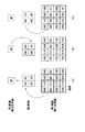
That is, for example, it is assumed that an added value of 4 pixels of 2 × 2 pixels (horizontal × vertical) is an upper layer pixel (pixel value), and three layer hierarchical encoding is performed. In this case, as an image in the lowest layer, for example, as shown in FIG. 9A, when 8 × 8 pixels are considered, the upper left 2 × 2 pixels of 4 pixels h00, h10, h01, h11 The added value m0 is calculated, and this is set as one pixel at the upper left of the second hierarchy. Similarly, the addition value m1 of the upper right four pixels h20, h31, h21, and h31, the addition value m2 of the lower left four pixels h02, h12, h03, and h13, and the lower right four pixels h22 and h32 of the image in the lowest hierarchy. , H23, and h33 are calculated, and each is set as one pixel in the upper right, lower left, and lower right of the second layer. Then, an added value q0 of 4 pixels m0, m1, m2, and m3 of 2 × 2 pixels in the second hierarchy is calculated, and this is set as a pixel of the image in the third hierarchy, that is, the highest hierarchy here.
[0006]
If all the pixels h00 to h33, m0 to m3, and q0 are stored as they are, the storage capacity is extra as much as the pixels m0 to m3 of the second hierarchy and q0 of the third hierarchy as described above. Etc. are required.
[0007]
Therefore, as shown in FIG. 9B, the pixel q0 in the third hierarchy is arranged, for example, at the position of the lower right pixel m3 among the pixels m0 to m3 in the second hierarchy. As a result, the second hierarchy is composed of the pixels m0 to m2 and q0.
[0008]
Then, as shown in FIG. 9C, the pixel m0 in the second hierarchy is, for example, the lower right pixel out of the pixels h00, h10, h01, h11 in the first hierarchy used for obtaining it. It arrange | positions in the position of the pixel h11. Similarly, the remaining pixels m1, m2, and q0 in the second hierarchy are arranged in place of the pixels h31, h13, and h33 in the first hierarchy. The pixel q0 is not directly obtained from the pixels h22, h32, h23, and h33, but is arranged in the second layer instead of m3 obtained directly from the pixels h22, h32, h23, and h33. Instead of arranging the pixel m3 at the position, the pixel q0 is arranged.
[0009]
As described above, as shown in FIG. 9C, the total number of pixels becomes 16 pixels of 4 × 4, which is not different from the case of only the pixels in the lowest hierarchy shown in FIG. Therefore, in this case, an increase in storage capacity or the like can be reduced.
[0010]
Decoding of the pixels m3 and h33 replaced with the pixel q0 and the pixels h11, h31, and h13 replaced with the pixels m0 to m2 can be performed as follows.
[0011]
That is, since q0 is an added value of m0 to m3, the expression q0 = m0 + m1 + m2 + m3 holds. Therefore, m3 can be obtained by the equation m3 = q0− (m0 + m1 + m2).
[0012]
Since m0 is an added value of h00, h10, h01, and h11, the expression m0 = h00 + h10 + h01 + h11 holds. Therefore, h11 can be obtained by the equation h11 = m0− (h00 + h10 + h01). Similarly, h31, h13, and h33 can be obtained. Note that h33 is obtained after obtaining m3 as described above.
[0013]
[Problems to be solved by the invention]
By the way, the hierarchical encoding as described above is conventionally performed in addition to a general-purpose memory (for example, SRAM (Static Random Access Memory) or DRAM (Dynamic RAM)) that stores the hierarchical encoding result. A delay circuit or the like for performing a line delay of pixels (pixel values) in one layer is necessary.
[0014]
That is, for example, in the case shown in FIG. 9C, in order to obtain the pixel h11 of the first layer that is not stored, it is necessary to calculate the expression h11 = m0− (h00 + h10 + h01). The pixels h00 and h10 on the first line and the pixels h01 and m0 on the second line are required. Assuming that reading of image data from the memory is sequentially performed in units of lines from the top to the bottom, the line starting with h00 is delayed by one line and waiting for the line starting with h01 to be read. That is, it is necessary to calculate the pixel h11 after waiting for the pixels m0, h00, h10, h01, which are necessary for calculating the pixel h11, to be read.
[0015]
As described above, conventionally, in addition to the memory, a delay circuit for performing line delay of the image data is necessary, and there is a problem that the apparatus becomes large.
[0016]
The present invention has been made in view of such circumstances, and is intended to reduce the size of the apparatus.
[0017]
[Means for Solving the Problems]
The storage device according to
[0018]
Claim4In the access method described in the above, an addition value of data written to each of the plurality of addresses of the first storage unit corresponding to each address included in the block of the second storage unit specified by the address specification information is obtained, Calculate hierarchical dataIn the middle of processingThe first processing data, which is data, is written to each address of the second storage means, and the read / write means in the second processing is stored in the block of the first storage means specified by the address designation information. The input image data stored at the included address is read, the first processing data of the second storage means specified based on the address designation information is read, and the input image data is read from the first processing data. By subtracting, the input image data not stored in the first storage means is calculated.In the middle of processingCalculating second processing data as data, and simultaneously executing the second processing for writing the second processing data to the address of the second storage means in which the first processing data was stored. Features.
[0019]
The storage device according to
[0020]
Claim4In the access method described inDuring the process of calculating hierarchical data by obtaining an added value of data written to each of a plurality of addresses of the first storage unit corresponding to each address included in the block of the second storage unit specified by the address specification information The first processing data that is the first data is stored in the address included in the block of the first storage means designated by the address designation information, and the first processing for writing the first processing data to each address of the second storage means By reading the input image data, reading the first processing data of the second storage means specified based on the addressing information, and subtracting the input image data from the first processing data, the first Second processing data that is data in the process of calculating input image data that is not stored in the storage means is calculated, and the second processing data is calculated. A second processing is performed at the same time written to the address of the second storage means the first processing data is stored.
[0026]
DETAILED DESCRIPTION OF THE INVENTION
FIG. 1 shows a configuration example of an embodiment of a storage device to which the present invention is applied.
[0027]
This storage device is composed of, for example, a one-chip CMOS (Complementary Metal Oxide Semiconductor) or the like, and performs hierarchical encoding that forms, for example, a three-layer image having a different number of pixels from an input image input thereto. Has been made.
[0028]
That is, the
[0029]
In the present embodiment, for example, as shown in FIG. 2, an image (digital image data) in which one screen is composed of 512 pixels in the horizontal direction and 512 lines in the vertical direction is input. Therefore, the horizontal address and the vertical address are both 9 (= log2512) represented in bits.
[0030]
The
[0031]
Here, the R / W signal is a signal for instructing reading of image data from the storage device or writing of image data to the storage device, and the hierarchy flag is used when reading an image stored in the storage device. For example, it is a 2-bit flag for instructing which one of the first to third layer images to be described later is read. Note that the image data is written to the
[0032]
The first
[0033]
The second
[0034]
The third
[0035]
Note that a clock is supplied to the
[0036]
The
[0037]
Next, the operation will be described with reference to FIGS.
[0038]
Here, as shown in FIG. 2 described above, one screen is composed of 512 × 512 pixels, and image data in which each pixel is represented by 8 bits is supplied to the storage device as an image of the first layer. Shall be. The image data is supplied by being sequentially scanned.
[0039]
Further, the pixel constituting the first layer image is h (0, 0) in the upper left pixel, and the pixel in the x + 1th position from the left and the y + 1th position from the top is set to h (x , Y). Since the first layer image is composed of 512 × 512 pixels as described above, both x and y are 0 to 511 (= 2).9It takes an integer value in the range of −1).
[0040]
Also, 0 to 255 (= 29Considering the variables s and t taking integer values in the range of / 2-1), the pixels constituting the second layer image are 2 × 2 pixels adjacent to the first layer.
h (2s, 2t), h (2s + 1, 2t),
h (2s, 2t + 1), h (2s + 1, 2t + 1)
Is represented by m (s, t). Therefore, the formula
m (s, t) = h (2s, 2t) + h (2s + 1,2t) + h (2s, 2t + 1) + h (2s + 1,2t + 1) (1)
Holds.
[0041]
Furthermore, 0 to 127 (= 29Considering the variables m and n taking integer values in the range of / 4-1), the pixels constituting the third layer image are adjacent 2 × 2 pixels of the second layer.
m (2m, 2n), m (2m + 1, 2n),
m (2m, 2n + 1), m (2m + 1, 2n + 1)
Value, that is, adjacent 4 × 4 pixels in the first layer
h (4m, 4n), h (4m + 1,4n), h (4m + 2,4n), h (4m + 3,4n),
h (4m, 4n + 1), h (4m + 1,4n + 1), h (4m + 2,4n + 1), h (4m + 3,4n + 1),
h (4m, 4n + 2), h (4m + 1,4n + 2), h (4m + 2,4n + 2), h (4m + 3,4n + 2),
h (4m, 4n + 3), h (4m + 1,4n + 3), h (4m + 2,4n + 3), h (4m + 3,4n + 3)
It is expressed as q (m, n). Therefore, the formula
q (m, n) = m (2m, 2n) + m (2m + 1,2n) + m (2m, 2n + 1) + m (2m + 1,2n + 1)
= h (4m, 4n) + h (4m + 1,4n) + h (4m + 2,4n) + h (4m + 3,4n)
+ h (4m, 4n + 1) + h (4m + 1,4n + 1) + h (4m + 2,4n + 1) + h (4m + 3,4n + 1)
+ h (4m, 4n + 2) + h (4m + 1,4n + 2) + h (4m + 2,4n + 2) + h (4m + 3,4n + 2)
+ h (4m, 4n + 3) + h (4m + 1,4n + 3) + h (4m + 2,4n + 3) + h (4m + 3,4n + 3) (2)
Holds.
[0042]
The
(0,0), (1,0), ..., (511,0),
(0, 1), (1, 1), ..., (511, 1),
・
・
・
(511,0), (511,1), ..., (511,511)
In this order (the order corresponding to the sequential scanning), the signals are supplied in synchronization with the clock.
[0043]
Further, each bit of the 9-bit horizontal address HA is represented as ha1, ha2,..., Ha8 (ha8 is the most significant bit) with its least significant bit ha0, and each bit of the 9-bit vertical address VA. Similarly, va0 is represented as va1, va2,..., Va8 (va8 is the most significant bit) with the least significant bit as va0.
[0044]
At the time of writing image data to the storage device, the first layer image is sequentially scanned and supplied to the
[0045]
In this case, access to the
[0046]
That is, as shown in FIG. 3, at the time of writing (when the R / W signal indicates writing), the
(0,0), (1,0), ..., (511,0),
(0, 1), (1, 1), ..., (511, 1),
...
(511,0), (511,1), ..., (511,511)
Includes the first layer pixel (pixel value)
h (0,0), h (1,0),..., h (511,0),
h (0, 1), h (1, 1), ..., h (511, 1),
...
h (511,0), h (511,1),..., h (511,511)
Are stored respectively.
[0047]
At the time of reading (when the R / W signal indicates reading), the
[0048]
Next, access to the
[0049]
First, at the time of writing, as shown in FIG. 4, for example, the
[0050]
Therefore, for example, 2 × 2 4 pixels h (2s, 2t), h (2s + 1, 2t), h (2s, 2t + 1), h (2s + 1, 2t + 1) in the first layer as indicated by D1 in FIG. At any timing supplied to the
[0051]
On the other hand, in the
[0052]
The
[0053]
The
[0054]
The
[0055]
Accordingly, the upper left pixel h (2s, 2t) among the 2 × 2 pixels h (2s, 2t), h (2s + 1, 2t), h (2s, 2t + 1), h (2s + 1, 2t + 1) in the first layer is obtained. At the timing supplied to the
[0056]
As a result, 0 is supplied to the
[0057]
In the
[0058]
Next, the upper left pixel h (2s, 2t) of the 2 × 2 pixels h (2s, 2t), h (2s + 1, 2t), h (2s, 2t + 1), h (2s + 1, 2t + 1) in the first layer At the timing at which the pixel h (2s + 1, 2t) on the right side of the signal is supplied to the
[0059]
On the other hand, in this case, since the least significant bit ha0 of the horizontal address HA is 1 and the least significant bit va0 of the vertical address VA is 0, the output of the NOR
[0060]
As a result, the data (stored data) read in the reading unit 11 (here, 0 + h (2s, 2t)) is supplied to the
[0061]
In the
[0062]
Thereafter, the supply of image data on the 2t + 1 line from the top of the first layer is started, and 2 × 2 pixels h (2s, 2t), h (2s + 1, 2t), h (2s, 2t + 1), h of the first layer are started. When the lower left pixel h (2s, 2t + 1) of (2s + 1, 2t + 1) is supplied to the
[0063]
On the other hand, in this case, since the least significant bit ha0 of the horizontal address HA is 0 and the least significant bit va0 of the vertical address VA is 1, the output of the NOR
[0064]
As a result, the data (stored data) read in the reading unit 11 (here, 0 + h (2s, 2t) + h (2s + 1, 2t)) is supplied to the
[0065]
The
[0066]
Next, the lower left pixel h (2s, 2t + 1) of 2 × 2 pixels h (2s, 2t), h (2s + 1, 2t), h (2s, 2t + 1), h (2s + 1, 2t + 1) in the first layer When the pixel h (2s + 1, 2t + 1) on the right side is supplied to the
[0067]
On the other hand, in this case, since the least significant bit ha0 of the horizontal address HA and the least significant bit va0 of the vertical address VA are both 1, the output of the NOR
[0068]
As a result, the
[0069]
The
[0070]
Therefore, the address (s, t) of the second
[0071]
As described above, the
[0072]
As described above, the first layer image data is written to the address (HA, VA) of the
[0073]
Further, in this case, the
[0074]
Next, reading of the second layer image from the
[0075]
At the time of reading, when the hierarchy flag indicates the second hierarchy, the
[0076]
On the other hand, in the
[0077]
That is, from the above, when the set of the horizontal address HA and the vertical address VA is (2s, 2t), (2s + 1, 2t), (2s, 2t + 1), (2s + 1, 2t + 1), the
[0078]
Therefore, in the
[0079]
The second layer image data read by the
[0080]
As described above, the second hierarchy image stored in the
[0081]
Next, access to the
[0082]
First, at the time of writing, as shown in FIG. 5, for example, the
[0083]
Therefore, for example, as shown by D2 in FIG. 2, 4 × 4 16 pixels h (4m, 4n), h (4m + 1, 4n), h (4m + 2, 4n), h (4m + 3, 4n), h (4m, 4n + 1), h (4m + 1, 4n + 1), h (4m + 2, 4n + 1), h (4m + 3, 4n + 1), h (4m, 4n + 2), h (4m + 1, 4n + 2), h (4m + 2, 4n + 2), h (4m + 3, 4n + 2), h (4m, 4n + 3), h (4m + 1, 4n + 3), h (4m + 2, 4n + 3), h (4m + 3, 4n + 3) are supplied to the
[0084]
On the other hand, in the
[0085]
The
[0086]
The
[0087]
The
[0088]
Therefore, at the timing when the pixel h (4m, 4n) in the first hierarchy is supplied to the
[0089]
As a result, 0 is supplied to the
[0090]
In the
[0091]
Next, at the timing when the pixel h (4m + 1, 4n) on the right side of the pixel h (4m, 4n) in the first hierarchy is supplied to the
[0092]
On the other hand, in this case, the lower 2 bits ha0 or ha1 of the horizontal address HA are 1 or 0, respectively, and the lower 2 bits va0 and va1 of the vertical address VA are both 0. Therefore, the output of the NOR
[0093]
As a result, the data (stored data) read in the reading unit 21 (here, 0 + h (4m, 4n)) is supplied to the
[0094]
In the
[0095]
Next, at the timing when the pixel h (4m + 2, 4n) on the right side of the pixel h (4m + 1, 4n) in the first hierarchy is supplied to the
[0096]
On the other hand, in this case, since the lower 2 bits ha0 or ha1 of the horizontal address HA are 0 or 1, respectively, and the lower 2 bits va0 and va1 of the vertical address VA are both 0, the output of the NOR
[0097]
As a result, the data (stored data) read in the reading unit 21 (here, 0 + h (4m, 4n) + h (4m + 1, 4n)) is supplied to the
[0098]
In the
[0099]
Hereinafter, pixels h (4m + 3, 4n), h (4m, 4n + 1), h (4m + 1, 4n + 1), h (4m + 2, 4n + 1), h (4m + 3, 4n + 1), h (4m, 4n + 2), h in the first layer (4m + 1, 4n + 2), h (4m + 2, 4n + 2), h (4m + 3, 4n + 2), h (4m, 4n + 3), h (4m + 1, 4n + 3), h (4m + 2, 4n + 3), h (4m + 3, 4n + 3) In any case, the same processing as described above is performed at the timing supplied to the
[0100]
As described above, the
[0101]
Accordingly, at the same time as storing the image data of the first layer, the image data of the second layer, and further, the image data of the third layer can be generated and stored. That is, the second and third layer image data can be obtained in real time.
[0102]
In this case as well, the
[0103]
Next, reading of the third layer image from the
[0104]
At the time of reading, when the hierarchy flag indicates the third hierarchy, the
[0105]
On the other hand, in the
[0106]
That is, from the above, the set of the horizontal address HA and the vertical address VA is (4m, 4n), (4m + 1, 4n), (4m + 2, 4n), (4m + 3, 4n), (4m, 4n + 1), ( 4m + 1, 4n + 1), (4m + 2, 4n + 1), (4m + 3, 4n + 1), (4m, 4n + 2), (4m + 1, 4n + 2), (4m + 2, 4n + 2), (4m + 3, 4n + 2), (4m, 4n + 3), (4m + 1, In the case of (4n + 3), (4m + 2, 4n + 3), (4m + 3, 4n + 3), the
[0107]
Therefore, in the
[0108]
The third layer image data read by the
[0109]
As described above, from the
[0110]
The reading of the image data of the second hierarchy from the
[0111]
Next, from what has been described with reference to FIG. 9, among the adjacent 2 × 2 pixels h (2s, 2t), h (2s + 1, 2t), h (2s, 2t + 1), and h (2s + 1, 2t + 1) in the first layer For example, the lower right pixel h (2s + 1, 2t + 1) is the remaining first layer pixel h (2s, 2t), h (2s + 1, 2t), h (2s, 2t + 1), and Can be obtained from the pixel m (s, t) in the second layer, which is the added value of.
[0112]
That is, the pixel h (2s + 1, 2t + 1) in the first layer
h (2s + 1,2t + 1) = m (s, t)-(h (2s, 2t) + h (2s + 1,2t) + h (2s, 2t + 1))
Can be obtained.
[0113]
Therefore, the pixel h (2s + 1, 2t + 1) in the first layer can be obtained from the above equation without being stored.
[0114]
Therefore, the
[0115]
That is, in the above case, the
[0116]
Further, it is one of adjacent 2 × 2 pixels m (2m, 2n), m (2m + 1, 2n), m (2m, 2n + 1), m (2m + 1, 2n + 1) in the second layer, for example, right The lower pixel m (2m + 1, 2n + 1) is also the remaining second-layer pixel m (2m, 2n), m (2m + 1, 2n), m (2m, 2n + 1), and the third added value thereof. It can be obtained from the pixel q (m, n) of the hierarchy.
[0117]
That is, the pixel m (2m + 1, 2n + 1) in the second hierarchy is expressed by the equation
m (2m + 1,2n + 1) = q (m, n)-(m (2m, 2n) + m (2m + 1,2n) + m (2m, 2n + 1))
Can be obtained.
[0118]
Accordingly, the pixel m (2m + 1, 2n + 1) in the second layer can be obtained without being stored.
[0119]
Therefore, the
[0120]
That is, in the above-described case, the second
[0121]
Even when the
[0122]
Similarly, the
[0123]
Further, the third layer image stored in the storage device can be read in the same manner as in FIG. 5 described above. However, the first or second layer image can be read as follows. Is called.
[0124]
That is, FIG. 6 shows a configuration example of the storage device of FIG. 1 when reading the image of the first hierarchy when the storage capacity of the
[0125]
In this case, the
[0126]
That is, the
[0127]
Here, the horizontal address HA or vertical address VA four lines before generated by the
[0128]
The delayed horizontal address HA and the delayed vertical address VA are supplied to the
[0129]
In addition to the delayed horizontal address HA and the delayed vertical address VA, the
[0130]
That is, for example, when the
[0131]
The
[0132]
What is selected as the A bank address or the B bank address in the
[0133]
The
[0134]
What is selected as the A bank address or the B bank address in the
[0135]
In the embodiment of FIG. 6 (the same applies to FIG. 8 described later), the address space of the first
[0136]
An address terminal (A bank address terminal) for accessing the A bank and an address terminal (B bank address terminal) for accessing the B bank so that both the A bank and the B bank can be accessed simultaneously. These two address terminals are provided. Furthermore, two data terminals, that is, an A bank data terminal and a B bank data terminal, are provided as input / output terminals for reading / writing data from / to the A bank and B bank.
[0137]
Therefore, in the first
[0138]
In this embodiment, the delayed horizontal address HA and the delayed vertical address VA are obtained by delaying the horizontal address HA and the vertical address VA by 4 lines (4 lines of the first stage image). Therefore, in the
[0139]
That is, for example, as shown in FIG. 7, if the first-
[0140]
Returning to FIG. 6, in the
[0141]
In the
[0142]
Both the A bank data terminal and the B bank data terminal from which data (A bank data or B bank data) read from the A bank or B bank of the
[0143]
That is, at a certain point in time, for example, when the A bank data terminal or the B bank data terminal is connected to the
[0144]
The data to be written to the A bank of the second
[0145]
That is, the
[0146]
The data to be written to the A bank of the
[0147]
The
[0148]
The
[0149]
The
[0150]
The switch 61 selects one of the terminals 61a and 61b corresponding to the output of the AND
[0151]
Here, the above selection circuits 41 to 43, reading
[0152]
In FIG. 6 (the same applies to FIG. 8 described later), the clock, the R / W signal, and the hierarchy flag are not shown.
[0153]
Next, the operation will be described.
[0154]
Now, in the
[0155]
In this case, in the
[0156]
The A bank address and the B bank address selected by the
[0157]
Further, in this case, in the selection circuit 41, the A bank data terminal of the first
[0158]
The
[0159]
When the output of the AND
[0160]
On the other hand, the readout unit 47 reads out the pixel (pixel value) in the second hierarchy stored in the A bank address output from the
[0161]
Here, at the timing when access is made to 2 × 2 4 pixels h (2s, 2t), h (2s + 1, 2t), h (2s, 2t + 1), h (2s + 1, 2t + 1) in the first hierarchy, In the case where access is made to the A bank addresses (2s, 2t), (2s + 1, 2t), (2s, 2t + 1), (2s + 1, 2t + 1) of the
[0162]
Therefore, when the
[0163]
In the
[0164]
Therefore, at first, the A bank address (s, t) of the
[0165]
Further, the
[0166]
Thereafter, the
[0167]
Accordingly, the A bank address (2s + 1, 2t + 1) of the first layer memory 2 (here, there is no memory cell corresponding to this address, and therefore, nothing is written, for example, even if this address is accessed) The data read from the A bank address (s, t) of the second
[0168]
On the other hand, when only the output of the AND
[0169]
On the other hand, the
[0170]
Here, 4 × 4 16 pixels h (4m, 4n), h (4m + 1, 4n), h (4m + 2, 4n), h (4m + 3, 4n), h in the first layer as shown by D2 in FIG. (4m, 4n + 1), h (4m + 1, 4n + 1), h (4m + 2, 4n + 1), h (4m + 3, 4n + 1), h (4m, 4n + 2), h (4m + 1, 4n + 2), h (4m + 2, 4n + 2), h ( 4m + 3, 4n + 2), h (4m, 4n + 3), h (4m + 1, 4n + 3), h (4m + 2, 4n + 3), and h (4m + 3, 4n + 3) are accessed at any timing from the above. The A bank address (m, n) of the
[0171]
Accordingly, the
[0172]
The switch 61 selects the terminal 61a when the output of the AND
[0173]
In addition, as described above, the reading unit 47 performs pixels h (4m + 1, 4n + 1), h (4m + 3, 4n + 1), corresponding to the lower right pixel h (2s + 1, 2t + 1) of the 2 × 2 pixels in the first layer, When outputting h (4m + 1, 4n + 3), that is, when the output of the AND
[0174]
In the
[0175]
Therefore, at first, the A-bank address (m, n) of the third-
[0176]
Further, the
[0177]
Thereafter, similarly, the stored value of the A bank address (m, n) of the
[0178]
When the reading unit 47 reads out the first layer pixel h (4m + 1, 4n + 1) corresponding to the lower right pixel h (2s + 1, 2t + 1) of the 2 × 2 pixels in the first layer, As described above, the data is supplied to the
[0179]
In the
[0180]
Thereafter, in the same manner, finally, that is, the
[0181]
Therefore, the A bank address (4m + 3, 4n + 3) of the first layer memory 2 (here, there is no memory cell corresponding to this address, and therefore, nothing is written, for example, nothing is accessed even if this address is accessed. The data read by the
[0182]
On the other hand, when both the outputs of the AND
[0183]
By the way, when pixels in the first layer are read out as described above, the pixels h (2s + 1, 2t + 1) (however, h (4m + 3, 4n + 3) in the first layer are stored in the
[0184]
That is, the stored value of the
[0185]
Therefore, it is necessary to return the stored values of the
[0186]
Therefore, as described above, the
[0187]
In this embodiment, the delayed horizontal address HA and the delayed vertical address VA are obtained by delaying the horizontal address HA and the vertical address VA by four lines, and as described above, the horizontal address HA and the vertical address VA. Is selected as the A bank address, and the delayed horizontal address HA and the delayed vertical address VA are selected as the B bank addresses, respectively, in the
[0188]
Similarly, in the second
[0189]
Therefore, when the
[0190]
When the
[0191]
In the
[0192]
Therefore, at first, the B bank address (s, t ′) of the
[0193]
Further, the
[0194]
After that, the
[0195]
In addition, the
[0196]
Further, in this case, in the
[0197]
The
[0198]
In the
[0199]
Therefore, at first, the A bank address (m, n ′) of the
[0200]
Further, the
[0201]
Thereafter, similarly, finally, that is, the
[0202]
Thereafter, when the lower third bit va2 of the vertical address VA changes, in the
[0203]
In this case, in the
[0204]
The A bank address and the B bank address selected by the
[0205]
Further, in the selection circuit 41, the B bank data terminal of the
[0206]
Then, a process is performed in which A bank or B bank in the above-described process is replaced with B bank or A bank, respectively.
[0207]
Thereafter, the same processing is performed, and the first layer pixels are output from the
[0208]
Next, FIG. 8 shows the storage device shown in FIG. 1 when reading the image of the second hierarchy when the
[0209]
In this case, the
[0210]
Also, the
[0211]
Further, the
[0212]
Both the A bank data terminal and the B bank data terminal from which data (A bank data or B bank data) read from the A bank or B bank of the second
[0213]
That is, at a certain point in time, for example, when the A bank data terminal or the B bank data terminal is connected to the
[0214]
The data to be written to the A bank of the
[0215]
That is, the selection circuit 82 is controlled at a certain point in time when, for example, the A bank data terminal is connected to the writing unit 86 and the reading unit 87 and the B bank data terminal is connected to the writing unit 88 and the reading unit 89. When the signal va2 changes, the A bank data terminal is connected to the writing unit 88 and the reading unit 89, and the B bank terminal is connected to the writing unit 86 and the reading unit 87. Further, after that, when the control signal va2 changes again, the selection circuit 82 reconnects the A bank data terminal to the writing unit 86 and the reading unit 87, and reconnects the B bank data terminal to the writing unit 88 and the reading unit 89. To do. Therefore, according to the selection circuit 82, every time the control signal va2 changes, the A bank data terminal is alternately connected to the writing unit 86 and the reading unit 87, or the writing unit 88 and the reading unit 89, and the B bank. Data terminals are alternately connected to the writing unit 88 and the reading unit 89 or between the writing unit 86 and the reading unit 87.
[0216]
The
[0217]
The switch 91 selects one of the terminals 91a and 91b corresponding to the output of the AND gate 99, and the output is supplied to the arithmetic unit 94. Note that 0 is supplied to the terminal 91b. The switch 92 selects one of the
[0218]
The arithmetic unit 94 subtracts the output of the switch 91 from the output of the reading unit 87 and supplies the subtraction result to the writing unit 86. The
[0219]
The selection circuit 98 selects and outputs one of the outputs of the reading unit 84 or 87 corresponding to the outputs of the AND
[0220]
Next, the operation will be described.
[0221]
Now, in the
[0222]
That is, in the
[0223]
The A bank address and the B bank address selected by the
[0224]
Further, in this case, in the
[0225]
The readout unit 84 reads out the second layer pixel (pixel value) stored in the A bank address output from the
[0226]
For example, when only the output of the AND gate 99 is 1 among the outputs of the AND
[0227]
On the other hand, from the above, the timing at which access is made to 2 × 2 4 pixels h (2s, 2t), h (2s + 1, 2t), h (2s, 2t + 1), h (2s + 1, 2t + 1) in the first layer. In any case, the pixel m (s, t) in the second layer is accessed. Therefore, at any timing when the 2 × 2 4 pixels h (2s, 2t), h (2s + 1, 2t), h (2s, 2t + 1), h (2s + 1, 2t + 1) in the first layer are accessed. If the data read from the
[0228]
Therefore, in the selection circuit 98, the lower right of the 2 × 2 4 pixels h (2s, 2t), h (2s + 1, 2t), h (2s, 2t + 1), h (2s + 1, 2t + 1) in the first layer The output of the reading unit 84, that is, the pixel m (s, t) in the second layer is selected only at the timing when the pixel h (2s + 1, 2t + 1) (except the pixel h (4m + 3, 4n + 3)) is read out. Is output.
[0229]
For the same reason, the switch 91 also selects the terminal 91b only at the timing when the pixel h (2s + 1, 2t + 1) in the first layer is output from the readout unit 84 (the timing when the output of the AND gate 99 becomes 1). In other cases, the terminal 91a is selected. In other words, the arithmetic unit 94 has 2 × 2 4 pixels h (2s, 2t), h (2s + 1, 2t), h (2s, 2t + 1), h (2s + 1, 2t + 1) in the first layer. Only at the timing when the lower right pixel h (2s + 1, 2t + 1) is read out, the pixel m (s, t) of the second hierarchy output from the reading unit 84 is supplied, and 0 is supplied in other cases.
[0230]
On the other hand, the readout unit 87 reads out the third layer pixel (pixel value) stored in the A bank address output from the
[0231]
That is, in the reading unit 87, the addresses (4m, 4n), (4m + 1, 4n), (4m + 2, 4n), (4m + 3, 4n), (4m, 4n + 1), (4m + 1, 4n + 1), (4m + 1, 4n + 1), (4m + 2, 4n + 1), (4m + 3, 4n + 1), (4m, 4n + 2), (4m + 1, 4n + 2), (4m + 2, 4n + 2), (4m + 3, 4n + 2), (4m, 4n + 3), (4m + 1, 4n + 3), (4m + 2) , 4n + 3), (4m + 3, 4n + 3), the data is read from the A bank address (m, n) of the
[0232]
As described above, the switch 91 is an address excluding (4m + 1, 4n + 1), (4m + 3, 4n + 1), (4m + 1, 4n + 3), and (4m + 3, 4n + 3) corresponding to the address (2s + 1, 2t + 1) of the
[0233]
On the other hand, at the timing when the addresses (4m + 1, 4n + 1), (4m + 3, 4n + 1), and (4m + 1, 4n + 3) of the
[0234]
In the arithmetic unit 94, the output of the reading unit 84 is subtracted from the output of the reading unit 87 and supplied to the writing unit 86. The writing unit 86 writes the output of the arithmetic unit 94 to the A bank address (m, n) of the
[0235]
Therefore, at first, the A bank address (m, n) of the
[0236]
The arithmetic unit 94 obtains these subtraction values (q (m, n) -m (2m, 2n)) and writes them in the A bank address (m, n) of the
[0237]
Further, at the timing when the address (4m + 3, 4n + 1) of the
[0238]
The arithmetic unit 94 obtains these subtraction values (q (m, n) −m (2m, 2n) −m (2m + 1,2n)), and the writing unit 86 uses the A bank address ( m, n).
[0239]
Thereafter, when it is time to access the address (4m + 1, 4n + 3) of the
[0240]
The arithmetic unit 94 obtains these subtraction values (q (m, n) -m (2m, 2n) -m (2m + 1,2n) -m (2m, 2n + 1)). The data is written to the A bank address (m, n) of the
[0241]
That is, the A bank address (m, n) of the
[0242]
Therefore, the A bank address (4m + 3, 4n + 3) of the first layer memory 2 (here, there is no memory cell corresponding to this address, and therefore, nothing is written, for example, nothing is accessed even if this address is accessed. At the timing when access is made at the time of not being read (the timing at which access is made to the A bank address (2m + 1, 2n + 1) of the second hierarchy memory 3 (there is no memory cell corresponding to this address)) The data read out from the A bank address (m, n) of the
[0243]
On the other hand, when both the outputs of the AND
[0244]
By the way, when the pixels of the second hierarchy are read out as described above, the pixels m (2m + 1, 2n + 1) of the second hierarchy are stored in the
[0245]
That is, the stored value of the
[0246]
Therefore, it is necessary to return the stored value of the
[0247]
Therefore, as described above, for example, when the horizontal address HA and the vertical address VA are selected as the A bank address and the delayed horizontal address HA and the delayed vertical address VA are selected as the B bank address, respectively, the first
[0248]
Similarly, in the second
[0249]
Therefore, when the reading unit 84 reads the pixels m (2m, 2n), m (2m + 1, 2n), and m (2m, 2n + 1) in the second layer from the A bank of the
[0250]
Similarly to the switch 91, the switch 92 selects the terminal 92b only at the timing when the pixel h (2s + 1, 2t + 1) in the first layer is output from the reading unit 84 (the timing when the output of the AND gate 99 becomes 1). In other cases, the
[0251]
When the
[0252]
In the
[0253]
Therefore, at first, the B bank address (m, n ′) of the
[0254]
Further, the
[0255]
Thereafter, the
[0256]
Thereafter, when the lower third bit va2 of the vertical address VA changes, the selection of the A bank address and the B bank address is changed in the
[0257]
The A bank address and the B bank address selected by the
[0258]
Further, in the
[0259]
Then, a process is performed in which A bank or B bank in the above-described process is replaced with B bank or A bank, respectively.
[0260]
Thereafter, the same processing is performed, and the pixels of the second hierarchy are output from the selection circuit 98, and the storage contents of the
[0261]
As described above, the
[0262]
That is, for example, the pixel of the first layer stored in the A bank address of the
[0263]
In the present embodiment, the
[0264]
In this embodiment, addition or subtraction is performed using data read from the A bank or B bank. However, processing using data read from the A bank or B bank is performed using addition or subtraction. It is not limited to subtraction.
[0265]
Further, in the present embodiment, the second
[0266]
In the present embodiment, the horizontal address or the vertical address corresponding to the horizontal or vertical position of the pixels constituting the image with respect to the first
[0267]
Furthermore, the
[0268]
In this embodiment, the
[0269]
Furthermore, in the present embodiment, the bit allocation amount of the pixels in the first hierarchy is 8 bits, and the data length of the memory cells in the
[0270]
That is, for example, as described above, when the storage capacities of the
[0271]
The present invention is applicable to both non-interlaced scanned images and interlaced scanned images.
[0272]
Furthermore, in the present embodiment, the number of hierarchies is three, but the number of hierarchies may be two, or four or more.
[0273]
In the present embodiment, the addition value of 2 × 2 4 pixels in the lower layer is set as the upper layer pixel (pixel value) that is one level higher. Is not limited to this.
[0274]
Furthermore, in the present embodiment, the present invention is realized by hardware, but the present invention can also be realized by causing a computer to execute a program that performs the above-described processing.
[0275]
In this embodiment, pixels (pixel values) are stored in a memory represented by, for example, a RAM (Random Access Memory). However, the pixels may be stored in, for example, a magnetic disk or a magneto-optical device. It is also possible to store (record) in a recording medium such as a disk, a magnetic tape, or an optical card.
[0276]
【The invention's effect】
According to the storage device according to
[Brief description of the drawings]
FIG. 1 is a block diagram showing a configuration example of an embodiment of a storage device of the present invention.
FIG. 2 is a diagram illustrating a configuration example of one screen of an image in a first layer.
FIG. 3 is a block diagram illustrating a first functional configuration example of the storage device of FIG. 1;
4 is a block diagram illustrating a second functional configuration example of the storage device of FIG. 1; FIG.
FIG. 5 is a block diagram illustrating a third functional configuration example of the storage device of FIG. 1;
6 is a block diagram illustrating a fourth functional configuration example of the storage device in FIG. 1; FIG.
7 is a diagram for explaining the first
FIG. 8 is a block diagram showing a fifth functional configuration example of the storage device of FIG. 1;
FIG. 9 is a diagram for explaining hierarchical encoding.
[Explanation of symbols]
DESCRIPTION OF
Claims (4)
その記憶領域へアクセスするためのアドレス空間が、前記記憶領域において異なる複数の範囲をさすように複数のブロックに分割され、各ブロックごとに、その記憶領域に記憶される前記入力画像データを構成する画素のうちの、後記第2の記憶手段に記憶される画素を除く画素のそれぞれについてアドレス指定が可能な第1の記憶手段と、
その記憶領域へアクセスするためのアドレス空間が、前記第1の記憶手段の記憶領域へアクセスするためのアドレス空間を構成するブロックと同一の数のブロックに分割され、各ブロックごとに、その記憶領域に記憶される前記階層データを構成する画素単位でアドレス指定が可能な第2の記憶手段と、
各ブロックに対応するアドレス指定情報に基づいて、前記第1の記憶手段の各ブロックそれぞれに対するアドレス指定を同時に行うとともに、前記アドレス指定情報を構成するビット列の一部によって前記第2の記憶手段の各ブロックそれぞれに対するアドレス指定を同時に行うアドレス指定手段と、
前記入力画像データを構成する画素のうち、前記所定の位置の複数の画素の画素値を順次加算することにより前記階層データを算出する第1の処理と、前記入力画像データを構成する画素のうち、前記所定の位置の複数の画素の画素値を前記階層データから順次減算することにより前記入力画像データを構成する画素の画素値を算出する第2の処理を同時に実行する読み書き手段と
を備え、
前記第1の処理において前記読み書き手段は、前記アドレス指定情報により指定された前記第2の記憶手段のブロックに含まれる各アドレスに対応する前記第1の記憶手段の複数のアドレスそれぞれに書き込まれるデータの加算値を求めて、前記階層データを算出する処理途中のデータである第1の処理データを、前記第2の記憶手段の前記各アドレスに書き込み、
前記第2の処理において前記読み書き手段は、前記アドレス指定情報により指定された前記第1の記憶手段のブロックに含まれるアドレスに記憶されている前記入力画像データを読み出すとともに、前記アドレス指定情報に基づいて特定される前記第2の記憶手段の、前記第1の処理データを読み出し、その入力画像データを前記第1の処理データから減算することにより、前記第1の記憶手段に記憶されていない前記入力画像データを算出する処理途中のデータである第2の処理データを算出し、その第2の処理データを、前記第1の処理データが記憶されていた前記第2の記憶手段のアドレスに書き込む
ことを特徴とする記憶装置。Image data composed of a smaller number of pixels than the input image data from the input image data, and obtained by adding pixel values of a plurality of pixels at predetermined positions among the pixels constituting the input image data. The input value is used when performing hierarchical encoding by calculating hierarchical data, which is image data composed of one pixel determined corresponding to the plurality of pixels. A storage device for storing data and the hierarchical data,
An address space for accessing the storage area is divided into a plurality of blocks so as to indicate a plurality of different ranges in the storage area, and the input image data stored in the storage area is configured for each block. First storage means capable of addressing each of the pixels excluding the pixels stored in the second storage means described later ,
The address space for accessing the storage area is divided into the same number of blocks as the blocks constituting the address space for accessing the storage area of the first storage means, and for each block , the storage area Second storage means capable of addressing in units of pixels constituting the hierarchical data stored in
Based on the address designation information corresponding to each block, address designation for each block of the first storage means is simultaneously performed, and each of the second storage means is determined by a part of the bit string constituting the address designation information. Addressing means for simultaneously addressing each block;
Of the pixels constituting the input image data, a first process for calculating the hierarchical data by sequentially adding pixel values of a plurality of pixels at the predetermined position, and among the pixels constituting the input image data Read / write means for simultaneously executing a second process of calculating pixel values of pixels constituting the input image data by sequentially subtracting pixel values of a plurality of pixels at the predetermined position from the hierarchical data ,
In the first process, the read / write means writes data to each of the plurality of addresses of the first storage means corresponding to each address included in the block of the second storage means designated by the address designation information. The first processing data, which is data in the middle of calculating the hierarchical data, is written to each address of the second storage means,
In the second process, the read / write unit reads the input image data stored in the address included in the block of the first storage unit designated by the address designation information, and based on the address designation information The first processing data of the second storage means specified in the above is read out, and the input image data is subtracted from the first processing data, thereby not being stored in the first storage means. Second processing data, which is data in the process of calculating the input image data, is calculated, and the second processing data is written to the address of the second storage means in which the first processing data was stored. A storage device.
ことを特徴とする請求項1に記載の記憶装置。The said address designation means produces | generates the information which specifies a different address for each block of the said 1st memory | storage means by performing a predetermined process to the input address designation information. Storage device.
ことを特徴とする請求項1に記載の記憶装置。The storage device according to claim 1 , wherein the address designation information corresponds to a position in a horizontal direction or a vertical direction of pixels constituting the input image data.
前記アドレス指定情報により指定された前記第2の記憶手段のブロックに含まれる各アドレスに対応する前記第1の記憶手段の複数のアドレスそれぞれに書き込まれるデータの加算値を求めて、前記階層データを算出する処理途中のデータである第1の処理データを、前記第2の記憶手段の前記各アドレスに書き込む第1の処理と、
前記第2の処理において前記読み書き手段は、前記アドレス指定情報により指定された前記第1の記憶手段のブロックに含まれるアドレスに記憶されている前記入力画像データを読み出すとともに、前記アドレス指定情報に基づいて特定される前記第2の記憶手段の、前記第1の処理データを読み出し、その入力画像データを前記第1の処理データから減算することにより、前記第1の記憶手段に記憶されていない前記入力画像データを算出する処理途中のデータである第2の処理データを算出し、その第2の処理データを、前記第1の処理データが記憶されていた前記第2の記憶手段のアドレスに書き込む第2の処理とを、
同時に実行する
ことを特徴とするアクセス方法。Image data composed of a smaller number of pixels than the input image data from the input image data, and obtained by adding pixel values of a plurality of pixels at predetermined positions among the pixels constituting the input image data. The input value is used when performing hierarchical encoding by calculating hierarchical data, which is image data composed of one pixel determined corresponding to the plurality of pixels. Oite a storage device for storing the data and the hierarchical data, the address space for accessing the storage area is divided into a plurality of blocks to point multiple ranges differ in the storage area, for each block Among the pixels constituting the input image data stored in the storage area, excluding the pixels stored in the second storage means described later. First storage means capable addressable Te, the address space for accessing the storage area, the first number the same as blocks constituting the address space for accessing the storage area of the storage means Based on the second storage means that is divided into blocks and can be addressed in units of pixels constituting the hierarchical data stored in the storage area for each block, and addressing information corresponding to each block, Address designation means for simultaneously performing address designation for each block of the first storage means and simultaneously performing address designation for each block of the second storage means by a part of a bit string constituting the address designation information; The pixel values of a plurality of pixels at the predetermined position among the pixels constituting the input image data are sequentially added. A first processing for calculating the hierarchical data by, among pixels constituting the input image data, the input image by sequentially subtracting the pixel values of a plurality of pixels of the predetermined position from the hierarchical data an access method against the storage device and a write means for executing a second process for calculating the pixel values of the pixels constituting the data at the same time,
An addition value of data written to each of a plurality of addresses of the first storage unit corresponding to each address included in the block of the second storage unit specified by the address specification information is obtained, and the hierarchical data is obtained. A first process for writing first process data, which is data in the process of calculation, to each address of the second storage unit;
In the second process, the read / write unit reads the input image data stored in the address included in the block of the first storage unit designated by the address designation information, and based on the address designation information The first processing data of the second storage means specified in the above is read out, and the input image data is subtracted from the first processing data, thereby not being stored in the first storage means. Second processing data, which is data in the process of calculating the input image data, is calculated, and the second processing data is written to the address of the second storage means in which the first processing data was stored. The second process,
An access method characterized by being executed simultaneously.
Priority Applications (7)
| Application Number | Priority Date | Filing Date | Title |
|---|---|---|---|
| JP20437397A JP4236713B2 (en) | 1997-07-30 | 1997-07-30 | Storage device and access method |
| US09/121,419 US6252611B1 (en) | 1997-07-30 | 1998-07-23 | Storage device having plural memory banks concurrently accessible, and access method therefor |
| SG9802662A SG81239A1 (en) | 1997-07-30 | 1998-07-24 | Storage device and access method |
| AU78588/98A AU748297B2 (en) | 1997-07-30 | 1998-07-29 | Storage device and method |
| EP19980306046 EP0895216B1 (en) | 1997-07-30 | 1998-07-29 | Image storage device and access method |
| CN98117987A CN1130638C (en) | 1997-07-30 | 1998-07-30 | Storage device and access method |
| KR10-1998-0030778A KR100514704B1 (en) | 1997-07-30 | 1998-07-30 | Storage device and access method |
Applications Claiming Priority (1)
| Application Number | Priority Date | Filing Date | Title |
|---|---|---|---|
| JP20437397A JP4236713B2 (en) | 1997-07-30 | 1997-07-30 | Storage device and access method |
Publications (2)
| Publication Number | Publication Date |
|---|---|
| JPH1155479A JPH1155479A (en) | 1999-02-26 |
| JP4236713B2 true JP4236713B2 (en) | 2009-03-11 |
Family
ID=16489453
Family Applications (1)
| Application Number | Title | Priority Date | Filing Date |
|---|---|---|---|
| JP20437397A Expired - Fee Related JP4236713B2 (en) | 1997-07-30 | 1997-07-30 | Storage device and access method |
Country Status (7)
| Country | Link |
|---|---|
| US (1) | US6252611B1 (en) |
| EP (1) | EP0895216B1 (en) |
| JP (1) | JP4236713B2 (en) |
| KR (1) | KR100514704B1 (en) |
| CN (1) | CN1130638C (en) |
| AU (1) | AU748297B2 (en) |
| SG (1) | SG81239A1 (en) |
Families Citing this family (33)
| Publication number | Priority date | Publication date | Assignee | Title |
|---|---|---|---|---|
| JP3861957B2 (en) * | 1998-02-03 | 2006-12-27 | ソニー株式会社 | Storage device, writing method and reading method |
| WO2000016260A1 (en) | 1998-09-11 | 2000-03-23 | Sony Corporation | Data processor and data sequence conversion method |
| US8471852B1 (en) | 2003-05-30 | 2013-06-25 | Nvidia Corporation | Method and system for tessellation of subdivision surfaces |
| EP1825433A4 (en) * | 2004-11-23 | 2010-01-06 | Efficient Memory Technology | Method and apparatus of multiple abbreviations of interleaved addressing of paged memories and intelligent memory banks therefor |
| US8190809B2 (en) * | 2004-11-23 | 2012-05-29 | Efficient Memory Technology | Shunted interleave for accessing plural memory banks, particularly those having partially accessed cells containing data for cache lines |
| US7283418B2 (en) * | 2005-07-26 | 2007-10-16 | Micron Technology, Inc. | Memory device and method having multiple address, data and command buses |
| US8571346B2 (en) * | 2005-10-26 | 2013-10-29 | Nvidia Corporation | Methods and devices for defective pixel detection |
| US7750956B2 (en) * | 2005-11-09 | 2010-07-06 | Nvidia Corporation | Using a graphics processing unit to correct video and audio data |
| US8588542B1 (en) * | 2005-12-13 | 2013-11-19 | Nvidia Corporation | Configurable and compact pixel processing apparatus |
| US8737832B1 (en) | 2006-02-10 | 2014-05-27 | Nvidia Corporation | Flicker band automated detection system and method |
| WO2007097951A2 (en) * | 2006-02-17 | 2007-08-30 | Nitromed, Inc. | Methods using hydralazine compounds and isosorbide dinitrate or isosorbide mononitrate |
| US7971036B2 (en) * | 2006-04-26 | 2011-06-28 | Altera Corp. | Methods and apparatus for attaching application specific functions within an array processor |
| US7769942B2 (en) * | 2006-07-27 | 2010-08-03 | Rambus, Inc. | Cross-threaded memory system |
| US8594441B1 (en) | 2006-09-12 | 2013-11-26 | Nvidia Corporation | Compressing image-based data using luminance |
| US20080175442A1 (en) * | 2007-01-22 | 2008-07-24 | Dennis Megarry | Method of displaying graphic images |
| US8723969B2 (en) * | 2007-03-20 | 2014-05-13 | Nvidia Corporation | Compensating for undesirable camera shakes during video capture |
| US8724895B2 (en) * | 2007-07-23 | 2014-05-13 | Nvidia Corporation | Techniques for reducing color artifacts in digital images |
| US8570634B2 (en) * | 2007-10-11 | 2013-10-29 | Nvidia Corporation | Image processing of an incoming light field using a spatial light modulator |
| US9177368B2 (en) * | 2007-12-17 | 2015-11-03 | Nvidia Corporation | Image distortion correction |
| US8780128B2 (en) * | 2007-12-17 | 2014-07-15 | Nvidia Corporation | Contiguously packed data |
| US8698908B2 (en) * | 2008-02-11 | 2014-04-15 | Nvidia Corporation | Efficient method for reducing noise and blur in a composite still image from a rolling shutter camera |
| US9379156B2 (en) * | 2008-04-10 | 2016-06-28 | Nvidia Corporation | Per-channel image intensity correction |
| US8373718B2 (en) * | 2008-12-10 | 2013-02-12 | Nvidia Corporation | Method and system for color enhancement with color volume adjustment and variable shift along luminance axis |
| US8749662B2 (en) | 2009-04-16 | 2014-06-10 | Nvidia Corporation | System and method for lens shading image correction |
| US8698918B2 (en) * | 2009-10-27 | 2014-04-15 | Nvidia Corporation | Automatic white balancing for photography |
| US9798698B2 (en) | 2012-08-13 | 2017-10-24 | Nvidia Corporation | System and method for multi-color dilu preconditioner |
| US9508318B2 (en) | 2012-09-13 | 2016-11-29 | Nvidia Corporation | Dynamic color profile management for electronic devices |
| US9307213B2 (en) | 2012-11-05 | 2016-04-05 | Nvidia Corporation | Robust selection and weighting for gray patch automatic white balancing |
| US9418400B2 (en) | 2013-06-18 | 2016-08-16 | Nvidia Corporation | Method and system for rendering simulated depth-of-field visual effect |
| US9826208B2 (en) | 2013-06-26 | 2017-11-21 | Nvidia Corporation | Method and system for generating weights for use in white balancing an image |
| US9756222B2 (en) | 2013-06-26 | 2017-09-05 | Nvidia Corporation | Method and system for performing white balancing operations on captured images |
| JP7190661B2 (en) * | 2019-02-06 | 2022-12-16 | パナソニックIpマネジメント株式会社 | Image processing device, image processing method and image processing system |
| WO2024144547A1 (en) * | 2022-12-27 | 2024-07-04 | Önallar Tarim Maki̇neleri̇ Anoni̇m Şi̇rketi̇ | Spraying boom axial movement balancing system |
Family Cites Families (18)
| Publication number | Priority date | Publication date | Assignee | Title |
|---|---|---|---|---|
| DE68928839T2 (en) | 1988-11-29 | 1999-04-01 | Matsushita Electric Ind Co Ltd | System with a synchronous DRAM memory |
| US5241658A (en) | 1990-08-21 | 1993-08-31 | Apple Computer, Inc. | Apparatus for storing information in and deriving information from a frame buffer |
| US5373375A (en) * | 1990-12-21 | 1994-12-13 | Eastman Kodak Company | Metric conversion mechanism for digital images in a hierarchical, multi-resolution, multi-use environment |
| GB2261803B (en) | 1991-10-18 | 1995-10-11 | Quantel Ltd | An image processing system |
| JP2666662B2 (en) * | 1992-06-29 | 1997-10-22 | 日本ビクター株式会社 | Hierarchical encoding device and decoding device |
| KR0129557B1 (en) * | 1992-10-07 | 1998-04-10 | 배순훈 | Memory apparatus in a motion picture data processor using a motion compensation |
| GB2277012B (en) * | 1993-04-08 | 1997-06-18 | Sony Uk Ltd | Image data storage |
| EP0671852B1 (en) | 1993-08-30 | 2001-11-07 | Sony Corporation | Device and method for encoding image data |
| JP3590996B2 (en) | 1993-09-30 | 2004-11-17 | ソニー株式会社 | Hierarchical encoding and decoding apparatus for digital image signal |
| JP3373008B2 (en) * | 1993-10-20 | 2003-02-04 | オリンパス光学工業株式会社 | Image area separation device |
| JP3089152B2 (en) * | 1993-12-01 | 2000-09-18 | キヤノン株式会社 | Image encoding apparatus and method |
| US5586200A (en) * | 1994-01-07 | 1996-12-17 | Panasonic Technologies, Inc. | Segmentation based image compression system |
| JPH0884304A (en) * | 1994-09-12 | 1996-03-26 | Mitsubishi Electric Corp | Video multiplexer |
| US5848194A (en) * | 1994-12-16 | 1998-12-08 | Canon Kabushiki Kaisha | Coding/decoding apparatus and coding/decoding method |
| US5657443A (en) * | 1995-05-16 | 1997-08-12 | Hewlett-Packard Company | Enhanced test system for an application-specific memory scheme |
| JP3702508B2 (en) * | 1995-10-05 | 2005-10-05 | ソニー株式会社 | Memory device for digital image signals. |
| US5959676A (en) | 1995-12-27 | 1999-09-28 | Sony Corporation | Video signal encoding method, video signal encoding apparatus, video signal transmitting method, and recording medium |
| JPH09233315A (en) * | 1996-02-23 | 1997-09-05 | Canon Inc | Image processor and method therefor |
-
1997
- 1997-07-30 JP JP20437397A patent/JP4236713B2/en not_active Expired - Fee Related
-
1998
- 1998-07-23 US US09/121,419 patent/US6252611B1/en not_active Expired - Lifetime
- 1998-07-24 SG SG9802662A patent/SG81239A1/en unknown
- 1998-07-29 AU AU78588/98A patent/AU748297B2/en not_active Ceased
- 1998-07-29 EP EP19980306046 patent/EP0895216B1/en not_active Expired - Lifetime
- 1998-07-30 KR KR10-1998-0030778A patent/KR100514704B1/en not_active IP Right Cessation
- 1998-07-30 CN CN98117987A patent/CN1130638C/en not_active Expired - Fee Related
Also Published As
| Publication number | Publication date |
|---|---|
| CN1130638C (en) | 2003-12-10 |
| JPH1155479A (en) | 1999-02-26 |
| SG81239A1 (en) | 2001-06-19 |
| AU7858898A (en) | 1999-02-11 |
| AU748297B2 (en) | 2002-05-30 |
| KR19990014285A (en) | 1999-02-25 |
| CN1208892A (en) | 1999-02-24 |
| KR100514704B1 (en) | 2005-12-16 |
| EP0895216A3 (en) | 1999-05-06 |
| EP0895216A2 (en) | 1999-02-03 |
| US6252611B1 (en) | 2001-06-26 |
| EP0895216B1 (en) | 2012-12-05 |
Similar Documents
| Publication | Publication Date | Title |
|---|---|---|
| JP4236713B2 (en) | Storage device and access method | |
| US5877770A (en) | Texture pattern memory circuit for providing plural texel data in response to a single access operation | |
| JP4251675B2 (en) | Storage device and access method | |
| JP4224876B2 (en) | Storage device, writing method and reading method | |
| JP2004192110A (en) | Semiconductor device and image data processor | |
| JP3787823B2 (en) | Image processing apparatus and image processing method | |
| JP3861957B2 (en) | Storage device, writing method and reading method | |
| JP4273435B2 (en) | Storage device and access method | |
| KR100591867B1 (en) | Memory and storage method | |
| JP3937418B2 (en) | Storage device and storage read control method | |
| JP3879110B2 (en) | Storage device and data processing method | |
| JP3702508B2 (en) | Memory device for digital image signals. | |
| JP3532137B2 (en) | Data generation circuit | |
| JP4210950B2 (en) | Image processing apparatus and image processing method | |
| JP2633251B2 (en) | Image memory device | |
| JPH07110786A (en) | Semiconductor storage device | |
| ES2399953T3 (en) | Image storage device and access method | |
| JP4650459B2 (en) | Semiconductor device and data processing device | |
| JP3988522B2 (en) | Data processing apparatus and semiconductor device | |
| JPH01142986A (en) | Picture memory element | |
| JPH09282868A (en) | Random access memory | |
| JPS6316357A (en) | Memory element | |
| JPH05108467A (en) | Semiconductor storage device |
Legal Events
| Date | Code | Title | Description |
|---|---|---|---|
| A977 | Report on retrieval |
Free format text: JAPANESE INTERMEDIATE CODE: A971007 Effective date: 20060403 |
|
| A131 | Notification of reasons for refusal |
Free format text: JAPANESE INTERMEDIATE CODE: A131 Effective date: 20060411 |
|
| A521 | Written amendment |
Free format text: JAPANESE INTERMEDIATE CODE: A523 Effective date: 20060608 |
|
| A02 | Decision of refusal |
Free format text: JAPANESE INTERMEDIATE CODE: A02 Effective date: 20060629 |
|
| A521 | Written amendment |
Free format text: JAPANESE INTERMEDIATE CODE: A523 Effective date: 20060830 |
|
| A911 | Transfer to examiner for re-examination before appeal (zenchi) |
Free format text: JAPANESE INTERMEDIATE CODE: A911 Effective date: 20060908 |
|
| A912 | Re-examination (zenchi) completed and case transferred to appeal board |
Free format text: JAPANESE INTERMEDIATE CODE: A912 Effective date: 20061006 |
|
| A521 | Written amendment |
Free format text: JAPANESE INTERMEDIATE CODE: A523 Effective date: 20081121 |
|
| A01 | Written decision to grant a patent or to grant a registration (utility model) |
Free format text: JAPANESE INTERMEDIATE CODE: A01 |
|
| A61 | First payment of annual fees (during grant procedure) |
Free format text: JAPANESE INTERMEDIATE CODE: A61 Effective date: 20081217 |
|
| FPAY | Renewal fee payment (event date is renewal date of database) |
Free format text: PAYMENT UNTIL: 20111226 Year of fee payment: 3 |
|
| FPAY | Renewal fee payment (event date is renewal date of database) |
Free format text: PAYMENT UNTIL: 20121226 Year of fee payment: 4 |
|
| FPAY | Renewal fee payment (event date is renewal date of database) |
Free format text: PAYMENT UNTIL: 20131226 Year of fee payment: 5 |
|
| R250 | Receipt of annual fees |
Free format text: JAPANESE INTERMEDIATE CODE: R250 |
|
| R250 | Receipt of annual fees |
Free format text: JAPANESE INTERMEDIATE CODE: R250 |
|
| LAPS | Cancellation because of no payment of annual fees |