JP4236509B2 - Manufacturing method of semiconductor memory - Google Patents
Manufacturing method of semiconductor memory Download PDFInfo
- Publication number
- JP4236509B2 JP4236509B2 JP2003128516A JP2003128516A JP4236509B2 JP 4236509 B2 JP4236509 B2 JP 4236509B2 JP 2003128516 A JP2003128516 A JP 2003128516A JP 2003128516 A JP2003128516 A JP 2003128516A JP 4236509 B2 JP4236509 B2 JP 4236509B2
- Authority
- JP
- Japan
- Prior art keywords
- fuse
- relief
- oxide film
- memory
- repair
- Prior art date
- Legal status (The legal status is an assumption and is not a legal conclusion. Google has not performed a legal analysis and makes no representation as to the accuracy of the status listed.)
- Expired - Fee Related
Links
- 239000004065 semiconductor Substances 0.000 title claims description 7
- 238000004519 manufacturing process Methods 0.000 title claims description 3
- 238000005530 etching Methods 0.000 claims description 24
- 238000009966 trimming Methods 0.000 claims description 23
- 238000007747 plating Methods 0.000 claims description 21
- 238000012360 testing method Methods 0.000 claims description 20
- 238000004140 cleaning Methods 0.000 claims description 19
- 230000000694 effects Effects 0.000 claims description 9
- 230000015572 biosynthetic process Effects 0.000 claims description 4
- 238000000034 method Methods 0.000 description 40
- 238000010586 diagram Methods 0.000 description 23
- 230000007261 regionalization Effects 0.000 description 10
- 230000002950 deficient Effects 0.000 description 8
- 238000013100 final test Methods 0.000 description 8
- PCHJSUWPFVWCPO-UHFFFAOYSA-N gold Chemical compound [Au] PCHJSUWPFVWCPO-UHFFFAOYSA-N 0.000 description 5
- 239000010931 gold Substances 0.000 description 5
- 229910052737 gold Inorganic materials 0.000 description 5
- 230000001681 protective effect Effects 0.000 description 4
- 229920001721 polyimide Polymers 0.000 description 3
- 238000005520 cutting process Methods 0.000 description 2
- 239000000758 substrate Substances 0.000 description 2
- 230000007547 defect Effects 0.000 description 1
- 238000010894 electron beam technology Methods 0.000 description 1
- 239000011521 glass Substances 0.000 description 1
- 238000007689 inspection Methods 0.000 description 1
- 239000000463 material Substances 0.000 description 1
- 239000002184 metal Substances 0.000 description 1
- 229910052751 metal Inorganic materials 0.000 description 1
- 238000005457 optimization Methods 0.000 description 1
- 238000002161 passivation Methods 0.000 description 1
Images


Landscapes
- Design And Manufacture Of Integrated Circuits (AREA)
Description
【0001】
【発明の属する技術分野】
この発明は、半導体メモリ装置及び集積回路に形成されたメモリの冗長回路による救済を行う半導体メモリの救済方法に関するものである。
【0002】
【従来の技術】
図10は、従来のメモリの冗長回路を用いた救済フローを示す図である。
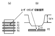
図11は、従来のメモリの冗長回路を用いた救済用フューズの救済前の構造を示す図であり、図11(a)は、上面図、図11(b)は、側面図である。
図12は、従来のメモリの冗長回路を用いた救済用フューズの救済後の構造を示す図であり、図12(a)は、上面図、図12(b)は、側面図である。
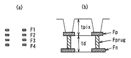
図11、12において、冗長回路用のメモリ救済用フューズF1、F2、F3、F4が図11(a)、図12(a)に示され、この内、救済用フューズF2の構造が、図11(b)、図12(b)に示される。救済用フューズF2上には、フューズ上酸化膜厚tfに酸化膜が形成され、その上にウエハ表面を保護するポリイミド膜厚tpixの保護膜が設けられている。
【0003】
図10において、ウエハは、ウエハプロセスで、レーザートリミングの救済率確保と安定化のため、(1)フューズ上酸化膜エッチングを行い、図11に示されるようにフューズ上酸化膜を所定の膜厚(tf)に調整し、ウエハテスト工程に送られる。ウエハテストでは、まず(2)プリテストを実施し、冗長回路による救済用パターンを決定する。その後、(3)レーザートリミングで、先に決定した救済パターンに従って、図12に示されるように救済用フューズF2の切断を行い、メモリの救済を行う。そして(4)ポストテストで、最終的な良品チップを確認する。その後、バンプ工程に送られ、受入のための(5)エッチングによる表面クリーニング、(6)バンプメッキパターン形成を行った後に、アセンブリ工程で、(7)FC−BGA形成されてパッケージングされ、(8)ファイナルテストを経て良品として完成される(特許文献1参照)。
特許文献2には、ウエハ検査工程の後、フューズ切断工程を経て、パッケージ組立工程に行く記載がある。
【0004】
【特許文献1】
特開2002−319635号公報(第8〜9頁、図6)
【特許文献2】
特開2001−267389号公報(第7〜8頁、図2)
【0005】
【発明が解決しようとする課題】
従来のメモリの救済方法では、効率良く、安定した救済率を得るためには、救済用のフューズ上酸化膜を所定の規格の厚さに調整する必要がある。この場合、後工程であるバンプ工程の(5)表面クリーニング、(6)バンプメッキパターン形成において、このフューズ上酸化膜がエッチングされるため、フューズ上の保護膜でもあるフューズ上酸化膜が消失し、救済したメモリが不良になったり、信頼性上に問題が発生するなどの問題点があった。
また、バンプ工程でのフューズ上酸化膜のエッチング量を想定して、あらかじめ、ウエハプロセス完了時にフューズ上酸化膜厚を最適な膜厚より厚くなるように調整した場合には、レーザートリミングの条件を最適化できないため、救済率の低下や変動が発生し、安定した歩留まりを確保できない問題があった。
【0006】
この発明は、上記のような問題点を解決するためになされたものであり、冗長回路により不良救済を行うことにより、半導体メモリを安定した歩留まりを信頼性を確保して得るようにした半導体メモリの救済方法を得ることを目的としている。
【0007】
【課題を解決するための手段】
この発明に係る半導体メモリの製造方法においては、ウエハ上にフューズを形成する工程、このフューズ上に酸化膜を形成し、所定の膜厚になるようにエッチングする工程、前記エッチングの工程の後に前記ウエハの表面クリーニングを行う工程、前記表面クリーニングを行う工程の後にバンプメッキパターンの形成を行う工程、及び前記バンプメッキパターンの形成を行う工程の後に、ウエハテストにより決定された救済パターンにしたがって前記フューズをレーザートリミングする工程を含み、前記表面クリーニングを行う工程は、前記フューズ上の酸化膜をエッチングする工程により形成される前記酸化膜の膜厚に応じた条件により行われることを特徴とするものである。
【0008】
【発明の実施の形態】
実施の形態1.
図1は、この発明の実施の形態1によるメモリの冗長回路を用いた救済フローを示す図である。
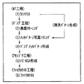
実施の形態1では、ウエハは、ウエハプロセス工程で、レーザートリミングの救済率確保と安定化のため、(1)フューズ上酸化膜エッチングを行い、フューズ上酸化膜を所定の膜厚に調整し、ウエハテスト工程に送られる。ウエハテスト工程において、(2)ウエハテストを実施し、図10の(2)プリテストと同様のメモリ救済パターンを決定する。その後、バンプ工程に送られ、受入のための(3)エッチングによるウエハの表面クリーニング、(4)バンプメッキパターン形成を行った後に、(5)レーザートリミングで、(2)で決定されたメモリ救済パターンに従って、救済用フューズF2の切断を行い、メモリの救済を行う。この際、(1)フューズ上酸化膜エッチングでのフューズ上酸化膜厚は、バンプ工程での表面クリーニングによる減少分を想定して、エッチング量を決定している。そして、アセンブリ工程で(6)FC−BGA(Flip Chip−Ball Glid Array)が形成されてパッケージングされ、ファイナルテスト工程の(7)ファイナルテストを経て、良品として完成される。
【0009】
実施の形態1によれば、バンプメッキ形成後にレーザートリミングを行うようにすることにより、十分な救済率を確保できると共に、フューズ上酸化膜のバンプ工程での消失もなく、信頼性、歩留まりを確保できる効果がある。
【0010】
実施の形態2.
実施の形態2は、図1を援用して説明する。
図1において、実施の形態2では、バンプ工程の(3)表面クリーニングの条件を(1)フューズ上酸化膜エッチングの後のフューズ上酸化膜とフィードバックをかけることにより、(5)レーザートリミングに最適なフューズ上酸化膜厚を調整することを特徴とする。
【0011】
実施の形態2によれば、実施の形態1に対して、より安定して十分な救済率を確保できると共に、フューズ上酸化膜のバンプ工程での消失もなく、信頼性、歩留まりを確保できる効果を得ることができる。
【0012】
実施の形態3.
図2は、この発明の実施の形態3によるメモリの冗長回路を用いた救済フローを示す図である。
図3は、この発明の実施の形態3によるメモリの冗長回路を用いた救済用フューズの救済前の構造を示す図であり、図3(a)は、上面図、図3(b)は、側面図である。図3では、予め切断された状態の救済用フューズを接続することにより救済を行う。
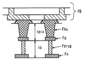
図3において、冗長回路用のメモリ救済用フューズF1、F2、F3、F4が図3(a)に示され、このメモリ救済用フューズF1、F2、F3、F4は、救済前の状態を示し、それぞれ中央部で接続されていない。この救済用フューズFnの構造は、図3(b)に示される。救済用のフューズパッドFpは、コンタクトプラグFprugによって救済フューズパターンとつながれる。救済用フューズFn上には、フューズ上酸化膜厚tdに酸化膜が形成され、その上にウエハ表面を保護するポリイミド膜厚tpixの保護膜が設けられている。
図4は、この発明の実施の形態3によるメモリの冗長回路を用いた救済用フューズの救済後の構造を示す図である。
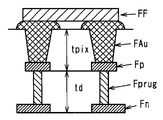
図4において、救済用のバンプ金メッキパターンFAuが、救済用のフューズパッドFp上に形成され、救済用フューズFnを救済した状態を示している。
【0013】
実施の形態3では、図2の(1)ウエハテストで救済パターンを決定後、バンプメッキ工程のメッキパターン形成用の写真製版時にレジストパターンを先に決定した救済パターンに従って、電子ビームなどによる追加露光でトリミングすることで、所望の救済パターンに従ってフューズパッドを結線するようにして、所望の救済用フューズのメタル配線層を接続している。
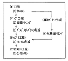
図2においては、ウエハテスト工程において、(1)ウエハテストを実施し、メモリ救済パターンを決定する。その後、バンプ工程に送られ、受入のための(2)エッチングによるウエハの表面クリーニング、(3)メッキパターン写真トリミングにより、メモリ救済パターンにしたがってレジストをトリミングする。(4)レジストを用いてバンプメッキパターン形成を行って、フューズを接続することによりメモリの救済を行う。そして、アセンブリ工程で(5)FC−BGA(Flip Chip−Ball Glid Array)が形成されてパッケージングされ、ファイナルテスト工程の(6)ファイナルテストを経て、良品として完成される。
【0014】
実施の形態3によれば、レーザートリミングによるフューズパターンの切断は不要のため、フューズ上酸化膜のエッチングによる最適膜厚化は不要であり、工程省略の効果があると共に、実施の形態1、2と同様に安定した救済率が得られ、安定した信頼性、歩留まりを確保できる効果を得ることができる。
【0015】
実施の形態4.
図5は、この発明の実施の形態4によるメモリの冗長回路を用いた救済フローを示す図である。
図6は、この発明の実施の形態4によるメモリの冗長回路を用いた救済用フューズの救済後の構造を示す図である。図6では、予め切断された状態の救済用フューズを接続することにより救済を行う。
図6においては、図4の構成である救済用のバンプ金メッキパターンFAuが、救済用のフューズパッドFp上に形成され、これに加えて、救済用の結線チップFFにより、救済用フューズを結線した状態が示されている。
【0016】
実施の形態4では、実施の形態3と同様のフューズパターンを用い、アセンブリ工程において、(1)ウエハテストで決定した救済パターンに応じた救済用のパッド結線チップを組み込むことにより、救済フューズを所望のパターンに結線するように構成している。
図5では、ウエハテスト工程において、(1)ウエハテストを実施し、メモリ救済パターンを決定する。その後、バンプ工程に送られ、受入のための(2)エッチングによるウエハの表面クリーニング、(3)バンプメッキパターン形成を行う。そして、アセンブリ工程で製品として(4)FC−BGA(Flip Chip−Ball Glid Array)形成されてパッケージングされる。このアセンブリ工程で、(6)FC(フリップチップ)基板トリミングを行う。すなわち、救済用のパッド結線チップを用いて救済用フューズを接続することにより、メモリの救済を行う。次いで、ファイナルテスト工程の(5)ファイナルテストを経て、良品として完成される。
【0017】
実施の形態4によれば、実施の形態3と同様にレーザートリミングによるフューズパターンの切断は不要のため、フューズ上酸化膜のエッチングによる最適膜厚化は不要であり、工程省略の効果があると共に、実施の形態1〜3と同様に安定した救済率が得られ、安定した信頼性、歩留まりを確保できる効果を得ることができる。
【0018】
実施の形態5.
実施の形態5は、図5の救済フローと同じである。
図7は、この発明の実施の形態5によるメモリの冗長回路を用いた救済用フューズの救済後の構造を示す図である。図7では、予め切断された状態の救済用フューズを接続することにより救済を行う。
図7において、図4の構成である救済用のバンプ金メッキパターンFAuが、救済用のフューズパッドFp上に形成され、これに加えて、バンプ形成用のプリント基板FBの内部で接続することにより、救済用フューズを結線する。
【0019】
実施の形態4では、フューズ結線用のチップをアセンブリ工程で組み込むようにしていたが、実施の形態5では、チップをバンプアセンブリするプリント基板側で、図5の(1)ウエハテストで決定した救済パターンに従って、フューズパッドを結線するためにプリント基板上に形成されていた配線を、(6)FC基板トリミングにより、レーザートリミングなどによる切断した後に、バンプ金メッキパターンFAuに対応するようにアセンブリすることにより、救済フューズを所望の救済パターンに結線することを特徴としている。
【0020】
実施の形態5によれば、実施の形態3、4と同様にレーザートリミングによるチップ上のフューズパターンの切断は不要のため、フューズ上酸化膜のエッチングによる最適膜厚化は不要であり、工程省略の効果があると共に、実施の形態1〜4と同様に安定した救済率が得られ、安定した信頼性、歩留まりを確保できる効果を得ることができる。
【0021】
実施の形態6.
図8は、この発明の実施の形態6によるメモリの冗長回路を用いた救済フローを示す図である。
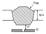
図9は、この発明の実施の形態6によるメモリの冗長回路を用いた救済用フューズの救済後の構造を示す図である。
図9においては、レーザトリミングされた救済用フューズF2上にフューズキャップFcapが設けられている。
実施の形態6は、図10に示された従来のフローとほぼ同じフローにより救済されるが、ウエハテスト工程で、(3)レーザートリミングを実施した後にフューズ上にSOG(Spin On Glass)による保護用のキャップを形成するようにしている。
図8において、ウエハは、ウエハプロセスで、レーザートリミングの救済率確保と安定化のため、(1)フューズ上酸化膜エッチングを行い、フューズ上酸化膜を所定の膜厚に調整し、ウエハテスト工程に送られる。ウエハテストでは、まず(2)プリテストを実施し、冗長回路による救済用パターンを決定する。その後、(3)レーザートリミングで、先に決定した救済パターンに従って、救済用フューズF2の切断を行い、メモリの救済を行う。その後に、SOGによる保護キャップを形成する。そして(4)ポストテストで、最終的な良品チップを確認する。その後、バンプ工程に送られ、受入のための(5)エッチングによる表面クリーニング、(6)バンプメッキパターン形成を行った後に、アセンブリ工程で、(7)FC−BGAが形成されてパッケージングされ、(8)ファイナルテストを経て良品として完成される。
なお、キャップ膜をSOGにより形成すれば、SOGは、パジベーション膜と同じ素材を用いるので、安価で、容易に形成できる利点がある。
【0022】
実施の形態6によれば、フューズ上酸化膜はキャップ膜により保護されているため、バンプ工程において、酸化膜が消失することがないため、図8の(1)フューズ上酸化膜エッチングで、レーザートリミングに最適な膜厚に調整することができるため、実施の形態1〜実施の形態5と同様に安定した救済率が得られ、安定した信頼性、歩留まりを確保できる効果を得ることができる。
【0023】
【発明の効果】
この発明は、以上説明したように、ウエハ上にフューズを形成する工程、このフューズ上に酸化膜を形成し、所定の膜厚になるようにエッチングする工程、前記エッチングの工程の後に前記ウエハの表面クリーニングを行う工程、前記表面クリーニングを行う工程の後にバンプメッキパターンの形成を行う工程、及び前記バンプメッキパターンの形成を行う工程の後に、ウエハテストにより決定された救済パターンにしたがって前記フューズをレーザートリミングする工程を含み、前記表面クリーニングを行う工程は、前記フューズ上の酸化膜をエッチングする工程により形成される前記酸化膜の膜厚に応じた条件により行われるので、バンプ形成のための表面クリーニング後にレーザートリミングを行うようにすることにより、十分な救済率を確保できると共に、フューズ上の酸化膜の表面クリーニングによる消失もなく、信頼性、歩留まりを確保することができる。
【図面の簡単な説明】
【図1】 この発明の実施の形態1、2によるメモリの冗長回路を用いた救済フローを示す図である。
【図2】 この発明の実施の形態3によるメモリの冗長回路を用いた救済フローを示す図である。
【図3】 この発明の実施の形態3によるメモリの冗長回路を用いた救済用フューズの救済前の構造を示す図である。
【図4】 この発明の実施の形態3によるメモリの冗長回路を用いた救済用フューズの救済後の構造を示す図である。
【図5】 この発明の実施の形態4、5によるメモリの冗長回路を用いた救済フローを示す図である。
【図6】 この発明の実施の形態4によるメモリの冗長回路を用いた救済用フューズの救済後の構造を示す図である。
【図7】 この発明の実施の形態5によるメモリの冗長回路を用いた救済用フューズの救済後の構造を示す図である。
【図8】 この発明の実施の形態6によるメモリの冗長回路を用いた救済フローを示す図である。
【図9】 この発明の実施の形態6によるメモリの冗長回路を用いた救済用フューズの救済後の構造を示す図である。
【図10】 従来のメモリの冗長回路を用いた救済フローを示す図である。
【図11】 従来のメモリの冗長回路を用いた救済用フューズの救済前の構造を示す図である。
【図12】 従来のメモリの冗長回路を用いた救済用フューズの救済後の構造を示す図である。
【符号の説明】
F1,F2,F3,F4,Fn 冗長回路用のメモリ救済用フューズ、
Fp 救済用のフューズパッド、Fprug コンタクトプラグ、
td フューズ上酸化膜厚、tpix ポリイミド膜厚、
FAu 救済用のバンプ金メッキパターン、FF 救済用の結線チップ、
FB バンプ形成用の基板、Fcap フューズキャップ。[0001]
BACKGROUND OF THE INVENTION
The present invention relates to a semiconductor memory device and a semiconductor memory repair method for performing repair by a redundant circuit of a memory formed in an integrated circuit.
[0002]
[Prior art]
FIG. 10 is a diagram showing a relief flow using a conventional memory redundancy circuit.
11A and 11B are diagrams showing a structure before a relief fuse using a redundancy circuit of a conventional memory, in which FIG. 11A is a top view and FIG. 11B is a side view.
12A and 12B are diagrams showing a structure after a relief fuse using a redundancy circuit of a conventional memory, in which FIG. 12A is a top view and FIG. 12B is a side view.
11 and 12, memory relief fuses F1, F2, F3, and F4 for redundant circuits are shown in FIGS. 11A and 12A, and the structure of the relief fuse F2 is shown in FIG. (B) is shown in FIG. On the relief fuse F2, an oxide film is formed on the oxide film thickness tf on the fuse, and a protective film having a polyimide film thickness tpix for protecting the wafer surface is provided thereon.
[0003]
In FIG. 10, the wafer is processed in a wafer process in order to ensure and stabilize the laser trimming relief rate. (1) Oxide oxide film etching is performed, and as shown in FIG. Adjust to (tf) and send to wafer test process. In the wafer test, first, (2) a pretest is performed to determine a repair pattern by a redundant circuit. Thereafter, (3) laser trimming is performed to cut the relief fuse F2 as shown in FIG. 12 according to the relief pattern determined in advance, and the memory is rescued. (4) The final non-defective chip is confirmed by a post test. Then, it is sent to the bump process, and after receiving (5) surface cleaning by etching and (6) bump plating pattern formation, (7) FC-BGA is formed and packaged in the assembly process. 8) Completed as a non-defective product through a final test (see Patent Document 1).
Patent Document 2 describes that after the wafer inspection process, a fuse cutting process is performed and then a package assembly process is performed.
[0004]
[Patent Document 1]
JP 2002-319635 A (pages 8-9, FIG. 6)
[Patent Document 2]
JP 2001-267389 A (7th to 8th pages, FIG. 2)
[0005]
[Problems to be solved by the invention]
In the conventional memory repair method, in order to obtain an efficient and stable repair rate, it is necessary to adjust the oxide film on the fuse for repair to a predetermined standard thickness. In this case, since the oxide film on the fuse is etched in (5) surface cleaning and (6) bump plating pattern formation in the subsequent bump process, the oxide film on the fuse which is also a protective film on the fuse disappears. However, there are problems such as defective repaired memory and problems in reliability.
Assuming the etching amount of the oxide film on the fuse in the bump process, if the oxide film thickness on the fuse is adjusted in advance to be thicker than the optimum film thickness when the wafer process is completed, the laser trimming conditions are set. Since the optimization cannot be performed, there is a problem that the repair rate is lowered or fluctuated and a stable yield cannot be secured.
[0006]
The present invention has been made in order to solve the above-described problems, and a semiconductor memory in which a semiconductor memory can be obtained with a stable yield while ensuring reliability by performing defect repair using a redundant circuit. The purpose is to obtain a remedy.
[0007]
[Means for Solving the Problems]
In the method of manufacturing a semiconductor memory according to the present invention, a step of forming a fuse on a wafer, a step of forming an oxide film on the fuse, etching to a predetermined thickness, and the step after the etching step A fuse surface according to a relief pattern determined by a wafer test after a wafer surface cleaning step, a bump plating pattern formation step after the surface cleaning step, and a bump plating pattern formation step; look including the step of laser trimming the step of performing the surface cleaning, which comprises carrying out the conditions where the corresponding to the thickness of the oxide film formed by etching the oxide film on the fuse It is.
[0008]
DETAILED DESCRIPTION OF THE INVENTION
Embodiment 1 FIG.
FIG. 1 is a diagram showing a relief flow using a memory redundancy circuit according to the first embodiment of the present invention.
In the first embodiment, in order to secure and stabilize the laser trimming relief rate in the wafer process step, the wafer is processed by (1) etching the oxide film on the fuse, adjusting the oxide film on the fuse to a predetermined film thickness, It is sent to the wafer test process. In the wafer test process, (2) a wafer test is performed, and a memory relief pattern similar to (2) pretest in FIG. 10 is determined. Then, it is sent to the bump process, and after receiving (3) wafer surface cleaning by etching and (4) bump plating pattern formation, (5) laser trimming and memory relief determined in (2) According to the pattern, the relief fuse F2 is cut and the memory is rescued. At this time, (1) the oxide film thickness on the fuse in the oxide film etching on the fuse is determined in consideration of the decrease due to the surface cleaning in the bump process. Then, (6) FC-BGA (Flip Chip-Ball Glid Array) is formed and packaged in the assembly process, and is completed as a non-defective product through (7) final test in the final test process.
[0009]
According to the first embodiment, by performing laser trimming after the bump plating is formed, a sufficient relief rate can be ensured, and the reliability and yield can be ensured without loss of the oxide film on the fuse in the bump process. There is an effect that can be done.
[0010]
Embodiment 2. FIG.
The second embodiment will be described with reference to FIG.
In FIG. 1, in the second embodiment, the (3) surface cleaning conditions in the bump process are fed back to (1) the oxide film on the fuse after the oxide film etching on the fuse, and (5) optimum for laser trimming. It is characterized by adjusting the oxide thickness on the fuse.
[0011]
According to the second embodiment, a sufficient relief rate can be secured more stably than the first embodiment, and the reliability and yield can be secured without loss in the bump process of the oxide film on the fuse. Can be obtained.
[0012]
Embodiment 3 FIG.
FIG. 2 is a diagram showing a repair flow using the memory redundancy circuit according to the third embodiment of the present invention.
FIGS. 3A and 3B are diagrams showing a structure before repair of the repair fuse using the memory redundancy circuit according to the third embodiment of the present invention. FIG. 3A is a top view and FIG. It is a side view. In FIG. 3, relief is performed by connecting a relief fuse that has been cut in advance.
In FIG. 3, memory relief fuses F1, F2, F3, and F4 for redundant circuits are shown in FIG. 3A, and the memory relief fuses F1, F2, F3, and F4 indicate the state before the relief, They are not connected at the center. The structure of this relief fuse Fn is shown in FIG. The relief fuse pad Fp is connected to the relief fuse pattern by the contact plug Fprug. On the relief fuse Fn, an oxide film is formed with an oxide film thickness td on the fuse, and a protective film with a polyimide film thickness tpix for protecting the wafer surface is provided thereon.
FIG. 4 is a diagram showing the structure after repair of the repair fuse using the memory redundancy circuit according to the third embodiment of the present invention.
FIG. 4 shows a state where the relief bump gold plating pattern FAu is formed on the relief fuse pad Fp and the relief fuse Fn is rescued.
[0013]
In the third embodiment, after the relief pattern is determined by (1) wafer test in FIG. 2, additional exposure using an electron beam or the like is performed according to the relief pattern previously determined at the time of photoengraving for plating pattern formation in the bump plating process. By trimming in this manner, the metal pads of the desired relief fuse are connected so that the fuse pads are connected according to the desired relief pattern.
In FIG. 2, in the wafer test process, (1) a wafer test is performed and a memory relief pattern is determined. Thereafter, the resist is trimmed according to the memory relief pattern by (2) wafer surface cleaning by etching and (3) plating pattern photo trimming for acceptance, which is sent to a bump process. (4) A bump plating pattern is formed using a resist, and a memory is relieved by connecting a fuse. Then, (5) FC-BGA (Flip Chip-Ball Glid Array) is formed and packaged in the assembly process, and is completed as a non-defective product through (6) final test in the final test process.
[0014]
According to the third embodiment, since it is unnecessary to cut the fuse pattern by laser trimming, there is no need to optimize the film thickness by etching the oxide film on the fuse. In the same manner as described above, a stable relief rate can be obtained, and an effect of ensuring stable reliability and yield can be obtained.
[0015]
Embodiment 4 FIG.
FIG. 5 is a diagram showing a repair flow using the memory redundancy circuit according to the fourth embodiment of the present invention.
FIG. 6 is a diagram showing the structure after repair of the repair fuse using the memory redundancy circuit according to the fourth embodiment of the present invention. In FIG. 6, relief is performed by connecting a relief fuse that has been cut in advance.
In FIG. 6, the relief bump gold plating pattern FAu having the configuration of FIG. 4 is formed on the relief fuse pad Fp, and in addition, the relief fuse is connected by the relief connection chip FF. The state is shown.
[0016]
In the fourth embodiment, the same fuse pattern as in the third embodiment is used, and in the assembly process, a relief fuse is desired by incorporating a relief pad connection chip corresponding to the relief pattern determined in the wafer test (1). It is configured to connect to the pattern.
In FIG. 5, in the wafer test process, (1) a wafer test is performed and a memory relief pattern is determined. Then, it is sent to a bump process, and (2) wafer surface cleaning by etching and (3) bump plating pattern formation for acceptance are performed. Then, (4) FC-BGA (Flip Chip-Ball Glid Array) is formed and packaged as a product in the assembly process. In this assembly process, (6) FC (flip chip) substrate trimming is performed. That is, the memory is relieved by connecting a relief fuse using a relief pad connection chip. Next, after a final test (5) final test, it is completed as a non-defective product.
[0017]
According to the fourth embodiment, as in the third embodiment, since cutting of the fuse pattern by laser trimming is not necessary, the optimum film thickness by etching of the oxide film on the fuse is unnecessary, and there is an effect of omitting the process. As in the first to third embodiments, a stable relief rate can be obtained, and an effect of ensuring stable reliability and yield can be obtained.
[0018]
Embodiment 5 FIG.
The fifth embodiment is the same as the relief flow of FIG.
FIG. 7 is a diagram showing the structure after repair of the repair fuse using the memory redundancy circuit according to the fifth embodiment of the present invention. In FIG. 7, relief is performed by connecting a relief fuse that has been cut in advance.
In FIG. 7, the relief bump gold plating pattern FAu having the configuration of FIG. 4 is formed on the relief fuse pad Fp, and in addition, by connecting inside the bump forming printed circuit board FB, Connect the relief fuse.
[0019]
In the fourth embodiment, the chip for fuse connection is incorporated in the assembly process, but in the fifth embodiment, the relief determined by (1) wafer test in FIG. 5 on the printed circuit board side where the chip is bump-assembled. According to the pattern, the wiring formed on the printed circuit board for connecting the fuse pads is (6) cut by FC board trimming by laser trimming, etc., and then assembled so as to correspond to the bump gold plating pattern FAu The relief fuse is connected to a desired relief pattern.
[0020]
According to the fifth embodiment, since the fuse pattern on the chip is not cut by laser trimming as in the third and fourth embodiments, the optimum film thickness by etching of the oxide film on the fuse is unnecessary, and the process is omitted. In addition to the above effects, a stable relief rate can be obtained in the same manner as in the first to fourth embodiments, and an effect of ensuring stable reliability and yield can be obtained.
[0021]
Embodiment 6 FIG.
FIG. 8 is a diagram showing a relief flow using the memory redundancy circuit according to the sixth embodiment of the present invention.
FIG. 9 shows a structure after repair of the repair fuse using the memory redundancy circuit according to the sixth embodiment of the present invention.
In FIG. 9, a fuse cap Fcap is provided on the laser trimmed relief fuse F2.
The sixth embodiment is relieved by almost the same flow as the conventional flow shown in FIG. 10, but in the wafer test process, (3) protection by SOG (Spin On Glass) on the fuse after performing laser trimming. A cap is formed.
In FIG. 8, in order to secure and stabilize the laser trimming relief rate in the wafer process, the wafer is processed by (1) etching the oxide film on the fuse, adjusting the oxide film on the fuse to a predetermined film thickness, and performing a wafer test process. Sent to. In the wafer test, first, (2) a pretest is performed to determine a repair pattern by a redundant circuit. Thereafter, in (3) laser trimming, the relief fuse F2 is cut in accordance with the relief pattern determined earlier, and the memory is rescued. Thereafter, a protective cap made of SOG is formed. (4) The final non-defective chip is confirmed by a post test. After that, it was sent to the bump process, and after receiving (5) surface cleaning by etching and (6) bump plating pattern formation, (7) FC-BGA was formed and packaged in the assembly process, (8) Completed as a non-defective product through a final test.
If the cap film is formed of SOG, SOG uses the same material as that of the passivation film, so that there is an advantage that it can be easily formed at low cost.
[0022]
According to the sixth embodiment, since the oxide film on the fuse is protected by the cap film, the oxide film is not lost in the bump process. Therefore, in (1) oxide film etching on the fuse shown in FIG. Since the film thickness can be adjusted to be optimal for trimming, a stable relief rate can be obtained as in the first to fifth embodiments, and an effect of ensuring stable reliability and yield can be obtained.
[0023]
【The invention's effect】
As described above, the present invention includes a step of forming a fuse on a wafer, a step of forming an oxide film on the fuse and etching to a predetermined thickness, and a step of forming the wafer after the etching step. After the surface cleaning step, the surface cleaning step, the bump plating pattern formation step, and the bump plating pattern formation step, the fuse is lasered according to a relief pattern determined by a wafer test. look including the step of trimming, the step of performing the surface cleaning, since carried out according to the conditions the corresponding to the thickness of the oxide film formed by etching the oxide film on the fuse, the surface for the bump formation Sufficient relief by doing laser trimming after cleaning The can be ensured, without loss due to surface cleaning of the oxide film on the fuse, it is possible to ensure reliability, the yield.
[Brief description of the drawings]
FIG. 1 is a diagram showing a relief flow using a memory redundancy circuit according to first and second embodiments of the present invention;
FIG. 2 is a diagram showing a relief flow using a memory redundancy circuit according to a third embodiment of the present invention.
FIG. 3 is a diagram showing a structure before repair of a repair fuse using a memory redundant circuit according to a third embodiment of the present invention;
FIG. 4 is a diagram showing a structure after repair of a repair fuse using a memory redundancy circuit according to Embodiment 3 of the present invention;
FIG. 5 is a diagram showing a relief flow using a memory redundancy circuit according to Embodiments 4 and 5 of the present invention;
FIG. 6 is a diagram showing a structure after repair of a repair fuse using a memory redundancy circuit according to Embodiment 4 of the present invention;
FIG. 7 is a diagram showing a structure after repair of a repair fuse using a memory redundant circuit according to a fifth embodiment of the present invention;
FIG. 8 is a diagram showing a relief flow using a memory redundancy circuit according to a sixth embodiment of the present invention.
FIG. 9 is a diagram showing a structure after repair of a repair fuse using a memory redundant circuit according to a sixth embodiment of the present invention;
FIG. 10 is a diagram showing a relief flow using a conventional memory redundancy circuit;
FIG. 11 is a diagram showing a structure before repair of a repair fuse using a redundancy circuit of a conventional memory.
FIG. 12 is a diagram showing a structure after relief of a relief fuse using a conventional memory redundancy circuit;
[Explanation of symbols]
F1, F2, F3, F4, Fn Memory relief fuse for redundant circuit,
Fp relief fuse pad, Fprug contact plug,
td oxide thickness on fuse, tpix polyimide film thickness,
Fau relief bump gold plating pattern, FF relief connection chip,
FB Substrate for bump formation, FCap fuse cap.
Claims (1)
前記表面クリーニングを行う工程は、前記フューズ上の酸化膜をエッチングする工程により形成される前記酸化膜の膜厚に応じた条件により行われることを特徴とする半導体メモリの製造方法。A step of forming a fuse on the wafer, a step of forming an oxide film on the fuse and etching the film to a predetermined thickness, a step of cleaning the surface of the wafer after the etching step, and the surface cleaning. step effect formation of bump plating pattern after the step of performing, and after the step of performing the formation of the bump plating pattern, viewed including the step of laser trimming the fuse according to the relief pattern determined by the wafer test,
The method of manufacturing a semiconductor memory, wherein the surface cleaning step is performed under conditions according to a thickness of the oxide film formed by the step of etching the oxide film on the fuse .
Priority Applications (1)
| Application Number | Priority Date | Filing Date | Title |
|---|---|---|---|
| JP2003128516A JP4236509B2 (en) | 2003-05-07 | 2003-05-07 | Manufacturing method of semiconductor memory |
Applications Claiming Priority (1)
| Application Number | Priority Date | Filing Date | Title |
|---|---|---|---|
| JP2003128516A JP4236509B2 (en) | 2003-05-07 | 2003-05-07 | Manufacturing method of semiconductor memory |
Publications (3)
| Publication Number | Publication Date |
|---|---|
| JP2004335672A JP2004335672A (en) | 2004-11-25 |
| JP2004335672A5 JP2004335672A5 (en) | 2006-06-22 |
| JP4236509B2 true JP4236509B2 (en) | 2009-03-11 |
Family
ID=33504609
Family Applications (1)
| Application Number | Title | Priority Date | Filing Date |
|---|---|---|---|
| JP2003128516A Expired - Fee Related JP4236509B2 (en) | 2003-05-07 | 2003-05-07 | Manufacturing method of semiconductor memory |
Country Status (1)
| Country | Link |
|---|---|
| JP (1) | JP4236509B2 (en) |
Families Citing this family (1)
| Publication number | Priority date | Publication date | Assignee | Title |
|---|---|---|---|---|
| JP2009062317A (en) * | 2007-09-06 | 2009-03-26 | Nissan Chem Ind Ltd | Photochromic material and optical recording medium using thiophene derivative |
-
2003
- 2003-05-07 JP JP2003128516A patent/JP4236509B2/en not_active Expired - Fee Related
Also Published As
| Publication number | Publication date |
|---|---|
| JP2004335672A (en) | 2004-11-25 |
Similar Documents
| Publication | Publication Date | Title |
|---|---|---|
| US4602420A (en) | Method of manufacturing a semiconductor device | |
| JP4068838B2 (en) | Manufacturing method of semiconductor device | |
| KR100385225B1 (en) | Flip chip type semiconductor device having probing pads and bump pads and fabrication method thereof | |
| KR100907351B1 (en) | Semiconductor integrated circuit device and method of manufacturing the same | |
| US9397054B2 (en) | Semiconductor structure with an interconnect level having a conductive pad and metallic structure such as a base of a crackstop | |
| CN101414584A (en) | Semiconductor device and method of fabricating semiconductor device | |
| JP4601910B2 (en) | Semiconductor integrated circuit device and manufacturing method of semiconductor integrated circuit device | |
| US5946597A (en) | Semiconductor chip mounting method | |
| US6579734B2 (en) | Wire bonding method | |
| US7666734B2 (en) | Semiconductor device having a fuse | |
| JP4072141B2 (en) | Manufacturing method of semiconductor device | |
| JP4236509B2 (en) | Manufacturing method of semiconductor memory | |
| CN101114609B (en) | Manufacturing method of fuse box with vertically formed protective film | |
| KR100556351B1 (en) | Metal pad and metal pad bonding method of semiconductor device | |
| JP3506369B2 (en) | Semiconductor integrated circuit device and manufacturing method thereof | |
| US7517786B2 (en) | Methods of forming wire bonds for semiconductor constructions | |
| US20060030082A1 (en) | Semiconductor device and fabricating method thereof | |
| JP2001189424A (en) | Semiconductor device and method of manufacturing the same | |
| JPH05136271A (en) | Semiconductor integrated circuit device and manufacturing method thereof | |
| JPH02215149A (en) | Semiconductor device and its manufacture | |
| JPH02184063A (en) | Semiconductor device and manufacture thereof | |
| JP2003092353A (en) | Semiconductor device and manufacturing method thereof | |
| JP4401092B2 (en) | Method for manufacturing signal transmission circuit and method for manufacturing semiconductor circuit | |
| KR100833588B1 (en) | Manufacturing method of semiconductor device | |
| KR20010064720A (en) | Semiconductor device having improved scribe line and manufacturing method thereof |
Legal Events
| Date | Code | Title | Description |
|---|---|---|---|
| RD01 | Notification of change of attorney |
Free format text: JAPANESE INTERMEDIATE CODE: A7421 Effective date: 20060123 |
|
| A521 | Written amendment |
Free format text: JAPANESE INTERMEDIATE CODE: A523 Effective date: 20060502 |
|
| A621 | Written request for application examination |
Free format text: JAPANESE INTERMEDIATE CODE: A621 Effective date: 20060502 |
|
| RD01 | Notification of change of attorney |
Free format text: JAPANESE INTERMEDIATE CODE: A7421 Effective date: 20071101 |
|
| A977 | Report on retrieval |
Free format text: JAPANESE INTERMEDIATE CODE: A971007 Effective date: 20080925 |
|
| A131 | Notification of reasons for refusal |
Free format text: JAPANESE INTERMEDIATE CODE: A131 Effective date: 20080930 |
|
| A521 | Written amendment |
Free format text: JAPANESE INTERMEDIATE CODE: A523 Effective date: 20081113 |
|
| TRDD | Decision of grant or rejection written | ||
| A01 | Written decision to grant a patent or to grant a registration (utility model) |
Free format text: JAPANESE INTERMEDIATE CODE: A01 Effective date: 20081209 |
|
| A01 | Written decision to grant a patent or to grant a registration (utility model) |
Free format text: JAPANESE INTERMEDIATE CODE: A01 |
|
| A61 | First payment of annual fees (during grant procedure) |
Free format text: JAPANESE INTERMEDIATE CODE: A61 Effective date: 20081216 |
|
| R150 | Certificate of patent or registration of utility model |
Free format text: JAPANESE INTERMEDIATE CODE: R150 |
|
| FPAY | Renewal fee payment (event date is renewal date of database) |
Free format text: PAYMENT UNTIL: 20111226 Year of fee payment: 3 |
|
| FPAY | Renewal fee payment (event date is renewal date of database) |
Free format text: PAYMENT UNTIL: 20111226 Year of fee payment: 3 |
|
| S111 | Request for change of ownership or part of ownership |
Free format text: JAPANESE INTERMEDIATE CODE: R313111 |
|
| FPAY | Renewal fee payment (event date is renewal date of database) |
Free format text: PAYMENT UNTIL: 20111226 Year of fee payment: 3 |
|
| R350 | Written notification of registration of transfer |
Free format text: JAPANESE INTERMEDIATE CODE: R350 |
|
| FPAY | Renewal fee payment (event date is renewal date of database) |
Free format text: PAYMENT UNTIL: 20111226 Year of fee payment: 3 |
|
| FPAY | Renewal fee payment (event date is renewal date of database) |
Free format text: PAYMENT UNTIL: 20121226 Year of fee payment: 4 |
|
| FPAY | Renewal fee payment (event date is renewal date of database) |
Free format text: PAYMENT UNTIL: 20121226 Year of fee payment: 4 |
|
| FPAY | Renewal fee payment (event date is renewal date of database) |
Free format text: PAYMENT UNTIL: 20131226 Year of fee payment: 5 |
|
| LAPS | Cancellation because of no payment of annual fees |