JP4236440B2 - IC card - Google Patents
IC card Download PDFInfo
- Publication number
- JP4236440B2 JP4236440B2 JP2002296472A JP2002296472A JP4236440B2 JP 4236440 B2 JP4236440 B2 JP 4236440B2 JP 2002296472 A JP2002296472 A JP 2002296472A JP 2002296472 A JP2002296472 A JP 2002296472A JP 4236440 B2 JP4236440 B2 JP 4236440B2
- Authority
- JP
- Japan
- Prior art keywords
- card
- controller
- mmc
- adapter
- terminal
- Prior art date
- Legal status (The legal status is an assumption and is not a legal conclusion. Google has not performed a legal analysis and makes no representation as to the accuracy of the status listed.)
- Expired - Fee Related
Links
Images


Classifications
-
- G—PHYSICS
- G06—COMPUTING; CALCULATING OR COUNTING
- G06K—GRAPHICAL DATA READING; PRESENTATION OF DATA; RECORD CARRIERS; HANDLING RECORD CARRIERS
- G06K19/00—Record carriers for use with machines and with at least a part designed to carry digital markings
- G06K19/06—Record carriers for use with machines and with at least a part designed to carry digital markings characterised by the kind of the digital marking, e.g. shape, nature, code
- G06K19/067—Record carriers with conductive marks, printed circuits or semiconductor circuit elements, e.g. credit or identity cards also with resonating or responding marks without active components
- G06K19/07—Record carriers with conductive marks, printed circuits or semiconductor circuit elements, e.g. credit or identity cards also with resonating or responding marks without active components with integrated circuit chips
- G06K19/077—Constructional details, e.g. mounting of circuits in the carrier
- G06K19/0772—Physical layout of the record carrier
- G06K19/07732—Physical layout of the record carrier the record carrier having a housing or construction similar to well-known portable memory devices, such as SD cards, USB or memory sticks
-
- G—PHYSICS
- G06—COMPUTING; CALCULATING OR COUNTING
- G06K—GRAPHICAL DATA READING; PRESENTATION OF DATA; RECORD CARRIERS; HANDLING RECORD CARRIERS
- G06K17/00—Methods or arrangements for effecting co-operative working between equipments covered by two or more of main groups G06K1/00 - G06K15/00, e.g. automatic card files incorporating conveying and reading operations
-
- G—PHYSICS
- G06—COMPUTING; CALCULATING OR COUNTING
- G06K—GRAPHICAL DATA READING; PRESENTATION OF DATA; RECORD CARRIERS; HANDLING RECORD CARRIERS
- G06K19/00—Record carriers for use with machines and with at least a part designed to carry digital markings
- G06K19/06—Record carriers for use with machines and with at least a part designed to carry digital markings characterised by the kind of the digital marking, e.g. shape, nature, code
- G06K19/067—Record carriers with conductive marks, printed circuits or semiconductor circuit elements, e.g. credit or identity cards also with resonating or responding marks without active components
- G06K19/07—Record carriers with conductive marks, printed circuits or semiconductor circuit elements, e.g. credit or identity cards also with resonating or responding marks without active components with integrated circuit chips
- G06K19/0719—Record carriers with conductive marks, printed circuits or semiconductor circuit elements, e.g. credit or identity cards also with resonating or responding marks without active components with integrated circuit chips at least one of the integrated circuit chips comprising an arrangement for application selection, e.g. an acceleration sensor or a set of radio buttons
-
- G—PHYSICS
- G06—COMPUTING; CALCULATING OR COUNTING
- G06K—GRAPHICAL DATA READING; PRESENTATION OF DATA; RECORD CARRIERS; HANDLING RECORD CARRIERS
- G06K19/00—Record carriers for use with machines and with at least a part designed to carry digital markings
- G06K19/06—Record carriers for use with machines and with at least a part designed to carry digital markings characterised by the kind of the digital marking, e.g. shape, nature, code
- G06K19/067—Record carriers with conductive marks, printed circuits or semiconductor circuit elements, e.g. credit or identity cards also with resonating or responding marks without active components
- G06K19/07—Record carriers with conductive marks, printed circuits or semiconductor circuit elements, e.g. credit or identity cards also with resonating or responding marks without active components with integrated circuit chips
- G06K19/077—Constructional details, e.g. mounting of circuits in the carrier
- G06K19/0772—Physical layout of the record carrier
- G06K19/07733—Physical layout of the record carrier the record carrier containing at least one further contact interface not conform ISO-7816
-
- G—PHYSICS
- G06—COMPUTING; CALCULATING OR COUNTING
- G06K—GRAPHICAL DATA READING; PRESENTATION OF DATA; RECORD CARRIERS; HANDLING RECORD CARRIERS
- G06K19/00—Record carriers for use with machines and with at least a part designed to carry digital markings
- G06K19/06—Record carriers for use with machines and with at least a part designed to carry digital markings characterised by the kind of the digital marking, e.g. shape, nature, code
- G06K19/067—Record carriers with conductive marks, printed circuits or semiconductor circuit elements, e.g. credit or identity cards also with resonating or responding marks without active components
- G06K19/07—Record carriers with conductive marks, printed circuits or semiconductor circuit elements, e.g. credit or identity cards also with resonating or responding marks without active components with integrated circuit chips
- G06K19/077—Constructional details, e.g. mounting of circuits in the carrier
- G06K19/07737—Constructional details, e.g. mounting of circuits in the carrier the record carrier consisting of two or more mechanically separable parts
- G06K19/07741—Constructional details, e.g. mounting of circuits in the carrier the record carrier consisting of two or more mechanically separable parts comprising a first part operating as a regular record carrier and a second attachable part that changes the functional appearance of said record carrier, e.g. a contact-based smart card with an adapter part which, when attached to the contact card makes the contact card function as a non-contact card
-
- G—PHYSICS
- G06—COMPUTING; CALCULATING OR COUNTING
- G06K—GRAPHICAL DATA READING; PRESENTATION OF DATA; RECORD CARRIERS; HANDLING RECORD CARRIERS
- G06K19/00—Record carriers for use with machines and with at least a part designed to carry digital markings
- G06K19/06—Record carriers for use with machines and with at least a part designed to carry digital markings characterised by the kind of the digital marking, e.g. shape, nature, code
- G06K19/067—Record carriers with conductive marks, printed circuits or semiconductor circuit elements, e.g. credit or identity cards also with resonating or responding marks without active components
- G06K19/07—Record carriers with conductive marks, printed circuits or semiconductor circuit elements, e.g. credit or identity cards also with resonating or responding marks without active components with integrated circuit chips
- G06K19/077—Constructional details, e.g. mounting of circuits in the carrier
- G06K19/07743—External electrical contacts
-
- H—ELECTRICITY
- H01—ELECTRIC ELEMENTS
- H01L—SEMICONDUCTOR DEVICES NOT COVERED BY CLASS H10
- H01L2224/00—Indexing scheme for arrangements for connecting or disconnecting semiconductor or solid-state bodies and methods related thereto as covered by H01L24/00
- H01L2224/01—Means for bonding being attached to, or being formed on, the surface to be connected, e.g. chip-to-package, die-attach, "first-level" interconnects; Manufacturing methods related thereto
- H01L2224/42—Wire connectors; Manufacturing methods related thereto
- H01L2224/44—Structure, shape, material or disposition of the wire connectors prior to the connecting process
- H01L2224/45—Structure, shape, material or disposition of the wire connectors prior to the connecting process of an individual wire connector
- H01L2224/45001—Core members of the connector
- H01L2224/45099—Material
- H01L2224/451—Material with a principal constituent of the material being a metal or a metalloid, e.g. boron (B), silicon (Si), germanium (Ge), arsenic (As), antimony (Sb), tellurium (Te) and polonium (Po), and alloys thereof
- H01L2224/45138—Material with a principal constituent of the material being a metal or a metalloid, e.g. boron (B), silicon (Si), germanium (Ge), arsenic (As), antimony (Sb), tellurium (Te) and polonium (Po), and alloys thereof the principal constituent melting at a temperature of greater than or equal to 950°C and less than 1550°C
- H01L2224/45144—Gold (Au) as principal constituent
-
- H—ELECTRICITY
- H01—ELECTRIC ELEMENTS
- H01L—SEMICONDUCTOR DEVICES NOT COVERED BY CLASS H10
- H01L2224/00—Indexing scheme for arrangements for connecting or disconnecting semiconductor or solid-state bodies and methods related thereto as covered by H01L24/00
- H01L2224/01—Means for bonding being attached to, or being formed on, the surface to be connected, e.g. chip-to-package, die-attach, "first-level" interconnects; Manufacturing methods related thereto
- H01L2224/42—Wire connectors; Manufacturing methods related thereto
- H01L2224/47—Structure, shape, material or disposition of the wire connectors after the connecting process
- H01L2224/48—Structure, shape, material or disposition of the wire connectors after the connecting process of an individual wire connector
- H01L2224/4805—Shape
- H01L2224/4809—Loop shape
- H01L2224/48091—Arched
-
- H—ELECTRICITY
- H01—ELECTRIC ELEMENTS
- H01L—SEMICONDUCTOR DEVICES NOT COVERED BY CLASS H10
- H01L2224/00—Indexing scheme for arrangements for connecting or disconnecting semiconductor or solid-state bodies and methods related thereto as covered by H01L24/00
- H01L2224/01—Means for bonding being attached to, or being formed on, the surface to be connected, e.g. chip-to-package, die-attach, "first-level" interconnects; Manufacturing methods related thereto
- H01L2224/42—Wire connectors; Manufacturing methods related thereto
- H01L2224/47—Structure, shape, material or disposition of the wire connectors after the connecting process
- H01L2224/48—Structure, shape, material or disposition of the wire connectors after the connecting process of an individual wire connector
- H01L2224/481—Disposition
- H01L2224/48151—Connecting between a semiconductor or solid-state body and an item not being a semiconductor or solid-state body, e.g. chip-to-substrate, chip-to-passive
- H01L2224/48221—Connecting between a semiconductor or solid-state body and an item not being a semiconductor or solid-state body, e.g. chip-to-substrate, chip-to-passive the body and the item being stacked
- H01L2224/48225—Connecting between a semiconductor or solid-state body and an item not being a semiconductor or solid-state body, e.g. chip-to-substrate, chip-to-passive the body and the item being stacked the item being non-metallic, e.g. insulating substrate with or without metallisation
- H01L2224/48227—Connecting between a semiconductor or solid-state body and an item not being a semiconductor or solid-state body, e.g. chip-to-substrate, chip-to-passive the body and the item being stacked the item being non-metallic, e.g. insulating substrate with or without metallisation connecting the wire to a bond pad of the item
-
- H—ELECTRICITY
- H05—ELECTRIC TECHNIQUES NOT OTHERWISE PROVIDED FOR
- H05K—PRINTED CIRCUITS; CASINGS OR CONSTRUCTIONAL DETAILS OF ELECTRIC APPARATUS; MANUFACTURE OF ASSEMBLAGES OF ELECTRICAL COMPONENTS
- H05K1/00—Printed circuits
- H05K1/02—Details
- H05K1/0266—Marks, test patterns or identification means
- H05K1/0268—Marks, test patterns or identification means for electrical inspection or testing
-
- H—ELECTRICITY
- H05—ELECTRIC TECHNIQUES NOT OTHERWISE PROVIDED FOR
- H05K—PRINTED CIRCUITS; CASINGS OR CONSTRUCTIONAL DETAILS OF ELECTRIC APPARATUS; MANUFACTURE OF ASSEMBLAGES OF ELECTRICAL COMPONENTS
- H05K1/00—Printed circuits
- H05K1/02—Details
- H05K1/11—Printed elements for providing electric connections to or between printed circuits
- H05K1/117—Pads along the edge of rigid circuit boards, e.g. for pluggable connectors
Landscapes
- Engineering & Computer Science (AREA)
- Computer Hardware Design (AREA)
- Microelectronics & Electronic Packaging (AREA)
- Physics & Mathematics (AREA)
- General Physics & Mathematics (AREA)
- Theoretical Computer Science (AREA)
- Credit Cards Or The Like (AREA)
Description
【0001】
【発明の属する技術分野】
本発明は、ICカードおよびアダプタに関し、特に、特定のICカードを種々の形状、ピン(外部端子)数、特性を有する他のICカードとして使用する際に用いて有効な技術に関する。
【0002】
【従来の技術】
小型メモリカードとして、電気的書き込みおよび消去が可能な不揮発性メモリ(フラッシュEEPROM:Electrically Erasable Programmable Read Only Memory)を搭載した切手程度の大きさのメモリカードの開発が進められている。
【0003】
このような小型メモリカードは、デジタルカメラや携帯電話などの小型機器の記憶媒体として既に実用化されているものも多い。
【0004】
しかしながら、このような小型メモリカードの規格(外形寸法やピン数、内部機能等)は複数あり、相互に互換性を有さない規格も存在する。図46に、小型メモリカードの規格の一例として開発企業と商品名およびその外形寸法などを示す。
【0005】
例えば、下記特許文献1(特開平7−141114号公報)には、メモリカード3aを装着した状態のアダプタ30を情報機器22のメモリカードスロット21に挿入することにより、情報機器22とメモリカード3aとの間における情報信号の送受信をシリアルデータで行えるようにした技術が開示されている(図10参照)。
【0006】
また、下記特許文献2(特開2001−307801号公報)には、SDカード50が着脱されるSDカードコネクタ部10と、SIMカード60が着脱されるSIMカードコネクタ部20とを上下一体不可分に樹脂で成型したメモリカード用コネクタが開示されている(図2参照)。
【0007】
【特許文献1】
特開平7−141114号公報、要約および図10参照
【0008】
【特許文献2】
特開2001−307801号公報、要約および図2参照
【0009】
【発明が解決しようとする課題】
このようにアダプタ等を用いて多種の小型メモリカードの相互の互換性を図ることは重要な検討事項である。
【0010】
また、メモリカードに内蔵される半導体チップ自身の大きさを小さくすることにより、メモリカードの小型化の要求に応え、また、一枚の半導体ウエハからのチップの取得数をより多くし、製品コストの低減を図ることができる。
【0011】
従って、同一規格のメモリカードにおいてもその外形を始め、性能の改良がなされている。
【0012】
しかしながら、新しいメモリカードは、本メモリカード対応の最新機器に用いて効果的ではあるが、旧機種には、直接用いることはできない。また、小型機器の機能向上に伴いメモリカードの使用方法も多様化している。
【0013】
従って、既存のメモリーカードとの互換性を図り、種々の機器に適用可能な対策を施すことは、新メモリカードの需要を向上させ、また、顧客ニーズに応えるためにも重要である。
【0014】
本発明の目的は、アダプタに装着することによって他の規格のICカード等と互換性を図ることができるICカードを提供することにある。
【0015】
本発明の他の目的は、前記ICカードを他の規格のICカードとして用いる際に使用されるアダプタを提供することにある。
【0016】
本発明の前記ならびにその他の目的と新規な特徴は、本明細書の記述および添付図面から明らかになるであろう。
【0017】
【課題を解決するための手段】
本願において開示される発明のうち、代表的なものの概要を簡単に説明すれば、次のとおりである。
【0018】
本発明のICカードは、第1規格のICカードであって、(a)複数の外部端子と、(b)前記複数の外部端子のうち所定の外部端子の電位レベルを検出する検出部と、(c)前記検出部に接続されたモードコントローラと、(d)前記モードコントローラに接続され、前記第1規格に対応する第1モードインターフェースコントローラおよび第2規格に対応する第2モードインターフェースコントローラと、を有し、(e)前記モードコントローラは、前記検出部の信号に基づき前記第1モードインターフェースコントローラもしくは第2モードインターフェースコントローラを選択する手段を有するものである。
【0019】
また、本発明のアダプタは、第1規格のICカードの外形に対応するスペースを有し、第2規格のICカードの外形を有するアダプタであって、(a)複数の第1外部端子と、(b)前記スペース内に前記第1規格のICカードを挿入した際の前記第1規格のICカードの複数の第2外部端子の当接位置に配置された複数の内部端子と、(c)前記第1外部端子と前記内部端子とを接続する配線と、(d)前記複数の第1外部端子のうち、駆動電位もしくは接地電位が印加される前記第1外部端子と前記内部端子との間に接続された抵抗と、を有するものである。
【0020】
【発明の実施の形態】
(実施の形態1)
以下、本発明の実施の形態を図面に基づいて詳細に説明する。なお、実施の形態を説明するための全図において同一機能を有するものは同一の符号を付し、その繰り返しの説明は省略する。
【0021】
以下、本発明の実施の形態であるICカード(メモリカード)およびアダプタの構造を説明する。
【0022】
図1〜図5は、本実施の形態であるICカードの構造を示す図であり、図1は、ICカードの表面図および第1の側面図であり、図2は、ICカードの裏面図、第2〜第3の側面図および裏面図のA−A’部の断面図である。なお、各側面図は、平面図中の矢印(a〜d)の方向からみた図に対応する。図3は、ICカード1の表面斜視図であり、図4は、ICカード1の裏面斜視図である。図5は、ICカードの要部断面図の一例である。なお、図6は、ICカード1とエクステンダーとの関係を示す表面斜視図である。以降、ICカードもしくはアダプタにおいて外部端子が露出している面を裏面とする。
【0023】
図示するように、ICカード1の外形は、短辺約18mm、長辺約24mmの略矩形状であり、その厚さは約1.4mmである。但し、4つのコーナーのうち、一の角部にはインデックス用の面取り部(切りかき部、テーパー部)3が設けられている。この面取り部3は、ICカード1をパソコン等の電子装置に装着する際に、逆方向に挿入される事を防止する等の機能を有している。また、4つのコーナーのうち、他の3箇所のコーナーは、曲率を大きくするために面取りされており、これら3箇所のコーナーの面取りされた部分の大きさは、前記面取り部3と区別するために小さくなっている。
【0024】
また、面取り部3が形成されいる側の長辺部分には、外部端子Cn(n:1〜13)が設けられている。この外部端子は、ICカード1の裏面側に露出した導電性部であり、ICカード1に内蔵されたチップと電気的に接続されている(図5参照)。外部端子Cnは、略矩形状であり、ICカード1の短辺と平行に延在し、これら複数の外部端子のうちC1〜C7は、ICカードの長辺に沿って配置され、C8〜C13は、C1〜C7の列の後段に位置する。さらに、C7の外側にC8が位置し、C1の外側にC9が位置する。また、C1とC2の間にC10が位置し、C2とC3の間にC11が位置し、C5とC6の間にC12が位置し、C6とC7の間にC13が位置する。このように、外部端子Cnを千鳥状に配置することで、後述するアダプタの内部端子の形成が容易になる。
【0025】
なお、外部端子の個数(ピン数)は、13に限られないが、当該ICカードの規格および後述する互換性を確保するICカード等の規格のうち最大の端子機能数以上とする必要がある。
【0026】
また、ICカードの長辺であって、面取り部3が形成されていない長辺の両端には、エクステンダー装着部5が設けられている。また、前記長辺の中央部には、エクステンダー固定用の溝部7が設けられている。従って、図6に示すように、エクステンダー9の突起部11を、溝部7に挿入することにより、ICカード1とエクステンダー9とを固定することができる。この際、エクステンダー装着部5上には、エクステンダーの角部13が位置する。
【0027】
このように、ICカード1は、本外形(ハーフサイズ)のカードスロットのみならず、ほぼ2倍の外形(フルサイズ)のカードスロットを有する電子装置にも対応可能である。
【0028】
このようなICカード1の内部には、チップ(IC)が内蔵されており、例えば、メモリが形成されたチップと、コントローラ用のチップ等が内蔵されている。
【0029】
図5においては、例えば3枚のチップ(IC)が内蔵されている。例えばチップ15は、フラッシュメモリであり、2枚のチップ15が重ね合わされた状態で実装されている。また、チップ17は、コントローラ用のチップである。
【0030】
これらのチップ15、17は、ベース基板19上に例えば接着剤を用いて接合され、チップ間、チップとベース基板表面の配線(図示せず)とは、金線14などを用いて接続される。さらに、ベース基板表面の配線は、外部端子Cnと接続される。
【0031】
また、チップ15、17は、封止樹脂21で覆われ、さらに、その周囲にはキャップ部23が設けられている。
【0032】
なお、チップの実装形態は、図5のものに限られず、例えば、チップをリードフレーム上に接着し、封止樹脂で覆ってもよいし、また、ベース基板とキャップのみで実装する等、種々の形態が存在し得る。
【0033】
次いで、本実施の形態のICカードの内部機能について説明する。図7は、本実施の形態のICカードの機能を示すブロック図である。
【0034】
ここで、本実施の形態のICカードは、第1規格のICカード、具体的には、マルチメディアカードである。マルチメディアカード(以下「MMCカード」という)とは、マルチメディアカード協会(MMCA:multimediacard association)で規定された規格(以下「MMCカード規格」という)に基づくカードである。
【0035】
本実施の形態のICカードは、以下に示す、第2規格のICカード(SDメモリカード)、第3規格のICカード(メモリースティック)および第4規格のICカード(USB対応メモリ)と互換性を有する。即ち、本実施の形態のICカード(MMC)は、SDメモリカード、メモリースティックおよびUSB対応メモリとして機能する。
【0036】
SD(secure digital)メモリーカード(以下「SDカード」という)は、SDカード協会が規定した規格(以下「SDカード規格」という)に基づくカードであり、MMCカードと同形でやや厚めのカードである。
【0037】
メモリースティック(以下、「MS」という)は、ソニー(株)が開発したカードである。このカードの規格をメモリースティックカード規格(MSカード規格)という。
【0038】
USBとは、「ユニバーサル シリアル バス(Universal Serial Bus)」の略であり、周辺装置を接続するためパソコン向けのインターフェースの仕様である。例えば、マウス、キーボード、プリンタ、モデム等のインタフェースを共通化し、USBコネクタを1つ備えるだけで、前記周辺機器の接続を容易にするものである。従って、USBコネクタを備えたメモリ(USB対応メモリ)をパソコン等のUSB端子に差し込みメモリとして機能させることができる。
【0039】
前記カード等は、その規格の違いから、互換性を有さないものが多いが、以下に示すように本実施の形態のICカードを利用することで互換性を確保することができる。
【0040】
図示するように、ICカード(MMCカード)1内には、フラッシュメモリ15、ICカードチップ16およびコントローラIC17が内蔵されている。
【0041】
コントローラIC17は、フラッシュメモリコントローラ31、モードコントローラ33、プルダウン検出部35、USBモードI/Fコントローラ37、MSモードI/Fコントローラ39、MMC/SDモードI/Fコントローラ41、ICカードチップI/Fコントローラ43およびバスコントローラ45を有している。なお、MMC/SDモードI/Fコントローラ41には、×1ビットモード41a、×4ビットモード41b、×8ビットモード41cおよびSPIモード41dが存在する。なお、「I/F」は、インターフェースを意味する。
【0042】
フラッシュメモリ15は、フラッシュメモリコントローラ31と接続され、ICカードチップ16は、ICカードチップI/Fコントローラ43と接続される。
【0043】
また、フラッシュメモリコントローラ31は、USBモードI/Fコントローラ37、MSモードI/Fコントローラ39、MMC/SDモードI/Fコントローラ41と接続される。
【0044】
モードコントローラ33は、USBモードI/Fコントローラ37、MSモードI/Fコントローラ39、MMC/SDモードI/Fコントローラ41と接続され、プルダウン検出部35からの信号に基づき、USB、MS、MMC/SDモードを切り替える。
【0045】
プルダウン検出部35は、バスコントローラを介して外部端子Cnと接続される。また、モードコントローラ33、USBモードI/Fコントローラ37、MSモードI/Fコントローラ39およびMMC/SDモードI/Fコントローラ41もバスコントローラを介して外部端子Cnと接続される。なお、外部端子C6およびC3は、接地電位端子であり、C4は、駆動電位端子である。
【0046】
このように、本実施の形態のICカードによれば、コントローラIC内にUSBモードI/Fコントローラ37およびMSモードI/Fコントローラ39を設けたので、MSやUSB対応メモリとして使用することができる。
【0047】
なお、ICカードチップI/Fコントローラ43は例えばMMC/SDモードI/Fコントローラ41と接続され、このコントローラ43およびICカードチップ16は、カードのセキュア機能を強化する際に用いられる。
【0048】
なお、モードコントローラ33によるモード切り替え等については、項(5)において詳細に説明する。
【0049】
(1)本実施の形態のICカード(MMCカード)をSDカードとして使用する場合について説明する。なお、以降の説明については、図6を参照しながら説明したフルサイズのICカード1と区別するため本実施の形態のICカードを「RS−MMC」と示す。
【0050】
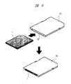
RS−MMC1をSDカードとして使用する場合には、SD型アダプタ(スロット、ケース)50を用いる。
【0051】
図8〜図10は、RS−MMCをSD型アダプタに装着する態様例を示す上面斜視図である。図8は、RS−MMCをSD型アダプタの短辺方向から挿入する例を示し、また、図9は、RS−MMCをSD型アダプタの表面から挿入する例を示し、また、図10は、RS−MMCをSD型アダプタの長辺方向から挿入する例を示す。
【0052】
このSD型アダプタは、図8〜図10に示すように、RS−MMC1が装着されるに足る空間(スペース)SPを有し、その外形は、SDカードとほぼ同じで、短辺約24mm、長辺約32mm、厚さ約2.1mmである。なお、図11に、SDカードの表面および裏面斜視図を示す。
【0053】
また、SD型アダプタ50の裏面斜視図である図12に示するように、SD型アダプタの裏面には、外部端子ACn(n:1〜9)が設けられている。この外部端子は、SD型アダプタの裏面側に露出した導電性部であり、SD型アダプタの内部に設けられた配線によって装着されるRS−MMCの外部端子Cnと電気的に接続される。
【0054】
図13に、SD型アダプタ50内にRS−MMC1を装着した際の要部平面図を示す。また、図14に、SD型アダプタの外部端子ACn(n:1〜9)、RS−MMCの外部端子Cn(n:1〜13)およびこれらの外部端子を接続するSD型アダプタの配線との関係を示す。
【0055】
図示するように、例えば、SD型アダプタの外部端子AC1は、RS−MMCの外部端子C1に接続され、同様にAC2は、C2に、AC3は、C3に、AC4は、C4に、AC5は、C5に、AC6は、C6に、AC7は、C7に、AC8は、C8に、AC9は、C9に、接続される。
【0056】
言い換えれば、SD型アダプタの内部には、RS−MMCを装着した際にRS−MMCの外部端子Cnが当接する部位(内部端子部)から外部端子ACnを接続する配線55が形成されている。この配線55は、できるだけ交差しないよう引き回すことが好ましいが、SD型アダプタ内の配線層を複数層とすることで、各配線が交差するようなレイアウトにも対応することができる。
【0057】
なお、図13に示すSt1は、スイッチでありこのスイッチ(スライド部品)の位置によりSD型アダプタの形状が変化する。この変化を例えばホスト側の電子装置で認識することにより、データの書き込みの可否を切り替えることができる。
【0058】
(2)本実施の形態のICカード(RS−MMC)をMSカードとして使用する場合について説明する。
【0059】
(2−1)RS−MMCをMSカードとして使用する場合には、MS型アダプタを用いる。
【0060】
図15は、RS−MMCをMS型アダプタに装着する態様例を示す表面斜視図であり、図16は、裏面斜視図である。図15および図16においては、RS−MMCをMS型アダプタの短辺方向から挿入する例を示す。また、図17は、RS−MMCをMS型アダプタに装着する態様例を示す裏面斜視図であり、RS−MMCをMS型アダプタの長辺方向から挿入する例を示す。また、図18は、RS−MMCをMS型アダプタに装着する態様例を示す表面斜視図であり、RS−MMCをMS型アダプタの表面から挿入する例を示す。
【0061】
このMS型アダプタ60は、図15〜図18に示すように、RS−MMC1が装着されるに足る空間(スペース)SPを有し、その外形は、MSカードとほぼ同じで、短辺約21.5mm、長辺約50mm、厚さ約2.8mmである。なお、図19に、MSカードの表面および裏面斜視図を示す。
【0062】
また、図16や図17に示すように、MS型アダプタ60の裏面には、外部端子ACn(n:1〜10)が設けられている。この外部端子は、MS型アダプタ60の裏面側に露出した導電性部であり、MS型アダプタ60の内部に設けられた配線によって装着されるRS−MMC1の外部端子Cnと電気的に接続される。
【0063】
図20に、MS型アダプタ60内にRS−MMC1を装着した際の要部平面図を示す。また、図21に、MS型アダプタ60の外部端子ACn(n:1〜10)、RS−MMCの外部端子Cn(n:1〜13)およびこれらの外部端子を接続するMS型アダプタの配線との関係を示す。
【0064】
図示するように、例えば、MS型アダプタの外部端子AC1は、RS−MMCの外部端子C3およびC6に接続され、同様にAC2は、C2に、AC3は、C4に、AC4は、C7に、AC5は、C8に、AC6は、C1に、AC7は、C9に、AC8は、C5に、AC9は、C4に、接続される。また、MS型アダプタの外部端子AC1は、AC10に接続され、また、AC3は、AC9に接続される。
【0065】
また、AC3とAC10との間には、抵抗R1およびR2が直列に接続され、これらの接続ノードNとAC10は、スイッチSt2を介して接続されている。また、ノードNは、外部端子C13と接続されている。また、スイッチSt2は、MS型アダプタの裏面に設けられた機械的なスイッチであり、例えばスイッチの位置を機械的に変化させることにより、接続ノードNとAC10とを導通状態とし(電気的に接続し)、もしくは非導通状態とする。
【0066】
このようにMS型アダプタの内部には、RS−MMC1を装着した際にRS−MMCの外部端子Cnが当接する部位(内部端子部)から外部端子ACnを接続する配線が形成されている。なお、(1)の欄で説明したように、MS型アダプタ内の配線層を複数層とすることで、各配線が交差するようなレイアウトにも対応することができる。
【0067】
このようなMS型アダプタ60によれば、MS型アダプタの外部端子ACnとRS−MMCの外部端子Cn間に抵抗(R1、R2)を設けたので、例えばRS−MMCの外部端子Cnが電源電位よりわずかに低い電位(プルアップ電位)もしくは接地電位よりわずかに高い電位(プルダウン電位)かを認識することができ、RS−MMCのモード切り替えを容易にすることができる。
【0068】
具体的には、図21に示すように、MS型アダプタの外部端子ACnには、種々の電位(信号)が印加される。図21の外部端子ACnの左側に印加される信号を示す。例えば、AC3には、電源電位(駆動電位、VCC)が、AC10には、接地電位(基準電位、VSS、GND)が印加される。なお、各信号については、項(5)において詳細に説明する。
【0069】
従って、C13の電位が接地電位より抵抗によって定まる所定の電位だけ高い(プルダウンされている)か否かで、MSカードとして機能するか否かを判定することができる。
【0070】
さらに、本実施の形態のMS型アダプタにおいては、抵抗R1とR2間の接続ノードNとAC10との間にスイッチSt2を配置したので、スイッチSt2がオンしている場合と、オフしている場合とでC13の電位のレベルを変更することができる。
【0071】
例えば、スイッチSt2がオンしている場合(書き込み禁止モード)には、C13が完全プルダウンする。また、スイッチSt2がオフしている場合(書き込み可能モード)には、C13が中間プルダウンする。
【0072】
このように、C13のプルダウンの程度で、書き込み可否のモードを切り替えることができる。
【0073】
(2−2)このMSカードには、その外形がより小さいタイプ(メモリースティックデュオ、以下「MSDuoカード」という)が存在する。
【0074】
RS−MMCをMSDuoカードとして使用する場合には、MSDuo型アダプタを用いる。
【0075】
図22は、RS−MMCをMSDuo型アダプタに装着する態様例を示す裏面および表面斜視図であり、RS−MMCをMSDuo型アダプタの短辺方向から挿入する例を示す。また、図23は、RS−MMCをMSDuo型アダプタに装着する態様例を示す表面斜視図であり、RS−MMCをMS型アダプタの長辺方向から挿入する例を示す。また、図24は、RS−MMCをMS型アダプタに装着する態様例を示す表面斜視図であり、RS−MMCをMS型アダプタの表面から挿入する例を示す。
【0076】
このMSDuo型アダプタ70は、図22〜図24に示すように、RS−MMC1が装着されるに足る空間(スペース)SPを有し、その外形は、MSDuoカードとほぼ同じで、短辺約20mm、長辺約31mm、厚さ約1.6mmである。なお、図25に、MSDuoカードの表面および裏面斜視図を示す。
【0077】
また、図22に示すように、MSDuo型アダプタの裏面には、外部端子ACn(n:1〜10)が設けられている。この外部端子は、MSDuo型アダプタ70の裏面側に露出した導電性部であり、MSDuo型アダプタの内部に設けられた配線によって、装着されるRS−MMCの外部端子と電気的に接続される。
【0078】
なお、MSDuo型アダプタの外部端子ACn(n:1〜10)、RS−MMCの外部端子Cn(n:1〜13)およびこれらの外部端子を接続するMSDuo型アダプタの配線等との関係は、図21を参照しながら説明したMS型アダプタの場合と同様であるため、その説明を省略する。
【0079】
従って、MS型アダプタの場合と同様に外部端子ACnとRS−MMCの外部端子Cn間に抵抗(R1、R2)を設けることにより、外部端子のプルダウンの有無でモードの切り替えを行い、また、プルダウンの程度で、書き込み可否のモードを切り替えることができる。
【0080】
(3)本実施の形態のICカード(RS−MMC)をUSB対応メモリとして使用する場合について説明する。
【0081】
RS−MMCをUSB対応メモリとして使用する場合には、USB型アダプタ(USB端子付きスロット)を用いる。
【0082】
図26は、RS−MMCをUSB型アダプタに装着する態様例を示す表面斜視図であり、RS−MMC1をUSB型アダプタ80の短辺方向から挿入、即ち、USB端子の差込方向に挿入する例を示す。また、図27は、RS−MMCをUSB型アダプタに装着する態様例を示す表面斜視図であり、RS−MMCをUSB型アダプタの長辺方向から挿入、即ち、USB端子の差込方向に直交する方向に挿入する例を示す。また、図28は、RS−MMCをUSB型アダプタに装着する態様例を示す表面斜視図であり、RS−MMCをUSB型アダプタの表面から挿入する例を示す。
【0083】
このUSB型アダプタは、図26〜図28に示すように、RS−MMCが装着されるに足る空間(スペース)SPを有し、ケース部80aとUSB端子部80bとからなる。
【0084】
このUSB端子部80bには、例えば図26に示すように外部端子ACn(n:1〜4)が設けられている。この外部端子は、USB端子部の内壁に設けられた導電性部であり、ケース部80aの内部に設けられた配線によって装着されるRS−MMCの外部端子と電気的に接続される。
【0085】
図29に、USB端子部の外部端子ACn(n:1〜4)、RS−MMCの外部端子Cn(n:1〜13)およびこれらの外部端子を接続するケース部内の配線との関係を示す。
【0086】
図示するように、例えば、USB端子部の外部端子AC1は、RS−MMCの外部端子C4に接続され、同様にAC2は、C12に、AC3は、C11に接続される。また、AC4は、C3およびC6に接続され、また、AC4は、C10と抵抗R3を介して接続される。
【0087】
このようにケース部の内部には、RS−MMCを装着した際にRS−MMCの外部端子Cnが当接する部位(内部端子部)から外部端子ACnを接続する配線が形成されている。なお、(1)の欄で説明したように、USB型アダプタ内の配線層を複数層とすることで、各配線が交差するようなレイアウトにも対応することができる。
【0088】
このようなUSB型アダプタ80によれば、USB端子部の外部端子ACnとRS−MMCの外部端子Cn間に抵抗(R3)を設けたので、例えばRS−MMCの外部端子Cnが電源電位よりわずかに低い電位(プルアップ電位)もしくは接地電位よりわずかに高い電位(プルダウン電位)かを認識することができ、RS−MMC1のモード切り替えを容易にすることができる。
【0089】
具体的には、図29に示すように、USB型アダプタの外部端子ACnには、種々の電位(信号)が印加される。図29の外部端子ACnの左側に印加される信号を示す。例えば、AC4には、接地電位(GND)が印加される。
【0090】
従って、C10の電位が接地電位より抵抗によって定まる所定の電位だけ高い(プルダウンされている)か否かで、USB対応メモリとして機能するか否かを判定することができる。
【0091】
(4)本実施の形態のICカード(RS−MMC)1をフルサイズのMMCカードとして使用する場合は、図6を参照しながら説明したエクステンダー9を用いる。なお、このエクステンダーを装着し、ホスト(電子装置)に挿入した場合には、RS−MMCの外部端子Cn(n:1〜13)がホスト側の端子と接触し、信号の伝達が可能になる。従って、図6に示すエクステンダー9には、配線や空間は形成されていない。
【0092】
なお、RS−MMCを直接ホスト(電子装置)に挿入した場合には、RS−MMCの外部端子Cn(n:1〜13)がホスト側の端子と接触し、信号の伝達が可能になることは言うまでもない。
【0093】
また、前記(1)から(4)で説明したアダプタ等は、例えば樹脂によって成形された筐体の内部に、銅箔張りガラスエポキシ基板の表面の銅箔をエッチングすることで、配線を成形した配線基板を有し、この配線基板には装着されるRS−MMCの外部端子に接触するための内部端子が接続され、また、配線基板の配線の一部は外部端子の形状を成し、筐体の外部端子窓より露呈される。内部端子としては、例えば、折り曲げ加工された金属製の板ばねなど、RS−MMCの外部端子Cn(n:1〜13)に押圧力を加えることのできる形状もしくは機構を有するものであることが好ましい。
【0094】
(5)次いで、本実施の形態のICカード(RS−MMC)を前記いずれかのアダプタに装着し、もしくはICカード単体をホストにセットした際の各モードの切り替えの判定フローについて説明する。
【0095】
図30は、図7のコントローラIC17によるモードの判定方法(判定手順)と、判定されたモードにしたがってコントローラーIC17の機能を切り替える手順を示すフローチャートである。
【0096】
以下、このフローチャート(図30)および図7等を参照しながら説明する。
【0097】
ICカード1をホストにセットした後、電源を投入すると、セットアップ動作が開始し、RS−MMCの外部端子C3およびC6に接地電位(VSS、GND)が供給され、また、外部端子C4に電源電位(VCC)が供給される。
【0098】
(ステップ1)次いで、外部端子C10にプルダウンが有るか否かをプルダウン検出部35で判定する。この外部端子C10にプルダウンがある場合、即ち、図29等を参照しながら説明したUSB型アダプタ80にRS−MMC1が装着されている場合には、モードコントローラ33によってUSBモードが選択される。
【0099】
その後、USBモードI/Fコントローラによって、図31に示すように、RS−MMCの外部端子C11に、+Data端子を、C12に−Data端子を割り当てる。+Data端子は、データ信号用の端子であり、−Data端子は、前記データ信号の反転信号用の端子である。なお、RS−MMCの外部端子C3およびC6は、GND端子であり、外部端子C4は、VBus端子である。VBus端子は、例えば5Vの駆動電圧用の端子である。
【0100】
(ステップ2)次いで、外部端子C10にプルダウンが無い場合には、外部端子C13に中間プルダウンが有るか否かをプルダウン検出部35で判定する。この外部端子C13にプルダウンがあり、その電位が中間電位(中間プルダウン)である場合、即ち、図21等を参照しながら説明したMS型アダプタ60もしくはMSDuo型アダプタにRS−MMC1が装着されている場合には、モードコントローラ33によってMSモードが選択される。さらに、中間プルダウンである場合には、スイッチSt1が非導通状態であり、書き込み可能モードとなる。
【0101】
その後、MSモードI/Fコントローラによって、図32に示すように、RS−MMCの外部端子C1に、INS端子を、C2に、BS端子を、C5に、SCLK端子を、C7にDIO端子を、C8およびC9にRSV端子を割り当てる。
【0102】
INS端子は、スティック挿抜検出用の端子であり、BS端子は、シリアルプロトコルバスステート信号用の端子である。また、SCLK端子は、シリアルプロトコルクロック信号用の端子であり、DIO端子は、シリアルプロトコルデータ信号用の端子である。RSV端子は、リザーブ用の端子である。なお、RS−MMCの外部端子C3およびC6は、VSS端子であり、外部端子C4は、VCC端子である。VSS端子とは、接地電圧用の端子で、また、VCC端子とは、例えば3.3Vの駆動電圧用の端子である。
【0103】
(ステップ3)次いで、外部端子C13に中間プルダウンが無い場合には、そのプルダウンが、完全プルダウンであるか否かをプルダウン検出部35で判定する。この外部端子C13にプルダウンがあり、その電位が前記中間電位よりさらに低い場合、即ち、MS型アダプタもしくはMSDuo型アダプタにRS−MMCが装着されている場合には、モードコントローラによってMSモードが選択される。さらに、完全プルダウンである場合には、スイッチSt1が導通状態であり、書き込み禁止モードとなる。
【0104】
その後、MSモードI/Fコントローラによって、図32を参照しながら説明したように、外部端子Cnに各信号端子を割り付ける。
【0105】
(ステップ4)次いで、外部端子C13に完全プルダウンが無い場合、即ち、図13および図14等を参照しながら説明したSD型アダプタ50もしくは図6を参照しながら説明したエクステンダー9が装着されている場合、もしくはRS−MMC1単体がセットされている場合には、モードコントローラ33によってMMC/SDモードが選択される。
【0106】
さらに、この後、以下に示す手順に従って「SPIモード」、「×4ビットモード(SDモード)」、「×8ビットモード(高速MMCモード)」もしくは「×1ビットモード(標準MMCモード)」の選択を行う。
【0107】
(ステップ4−1)まず、外部端子C2がリセットコマンドを受信中に、外部端子C1のチップセレクト(CS)信号がアサートされるか否かを判定する。
【0108】
CS信号がアサートされる場合には、SPIモード41dが、MMC/SDモードI/Fコントローラ41によって選択される。SPIモードでは、他のMMC(1ビット、8ビット)モードと異なりコマンド信号の伝送が単方向となる。
【0109】
外部端子Cnと信号端子との関係は図33に示す通りである。即ち、RS−MMCの外部端子C2は、DI端子、C5は、SCLK端子、C7は、DO端子である。このDI端子は、入力データ信号(DI)用の端子であり、DO端子は、出力データ信号(DO)用の端子である。また、C1は、CS信号用の端子であり、C3およびC6は、VSS端子であり、C4は、VCC端子である。
【0110】
(ステップ4−2)C2にSDモード(×4ビットモード)のCMD(起動コマンド)信号が入力された場合には、SDモード起動準備完了の応答をし、SDモード(×4ビットモード)41bが選択される。
【0111】
外部端子Cnと信号端子との関係は図34に示す通りである。即ち、RS−MMCの外部端子C1は、CD/DAT3端子、C5は、CLK端子、C7は、DAT0端子、C8およびC9は、DAT1端子およびDAT2端子である。CD/DAT3端子は、ホスト側にメモリカードを装着したことを伝えるカードディテクト(CD)信号もしくは第3データ信号(DAT3)用の端子である。DAT0端子、DAT1端子およびDAT2端子は、それぞれ第0データ信号(DAT0)用の端子、第1データ信号(DAT1)用の端子、第2データ信号(DAT2)用の端子である。また、C2は、CMD信号用の端子であり、C3およびC6は、VSS端子であり、C4は、VCC端子である。
【0112】
(ステップ4−3)C2に高速MMCモード(×8ビットモード)のCMD(起動コマンド)信号が入力された場合は高速MMCモード(×8ビットモード)41cが選択される。
【0113】
外部端子Cnと信号端子との関係は図35に示す通りである。即ち、RS−MMCの外部端子C1は、DAT3端子、C5は、CLK端子、C7は、DAT0端子、C8〜C13は、それぞれDAT1、DAT2およびDAT4〜DAT7端子である。DAT0端子は、第0データ信号(DAT0)用の端子であり、DAT1〜DAT7端子は、第1〜第7信号用(DAT1〜7)の端子である。また、C2は、CMD信号用の端子であり、C3およびC6は、VSS端子であり、C4は、VCC端子である。
【0114】
(ステップ4−4)CS信号のアサートも、SDモード(×4ビットモード)のCMD(起動コマンド)信号も、高速MMCモード(×8ビットモード)のCMD(起動コマンド)信号も入力されなかった場合には、標準MMCモード(×1ビットモード)41aが選択される。
【0115】
外部端子Cnと信号端子との関係は図36に示す通りである。即ち、RS−MMCの外部端子C1は、RSV/CS端子、C5は、CLK端子、C7は、DAT端子である。RSV/CS端子は、リザーブ信号(RSV)用の端子もしくはCS信号用の端子である。また、C2は、CMD信号用の端子であり、C3およびC6は、VSS端子であり、C4は、VCC端子である。
【0116】
このように本実施の形態のICカードによれば、プルダウン検出部35、モードコントローラ33、およびUSBモードI/Fコントローラ37やMSモードI/Fコントローラ39等、他規格のメモリのI/Fコントローラを設けたので、他規格のメモリとして使用することができる。
【0117】
また、このようなコントローラIC17を装着される基本ICカード内に組み込んだので、アダプタにコントローラを設ける必要がなく、アダプタのコスト低減を図ることができる。
【0118】
例えば、アダプタ側に他規格へのモード切り替え機能(35、33、37、39等)を設けることも可能であるが、この場合、アダプタ側にも半導体チップ(IC)を設ける必要があり、コスト高となる。
【0119】
しかしながら、本実施の形態のようにプルダウン検出部およびモードコントローラをICカード内に設けておけば、アダプタ側には、配線や抵抗等、容易に、また、安価に形成できる素子を設けるだけで他規格のメモリとの互換性を図ることができる。
【0120】
なお、本実施の形態においては、他規格のメモリとしてSDカード、MSカード、USB対応メモリを例に説明したが、この他の規格との互換性を図るI/Fコントローラを設けてもよい。また、互換性を図る他の規格の数は、3つに限られず、2以上であればよい。
【0121】
また、本実施の形態によれば、USB型アダプタやMS型アダプタにプルダウン用の抵抗を設けたが、抵抗を用いるアダプタ種は適宜変更可能である。
【0122】
また、本実施の形態においては、プルダウンを例に説明したが、プルアップでもよく、抵抗を介することによる電位の変化を適宜信号として利用することができる。また、検出部としてアダプタ側の外部端子であって、信号端子とならない端子間のショートの有無を判定する検出部を設けてもよい。
【0123】
(実施の形態2)
本実施の形態においては、実施の形態1で説明したRS−MMCカードのアダプタへの装着方向およびアダプタ側の内部端子形状について説明する。
【0124】
(1)図37は、RS−MMC1を、実施の形態1において例えば図8を参照しながら説明したように、アダプタADの短辺方向から挿入する場合の、アダプタ側の内部端子形状を示す斜視図である。
【0125】
図示するように、アダプタADにRS−MMC1を挿入した際、RS−MMCの外部端子Cnは、アダプタADの内壁に形成された内部端子BCnと接続される。この内部端子BCnは、バネ式の端子で、その平面パターンは、略矩形状であり、内部端子の長辺は、RS−MMCの挿入方向(アダプタおよびRS−MMCの長辺が延びる方向)に延在する。また、内部端子BCnは、RS−MMCの長辺が延びる方向に沿った断面が山形(凸型)となっている。
【0126】
このように、アダプタ側の内部端子BCnをカードの挿入方向に長い端子とし、または、アダプタ側の内部端子BCnを山形とすることで、RS−MMCの抜き差しの際にアダプタの内部端子およびRS−MMCの外部端子に加わる応力を低減することができ、RS−MMCの外部端子との接着を確実にすることができる。なお、図中の破線は、RS−MMCの外部端子の当接領域を示す(図40および図41において同じ)。
【0127】
実施の形態1において説明した図13(SD型アダプタ内にRS−MMCを装着した際の要部平面図)および図20(MS型アダプタ内にRS−MMCを装着した際の要部平面図)に、本実施の形態の内部端子BCnを配置した場合の要部平面図をそれぞれ図38および図39に示す。
【0128】
(2)図40は、RS−MMC1を、実施の形態1において例えば図10を参照しながら説明したように、アダプタADの長辺方向から挿入する場合の、アダプタ側の内部端子形状を示す斜視図である。
【0129】
図示するように、アダプタ側の内部端子BCnは、その平面パターンは、略矩形状であり、内部端子の長辺は、RS−MMCの挿入方向(アダプタおよびRS−MMCの短辺が延びる方向)に延在する。また、内部端子は、RS−MMCの短辺が延びる方向に沿った断面が山形となっている。
【0130】
この場合も、アダプタ側の内部端子BCnをカードの挿入方向に長い端子とし、または、アダプタ側の内部端子BCnを山形とすることで、RS−MMCの抜き差しの際にアダプタの内部端子およびRS−MMCの外部端子に加わる応力を低減することができ、RS−MMCの外部端子間の接着を確実にすることができる。また、この場合、内部端子BCn間の間隔を確保しやすい。
【0131】
(3)図41は、RS−MMCを、実施の形態1において例えば図9を参照しながら説明したように、RS−MMC1をアダプタADの表面から挿入する場合の、アダプタ側の内部端子形状およびその装着工程を示す斜視図である。
【0132】
図示するように、アダプタ側の内部端子BCnは、その平面パターンは、略矩形状であり、内部端子の長辺は、RS−MMCの短辺が延びる方向に延在する。また、内部端子は、RS−MMCの短辺が延びる方向に沿った断面が山形となっている。
【0133】
なお、この場合、アダプタ側には、引っかけ爪91およびロック爪93が設けられており、これらの爪によりRS−MMC1を確実に固定することができる。
【0134】
なお、(1)〜(3)で説明したアダプタ側の内部端子BCnは、RS−MMCの13の端子のすべてに対応させて配置してもよいが、モードによって使用しない端子には、対応する内部端子を配置しなくてもよい。
【0135】
また、本実施の形態のアダプタADの形状は、SD型アダプタ、MS型アダプタ、MSDuo型アダプタおよびUSB型アダプタのいずれでも良い。
【0136】
また、本実施の形態で説明した内部端子BCnは、例えば、端部を山形に加工した金属短冊片の平坦面をアダプタ内の配線基板にはんだなどを用いて接着固定し、かつ前記固定された側と反対側の端部を固定されていない自由端とすることで、RS−MMCの外部端子Cn(n:1〜13)に押圧力を加えることのできる形状もしくは機構を有するように形成するのが好ましい。
【0137】
(実施の形態3)
本実施の形態においては、実施の形態1で説明したRS−MMCカードの各種アダプタの販売セット(販売キッド)について説明する。
【0138】
(1)図42は、RS−MMC1および各種アダプタのセットを示す、斜視図である。
【0139】
図示するように、RS−MMC1と、SD型アダプタ50、MS型アダプタ60、MSDuo型アダプタ70およびUSB型アダプタ80をセットとして顧客に提供することができる。
【0140】
この際、セット内のRS−MMCを複数個(×N)としてもよい。また、図6を参照しながら説明したエクステンダー9をセット内に含めてもよい。
【0141】
このように、RS−MMCと各種アダプタをセットで顧客に提供することにより、SDカード、MSカードもしくはUSB対応メモリの需要にも応えることができ、また、多種の電子装置に対応することができる。また、多種の電子装置間のデータ移動(書き込み、読み出し)に容易に対応することができる。
【0142】
(2)また、図43に示すように、各種アダプタのみをセットとして提供してもよい。図43は、各種アダプタのセットを示す、斜視図である。
【0143】
SD型アダプタ50、MS型アダプタ60、MSDuo型アダプタ70およびUSB型アダプタ80をセットとして顧客に提供することができる。この際、図6を参照しながら説明したエクステンダー9をセット内に含めてもよい。
【0144】
このようなアダプタを使用することで、多種の電子装置に対応することができる。また、多種の電子装置間のデータ移動(書き込み、読み出し)に容易に対応することができる。また、RS−MMC1のユーザーの拡大を図ることができる。
【0145】
(実施の形態4)
実施の形態1においては、アダプタ側に、配線や抵抗のみを設けたが、図44に示すように、モード判定コマンド用半導体チップCHを設けてもよい。
【0146】
図44は、MS型アダプタ60の外部端子ACn(n:1〜10)、RS−MMC1の外部端子Cn(n:1〜13)およびこれらの外部端子を接続するMS型アダプタの配線等の関係を示す平面図である。
【0147】
なお、MS型アダプタ60の外部端子ACnおよびRS−MMC1の外部端子Cnは、実施の形態1の(2)において図21を参照しながら説明したので、ここではその説明を省略する。また、外部端子ACnと外部端子Cnの接続関係についても、図21と同じ箇所については、その説明を省略し、異なる箇所についてのみ説明する。
【0148】
図示するように、例えば、MS型アダプタの外部端子AC3とAC10との間には、半導体チップCHが接続され、また、半導体チップCHとAC10は、スイッチSt2を介して接続されている。また、半導体チップCHは、外部端子C13と接続されている。なお、このスイッチSt2は、MS型アダプタ60の裏面に設けられた機械的なスイッチであり、例えばスイッチの位置を機械的に変化させることにより、半導体チップCHとAC10とを導通状態とし(電気的に接続し)、もしくは非導通状態とする。
【0149】
例えば、図45に示すフローチャートに従って、MSモードの書き込み可能モードもしくは書き込み禁止モードを選択することができる。
【0150】
ステップ2およびステップ3以外は、実施の形態1において図30を参照しながら説明した手順に従って判断可能であるため、ここでは、ステップ2および3についてのみ説明する。
【0151】
(ステップ2)書き込み可否決定用スイッチSt2が非導通状態の場合には、半導体チップCH中で書き込み可能モード用コマンドを発生し、外部端子C13に伝送する。書き込み可能モード用コマンドが入力された場合には、図7のモードコントローラ33によってMSモード(39)が選択され、さらに、書き込み可能モードとなる。
【0152】
(ステップ3)書き込み可否決定用スイッチSt2が導通状態の場合には、半導体チップCH中で書き込み禁止モード用コマンドを発生し、外部端子C13に伝送する。書き込み禁止モード用コマンドが入力された場合には、図7のモードコントローラ33によってMSモードが選択され、さらに、書き込み禁止モードとなる。
【0153】
次いで、外部端子C13から応答がない場合には、図30中のステップ4に進む。
【0154】
このように、図7中のプルダウンの検出部35を設けず、アダプタ側の半導体チップCHから伝送されるコマンドの有無でモードの切り替えを行ってもよい。
【0155】
このような場合、実施の形態1で説明したアダプタと比較し、半導体チップCH分のコストアップが生じる。
【0156】
一方、このようなコマンド発生機構をホスト(電子機器)側に設け、モードの切り替えを行ってもよい。
【0157】
しかしながら、このようなホスト対応に比べ本実施の形態のICカードおよびアダプタの方が、適用ホストの制限がなく、汎用性を高めることができる。
【0158】
また、半導体チップCHに要求される機能はコマンド発生機構のみであるという風に、機能を低く抑えることで、半導体チップ自身のコストを抑えることが可能となる。
【0159】
具体的には、ICカードの書き込みや読み出しに用いる回路、例えば、各種モードのI/Fコントローラ、等を構成する、複雑、大規模な回路はRS−MMC側(RS−MMC内のコントローラ)に設けるられているので、アダプタの半導体チップCHはこれらを必要としない。
【0160】
また、単なるコマンド発生回路のみであれば、これらを構成する回路が単純で、これらを有する半導体チップCHを比較的安価に形成することが可能であるため、アダプタ側の半導体チップCH内に搭載してもアダプタを安価にできる。
【0161】
また、各種アダプタで共通する機能(どのアダプタにも必要な機能)であって、単純な回路は、アダプタ側の半導体チップCH内に搭載することが好ましい。各種アダプタで半導体チップCHを共通化できる場合には、半導体チップCHのコストの低減を図ることができる。
【0162】
また、本実施の形態によれば、MS型アダプタに半導体チップCHを設けたが、半導体チップCHを用いるアダプタ種は適宜変更可能である。
【0163】
以上、本発明者によってなされた発明を実施の形態に基づき具体的に説明したが、本発明は前記実施の形態に限定されるものではなく、その要旨を逸脱しない範囲で種々変更可能であることはいうまでもない。
【0164】
【発明の効果】
本願によって開示される発明のうち、代表的なものによって得られる効果を簡単に説明すれば、以下の通りである。
【0165】
第1規格のICカード中に、複数の外部端子のうちの所定の外部端子の電位レベルを検出する検出部と、前記検出部に接続されたモードコントローラを設け、前記検出部の信号に基づき前記第1規格に対応する第1モードインターフェースコントローラもしくは第2規格に対応する第2モードインターフェースコントローラを適宜選択したので、第2規格のICカードとの互換性を図ることができる。
【0166】
また、第2規格のICカードの外形を有するアダプタに、前記第1規格のICカードを挿入することにより第2規格のICカードとの互換性を図ることができる。この際、アダプタ側には、配線や抵抗等、容易に、また、安価に形成できる素子を設けるだけで他規格のICカード等との互換性を図ることができる。
【図面の簡単な説明】
【図1】本発明の実施の形態1であるICカードの表面図および第1の側面図である。
【図2】本発明の実施の形態1であるICカードの裏面図、第2〜第3の側面図および裏面図のA−A’部の断面図である。
【図3】本発明の実施の形態1であるICカードの表面斜視図である。
【図4】本発明の実施の形態1であるICカードの裏面斜視図である。
【図5】本発明の実施の形態1であるICカードの要部断面図である。
【図6】本発明の実施の形態1であるICカードとエクステンダーとの関係を示す表面斜視図である。
【図7】本発明の実施の形態1であるICカードの機能を示すブロック図である。
【図8】本発明の実施の形態1であるICカード(RS−MMC)をSD型アダプタに装着する態様例を示す上面斜視図である。
【図9】本発明の実施の形態1であるICカード(RS−MMC)をSD型アダプタに装着する態様例を示す上面斜視図である。
【図10】本発明の実施の形態1であるICカード(RS−MMC)をSD型アダプタに装着する態様例を示す上面斜視図である。
【図11】SDカードの表面および裏面斜視図である。
【図12】本発明の実施の形態1であるSD型アダプタの裏面斜視図である。
【図13】本発明の実施の形態1であるSD型アダプタ内にRS−MMCを装着した際の要部平面図である。
【図14】本発明の実施の形態1であるSD型アダプタの外部端子、RS−MMCの外部端子およびこれらの外部端子を接続するSD型アダプタの配線との関係を示す平面図である。
【図15】本発明の実施の形態1であるICカード(RS−MMC)をMS型アダプタに装着する態様例を示す表面斜視図である。
【図16】本発明の実施の形態1であるICカード(RS−MMC)をMS型アダプタに装着する態様例を示す裏面斜視図である。
【図17】本発明の実施の形態1であるICカード(RS−MMC)をMS型アダプタに装着する態様例を示す裏面斜視図である。
【図18】本発明の実施の形態1であるICカード(RS−MMC)をMS型アダプタに装着する態様例を示す表面斜視図である。
【図19】MSカードの表面および裏面斜視図である。
【図20】本発明の実施の形態1であるMS型アダプタ内にRS−MMCを装着した際の要部平面図である。
【図21】本発明の実施の形態1であるMS型アダプタの外部端子、RS−MMCの外部端子およびこれらの外部端子を接続するMS型アダプタの配線等の関係を示す平面図である。
【図22】本発明の実施の形態1であるICカード(RS−MMC)をMSDuo型アダプタに装着する態様例を示す表面および裏面斜視図である。
【図23】本発明の実施の形態1であるICカード(RS−MMC)をMSDuo型アダプタに装着する態様例を示す表面斜視図である。
【図24】本発明の実施の形態1であるICカード(RS−MMC)をMSDuo型アダプタに装着する態様例を示す表面斜視図である。
【図25】MSDuoカードの表面および裏面斜視図である。
【図26】本発明の実施の形態1であるICカード(RS−MMC)をUSB型アダプタに装着する態様例を示す表面斜視図である。
【図27】本発明の実施の形態1であるICカード(RS−MMC)をUSB型アダプタに装着する態様例を示す表面斜視図である。
【図28】本発明の実施の形態1であるICカード(RS−MMC)をUSB型アダプタに装着する態様例を示す表面斜視図である。
【図29】本発明の実施の形態1であるUSB型アダプタの外部端子、RS−MMCの外部端子およびこれらの外部端子を接続するケース部内の配線との関係を示す平面図である。
【図30】本発明の実施の形態1であるICカードのコントローラICのモード切り替えの判定方法(判定手順)を示すフローチャートである。
【図31】本発明の実施の形態1であるICカードにおいてUSBモードI/Fコントローラが選択された場合の外部端子Cnと信号との関係を示す平面図である。
【図32】本発明の実施の形態1であるICカードにおいてMSモードI/Fコントローラが選択された場合の外部端子Cnと信号との関係を示す平面図である。
【図33】本発明の実施の形態1であるICカードにおいてMMC/SDモードI/Fコントローラが選択され、SPIモードが選択された場合の外部端子Cnと信号との関係を示す平面図である。
【図34】本発明の実施の形態1であるICカードにおいてMMC/SDモードI/Fコントローラが選択され、4ビットモードが選択された場合の外部端子Cnと信号との関係を示す平面図である。
【図35】本発明の実施の形態1であるICカードにおいてMMC/SDモードI/Fコントローラが選択され、8ビットモードが選択された場合の外部端子Cnと信号との関係を示す平面図である。
【図36】本発明の実施の形態1であるICカードにおいてMMC/SDモードI/Fコントローラが選択され、1ビットモードが選択された場合の外部端子Cnと信号との関係を示す平面図である。
【図37】本発明の実施の形態2であるICカード(RS−MMC)の挿入方向を示す平面図およびアダプタ側の内部端子形状を示す斜視図である。
【図38】本発明の実施の形態2であるSD型アダプタ内にRS−MMCを装着した際の要部平面図である。
【図39】本発明の実施の形態2であるMS型アダプタ内にRS−MMCを装着した際の要部平面図である。
【図40】本発明の実施の形態2であるICカード(RS−MMC)の挿入方向を示す平面図およびアダプタ側の内部端子形状を示す斜視図である。
【図41】本発明の実施の形態2であるICカード(RS−MMC)の挿入方向を示す平面図およびアダプタ側の内部端子形状を示す斜視図である。
【図42】本発明の実施の形態3であるICカード(RS−MMC)および各種アダプタのセットを示す斜視図である。
【図43】本発明の実施の形態3である各種アダプタのセットを示す斜視図である。
【図44】本発明の実施の形態4であるMS型アダプタの外部端子、RS−MMCの外部端子およびこれらの外部端子を接続するMS型アダプタの配線等の関係を示す平面図である。
【図45】本発明の実施の形態4であるICカードのコントローラICのモード切り替えの判定方法(判定手順)を示すフローチャートである。
【図46】小型メモリカードの規格の一例として開発企業と商品名およびその外形寸法などを示す図表である。
【符号の説明】
1 ICカード(RS−MMC)
3 面取り部
5 エクステンダー装着部
7 溝部
9 エクステンダー
11 突起部
13 角部
14 金線
15 フラッシュメモリ(チップ)
16 ICカードチップ
17 コントローラIC(チップ)
19 ベース基板
21 封止樹脂
23 キャップ部
31 フラッシュメモリコントローラ
33 モードコントローラ
35 プルダウン検出部
37 USBモードI/Fコントローラ
39 MSモードI/Fコントローラ
41 MMC/SDモードI/Fコントローラ
41a ×1ビットモード
41b ×4ビットモード
41c ×8ビットモード
41d SPIモード
43 ICカードチップI/Fコントローラ
45 バスコントローラ
50 SD型アダプタ
55 配線
60 MS型アダプタ
70 MSDuo型アダプタ
80 USB型アダプタ
80a ケース部
80b USB端子部
91 引っかけ爪
93 ロック爪
ACn、AC1〜AC10 外部端子
AD アダプタ
BCn、BC1〜BC10 内部端子
Cn、C1〜C13 外部端子
CH 半導体チップ
N ノード
R1、R2 抵抗
R3 抵抗
St1 スイッチ
St2 スイッチ
SP 空間(スペース)[0001]
BACKGROUND OF THE INVENTION
The present invention relates to an IC card and an adapter, and more particularly to a technique effective when a specific IC card is used as another IC card having various shapes, pins (external terminals), and characteristics.
[0002]
[Prior art]
As a small-sized memory card, development of a memory card having a size of about a postage loaded with a nonvolatile memory (flash EEPROM: Electrically Erasable Programmable Read Only Memory) that can be electrically written and erased is underway.
[0003]
Many of such small memory cards have already been put into practical use as storage media for small devices such as digital cameras and mobile phones.
[0004]
However, there are a plurality of standards (external dimensions, number of pins, internal functions, etc.) of such a small memory card, and there are standards that are not compatible with each other. FIG. 46 shows a development company, a product name, its external dimensions, and the like as an example of a standard for a small memory card.
[0005]
For example, in the following Patent Document 1 (Japanese Patent Laid-Open No. 7-141114), the
[0006]
Further, in the following Patent Document 2 (Japanese Patent Laid-Open No. 2001-307801), the SD
[0007]
[Patent Document 1]
See JP-A-7-141114, summary and FIG.
[0008]
[Patent Document 2]
See Japanese Patent Application Laid-Open No. 2001-307801, abstract and FIG.
[0009]
[Problems to be solved by the invention]
As described above, it is an important consideration to achieve compatibility between various small memory cards using an adapter or the like.
[0010]
In addition, by reducing the size of the semiconductor chip built in the memory card, it meets the demand for smaller memory cards, increases the number of chips acquired from a single semiconductor wafer, and increases the product cost. Can be reduced.
[0011]
Therefore, the memory card of the same standard has been improved in performance including its outer shape.
[0012]
However, the new memory card is effective for use with the latest equipment compatible with this memory card, but cannot be used directly with the old model. In addition, the usage of memory cards has been diversified as functions of small devices have been improved.
[0013]
Therefore, it is important to improve compatibility with existing memory cards and take measures applicable to various devices in order to increase the demand for new memory cards and meet customer needs.
[0014]
An object of the present invention is to provide an IC card that can be compatible with other standard IC cards and the like by being attached to an adapter.
[0015]
Another object of the present invention is to provide an adapter used when the IC card is used as an IC card of another standard.
[0016]
The above and other objects and novel features of the present invention will be apparent from the description of this specification and the accompanying drawings.
[0017]
[Means for Solving the Problems]
Of the inventions disclosed in the present application, the outline of typical ones will be briefly described as follows.
[0018]
The IC card of the present invention is a first standard IC card, and (a) a plurality of external terminals, and (b) a detection unit that detects a potential level of a predetermined external terminal among the plurality of external terminals, (C) a mode controller connected to the detection unit; (d) a first mode interface controller connected to the mode controller and corresponding to the first standard; and a second mode interface controller corresponding to the second standard; (E) The mode controller includes means for selecting the first mode interface controller or the second mode interface controller based on a signal from the detection unit.
[0019]
The adapter of the present invention is an adapter having a space corresponding to the outer shape of the first standard IC card and having the outer shape of the second standard IC card, and (a) a plurality of first external terminals; (B) a plurality of internal terminals arranged at contact positions of a plurality of second external terminals of the first standard IC card when the first standard IC card is inserted into the space; A wiring connecting the first external terminal and the internal terminal; and (d) between the first external terminal to which a driving potential or a ground potential is applied and the internal terminal among the plurality of first external terminals. And a resistor connected to.
[0020]
DETAILED DESCRIPTION OF THE INVENTION
(Embodiment 1)
Hereinafter, embodiments of the present invention will be described in detail with reference to the drawings. Note that components having the same function are denoted by the same reference symbols throughout the drawings for describing the embodiments, and the repetitive description thereof is omitted.
[0021]
Hereinafter, the structure of an IC card (memory card) and an adapter according to an embodiment of the present invention will be described.
[0022]
1 to 5 are diagrams showing the structure of an IC card according to the present embodiment, FIG. 1 is a front view and a first side view of the IC card, and FIG. 2 is a back view of the IC card. FIG. 3 is a cross-sectional view taken along the line AA ′ of the second to third side views and the rear view. Each side view corresponds to a view seen from the direction of arrows (ad) in the plan view. FIG. 3 is a front perspective view of the
[0023]
As shown in the figure, the outer shape of the
[0024]
In addition, external terminals Cn (n: 1 to 13) are provided on the long side portion on the side where the chamfered
[0025]
The number of external terminals (number of pins) is not limited to 13. However, the number of external terminals needs to be equal to or greater than the maximum number of terminal functions in the IC card standard and the IC card standard for ensuring compatibility described later. .
[0026]
Further,
[0027]
As described above, the
[0028]
Such an
[0029]
In FIG. 5, for example, three chips (ICs) are incorporated. For example, the
[0030]
These
[0031]
The
[0032]
Note that the chip mounting form is not limited to that shown in FIG. 5. For example, the chip may be adhered to the lead frame and covered with a sealing resin, or mounted with only the base substrate and the cap. Can exist.
[0033]
Next, the internal functions of the IC card of this embodiment will be described. FIG. 7 is a block diagram showing functions of the IC card according to the present embodiment.
[0034]
Here, the IC card of the present embodiment is a first standard IC card, specifically, a multimedia card. The multimedia card (hereinafter referred to as “MMC card”) is a card based on a standard (hereinafter referred to as “MMC card standard”) defined by a multimedia card association (MMCA).
[0035]
The IC card of this embodiment is compatible with the following 2nd standard IC card (SD memory card), 3rd standard IC card (memory stick) and 4th standard IC card (USB compatible memory). Have. That is, the IC card (MMC) of this embodiment functions as an SD memory card, a memory stick, and a USB compatible memory.
[0036]
An SD (secure digital) memory card (hereinafter referred to as “SD card”) is a card based on a standard defined by the SD Card Association (hereinafter referred to as “SD card standard”), and is a card slightly thicker in the same shape as an MMC card. .
[0037]
Memory Stick (hereinafter referred to as “MS”) is a card developed by Sony Corporation. This card standard is called a Memory Stick card standard (MS card standard).
[0038]
USB is an abbreviation for “Universal Serial Bus” and is a specification for an interface for a personal computer for connecting peripheral devices. For example, the interface of a mouse, a keyboard, a printer, a modem, etc. is made common and only one USB connector is provided to facilitate the connection of the peripheral devices. Therefore, a memory (USB compatible memory) having a USB connector can be inserted into a USB terminal of a personal computer or the like and function as a memory.
[0039]
Many of the cards and the like are not compatible due to differences in standards, but compatibility can be ensured by using the IC card of the present embodiment as described below.
[0040]
As shown in the figure, an IC card (MMC card) 1 includes a
[0041]
The
[0042]
The
[0043]
The
[0044]
The
[0045]
The pull-
[0046]
Thus, according to the IC card of the present embodiment, the USB mode I /
[0047]
The IC card chip I /
[0048]
Mode switching by the
[0049]
(1) The case where the IC card (MMC card) of this embodiment is used as an SD card will be described. In the following description, the IC card of the present embodiment is indicated as “RS-MMC” in order to distinguish it from the full-
[0050]
When the RS-
[0051]
FIG. 8 to FIG. 10 are top perspective views showing examples of modes in which the RS-MMC is mounted on the SD type adapter. 8 shows an example in which RS-MMC is inserted from the short side direction of the SD type adapter, FIG. 9 shows an example in which RS-MMC is inserted from the surface of the SD type adapter, and FIG. The example which inserts RS-MMC from the long side direction of SD type | mold adapter is shown.
[0052]
As shown in FIGS. 8 to 10, this SD type adapter has a space SP enough to mount the RS-
[0053]
Further, as shown in FIG. 12, which is a rear perspective view of the
[0054]
In FIG. 13, the principal part top view at the time of mounting | wearing with the RS-MMC1 in SD type |
[0055]
As shown in the figure, for example, the external terminal AC1 of the SD type adapter is connected to the external terminal C1 of the RS-MMC. Similarly, AC2 is C2, AC3 is C3, AC4 is C4, and AC5 is AC5. AC5 is connected to C6, AC7 is connected to C7, AC8 is connected to C8, and AC9 is connected to C9.
[0056]
In other words, wiring 55 for connecting the external terminal ACn from a portion (internal terminal portion) where the external terminal Cn of the RS-MMC abuts when the RS-MMC is mounted is formed inside the SD adapter. The
[0057]
Note that St1 shown in FIG. 13 is a switch, and the shape of the SD adapter changes depending on the position of the switch (slide part). By recognizing this change by, for example, an electronic device on the host side, whether data can be written can be switched.
[0058]
(2) The case where the IC card (RS-MMC) of this embodiment is used as an MS card will be described.
[0059]
(2-1) When RS-MMC is used as an MS card, an MS type adapter is used.
[0060]
FIG. 15 is a front perspective view showing an example of mounting the RS-MMC on the MS adapter, and FIG. 16 is a rear perspective view. 15 and 16 show an example in which RS-MMC is inserted from the short side direction of the MS type adapter. FIG. 17 is a rear perspective view showing a mode example in which the RS-MMC is attached to the MS type adapter, and shows an example in which the RS-MMC is inserted from the long side direction of the MS type adapter. FIG. 18 is a front perspective view showing an example of mounting the RS-MMC on the MS type adapter, and shows an example of inserting the RS-MMC from the surface of the MS type adapter.
[0061]
As shown in FIGS. 15 to 18, this
[0062]
As shown in FIGS. 16 and 17, external terminals ACn (n: 1 to 10) are provided on the back surface of the
[0063]
In FIG. 20, the principal part top view at the time of mounting | wearing with RS-MMC1 in MS type |
[0064]
As shown in the figure, for example, the external terminal AC1 of the MS type adapter is connected to the external terminals C3 and C6 of the RS-MMC. Similarly, AC2 is C2, AC3 is C4, AC4 is C7, and AC5. Is connected to C8, AC6 is connected to C1, AC7 is connected to C9, AC8 is connected to C5, and AC9 is connected to C4. Further, the external terminal AC1 of the MS type adapter is connected to AC10, and AC3 is connected to AC9.
[0065]
Also, resistors R1 and R2 are connected in series between AC3 and AC10, and these connection nodes N and AC10 are connected via a switch St2. The node N is connected to the external terminal C13. The switch St2 is a mechanical switch provided on the back surface of the MS-type adapter. For example, by mechanically changing the position of the switch, the connection node N and the AC10 are made conductive (electrically connected). Or a non-conductive state.
[0066]
As described above, the wiring that connects the external terminal ACn from the portion (internal terminal portion) where the external terminal Cn of the RS-MMC abuts when the RS-
[0067]
According to such an
[0068]
Specifically, as shown in FIG. 21, various potentials (signals) are applied to the external terminal ACn of the MS adapter. 22 shows a signal applied to the left side of the external terminal ACn in FIG. For example, a power supply potential (drive potential, VCC) is applied to AC3, and a ground potential (reference potential, VSS, GND) is applied to AC10. Each signal will be described in detail in section (5).
[0069]
Therefore, whether or not to function as an MS card can be determined based on whether or not the potential of C13 is higher than the ground potential by a predetermined potential determined by the resistance (pulled down).
[0070]
Further, in the MS type adapter according to the present embodiment, the switch St2 is arranged between the connection node N between the resistors R1 and R2 and the AC10, so that the switch St2 is turned on and off. And the potential level of C13 can be changed.
[0071]
For example, when the switch St2 is on (write inhibit mode), C13 is completely pulled down. In addition, when the switch St2 is off (the writable mode), C13 pulls down intermediately.
[0072]
In this way, the write enable / disable mode can be switched with the degree of pull-down of C13.
[0073]
(2-2) This MS card has a smaller type (memory stick duo, hereinafter referred to as “MS Duo card”).
[0074]
When RS-MMC is used as an MSDuo card, an MSDuo type adapter is used.
[0075]
FIG. 22 is a rear surface and front perspective view showing an example in which the RS-MMC is mounted on the MSDuo adapter, and shows an example in which the RS-MMC is inserted from the short side direction of the MSDuo adapter. FIG. 23 is a front perspective view showing a mode example in which the RS-MMC is attached to the MSDuo type adapter, and shows an example in which the RS-MMC is inserted from the long side direction of the MS type adapter. FIG. 24 is a front perspective view showing an example of mounting the RS-MMC on the MS type adapter, and shows an example in which the RS-MMC is inserted from the surface of the MS type adapter.
[0076]
As shown in FIGS. 22 to 24, this MSDuo-
[0077]
Further, as shown in FIG. 22, external terminals ACn (n: 1 to 10) are provided on the back surface of the MSDuo adapter. This external terminal is a conductive part exposed on the back side of the
[0078]
The relationship between the external terminal ACn (n: 1 to 10) of the MSDuo type adapter, the external terminal Cn (n: 1 to 13) of the RS-MMC, and the wiring of the MSDuo type adapter connecting these external terminals is as follows: Since this is the same as the case of the MS type adapter described with reference to FIG. 21, the description thereof is omitted.
[0079]
Accordingly, as in the case of the MS type adapter, by providing resistors (R1, R2) between the external terminal ACn and the external terminal Cn of the RS-MMC, the mode is switched depending on whether or not the external terminal is pulled down. The write enable / disable mode can be switched to the extent of.
[0080]
(3) A case where the IC card (RS-MMC) of the present embodiment is used as a USB compatible memory will be described.
[0081]
When RS-MMC is used as a USB compatible memory, a USB adapter (slot with USB terminal) is used.
[0082]
FIG. 26 is a front perspective view showing a mode example in which the RS-MMC is attached to the USB adapter, and the RS-
[0083]
As shown in FIGS. 26 to 28, this USB adapter has a space SP enough to be fitted with an RS-MMC, and includes a
[0084]
The
[0085]
FIG. 29 shows the relationship between the external terminals ACn (n: 1 to 4) of the USB terminal unit, the external terminals Cn (n: 1 to 13) of the RS-MMC, and the wiring in the case unit that connects these external terminals. .
[0086]
As shown in the figure, for example, the external terminal AC1 of the USB terminal unit is connected to the external terminal C4 of the RS-MMC. Similarly, AC2 is connected to C12, and AC3 is connected to C11. AC4 is connected to C3 and C6, and AC4 is connected to C10 via a resistor R3.
[0087]
As described above, a wiring for connecting the external terminal ACn from a portion (internal terminal portion) where the external terminal Cn of the RS-MMC abuts when the RS-MMC is mounted is formed inside the case portion. As described in the section (1), by arranging a plurality of wiring layers in the USB adapter, it is possible to deal with a layout in which the respective wirings intersect.
[0088]
According to such a
[0089]
Specifically, as shown in FIG. 29, various potentials (signals) are applied to the external terminal ACn of the USB adapter. 30 shows a signal applied to the left side of the external terminal ACn of FIG. For example, a ground potential (GND) is applied to AC4.
[0090]
Therefore, whether or not to function as a USB-compatible memory can be determined based on whether or not the potential of C10 is higher than the ground potential by a predetermined potential determined by resistance (pulled down).
[0091]
(4) When the IC card (RS-MMC) 1 of the present embodiment is used as a full-size MMC card, the
[0092]
When the RS-MMC is directly inserted into the host (electronic device), the external terminal Cn (n: 1 to 13) of the RS-MMC is in contact with the terminal on the host side, and signal transmission is possible. Needless to say.
[0093]
In addition, the adapter described in the above (1) to (4), for example, formed wiring by etching the copper foil on the surface of the copper foil-clad glass epoxy substrate inside the housing formed of resin. An internal terminal for contacting the external terminal of the RS-MMC to be mounted is connected to the wiring board, and a part of the wiring of the wiring board forms the shape of the external terminal. It is exposed from the external terminal window of the body. The internal terminal may have a shape or mechanism that can apply a pressing force to the external terminal Cn (n: 1 to 13) of the RS-MMC, such as a bent metal leaf spring, for example. preferable.
[0094]
(5) Next, a determination flow for switching between modes when the IC card (RS-MMC) of the present embodiment is attached to any of the adapters or when the IC card alone is set in the host will be described.
[0095]
FIG. 30 is a flowchart showing a mode determination method (determination procedure) by the
[0096]
This will be described below with reference to this flowchart (FIG. 30) and FIG.
[0097]
When the power is turned on after setting the
[0098]
(Step 1) Next, the pull-
[0099]
Thereafter, as shown in FIG. 31, the USB mode I / F controller assigns a + Data terminal to the external terminal C11 of the RS-MMC and a -Data terminal to C12. The + Data terminal is a data signal terminal, and the -Data terminal is an inverted signal terminal of the data signal. The external terminals C3 and C6 of the RS-MMC are GND terminals, and the external terminal C4 is a VBus terminal. The VBus terminal is a terminal for driving voltage of 5V, for example.
[0100]
(Step 2) Next, when the external terminal C10 has no pull-down, the pull-
[0101]
After that, as shown in FIG. 32, the MS mode I / F controller has the RS-MMC external terminal C1, the INS terminal, the C2, BS terminal, the C5, the SCLK terminal, and the C7 DIO terminal. Assign RSV terminals to C8 and C9.
[0102]
The INS terminal is a terminal for stick insertion / extraction detection, and the BS terminal is a terminal for a serial protocol bus state signal. The SCLK terminal is a serial protocol clock signal terminal, and the DIO terminal is a serial protocol data signal terminal. The RSV terminal is a reserved terminal. The external terminals C3 and C6 of the RS-MMC are VSS terminals, and the external terminal C4 is a VCC terminal. The VSS terminal is a terminal for ground voltage, and the VCC terminal is a terminal for driving voltage of 3.3V, for example.
[0103]
(Step 3) Next, when there is no intermediate pull-down at the external terminal C13, the pull-
[0104]
Thereafter, as described with reference to FIG. 32, each signal terminal is assigned to the external terminal Cn by the MS mode I / F controller.
[0105]
(Step 4) Next, when there is no complete pull-down at the external terminal C13, that is, the
[0106]
Furthermore, after this, according to the procedure shown below, the “SPI mode”, “× 4 bit mode (SD mode)”, “× 8 bit mode (high-speed MMC mode)” or “× 1 bit mode (standard MMC mode)” Make a selection.
[0107]
(Step 4-1) First, it is determined whether or not the chip select (CS) signal of the external terminal C1 is asserted while the external terminal C2 is receiving the reset command.
[0108]
When the CS signal is asserted, the SPI mode 41d is selected by the MMC / SD mode I /
[0109]
The relationship between the external terminal Cn and the signal terminal is as shown in FIG. That is, the external terminal C2 of the RS-MMC is a DI terminal, C5 is an SCLK terminal, and C7 is a DO terminal. The DI terminal is a terminal for an input data signal (DI), and the DO terminal is a terminal for an output data signal (DO). C1 is a CS signal terminal, C3 and C6 are VSS terminals, and C4 is a VCC terminal.
[0110]
(Step 4-2) When the CMD (start command) signal of the SD mode (× 4 bit mode) is input to C2, the SD mode start preparation completion response is returned, and the SD mode (× 4 bit mode) 41b. Is selected.
[0111]
The relationship between the external terminal Cn and the signal terminal is as shown in FIG. That is, the external terminal C1 of the RS-MMC is a CD / DAT3 terminal, C5 is a CLK terminal, C7 is a DAT0 terminal, and C8 and C9 are a DAT1 terminal and a DAT2 terminal. The CD / DAT3 terminal is a terminal for a card detect (CD) signal or a third data signal (DAT3) that tells the host side that a memory card has been inserted. The DAT0 terminal, the DAT1 terminal, and the DAT2 terminal are a terminal for the 0th data signal (DAT0), a terminal for the first data signal (DAT1), and a terminal for the second data signal (DAT2), respectively. Further, C2 is a terminal for CMD signals, C3 and C6 are VSS terminals, and C4 is a VCC terminal.
[0112]
(Step 4-3) When a CMD (start command) signal in the high speed MMC mode (× 8 bit mode) is input to C2, the high speed MMC mode (× 8 bit mode) 41c is selected.
[0113]
The relationship between the external terminal Cn and the signal terminal is as shown in FIG. That is, the external terminal C1 of the RS-MMC is a DAT3 terminal, C5 is a CLK terminal, C7 is a DAT0 terminal, and C8 to C13 are DAT1, DAT2, and DAT4 to DAT7 terminals, respectively. The DAT0 terminal is a terminal for the 0th data signal (DAT0), and the DAT1 to DAT7 terminals are terminals for the 1st to 7th signals (DAT1 to 7). Further, C2 is a terminal for CMD signals, C3 and C6 are VSS terminals, and C4 is a VCC terminal.
[0114]
(Step 4-4) No CS signal was asserted, SD mode (× 4 bit mode) CMD (start command) signal, or high speed MMC mode (× 8 bit mode) CMD (start command) signal was not input In this case, the standard MMC mode (× 1 bit mode) 41a is selected.
[0115]
The relationship between the external terminal Cn and the signal terminal is as shown in FIG. That is, the external terminal C1 of the RS-MMC is an RSV / CS terminal, C5 is a CLK terminal, and C7 is a DAT terminal. The RSV / CS terminal is a reserve signal (RSV) terminal or a CS signal terminal. Further, C2 is a terminal for CMD signals, C3 and C6 are VSS terminals, and C4 is a VCC terminal.
[0116]
As described above, according to the IC card of the present embodiment, the pull-
[0117]
Further, since such a
[0118]
For example, it is possible to provide a mode switching function (35, 33, 37, 39, etc.) to another standard on the adapter side, but in this case, it is necessary to provide a semiconductor chip (IC) on the adapter side as well. Become high.
[0119]
However, if the pull-down detection unit and the mode controller are provided in the IC card as in this embodiment, it is only necessary to provide elements that can be easily and inexpensively formed on the adapter side, such as wiring and resistance. Compatibility with a standard memory can be achieved.
[0120]
In this embodiment, the SD card, the MS card, and the USB compatible memory have been described as examples of the other standard memory. However, an I / F controller for compatibility with the other standard may be provided. Further, the number of other standards for compatibility is not limited to three, and may be two or more.
[0121]
Further, according to the present embodiment, the pull-down resistor is provided in the USB adapter or the MS adapter, but the adapter type using the resistor can be changed as appropriate.
[0122]
In this embodiment, the pull-down is described as an example. However, pull-up may be used, and a change in potential due to a resistor can be used as a signal as appropriate. Further, a detection unit that is an external terminal on the adapter side and that determines whether there is a short circuit between terminals that do not become signal terminals may be provided as the detection unit.
[0123]
(Embodiment 2)
In the present embodiment, the mounting direction of the RS-MMC card described in the first embodiment to the adapter and the internal terminal shape on the adapter side will be described.
[0124]
(1) FIG. 37 is a perspective view showing the internal terminal shape on the adapter side when the RS-
[0125]
As illustrated, when the RS-
[0126]
In this way, the internal terminal BCn on the adapter side is a terminal that is long in the card insertion direction, or the internal terminal BCn on the adapter side is formed in a mountain shape, so that the internal terminal of the adapter and the RS- The stress applied to the external terminal of the MMC can be reduced, and adhesion with the external terminal of the RS-MMC can be ensured. In addition, the broken line in a figure shows the contact area | region of the external terminal of RS-MMC (same in FIG. 40 and FIG. 41).
[0127]
FIG. 13 (plan view of the main part when the RS-MMC is mounted in the SD type adapter) and FIG. 20 (plan view of the main part when the RS-MMC is mounted in the MS type adapter) described in the first embodiment FIG. 38 and FIG. 39 are main part plan views when the internal terminals BCn of the present embodiment are arranged.
[0128]
(2) FIG. 40 is a perspective view showing the internal terminal shape on the adapter side when the RS-
[0129]
As shown in the figure, the internal terminal BCn on the adapter side has a substantially rectangular plane pattern, and the long side of the internal terminal is in the RS-MMC insertion direction (the direction in which the short side of the adapter and the RS-MMC extends). Extend to. Moreover, the cross section along the direction where the short side of RS-MMC is extended has a mountain shape.
[0130]
Also in this case, the adapter-side internal terminal BCn is a terminal that is long in the card insertion direction, or the adapter-side internal terminal BCn is formed in a mountain shape, so that the adapter internal terminal and RS- Stress applied to the external terminals of the MMC can be reduced, and adhesion between the external terminals of the RS-MMC can be ensured. In this case, it is easy to ensure the interval between the internal terminals BCn.
[0131]
(3) FIG. 41 shows the internal terminal shape on the adapter side when the RS-
[0132]
As shown in the figure, the adapter internal terminal BCn has a substantially rectangular planar pattern, and the long side of the internal terminal extends in the direction in which the short side of the RS-MMC extends. Moreover, the cross section along the direction where the short side of RS-MMC is extended has a mountain shape.
[0133]
In this case, a hooking
[0134]
The adapter-side internal terminals BCn described in (1) to (3) may be arranged corresponding to all 13 terminals of the RS-MMC, but correspond to terminals that are not used depending on the mode. An internal terminal may not be arranged.
[0135]
The shape of the adapter AD of the present embodiment may be any of an SD type adapter, an MS type adapter, an MSDuo type adapter, and a USB type adapter.
[0136]
In addition, the internal terminal BCn described in the present embodiment is, for example, bonded and fixed to a wiring board in an adapter using a flat surface of a metal strip whose end is processed into a chevron using solder or the like. By forming the end opposite to the side as a free end that is not fixed, it is formed to have a shape or mechanism capable of applying a pressing force to the external terminal Cn (n: 1 to 13) of the RS-MMC. Is preferred.
[0137]
(Embodiment 3)
In the present embodiment, a sales set (sales kit) of various adapters of the RS-MMC card described in the first embodiment will be described.
[0138]
(1) FIG. 42 is a perspective view showing a set of the RS-
[0139]
As illustrated, the RS-
[0140]
At this time, a plurality of (× N) RS-MMCs in the set may be used. Further, the
[0141]
In this way, by providing the customer with RS-MMC and various adapters as a set, it is possible to meet the demand for SD cards, MS cards, or USB-compatible memories, and it is also possible to support various electronic devices. . Further, it is possible to easily cope with data movement (writing, reading) between various electronic devices.
[0142]
(2) Further, as shown in FIG. 43, only various adapters may be provided as a set. FIG. 43 is a perspective view showing a set of various adapters.
[0143]
The
[0144]
By using such an adapter, it is possible to deal with various electronic devices. Further, it is possible to easily cope with data movement (writing, reading) between various electronic devices. In addition, the number of users of the RS-
[0145]
(Embodiment 4)
In the first embodiment, only the wiring and the resistor are provided on the adapter side. However, as shown in FIG. 44, a mode determination command semiconductor chip CH may be provided.
[0146]
44 shows the relationship between the external terminals ACn (n: 1 to 10) of the
[0147]
Since the external terminal ACn of the
[0148]
As illustrated, for example, a semiconductor chip CH is connected between the external terminals AC3 and AC10 of the MS adapter, and the semiconductor chip CH and AC10 are connected via a switch St2. The semiconductor chip CH is connected to the external terminal C13. The switch St2 is a mechanical switch provided on the back surface of the MS-
[0149]
For example, according to the flowchart shown in FIG. 45, the MS mode writable mode or write inhibit mode can be selected.
[0150]
Since steps other than
[0151]
(Step 2) When the write enable / disable determining switch St2 is non-conductive, a write enable mode command is generated in the semiconductor chip CH and transmitted to the external terminal C13. When a writable mode command is input, the MS mode (39) is selected by the
[0152]
(Step 3) When the write enable / disable determining switch St2 is conductive, a write inhibit mode command is generated in the semiconductor chip CH and transmitted to the external terminal C13. When a write inhibit mode command is input, the MS mode is selected by the
[0153]
Next, when there is no response from the external terminal C13, the process proceeds to step 4 in FIG.
[0154]
As described above, the pull-
[0155]
In such a case, the cost for the semiconductor chip CH is increased as compared with the adapter described in the first embodiment.
[0156]
On the other hand, such a command generation mechanism may be provided on the host (electronic device) side to switch modes.
[0157]
However, the IC card and the adapter according to the present embodiment have no limitation on the applicable host and can improve versatility compared to such host correspondence.
[0158]
Further, it is possible to reduce the cost of the semiconductor chip itself by suppressing the function to a level that the function required for the semiconductor chip CH is only the command generation mechanism.
[0159]
Specifically, a complex and large-scale circuit constituting a circuit used for writing or reading an IC card, for example, an I / F controller in various modes, is provided on the RS-MMC side (controller in the RS-MMC). Since it is provided, the semiconductor chip CH of the adapter does not need these.
[0160]
Further, if only a command generation circuit is used, the circuits constituting these are simple, and the semiconductor chip CH having these can be formed at a relatively low cost. Therefore, the circuit is mounted in the semiconductor chip CH on the adapter side. But you can make the adapter cheaper.
[0161]
Moreover, it is preferable that a simple circuit that is a function common to various adapters (a function necessary for any adapter) is mounted in the semiconductor chip CH on the adapter side. When the semiconductor chip CH can be shared by various adapters, the cost of the semiconductor chip CH can be reduced.
[0162]
Further, according to the present embodiment, the semiconductor chip CH is provided in the MS type adapter, but the adapter type using the semiconductor chip CH can be changed as appropriate.
[0163]
As mentioned above, the invention made by the present inventor has been specifically described based on the embodiment. However, the present invention is not limited to the embodiment, and various modifications can be made without departing from the scope of the invention. Needless to say.
[0164]
【The invention's effect】
The effects obtained by the representative ones of the inventions disclosed by the present application will be briefly described as follows.
[0165]
In the IC card of the first standard, a detection unit for detecting a potential level of a predetermined external terminal among a plurality of external terminals, and a mode controller connected to the detection unit are provided, and based on the signal of the detection unit Since the first mode interface controller corresponding to the first standard or the second mode interface controller corresponding to the second standard is appropriately selected, compatibility with the IC card of the second standard can be achieved.
[0166]
Further, compatibility with the second standard IC card can be achieved by inserting the first standard IC card into an adapter having the outer shape of the second standard IC card. In this case, compatibility with other standard IC cards or the like can be achieved only by providing an element that can be easily and inexpensively formed on the adapter side, such as wiring and resistance.
[Brief description of the drawings]
1A and 1B are a front view and a first side view of an IC card according to a first embodiment of the present invention.
FIG. 2 is a back view of the IC card according to the first embodiment of the present invention, second to third side views, and a cross-sectional view taken along the line AA ′ of the back view.
FIG. 3 is a front perspective view of the IC card according to the first embodiment of the present invention.
FIG. 4 is a rear perspective view of the IC card according to the first embodiment of the present invention.
FIG. 5 is a cross-sectional view of a main part of the IC card according to the first embodiment of the present invention.
FIG. 6 is a front perspective view showing the relationship between the IC card and the extender according to the first embodiment of the present invention.
FIG. 7 is a block diagram showing functions of the IC card according to the first embodiment of the present invention.
FIG. 8 is a top perspective view showing a mode example in which the IC card (RS-MMC) according to the first embodiment of the present invention is attached to the SD type adapter.
FIG. 9 is a top perspective view showing a mode example in which the IC card (RS-MMC) according to the first embodiment of the present invention is attached to the SD type adapter.
FIG. 10 is a top perspective view showing an example in which the IC card (RS-MMC) according to the first embodiment of the present invention is attached to the SD adapter.
FIG. 11 is a front and back perspective view of an SD card.
FIG. 12 is a rear perspective view of the SD adapter according to the first embodiment of the present invention.
FIG. 13 is a plan view of a principal part when an RS-MMC is mounted in the SD type adapter according to the first embodiment of the present invention.
FIG. 14 is a plan view showing the relationship between the external terminal of the SD type adapter, the external terminal of the RS-MMC, and the wiring of the SD type adapter that connects these external terminals according to the first embodiment of the present invention;
FIG. 15 is a front perspective view showing an example in which the IC card (RS-MMC) according to the first embodiment of the present invention is attached to the MS type adapter.
FIG. 16 is a rear perspective view showing an example of an aspect in which the IC card (RS-MMC) according to the first embodiment of the present invention is attached to the MS type adapter.
FIG. 17 is a rear perspective view showing an example of an aspect in which the IC card (RS-MMC) according to the first embodiment of the present invention is attached to the MS type adapter.
FIG. 18 is a front perspective view showing a mode example in which the IC card (RS-MMC) according to the first embodiment of the present invention is attached to the MS type adapter.
FIG. 19 is a front and back perspective view of an MS card.
FIG. 20 is a plan view of relevant parts when an RS-MMC is mounted in the MS type adapter according to the first embodiment of the present invention.
FIG. 21 is a plan view showing the relationship between the external terminals of the MS type adapter according to the first embodiment of the present invention, the external terminals of the RS-MMC, the wiring of the MS type adapter connecting these external terminals, and the like.
FIG. 22 is a front and back perspective view showing an example of mounting the IC card (RS-MMC) according to the first embodiment of the present invention on an MSDuo type adapter;
FIG. 23 is a front perspective view showing a mode example in which the IC card (RS-MMC) according to the first embodiment of the present invention is attached to the MSDuo type adapter;
FIG. 24 is a front perspective view showing a mode example in which the IC card (RS-MMC) according to the first embodiment of the present invention is attached to the MSDuo adapter;
FIG. 25 is a front and back perspective view of the MSDuo card.
FIG. 26 is a front perspective view showing a mode example in which the IC card (RS-MMC) according to the first embodiment of the present invention is attached to the USB adapter.
FIG. 27 is a front perspective view showing an example in which the IC card (RS-MMC) according to the first embodiment of the present invention is attached to a USB adapter.
FIG. 28 is a front perspective view showing an example in which the IC card (RS-MMC) according to the first embodiment of the present invention is attached to a USB adapter.
FIG. 29 is a plan view showing the relationship between the external terminal of the USB adapter according to the first embodiment of the present invention, the external terminal of the RS-MMC, and the wiring in the case part connecting these external terminals.
FIG. 30 is a flowchart showing a mode switching determination method (determination procedure) of the controller IC of the IC card according to the first embodiment of the present invention.
FIG. 31 is a plan view showing a relationship between an external terminal Cn and a signal when a USB mode I / F controller is selected in the IC card according to the first embodiment of the present invention.
32 is a plan view showing the relationship between an external terminal Cn and a signal when the MS mode I / F controller is selected in the IC card according to the first embodiment of the present invention. FIG.
33 is a plan view showing a relationship between an external terminal Cn and a signal when the MMC / SD mode I / F controller is selected and the SPI mode is selected in the IC card according to the first embodiment of the present invention. FIG. .
34 is a plan view showing the relationship between an external terminal Cn and a signal when the MMC / SD mode I / F controller is selected and the 4-bit mode is selected in the IC card according to the first embodiment of the present invention. FIG. is there.
FIG. 35 is a plan view showing a relationship between an external terminal Cn and a signal when the MMC / SD mode I / F controller is selected and the 8-bit mode is selected in the IC card according to the first embodiment of the present invention. is there.
FIG. 36 is a plan view showing the relationship between the external terminal Cn and the signal when the MMC / SD mode I / F controller is selected and the 1-bit mode is selected in the IC card according to the first embodiment of the present invention. is there.
FIG. 37 is a plan view showing the insertion direction of the IC card (RS-MMC) according to the second embodiment of the present invention and a perspective view showing the internal terminal shape on the adapter side.
FIG. 38 is a plan view of relevant parts when an RS-MMC is mounted in the SD type adapter according to the second embodiment of the present invention.
FIG. 39 is a plan view of relevant parts when an RS-MMC is mounted in the MS type adapter according to the second embodiment of the present invention.
40 is a plan view showing an insertion direction of an IC card (RS-MMC) according to a second embodiment of the present invention and a perspective view showing an internal terminal shape on the adapter side. FIG.
41 is a plan view showing an insertion direction of an IC card (RS-MMC) according to a second embodiment of the present invention and a perspective view showing an internal terminal shape on the adapter side. FIG.
FIG. 42 is a perspective view showing a set of an IC card (RS-MMC) and various adapters according to the third embodiment of the present invention.
FIG. 43 is a perspective view showing a set of various adapters according to the third embodiment of the present invention.
FIG. 44 is a plan view showing the relationship between the external terminals of the MS type adapter according to the fourth embodiment of the present invention, the external terminals of the RS-MMC, and the wiring of the MS type adapter that connects these external terminals.
FIG. 45 is a flowchart showing a mode switching determination method (determination procedure) of the controller IC of the IC card according to the fourth embodiment of the present invention.
FIG. 46 is a chart showing a development company, a product name, its outer dimensions, and the like as an example of a standard of a small memory card.
[Explanation of symbols]
1 IC card (RS-MMC)
3 Chamfer
5 Extender mounting part
7 Groove
9 Extender
11 Protrusion
13 Corner
14 Gold wire
15 Flash memory (chip)
16 IC card chip
17 Controller IC (chip)
19 Base substrate
21 Sealing resin
23 Cap part
31 Flash memory controller
33 Mode controller
35 Pull-down detector
37 USB mode I / F controller
39 MS mode I / F controller
41 MMC / SD mode I / F controller
41a x 1 bit mode
41b x 4-bit mode
41c x 8-bit mode
41d SPI mode
43 IC card chip I / F controller
45 Bus controller
50 SD type adapter
55 Wiring
60 MS type adapter
70 MSDuo adapter
80 USB adapter
80a Case part
80b USB terminal
91 Claws
93 Locking claw
ACn, AC1 to AC10 External terminal
AD adapter
BCn, BC1 to BC10 Internal terminal
Cn, C1 to C13 External terminal
CH Semiconductor chip
N node
R1, R2 resistance
R3 resistance
St1 switch
St2 switch
SP space
Claims (6)
前記第1規格のICカードが挿入されることで、前記第1外部端子と接続される複数の第2外部端子を備えた第2規格のICカード外形を有するアダプタと、An adapter having a second standard IC card outer shape having a plurality of second external terminals connected to the first external terminals by inserting the first standard IC card;
を有するICカードであって、An IC card having
前記第1規格のICカードは、The IC card of the first standard is
電気的書き込みおよび消去が可能なフラッシュメモリチップと、A flash memory chip capable of electrical writing and erasing;
前記フラッシュメモリチップを制御するためのコントローラチップと、A controller chip for controlling the flash memory chip;
前記第1外部端子のうち、前記アダプタが外部装置と接続されることで電位レベルが変化する電位レベル検出端子と、Among the first external terminals, a potential level detection terminal whose potential level changes by connecting the adapter to an external device;
を有し、Have
前記コントローラチップは、そのチップ内に、The controller chip is in the chip,
前記第1規格のICカードに対応する第1モードインターフェースコントローラと、A first mode interface controller corresponding to the first standard IC card;
前記第2規格のICカードに対応する第2モードインターフェースコントローラと、A second mode interface controller corresponding to the second standard IC card;
前記電位レベル検出端子と接続され、電位レベルの変化を検出する検出部と、A detection unit connected to the potential level detection terminal to detect a change in potential level;
前記検出部の検出結果に応じて前記第1モードインターフェースコントローラから前記第2モードインターフェースコントローラに切り替えるモードコントローラと、A mode controller that switches from the first mode interface controller to the second mode interface controller according to the detection result of the detection unit;
前記フラッシュメモリチップの制御を行うためのフラッシュメモリコントローラと、A flash memory controller for controlling the flash memory chip;
前記第1モードインターフェースコントローラと前記フラッシュメモリコントローラとを接続する第1配線と、A first wiring connecting the first mode interface controller and the flash memory controller;
前記第2モードインターフェースコントローラと前記フラッシュメモリコントローラとを接続する前記第1配線とは別に設けられた第2配線と、A second wiring provided separately from the first wiring for connecting the second mode interface controller and the flash memory controller;
を備えていることを特徴とするICカード。An IC card characterized by comprising:
前記第1外部端子は、前記第2の辺よりも前記第1の辺に近くなるように配置され、The first external terminal is disposed closer to the first side than the second side,
前記フラッシュメモリチップは、前記第1の辺よりも前記第2の辺に近くなるように配置され、The flash memory chip is disposed closer to the second side than the first side,
前記コントローラチップは、前記第1外部端子と前記フラッシュメモリチップとの間に挟まれるように配置されていることを特徴とする請求項1記載のICカード。2. The IC card according to claim 1, wherein the controller chip is disposed so as to be sandwiched between the first external terminal and the flash memory chip.
前記フラッシュメモリコントローラは、前記第1外部端子よりも前記フラッシュメモリチップに近くなるように配置され、The flash memory controller is disposed closer to the flash memory chip than the first external terminal;
前記第1モードインターフェースコントローラ、および前記第2モードインターフェースコントローラは、前記第1外部端子と前記フラッシュメモリコントローラとの間に挟まれるように配置されていることを特徴とする請求項2記載のICカード。3. The IC card according to claim 2, wherein the first mode interface controller and the second mode interface controller are disposed so as to be sandwiched between the first external terminal and the flash memory controller. .
前記基板の裏面には、前記基板の表面の配線と電気的に接続された前記第1外部端子が配置され、The first external terminal electrically connected to the wiring on the front surface of the substrate is disposed on the back surface of the substrate,
前記基板の表面には、前記コントローラチップと前記フラッシュメモリチップとが配置され、The controller chip and the flash memory chip are arranged on the surface of the substrate,
前記基板の表面の配線、前記コントローラチップ、および前記フラッシュメモリチップは、金線により電気的に接続されていることを特徴とする請求項3または4記載のICカード。5. The IC card according to claim 3, wherein the wiring on the surface of the substrate, the controller chip, and the flash memory chip are electrically connected by a gold wire.
前記封止樹脂およびその周囲にある前記基板の表面を覆うようにキャップが設けられてA cap is provided to cover the surface of the sealing resin and the substrate around the sealing resin. いることを特徴とする請求項5記載のICカード。6. The IC card according to claim 5, wherein:
Priority Applications (11)
| Application Number | Priority Date | Filing Date | Title |
|---|---|---|---|
| JP2002296472A JP4236440B2 (en) | 2002-10-09 | 2002-10-09 | IC card |
| TW092126343A TW200410149A (en) | 2002-10-09 | 2003-09-24 | An IC card and an adapter for the same |
| US10/676,098 US20040070952A1 (en) | 2002-10-09 | 2003-10-02 | IC card and an adapter for the same |
| CNA2008100985987A CN101290663A (en) | 2002-10-09 | 2003-10-09 | Ic card and an adapter for the same |
| KR1020057006081A KR20060066666A (en) | 2002-10-09 | 2003-10-09 | I c card and adapter |
| PCT/JP2003/012974 WO2004034318A1 (en) | 2002-10-09 | 2003-10-09 | Ic card and adapter |
| AU2003271153A AU2003271153A1 (en) | 2002-10-09 | 2003-10-09 | Ic card and adapter |
| JP2004542861A JPWO2004034318A1 (en) | 2002-10-09 | 2003-10-09 | IC card and adapter |
| CNB2003801011605A CN100403334C (en) | 2002-10-09 | 2003-10-09 | IC card and an adapter |
| US11/681,046 US20070150633A1 (en) | 2002-10-09 | 2007-03-01 | Ic card and an adapter for the same |
| US12/261,993 US7823793B2 (en) | 2002-10-09 | 2008-10-30 | IC card and an adapter for the same |
Applications Claiming Priority (1)
| Application Number | Priority Date | Filing Date | Title |
|---|---|---|---|
| JP2002296472A JP4236440B2 (en) | 2002-10-09 | 2002-10-09 | IC card |
Related Child Applications (1)
| Application Number | Title | Priority Date | Filing Date |
|---|---|---|---|
| JP2008273005A Division JP4778547B2 (en) | 2008-10-23 | 2008-10-23 | IC card |
Publications (3)
| Publication Number | Publication Date |
|---|---|
| JP2005284323A JP2005284323A (en) | 2005-10-13 |
| JP2005284323A5 JP2005284323A5 (en) | 2006-11-09 |
| JP4236440B2 true JP4236440B2 (en) | 2009-03-11 |
Family
ID=32064142
Family Applications (2)
| Application Number | Title | Priority Date | Filing Date |
|---|---|---|---|
| JP2002296472A Expired - Fee Related JP4236440B2 (en) | 2002-10-09 | 2002-10-09 | IC card |
| JP2004542861A Pending JPWO2004034318A1 (en) | 2002-10-09 | 2003-10-09 | IC card and adapter |
Family Applications After (1)
| Application Number | Title | Priority Date | Filing Date |
|---|---|---|---|
| JP2004542861A Pending JPWO2004034318A1 (en) | 2002-10-09 | 2003-10-09 | IC card and adapter |
Country Status (7)
| Country | Link |
|---|---|
| US (3) | US20040070952A1 (en) |
| JP (2) | JP4236440B2 (en) |
| KR (1) | KR20060066666A (en) |
| CN (2) | CN101290663A (en) |
| AU (1) | AU2003271153A1 (en) |
| TW (1) | TW200410149A (en) |
| WO (1) | WO2004034318A1 (en) |
Cited By (1)
| Publication number | Priority date | Publication date | Assignee | Title |
|---|---|---|---|---|
| US10769091B2 (en) | 2018-01-03 | 2020-09-08 | Samsung Electronics Co., Ltd. | Memory card and electronic system |
Families Citing this family (111)
| Publication number | Priority date | Publication date | Assignee | Title |
|---|---|---|---|---|
| US20080185694A1 (en) * | 1999-08-04 | 2008-08-07 | Super Talent Electronics, Inc. | Processes of Manufacturing Portable Electronic Storage Devices Utilizing Lead Frame Connectors |
| JP2004227239A (en) * | 2003-01-22 | 2004-08-12 | Fujitsu Ltd | Conversion apparatus |
| TWI222009B (en) * | 2003-03-21 | 2004-10-11 | Carry Computer Eng Co Ltd | Universal micro memory card |
| TW595786U (en) * | 2003-06-11 | 2004-06-21 | C One Technology Corp | Micro electronic card with a plurality of different communication interfaces |
| KR100618814B1 (en) | 2003-07-04 | 2006-08-31 | 삼성전자주식회사 | Movable storage apparatus combined use of smart card capable of interfacing multi hosts and interfacing method of the same |
| TWI312468B (en) * | 2003-10-31 | 2009-07-21 | Ind Tech Res Inst | Method for data transmitting between an input-out card, and add-on memory card and a host system |
| FR2862409B1 (en) * | 2003-11-17 | 2006-04-14 | Datacard Inc | ADAPTER ELEMENT FOR PROGRAMMABLE ELECTRONIC SUPPORTS |
| US7159064B2 (en) * | 2003-12-11 | 2007-01-02 | Nokia Corporation | Method and device for increasing data transfer in multi-media card |
| JP4651332B2 (en) * | 2004-04-26 | 2011-03-16 | ルネサスエレクトロニクス株式会社 | Memory card |
| TWI271659B (en) * | 2004-05-05 | 2007-01-21 | Prolific Technology Inc | Memory card equipped with a multi-interface function and method for choosing a compatible transmission mode |
| US20050281010A1 (en) * | 2004-06-18 | 2005-12-22 | Super Talent Electronics, Inc. | Contact pad arrangement for integrated SD/MMC system |
| US7032827B2 (en) * | 2004-06-18 | 2006-04-25 | Super Talent Electronics, Inc. | Combination SD/MMC flash memory card with thirteen contact pads |
| JP4981271B2 (en) * | 2004-07-05 | 2012-07-18 | 三星電子株式会社 | Multi-mode integrated circuit device including mode detection and operation method thereof |
| TWI257583B (en) * | 2004-07-28 | 2006-07-01 | C One Technology Corp | Expandable reduced-size memory card and corresponding extended memory card |
| US7009846B1 (en) * | 2004-07-30 | 2006-03-07 | Super Talent Electronics, Inc. | 13-Pin socket for combination SD/MMC flash memory system |
| JP4591754B2 (en) * | 2004-07-30 | 2010-12-01 | ソニー株式会社 | COMMUNICATION DEVICE, ELECTRONIC DEVICE, AND COMMUNICATION SYSTEM |
| KR100579053B1 (en) * | 2004-08-26 | 2006-05-12 | 삼성전자주식회사 | Method of multi-interfacing between smart card and memory card and multi-interface card |
| US20060049265A1 (en) * | 2004-09-07 | 2006-03-09 | Richip Incorporated | Interface for a removable electronic device |
| CN100465933C (en) * | 2004-09-07 | 2009-03-04 | 瑞程科技股份有限公司 | Removable electronic device and its method |
| US7606947B2 (en) * | 2004-09-07 | 2009-10-20 | Industrial Technology Research Institute | Removable electronic device and method thereof |
| JP4480723B2 (en) * | 2004-09-24 | 2010-06-16 | 株式会社ルネサステクノロジ | Memory card and semiconductor device |
| US20060082986A1 (en) * | 2004-10-14 | 2006-04-20 | Chen Chi H | Housing for memory card |
| JP4543880B2 (en) * | 2004-10-27 | 2010-09-15 | ソニー株式会社 | Memory device |
| JP2006236261A (en) * | 2005-02-28 | 2006-09-07 | Renesas Technology Corp | Adapter for memory card, and memory card |
| JP2006268459A (en) * | 2005-03-24 | 2006-10-05 | Ricoh Co Ltd | Nonvolatile memory card and shape conversion adapter |
| KR100855262B1 (en) | 2005-03-24 | 2008-08-29 | 가부시키가이샤 리코 | Nonvolatile memory card adaptable to plural specifications |
| EP1727050B1 (en) * | 2005-05-27 | 2008-07-23 | STMicroelectronics S.r.l. | A method for embedded protocol selection, for instance in flash interfaces, related interface and computer program product |
| JP2007011708A (en) | 2005-06-30 | 2007-01-18 | Ricoh Co Ltd | Integrated-type memory card and shape transformation adaptor |
| KR100725981B1 (en) * | 2005-08-01 | 2007-06-08 | 삼성전자주식회사 | Multi-interface controller, memory card having the multi-interface controller, and method for setting interface |
| US20070032122A1 (en) * | 2005-08-03 | 2007-02-08 | 3 View Technology Co., Ltd | Electronic device with USB storage card |
| US7341194B2 (en) * | 2005-08-11 | 2008-03-11 | Chant Sincere Co., Ltd. | Adapter card |
| JP4449883B2 (en) * | 2005-10-20 | 2010-04-14 | ブラザー工業株式会社 | Storage medium connecting device and information device having the same |
| JP2007122354A (en) * | 2005-10-27 | 2007-05-17 | Nec Infrontia Corp | Peripheral device and electronic equipment system |
| US7739726B2 (en) * | 2005-11-14 | 2010-06-15 | Route1 Inc. | Portable device for accessing host computer via remote computer |
| US7320622B2 (en) * | 2005-11-14 | 2008-01-22 | Hon Hai Precision Ind. Co., Ltd. | Memory card adapter |
| US8070067B2 (en) * | 2005-12-22 | 2011-12-06 | Industrial Technology Research Institute | Receptacles for removable electrical interface devices |
| US20070145154A1 (en) * | 2005-12-22 | 2007-06-28 | Asustek Computer Incorporated | Interface for a removable electrical card |
| KR101223986B1 (en) * | 2006-02-23 | 2013-01-18 | 삼성전자주식회사 | Smart card and smart card system supporting plurality of interfaces |
| ES2288137A1 (en) * | 2006-03-09 | 2007-12-16 | Microelectronica Española S.A.U. | Smartcard and method for manufacturing said card |
| US20090111522A1 (en) * | 2006-03-09 | 2009-04-30 | Javier Canis Robles | Smart Card and Method for Manufacturing Said Card |
| JP2007280347A (en) * | 2006-03-14 | 2007-10-25 | Ricoh Co Ltd | Memory card and memory card control changeover method |
| CN100386776C (en) * | 2006-03-23 | 2008-05-07 | 骆建军 | Self-adaptive microSD storage card of multi-interface |
| CN100423024C (en) * | 2006-03-23 | 2008-10-01 | 骆建军 | Multiple interface self adaptive mini SD memory card |
| CN100423023C (en) * | 2006-03-23 | 2008-10-01 | 骆建军 | Multiple interface self adaptive rsMMC memory card |
| US20070260797A1 (en) * | 2006-05-03 | 2007-11-08 | Chien-yuan Chen | Memory card with an expansion function |
| WO2007138570A1 (en) * | 2006-05-26 | 2007-12-06 | Walletex Microelectronics Ltd. | Electrical adapter for coupling to a portable card and a portable card integral with such an adapter |
| JPWO2007141999A1 (en) * | 2006-06-02 | 2009-10-22 | 株式会社ルネサステクノロジ | Semiconductor device |
| TW200802124A (en) * | 2006-06-02 | 2008-01-01 | Stone Technology Internat Co Ltd | Memory card integrated with communication serial interface |
| TWM301452U (en) * | 2006-06-20 | 2006-11-21 | Chao-Chang Chen | Memory card and assembly thereof |
| KR100764744B1 (en) * | 2006-07-21 | 2007-10-08 | 삼성전자주식회사 | Device that identifies the interface protocol of host and ic-card including thereof |
| TW200820504A (en) * | 2006-10-31 | 2008-05-01 | Power Digital Card Co Ltd | Novel card structure |
| KR100770220B1 (en) * | 2006-10-16 | 2007-10-26 | 삼성전자주식회사 | Memory card and method of manufacturing the same |
| JP4956143B2 (en) * | 2006-11-02 | 2012-06-20 | 株式会社東芝 | Semiconductor memory card, host device, and data transfer method |
| US7367817B1 (en) * | 2006-11-09 | 2008-05-06 | Chin-Chun Liu | Housing of an electrical card |
| JP4646932B2 (en) * | 2007-02-27 | 2011-03-09 | 三洋電機株式会社 | Memory element |
| US8141782B2 (en) * | 2007-07-10 | 2012-03-27 | Inphase Technologies, Inc. | Dual-use media card connector for backwards compatible holographic media card |
| US8256677B2 (en) * | 2007-07-10 | 2012-09-04 | Inphase Technologies, Inc. | Enabling holographic media backwards compatibility with dual-use media card connector |
| JP2009059253A (en) * | 2007-08-31 | 2009-03-19 | Sony Corp | Card type peripheral device |
| JP4544281B2 (en) | 2007-08-31 | 2010-09-15 | ソニー株式会社 | Card type peripheral device |
| US8070057B2 (en) * | 2007-09-12 | 2011-12-06 | Devicefidelity, Inc. | Switching between internal and external antennas |
| US8915447B2 (en) * | 2007-09-12 | 2014-12-23 | Devicefidelity, Inc. | Amplifying radio frequency signals |
| US8109444B2 (en) * | 2007-09-12 | 2012-02-07 | Devicefidelity, Inc. | Selectively switching antennas of transaction cards |
| US9304555B2 (en) * | 2007-09-12 | 2016-04-05 | Devicefidelity, Inc. | Magnetically coupling radio frequency antennas |
| US9311766B2 (en) * | 2007-09-12 | 2016-04-12 | Devicefidelity, Inc. | Wireless communicating radio frequency signals |
| JP4438846B2 (en) | 2007-09-14 | 2010-03-24 | ソニー株式会社 | Card type peripheral device |
| KR100974663B1 (en) * | 2007-11-27 | 2010-08-09 | 주식회사 케이티 | Slot device connecting mobile phone for operating smart card and method thereof |
| WO2009118807A1 (en) * | 2008-03-24 | 2009-10-01 | 株式会社ルネサステクノロジ | Socket and semiconductor device |
| US8199725B2 (en) * | 2008-03-28 | 2012-06-12 | Research In Motion Limited | Rank indicator transmission during discontinuous reception |
| ITMI20080543A1 (en) * | 2008-03-31 | 2009-10-01 | Incard Sa | INTEGRATED CIRCUIT CARD INCLUDING REFINED ELECTRICAL CONTACTS. |
| KR101543582B1 (en) * | 2009-03-02 | 2015-08-11 | 삼성전자주식회사 | Memory card memory card reader and memory card system |
| JP5198379B2 (en) * | 2009-07-23 | 2013-05-15 | 株式会社東芝 | Semiconductor memory card |
| FR2949589B1 (en) * | 2009-09-03 | 2011-09-30 | Oberthur Technologies | ELECTRONIC DEVICE COMPRISING A MICROCIRCUIT CARD |
| US8301822B2 (en) * | 2009-09-23 | 2012-10-30 | Sandisk Il Ltd. | Multi-protocol storage device bridge |
| US8469271B2 (en) | 2009-10-22 | 2013-06-25 | Intellipaper, Llc | Electronic storage devices, programming methods, and device manufacturing methods |
| US8561910B2 (en) | 2009-10-22 | 2013-10-22 | Intellipaper, Llc | Memory programming methods and memory programming devices |
| US8469280B2 (en) | 2009-10-22 | 2013-06-25 | Intellipaper, Llc | Programming devices and programming methods |
| US8456850B2 (en) * | 2009-12-07 | 2013-06-04 | Samsung Electronics Co., Ltd. | Memory cards and electronic machines |
| CN104794523B (en) * | 2009-12-07 | 2018-10-12 | 三星电子株式会社 | Storage card and electronic device |
| JP5515919B2 (en) | 2010-02-12 | 2014-06-11 | ソニー株式会社 | Method for determining digital interface of electronic device and connected external device |
| WO2011127328A2 (en) | 2010-04-07 | 2011-10-13 | Intellipaper, Llc | Electronic assemblies and methods of forming electronic assemblies |
| USD643431S1 (en) * | 2010-05-17 | 2011-08-16 | Panasonic Corporation | Memory card |
| USD643432S1 (en) * | 2010-05-17 | 2011-08-16 | Panasonic Corporation | Memory card |
| USD639812S1 (en) * | 2010-05-17 | 2011-06-14 | Panasonic Corporation | Memory card |
| US8355670B2 (en) * | 2010-06-22 | 2013-01-15 | At&T Mobility Ii Llc | Near field communication adapters |
| KR101822977B1 (en) | 2010-12-21 | 2018-01-29 | 삼성전자주식회사 | Multi-interface memory card and operation method thereof |
| CA141195S (en) * | 2011-05-17 | 2012-02-03 | Sony Computer Entertainment Inc | Digital memory card |
| TW201249005A (en) * | 2011-05-27 | 2012-12-01 | Hon Hai Prec Ind Co Ltd | Storage card with a connector |
| CN102254202B (en) * | 2011-08-02 | 2013-06-19 | 四川和芯微电子股份有限公司 | Memory stick (MS) card control system and read-write method |
| USD667830S1 (en) * | 2011-11-29 | 2012-09-25 | Samsung Electronics Co., Ltd. | SD memory card |
| EP2600287A1 (en) * | 2011-12-01 | 2013-06-05 | Gemalto SA | Electronic device including elements managed by various standardised protocols and method for managing communication between said elements |
| USD669479S1 (en) * | 2012-01-13 | 2012-10-23 | Research In Motion Limited | Device smart card |
| USD669478S1 (en) * | 2012-01-13 | 2012-10-23 | Research In Motion Limited | Device smart card |
| US20130258576A1 (en) * | 2012-03-29 | 2013-10-03 | Gadi Ben-Gad | Memory Card |
| FR2989199B1 (en) * | 2012-04-04 | 2014-05-02 | Oberthur Technologies | ELECTRICALLY ACTIVE ADAPTER |
| AU2014247983B2 (en) * | 2013-04-05 | 2017-08-10 | Pny Technologies, Inc. | Reduced length memory card |
| US9413126B2 (en) * | 2013-04-23 | 2016-08-09 | Alan L. Pocrass | Combination USB connector and microSD flash card connector |
| USD736212S1 (en) * | 2014-07-01 | 2015-08-11 | Samsung Electronics Co., Ltd. | Memory card |
| USD736213S1 (en) * | 2014-07-01 | 2015-08-11 | Samsung Electronics Co., Ltd. | Memory card |
| USD736216S1 (en) * | 2014-07-30 | 2015-08-11 | Samsung Electronics Co., Ltd. | Memory card |
| USD739856S1 (en) * | 2014-07-30 | 2015-09-29 | Samsung Electronics Co., Ltd. | Memory card |
| USD783622S1 (en) * | 2015-08-25 | 2017-04-11 | Samsung Electronics Co., Ltd. | Memory card |
| USD783621S1 (en) * | 2015-08-25 | 2017-04-11 | Samsung Electronics Co., Ltd. | Memory card |
| USD772232S1 (en) * | 2015-11-12 | 2016-11-22 | Samsung Electronics Co., Ltd. | Memory card |
| USD773467S1 (en) * | 2015-11-12 | 2016-12-06 | Samsung Electronics Co., Ltd. | Memory card |
| USD814473S1 (en) * | 2016-01-19 | 2018-04-03 | Sony Corporation | Memory card |
| USD848431S1 (en) * | 2016-01-19 | 2019-05-14 | Sony Corporation | Memory card |
| JP6930854B2 (en) * | 2017-04-28 | 2021-09-01 | 新光電気工業株式会社 | Board module |
| CN109948767B (en) * | 2018-02-01 | 2024-08-09 | 华为技术有限公司 | Memory card and terminal |
| JP1621567S (en) * | 2018-06-13 | 2019-01-07 | ||
| US11763105B2 (en) | 2018-10-16 | 2023-09-19 | Huawei Technologies Co., Ltd. | Memory card, memory card adapter, and terminal device |
| US20220405225A1 (en) * | 2019-11-18 | 2022-12-22 | Hewlett-Packard Development Company, L.P. | Devices to select storage device protocols |
Family Cites Families (20)
| Publication number | Priority date | Publication date | Assignee | Title |
|---|---|---|---|---|
| JPH0390671U (en) | 1989-12-27 | 1991-09-17 | ||
| US5887145A (en) * | 1993-09-01 | 1999-03-23 | Sandisk Corporation | Removable mother/daughter peripheral card |
| JPH07141114A (en) | 1993-11-16 | 1995-06-02 | Canon Inc | Adaptor for memory card |
| US5752857A (en) * | 1996-05-24 | 1998-05-19 | Itt Corporation | Smart card computer adaptor |
| JP3104646B2 (en) * | 1997-06-04 | 2000-10-30 | ソニー株式会社 | External storage device |
| JPH11126450A (en) * | 1997-10-21 | 1999-05-11 | Fujitsu Ltd | Disk cartridge type adaptor capable of improving head construction and/or effectively using function of disk cartridge driving device |
| US6865096B1 (en) * | 1998-07-09 | 2005-03-08 | Illinois Tool Works Inc. | Power convertor with low loss switching |
| JP3250986B2 (en) * | 1999-01-21 | 2002-01-28 | 日本圧着端子製造株式会社 | Adapter for card connection |
| FI107973B (en) * | 1999-03-11 | 2001-10-31 | Nokia Mobile Phones Ltd | Method and means for using option cards in a mobile station |
| TW452152U (en) * | 1999-11-15 | 2001-08-21 | Kinpo Elect Inc | Seat commonly used for dual memory cards |
| JP4339477B2 (en) * | 2000-01-24 | 2009-10-07 | 日本圧着端子製造株式会社 | Adapter for card connection |
| JP3815936B2 (en) * | 2000-01-25 | 2006-08-30 | 株式会社ルネサステクノロジ | IC card |
| TWI244708B (en) * | 2000-03-30 | 2005-12-01 | Matsushita Electric Ind Co Ltd | Printed wiring board, IC card module using the same, and method for producing IC card module |
| JP2001307801A (en) | 2000-04-17 | 2001-11-02 | Kuurii Components Kk | Connector for memory card |
| JP3795725B2 (en) | 2000-04-21 | 2006-07-12 | 株式会社東芝 | Electronics |
| US6438638B1 (en) * | 2000-07-06 | 2002-08-20 | Onspec Electronic, Inc. | Flashtoaster for reading several types of flash-memory cards with or without a PC |
| DE60239383D1 (en) * | 2001-01-26 | 2011-04-21 | Sony Corp | IC CARD AND IC CARD ADAPTER |
| JP4416969B2 (en) * | 2001-07-30 | 2010-02-17 | キヤノン株式会社 | adapter |
| US6612492B1 (en) * | 2002-06-06 | 2003-09-02 | Chant Sincere Co., Ltd. | Four-in-one memory card insertion port |
| TW555110U (en) * | 2002-08-28 | 2003-09-21 | Carry Computer Eng Co Ltd | Adapter for xD memory card |
-
2002
- 2002-10-09 JP JP2002296472A patent/JP4236440B2/en not_active Expired - Fee Related
-
2003
- 2003-09-24 TW TW092126343A patent/TW200410149A/en unknown
- 2003-10-02 US US10/676,098 patent/US20040070952A1/en not_active Abandoned
- 2003-10-09 CN CNA2008100985987A patent/CN101290663A/en active Pending
- 2003-10-09 KR KR1020057006081A patent/KR20060066666A/en not_active Application Discontinuation
- 2003-10-09 WO PCT/JP2003/012974 patent/WO2004034318A1/en active Application Filing
- 2003-10-09 JP JP2004542861A patent/JPWO2004034318A1/en active Pending
- 2003-10-09 CN CNB2003801011605A patent/CN100403334C/en not_active Expired - Fee Related
- 2003-10-09 AU AU2003271153A patent/AU2003271153A1/en not_active Abandoned
-
2007
- 2007-03-01 US US11/681,046 patent/US20070150633A1/en not_active Abandoned
-
2008
- 2008-10-30 US US12/261,993 patent/US7823793B2/en not_active Expired - Fee Related
Cited By (2)
| Publication number | Priority date | Publication date | Assignee | Title |
|---|---|---|---|---|
| US10769091B2 (en) | 2018-01-03 | 2020-09-08 | Samsung Electronics Co., Ltd. | Memory card and electronic system |
| US11194752B2 (en) | 2018-01-03 | 2021-12-07 | Samsung Electronics Co., Ltd. | Memory card and electronic system |
Also Published As
| Publication number | Publication date |
|---|---|
| TW200410149A (en) | 2004-06-16 |
| US20070150633A1 (en) | 2007-06-28 |
| US20040070952A1 (en) | 2004-04-15 |
| WO2004034318A1 (en) | 2004-04-22 |
| AU2003271153A1 (en) | 2004-05-04 |
| US7823793B2 (en) | 2010-11-02 |
| AU2003271153A8 (en) | 2004-05-04 |
| JPWO2004034318A1 (en) | 2006-02-09 |
| CN100403334C (en) | 2008-07-16 |
| CN101290663A (en) | 2008-10-22 |
| KR20060066666A (en) | 2006-06-16 |
| JP2005284323A (en) | 2005-10-13 |
| US20090065593A1 (en) | 2009-03-12 |
| CN1703717A (en) | 2005-11-30 |
Similar Documents
| Publication | Publication Date | Title |
|---|---|---|
| JP4236440B2 (en) | IC card | |
| US7606947B2 (en) | Removable electronic device and method thereof | |
| US8070067B2 (en) | Receptacles for removable electrical interface devices | |
| US7291903B2 (en) | Memory card | |
| JP4864346B2 (en) | Memory card and card adapter | |
| KR101077123B1 (en) | Universal non-volatile memory card used with various different standard cards containing a memory controller | |
| US20060049265A1 (en) | Interface for a removable electronic device | |
| EP1801740B1 (en) | Interface for a removable electrical card | |
| KR100675011B1 (en) | Memory card pack | |
| JP4719687B2 (en) | Efficient connection between modules of removable electronic circuit cards | |
| US20050258243A1 (en) | Express card interface adapter for small storage media | |
| JP2007183776A (en) | Semiconductor device | |
| KR100843274B1 (en) | Memory card having double sided contact pad and method making that | |
| JP4778547B2 (en) | IC card | |
| JP4564321B2 (en) | Card type electronic equipment | |
| CN217404885U (en) | Memory card | |
| CN218333132U (en) | Storage device | |
| JP5019207B2 (en) | IC card and communication device | |
| JPH10278459A (en) | Ic card |
Legal Events
| Date | Code | Title | Description |
|---|---|---|---|
| A521 | Written amendment |
Free format text: JAPANESE INTERMEDIATE CODE: A523 Effective date: 20050830 |
|
| A621 | Written request for application examination |
Free format text: JAPANESE INTERMEDIATE CODE: A621 Effective date: 20050830 |
|
| AA91 | Notification of revocation by ex officio |
Free format text: JAPANESE INTERMEDIATE CODE: A971091 Effective date: 20060926 |
|
| A131 | Notification of reasons for refusal |
Free format text: JAPANESE INTERMEDIATE CODE: A131 Effective date: 20080826 |
|
| A521 | Written amendment |
Free format text: JAPANESE INTERMEDIATE CODE: A523 Effective date: 20081023 |
|
| TRDD | Decision of grant or rejection written | ||
| A01 | Written decision to grant a patent or to grant a registration (utility model) |
Free format text: JAPANESE INTERMEDIATE CODE: A01 Effective date: 20081125 |
|
| A01 | Written decision to grant a patent or to grant a registration (utility model) |
Free format text: JAPANESE INTERMEDIATE CODE: A01 |
|
| A61 | First payment of annual fees (during grant procedure) |
Free format text: JAPANESE INTERMEDIATE CODE: A61 Effective date: 20081216 |
|
| R150 | Certificate of patent or registration of utility model |
Free format text: JAPANESE INTERMEDIATE CODE: R150 |
|
| FPAY | Renewal fee payment (event date is renewal date of database) |
Free format text: PAYMENT UNTIL: 20111226 Year of fee payment: 3 |
|
| FPAY | Renewal fee payment (event date is renewal date of database) |
Free format text: PAYMENT UNTIL: 20111226 Year of fee payment: 3 |
|
| S111 | Request for change of ownership or part of ownership |
Free format text: JAPANESE INTERMEDIATE CODE: R313115 |
|
| FPAY | Renewal fee payment (event date is renewal date of database) |
Free format text: PAYMENT UNTIL: 20111226 Year of fee payment: 3 |
|
| R350 | Written notification of registration of transfer |
Free format text: JAPANESE INTERMEDIATE CODE: R350 |
|
| FPAY | Renewal fee payment (event date is renewal date of database) |
Free format text: PAYMENT UNTIL: 20111226 Year of fee payment: 3 |
|
| FPAY | Renewal fee payment (event date is renewal date of database) |
Free format text: PAYMENT UNTIL: 20121226 Year of fee payment: 4 |
|
| FPAY | Renewal fee payment (event date is renewal date of database) |
Free format text: PAYMENT UNTIL: 20121226 Year of fee payment: 4 |
|
| FPAY | Renewal fee payment (event date is renewal date of database) |
Free format text: PAYMENT UNTIL: 20131226 Year of fee payment: 5 |
|
| S531 | Written request for registration of change of domicile |
Free format text: JAPANESE INTERMEDIATE CODE: R313531 |
|
| R350 | Written notification of registration of transfer |
Free format text: JAPANESE INTERMEDIATE CODE: R350 |
|
| S111 | Request for change of ownership or part of ownership |
Free format text: JAPANESE INTERMEDIATE CODE: R313117 |
|
| S531 | Written request for registration of change of domicile |
Free format text: JAPANESE INTERMEDIATE CODE: R313531 |
|
| R350 | Written notification of registration of transfer |
Free format text: JAPANESE INTERMEDIATE CODE: R350 |
|
| LAPS | Cancellation because of no payment of annual fees |