JP4234397B2 - Chip module element and method for manufacturing the chip module element - Google Patents
Chip module element and method for manufacturing the chip module element Download PDFInfo
- Publication number
- JP4234397B2 JP4234397B2 JP2002329187A JP2002329187A JP4234397B2 JP 4234397 B2 JP4234397 B2 JP 4234397B2 JP 2002329187 A JP2002329187 A JP 2002329187A JP 2002329187 A JP2002329187 A JP 2002329187A JP 4234397 B2 JP4234397 B2 JP 4234397B2
- Authority
- JP
- Japan
- Prior art keywords
- capacitor
- capacitors
- array
- conductive
- layer
- Prior art date
- Legal status (The legal status is an assumption and is not a legal conclusion. Google has not performed a legal analysis and makes no representation as to the accuracy of the status listed.)
- Expired - Fee Related
Links
Images


Classifications
-
- G—PHYSICS
- G11—INFORMATION STORAGE
- G11C—STATIC STORES
- G11C29/00—Checking stores for correct operation ; Subsequent repair; Testing stores during standby or offline operation
- G11C29/04—Detection or location of defective memory elements, e.g. cell constructio details, timing of test signals
- G11C29/50—Marginal testing, e.g. race, voltage or current testing
-
- G—PHYSICS
- G11—INFORMATION STORAGE
- G11C—STATIC STORES
- G11C29/00—Checking stores for correct operation ; Subsequent repair; Testing stores during standby or offline operation
- G11C29/04—Detection or location of defective memory elements, e.g. cell constructio details, timing of test signals
- G11C2029/0403—Detection or location of defective memory elements, e.g. cell constructio details, timing of test signals during or with feedback to manufacture
-
- G—PHYSICS
- G11—INFORMATION STORAGE
- G11C—STATIC STORES
- G11C29/00—Checking stores for correct operation ; Subsequent repair; Testing stores during standby or offline operation
- G11C29/04—Detection or location of defective memory elements, e.g. cell constructio details, timing of test signals
- G11C29/50—Marginal testing, e.g. race, voltage or current testing
- G11C2029/5002—Characteristic
Landscapes
- Semiconductor Integrated Circuits (AREA)
- Production Of Multi-Layered Print Wiring Board (AREA)
Description
【0001】
【発明の属する技術分野】
本発明は、埋め込キャパシタに関する。さらに、詳記すると、本発明は、マルチチップモジュールにキャパシタを埋め込むための構造および方法を提供するものである。
【0002】
【従来の技術】
バイパスキャパシタは、半導体チップの近傍でマルチチップモジュール(MCM:Multi-Chip Module)に電荷の溜めを供給することによってパワーシステムを信号誘発変動から保護している。現在、高性能メインフレームコンピュータは、半導体チップの近傍でMCMに数百の表面実装型LICA(Low Inductance Capacitor Array:低インピーダンスキャパシタのアレイ)を利用している。このLICAは、MCMで価値のある表面エリアを消費し、現在のコストが1個当たり約3〜10米国ドルとなっている。
【0003】
MCMの周波数が増すにつれて、LICAの寄生直列インダクタンスが増大し、バイパスキャパシタとしてのLICAの有益性は減少する。直列インダクタンスが増大すると、所与の距離を越えて半導体チップに電荷を迅速に供給するキャパシタの能力は減退する。しかも、半導体チップの中心にあるスイッチングドライバからLICAキャパシタまでの距離は、これらのキャパシタが高周波における初期スイッチングノイズを減衰させるのをフライト時間が阻止するほど十分に離れている。周波数が〜1GHzに増加するのに従って、寄生インダクタンスのインピーダンスは、LICAのコンポーネントパフォーマンスを支配するポイントへと増大する。従って、LICAは、約1GHzの周波数を超えると、限られた有益性を有することになる。
【0004】
LICとチップとの間の距離およびインダクタンスが薄膜MCMの厚さおよびインダクタンスよりも大きいことを認めた上で、GHzレベルの周波数におけるバイパスキャパシタの問題を解決しようとするならば、薄膜キャパシタを薄膜MCM内部に埋め込むことが1つの解決策である。このような解決策であれば、MCM側のさらなるアクティブコンポーネントのために高周波(>1GHz)の性能を提供し、より多くの適用分野を開拓することができる。
【0005】
【発明が解決しようとする課題】
ビルドアッププロセス(buildup process)を使ってMCMを作るとき、埋め込まれた薄膜キャパシタの層に何らかの欠陥が生じる可能性がある。このような欠陥は、MCMを使用不能にする接地短絡への要因になりかねない。このような事態を回避するためには、全てのキャパシタをその接続に先立ち、後のビルドアップ層になる部分に至るまでテストすることが可能であろう。これは、ビルドアップ構造において、良好なキャパシタと欠陥のあるキャパシタとの考え得る全ての組み合わせに分割されたマスクが使用できないと、極めて困難である。キャパシタの数が多い場合、このようなマルチマスクを使用するアプローチの仕方は非常に現実的ではない。従って、必要なのは、上記した課題を克服する構造および方法であり、これが本発明の対象である。
【0006】
【課題を解決するための手段】
本発明の第1の形態によれば、キャパシタのアレイを形成し、該キャパシタのアレイ中の前記キャパシタを電気的にテストし、欠陥のあるキャパシタを示すデータと容認できるキャパシタを示すデータとを備えるテストデータを生成し、該テストデータを情報記憶媒体に保存し、前記キャパシタのアレイの上に、容認できるキャパシタに電気的に結合された複数の導電性エレメントを含む相互接続構造を形成し、該相互接続構造の形成は、前記キャパシタのアレイの上に接着性結合シートをラミネートし、前記容認できるキャパシタに隣接する前記結合シートに複数の開孔を形成すると共に、前記欠陥のあるキャパシタに隣接する前記結合シートには開孔を形成しないようにし、該開孔内部に導電性材料をデポジットすることを備える、ことを特徴とするチップモジュールエレメントを製造する方法が提供される。
また、本発明の第2の形態によれば、キャパシタのアレイと、該キャパシタのアレイに結合した平面状相互接続構造と、前記平面状相互接続構造に結合した多層回路構造であって、該平面状相互接続構造は前記キャパシタと該多層回路構造とを電気的に導通させる複数の導電性エレメントを備えているものと、前記多層回路構造に結合した複数の導電性ピンと、を備え、前記キャパシタのアレイは、前記ピンから前記多層回路構造を通り、導電性エレメントを通って前記キャパシタに至る電流を提供することによって充電され得るようになっており、接着性結合シートが、前記キャパシタのアレイの上にラミネートされ、前記欠陥のあるキャパシタに隣接する前記結合シートには開孔が形成されることなく、前記容認できるキャパシタに隣接する前記結合シートに複数の開孔が形成され、そして、導電性材料が、前記開孔内部にデポジットされている、ことを特徴とするチップモジュールエレメントが提供される。
本発明の実施例は、キャパシタのアレイを形成し、キャパシタのアレイを電気的にテストし、どのキャパシタが欠陥を有するか或いはどのキャパシタが容認できるか特定し、欠陥のあるキャパシタのデータを情報記憶媒体に保存することを備えるチップモジュールエレメント製造の方法を提供する。この方法は、さらに、キャパシタのアレイの表面に相互接続構造を形成することを備える。ここで、相互接続構造は、複数の導電性エレメント(例えば、導電性ポストおよびZ接続)を含み、導電性エレメントは容認できるキャパシタに電気的に結合されている。相互接続構造を形成することは、スパッタリング、無電解メッキ、電解メッキのうち少なくとも1つの方法を使用して複数の導電性エレメントを形成することを備える。或いは代わりに、相互接続構造の形成は、キャパシタのアレイの表面に接着結合シートをラミネート化させ、容認できるキャパシタに隣接する結合シートに複数の開孔を形成し、開孔内部に導電性材料をデポジットすることを備えてもよい。キャパシタのアレイの形成は、シリコン基板上にキャパシタのアレイを形成することを備えてもよい。
【0007】
本発明の実施例は、さらに、キャパシタのアレイ、このキャパシタのアレイに結合した平面状相互接続構造、および、この平面状相互接続構造の結合した多層回路構造を有するチップモジュールエレメントを提供する。相互接続構造は、キャパシタと多層回路構造を電気的に通じさせる複数の導電性エレメント(例えば、Z接続や導電性ポスト)を備える。多層回路構造には複数の導電性ピンが結合される。キャパシタのアレイは、前記ピンから多層回路構造を通過し、導電性エレメントを通過してキャパシタに至る電流を供給することによって充電され得る。
【0008】
【発明の実施の形態】
これらの提供物は、下記の説明が進むにつれて当業者に明らかになるであろう様々な副次的提供物および特徴と共に、本発明に係る方法およびチップモジュールエレメントによって獲得される。以下、その好ましい実施例を、単なる例としての添付図面を参照して詳細に説明される。
【0009】
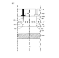
図1〜図8について詳細に説明すると、ここに示してあるのは、複数の誘電層を支持する基板12a(例えば、AlN(窒化アルミニウム)基板またはセラミック基板)を有する基板アセンブリ(全体的に10として描かれている)である。その全てが、以下に規定される。基板アセンブリ10は、キャパシタ16a、16b、16c、16d、16e、16f、16gからなるキャパシタのアレイ(全体的に16として描かれている)を含み、キャパシタのアレイ16の各キャパシタは、全てのキャパシタのための底部電極としての接地層18、電極層セグメント(以下、19a、19b等で表される)、および、これらの間の誘電層を含む。基板アセンブリ10は、また、多層回路構造54、相互接続構造58、並びに、電圧ピン60、61、接地ピン26a−26bおよび信号ピン63、64を含む。各キャパシタ(例えば、キャパシタ16a、16b等)は、何らかの適切な誘電体を含み、表面誘電層20全体にわたって平面状であっても非平面状であってもよい。一例に過ぎないが、図1〜図5に示す通り、キャパシタのアレイ16は、当業者によく知られている何らかの適切な手段によって形成することのできる共通の誘電層17を含む。
【0010】
接地層18は、好ましくは連続的で、接地ピン26a−26bに電気的に結合する。接地層18は、また、それぞれ接地パッド31a−31bと接地パッド33a−33bを含む導電性線路30、32を介して接地層24に電気的に結合する。キャパシタのアレイ16、すなわち、キャパシタ16a、16b、16c、16d、16e、16f、16gは、セグメント形電極層(全体的に19として描かれる)を含み、このセグメント形電極層の方は、一対のパッドとZ接続の複数の組み合わせからなる相互接続構造58を通して電極層36に結合する。詳述すると、下記のパッドとZ接続の組み合わせは、それぞれキャパシタ16a、16b、16c、16d、16e、16f、16gと関連する電極層セグメント19a、19b、19c、19d、19e、19fに結合する。その組み合わせとは、パッド37a、37bとZ接続38、パッド39a、39bとZ接続40、パッド41a、41bとZ接続42、パッド43a、43bとZ接続44、パッド45a、45bとZ接続46、パッド47a、47bとZ接続48、そして、パッド49a、49bとZ接続50である。ここでは、以下に述べるようなテストから、キャパシタ16d、16fに欠陥のあることが判明したと仮定する。そこで、導電性コラム(以下、89dおよび89fで表される)を点線で表し、これで、Z接続44、48が実際には形成されなかったが形成されたものとし、キャパシタ16d、16fが無欠陥または無傷で容認できることが判明したものとする。
【0011】
先に示した通ように、電極層19は、分割されたキャパシタ電極(すなわち、電極層セグメント19a、19b、19c、19d、19e、19f)にセグメント化されており、容認できるキャパシタのどれかと関連するピンのどれかに関して電圧または電荷がフローティングしている。セグメント形電極層19は、好ましくは、図1に示す通り、誘電層17の上に配置する。パッド(すなわち、パッド37b、39b、41b、43b、45b、47b、49b、図1参照)を、図9に最も良く示す通り、分割された電極層セグメント全ての上に直接載せてもよい。或いは代わりに、誘電層87をセグメント形電極層19および露出した誘電層17の上に配置し、次に、開口(図示されていない)を誘電層87に開け(例えば、レーザー78/コンピュータ80を使って)、続いて、図6、図7および図8に示す通り、電解メッキによって導電性コラム89、例えば、導電性コラム89cを形成してもよい。導電性コラム89dを点線で表し、これで、導電性コラム89dが実際には形成されなかったが、形成されたものとし、キャパシタ16dが無欠陥または無傷で容認できることが判明したことを示す。その後、パッド41b等を、導電性コラム89(例えば、図8に示す通りの導電性コラム89c)と接触するように誘電層87の上に配置する。
【0012】
キャパシタが容認できるかどうかテストするのに、パッド37b、39b、41b等を使用してもよい。詳記するならば、キャパシタ(すなわち、16a、16b、16c、16d、16e、16f、16g)のどれが短絡しているか特定するために、パッド(すなわち、パッド39b、41b、43b等)の各々を基板接地層(例えば、図1の接地層18)に関してテストしてもよい。そして、そのテストデータ(“合格”キャパシタ対“不合格”キャパシタのデータ)をコンピュータ80、詳記するならば、コンピュータ80のメモリバンク82に蓄積し、保存する(図2参照)。或いは代わりに、キャパシタの各々を、電極層セグメント19a、19b、19c、19d等を介して、パッドを介さずにテストしてもよい。
【0013】
集積回路チップのゲートがスイッチングに電荷を必要とすることは知られている。マルチチップモジュールでは、ゲートおよびチップの近傍に位置するキャパシタが、電荷の溜めとして働く。先に示した通り、キャパシタは、チップに近接する膜(例えば、誘電層17)を含む。これもまた先に示した通り、キャパシタのアレイ16を製造するプロセスでは、1つ以上のキャパシタに欠陥の生じることがあり得る。欠陥のあるキャパシタの短絡が、形成されたモジュールに欠陥を生じさせることもあり得る。
【0014】
本発明の実施例では、欠陥のあるキャパシタをチップから電気的に絶縁する。例えば、好ましい実施例では、キャパシタのアレイ16を、指示された手順に従って形成する。次に、このアレイ16を電気的にテストし、欠陥のあるキャパシタの場所のデータをコンピュータ80のメモリバンク82に保存する。次に、関連する電極層セグメント19a、19b、19c等を含むキャパシタのアレイ16全体の上に結合シート(例えば、誘電層87)を載置する。これにより、レーザー78または他のフライス削り手段が、保存された欠陥キャパシタの場所データを使って、合格キャパシタに見合う場所で結合シートに開孔(図示されていない)を開ける。これで、開孔を充填して導電性コラム、例えば、導電性コラム89cを生成できることになる。欠陥のあるキャパシタより上の領域は開放されない。つまり、キャパシタ16dが欠陥ありと仮定されたので、開孔89dは形成されなかったということになる。
【0015】
キャパシタのテストで欠陥ありとされたキャパシタの絶縁は、製造されたアセンブリにおいて行ってもよい。典型的に、キャパシタのテストは、先に示した通り、誘電層87およびパッド(例えば、パッド41b)を配置する前にも行われる。テスト手順の一例として、キャパシタにバイアス電圧をかけ、漏れ電流を測定することによって欠陥キャパシタをふるい分けることができる。そこで、漏れ電流の大きいキャパシタは、欠陥ありと判別されることになる。この情報は、次に、合格キャパシタにだけ電圧ビア(例えば、導電性コラム89c)が開けられるようにレーザーでドリリングするときに使用してもよい。合格キャパシタに開口を形成するのに使用されるレーザー78は、コンピュータ80によって操作される。欠陥キャパシタに関する情報は、レーザー78の動作を制御するコンピュータ80のメモリバンク82に保存される。レーザー78が欠陥キャパシタ(例えば、キャパシタ16d)の上方にあるとき、レーザー78がアクティブ化するのを阻止し、続いて、レーザーでドリリングを行うためにレーザー78を合格キャパシタの上方に移動させる。このようにして、コンピュータ80は、レーザードリリングのためにレーザー78を欠陥のない合格キャパシタの上方にだけ移動させていく。
【0016】
さらに、先に示した通り、開口95がレーザー78等の手段によって形成される。図1に示す本発明の実施例では、はんだを開口95の中にデポジットする。多層回路構造54(例えば、S層、V層またはG層とパッドを有する)を別個に形成し、結合シート(例えば、誘電層87)にラミネート化させることができる。欠陥キャパシタは、上方にZ接続を持たず、絶縁される。別個に形成された回路構造54を、そこで結合シートにラミネート化させる。合格キャパシタを荷電するための導電通路は、間接的である。電流が矢印A、BおよびCの方向に流れるにつれて、合格キャパシタが荷電される。図1に示す通り、電流は、Vピン60を通ってV平面または多層回路構造54の電極層36まで流れ、パッド37a、37bを通ってキャパシタ16aへと流れていくのである。
【0017】
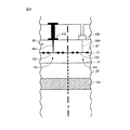
図4に示す本発明の実施例では、基板12b(例えば、シリコン基板)をZ接続アセンブリ13の中に通して基板12aに結合させる。ここで、Z接続アセンブリ13は、Z接続13a、13b、13c、13d、13e、13fを含む。基板12bは、相互接続構造58およびピン60、26a、63、41、26b、64によってキャパシタのアレイ16を支持する。従って、図3に示す本発明の実施例によれば、電気的通路が基板12bを通して形成され、結合シートの代わりに除去可能なマスク(例えば、SiN等のハードマスクまたはフォトレジスト)が使用される。図11に示す通り、適切なマスク材料の層97を層87の頂部または層17の頂部の上に配置する。そこで、レーザー78は開孔99を、開孔99が合格キャパシタ(例えば、キャパシタ16a、16b、16c、16d、16e、16g)と整合するように形成する。開孔99が形成された後、導電性ポストのアレイ70(すなわち、導電性ポスト70a、70b、70c、70d、70e)を合格キャパシタの上に、例えば、電解メッキによって形成する。直立する導電性ポストのアレイ70からマスクの層97を剥がす。これにより、標準のビルドアッププロセスを使って多層回路構造54(例えば、S層、V層またはG層とパッドを有する)を導電性ポストのアレイ70の上に形成することができる。
【0018】
図12〜図21について説明すると、そこに描かれているのは、高密度のスルーホールを有する多機能のマルチチップモジュール基板を作るための構造および方法である。将来のMCM基板は、入出力キャパシティを増大させるべく、より高い動作周波数、高いCPUカウント、そして、より細かいピンピッチを有するのが望ましい。ペロフスカイト型キャパシタ(perovskite capacitor)を埋め込んだマイクロ加工シリコン(micromachined Si)基板を使用することによって、これら3つの目標全てを達成することが可能となり得る。埋め込みペロフスカイト型キャパシタ材料、例えば、PZT、BST等は、イネーブル速度>GHzとモジュール面上のフリーアップエリアの両方に十分なバイパスキャパシタンスを提供できる。この材料を使用しなければ、フリーアップエリアは、今や追加CPUに使用できるLICA等、数百のばらばらなパッシブコンポーネントによって占領されることになる。マイクロ加工シリコンは、ペロフスカイト型キャパシタの高い歩留まりのための平面性と、スルービアのピッチを約1mmより小さい値に縮小する可能性の両方を提供する。基板において最高のスルーホール密度を達成するためには、シリコンのディープリアクティブイオンエッチング(DRIE:Deep Reactive Ion Etching)を使って、約100μm程度または約2mm前後の直径、450μm程度の低い値のピッチを有するSiのスルーホールビアにほぼ90度の壁を形成する。スルーホールは、この構造のユーティリティを確保すべく互いに電気的に絶縁しなければならない。両方のキャパシタを組入れ、スルービアを電気的に絶縁するためのプロセスおよび構造を図12〜図21に示す。詳述すると、図12〜図21は、高密度の導通スルーホールを有する多機能のマルチチップモジュール基板を作るための構造および方法を示す。強誘電性ペロフスカイトまたは寄生電気的ペロフスカイト(例えば、PZTまたはBST)の薄膜等、キャパシタンス密度の高い材料を使って最良の歩留まりを得るためには、シリコンウエハの平面状であることが高い歩留まりにとって極めて望ましい。
【0019】
より詳細に図12〜図21について説明すると、そこに見られるのは、厚さが約200μmから約3000μmまでの範囲のシリコン(Si)ウエハ100である。Siウエハ100は、二酸化ケイ素(SiO2)(すなわち、熱酸化物)を包む、厚さが約1μmから約3μmまでの範囲の層104に包まれている。SiO2包囲層104は、酸化環境の中でSiウエハ100から熱によって成長したものである。SiO2層104は、DRIEのためのエッチング止めとして機能させてもよい。SiO2包囲層104を定着させた後、Siウエハ100に構造的な支持を与え、ビア(下に、“116”で表される)が形成された後に平面性を確保するために、適切な誘電層108(例えば、Si3N4、酸窒化物、TEOS、LTO等)を図12の酸化構造の上にデポジットする。
【0020】
さらに、電極の接着状態または応力状態(例えば、引張応力または圧縮応力の度合い)を確保する目的で任意の誘電層110を誘電層108の上にデポジットさせてもよい。応力状態は、信頼性および歩留まり(例えば、クラッキング)およびキャパシタ歩留まり/性能に影響を及ぼし得る。ウエハ100の背側をプラズマ、レーザーまたは化学的方法によってドリリングし、それで、SiO2酸化物層104または誘電層108または110の上で止まるビア116を形成する(図15参照)。この工程は、場合によっては、当業者によく知られている予備ドリルマスキングプロセスとその後のマスク除去プロセスを必要とする。
【0021】
ビア116を互いに電気的に絶縁するために、その内部でSiO2熱酸化物層114を成長させる。SiO2酸化物層114は、厚さが例えば約0.25μmから約3.00μmまでの範囲内など、適切ないかなる厚さであってもよい。或いは代わりに、ビア116の表面のCVDパッシベーションなど、他の処理を施してもよい。本発明の別の実施例では、このとき、ビア116を導通媒体120で満たすことができる。
【0022】
キャパシタ118は、上側に任意の複数組のプロセスによって製造される。このとき、ビア116を導通媒体120で満たしてもよい(まだ行われていなかった場合)。接着を促進する層(例えば、TiN等)が最初に要求されることもあり得る。
【0023】
図18のウエハアセンブリの上側は、導通媒体120の上で止まるビア124を生成するために、プラズマ、レーザーまたは化学的方法によってドリリングする。このビア124は、直径がスルービア114より小さいものとする。このステップは、場合によっては、当業者によく知られている予備ドリルマスキングプロセスとその後のマスク除去プロセスを必要とする。ビア124に、金属または導通充填材からなるプレート128でライニングまたはメッキを施す。この工程は、場合によっては、(a)背側の導体シードのデポジションとその後のエッチングおよび/または(b)正面側のマスキングとその後のマスク除去を必要とする。
【0024】
本発明のある実施例では、130として連係的に大きく描かれたパッド、相互接続構造、経路等をマスクし、メッキする追加的プロセスを行ってもよい(まだ行われていない場合)。ピン止め、その後の層ビルドアップ、Z接続、表面マウント等の追加的プロセスをここで行ってもよい。
【0025】
図22〜図34について説明すると、そこに描かれているのは、並列処理膜を使って埋め込みコンポーネントを持つ多層電気基板を作るための構造および方法である。コンポーネントには、ICエレクトロニクスコンポーネントSi、GaAs、Si/Ge等、並びに、十分に小さい市販のパッシブコンポーネント(passive component)が含まれる。この構造は、高周波モジュール用途におけるバイパス使用のために多量のマイクロファラドのキャパシタンスを有する。価値あるコンポーネントを基板に埋め込むことは、周波数と密度の要求が市場を駆り立てるにつれて、ますます重要になってこよう。最新技術水準の要求を満たすためには、分離したコンポーネントをコスト効率の高い仕方で埋め込むことが必要になるケースもあり得る。
【0026】
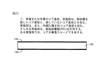
図22に見られるのは、単層または多層のコア基板130である。本発明の実施例は、銅被覆132を施したコア基板130と、施していないコア基板130とを含む。本発明の実施例はまた、内側Cu層を持つコア基板130も含む。本発明のさらなる実施例は、樹脂被覆銅(RRC)を利用する。先在する導通スルービアを使用する実施例も、本発明の主旨および範囲から逸脱することなく実現できる。
【0027】
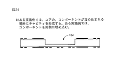
コア基板130がCu被覆132−132で形成された後、Cu被覆132−132は、図23の構造を生成するためにパターン化し、エッチングしてもよい。本発明の実施例は、減法的パターン化、加法的パターン化および半加法的パターン化の全てを含む。本発明のある実施例では、Cu被覆132を完全にエッチングし、コンポーネント(下に“140”で表される)を埋め込むべき場所を空ける。他の実施例では、コア基板130の両側にコンポーネントを埋め込む。図24に最も良く示す通りの追加的実施例では、予備形成される(例えば、フライス、カッタまたはドリルを使って)キャビティ134を、その後にコンポーネントが埋め込まれる場所に形成してもよい。内側Cu層を持つコア基板130の場合は、Cu層をレーザー止めとして使ってコアキャビティ134をレーザーで開けてもよい。
【0028】
131として大きく描かれた埋め込むべきコンポーネント140(図25参照)は、すでに作られた、好ましくは並列に作られた、同じく131として大きく描かれた分離した誘電膜(可能であれば、多層)または可撓膜の上に組み立てられる。ある実施例では、高温はんだ(例えば、Au−20Sn、Au−12Ge、Au−3.5SiまたはPb−5Sn)または導電性接着剤を使って、その後の処理およびコア基板130の使用における信頼性を確保する。他の実施例では、場合によっては、誘電膜131の上側となる下側にパッド層が存在しない。本発明の追加的実施例では、コア基板130の下側となるべく露出誘電膜131の表面にピン、スタッド瘤またははんだ瘤を取り付けてもよい。
【0029】
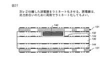
コア基板130(キャビティ134を一切持たない、すなわち、キャビティなしのコア基板130)にコンポーネント140(1つ以上の誘電膜を含む)を取り付ける様々な実施例を描いた図26〜図30について説明すると、図23のパターン化銅被覆コア基板130の上に誘電層144−144を置くか、流すか、展延させるか、吹付けるか、または、ラミネート化させる。或いは、プリカットされた“プリプレグ”(または、類似材料)のアライメントが必要となることもあり得る。誘電層144の1つに、コンポーネント140を受容するための誘電性キャビティ148を形成する。注目すべきは、補助の下込め材、“グロップトップ”、または、他の接着/密封材を任意に、後続の処理に先立ってコンポーネント140全体に施してもよいことである。誘電膜131は、取り付けられたコンポーネント140を含めて、図27に最も良く示す通り、コンポーネント140がキャビティ148の中に留まるように図26の層状構造にラミネート化してもよい。誘電膜131−131は、応力釣合いのために両側でラミネート化してもよい。
【0030】
引き続き、スルービア・アセンブリ150をドリル、デスミア、eレス、Cuシード/プレート、eプレートCuによって形成し、次に、スルービアを充填してから、パネル化する。誘電膜131の露出側にパッド層が存在しない実施例では、パターン化および/またはパッド層作成を行ってもよい。他の実施例では、スルービア・アセンブリ150にCuキャップをかぶせてもよい。追加的実施例では、二通りのドリリング工程を使用してよく、コア基板130を貫通しない程度のブラインドビア・アセンブリ154(図28参照)を形成してもよい。
【0031】
図29で見られるのは、ラミネート化の間に、技術的に知られたはんだ付けまたは導電性ペースト充填によって接着性誘電膜131に作られるZ接続158である。図30では、金属ポスト160(例えば、Cu)をコア基板130(または、コア基板130の上に留まるスペーサ)の上に立てる。この場合は、Z接続が、ラミネート化の間に、技術的に知られた薄肉はんだ、拡散結合過渡液または導電性ペースト充填によって接着性誘電膜に作られる。
【0032】
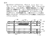
次に、キャビティのあるコア基板の様々な実施例を描いた図31〜図35について説明すると、パターン化銅被覆コア基板130の上に誘電層144−144を置くか、流すか、展延させるか、吹付けるか、または、ラミネート化させる。或いは、プリカットされた“プリプレグ”(または、類似材料)のアライメントが必要となることもあり得る。補助の下込め材、“グロップトップ”、または、他の接着/密封材料を任意に、後続の処理に先立ってコンポーネント140全体に施してもよい。引き続き、図32に最も良く示す通り、誘電膜131−131は、取り付けられたコンポーネント140を含めて、コンポーネント140がキャビティ148の中に留まるように図31の構造にラミネート化してもよい。
【0033】
誘電膜131−131は、図32に最も良く示す通り、応力釣合いのために両側でラミネート化してもよい。引き続き、スルービア・アセンブリ150をドリル、デスミア(desmear)、eレス(e-less)、Cuシード/プレート(Cu seed/plate)、eプレートCu(e-plate Cu)によって形成し、次に、スルービアを充填してから、パネル化する。誘電膜131の露出側にパッド層が存在しない実施例では、パターン化および/またはパッド層作成を行ってもよい。他の実施例では、ビアにCuキャップをかぶせてもよい。追加的実施例では、二通りのドリリング工程を使用してよく、コア基板130を貫通しない程度のブラインドビア・アセンブリ154を形成してもよい。
【0034】
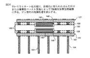
図34について説明すると、そこに見られるのは、ラミネート化の間に、技術的に知られたはんだ付けまたは導電性ペースト充填によって接着性誘電膜131に形成されたZ接続158である。ピン164を使用する両側処理(Double sided processing)を図34に示す。金属ポスト(例えば、Cu)160をコア基板130(または、コア上に留まるスペーサ)の上に立てる。この場合は、Z接続158を、ラミネート化の間に、技術的に知られた薄肉はんだ(thin solder)、拡散結合過渡液(diffusion bonding transient liquid)または導電性ペースト充填(conductive paste methodology)によって接着性誘電膜131に形成する。今や、埋め込みラミネートボードが、技術的によく知られている手段によって最終組み立てか誘電ビルドアップかどちらかのために使用可能(例えば、最終的なIC取り付けの組み立てのために使用可)である。或いは代わりに、積層ビアビルドアップ構造(stacked via build-up structure)またはもっと標準的な千鳥状ビア構造(staggered via structure)のためのポストメッキが、今や技術的に知られている通りに進行してもよい。
【0035】
先に示した通り、埋め込みペロフスカイト型キャパシタ材料、例えば、PZT、BST等は、イネーブル速度>GHzとモジュール面上のフリーアップエリア(free up real estate)の両方に十分なバイパスキャパシタンスを提供できる。この材料を使用しなければ、フリーアップエリアは、LICA等、数百のばらばらなパッシブコンポーネントによって占領されることになる。また、この材料は、周囲に沿って施されるLICAと対照的にチップの直ぐ近くに配置することができる。注意すべきは、ペロフスカイトがその処理温度(例えば、温度>600℃)の高さのために、ある種の基板材料(すなわち、有機ラミネート)の上で直接加工できないことである。
【0036】
図36〜図41について説明すると、そこに見られるのは、シリコン基板170に形成されたインピーダンス調整可能なスルービア構造168であり、また、スルービア構造168を製造する方法の図解である。
【0037】
シリコン基板を集積回路(IC)パッケージに組入れるために、これまで数通りのアプローチが開発されてきた。一例として、シリコンは、埋め込みパッシブコンポーネントを包含し、ICとPCBの間のCTE整合を可能にし、極めて高い経路密度を許容する等々の多機能インタポーザ(multifunctional interposer)として使用できる。基板170等のシリコン基板をインタポーザとして使用するには、シリコン基板170に、ICとPCBの間の接続を形成する垂直スルービア(例えば、図39のビア175)を提供しなければならない。シリコン基板170において、スルービアを適宜活用できるようにするためには幾つかの要件を満たさなければならない。信号反射等を最小限に抑えるために、ビアを導電性シリコン基板170から絶縁しなければならず、配線のインピーダンスを他のIC線およびPCB線のインピーダンスに整合しなければならない。ここで図39について説明すると、シリコン基板170は、多孔質シリコン領域179で包囲されたスルービア175を含んでおり、このスルービアは、ビア175をシリコン基板170から絶縁し、また、要件を満たすべくビア特性インピーダンスを調整するのに使用することができる。
【0038】
集積パッシブ、高密度相互接続、ディジタル機能から隔離されたRF機能、および、パッケージ内の光学系のためにマイクロ加工シリコンを使用するケースは、広く世界的に増えつつある。図39〜図40に描かれるように、新規のアプローチでは、50〜70Ωの範囲でコントロールされた一定の信号線路インピーダンスをマイクロ加工シリコンパッケージ内部に供給することができる。このようなパッケージ内部の信号インピーダンス整合は、将来の高周波パッケージの用途において不可避のものとなるであろう。シリコン基板170に形成されたビア175の構造を図36〜図39に示す。シリコン基板170は、マスク層176とフォトレジスト178で被覆する。フォトレジスト178をパターン化し、マスク層176においてスルーホール174を形成すべくエッチングする。これで、スルーホール174は、マスク層176を通してシリコン基板170に形成される。電気化学的な陽極処理技術を使って、多孔質シリコン領域179をスルーホール174の周囲に迅速に形成する。多孔質シリコン領域179の安定化を行う。マスク層176とフォトレジスト178を除去した後、スルーホール174をキャッピング層180で覆い、続いて、ビア175を金属メッキ184によって形成する。
【0039】
多孔質シリコン(PS:porous silicon)は、その幾つかの材料特性により、マイクロエレクトロニクスパッケージに使用するのが実際上有利とされる。シリコン構造の結晶性が高い上、材料密度が相対的に高い(レギュラーシリコンの20〜80%)にも拘わらず、多孔質シリコンは絶縁材となっている。抵抗率が10mΩ・cmと低い高導電性シリコン基板に形成されたとしても、多孔質シリコンは、最大限1012Ω・cmの抵抗率を持つことができる。その多孔質の性質のために、多孔質シリコンは誘電率が2と極めて低い。しかしながら、標準的な有孔率(30〜60%)の材料であっても、誘電率はε=3〜6の範囲内である。
【0040】
フッ化水素酸の濃縮水溶液または濃縮エタノール溶液の中で、シリコン基板170を陽極エッチングすることによって多孔質シリコンを形成する。基板のドーピング条件またはエッチング条件に応じて、異なる種類の多孔質シリコンを作ることができる。エッチング速度は10μm/min程度高くてよく、従って、相対的に短い時間でシリコンに大きい多孔質領域を形成することができる。
【0041】
多孔質シリコンがスルーホール174を包む絶縁構造を形成するのに数通りのプロセスフローを使用してもよい。一例に過ぎないが、シリコン基板170を、金属でも誘電体でもよい薄いマスク層176で覆う。唯一の要件は、マスク176がフッ化水素酸濃縮液に溶けてはならないことである。基板170は、次に、フォトリソグラフィによってパターン化されたフォトレジスト178で被覆する。マスク層176は、フォトレジスト178を通してパターン化される。スルーホール174を、例えば、DREI(deep reactive ion etching)を使ってシリコンにエッチングする。フッ化水素酸溶液中での陽極処理により、多孔質シリコン領域179がスルーホール174の周囲に迅速に形成される。ウエハの残りはフォトレジスト178で覆われるので、多孔質シリコンはスルーホール174の内側にしか形成されない。多孔質シリコンの表面を、250〜300℃の酸素雰囲気中での熱焼鈍によって安定させる(予備酸化)。形成された多孔質シリコン179を覆うため、この上にキャッピング層180、例えば、CVD酸化シリコン層をデポジットする。これにより、予備酸化された多孔質シリコンは、大気汚染および水の吸い上げから保護される。
【0042】
ここで注目すべきは、多孔質シリコン層179の特性を制御すべく調整できる可変パラメータが幾つか存在することである。先ず第1に、多孔質シリコン層179は様々な厚さに形成することができ、以下に示す通り、これがビアインピーダンスに影響する。加えて、多孔質シリコンの有孔率(porosity)は、ビア開口を包む多孔質シリコン層179の誘電率を変えるべく調整することができる。また、必要であれば、多孔質シリコンを完全に酸化する、すなわち、多孔質シリコン酸化物に変換することができる。これにより、絶縁特性は改善され、誘電率は下げられる。とはいっても、完全酸化は、約1000℃とかなり高い処理温度を必要とするので、あらゆるプロセスにとって受入れ可能ということにはならないであろう。
【0043】
多孔質シリコンで絶縁されたスルーホールの中にスルービアを形成する1つの例を図39に示す。多孔質シリコン179で満たされたスルーホール174をキャッピング層180で覆う。スルービア175をメッキスルーホール(PTH:plated through-hole)の形で形成するために、加法的電解メッキプロセスまたは減法的電解メッキプロセスを適用することができる。ホール174の縦横比に応じて、先端技術を使って、スルーホール174を金属で完全に満たすことができる。メッキスルーホールの場合、ビアは、標準プロセス材料の1つ、例えば、導電性エポキシで満たすことができる。満たされたビアの最終的構造を図39に示す。
【0044】
示された構造が配線インピーダンスの調整に使用できることを実証するために、数通りの多孔質シリコン誘電率について5線式線路インピーダンスを多孔質シリコン層の厚さの関数として計算した。前述したように、誘電率は、多孔質シリコン層の有孔率を変えることによって変更できる。計算によって得られた5線式線路構造の概略を図40に示す。計算は、ピッチ(R)を150μmと仮定して行ったが、これは、フィクスチャ(fixture)で使用されている半導体ロードマップ(semiconductor road map)によって予測された数字である。ビアの直径(D)は、一例として30μmに等しいとした。多孔質シリコンリングの厚さの範囲は0〜15μmであった。図41に計算の結果を示す。多孔質シリコンリングを持たない本実施例の構成において特性インピーダンスを計算したところ、42Ωとなった。得られた計算結果は、多孔質シリコン絶縁を使用すると、配線インピーダンスが40Ωから130Ω超までの範囲内で変更できることを実証している。標準仕様は、通常、配線の特性インピーダンスが50〜70Ωの範囲内にあって、これが本実施例の多孔質シリコン絶縁をもって容易に達成できることを要求する。2つのパラメータ、すなわち、多孔質シリコンの層厚と有孔率は可変であるから、極めて精密なインピーダンス調整が可能となる。
【0045】
このようにして、図36〜図41に示す本発明の実施により、電気的に絶縁されたスルービアをシリコン基板に形成できるようにするプロセスが提供される。円筒形の多孔質シリコン構造は、調整可能な特性、すなわち、誘電率と壁厚を有するので、このようにして形成されたスルービアのインピーダンスは、仕様要件に合致するように調整することができる。特性インピーダンスの整合により、ICパッケージの電気的特性は著しく改善される。これが、伝送線における反射を減少させ、さらに、損失の少ない電気的相互接続を可能にする。ビア絶縁のために多孔質シリコンを使用することは、他にも有機ポリマー材料を超える多くの利点を有する。そのうちの幾つかを挙げると、CTEのシリコン基板との適合性がより優れている、機械的安定性がより高い、高温処理に耐えられる(例えば、非酸化多孔質シリコンの場合は700℃以下、酸化多孔質シリコンの場合は1000℃超)等々である。
【0046】
以上、本発明をその特定の実施例に従って説明したが、先の開示では、様々な改良、変更および代替の例が意図されており、幾つかの例において本発明の幾つかの特徴が他の特徴を同様に使用することなく、また、述べた通りの本発明の範囲および主旨から逸脱することなく使用されることは理解されよう。従って、本発明の主たる範囲および主旨から逸脱することなく、特定の状態または特定の材料を本発明の特徴的な思想および主旨に適合させるべく多くの改良を加えてもよい。本発明は、本発明の実施のために考慮された最良の態様として開示された特定の実施例に限られるものでなく、付記請求項の範囲に属する全ての実施態様および等価の態様を含むものである。
【0047】
(付記1) キャパシタのアレイを形成し、
該キャパシタのアレイ中の前記キャパシタを電気的にテストし、欠陥のあるキャパシタを示すデータと容認できるキャパシタを示すデータとを備えるテストデータを生成し、
該テストデータを情報記憶媒体に保存し、
前記キャパシタのアレイの上に、容認できるキャパシタに電気的に結合された複数の導電性エレメントを含む相互接続構造を形成する、ことを特徴とするチップモジュールエレメントを製造する方法。
(付記2) 付記1に記載の方法において、前記相互接続構造の形成は、スパッタリング、非電解メッキまたは電解メッキの少なくとも1つを使用して複数の導電性ポストを形成することを備える、ことを特徴とするチップモジュールエレメントを製造する方法。
(付記3) 付記1に記載の方法において、前記相互接続構造の形成は、
前記キャパシタのアレイの上に接着性結合シートをラミネートし、
前記容認できるキャパシタに隣接する前記結合シートに複数の開孔を形成し、
該開孔内部に導電性材料をデポジットすることを備える、ことを特徴とするチップモジュールエレメントを製造する方法。
(付記4) 付記1に記載の方法において、前記キャパシタのアレイの形成は、シリコン基板上にキャパシタのアレイを形成することを備える、ことを特徴とするチップモジュールエレメントを製造する方法。
【0048】
(付記5) 付記1に記載の方法において、前記導電性エレメントは、導電性ポストとZ接続からなるグループの中から選択される、ことを特徴とするチップモジュールエレメントを製造する方法。
【0049】
(付記6) キャパシタのアレイと、
該キャパシタのアレイに結合した平面状相互接続構造と、
前記平面状相互接続構造に結合した多層回路構造であって、該平面状相互接続構造は前記キャパシタと該多層回路構造とを電気的に導通させる複数の導電性エレメントを備えているものと、
前記多層回路構造に結合した複数の導電性ピンと、を備え、
前記キャパシタのアレイは、前記ピンから前記多層回路構造を通り、導電性エレメントを通って前記キャパシタに至る電流を提供することによって充電され得るようになっている、ことを特徴とするチップモジュールエレメント。
(付記7) 付記6に記載のチップモジュールエレメントにおいて、前記導電性エレメントは、導電性ポストとZ接続からなるグループの中から選択される、ことを特徴とするチップモジュールエレメント。
(付記8) 付記1に記載の方法において、前記キャパシタのアレイは、共通の接地層、および、キャパシタ誘電層の上の電極セグメントを含む、ことを特徴とするチップモジュールエレメントを製造する方法。
【0050】
(付記9) 付記8に記載の方法において、さらに、前記電極セグメントの上にそれぞれ複数のパッドをデポジットすることを備える、ことを特徴とするチップモジュールエレメントを製造する方法。
【0051】
(付記10) 付記8に記載の方法において、さらに、前記キャパシタのアレイの上に第1誘電層をデポジットし、該第1誘電層に複数の開孔を形成し、その後、該開孔の中に導電性充填材をデポジットして複数の導電性コラムを形成することを備える、ことを特徴とするチップモジュールエレメントを製造する方法。
【0052】
(付記11) 付記10に記載の方法において、さらに、前記第1誘電層の上に複数のパッドを前記導電性ポストと接触するようにデポジットすることを備える、ことを特徴とするチップモジュールエレメントを製造する方法。
【0053】
(付記12) 付記11に記載の方法において、さらに、前記第1誘電層の上および前記パッドの上に第2誘電層をデポジットし、該第2誘電層に開口を形成して前記パッドを露出し、そして、前記開口を導電性材料で満たすことを備える、ことを特徴とするチップモジュールエレメントを製造する方法。
【0054】
(付記13) 付記12に記載の方法において、前記満たされた開口は、複数の導電性ポストを規定する、ことを特徴とするチップモジュールエレメントを製造する方法。
【0055】
(付記14) 付記12に記載の方法において、前記満たされた開口は、複数のZ接続を規定する、ことを特徴とするチップモジュールエレメントを製造する方法。
【0056】
(付記15) 付記9に記載の方法において、さらに、前記パッドおよび電極セグメントの上に第1誘電層をデポジットすることを備える、ことを特徴とするチップモジュールエレメントを製造する方法。
【0057】
(付記16) 付記15に記載の方法において、さらに、前記第1誘電層に複数の開孔を形成して前記パッドを露出し、そして、前記開孔を導電性材料で満たすことを備える、ことを特徴とするチップモジュールエレメントを製造する方法。
【0058】
【発明の効果】
以上、詳述したように、本発明によれば、チップモジュールエレメントにおけるキャパシタに欠陥が生じても接地短絡によるチップモジュールエレメントの使用不能を回避することができる。
【図面の簡単な説明】
【図1】キャパシタのアレイ、相互接続構造および多層回路構造を支持する基板を有する基板アセンブリの側部断面図である。
【図2】コンピュータによって操作されるレーザーの概略図である。
【図3】図1の基板アセンブリの他の実施例の側部断面図である。
【図4】図1の基板アセンブリのさらなる実施例の側部断面図である。
【図5】基板によって支持された誘電層と、接地層、該接地層によって支持されたキャパシタ誘電層および該キャパシタ誘電層の頂部に配置されたセグメント形電極層とを有するキャパシタとを開示する縦断面の部分拡大図である。
【図6】セグメント形電極層を含むキャパシタ誘電層の上の第2誘電層をデポジットした後、該第2誘電層の上にパッドをデポジットし、導電性材料で満たされた開口を通してパッドの1つを電極セグメント層の1つに電気的に結合し、そして、第2誘電層の上に第3誘電層をデポジットし、コンピュータ操作式レーザーを使ってパッドを露出することによって第3誘電層に開口を形成した後の、図5のアセンブリの縦断面の部分拡大図である。
【図7】第3誘電層に形成された開口を導電性材料で満たし、導電性ポストを生成した後の、図6のアセンブリの縦断面の部分拡大図である。
【図8】第3誘電層の上にパッドをデポジットし、導電性ポストと接触させた後の、図7のアセンブリの縦断面の部分拡大図である。
【図9】電極セグメント層の上にパッドを直接配置した後の、図5のアセンブリの縦断面の部分拡大図である。
【図10】マスク、誘電層または結合シートの1つをパッドおよび電極セグメント層の上に配置した後の、図9のアセンブリの縦断面の部分拡大図であり、ここで、点線は、マスク、誘電層または結合シートの1つから下へ、無欠陥のキャパシタに電気的に結合したパッドに向けてコンピュータ操作式レーザーによって形成される開口を表している。
【図11】関連するセグメント形電極層を含むキャパシタの上の第2誘電層をデポジットした後、該第2誘電層の上にパッドをデポジットし、導電性材料で満たされた開口を通してパッドの1つを、存続するキャパシタに関連する電極セグメント層の1つに電気的に結合させた後、そして、第2誘電層の上にマスク層をデポジットし、コンピュータ操作式レーザーを使ってパッドを露出することによってマスク層に開口を形成した後の、図5のアセンブリの縦断面の部分拡大図である。
【図12】熱酸化物(例えば、ケイ素酸化物)の中に包まれたシリコン基板の側部断面図である。
【図13】熱酸化物表面に第1誘電膜をデポジットした後の、図12の基板アセンブリの側部断面図である。
【図14】第1誘電膜の上に第2誘電膜をデポジットした後の、図13の基板アセンブリの側面図である。
【図15】熱酸化物層をストップとして使って基板の底側または背側を通るビアホールを形成した後の、図14の基板アセンブリの側面図である。
【図16】図15の形成されたビアホールの内壁に熱酸化物層を形成した後の、図15の基板アセンブリの側面図である。
【図17】第2誘電膜の上にキャパシタアセンブリを配置した後の、図16の基板アセンブリの側面図である。
【図18】ビアホールを導電性材料で満たした後の、図17の基板アセンブリの側面図である。
【図19】導電性材料に向けて小さいビアホールを形成した後の、図18の基板アセンブリの側面図である。
【図20】小さいビアホールを小さい導電性充填粒で満たした後の、図19の基板アセンブリの側面図である。
【図21】パッドを小さい導電性充填粒と接触させた後の、図20の基板アセンブリの側面図である。
【図22】対抗される金属(例えば、銅)被覆を施したコア基板を有する基板アセンブリの側面図である。
【図23】金属被覆をパターン化した後の、図22の基板アセンブリの側面図である。
【図24】基板にキャビティを形成した後の、図23の基板アセンブリの側面図である。
【図25】図24に示したキャビティの中に留まるコンポーネントを含む誘電アセンブリの側面図である。
【図26】対抗されるパターン化金属被覆の上に一対の誘電膜を配置した後の、図24の基板アセンブリの側面図である。
【図27】誘電膜の一方の上に図25の誘電アセンブリを配置した後の、図26の基板アセンブリの側面図である。
【図28】図27の基板アセンブリの中にビアアセンブリを形成した後の、図27の基板アセンブリの側面図である。
【図29】基板、基板上に配置されたパターン化金属層、キャビティを有し、パターン化金属層の上に配置され、そこを通って延びる成形金属ポストを含む誘電層、および、関連するコンポーネントがキャビティの中に留まるように誘電層の上に配置された誘電膜を有する基板アセンブリの側面図である。
【図30】図29の基板アセンブリの他の実施例の側面図である。
【図31】図26の基板アセンブリ、ただし、基板の中まで延びるキャビティを有する基板アセンブリの側面図である。
【図32】関連するコンポーネントが基板内部のキャビティ部分を含むキャビティの中まで延びるように図25の誘電アセンブリを誘電膜の一方の上に配置した後の、図31の基板アセンブリの側面図である。
【図33】ビアアセンブリを内部に形成した後の、図32の基板アセンブリの側面図である。
【図34】両側が同様に処理してあり、基板が一対の誘電膜と関連するコンポーネントを収容する一対のキャビティを有し、示す通りのピンを備えた図29の基板アセンブリの側面図である。
【図35】図30の基板アセンブリに類似した、内部にコンポーネントが留まるキャビティを含む基板アセンブリの側面図である。
【図36】壁が多孔質シリコンでできたスルーホールを有するシリコン基板の縦断面図である。
【図37】スルーホールおよび多孔質シリコン壁を描くシリコン基板の平面図である。
【図38】図36のシリコン基板の他の縦断面図である。
【図39】スルービアを生成するためにスルーホールを導電性充填材で満たした後の、図39のシリコン基板の縦断面図である。
【図40】線路インピーダンス整合レンジの評価に使用される5線式線路構成を有する基板の平面図である。
【図41】多孔質シリコン層の厚さ(μm)と5線式線路インピーダンス(Ω)との関係のグラフを示す図である。
【符号の説明】
10…基板アセンブリ
12a…基板
16…キャパシタのアレイ
16a〜16g…キャパシタ
17,87…誘電層
18…接地層
19…セグメント形電極層
19a〜19f…電極層セグメント
20…表面誘電層
26a−26b…接地ピン
30,32…導電性線路
31a−31b;33a−33b…接地パッド
36…電極層
37a,37b;39a,39b;41a,41b;43a,43b;45a,38,40,42,44,46,48,50…Z接続
45b;47a,47b;49a,49b…パッド
54…多層回路構造
58…相互接続構造
60,61…電圧ピン
63,64…信号ピン
78…レーザー
80…コンピュータ
82…メモリバンク
89;89c,89d,89f…導電性コラム
100…シリコンウエハ
104…SiO2包囲層
108,110…誘電層
114…SiO2熱酸化物層(スルービア)
116,124,175…ビア
120…導通媒体
128…プレート
130…コア基板
131…接着性誘電膜
154…ブラインドビア・アセンブリ
158…Z接続
160…金属ポスト
164…ピン
168…スルービア構造
170…シリコン基板
174…スルーホール
176…マスク層
178…フォトレジスト
179…多孔質シリコン領域(多孔質シリコン層)
180…キャッピング層
184…金属メッキ[0001]
BACKGROUND OF THE INVENTION
The present invention relates to an embedded capacitor. More particularly, the present invention provides a structure and method for embedding capacitors in a multi-chip module.
[0002]
[Prior art]
The bypass capacitor protects the power system from signal-induced fluctuations by supplying a charge reservoir to a multi-chip module (MCM) near the semiconductor chip. Currently, high-performance mainframe computers use hundreds of surface mount LICAs (Low Inductance Capacitor Arrays) in the MCM near the semiconductor chip. This LICA consumes valuable surface area with MCM, and the current cost is about 3-10 US dollars per piece.
[0003]
As the frequency of the MCM increases, the parasitic series inductance of LICA increases and the usefulness of LICA as a bypass capacitor decreases. As the series inductance increases, the ability of the capacitor to rapidly supply charge to the semiconductor chip over a given distance diminishes. In addition, the distance from the switching driver in the center of the semiconductor chip to the LICA capacitors is sufficiently large to prevent these capacitors from attenuating the initial switching noise at high frequencies. As the frequency increases to ˜1 GHz, the impedance of the parasitic inductance increases to a point that governs LICA component performance. Thus, LICA will have limited benefit above a frequency of about 1 GHz.
[0004]
Recognizing that the distance and inductance between the LIC and the chip is greater than the thickness and inductance of the thin film MCM, and if one wishes to solve the problem of bypass capacitors at frequencies at the GHz level, the thin film capacitor should be replaced with the thin film MCM. One solution is to embed it inside. Such a solution can provide high frequency (> 1 GHz) performance for additional active components on the MCM side and open up more applications.
[0005]
[Problems to be solved by the invention]
When making an MCM using a buildup process, some defects may occur in the embedded thin film capacitor layer. Such defects can cause ground shorts that render the MCM unusable. In order to avoid such a situation, it would be possible to test all the capacitors up to the later build-up layer before connecting them. This is extremely difficult if the mask divided into all possible combinations of good capacitors and defective capacitors cannot be used in the build-up structure. When the number of capacitors is large, the approach using such a multi-mask is not very realistic. Therefore, what is needed is a structure and method that overcomes the above-mentioned problems and is the subject of the present invention.
[0006]
[Means for Solving the Problems]
According to a first aspect of the invention, an array of capacitors is formed, the capacitors in the array of capacitors are electrically tested, and data indicating a defective capacitor and data indicating an acceptable capacitor are provided. Generating test data, storing the test data in an information storage medium, and forming an interconnect structure on the array of capacitors including a plurality of conductive elements electrically coupled to acceptable capacitors; The interconnect structure is formed by laminating an adhesive bond sheet over the capacitor array to form a plurality of apertures in the bond sheet adjacent to the acceptable capacitor and adjacent to the defective capacitor. Providing an opening in the bonding sheet and depositing a conductive material in the opening. Method for producing a chip module elements, wherein is provided.
According to a second aspect of the present invention, there is provided an array of capacitors, a planar interconnect structure coupled to the capacitor array, and a multilayer circuit structure coupled to the planar interconnect structure, The interconnect structure includes a plurality of conductive elements that electrically connect the capacitor and the multilayer circuit structure, and a plurality of conductive pins coupled to the multilayer circuit structure. The array can be charged by providing a current from the pins through the multilayer circuit structure, through a conductive element to the capacitor, and an adhesive bond sheet is placed over the array of capacitors. The bonding sheet adjacent to the defective capacitor is adjacent to the acceptable capacitor without forming any apertures. Wherein the plurality of apertures in the bonded sheet is formed that, and, a conductive material, the opening inside being deposited, the chip module element is provided, characterized in that.
Embodiments of the present invention form an array of capacitors, electrically test the array of capacitors, identify which capacitors are defective or which are acceptable, and store defective capacitor data as information A method of manufacturing a chip module element comprising storing on a medium is provided. The method further comprises forming an interconnect structure on the surface of the array of capacitors. Here, the interconnect structure includes a plurality of conductive elements (eg, conductive posts and Z-connections) that are electrically coupled to an acceptable capacitor. Forming the interconnect structure comprises forming the plurality of conductive elements using at least one of sputtering, electroless plating, and electrolytic plating. Alternatively, the interconnect structure may be formed by laminating an adhesive bond sheet on the surface of the capacitor array, forming a plurality of apertures in the bond sheet adjacent to the acceptable capacitor, and conducting material within the apertures. Depositing may be provided. Forming the capacitor array may comprise forming an array of capacitors on the silicon substrate.
[0007]
Embodiments of the present invention further provide a chip module element having an array of capacitors, a planar interconnect structure coupled to the array of capacitors, and a multilayer circuit structure coupled to the planar interconnect structure. The interconnect structure includes a plurality of conductive elements (eg, Z connections and conductive posts) that electrically connect the capacitor and the multilayer circuit structure. A plurality of conductive pins are coupled to the multilayer circuit structure. The array of capacitors can be charged by supplying current from the pins through the multilayer circuit structure and through the conductive elements to the capacitors.
[0008]
DETAILED DESCRIPTION OF THE INVENTION
These offerings are acquired by the method and chip module element according to the present invention, along with various secondary offerings and features that will become apparent to those skilled in the art as the following description proceeds. The preferred embodiments will now be described in detail with reference to the accompanying drawings by way of example only.
[0009]
Referring to FIGS. 1-8 in detail, shown here is a substrate assembly (generally 10) having a
[0010]
The
[0011]
As previously indicated,
[0012]
[0013]
It is known that the gate of an integrated circuit chip requires charge for switching. In the multichip module, a capacitor located near the gate and the chip serves as a charge reservoir. As indicated above, the capacitor includes a film (eg, dielectric layer 17) proximate to the chip. Again, as indicated above, in the process of manufacturing the
[0014]
In an embodiment of the invention, the defective capacitor is electrically isolated from the chip. For example, in the preferred embodiment, the
[0015]
Insulation of capacitors that are found to be defective in capacitor testing may be performed in the manufactured assembly. Typically, capacitor testing is also performed before placing the
[0016]
Furthermore, as shown above, the
[0017]
In the embodiment of the present invention shown in FIG. 4, a
[0018]
Referring to FIGS. 12-21, what is depicted is a structure and method for making a multifunctional multi-chip module substrate having high density through holes. Future MCM boards should have higher operating frequencies, higher CPU counts, and finer pin pitches to increase I / O capacity. By using a micromachined Si substrate embedded with a perovskite capacitor, it may be possible to achieve all three goals. Embedded perovskite capacitor materials, such as PZT, BST, etc., can provide sufficient bypass capacitance for both enable speed> GHz and free up area on the module surface. Without this material, the free-up area would be occupied by hundreds of disjoint passive components such as LICA that can now be used for additional CPUs. Micromachined silicon offers both the flatness for high yield of perovskite capacitors and the possibility of reducing the pitch of through vias to values less than about 1 mm. In order to achieve the highest through hole density in the substrate, a deep reactive ion etching (DRIE) of silicon is used, and the pitch is about 100 μm or about 2 mm, and the pitch is as low as about 450 μm. A wall of approximately 90 degrees is formed in a through-hole via of Si having The through holes must be electrically isolated from each other to ensure the utility of this structure. The process and structure for incorporating both capacitors and electrically isolating the through via is shown in FIGS. More specifically, FIGS. 12-21 show structures and methods for making a multifunctional multichip module substrate with high density conductive through holes. In order to obtain the best yield using a material with high capacitance density, such as a thin film of ferroelectric or parasitic electrical perovskite (eg PZT or BST), the planar shape of the silicon wafer is extremely important for high yield. desirable.
[0019]
Referring to FIGS. 12-21 in more detail, what can be seen is a silicon (Si)
[0020]
Furthermore, an
[0021]
In order to electrically insulate the
[0022]
The
[0023]
The upper side of the wafer assembly of FIG. 18 is drilled by plasma, laser or chemical methods to produce
[0024]
In some embodiments of the present invention, additional processes may be performed to mask and plate the pads, interconnect structures, paths, etc., drawn jointly as 130 (if not already done). Additional processes such as pinning, subsequent layer build-up, Z-connection, surface mounting, etc. may be performed here.
[0025]
Referring to FIGS. 22-34, depicted therein are structures and methods for making a multilayer electrical substrate with embedded components using parallel processing membranes. Components include IC electronics components Si, GaAs, Si / Ge, etc., as well as sufficiently small commercially available passive components. This structure has a large amount of microfarad capacitance for bypass use in high frequency module applications. Embedding valuable components on the board will become increasingly important as frequency and density requirements drive the market. In order to meet state-of-the-art requirements, it may be necessary to embed separate components in a cost-effective manner.
[0026]
FIG. 22 shows a single-layer or
[0027]
After the
[0028]
The
[0029]
Referring to FIGS. 26-30, which illustrate various embodiments of attaching a component 140 (including one or more dielectric films) to a core substrate 130 (which has no
[0030]
Subsequently, the through via
[0031]
Seen in FIG. 29 is a Z-
[0032]
Next, with reference to FIGS. 31-35 depicting various embodiments of a core substrate with cavities, a dielectric layer 144-144 is placed, flowed, or spread over the patterned copper coated
[0033]
The dielectric films 131-131 may be laminated on both sides for best stress balance as best shown in FIG. Subsequently, a through via
[0034]
Referring to FIG. 34, there is seen a Z-
[0035]
As indicated above, embedded perovskite capacitor materials, such as PZT, BST, etc., can provide sufficient bypass capacitance for both enable speed> GHz and free up real estate on the module surface. Without this material, the free-up area would be occupied by hundreds of discrete passive components such as LICA. This material can also be placed in close proximity to the chip as opposed to LICA applied along the perimeter. It should be noted that perovskites cannot be processed directly on certain substrate materials (ie, organic laminates) due to the high processing temperature (eg, temperature> 600 ° C.).
[0036]
36-41, what can be seen is an impedance adjustable through via
[0037]
Several approaches have been developed to incorporate a silicon substrate into an integrated circuit (IC) package. As an example, silicon can be used as a multifunctional interposer, including embedded passive components, allowing CTE matching between IC and PCB, allowing very high path density, and so on. To use a silicon substrate such as
[0038]
The number of cases using microfabricated silicon for integrated passive, high density interconnects, RF functions isolated from digital functions, and optics in packages is increasing worldwide. As depicted in FIGS. 39-40, the novel approach can provide a constant signal line impedance controlled within the range of 50-70 ohms inside the microfabricated silicon package. Such signal impedance matching inside the package will be unavoidable in future high frequency package applications. The structure of the via 175 formed in the
[0039]
Porous silicon (PS) is practically advantageous for use in microelectronic packages due to its several material properties. Despite the high crystallinity of the silicon structure and the relatively high material density (20-80% of regular silicon), porous silicon is an insulating material. Even if it is formed on a highly conductive silicon substrate having a resistivity as low as 10 mΩ · cm, porous silicon has a maximum of 1012It can have a resistivity of Ω · cm. Due to its porous nature, porous silicon has a very low dielectric constant of 2. However, even with a standard porosity (30-60%) material, the dielectric constant is in the range of ε = 3-6.
[0040]
Porous silicon is formed by anodic etching of the
[0041]
Several process flows may be used to form an insulating structure in which porous silicon encloses the through
[0042]
It should be noted here that there are several variable parameters that can be adjusted to control the properties of the
[0043]
One example of forming a through via in a through hole insulated with porous silicon is shown in FIG. A through
[0044]
To demonstrate that the structure shown can be used to adjust the wiring impedance, the 5-wire line impedance was calculated as a function of the thickness of the porous silicon layer for several porous silicon dielectric constants. As described above, the dielectric constant can be changed by changing the porosity of the porous silicon layer. An outline of the 5-wire line structure obtained by the calculation is shown in FIG. The calculation was performed assuming that the pitch (R) is 150 μm, which is a number predicted by a semiconductor road map used in the fixture. The diameter (D) of the via is assumed to be equal to 30 μm as an example. The thickness range of the porous silicon ring was 0 to 15 μm. FIG. 41 shows the calculation result. When the characteristic impedance was calculated in the configuration of this example without the porous silicon ring, it was 42Ω. The obtained calculation results demonstrate that using porous silicon insulation, the wiring impedance can be changed within the range of 40Ω to more than 130Ω. The standard specification usually requires that the characteristic impedance of the wiring is in the range of 50-70Ω, which can be easily achieved with the porous silicon insulation of this example. Since the two parameters, namely the porous silicon layer thickness and the porosity, are variable, very precise impedance adjustment is possible.
[0045]
In this manner, the implementation of the present invention illustrated in FIGS. 36-41 provides a process that allows electrically isolated through vias to be formed in a silicon substrate. Since the cylindrical porous silicon structure has adjustable properties, ie, dielectric constant and wall thickness, the impedance of the through via formed in this way can be adjusted to meet the specification requirements. The matching of the characteristic impedance significantly improves the electrical characteristics of the IC package. This reduces reflections on the transmission line and also enables low loss electrical interconnections. The use of porous silicon for via insulation has many other advantages over organic polymer materials. Some of these include better compatibility with CTE silicon substrates, higher mechanical stability, and resistance to high temperature processing (eg, 700 ° C. or less for non-oxidized porous silicon, In the case of oxidized porous silicon, over 1000 ° C.).
[0046]
Although the invention has been described with reference to specific embodiments thereof, the foregoing disclosure contemplates various modifications, changes, and alternative examples, and in some instances some features of the invention may be It will be understood that the features may be used without departing from the same and without departing from the scope and spirit of the invention as described. Accordingly, many modifications may be made to adapt a particular state or material to the characteristic idea and spirit of the invention without departing from the main scope and spirit of the invention. The present invention is not limited to the specific embodiments disclosed as the best mode considered for carrying out the present invention, but includes all embodiments and equivalent modes belonging to the scope of the appended claims. .
[0047]
(Appendix 1) Forming an array of capacitors,
Electrically testing the capacitors in the array of capacitors to generate test data comprising data indicative of defective capacitors and data indicative of acceptable capacitors;
Storing the test data in an information storage medium;
A method of manufacturing a chip module element comprising forming an interconnect structure on the array of capacitors comprising a plurality of conductive elements electrically coupled to an acceptable capacitor.
(Supplementary note 2) In the method according to
(Additional remark 3) In the method of
Laminating an adhesive bond sheet on the capacitor array;
Forming a plurality of apertures in the bonding sheet adjacent to the acceptable capacitor;
Depositing a conductive material inside the aperture, comprising: manufacturing a chip module element.
(Additional remark 4) The method of
[0048]
(Additional remark 5) The method of
[0049]
(Appendix 6) An array of capacitors;
A planar interconnect structure coupled to the array of capacitors;
A multilayer circuit structure coupled to the planar interconnect structure, the planar interconnect structure comprising a plurality of conductive elements for electrically conducting the capacitor and the multilayer circuit structure;
A plurality of conductive pins coupled to the multilayer circuit structure;
The chip module element, wherein the array of capacitors can be charged by providing a current from the pins through the multilayer circuit structure, through a conductive element to the capacitor.
(Additional remark 7) The chip module element of
(Supplementary note 8) The method according to
[0050]
(Supplementary note 9) The method according to supplementary note 8, further comprising depositing a plurality of pads respectively on the electrode segments.
[0051]
(Supplementary note 10) In the method according to supplementary note 8, further, a first dielectric layer is deposited on the capacitor array, and a plurality of openings are formed in the first dielectric layer. Depositing a conductive filler to form a plurality of conductive columns. A method of manufacturing a chip module element, comprising:
[0052]
(Supplementary note 11) The chip module element according to the
[0053]
(Supplementary note 12) In the method according to supplementary note 11, further, a second dielectric layer is deposited on the first dielectric layer and the pad, and an opening is formed in the second dielectric layer to expose the pad. And filling the opening with a conductive material. A method of manufacturing a chip module element, comprising:
[0054]
(Supplementary note 13) The method according to supplementary note 12, wherein the filled opening defines a plurality of conductive posts.
[0055]
(Supplementary note 14) The method according to supplementary note 12, wherein the filled opening defines a plurality of Z connections.
[0056]
(Supplementary note 15) The method according to supplementary note 9, further comprising depositing a first dielectric layer on the pad and the electrode segment.
[0057]
(Supplementary note 16) The method according to supplementary note 15, further comprising: forming a plurality of openings in the first dielectric layer to expose the pad; and filling the openings with a conductive material. A method of manufacturing a chip module element characterized by the above.
[0058]
【The invention's effect】
As described above in detail, according to the present invention, even when a capacitor in a chip module element is defective, it is possible to avoid the inability to use the chip module element due to a ground short circuit.
[Brief description of the drawings]
FIG. 1 is a side cross-sectional view of a substrate assembly having a substrate that supports an array of capacitors, an interconnect structure, and a multilayer circuit structure.
FIG. 2 is a schematic diagram of a laser operated by a computer.
FIG. 3 is a side cross-sectional view of another embodiment of the substrate assembly of FIG. 1;
FIG. 4 is a side cross-sectional view of a further embodiment of the substrate assembly of FIG.
FIG. 5 is a profile that discloses a capacitor having a dielectric layer supported by a substrate, a ground layer, a capacitor dielectric layer supported by the ground layer, and a segmented electrode layer disposed on top of the capacitor dielectric layer; It is the elements on larger scale of a surface.
FIG. 6 shows a method for depositing a second dielectric layer on top of a capacitor dielectric layer including a segmented electrode layer and then depositing a pad on the second dielectric layer and passing through the opening filled with a conductive material; Is electrically coupled to one of the electrode segment layers, and the third dielectric layer is deposited on the second dielectric layer by depositing the third dielectric layer and exposing the pad using a computer-operated laser. FIG. 6 is a partially enlarged view of a longitudinal section of the assembly of FIG. 5 after forming an opening.
7 is a partially enlarged view of the longitudinal section of the assembly of FIG. 6 after filling the opening formed in the third dielectric layer with a conductive material to produce a conductive post.
8 is a partially enlarged view of the longitudinal section of the assembly of FIG. 7 after depositing a pad over the third dielectric layer and contacting the conductive post. FIG.
FIG. 9 is a partially enlarged view of the longitudinal section of the assembly of FIG. 5 after placing the pads directly on the electrode segment layer.
10 is a partially enlarged view of the longitudinal section of the assembly of FIG. 9 after placing one of the mask, dielectric layer or bonding sheet over the pad and electrode segment layer, where the dotted lines are the mask, Depicts an opening formed by a computer-operated laser from one of the dielectric layers or bonding sheets down to a pad that is electrically coupled to a defect-free capacitor.
FIG. 11 deposits a second dielectric layer over a capacitor including an associated segmented electrode layer, and then deposits a pad over the second dielectric layer and passes through one of the pads through an opening filled with a conductive material. Is electrically coupled to one of the electrode segment layers associated with the surviving capacitor, and then a mask layer is deposited over the second dielectric layer and the pad is exposed using a computer operated laser. FIG. 6 is a partially enlarged view of the longitudinal cross-section of the assembly of FIG. 5 after an opening has been formed in the mask layer.
FIG. 12 is a side cross-sectional view of a silicon substrate wrapped in a thermal oxide (eg, silicon oxide).
13 is a side cross-sectional view of the substrate assembly of FIG. 12 after depositing a first dielectric film on a thermal oxide surface.
14 is a side view of the substrate assembly of FIG. 13 after depositing a second dielectric film over the first dielectric film.
15 is a side view of the substrate assembly of FIG. 14 after via holes are formed through the bottom or back side of the substrate using the thermal oxide layer as a stop.
16 is a side view of the substrate assembly of FIG. 15 after forming a thermal oxide layer on the inner wall of the formed via hole of FIG.
FIG. 17 is a side view of the substrate assembly of FIG. 16 after the capacitor assembly is disposed on the second dielectric film.
18 is a side view of the substrate assembly of FIG. 17 after filling the via holes with a conductive material.
FIG. 19 is a side view of the substrate assembly of FIG. 18 after forming a small via hole toward the conductive material.
20 is a side view of the substrate assembly of FIG. 19 after filling small via holes with small conductive filler grains.
21 is a side view of the substrate assembly of FIG. 20 after the pad has been contacted with small conductive filler grains.
FIG. 22 is a side view of a substrate assembly having a core substrate with a counter metal (eg, copper) coating.
FIG. 23 is a side view of the substrate assembly of FIG. 22 after the metallization has been patterned.
24 is a side view of the substrate assembly of FIG. 23 after forming a cavity in the substrate.
25 is a side view of a dielectric assembly including components that remain in the cavity shown in FIG. 24. FIG.
FIG. 26 is a side view of the substrate assembly of FIG. 24 after placing a pair of dielectric films over the opposed patterned metallization.
27 is a side view of the substrate assembly of FIG. 26 after placing the dielectric assembly of FIG. 25 on one of the dielectric films.
FIG. 28 is a side view of the substrate assembly of FIG. 27 after forming a via assembly in the substrate assembly of FIG. 27;
FIG. 29 shows a substrate, a patterned metal layer disposed on the substrate, a dielectric layer having a cavity, including a molded metal post disposed on and extending through the patterned metal layer, and associated components. 1 is a side view of a substrate assembly having a dielectric film disposed over a dielectric layer such that remains in the cavity. FIG.
30 is a side view of another embodiment of the substrate assembly of FIG. 29. FIG.
FIG. 31 is a side view of the substrate assembly of FIG. 26, but having a cavity extending into the substrate.
32 is a side view of the substrate assembly of FIG. 31 after placing the dielectric assembly of FIG. 25 over one of the dielectric films such that the associated components extend into a cavity including a cavity portion inside the substrate. .
33 is a side view of the substrate assembly of FIG. 32 after a via assembly has been formed therein.
34 is a side view of the substrate assembly of FIG. 29 with a pair of cavities containing components associated with a pair of dielectric films, with both pins treated similarly and with pins as shown. .
35 is a side view of a substrate assembly similar to the substrate assembly of FIG. 30, including a cavity in which components remain.
FIG. 36 is a longitudinal sectional view of a silicon substrate having a through hole whose wall is made of porous silicon.
FIG. 37 is a plan view of a silicon substrate depicting through holes and porous silicon walls.
38 is another vertical sectional view of the silicon substrate of FIG. 36. FIG.
39 is a longitudinal cross-sectional view of the silicon substrate of FIG. 39 after filling the through holes with a conductive filler to create through vias.
FIG. 40 is a plan view of a substrate having a 5-wire line configuration used for evaluation of a line impedance matching range.
FIG. 41 is a graph showing the relationship between the thickness (μm) of a porous silicon layer and the 5-wire line impedance (Ω).
[Explanation of symbols]
10 ... Board assembly
12a ... Substrate
16 ... Capacitor array
16a to 16g ... capacitors
17, 87 ... dielectric layer
18 ... Grounding layer
19 ... Segment type electrode layer
19a to 19f ... electrode layer segment
20 ... Surface dielectric layer
26a-26b ... ground pin
30, 32 ... Conductive line
31a-31b; 33a-33b ... Grounding pad
36 ... Electrode layer
37a, 37b; 39a, 39b; 41a, 41b; 43a, 43b; 45a, 38, 40, 42, 44, 46, 48, 50 ... Z connection
45b; 47a, 47b; 49a, 49b ... pad
54. Multi-layer circuit structure
58 ... Interconnection structure
60, 61 ... Voltage pin
63, 64 ... signal pins
78 ... Laser
80 ... Computer
82 ... Memory bank
89; 89c, 89d, 89f ... conductive column
100: Silicon wafer
104 ... SiO2Enveloping layer
108, 110 ... Dielectric layer
114 ... SiO2Thermal oxide layer (through via)
116, 124, 175 ... via
120: Conducting medium
128 ... Plate
130: Core substrate
131: Adhesive dielectric film
154 ... Blind via assembly
158 ... Z connection
160 ... Metal post
164 ... pin
168 ... Through via structure
170 ... Silicon substrate
174 ... Through hole
176 ... Mask layer
178 ... Photoresist
179 ... Porous silicon region (porous silicon layer)
180 ... capping layer
184 ... Metal plating
Claims (4)
該キャパシタのアレイ中の前記キャパシタを電気的にテストし、欠陥のあるキャパシタを示すデータと容認できるキャパシタを示すデータとを備えるテストデータを生成し、
該テストデータを情報記憶媒体に保存し、
前記キャパシタのアレイの上に、容認できるキャパシタに電気的に結合された複数の導電性エレメントを含む相互接続構造を形成し、該相互接続構造の形成は、
前記キャパシタのアレイの上に接着性結合シートをラミネートし、
前記容認できるキャパシタに隣接する前記結合シートに複数の開孔を形成すると共に、前記欠陥のあるキャパシタに隣接する前記結合シートには開孔を形成しないようにし、
該開孔内部に導電性材料をデポジットすることを備える、ことを特徴とするチップモジュールエレメントを製造する方法。Forming an array of capacitors,
Electrically testing the capacitors in the array of capacitors to generate test data comprising data indicative of defective capacitors and data indicative of acceptable capacitors;
Storing the test data in an information storage medium;
Over the array of the capacitor to form an interconnect structure including a plurality of conductive elements electrically coupled to the admissible capacitor, formation of the interconnect structure,
Laminating an adhesive bond sheet on the capacitor array;
Forming a plurality of apertures in the bonding sheet adjacent to the acceptable capacitor and not forming apertures in the bonding sheet adjacent to the defective capacitor;
Ru equipped to deposit a conductive material inside the open hole, the method for producing a chip module elements, characterized in that.
該キャパシタのアレイに結合した平面状相互接続構造と、
前記平面状相互接続構造に結合した多層回路構造であって、該平面状相互接続構造は前記キャパシタと該多層回路構造とを電気的に導通させる複数の導電性エレメントを備えているものと、
前記多層回路構造に結合した複数の導電性ピンと、を備え、
前記キャパシタのアレイは、前記ピンから前記多層回路構造を通り、導電性エレメントを通って前記キャパシタに至る電流を提供することによって充電され得るようになっており、
接着性結合シートが、前記キャパシタのアレイの上にラミネートされ、
前記欠陥のあるキャパシタに隣接する前記結合シートには開孔が形成されることなく、前記容認できるキャパシタに隣接する前記結合シートに複数の開孔が形成され、そして、
導電性材料が、前記開孔内部にデポジットされている、ことを特徴とするチップモジュールエレメント。An array of capacitors;
A planar interconnect structure coupled to the array of capacitors;
A multilayer circuit structure coupled to the planar interconnect structure, the planar interconnect structure comprising a plurality of conductive elements for electrically conducting the capacitor and the multilayer circuit structure;
A plurality of conductive pins coupled to the multilayer circuit structure;
The array of capacitors can be charged by providing a current from the pins through the multilayer circuit structure, through conductive elements to the capacitors ;
An adhesive bond sheet is laminated over the array of capacitors;
A plurality of apertures are formed in the bonding sheet adjacent to the acceptable capacitor without forming apertures in the bonding sheet adjacent to the defective capacitor; and
A chip module element , wherein a conductive material is deposited inside the opening .
Applications Claiming Priority (2)
| Application Number | Priority Date | Filing Date | Title |
|---|---|---|---|
| US10/007,982 US6759257B2 (en) | 2001-11-13 | 2001-11-13 | Structure and method for embedding capacitors in z-connected multi-chip modules |
| US10/007982 | 2001-11-13 |
Publications (3)
| Publication Number | Publication Date |
|---|---|
| JP2003179179A JP2003179179A (en) | 2003-06-27 |
| JP2003179179A5 JP2003179179A5 (en) | 2005-05-19 |
| JP4234397B2 true JP4234397B2 (en) | 2009-03-04 |
Family
ID=21729165
Family Applications (1)
| Application Number | Title | Priority Date | Filing Date |
|---|---|---|---|
| JP2002329187A Expired - Fee Related JP4234397B2 (en) | 2001-11-13 | 2002-11-13 | Chip module element and method for manufacturing the chip module element |
Country Status (2)
| Country | Link |
|---|---|
| US (2) | US6759257B2 (en) |
| JP (1) | JP4234397B2 (en) |
Families Citing this family (47)
| Publication number | Priority date | Publication date | Assignee | Title |
|---|---|---|---|---|
| US7171536B2 (en) * | 2002-10-28 | 2007-01-30 | Sandisk Corporation | Unusable block management within a non-volatile memory system |
| US20040145874A1 (en) * | 2003-01-23 | 2004-07-29 | Stephane Pinel | Method, system, and apparatus for embedding circuits |
| US7758351B2 (en) | 2003-04-11 | 2010-07-20 | Neoconix, Inc. | Method and system for batch manufacturing of spring elements |
| US20070020960A1 (en) * | 2003-04-11 | 2007-01-25 | Williams John D | Contact grid array system |
| US7597561B2 (en) | 2003-04-11 | 2009-10-06 | Neoconix, Inc. | Method and system for batch forming spring elements in three dimensions |
| US7114961B2 (en) * | 2003-04-11 | 2006-10-03 | Neoconix, Inc. | Electrical connector on a flexible carrier |
| US7056131B1 (en) | 2003-04-11 | 2006-06-06 | Neoconix, Inc. | Contact grid array system |
| US7244125B2 (en) | 2003-12-08 | 2007-07-17 | Neoconix, Inc. | Connector for making electrical contact at semiconductor scales |
| US7628617B2 (en) | 2003-06-11 | 2009-12-08 | Neoconix, Inc. | Structure and process for a contact grid array formed in a circuitized substrate |
| US8584353B2 (en) | 2003-04-11 | 2013-11-19 | Neoconix, Inc. | Method for fabricating a contact grid array |
| US7113408B2 (en) | 2003-06-11 | 2006-09-26 | Neoconix, Inc. | Contact grid array formed on a printed circuit board |
| US6916181B2 (en) * | 2003-06-11 | 2005-07-12 | Neoconix, Inc. | Remountable connector for land grid array packages |
| US7070419B2 (en) * | 2003-06-11 | 2006-07-04 | Neoconix Inc. | Land grid array connector including heterogeneous contact elements |
| US6869290B2 (en) * | 2003-06-11 | 2005-03-22 | Neoconix, Inc. | Circuitized connector for land grid array |
| US7224040B2 (en) * | 2003-11-28 | 2007-05-29 | Gennum Corporation | Multi-level thin film capacitor on a ceramic substrate |
| US20050227510A1 (en) * | 2004-04-09 | 2005-10-13 | Brown Dirk D | Small array contact with precision working range |
| DE102004005666B4 (en) * | 2004-02-05 | 2008-05-29 | Infineon Technologies Ag | High frequency arrangement, method for producing a high frequency arrangement and use of the high frequency arrangement |
| US20050205292A1 (en) * | 2004-03-18 | 2005-09-22 | Etenna Corporation. | Circuit and method for broadband switching noise suppression in multilayer printed circuit boards using localized lattice structures |
| US7025601B2 (en) * | 2004-03-19 | 2006-04-11 | Neoconix, Inc. | Interposer and method for making same |
| US7090503B2 (en) * | 2004-03-19 | 2006-08-15 | Neoconix, Inc. | Interposer with compliant pins |
| WO2005091998A2 (en) | 2004-03-19 | 2005-10-06 | Neoconix, Inc. | Electrical connector in a flexible host |
| US7347698B2 (en) | 2004-03-19 | 2008-03-25 | Neoconix, Inc. | Deep drawn electrical contacts and method for making |
| US20060000642A1 (en) * | 2004-07-01 | 2006-01-05 | Epic Technology Inc. | Interposer with compliant pins |
| US7354276B2 (en) * | 2004-07-20 | 2008-04-08 | Neoconix, Inc. | Interposer with compliant pins |
| US7345889B1 (en) * | 2004-09-28 | 2008-03-18 | Avaya Technology Corp. | Method and system for reducing radiated energy emissions in computational devices |
| US7548432B2 (en) * | 2005-03-24 | 2009-06-16 | Agency For Science, Technology And Research | Embedded capacitor structure |
| US7608470B2 (en) * | 2005-06-28 | 2009-10-27 | Intel Corporation | Interconnection device including one or more embedded vias and method of producing the same |
| JP4857642B2 (en) * | 2005-07-29 | 2012-01-18 | Tdk株式会社 | Method for manufacturing thin-film electronic components |
| US7435627B2 (en) * | 2005-08-11 | 2008-10-14 | International Business Machines Corporation | Techniques for providing decoupling capacitance |
| US8294505B2 (en) | 2005-08-23 | 2012-10-23 | International Business Machines Corporation | Stackable programmable passive device and a testing method |
| JP2007149730A (en) * | 2005-11-24 | 2007-06-14 | Shinko Electric Ind Co Ltd | Thin film capacitor, mounting substrate, manufacturing method of mounting substrate, semiconductor device, and manufacturing method of semiconductor device |
| US7357644B2 (en) * | 2005-12-12 | 2008-04-15 | Neoconix, Inc. | Connector having staggered contact architecture for enhanced working range |
| TWI296910B (en) * | 2005-12-27 | 2008-05-11 | Phoenix Prec Technology Corp | Substrate structure with capacitance component embedded therein and method for fabricating the same |
| TWI328983B (en) * | 2006-08-09 | 2010-08-11 | Ind Tech Res Inst | A circuit board with embedded passive components and the manufacturing and measuring method thereof |
| US20080054429A1 (en) * | 2006-08-25 | 2008-03-06 | Bolken Todd O | Spacers for separating components of semiconductor device assemblies, semiconductor device assemblies and systems including spacers and methods of making spacers |
| US20080239685A1 (en) * | 2007-03-27 | 2008-10-02 | Tadahiko Kawabe | Capacitor built-in wiring board |
| JP5018893B2 (en) * | 2007-11-21 | 2012-09-05 | 富士通株式会社 | Via design apparatus, via design program, and via design method |
| KR20090117237A (en) * | 2008-05-09 | 2009-11-12 | 삼성전기주식회사 | Electronic circuit board and manufacturing method |
| US8618629B2 (en) * | 2009-10-08 | 2013-12-31 | Qualcomm Incorporated | Apparatus and method for through silicon via impedance matching |
| US8778465B2 (en) * | 2011-05-15 | 2014-07-15 | Varian Semiconductor Equipment Associates, Inc. | Ion-assisted direct growth of porous materials |
| US8753952B2 (en) | 2011-09-08 | 2014-06-17 | Texas Instruments Incorporated | Integrated circuit with integrated decoupling capacitors |
| US8641428B2 (en) | 2011-12-02 | 2014-02-04 | Neoconix, Inc. | Electrical connector and method of making it |
| US9680273B2 (en) | 2013-03-15 | 2017-06-13 | Neoconix, Inc | Electrical connector with electrical contacts protected by a layer of compressible material and method of making it |
| US11069665B2 (en) | 2018-11-30 | 2021-07-20 | Apple Inc. | Trimmable banked capacitor |
| US11195789B2 (en) * | 2018-11-30 | 2021-12-07 | International Business Machines Corporation | Integrated circuit module with a structurally balanced package using a bottom side interposer |
| WO2021015816A1 (en) * | 2019-07-19 | 2021-01-28 | Iqe Plc | Semiconductor material having tunable permittivity and tunable thermal conductivity |
| DE102019134673A1 (en) * | 2019-09-30 | 2021-04-01 | Taiwan Semiconductor Manufacturing Co. Ltd. | ANTENNA PACKAGE FOR SIGNAL TRANSMISSION |
Family Cites Families (23)
| Publication number | Priority date | Publication date | Assignee | Title |
|---|---|---|---|---|
| US3618201A (en) * | 1968-02-19 | 1971-11-09 | Hitachi Ltd | Method of fabricating lsi circuits |
| US4309811A (en) * | 1971-12-23 | 1982-01-12 | Hughes Aircraft Company | Means and method of reducing the number of masks utilized in fabricating complex multilevel integrated circuits |
| US3803562A (en) * | 1972-11-21 | 1974-04-09 | Honeywell Inf Systems | Semiconductor mass memory |
| US4652977A (en) * | 1984-09-13 | 1987-03-24 | Schlumberger Technology Corporation | Microelectronics module |
| US5315130A (en) * | 1990-03-30 | 1994-05-24 | Tactical Fabs, Inc. | Very high density wafer scale device architecture |
| US5502397A (en) * | 1992-11-12 | 1996-03-26 | Advanced Micro Devices, Inc. | Integrated circuit testing apparatus and method |
| US5817533A (en) * | 1996-07-29 | 1998-10-06 | Fujitsu Limited | High-yield methods of fabricating large substrate capacitors |
| JP3602939B2 (en) * | 1996-11-19 | 2004-12-15 | 松下電器産業株式会社 | Semiconductor storage device |
| US6262625B1 (en) * | 1999-10-29 | 2001-07-17 | Hewlett-Packard Co | Operational amplifier with digital offset calibration |
| US6535415B2 (en) * | 1999-02-22 | 2003-03-18 | Hitachi, Ltd. | Semiconductor device |
| US6452113B2 (en) * | 1999-07-15 | 2002-09-17 | Incep Technologies, Inc. | Apparatus for providing power to a microprocessor with integrated thermal and EMI management |
| US6410356B1 (en) * | 2000-03-07 | 2002-06-25 | General Electric Company | Silicon carbide large area device fabrication apparatus and method |
| US6552696B1 (en) * | 2000-03-29 | 2003-04-22 | Hrl Laboratories, Llc | Electronically tunable reflector |
| US6791846B2 (en) * | 2000-10-30 | 2004-09-14 | Sun Microsystems, Inc. | Power distribution system with a dedicated power structure and a high performance voltage regulator |
| US6388207B1 (en) * | 2000-12-29 | 2002-05-14 | Intel Corporation | Electronic assembly with trench structures and methods of manufacture |
| US6514779B1 (en) * | 2001-10-17 | 2003-02-04 | Cree, Inc. | Large area silicon carbide devices and manufacturing methods therefor |
| US6586989B2 (en) * | 2001-11-06 | 2003-07-01 | Hewlett-Packard Development Company, L.P. | Nonlinear digital differential amplifier offset calibration |
| US6870770B2 (en) * | 2001-12-12 | 2005-03-22 | Micron Technology, Inc. | Method and architecture to calibrate read operations in synchronous flash memory |
| US6888200B2 (en) * | 2002-08-30 | 2005-05-03 | Micron Technology Inc. | One transistor SOI non-volatile random access memory cell |
| US6917078B2 (en) * | 2002-08-30 | 2005-07-12 | Micron Technology Inc. | One transistor SOI non-volatile random access memory cell |
| US6903969B2 (en) * | 2002-08-30 | 2005-06-07 | Micron Technology Inc. | One-device non-volatile random access memory cell |
| US7103718B2 (en) * | 2002-09-03 | 2006-09-05 | Hewlett-Packard Development Company, L.P. | Non-volatile memory module for use in a computer system |
| US7030436B2 (en) * | 2002-12-04 | 2006-04-18 | Micron Technology, Inc. | Embedded DRAM gain memory cell having MOS transistor body provided with a bi-polar transistor charge injecting means |
-
2001
- 2001-11-13 US US10/007,982 patent/US6759257B2/en not_active Expired - Lifetime
-
2002
- 2002-11-13 JP JP2002329187A patent/JP4234397B2/en not_active Expired - Fee Related
-
2004
- 2004-05-07 US US10/840,920 patent/US7199307B2/en not_active Expired - Fee Related
Also Published As
| Publication number | Publication date |
|---|---|
| US6759257B2 (en) | 2004-07-06 |
| US20040207042A1 (en) | 2004-10-21 |
| US7199307B2 (en) | 2007-04-03 |
| US20030089936A1 (en) | 2003-05-15 |
| JP2003179179A (en) | 2003-06-27 |
Similar Documents
| Publication | Publication Date | Title |
|---|---|---|
| JP4234397B2 (en) | Chip module element and method for manufacturing the chip module element | |
| KR100707902B1 (en) | Manufacturing method of semiconductor device | |
| CN1964077B (en) | Capacitor and manufacturing method thereof, semiconductor device containing the capacitor | |
| US7911802B2 (en) | Interposer, a method for manufacturing the same and an electronic circuit package | |
| TWI667674B (en) | Film capacitor embedded in polymer dielectric and manufacturing method thereof | |
| TWI418267B (en) | Method of integrating a film capacitor into a buildup layer of a printed wiring board | |
| KR100349283B1 (en) | A semiconductor integrated circuit device including interposers and method of manufacturing the same | |
| US7091589B2 (en) | Multilayer wiring board and manufacture method thereof | |
| JPH0220848Y2 (en) | ||
| CN102291936B (en) | Printed circuit board | |
| US5946600A (en) | Method for manufacturing an electronic structure | |
| JP2003174265A (en) | Multilayer wiring circuit board | |
| US6262478B1 (en) | Electronic interconnect structure and method for manufacturing it | |
| TW201507567A (en) | Multilayer electronic structure with embedded filter | |
| JP2006179924A (en) | Power core device and method of manufacturing the same | |
| US7536780B2 (en) | Method of manufacturing wiring substrate to which semiconductor chip is mounted | |
| CN100481402C (en) | Semiconductor device and manufacturing method thereof | |
| US6603202B2 (en) | Circuit board-providing article, circuit board, semiconductor device and process for the production of the same | |
| JP4628520B2 (en) | Manufacturing method of electronic device mounting substrate | |
| JP2006041122A (en) | Electronic component built-in element, electronic device and manufacturing method thereof | |
| KR20120124302A (en) | Silicon interposer and method for manufacturing thereof | |
| JP4196351B2 (en) | Film capacitor manufacturing method | |
| CN119542311A (en) | Package substrate and manufacturing method thereof | |
| JP2004022732A (en) | Circuit board and method of manufacturing the same |
Legal Events
| Date | Code | Title | Description |
|---|---|---|---|
| A521 | Request for written amendment filed |
Free format text: JAPANESE INTERMEDIATE CODE: A523 Effective date: 20040720 |
|
| A621 | Written request for application examination |
Free format text: JAPANESE INTERMEDIATE CODE: A621 Effective date: 20050921 |
|
| A977 | Report on retrieval |
Free format text: JAPANESE INTERMEDIATE CODE: A971007 Effective date: 20070913 |
|
| A131 | Notification of reasons for refusal |
Free format text: JAPANESE INTERMEDIATE CODE: A131 Effective date: 20071002 |
|
| A521 | Request for written amendment filed |
Free format text: JAPANESE INTERMEDIATE CODE: A523 Effective date: 20071203 |
|
| TRDD | Decision of grant or rejection written | ||
| A01 | Written decision to grant a patent or to grant a registration (utility model) |
Free format text: JAPANESE INTERMEDIATE CODE: A01 Effective date: 20081111 |
|
| A01 | Written decision to grant a patent or to grant a registration (utility model) |
Free format text: JAPANESE INTERMEDIATE CODE: A01 |
|
| A61 | First payment of annual fees (during grant procedure) |
Free format text: JAPANESE INTERMEDIATE CODE: A61 Effective date: 20081211 |
|
| FPAY | Renewal fee payment (event date is renewal date of database) |
Free format text: PAYMENT UNTIL: 20111219 Year of fee payment: 3 |
|
| R150 | Certificate of patent or registration of utility model |
Free format text: JAPANESE INTERMEDIATE CODE: R150 |
|
| FPAY | Renewal fee payment (event date is renewal date of database) |
Free format text: PAYMENT UNTIL: 20111219 Year of fee payment: 3 |
|
| FPAY | Renewal fee payment (event date is renewal date of database) |
Free format text: PAYMENT UNTIL: 20121219 Year of fee payment: 4 |
|
| FPAY | Renewal fee payment (event date is renewal date of database) |
Free format text: PAYMENT UNTIL: 20121219 Year of fee payment: 4 |
|
| FPAY | Renewal fee payment (event date is renewal date of database) |
Free format text: PAYMENT UNTIL: 20131219 Year of fee payment: 5 |
|
| LAPS | Cancellation because of no payment of annual fees |