JP4232417B2 - Backlight unit, electro-optical device, electronic apparatus, and method for manufacturing backlight unit - Google Patents
Backlight unit, electro-optical device, electronic apparatus, and method for manufacturing backlight unit Download PDFInfo
- Publication number
- JP4232417B2 JP4232417B2 JP2002258873A JP2002258873A JP4232417B2 JP 4232417 B2 JP4232417 B2 JP 4232417B2 JP 2002258873 A JP2002258873 A JP 2002258873A JP 2002258873 A JP2002258873 A JP 2002258873A JP 4232417 B2 JP4232417 B2 JP 4232417B2
- Authority
- JP
- Japan
- Prior art keywords
- light guide
- holder
- light
- backlight unit
- liquid crystal
- Prior art date
- Legal status (The legal status is an assumption and is not a legal conclusion. Google has not performed a legal analysis and makes no representation as to the accuracy of the status listed.)
- Expired - Fee Related
Links
Images


Description
【0001】
【発明の属する技術分野】
本発明は、携帯型小型テレビ、ページャ、壁掛けテレビ、ノート型パソコンや携帯型ゲーム機の電気光学装置等に用いられるバックライトユニット、そのための導光体ユニットおよび上記バックライトユニットを備える電気光学装置に関する。
【0002】
【背景技術】
近年、薄型・軽量な液晶表示装置は、携帯型小型テレビ、ページャ、壁掛けテレビ、ノート型パソコンや携帯型ゲーム機或いはその他のあらゆる電子機器の表示部に広く採用されており、その需要は益々高まる傾向にある。
【0003】
軽量・薄型・低消費電力が長所である反射型液晶表示装置は、光源ユニットを持たず、外光のみで表示視認を行っている。しかし、夜間の戸外や暗所などを含む多様な環境下における使用を考慮し、フロントライト方式のバックライトユニットを有する反射型液晶表示装置、エッジライト方式やエリアライト方式のバックライトユニットを有する透過型液晶表示装置や半透過反射型液晶表示装置も開発されている。
【0004】
上記エリアライト方式のバックライトユニットは、光源を面光源の直下に配置したタイプである。上記エリアライト方式のバックライトユニットの長所は、例えば、面内に冷陰極蛍光ランプを多数本配置できるため、高輝度な面光源が構築できる。しかし、ランプの劣化に伴う輝度斑や色度斑が視認されやすく、バックライトユニットが厚くなるという問題点が挙げられる。
【0005】
また、上記エッジライト方式のバックライトユニットは、光源を側面に配置したタイプであり、導光体で表示部に光を均一に導くように設計されたものである(例えば、特許文献1、特許文献2参照)。上記エッジライト方式のバックライトユニットの長所は、非常に均一な面光源が得られること、例えば、冷陰極蛍光ランプを複数本使用した場合でも、それらのランプの劣化やロットのばらつきによる輝度斑や色度斑が視認されにくいことが挙げられる。
【0006】
上述したようにエッジライト方式のバックライトユニットには、導光体が設けられている。上記導光体は、光源、例えば、冷陰極蛍光ランプやLED(発光ダイオード)から入射した光を、導光体内部に導光させながら、出射表面全体から均一に光を出射させるということが重要である。
【0007】
したがって、上記光源と上記導光体の光学設計は、液晶表示装置などの電気光学装置の表示品位に大きく関与するため、重要な開発項目の1つである。
【0008】
【特許文献1】
特開2001−52520(第6頁、【図4】)
【特許文献2】
特開2002−133907(第5頁、【図1】)
【発明が解決しようとする課題】
液晶表示装置などの電気光学装置では、各種携帯機器の開発が推進され、高輝度化、薄型化、低消費電力化への要求が高まっている。液晶表示装置は、装置自身が発光しないので、その表示を暗所でも目視できるように、一般的には液晶表示装置に、バックライトユニットを配置した構成が多く採用されている。
【0009】
バックライトユニットには、透過型液晶表示装置や半透過型液晶表示装置に用いられるエリアライト方式バックライトユニットおよびエッジライト方式バックライトユニット、反射型液晶表示装置に用いられるフロントライト方式のバックライトユニットなどが挙げられる。バックライトユニットから照射された光が液晶表示装置を透過することにより、液晶表示装置の表示が暗所でも見えるようになっている。
【0010】
上述したエッジライト方式バックライトユニットなどには、導光体が設けられている。上記導光体の働きは、光源から入射した光を導光体内部に導光させながら、出射表面全体から均一に光を出射させることである。
【0011】
本来、光源から入射した光は、導光体内部を導光しながら、液晶表示パネル側の出射表面に100%出射されることが理想である。しかしながら、現在、これは実現されておらず、ほとんどの場合、液晶表示パネル側ではない導光体の端部、要するに、導光体と、導光体を保持するホルダーの隙間より光が一部出射されてしまう。これは、導光体と、導光体を保持しているホルダーとが、個別部品として成形され、最終的に組み立て段階で、導光体とホルダーとを勘合しているためである。つまり、導光体とホルダーの隙間には、空気層が存在するので、光源から導光体に入射した光は、導光体端部から空気層に一部漏れてしまうということが発生する。したがって、従来の導光体ユニットでは、光利用効率が改善しないという問題点を有する。
【0012】
本発明は、上記の点を鑑みてなされたものであり、光源の光利用効率を向上させた導光体ユニットを利用し、表示品位の高い電気光学装置を提供することを目的とする。
【0013】
【課題を解決するための手段】
本発明のバックライトユニットは、導光体と、前記導光体の入射端面に対向して配置された光源と、前記光源を搭載した基板と、前記導光体の縁部に配置されたホルダーと、を備え、前記導光体は、前記ホルダーの厚みよりも小さく形成されており、前記導光体の入射端面が前記ホルダーと離間して形成されると共に、前記導光体の入射端面以外の端面が前記ホルダーと一体化されており、前記光源が、前記導光体の入射端面と前記ホルダーとの間に配置され、前記光源を搭載した基板が、前記導光体の一方の面と前記ホルダーとで囲まれた空間に組み込まれてなる。従来の技術では、光源から導光体に入射した光は、導光体とホルダーの隙間に存在していた空気層に、一部漏れてしまうことが生じる。しかし、上記一体化の導光体ユニットを用いることにより、一部漏れていた光が、漏れるということが生じないため、導光体による光利用率が向上する。
【0014】
上記導光体ユニットにおいて、上記導光体と、上記ホルダーとは、例えば、多色成形又はインサート成形手段により一体に成形することができる。
【0015】
上記導光体ユニットの一態様では、上記ホルダーの材料は、上記導光体の材料と異なる。上記導光体の材料は、例えば、ポリメチルメタクリレート(PMMA)樹脂や、ポリカーボネイト(PC)樹脂などの透明樹脂から形成されている。
【0016】
上記導光体ユニットの他の一態様では、上記ホルダーは、光源の波長分散に対し、高反射特性を有する樹脂材料により構成することができる。上記ホルダーの材料に、高反射特性を有するものを使用することにより、光源からの出射光は、上記導光体と上記ホルダーの界面に至ると、再び導光体内部を導光し、導光体の出射表面から出射していく。したがって、上記導光体ユニットの光利用効率は向上する。
【0017】
上記導光体ユニットのさらに他の一態様では、上記樹脂材料には、例えば、酸化チタンなどが混合されている。上記樹脂材料は、例えば、酸化チタンを一定割合混合するなどして、95%以上の高反射特性を有することができる。
【0018】
本発明の他の観点では、バックライトユニットにおいて、上記導光体ユニットと、光源を有することができる。バックライトユニットに上記導光体ユニットを搭載することにより、光利用効率の高い、高輝度のバックライトユニットを提供することができる。
【0019】
上記バックライトユニットの一態様では、上記光源は、上記導光体と上記ホルダーとが一体化されていない端面、例えば、上記導光体と上記ホルダーの間に配置されている。
【0020】
上記バックライトユニットの他の一態様では、上記光源は、例えば、LED(発光ダイオード)などとすることができる。
【0021】
電気光学装置は、上記バックライトユニットと、上記バックライトユニットからの出射光が出射される位置に配置された電気光学表示パネルとを備えることができる。上記電気光学表示パネルは、例えば、液晶パネルであり、STN(Super Twisted Nematic)モード、TFT−LCD(Thin Film Transistor-Liquid Crystal Display)モード、TFD−LCD(Thin Film Dynode-Liquid Crystal Display)モードなどを用いてもよい。
【0022】
さらに、本発明は、上記電気光学装置を表示部として備えることにより、電子機器を構成することができる。
【0023】
また、導光体と、前記導光体の入射端面に対向して配置された光源と、前記導光体の縁部に配置されたホルダーとを備えたバックライトユニットの製造方法であって、樹脂材料を前記ホルダーに成形する第1の工程と、前記第1の工程後、前記導光体の入射端面を、前記ホルダーと離間して形成すると共に、前記入射端面以外の端面を、前記ホルダーと一体化するように前記導光体を成形する第2の工程と、前記第2の工程後、前記光源を、前記導光体の入射端面と前記ホルダーとの間に配置する第3の工程とを有し、前記第2の工程において、前記導光体は、前記ホルダーの厚みよりも小さく形成し、前記第3の工程において、前記導光体の一方の面と前記ホルダーとで囲まれた空間に、前記光源を搭載した基板を組み込む。一体化の導光体ユニットを用いることにより、一部漏れていた光が、漏れるということが生じないため、導光体による光利用率が向上する。上記導光体ユニットの製造方法は、例えば、2本のシリンダーを有する専用の二色成形機による製造方法でもよいし、射出成形機を2台用いる製造方法でもよい。
【0024】
【発明の実施の形態】
以下、図面を参照して本発明の好適な実施の形態について説明する。
【0025】
本実施形態は、光源からの光を効率的に使用ことができる導光体ユニットおよびバックライトユニットに関するものである。以下、本実施形態について、詳細を説明するが、本発明の範囲は以下に述べる実施例に限定されるものではない。
【0026】
[実施形態]
本実施形態は、液晶表示装置の下方に設置されている導光体ユニットおよびバックライトユニットに関する。本実施形態は、上記バックライトユニットにおける導光体と、上記導光体を保持するホルダーとの間に空気層が介在しないようにするため、二色成形法などの射出成形方法により一体化成形することを特徴とする。
【0027】
(二色成形法)
二色成形とは、射出成形方法の一種である。
【0028】
まず、射出成形について、以下に説明する。
【0029】
射出成形とは、プラスチックの成形法で最も広く利用されている方法である。そして、射出成形方法で最も重要なツールが射出成形用金型である。すなわち、射出成形を行うには、射出成形機を用いるが、その射出成形機の心臓部にあたるところに取り付けられる金型によって、所望の形状のプラスチック成形品を製造するのである。
【0030】
上記射出成形機は、プラスチック材料を溶かし、射出する機構、金型を開閉する機構、およびそれらの駆動を制御する機構から構成される。射出成形法の一般的な工程について、説明する。まず、粒状あるいはペレット状のプラスチック材料がホッパーから加熱シリンダーへ落下する。スクリューの回転によるせん断作用により可塑化した材料はノズル側に蓄積され、スクリューは、シリンダー内を後退し、必要量を計量する。次に、スクリューの急速前進により、可塑化材料は金型内へ射出される。冷却が完了すれば、型を開き、成形品が取り出され工程が完了するのである。
【0031】
次に、二色成形(多色)成形について、以下に説明する。
【0032】
二色(多色)成形とは、例えば、射出成形品に色の異なった文字、数字、記号などを同時に成形する方法である。上記二色(多色)成形法は、射出成形機を2台以上使用する、または2本以上のシリンダーを有する専用の二色(多色)成形機を必要とし、金型も回転したり、拡大したりする特殊な金型が必要となる。
【0033】
本実施形態では、2本のシリンダーを有する専用の二色成形機により作製された導光体ユニットについて説明する。しかし、本実施形態は、2本のシリンダーを有する専用の二色成形機のみに限定されるものではなく、例えば、射出成形機を2台以上用いることによって、一体化成形を実施しても良い。
【0034】
(バックライトユニットの構造)
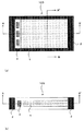
本発明の導光体ユニットを適用したバックライトユニット100について説明する。図1(a)は、本発明の導光体ユニットを適用したバックライトユニット100の平面図を示す。また、図1(b)は、図1(a)に示したバックライトユニットA−A’の断面図である。図3(c)は、図1(a)に示したバックライトユニットB−B’の断面図である。
【0035】
図1に示すように、バックライトユニット100は、大別して、導光体1、ホルダー2、光源として動作するLED(発光ダイオード)3、図示していない反射フィルムなどで構成されている。上記LED3には、図示していないが、各LED3を点灯するための制御回路が接続されている。
【0036】
また、図3(c)に示すように、導光体ユニット200は、導光体1、ホルダー2で構成されている。
【0037】
本実施形態は、エッジライト方式にて、詳細を説明する。しかし、本発明の導光体ユニットの適用は、エッジライト方式だけに限定されず、例えば、フロントライト方式などにも使用可能である。
【0038】
バックライトユニット100は、導光体1の一端面に、LED3を取り付けてなる。また、導光体1の面上には大小の凹凸状の窪みからなる光拡散部が複数形成されている。なお、導光体1の材料は、例えば、ポリメチルメタクリレート(PMMA)樹脂や、ポリカーボネイト(PC)樹脂などの透明性樹脂から形成されている。ポリメチルメタクリレート樹脂は、透明性に優れる代表的な高分子材料であり、その光弾性係数や複屈折は比較的小さく、成形時の残留応力や流動配向が成形品の光学特性に与える影響は小さい。また、ポリカーボネイト樹脂は、ガラス転移温度が145℃と比較的耐熱性に優れた材料である。
【0039】
LED3が導光体1の一端部に設けられた状態で、制御回路により各LEDが発光すると、LED3から導光体1の一端部より入射した光は、導光体内部を導光し、外部に均一に出射する。すなわち、LED3からの入射光は、導光体1の表面へ出射され、液晶表示パネルに光を照射することができる。
【0040】
従来技術では、導光体とホルダーは、個別部品として射出成形される。そして、最終的に組み立て段階でホルダーに導光体を勘合させることで、製品化している。しかし、上述したような従来技術では、導光体とホルダーの隙間には、空気層が介在している。そのため、導光体端面から入射した光は導光体内部を導光し、ほとんどの光は、導光体の出射表面へ出射されるが、一部の光は、導光体端面から出射されてしまうという欠点がある。したがって、従来技術では、光利用効率の点で問題がある。
【0041】
導光体ユニット200は、上記導光体1と上記ホルダー2において、多色成形、例えば、二色成形により一体化成形を実施している。つまり、上記導光体ユニットは、LED3から入射した光を導光体内部に導光させながら、全ての光を液晶表示パネル側に均一に出射させることが可能となる。したがって、従来技術のように、導光体と、導光体を保持するホルダーの隙間に空気層が介在しないため、一部の光が導光体端面から出射されない。要するに、LED3から導光体内部に入射した光の利用効率が向上するのである。
【0042】
また、導光体1の材料とホルダー2の材料は、異なる材料を使用している。上述したように、導光体1の材料は、例えば、ポリメチルメタクリレート(PMMA)樹脂や、ポリカーボネイト(PC)樹脂などの透明性樹脂から形成されている。また、本実施形態のホルダー2の材料は、光源の波長分散に対して、高反射特性を有する樹脂材料を用いる。例えば、ベースの樹脂材料、例えば、ポリカーボネイト樹脂に酸化チタン粉末等を一定割合で混合した、高反射特性を有する樹脂材料を使用する。上記樹脂材料の反射特性は、95%以上の高い値を示す。
【0043】
LED3からの入射光は、導光体内部を導光し、導光体の出射面から出射し、液晶表示パネルを照射する。または、上記入射光は、ホルダー2の材料が高反射特性を有する樹脂材料を用いているため、導光体1とホルダー2の界面で、反射し、再び導光体内部を導光して、導光体の表面に配置されている液晶表示パネルを照射することができるのである。要するに、上記バックライトユニット100を用いることにより、LED3の光利用効率は、さらに向上するのである。
【0044】
導光体ユニット200は、導光体1とホルダー2が一体化しており、また、ホルダー2の樹脂材料は、高反射特性を有している。したがって、バックライトユニット100におけるLED3からの出射光は、導光体と、導光体を保持するホルダーの隙間より光が一部漏れてしまうことは発生せず、導光体1とホルダー2の界面で反射し、再び導光体内部を導光し、最後に導光体1の表面から出射していく。つまり、バックライトユニット100は、LED3からの入射光を、効率良く使用し、液晶表示パネルを照射することができる。
【0045】
したがって、本発明は、光利用効率の高いバックライトユニット100を提供することができる。
【0046】
(バックライトユニットの製造方法)
図2は、本実施形態によるバックライトユニット100の製造工程であり、射出成形機による導光体ユニット200の製造について、詳細を示す。図3(a)、(b)、(c)は、導光体ユニット200の主要製造工程の図を示す。図3(a)、(b)は、射出成形機の重要なツールである金型の断面図である。また、図3(c)は、射出成形により作製される導光体ユニット200であり、また、図1(a)に示すバックライトユニットB−B’の断面図に相当する。
【0047】
バックライトユニット100の製造工程は、大別して3つの工程に分けることができる。工程Paは、導光体ユニット200の製造工程であり、工程Pbは、LED3を搭載した基板の製造工程であり、工程Pcは、導光体ユニット200とLED3を搭載した基板の組み込み工程である。
【0048】
以下に、本発明の重要な工程にあたる工程Pa、つまり、導光体ユニット200の製造工程について、詳細を記す。
【0049】
2本のシリンダーを有する専用の二色成形機を用いた、二色成形法の射出成形による、導光体ユニット200の製造工程を説明する。しかし、導光体ユニット200の製造方法は、2本のシリンダーを有する専用の二色成形機による製造方法のみに限定されるものでなく、例えば、射出成形機を2台用いることによって、一体化成形を実施しても良い。
【0050】
図2に示す射出成形機による導光体ユニット200の製造工程は、インラインスクリュー式射出成形機を用いた場合について説明する。
【0051】
工程Pa1では、型閉を実施する。つまり、型を低圧で、異物のないことを確かめたうえ金型を閉じる。この金型は、固定型51と回転型52から形成されている。次に工程Pa2では、金型を高圧で締め、射出圧力で開かないように型締めを実施する。
【0052】
工程Pa3では、第1シリンダー内のホルダー2の材料に該当する樹脂材料を金型内に高圧・高速で注入し、射出を行う。工程Pa4では、射出シリンダー内の圧力を高圧に保持する。次に工程Pa5では、第1シリンダー内の圧力を下げ、金型内の樹脂材料を固化させる。上記工程Pa3からPa5によって、図3(a)に示すように、ホルダー2が成形される。
【0053】
ホルダー2が成形された後、工程Pa6で、金型の回転型52が回転する。
【0054】
工程Pa7では、第2シリンダー内の導光体1の材料に該当する樹脂材料を金型内に高圧・高速で注入し、射出する。工程Pa8では、第2シリンダー内の圧力を高圧に保持する。次に工程Pa9では、射出シリンダー内の圧力を下げ、金型内のプラスチックを固化させる。上記工程Pa7からPa9によって、図3(b)に示すように、導光体1が成形され、図3(c)に示すように、導光体1とホルダー2が一体化した導光体ユニット200が形成される。上記導光体ユニット200には、光源であるLEDを搭載した基板を組み込む空間が金型により形成されている。
【0055】
次に、工程Pa10により、金型を開き、工程Pa11で、導光体ユニット200を金型からはずす。
【0056】
工程Pcでは、上記工程Paで成形された導光体ユニット200と、工程Pbで実装されたLED搭載基板とが、組み込まれ、本発明によるバックライトユニット100が製造される。
【0057】
本実施形態による導光体ユニット200は、導光体1とホルダー2が一体化しており、また、ホルダー2の材料は、高反射特性も有している。要するに、従来技術のように、導光体と、導光体を保持するホルダーの隙間より光が一部出射されることは発生しない。したがって、バックライトユニット100の光源であるLED3から、導光体1に入射した光は、導光体1とホルダー2の界面に至ると反射し、再び導光体内部を導光し、導光体1の出射表面から出射していく。つまり、バックライトユニット100は、光源からの入射光を、効率良く使用し、液晶表示パネルを照射することができる。
【0058】
したがって、本発明は、光利用効率の高いバックライトユニット100を提供することができる。
【0059】
(液晶表示装置)
図4に本実施形態を用いた液晶表示装置400の断面図を示す。液晶表示装置400は、大きく分けて液晶表示パネル300とバックライトユニット100で構成されている。
【0060】
まず、液晶表示パネル300の構成について説明する。
【0061】
ガラスなどの絶縁性基板4a、4bの表面に透明電極膜5a、5bがそれぞれ形成されると共に、液晶分子を一定の方向に配向させる図示しない配向膜がさらに設けられる。2枚の絶縁性基板4a、4bは、図示しないスペーサーにより一定の間隔を保持しながら、上述の透明電極膜5a、5bが対向するように、その周囲をシール材11により貼着される。2枚の絶縁性基板4a、4bの隙間に液晶材料が封入されることにより、液晶層6が2枚の絶縁性基板4a、4bにより挟持される。さらに、絶縁性基板4a、4bの外側には、それぞれ偏光板7a、7bや位相差板8a、8bが貼着され、これらにより液晶表示パネル300が形成されている。
【0062】
なお、絶縁性基板4aには、スイッチング素子などが形成されていても良いし、また、絶縁性基板4bには、カラーフィルタ9a、9b、9cや保護膜10などが形成されていても良い。
【0063】
上記透明電極膜5a、5bに電圧が印加されることにより、その間に挟持されている液晶分子の配列が変化し、偏光板7a、7bの吸収軸の方向と共にバックライトユニット100からの光の透過および不透過が制御され、所望の表示を得ることができる。
【0064】
本実施形態によるバックライトユニット100は、上述したように、導光体1とホルダー2が一体化しており、また、ホルダー2の材料は、高反射特性も有している。要するに、従来技術のように、導光体と、導光体を保持するホルダーの隙間より光が一部出射されることは発生しない。LED3からの入射した光は、導光体とホルダーの界面に至ると反射し、再び導光体内部を導光し、導光体の出射表面から出射していく。つまり、バックライトユニット100は、LED3からの入射光を、効率良く使用し、液晶表示パネル300を照射することができる。
【0065】
したがって、本実施形態のバックライトユニット100は、明るく表示品位の高い液晶表示装置400を提供することができる。
【0066】
[液晶表示パネルの製造方法]
次に、図4に示した液晶表示パネル300を製造する方法について、図5を参照して説明する。図5は、液晶表示パネル300の製造工程を示すフローチャートである。
【0067】
まず、基板4aを製作し(工程S1)、透明導電膜5aをスパッタリング法により成膜し、フォトリソグラフィ方式によってパターニングを実施し、透明電極膜5aを形成する(工程S2)。さらに透明電極膜5a上に図示しない配向膜を形成し、ラビング処理などを施す(工程S3)。
【0068】
一方、基板4bが製造する(工程S4)。さらに、カラーフィルタ赤9a、カラーフィルタ緑9b、カラーフィルタ青9cの上に設けられたオーバーコート層10の上に透明導電膜5bをスパッタリング法により成膜し、フォトリソグラフィ方式によってパターニングを実施し、透明電極膜5bを形成する(工程S5)。その後、透明電極膜5b上に図示しないポリイミド樹脂などからなる配向膜を形成し、ラビング処理などを施す(工程S6)。
【0069】
そして、シール材11を介して、上記の基板4aと基板4bを貼り合わせて、パネル構造を構成する(工程S7)。基板4aと基板4bとは、基板間に分散配置された図示しないスペーサーなどによって、ほぼ規定の基板間隔となるように貼り合わせられる。
【0070】
その後、シール材11の図示しない開口部から液晶6を封入し、シール材の開口部を紫外線硬化性樹脂などの封止材によって封止する(工程S8)。こうして主要なパネル構造が完成した後に、位相差板8a、8bや偏光板7a、7b等を必要に応じてパネル構造の外面上に貼着などの方法によって取り付け(工程S9)、図4に示す液晶表示パネル300が完成する。
【0071】
[電子機器]
図6は、本実施形態の全体構成を示す概略構成図である。ここに示す電子機器は、上記の液晶表示装置400と、これを制御する制御手段410を有する。ここでは、液晶表示装置400を、パネル構造体400Aと、半導体ICなどで構成される駆動回路400Bとに概念的に分けて描いてある。また、制御手段410は、表示情報出力源411と、表示情報処理回路412と、電源回路413と、タイミングジェネレータ414と、を有する。
【0072】
表示情報出力源411は、ROM(Read Only Memory)やRAM(Random Access Memory)などからなるメモリと、磁気記録ディスクや光記録ディスクなどからなるストレージユニットと、デジタル画像信号を同調出力する同調回路とを備え、タイミングジェネレータ414によって生成された各種のクロック信号に基づいて、所定フォーマットの画像信号などの形で表示情報を表示情報処理回路412に供給するように構成されている。
【0073】
表示情報処理回路412は、シリアル−パラレル変換回路、増幅・反転回路、ローテーション回路、ガンマ補正回路、クランプ回路などの周知の各種回路を備え、入力した表示情報の処理を実行して、その画像情報をクロック信号CLKとともに駆動回路400Bへ
供給する。駆動回路400Bは、走査線駆動回路、データ線駆動回路及び検査回路を含む。また、電源回路413は、上述の各構成要素にそれぞれ所定の電圧を供給する。
【0074】
次に、本発明に係る液晶表示装置を適用可能な電子機器の具体例について図7を参照して説明する。
【0075】
まず、本発明に係る液晶表示装置を、可搬型のパーソナルコンピュータ(いわゆるノート型パソコン)の表示部に適用した例について説明する。図7(a)は、このパーソナルコンピュータの構成を示す斜視図である。同図に示すように、パーソナルコンピュータ510は、キーボード511を備えた本体部512と、本発明に係る液晶表示装置を適用した表示部513とを備えている。
【0076】
続いて、本発明に係る液晶表示装置を、携帯電話機の表示部に適用した例について説明する。図7(b)は、この携帯電話機の構成を示す斜視図である。同図に示すように、携帯電話機520は、複数の操作ボタン521のほか、受話口522、送話口523とともに、本発明に係る液晶表示装置を適用した表示部524を備える。
【0077】
なお、本発明に係る液晶表示パネルを適用可能な電子機器としては、図7(a)に示したパーソナルコンピュータや図7(b)に示した携帯電話機の他にも、液晶テレビ、ビューファインダ型・モニタ直視型のビデオテープレコーダ、カーナビゲーション装置、ページャ、電子手帳、電卓、ワードプロセッサ、ワークステーション、テレビ電話、POS端末、ディジタルスチルカメラなどが挙げられる。
【0078】
[変形例]
また、本発明の電気光学装置は、パッシブマトリクス型の液晶表示パネルだけではなく、アクティブマトリクス型の液晶表示パネル(例えば、TFT(薄膜トランジスタ)やTFD(薄膜ダイオード)をスイッチング素子として備えた液晶表示パネル)にも同様に適用することが可能である。また、液晶表示パネルだけでなく、エレクトロルミネッセンス装置、有機エレクトロルミネッセンス装置、プラズマディスプレイ装置、電気泳動ディスプレイ装置、フィールド・エミッション・ディスプレイ(電界放出表示装置)などの各種の電気光学装置においても本発明を同様に適用することが可能である。
【図面の簡単な説明】
【図1】 (a)本発明に係るバックライトユニットの平面図を示す。
(b)本発明に係るバックライトユニットの断面図を示す。
【図2】 本発明に係るバックライトユニット製造工程を示す。
【図3】 本発明に係る導光体ユニットの製造工程時の断面図を示す。
【図4】 本発明を適用した液晶表示装置の構造を示す断面図である。
【図5】 本発明を適用した液晶表示パネルの製造工程を示す図である。
【図6】 本発明を適用した液晶表示装置を利用する電子機器の構成を示す。
【図7】 本発明を適用した液晶表示装置を備えた電子機器の例を示す。
【符号の説明】
1 導光体
2 ホルダー
3 LED
51 固定型
52 回転型
100 バックライトユニット
200 導光体ユニット
300 液晶表示パネル
400 液晶表示装置[0001]
BACKGROUND OF THE INVENTION
The present invention relates to a backlight unit used in a portable small-sized television, a pager, a wall-mounted television, a notebook computer, an electro-optical device of a portable game machine, and the like, a light guide unit therefor, and an electro-optical device including the backlight unit About.
[0002]
[Background]
In recent years, thin and light liquid crystal display devices have been widely used in display units of portable small-sized televisions, pagers, wall-mounted televisions, notebook computers, portable game machines, and all other electronic devices, and the demand for these devices is increasing. There is a tendency.
[0003]
A reflective liquid crystal display device, which is light, thin, and has low power consumption, does not have a light source unit, and performs display visual recognition using only external light. However, in consideration of use in various environments including outdoors and dark places at night, a reflective liquid crystal display device having a front light type backlight unit and a transmission having an edge light type or area light type backlight unit. Type liquid crystal display devices and transflective liquid crystal display devices have also been developed.
[0004]
The area light type backlight unit is a type in which a light source is arranged directly below a surface light source. An advantage of the area light type backlight unit is that, for example, a large number of cold cathode fluorescent lamps can be arranged in a plane, so that a surface light source with high luminance can be constructed. However, there is a problem that luminance spots and chromaticity spots accompanying the deterioration of the lamp are easily recognized and the backlight unit becomes thick.
[0005]
The edge light type backlight unit is a type in which a light source is arranged on a side surface, and is designed to uniformly guide light to a display unit with a light guide (for example,
[0006]
As described above, the edge light type backlight unit is provided with the light guide. In the light guide, it is important that light incident from a light source such as a cold cathode fluorescent lamp or LED (light emitting diode) is uniformly emitted from the entire emission surface while light is guided into the light guide. It is.
[0007]
Therefore, the optical design of the light source and the light guide is one of important development items because it greatly affects the display quality of electro-optical devices such as liquid crystal display devices.
[0008]
[Patent Document 1]
JP 2001-52520 (
[Patent Document 2]
JP 2002-133907 (5th page, FIG. 1)
[Problems to be solved by the invention]
In electro-optical devices such as liquid crystal display devices, development of various portable devices has been promoted, and demands for higher brightness, thinner thickness, and lower power consumption are increasing. Since the liquid crystal display device itself does not emit light, in general, a configuration in which a backlight unit is arranged in the liquid crystal display device is often employed so that the display can be seen in a dark place.
[0009]
The backlight unit includes an area light type backlight unit and an edge light type backlight unit used in a transmissive liquid crystal display device and a transflective liquid crystal display device, and a front light type backlight unit used in a reflective liquid crystal display device. Etc. The light emitted from the backlight unit is transmitted through the liquid crystal display device, so that the display of the liquid crystal display device can be seen even in a dark place.
[0010]
The edge light type backlight unit described above is provided with a light guide. The function of the light guide is to emit light uniformly from the entire emission surface while guiding light incident from the light source into the light guide.
[0011]
Originally, it is ideal that 100% of the light incident from the light source is emitted to the emission surface on the liquid crystal display panel side while guiding the inside of the light guide. However, at present, this is not realized, and in most cases, light is partly from the end of the light guide that is not on the liquid crystal display panel side, that is, the gap between the light guide and the holder that holds the light guide. It will be emitted. This is because the light guide and the holder holding the light guide are molded as individual parts, and finally the light guide and the holder are fitted in the assembly stage. That is, since there is an air layer in the gap between the light guide and the holder, light incident on the light guide from the light source partially leaks from the end of the light guide to the air layer. Therefore, the conventional light guide unit has a problem that the light use efficiency is not improved.
[0012]
SUMMARY An advantage of some aspects of the invention is that it provides an electro-optical device with high display quality by using a light guide unit that improves light use efficiency of a light source.
[0013]
[Means for Solving the Problems]
The backlight unit of the present invention includes a light guide, a light source disposed to face an incident end face of the light guide, a substrate on which the light source is mounted, A holder disposed at an edge of the light guide, and The light guide is formed smaller than the thickness of the holder, an incident end surface of the light guide is formed away from the holder, and an end surface other than the incident end surface of the light guide is the holder. The light source is disposed between the incident end face of the light guide and the holder, and the substrate on which the light source is mounted is surrounded by one surface of the light guide and the holder Built into the confined space . In the conventional technique, light incident on the light guide from the light source may partially leak into the air layer that exists in the gap between the light guide and the holder. However, by using the integrated light guide unit, light that has partially leaked does not leak, so the light utilization rate by the light guide is improved.
[0014]
In the light guide unit, the light guide and the holder can be integrally formed by, for example, multicolor molding or insert molding means.
[0015]
In one mode of the light guide unit, the material of the holder is different from the material of the light guide. The light guide material is made of, for example, a transparent resin such as a polymethyl methacrylate (PMMA) resin or a polycarbonate (PC) resin.
[0016]
In another aspect of the light guide unit, the holder can be made of a resin material having high reflection characteristics with respect to wavelength dispersion of a light source. By using a material having a high reflection property as the material of the holder, when the light emitted from the light source reaches the interface between the light guide and the holder, the light is guided again inside the light guide. It exits from the exit surface of the body. Therefore, the light use efficiency of the light guide unit is improved.
[0017]
In still another embodiment of the light guide unit, the resin material is mixed with, for example, titanium oxide. The resin material can have a high reflection characteristic of 95% or more, for example, by mixing a certain proportion of titanium oxide.
[0018]
In another aspect of the present invention, the backlight unit can include the light guide unit and a light source. By mounting the light guide unit on the backlight unit, a high-luminance backlight unit with high light utilization efficiency can be provided.
[0019]
In one aspect of the backlight unit, the light source is disposed at an end face where the light guide and the holder are not integrated, for example, between the light guide and the holder.
[0020]
In another aspect of the backlight unit, the light source may be, for example, an LED (light emitting diode).
[0021]
The electro-optical device may include the backlight unit and an electro-optical display panel disposed at a position where the light emitted from the backlight unit is emitted. The electro-optic display panel is, for example, a liquid crystal panel, such as STN (Super Twisted Nematic) mode, TFT-LCD (Thin Film Transistor-Liquid Crystal Display) mode, TFD-LCD (Thin Film Dynode-Liquid Crystal Display) mode, and the like. May be used.
[0022]
Furthermore, according to the present invention, an electronic apparatus can be configured by including the electro-optical device as a display unit.
[0023]
Further, the present invention is a method for manufacturing a backlight unit comprising a light guide, a light source disposed to face the incident end face of the light guide, and a holder disposed at an edge of the light guide, A first step of molding a resin material into the holder; and after the first step, An incident end face of the light guide is formed apart from the holder, and end faces other than the incident end face are integrated with the holder. A second step of forming the light guide so as to After the second step, the light source includes a third step of disposing the light source between the incident end face of the light guide and the holder. In the second step, the light guide The substrate is formed to be smaller than the thickness of the holder, and in the third step, a substrate on which the light source is mounted is incorporated into a space surrounded by one surface of the light guide and the holder. By using the integrated light guide unit, light that has partially leaked does not leak, so the light utilization rate by the light guide improves. The manufacturing method of the light guide unit may be, for example, a manufacturing method using a dedicated two-color molding machine having two cylinders, or a manufacturing method using two injection molding machines.
[0024]
DETAILED DESCRIPTION OF THE INVENTION
Preferred embodiments of the present invention will be described below with reference to the drawings.
[0025]
The present embodiment relates to a light guide unit and a backlight unit that can efficiently use light from a light source. Hereinafter, although this embodiment is described in detail, the scope of the present invention is not limited to the examples described below.
[0026]
[Embodiment]
The present embodiment relates to a light guide unit and a backlight unit installed below a liquid crystal display device. In this embodiment, in order to prevent an air layer from intervening between the light guide in the backlight unit and the holder for holding the light guide, integrated molding is performed by an injection molding method such as a two-color molding method. It is characterized by doing.
[0027]
(Two-color molding method)
Two-color molding is a kind of injection molding method.
[0028]
First, the injection molding will be described below.
[0029]
Injection molding is the most widely used method for plastic molding. The most important tool in the injection molding method is an injection mold. In other words, an injection molding machine is used to perform injection molding, and a plastic molded product having a desired shape is manufactured by a mold attached to the heart of the injection molding machine.
[0030]
The injection molding machine includes a mechanism that melts and injects a plastic material, a mechanism that opens and closes a mold, and a mechanism that controls driving thereof. A general process of the injection molding method will be described. First, granular or pelletized plastic material falls from the hopper to the heating cylinder. The material plasticized by the shearing action by the rotation of the screw is accumulated on the nozzle side, and the screw moves backward in the cylinder and measures the required amount. The plasticized material is then injected into the mold by rapid advancement of the screw. When cooling is completed, the mold is opened, the molded product is taken out, and the process is completed.
[0031]
Next, two-color molding (multicolor) molding will be described below.
[0032]
Two-color (multicolor) molding is a method of simultaneously molding letters, numbers, symbols, etc. of different colors on an injection molded product, for example. The above two-color (multicolor) molding method requires two or more injection molding machines or a dedicated two-color (multicolor) molding machine having two or more cylinders, and the mold also rotates, A special mold that expands is required.
[0033]
In the present embodiment, a light guide unit produced by a dedicated two-color molding machine having two cylinders will be described. However, the present embodiment is not limited to a dedicated two-color molding machine having two cylinders, and for example, integral molding may be performed by using two or more injection molding machines. .
[0034]
(Backlight unit structure)
The
[0035]
As shown in FIG. 1, the
[0036]
In addition, as shown in FIG. 3C, the
[0037]
This embodiment will be described in detail using an edge light system. However, the application of the light guide unit of the present invention is not limited to the edge light system, and can be used for a front light system, for example.
[0038]
The
[0039]
When each LED emits light by the control circuit in a state where the
[0040]
In the prior art, the light guide and the holder are injection molded as separate parts. And finally, it is commercialized by fitting the light guide to the holder in the assembly stage. However, in the conventional technology as described above, an air layer is interposed in the gap between the light guide and the holder. Therefore, the light incident from the end face of the light guide is guided through the inside of the light guide, and most of the light is emitted to the exit surface of the light guide, but some light is emitted from the end face of the light guide. There is a disadvantage that it ends up. Therefore, the conventional technique has a problem in light utilization efficiency.
[0041]
In the
[0042]
Moreover, the material of the
[0043]
Incident light from the
[0044]
In the
[0045]
Therefore, the present invention can provide the
[0046]
(Backlight unit manufacturing method)
FIG. 2 is a manufacturing process of the
[0047]
The manufacturing process of the
[0048]
Details of the process Pa corresponding to the important process of the present invention, that is, the manufacturing process of the
[0049]
A manufacturing process of the
[0050]
The manufacturing process of the
[0051]
In step Pa1, mold closing is performed. In other words, the mold is closed after confirming that the mold is at a low pressure and that there is no foreign matter. This mold is formed of a fixed
[0052]
In step Pa3, a resin material corresponding to the material of the
[0053]
After the
[0054]
In step Pa7, a resin material corresponding to the material of the
[0055]
Next, at step Pa10, the mold is opened, and at step Pa11, the
[0056]
In the process Pc, the
[0057]
In the
[0058]
Therefore, the present invention can provide the
[0059]
(Liquid crystal display device)
FIG. 4 shows a cross-sectional view of a liquid
[0060]
First, the configuration of the liquid
[0061]
[0062]
Note that a switching element or the like may be formed on the insulating
[0063]
When a voltage is applied to the
[0064]
As described above, in the
[0065]
Therefore, the
[0066]
[Method of manufacturing liquid crystal display panel]
Next, a method for manufacturing the liquid
[0067]
First, a
[0068]
On the other hand, the
[0069]
And the said board |
[0070]
Thereafter, the
[0071]
[Electronics]
FIG. 6 is a schematic configuration diagram showing the overall configuration of the present embodiment. The electronic apparatus shown here includes the liquid
[0072]
The display
[0073]
The display
Supply. The driving
[0074]
Next, specific examples of electronic devices to which the liquid crystal display device according to the present invention can be applied will be described with reference to FIG.
[0075]
First, an example in which the liquid crystal display device according to the present invention is applied to a display unit of a portable personal computer (so-called notebook personal computer) will be described. FIG. 7A is a perspective view showing the configuration of this personal computer. As shown in the figure, the
[0076]
Next, an example in which the liquid crystal display device according to the present invention is applied to a display unit of a mobile phone will be described. FIG. 7B is a perspective view showing the configuration of the mobile phone. As shown in the figure, a
[0077]
Note that, as an electronic device to which the liquid crystal display panel according to the present invention can be applied, in addition to the personal computer shown in FIG. 7A and the mobile phone shown in FIG. Monitor direct-view video tape recorders, car navigation devices, pagers, electronic notebooks, calculators, word processors, workstations, videophones, POS terminals, digital still cameras, etc.
[0078]
[Modification]
The electro-optical device of the present invention is not limited to a passive matrix type liquid crystal display panel, but also an active matrix type liquid crystal display panel (for example, a TFT (thin film transistor) or a TFD (thin film diode)) as a switching element. ) Can be applied in the same manner. In addition to the liquid crystal display panel, the present invention is applied to various electro-optical devices such as an electroluminescence device, an organic electroluminescence device, a plasma display device, an electrophoretic display device, and a field emission display (field emission display device). It is possible to apply similarly.
[Brief description of the drawings]
FIG. 1A is a plan view of a backlight unit according to the present invention.
(B) A sectional view of a backlight unit according to the present invention is shown.
FIG. 2 shows a backlight unit manufacturing process according to the present invention.
FIG. 3 is a cross-sectional view of the light guide unit according to the present invention during the manufacturing process.
FIG. 4 is a cross-sectional view showing a structure of a liquid crystal display device to which the present invention is applied.
FIG. 5 is a diagram showing a manufacturing process of a liquid crystal display panel to which the present invention is applied.
FIG. 6 illustrates a structure of an electronic device using a liquid crystal display device to which the present invention is applied.
FIG. 7 illustrates an example of an electronic device including a liquid crystal display device to which the present invention is applied.
[Explanation of symbols]
1 Light guide
2 Holder
3 LED
51 Fixed type
52 Rotating type
100 backlight unit
200 Light guide unit
300 LCD panel
400 Liquid crystal display device
Claims (8)
前記導光体の入射端面に対向して配置された光源と、
前記光源を搭載した基板と、
前記導光体の縁部に配置されたホルダーと、を備え、
前記導光体は、前記ホルダーの厚みよりも小さく形成されており、前記導光体の入射端面が前記ホルダーと離間して形成されると共に、前記導光体の入射端面以外の端面が前記ホルダーと一体化されており、
前記光源が、前記導光体の入射端面と前記ホルダーとの間に配置され、
前記光源を搭載した基板が、前記導光体の一方の面と前記ホルダーとで囲まれた空間に組み込まれてなることを特徴とするバックライトユニット。 A light guide;
A light source disposed to face the incident end face of the light guide;
A substrate on which the light source is mounted;
A holder disposed at an edge of the light guide, and
The light guide is formed smaller than the thickness of the holder, an incident end surface of the light guide is formed away from the holder, and an end surface other than the incident end surface of the light guide is the holder. Is integrated with
The light source is disposed between the incident end face of the light guide and the holder;
A backlight unit, wherein a substrate on which the light source is mounted is incorporated in a space surrounded by one surface of the light guide and the holder .
前記バックライトユニットからの出射光が出射される位置に配置された電気光学表示パネルと、を備えることを特徴とする電気光学装置。The backlight unit according to any one of claims 1 to 5 ,
An electro-optical device comprising: an electro-optical display panel disposed at a position where light emitted from the backlight unit is emitted.
樹脂材料を前記ホルダーに成形する第1の工程と、
前記第1の工程後、前記導光体の入射端面を、前記ホルダーと離間して形成すると共に、前記入射端面以外の端面を、前記ホルダーと一体化するように前記導光体を成形する第2の工程と、
前記第2の工程後、前記光源を、前記導光体の入射端面と前記ホルダーとの間に配置する第3の工程とを有し、
前記第2の工程において、前記導光体は、前記ホルダーの厚みよりも小さく形成し、
前記第3の工程において、前記導光体の一方の面と前記ホルダーとで囲まれた空間に、前記光源を搭載した基板を組み込むことを特徴とするバックライトユニットの製造方法。 A method for manufacturing a backlight unit comprising a light guide, a light source disposed opposite to an incident end face of the light guide, and a holder disposed at an edge of the light guide,
A first step of molding the resin material in the holder,
After the first step, the incident end face of the light guide, with formed apart from the holder, the end surface other than the incident end face, the shaping of the light guide body so as to integrate with the holder Two steps;
A third step of disposing the light source between the incident end surface of the light guide and the holder after the second step;
In the second step, the light guide is formed smaller than the thickness of the holder,
The method of manufacturing a backlight unit, wherein in the third step, a substrate on which the light source is mounted is incorporated in a space surrounded by one surface of the light guide and the holder.
Priority Applications (1)
| Application Number | Priority Date | Filing Date | Title |
|---|---|---|---|
| JP2002258873A JP4232417B2 (en) | 2002-09-04 | 2002-09-04 | Backlight unit, electro-optical device, electronic apparatus, and method for manufacturing backlight unit |
Applications Claiming Priority (1)
| Application Number | Priority Date | Filing Date | Title |
|---|---|---|---|
| JP2002258873A JP4232417B2 (en) | 2002-09-04 | 2002-09-04 | Backlight unit, electro-optical device, electronic apparatus, and method for manufacturing backlight unit |
Publications (3)
| Publication Number | Publication Date |
|---|---|
| JP2004095516A JP2004095516A (en) | 2004-03-25 |
| JP2004095516A5 JP2004095516A5 (en) | 2005-10-06 |
| JP4232417B2 true JP4232417B2 (en) | 2009-03-04 |
Family
ID=32063386
Family Applications (1)
| Application Number | Title | Priority Date | Filing Date |
|---|---|---|---|
| JP2002258873A Expired - Fee Related JP4232417B2 (en) | 2002-09-04 | 2002-09-04 | Backlight unit, electro-optical device, electronic apparatus, and method for manufacturing backlight unit |
Country Status (1)
| Country | Link |
|---|---|
| JP (1) | JP4232417B2 (en) |
Cited By (1)
| Publication number | Priority date | Publication date | Assignee | Title |
|---|---|---|---|---|
| CN104476719A (en) * | 2014-08-29 | 2015-04-01 | 深圳市德仓科技有限公司 | Injection molding equipment, LCD module, backlight module and manufacturing method thereof |
Families Citing this family (7)
| Publication number | Priority date | Publication date | Assignee | Title |
|---|---|---|---|---|
| JP2007281260A (en) * | 2006-04-07 | 2007-10-25 | Sumitomo Metal Electronics Devices Inc | Reflector, package for housing light-emitting element using the same, and lens used for reflector |
| JP5083954B2 (en) | 2007-08-23 | 2012-11-28 | シチズン電子株式会社 | Film-shaped light guide plate unit, planar light unit, display device, and electronic apparatus |
| TW201027001A (en) * | 2009-01-06 | 2010-07-16 | Golden Light Technology Corp | Light emitting diode lamp device |
| KR101006838B1 (en) | 2009-04-06 | 2011-01-12 | (주)케이제이 프리테크 | LED backlight is integrally manufactured by light guide panel of curable resin and manufacturing method thereof |
| WO2011132515A1 (en) * | 2010-04-22 | 2011-10-27 | シャープ株式会社 | Illumination device and display device |
| CN104325598A (en) * | 2014-08-29 | 2015-02-04 | 深圳市德仓科技有限公司 | Injection moulding device, liquid crystal module, backlight module and manufacturing method thereof |
| JP2017191879A (en) * | 2016-04-14 | 2017-10-19 | 株式会社小糸製作所 | Light emitting module |
-
2002
- 2002-09-04 JP JP2002258873A patent/JP4232417B2/en not_active Expired - Fee Related
Cited By (1)
| Publication number | Priority date | Publication date | Assignee | Title |
|---|---|---|---|---|
| CN104476719A (en) * | 2014-08-29 | 2015-04-01 | 深圳市德仓科技有限公司 | Injection molding equipment, LCD module, backlight module and manufacturing method thereof |
Also Published As
| Publication number | Publication date |
|---|---|
| JP2004095516A (en) | 2004-03-25 |
Similar Documents
| Publication | Publication Date | Title |
|---|---|---|
| US6657687B2 (en) | Liquid crystal display, manufacturing method thereof, and electronic appliance | |
| US7391484B2 (en) | Electro-optical method of manufacturing spacer light-shielding film simultaneously with switching unit element using same materials and process | |
| US8896800B2 (en) | Liquid crystal panel and liquid crystal display device using the same | |
| US20050259440A1 (en) | Lighting device, liquid crystal display device, and electronic apparatus | |
| US20070035842A1 (en) | Liquid-guide plate, backlight assembly and liquid crystal display having the same | |
| JP2006190679A (en) | Backlight assembly removing dark part and display device including it | |
| KR20140020157A (en) | Liquid crystal display apparatus and method for manufacturing the same | |
| JP4700321B2 (en) | Liquid crystal display panel, liquid crystal display device having the same, and method for manufacturing liquid crystal display panel | |
| US10613381B2 (en) | Diffusion plate and direct-type backlight module | |
| US20060290852A1 (en) | Transflective LCD device with enhanced light transmittance | |
| WO2009081534A1 (en) | Liquid crystal display panel, liquid crystal display device and manufacturing method of liquid crystal display panel | |
| JP2018081192A (en) | Liquid crystal display device and method for manufacturing liquid crystal display device | |
| JP4232417B2 (en) | Backlight unit, electro-optical device, electronic apparatus, and method for manufacturing backlight unit | |
| KR20060083894A (en) | Liquid crystal display device | |
| JP4178968B2 (en) | BACKLIGHT UNIT, ELECTRO-OPTICAL DEVICE, ELECTRONIC DEVICE, METHOD FOR PRODUCING BACKLIGHT UNIT, AND METHOD FOR MANUFACTURING ELECTRO-OPTICAL DEVICE | |
| JP2000267077A (en) | Liquid crystal display device and electronic equipment | |
| US20060044494A1 (en) | Transflective liquid crystal display device and manufacturing method for the same | |
| JP4125746B2 (en) | Backlight device and liquid crystal display device | |
| KR20060133821A (en) | Backlight assembly and liquid crystal display comprising the same | |
| KR20070044136A (en) | Back-light assembly and liquid crystal display apparatus having the same | |
| JP2004103333A (en) | Backlight unit, electro-optic device, electronic apparatus, and manufacturing method of backlight unit | |
| KR102082679B1 (en) | Liquid crystal display device and method for fabricating the same | |
| US20070279943A1 (en) | Backlight assembly, liquid crystal display apparatus having the same and method thereof | |
| JP2004039501A (en) | Backlight unit, electro-optical panel, electro-optical device, electronic apparatus, manufacturing method of light guide plate, and manufacturing method of substrate | |
| JP2006140078A (en) | Lighting device, electro-optical device, and electronic equipment |
Legal Events
| Date | Code | Title | Description |
|---|---|---|---|
| A521 | Written amendment |
Free format text: JAPANESE INTERMEDIATE CODE: A523 Effective date: 20050517 |
|
| A621 | Written request for application examination |
Free format text: JAPANESE INTERMEDIATE CODE: A621 Effective date: 20050517 |
|
| RD04 | Notification of resignation of power of attorney |
Free format text: JAPANESE INTERMEDIATE CODE: A7424 Effective date: 20070402 |
|
| A977 | Report on retrieval |
Free format text: JAPANESE INTERMEDIATE CODE: A971007 Effective date: 20080327 |
|
| A131 | Notification of reasons for refusal |
Free format text: JAPANESE INTERMEDIATE CODE: A131 Effective date: 20080408 |
|
| A521 | Written amendment |
Free format text: JAPANESE INTERMEDIATE CODE: A523 Effective date: 20080605 |
|
| TRDD | Decision of grant or rejection written | ||
| A01 | Written decision to grant a patent or to grant a registration (utility model) |
Free format text: JAPANESE INTERMEDIATE CODE: A01 Effective date: 20081118 |
|
| A01 | Written decision to grant a patent or to grant a registration (utility model) |
Free format text: JAPANESE INTERMEDIATE CODE: A01 |
|
| A61 | First payment of annual fees (during grant procedure) |
Free format text: JAPANESE INTERMEDIATE CODE: A61 Effective date: 20081201 |
|
| FPAY | Renewal fee payment (event date is renewal date of database) |
Free format text: PAYMENT UNTIL: 20111219 Year of fee payment: 3 |
|
| R150 | Certificate of patent or registration of utility model |
Free format text: JAPANESE INTERMEDIATE CODE: R150 |
|
| FPAY | Renewal fee payment (event date is renewal date of database) |
Free format text: PAYMENT UNTIL: 20111219 Year of fee payment: 3 |
|
| FPAY | Renewal fee payment (event date is renewal date of database) |
Free format text: PAYMENT UNTIL: 20121219 Year of fee payment: 4 |
|
| FPAY | Renewal fee payment (event date is renewal date of database) |
Free format text: PAYMENT UNTIL: 20121219 Year of fee payment: 4 |
|
| FPAY | Renewal fee payment (event date is renewal date of database) |
Free format text: PAYMENT UNTIL: 20131219 Year of fee payment: 5 |
|
| LAPS | Cancellation because of no payment of annual fees |