JP4230704B2 - High frequency MOSFET switch - Google Patents
High frequency MOSFET switch Download PDFInfo
- Publication number
- JP4230704B2 JP4230704B2 JP2002031997A JP2002031997A JP4230704B2 JP 4230704 B2 JP4230704 B2 JP 4230704B2 JP 2002031997 A JP2002031997 A JP 2002031997A JP 2002031997 A JP2002031997 A JP 2002031997A JP 4230704 B2 JP4230704 B2 JP 4230704B2
- Authority
- JP
- Japan
- Prior art keywords
- coupled
- node
- transfer transistor
- impedance
- switch circuit
- Prior art date
- Legal status (The legal status is an assumption and is not a legal conclusion. Google has not performed a legal analysis and makes no representation as to the accuracy of the status listed.)
- Expired - Fee Related
Links
Images


Classifications
-
- H—ELECTRICITY
- H03—ELECTRONIC CIRCUITRY
- H03K—PULSE TECHNIQUE
- H03K17/00—Electronic switching or gating, i.e. not by contact-making and –breaking
- H03K17/04—Modifications for accelerating switching
-
- H—ELECTRICITY
- H03—ELECTRONIC CIRCUITRY
- H03K—PULSE TECHNIQUE
- H03K17/00—Electronic switching or gating, i.e. not by contact-making and –breaking
- H03K17/16—Modifications for eliminating interference voltages or currents
- H03K17/161—Modifications for eliminating interference voltages or currents in field-effect transistor switches
- H03K17/162—Modifications for eliminating interference voltages or currents in field-effect transistor switches without feedback from the output circuit to the control circuit
-
- H—ELECTRICITY
- H03—ELECTRONIC CIRCUITRY
- H03K—PULSE TECHNIQUE
- H03K17/00—Electronic switching or gating, i.e. not by contact-making and –breaking
- H03K17/04—Modifications for accelerating switching
- H03K17/041—Modifications for accelerating switching without feedback from the output circuit to the control circuit
- H03K17/0412—Modifications for accelerating switching without feedback from the output circuit to the control circuit by measures taken in the control circuit
- H03K17/04123—Modifications for accelerating switching without feedback from the output circuit to the control circuit by measures taken in the control circuit in field-effect transistor switches
-
- H—ELECTRICITY
- H03—ELECTRONIC CIRCUITRY
- H03K—PULSE TECHNIQUE
- H03K17/00—Electronic switching or gating, i.e. not by contact-making and –breaking
- H03K17/51—Electronic switching or gating, i.e. not by contact-making and –breaking characterised by the components used
- H03K17/56—Electronic switching or gating, i.e. not by contact-making and –breaking characterised by the components used by the use, as active elements, of semiconductor devices
- H03K17/687—Electronic switching or gating, i.e. not by contact-making and –breaking characterised by the components used by the use, as active elements, of semiconductor devices the devices being field-effect transistors
-
- H—ELECTRICITY
- H03—ELECTRONIC CIRCUITRY
- H03K—PULSE TECHNIQUE
- H03K2217/00—Indexing scheme related to electronic switching or gating, i.e. not by contact-making or -breaking covered by H03K17/00
- H03K2217/0018—Special modifications or use of the back gate voltage of a FET
Description
【0001】
【発明の属する技術分野】
本発明は、電子スイッチに関する。特に、本発明は、半導体スイッチに関し、1つ又は複数の金属酸化物半導体電界効果トランジスタ(MOSFET)によって構成されるものを含む。更に詳しくは、本発明は、1ギガヘルツのオーダーの周波数を含む比較的高周波でのスイッチングが可能な半導体スイッチに関する。
【0002】
【従来の技術】
半導体技術の発展により、機械式リレーを効果的に代替する低コストで信頼性の高いスイッチを作成することができるようになっている。そのようなスイッチは、1極1投型のリレーとして実現されるときに特に有用であることがわかっているが、それに限定されることはない。半導体スイッチは、従来の機械式リレーに代わるものとしてますます用いられている。これは、半導体スイッチを用いることによって得られる高いスイッチング速度や、故障なく比較的多くの電流を移動させることができる能力による。これらのスイッチは、転送ゲート(transfer gate)又は通過トランジスタ(pass transistor)と称されることが多い。というのは、信号の通過を許可又は阻止するというトランジスタ(通常はMOSトランジスタ)の特性がそこで用いられているからである。
【0003】
スイッチが多くの分野において用いられていることは広く知られている。スイッチは、非常に多様な大型及び小型の製品で用いられており、例えば、これらに限定されるのではないが、自動車や家庭用電子製品などがその例である。スイッチは、アナログのルータ、ゲート及びリレーとして用いることができ、現にそのようなものとして用いられている。また、デジタルのマルチプレクサ、ルータ及びゲートとしても用いられている。
【0004】
一般的なP型MOSトランジスタ・スイッチが、図1に示されている。このスイッチは、基本的に、ノードAに結合されたソースとノードBに結合されたドレインとを有しノードAとノードBとの間での信号伝送を制御しているPMOSトランジスタM1である。スイッチM1の制御ゲートは、外部制御回路からのイネーブル信号入力ノードENによってイネーブルされる。ENは、一般に、インバータIV1及びIV2などの1つ又は複数のインバータ対を含むインバータ列によってM1のゲートに結合される。インバータIV1及びIV2は、高電位電力レールVccと低電位電力レールGNDとによって給電される。スイッチ・トランジスタのバルク(bulk)は、高電位電力レールに結合される。動作の際は、ENに与えられる論理ローがインバータ列を伝搬してM1をオンさせ、それによって、信号がノードAとノードBとの間を通過することが可能になる。この場合、AからBでも、BからAでもよい。ENに論理ハイが与えられるとM1がオフになり、それによって、ノードAとノードBとの間の信号伝搬が阻止される。
【0005】
本発明についての説明を進めるために、ライン抵抗R1及びR2が示され、また、規制キャパシタンスC1、C2及びC3も示されている。抵抗R1及びR2は、トランジスタ・スイッチ回路に結合された回路に関連するインピーダンスを表す。このインピーダンスは何らかの予測される値を有しているのであるが、例えば、ある応用例では、抵抗R1及びR2は、一般に、約50オームのオーダーである。しかし、本発明が外部回路に関連するどのような特定の負荷インピーダンスにも限定されないことに注意すべきである。
【0006】
更に図1に関する考察を続けるが、キャパシタンスC1はトランジスタ構造のゲート・ソース間のインターフェースに関連するインピーダンスを表し、キャパシタンスC2はトランジスタ構造のドレイン・ゲート間のインターフェースに関連するインピーダンスを表し、キャパシタンスC3はトランジスタ構造のゲート・バルク間のインターフェース(典型的には、ゲート酸化物層)に関連するインピーダンスを表す。N型のMOSを用いて、PMOSトランジスタM1によって与えられるのと同じスイッチング機能を相補的に実行することができることに注意すべきである。ただしその際には、インバータ列を適切に修正し、トランジスタのバルクはVccにではなくGNDに結合される。NMOS及びPMOSトランジスタに関係する技術分野の当業者であれば、このような差異を理解している。
【0007】
MOSトランジスタは、動作電力が極めて小さいという点で望ましい。製造技術が進歩するにつれて、これらの構造が有効に動作する際の供給電位やスイッチング速度は改善されている。しかし、図1に示されているように構成されたほとんどのシリコンMOSトランジスタ・スイッチでは、信号の伝送周波数が400MHzのオーダーを超えると、AB間での信号伝搬に困難が生じることがわかっている。M1のサイズを縮小することによってこの特性を改善することができるように考えられるかもしれないが、トランジスタのオン抵抗値(on-resistance)が増加することを含む望ましくないトレードオフが存在する。トランジスタのオン抵抗値を低く維持するという観点を別としても、この構造の伝達関数を評価する際の正味の結果は、周波数パフォーマンスに関して僅かなゲインしか存在しない、又は、ゲインが全く存在しないというものである。
【0008】
図1に示されたスイッチ・トランジスタのインピーダンスを解析すると、このデバイスに付随する伝搬周波数の限界を理解することができる。特に、例えば、伝送信号の伝搬周波数が300MHzを超えると、抵抗R1及びR2とゲート結合されたキャパシタンスC1、C2及びC3とによって単純に識別されるシステムの特性に関連するインピーダンスが、伝達関数を支配し始める。結果的に、そのような周波数又はそれよりも高い周波数では、Vccに結合されたトランジスタのバルクとGNDとの間に(M1をイネーブルするインバータIV2を介して)シャントすなわち短絡が生じる。上述したように、これは、オン抵抗値を望ましくない程度まで上昇させるM1のゲート・サイズを縮小することによっては、解決することができない。
【0009】
コンピューティングに関するほとんどの応用例では、MOSトランジスタ・スイッチの周波数の限界は、ほとんど関心の対象にはならない。しかし、例えば、ビデオ伝送フィールドなど、動作帯域幅に関する要求が大きくなると、損失を最小に維持しながら比較的高周波での伝送を通過させることができるMOSトランジスタ・スイッチに対する要求が大きくなる。従って、必要であるのは、デジタル及びアナログ動作に対するスイッチとして機能する半導体回路である。やはり必要であるのは、予測される供給電位のアレイ上で転送ゲート又は通過ゲートとして動作することができる半導体スイッチである。更に、必要であるのは、最小の減衰で比較的高周波の信号を伝搬することができるMOSFETベースのスイッチ回路である。更に必要であるのは、トランジスタ回路に関連するオン抵抗値への影響が最小となるように高周波伝送を伝搬するようなスイッチ回路である。
【0010】
【発明の概要】
本発明の目的は、デジタル及びアナログ動作に対するスイッチとして機能する半導体回路を提供することである。本発明の別の目的は、広い範囲の供給電位で動作可能な転送ゲート又は通過ゲートである半導体スイッチを提供することである。本発明の別の目的は、最小の減衰で比較的高周波の信号を伝搬させることができるMOSFETベースのスイッチ回路を提供することである。本発明の別の目的は、MOSFETベースの通過ゲート構造に関連するオン抵抗値への影響が最小となるように高周波伝送を伝搬させるようなスイッチ回路を提供することである。
【0011】
以上の及びそれ以外の目的は、本発明において、通過ゲートを確立するのに用いられる既存のMOSFET構造に関連するシャント経路のインピーダンスを増加させることによって達成される。特に、抵抗素子、容量性素子又はその組合せなどのインピーダンス要素が、通過ゲート・トランジスタのゲートと供給レールとの間に結合される。インピーダンス要素は、通過ゲート・トランジスタのゲートをゲート電位を決定する供給レールから切り離すように機能する。更に、このようなインピーダンス要素は、通過ゲート・トランジスタのバルクとそのバルクが結合されている供給レールとの間に結合して、やはり、通過ゲート・トランジスタのその部分をその特定の供給レールから切り離すこともできる。PMOSトランジスタでは、バルクは高電位レールに直接に結合されるが通常であり、NMOSトランジスタでは、バルクは低電位レールに結合されるのが通常である。通過ゲート・トランジスタとして用いられる従来型のMOSトランジスタ構造では、本発明の回路を通過して伝搬する実質的に減衰されていない信号周波数を少なくとも2倍にするためには、システム自体のインピーダンスよりも大きなインピーダンスが好ましいことがわかっている。もちろん、用いられる特定のインピーダンスは、通過ゲート、関心対象である動作周波数、回路に対する予測される負荷及びそれ以外のファクタの特定の特性の関数として選択することができる。更に、ゼロでないインピーダンスが補完されれば、それによってスイッチの応答性能を向上させることができる。
【0012】
本発明のインピーダンス要素は、通過ゲート・トランジスタの寄生キャパシタンス経路と直列に結合され、それによって、これらの経路の全体的なインピーダンスが増加する。結果的に、これらのキャパシタンス経路が確立していた従来のシャントは実質的に否定される。特に、高周波での伝搬が関心対象であるような状況では、特にそうである。それ以外のすべての点では、本発明による通過ゲート・トランジスタ回路によると、従来型の相補的MOS(CMOS)スイッチ・デバイスに対して予測される信号伝送が可能である。
【0013】
本発明は、高周波スイッチングが関心対象となるような広い範囲の応用例において用いるのに適している。最も根本的なレベルでは、通過ゲート回路は、ある場所から別の場所への個別的な信号の伝搬に影響を与える。通過ゲート回路は、組み合わされることにより、非常に多くの信号を伝搬させるように動作するデータ伝送システムを形成し、ますます複雑な結果を得ることができる。基本的なレベルでは、通過ゲート回路は、デバイスを相互に接続し、ディスクリートなデバイスの間での信号伝搬を可能にするようにデザインされているバスやバックプレーンを形成するのに用いることができる。ローカルな又は内部的なバスは、マイクロプロセッサなどのディスクリートなデバイス内部での信号経路を提供する。マイクロプロセッサ・システムに含まれるローカル・バスのタイプには、ISA、EISA、マイクロ・チャネル、VLバス、PCIバスなどがある。プリンタやキーボードなどの周辺システムを接続するバスの例としては、Nuバス(NuBus)、ターボチャネル(TURBOchannel)、VMEバス(VMEbus)、マルチバス(MULTIBUS)、STDバスなどがある。これらのタイプの信号伝送システムは、それぞれが、それを構成するのに用いられているコンポーネントと同程度にだけ有効に動作することができる。本発明による通過ゲート回路などのような改良型の通過ゲート回路は、これらのバスの任意のものにおいて、そしてプリント回路ボードを相互接続するのに用いられるバックプレーン構造においても、用いることができ、それによって伝搬速度が高速化される。ビデオ及びグラフィクス信号の伝送のために、そして特にフラット・スクリーン・パネルのために、低電圧差動シグナリング(LVDS)、伝送最小化差動シグナリング(TMDS)、非同期転送モード(ATM)、デジタル・ビジュアル・インターフェース(DVI)などのインターフェースが、そのような伝送を可能にするように設計されている。
【0014】
伝搬速度の向上は、高密度の(dense)データ・パケットの高速転送のために特に重要である。ある場所から別の場所までデータ・パケットを送るのに用いられる改良型のルータは、ローカル・エリア・ネットワーク及びワイド・エリア・ネットワークを介してのデータ転送を向上させるために、ますますスイッチ回路に依存するようになっている。これは、高品位のビデオ、グラフィクス、データ及び音声をワイヤード、光及び無線接続によって伝送させる場合に、特にそういえる。そのようなルータは、デバイスの間の信号トラフィックの流れを制御するのに用いられるが、様々な信号伝送プロトコルの認識に依存している。このようなプロトコルには、これは限定を意味するのではないが、IP、IPX、アップルトーク(AppleTalk)、DECネット(DECnet)が含まれる。本発明の回路のような改良型のスイッチング回路によると、そのような信号ルータの動作が容易になり改善される。もちろん、本発明は、パーソナル・コンピュータ、パーソナル・デジタル・デバイス、通信デバイス、高速で高品位の信号伝搬を必要とするそれ以外の電子システムなど、任意のコンピューティング・システムでの使用に適している。
【0015】
本発明のこれらの及びそれ以外の効果は、本発明の実施例に関する以下の詳細な説明、添付の図面及び冒頭の特許請求の範囲を検討することによって、明らかになろう。
【0016】
【発明の実施の形態】
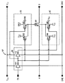
本発明による高周波スイッチ回路10が図2に示されている。回路10は、好ましくは、インバータIV1及びIV2とPMOS通過ゲート・トランジスタM1とで形成されており、これは、図1に示されている従来技術によるスイッチと相当に類似している。もちろん、インバータ段20は、複数のインバータ対や、それ以外の形態のイネーブル信号伝搬機構を用いて形成することもできる。回路10は、また、第1のインピーダンス要素30と第2のインピーダンス要素40とを含んでおり、要素30はインバータ段20の出力とM1のゲートとの間に結合されており、要素40はM1のバルクと高電位電力レールVccとの間に結合されている。出力イネーブル・ノードENによる制御回路(図3に図示せず)からのイネーブル信号は、好ましくは、インバータ段20の入力に結合されて、そのゲートによるトランジスタM1の動作制御を実質的に決定する。インバータIV1及びIV2は、典型的には、高電位レールVccと低電位レールGNDとによって給電される。第1のインピーダンス要素30と別の態様でM1のゲートに結合することもできるが、それは、ゲートを供給レールから切り離すように機能する場合である。第2のインピーダンス要素40の結合に関しても同じことがいえる。
【0017】
トランジスタM1は、ノードAとノードBとの間での信号転送に関する基本的な制御装置(regulator)である。これらの2つのノードに結合された外部回路の間で信号がどちらの方向に流れるかに応じて、ノードA又はノードBのいずれか一方が、入力ノード又は出力ノードにすることができる。要素30及び40は、M1のゲートと段20の出力との間、そして、M1のバルクとVccとの間、のそれぞれに直列のインピーダンスを提供するように設計されている。結果的に得られるのは、比較的高周波である350MHz以上で支配的であったトランジスタM1の寄生キャパシタンスによって従来は特徴付けられていた、比較的高インピーダンスの経路である。
【0018】
同様の高周波スイッチ回路100が、NMOS通過ゲート・トランジスタM2について図3に示されている。回路100は、好ましくは、インバータIV1とNMOS通過ゲート・トランジスタM2とで形成されている。もちろん、インバータ段120は、奇数である複数のインバータや、それ以外の形態のイネーブル信号伝搬機構を用いて形成することもできる。回路100は、また、第1のインピーダンス要素130と第2のインピーダンス要素140とを含んでおり、要素130はインバータ段120の出力とM2のゲートとの間に結合されており、要素140はM2のバルクとGNDとの間に結合されている。出力イネーブル・ノードENによる制御回路(図3に図示せず)からのイネーブル信号は、好ましくは、インバータ段120の入力に結合されて、そのゲートによるトランジスタM2の動作制御を実質的に決定する。インバータIV1は、典型的には、Vcc及びGNDによって給電される。トランジスタM2は、ノードAとノードBとの間での信号転送に関する基本的な制御装置である。これらの2つのノードに結合された外部回路の間で信号がどちらの方向に流れるかに応じて、ノードA又はノードBのいずれか一方が、入力ノード又は出力ノードにすることができる。要素130及び140は、M2のゲートと段120の出力との間、そして、M2のバルクとGNDとの間、のそれぞれに直列のインピーダンスを提供するように設計されている。結果的に得られるのは、比較的高周波である350MHz以上で支配的であったトランジスタM2の寄生キャパシタンスによって従来は特徴付けられていた、比較的高インピーダンスの経路である。
【0019】
図4は、図2に示されているPMOSベースの高周波スイッチ回路の1つの好適実施例を図解している。回路10’は、インバータ段20と、第1のインピーダンス要素30と、第2のインピーダンス要素40と、通過ゲート・トランジスタM1とを含む。インピーダンス要素30は、IV2の出力に結合された高電位ノードとM1のゲートに結合された低電位ノードとを有する抵抗R3を含む。要素30は、更に、そのゲートがインバータIV1の出力に結合され、そのソースがVccに結合され、そのドレインがM1のゲートに結合されたPMOSシャント制御トランジスタM3を含む。インピーダンス要素40は、Vccに結合された高電位ノードとM1のバルクに結合された低電位ノードとを有する抵抗R4を含む。要素40は、更に、そのゲートがインバータIV1の出力に結合され、そのソースがVccに結合され、そのドレインがM1のバルクに結合されたPMOSシャント制御トランジスタM3を含む。抵抗R3及びR4は、好ましくは、それぞれが、約1キロオームの抵抗値を有する。
【0020】
動作の際には、図4の回路10’は、従来は存在していなかったM1のゲートとバルクとにおいて比較的高インピーダンスの経路を提供する。図解されている構成によると、図1の従来技術による回路によって確立される場合と比較して、回路10’の周波数応答が著しく変化する。特に、論理ローがENに与えられると、論理ハイがIV1の出力によってトランジスタM3及びM4のゲートに与えられ、それによって、これらのトランジスタをオフさせ、M1のゲート及びバルクへの信号経路を固定する。ENにローが与えられる結果として、抵抗R3及びR4を介してM1のゲート及びバルクからGNDへの結合がそれぞれ生じ、それによって、通過ゲート・トランジスタがオンになる。R3及びR4の抵抗値は、好ましくは、ゲートとバルクとにおける電位差が、M1をオンに保つことにより、トランジスタM1においてGNDまでのシャント寄生インピーダンス経路を生じさせずに信号がノードAとノードBとの間を伝搬されることを可能にすることを保証するように、決定される。ここで、GNDは、R3又はR4の両端での電圧降下に対する基準である。
【0021】
図4の回路10’の動作説明の最後として、論理ハイがENに与えられると、論理ローがIV1の出力によってトランジスタM3及びM4のゲートに与えられ、それによって、これらのトランジスタをオンさせ、M1のゲート及びバルクへの信号経路をVccの電位に固定する。ENにハイが与えられる結果として、トランジスタM3及びM4を介してM1のゲート及びバルクからVccへの結合がそれぞれ生じ、それによって、通過ゲート・トランジスタがオフになる。トランジスタM3及びM4がオンであると、トランジスタM1はオフのままであるが、これは、それがインピーダンスがより低い経路であるからである。
【0022】
図2に示されている本発明による高周波スイッチ回路の第2の好適実施例が図5の回路10’’として示されている。回路10’’は、前の実施例の場合のように、インバータ段20と、第1のインピーダンス要素30と、第2のインピーダンス要素40と、通過ゲート・トランジスタM1とを含む。インピーダンス要素30は、図4の回路10’に関して先に説明した態様で結合されたPMOSシャント制御トランジスタM3とトランジスタM5とを含む。NMOSトランジスタM5は、ゲートがインバータIV1の出力に結合され、ソースがM1のゲートに結合され、そのドレイン及びバルクがGNDに結合されている。インピーダンス要素40は、図4の回路10’に関して先に説明した態様で結合されたPMOSシャント制御トランジスタM4とトランジスタM6とを含む。PMOSトランジスタM6は、ゲートがインバータIV2の出力に結合され、ドレインがM1のバルクに結合され、ソース及びバルクがVccに結合されている。
【0023】
動作の際には、図5の回路10’’は、従来は存在していなかったM1のゲートとバルクとにおいて比較的高インピーダンスの経路を提供する。図解されている構成によると、図1の従来技術による回路によって確立される場合と比較して、回路10’’の周波数応答が著しく変化する。特に、論理ローがENに与えられると、論理ハイがIV1の出力によってトランジスタM3、M4及びM5のゲートに与えられ、それによって、トランジスタM3及びM4をオフさせ、トランジスタM5をオンにする。ENにローが与えられる結果として、M1のゲートがトランジスタM5を介してGNDに結合される。更に、インバータIV2の出力にローが与えられることによって、トランジスタM6がオンになり、M1のバルクがVccに結合され、通過ゲート・トランジスタM1がオンであることが保証される。トランジスタM5及びM6に関連するキャパシタンスは、ゲートとバルクとにおける電位差が、M1をオンに保つことにより、シャント寄生インピーダンス経路を生じさせずに信号がノードAとノードBとの間を伝搬されることを可能にすることを保証するのに十分なインピーダンスを提供する。
【0024】
図5の回路10’’の動作説明の最後として、論理ハイがENに与えられると、論理ローがIV1の出力によってトランジスタM3、M4及びM5のゲートに与えられ、それによって、トランジスタM3及びM4をオンさせ、トランジスタM5をオフにする。ENにハイが与えられる結果として、トランジスタM1のゲートからトランジスタM3を介してVccへの結合が生じ、それによって、通過ゲート・トランジスタがオフになる。更に、インバータIV2の出力にハイが与えられると、トランジスタM6がオフになり、それによって、M1のバルクがVccに結合されて、通過ゲート・トランジスタM1がオフであることが保証される。トランジスタM3及びM4がオンであると、トランジスタM1はオフのままであるが、これは、それがインピーダンスがより低い経路であるからである。
【0025】
図2のインピーダンス要素30及び40を導入することによる効果は、図6に示された波形において明らかに見ることができる。図6は、周波数の変化を横軸にとった場合の、通過ゲート回路を通って伝搬する信号電位の対数的な降下を示しているボーデ(Bode)図である。波形200は、図1の従来技術によるスイッチ回路に伴う周波数応答を表しており、波形300は、図5の高周波スイッチ回路10’’に伴う周波数応答を表している。この図は、−3dBの低下レベルを示す。この低下レベルは、システムの使用可能な通過帯域を記述するのに用いられる。波形200によって表される従来技術による回路では、関連する−3dBの周波数は、約350MHzである。本発明によるスイッチ回路10’’では、−3dBの周波数は約900MHzを僅かに超える値にまでなり、これは、約2.5倍以上の改善であるといえる。本発明によるスイッチ回路は、従来のMOSベースの通過ゲート・デバイスの場合よりもかなり大きな通過周波数帯域を有する従来型の通過ゲート・デバイスとして用いることができることがわかる。これによって、トランジスタM1のゲート及びバルク電位が、Vcc又はGNDへの低インピーダンス経路を介して結合されるのではなく、A又はBにおける入力信号に応じて変化することが可能になる。スイッチ回路10は、1GHzをはるかに超える範囲も含めて900MHzを超える周波数での使用にも適しうるということを理解すべきである。ただし、図6に示されているのは、代表的な例示的結果であって、これに限定されることは意図していない。
【0026】
既に述べたように、本発明によるスイッチ回路10は、様々なシステムにおいて用いることができる。というのは、この回路は、例えば内部及び外部データ伝送やビデオ信号伝送などを含め(これらに限定されることは意図しない)、多くの応用例における信号伝搬のための効果的機構であることによる。図7に図解されているように、コンピューティング・システム100は、中央処理装置130と、第1のメモリ・セル101と、第2のメモリ・セル102と、内部バス103と、第1の入力/出力ポート104と、第2の入力/出力ポート105とを含んでおり、キーボード106やディスプレイ107などの外部デバイスとインターフェースしている。識別されているデバイスは、それぞれが、ライン108−112によって例示的に図解されており信号伝送のために複数のデバイスを相互にリンクしているそれぞれの信号伝送ラインのためのバス・スイッチ回路10を含みうる。これらのラインはワイヤード、光ケーブル及び無線接続を表しうることを理解すべきである。ボックス120は、このような信号伝送のために用いられた本発明のスイッチ回路10の中の1又は複数の簡略化された表現である。
【0027】
図8は、個別的なコンピューティング・システム又はコンピューティング・システムのネットワークのいずれかを表す複数のネットワーク・システム210−250の間での信号トラフィックを解析し方向付けるように設計されている信号ルータ200の簡略化された表現である。信号伝送が生じる速度とその信号の品質とは、用いられているスイッチング回路に依存する。ルータ200は、それ自身とネットワーク・システム210−250とを接続するインターフェース・システムのそれぞれの信号ラインのために、本発明のスイッチ回路10を用いることができる。ボックス260は、そのような信号伝送に用いられる本発明のスイッチ回路10の1又は複数の簡略化された表現である。これは、ルータ200によって、そして、ネットワーク・システム210−250の任意の1又は複数によって、用いられることができる。
【0028】
図9は、フラットパネル・ディスプレイ・システム300の簡略化された表現を提供している。これには、フラットパネル・ディスプレイ301、例えばLVDS技術を用いているパネル・インターフェース302、イメージ・スケーラ303、フレーム・レート・コンバータ304、例えばTMDS技術を用いているデジタル・インターフェース・デバイス305、アナログ・インターフェース・デバイス306、ビデオ・デコーダ307などが含まれる。これらは、すべて、データ交換及び処理のためにコンピュータ・システム310に結合することができる。本発明によるスイッチ回路10は、ビデオ信号の伝送のような高周波デジタル信号伝送に特に適している。この回路は、フラットパネル・ディスプレイ・システム300の及びコンピューティング・システム310の任意の1又は複数のコンポーネントにおいて用いることができる。ボックス320は、そのような信号伝送に用いられる本発明のスイッチ回路10の1又は複数の簡略化された表現である。
【0029】
以上では本発明を特定の実施例を個別的に参照しながら説明したが、本発明の修正、変更及び均等は、すべて、冒頭の特許請求の範囲に含まれるものと理解すべきである。
【図面の簡単な説明】
【図1】転送デバイスとしてエンハンスメント・モードのNMOSトランジスタを1つ有する従来技術による転送ゲートの簡略化された回路図である。
【図2】本発明による高周波スイッチ回路の簡略化された回路図であり、1対のインピーダンス要素に結合されたPMOS通過ゲート・トランジスタが示されており、これらはすべて、拡張された回路に対して結合可能である。
【図3】本発明による高周波スイッチ回路の簡略化された回路図であり、1対のインピーダンス要素に結合されたNMOS通過ゲート・トランジスタが示されており、これらはすべて、拡張された回路に対して結合可能である。
【図4】図2の高周波スイッチ回路の第1の実施例の簡略化された回路図であり、インピーダンス要素が制御シャントを伴う抵抗要素として示されている。
【図5】図2の高周波スイッチ回路の第2の実施例の簡略化された回路図であり、インピーダンス要素が制御シャントを伴うダイオード・ワイアードのMOS構造として示されている。
【図6】本発明の高周波スイッチ回路の周波数応答を示すボーデ・プロットであり、図1の従来技術による転送回路の周波数応答と比較されている。
【図7】コンピュータ・システムを形成する本発明のスイッチ回路の簡略化されたブロック表現であり、バス及びバックプレーンを一部含んでいる。
【図8】ルータの一部を形成する本発明のスイッチ回路の簡略化されたブロック表現である。
【図9】フラットパネル・スクリーン・ディスプレイ・システムの一部を形成する本発明のスイッチ回路の簡略化されたブロック表現である。[0001]
BACKGROUND OF THE INVENTION
The present invention relates to an electronic switch. In particular, the present invention relates to semiconductor switches, including those constituted by one or more metal oxide semiconductor field effect transistors (MOSFETs). More particularly, the present invention relates to a semiconductor switch capable of switching at a relatively high frequency including a frequency on the order of 1 gigahertz.
[0002]
[Prior art]
Advances in semiconductor technology have made it possible to create low-cost and highly reliable switches that effectively replace mechanical relays. Such a switch has been found to be particularly useful when implemented as a one-pole, one-throw relay, but is not limited thereto. Semiconductor switches are increasingly being used as an alternative to conventional mechanical relays. This is due to the high switching speed obtained by using a semiconductor switch and the ability to move a relatively large amount of current without failure. These switches are often referred to as transfer gates or pass transistors. This is because the characteristics of transistors (usually MOS transistors) that allow or block the passage of signals are used there.
[0003]
It is well known that switches are used in many fields. Switches are used in a great variety of large and small products, such as, but not limited to, automobiles and household electronic products. Switches can be used as analog routers, gates and relays, and are currently used as such. It is also used as a digital multiplexer, router, and gate.
[0004]
A typical P-type MOS transistor switch is shown in FIG. This switch is basically a PMOS transistor M1 having a source coupled to node A and a drain coupled to node B and controlling signal transmission between node A and node B. The control gate of the switch M1 is enabled by an enable signal input node EN from an external control circuit. EN is typically coupled to the gate of M1 by an inverter train that includes one or more inverter pairs, such as inverters IV1 and IV2. Inverters IV1 and IV2 are powered by high potential power rail Vcc and low potential power rail GND. The bulk of the switch transistor is coupled to the high potential power rail. In operation, a logic low applied to EN propagates through the inverter train and turns on M1, thereby allowing signals to pass between node A and node B. In this case, A to B or B to A may be used. When EN is given a logic high, M1 is turned off, thereby preventing signal propagation between node A and node B.
[0005]
To proceed with the description of the present invention, line resistances R1 and R2 are shown, as well as regulatory capacitances C1, C2 and C3. Resistors R1 and R2 represent the impedance associated with the circuit coupled to the transistor switch circuit. Although this impedance has some expected value, for example, in certain applications, resistors R1 and R2 are typically on the order of about 50 ohms. However, it should be noted that the present invention is not limited to any particular load impedance associated with external circuitry.
[0006]
Continuing with FIG. 1, capacitance C1 represents the impedance associated with the gate-source interface of the transistor structure, capacitance C2 represents the impedance associated with the drain-gate interface of the transistor structure, and capacitance C3 is It represents the impedance associated with the gate-bulk interface (typically the gate oxide layer) of the transistor structure. It should be noted that the same switching function provided by the PMOS transistor M1 can be performed complementarily using an N-type MOS. However, in that case, the inverter train is appropriately modified so that the bulk of the transistor is coupled to GND rather than to Vcc. Those skilled in the art relating to NMOS and PMOS transistors understand these differences.
[0007]
MOS transistors are desirable in that they have very low operating power. As manufacturing technology advances, the supply potential and switching speed at which these structures operate effectively have improved. However, it has been found that most silicon MOS transistor switches configured as shown in FIG. 1 have difficulty in signal propagation between ABs when the signal transmission frequency exceeds the order of 400 MHz. . Although it may be thought that this characteristic can be improved by reducing the size of M1, there are undesirable tradeoffs that include increasing the on-resistance of the transistor. Apart from the view of keeping the on-resistance of the transistor low, the net result of evaluating the transfer function of this structure is that there is little or no gain in terms of frequency performance. It is.
[0008]
By analyzing the impedance of the switch transistor shown in FIG. 1, the propagation frequency limitations associated with this device can be understood. In particular, for example, when the propagation frequency of the transmission signal exceeds 300 MHz, the impedance associated with the characteristics of the system, simply identified by the resistors C1, C2 and C3 gated to the resistors R1 and R2, dominates the transfer function. Begin to. Consequently, at such or higher frequencies, a shunt or short circuit occurs between the bulk of the transistor coupled to Vcc and GND (via inverter IV2 that enables M1). As mentioned above, this cannot be solved by reducing the gate size of M1, which increases the on-resistance value to an undesirable degree.
[0009]
In most computing applications, the frequency limits of MOS transistor switches are of little interest. However, as demand for operating bandwidth increases, for example, in the video transmission field, the demand for MOS transistor switches that allow transmission at relatively high frequencies while keeping losses at a minimum is increased. Therefore, what is needed is a semiconductor circuit that functions as a switch for digital and analog operations. What is also needed is a semiconductor switch that can operate as a transfer gate or pass gate on an array of expected supply potentials. What is further needed is a MOSFET-based switch circuit that can propagate relatively high frequency signals with minimal attenuation. What is further needed is a switch circuit that propagates high frequency transmission so that the effect on the on-resistance value associated with the transistor circuit is minimized.
[0010]
Summary of the Invention
It is an object of the present invention to provide a semiconductor circuit that functions as a switch for digital and analog operations. Another object of the present invention is to provide a semiconductor switch which is a transfer gate or a pass gate operable with a wide range of supply potentials. Another object of the present invention is to provide a MOSFET based switch circuit capable of propagating relatively high frequency signals with minimal attenuation. Another object of the present invention is to provide a switch circuit that propagates high frequency transmission so that the effect on on-resistance associated with a MOSFET based pass gate structure is minimized.
[0011]
These and other objects are achieved in the present invention by increasing the impedance of the shunt path associated with the existing MOSFET structure used to establish the pass gate. In particular, an impedance element such as a resistive element, a capacitive element or a combination thereof is coupled between the gate of the pass gate transistor and the supply rail. The impedance element functions to decouple the gate of the pass gate transistor from the supply rail that determines the gate potential. In addition, such an impedance element couples between the bulk of the pass gate transistor and the supply rail to which the bulk is coupled, again decoupling that portion of the pass gate transistor from that particular supply rail. You can also. For PMOS transistors, the bulk is typically coupled directly to the high potential rail, and for NMOS transistors, the bulk is typically coupled to the low potential rail. In a conventional MOS transistor structure used as a pass gate transistor, in order to at least double the substantially unattenuated signal frequency propagating through the circuit of the present invention, it is more than the impedance of the system itself. It has been found that a large impedance is preferred. Of course, the particular impedance used can be selected as a function of the particular characteristics of the pass gate, the operating frequency of interest, the expected load on the circuit, and other factors. Furthermore, if the non-zero impedance is supplemented, the response performance of the switch can be improved thereby.
[0012]
The impedance element of the present invention is coupled in series with the parasitic capacitance paths of the pass gate transistors, thereby increasing the overall impedance of these paths. As a result, conventional shunts that have established these capacitance paths are substantially denied. This is especially true in situations where high frequency propagation is of interest. In all other respects, the pass-gate transistor circuit according to the present invention allows the expected signal transmission for conventional complementary MOS (CMOS) switch devices.
[0013]
The present invention is suitable for use in a wide range of applications where high frequency switching is of interest. At the most fundamental level, pass gate circuits affect the propagation of individual signals from one location to another. Pass gate circuits, when combined, form a data transmission system that operates to propagate a very large number of signals and can achieve increasingly complex results. At a basic level, pass-gating circuits can be used to form devices such as buses and backplanes that are designed to interconnect devices and allow signal propagation between discrete devices. . A local or internal bus provides a signal path within a discrete device such as a microprocessor. The types of local buses included in the microprocessor system include ISA, EISA, micro channel, VL bus, PCI bus, and the like. Examples of buses for connecting peripheral systems such as printers and keyboards include Nu bus (NuBus), turbo channel (TURBOchannel), VME bus (VMEbus), multibus (MULTIBUS), STD bus, and the like. Each of these types of signal transmission systems can operate as effectively as the components used to make them up. An improved pass gate circuit, such as a pass gate circuit according to the present invention, can be used in any of these buses and also in the backplane structure used to interconnect printed circuit boards, Thereby, the propagation speed is increased. Low voltage differential signaling (LVDS), transmission minimized differential signaling (TMDS), asynchronous transfer mode (ATM), digital visual for transmission of video and graphics signals, and especially for flat screen panels • An interface such as an interface (DVI) is designed to allow such transmission.
[0014]
The improvement in propagation speed is particularly important for high speed transmission of dense data packets. Improved routers used to route data packets from one location to another are increasingly being used in switch circuits to improve data transfer over local and wide area networks. It depends. This is especially true when high quality video, graphics, data and audio are transmitted over wired, optical and wireless connections. Such routers are used to control the flow of signal traffic between devices, but rely on the recognition of various signal transmission protocols. Such protocols include, but are not limited to, IP, IPX, AppleTalk, and DECnet. An improved switching circuit such as the circuit of the present invention facilitates and improves the operation of such a signal router. Of course, the present invention is suitable for use in any computing system, such as personal computers, personal digital devices, communication devices, and other electronic systems that require high speed and high quality signal propagation. .
[0015]
These and other advantages of the present invention will become apparent upon review of the following detailed description of the embodiments of the invention, the accompanying drawings, and the appended claims.
[0016]
DETAILED DESCRIPTION OF THE INVENTION
A high
[0017]
The transistor M1 is a basic regulator for signal transfer between the node A and the node B. Either node A or node B can be an input node or an output node, depending on which direction the signal flows between the external circuits coupled to these two nodes.
[0018]
A similar high
[0019]
FIG. 4 illustrates one preferred embodiment of the PMOS-based high frequency switch circuit shown in FIG. The circuit 10 'includes an
[0020]
In operation, the circuit 10 'of FIG. 4 provides a relatively high impedance path in the gate and bulk of M1 that did not previously exist. With the illustrated configuration, the frequency response of the circuit 10 'changes significantly compared to that established by the prior art circuit of FIG. In particular, when a logic low is applied to EN, a logic high is applied to the gates of transistors M3 and M4 by the output of IV1, thereby turning off these transistors and fixing the signal path to the gate and bulk of M1. . The result of EN being low is the coupling of M1's gate and bulk to GND via resistors R3 and R4, respectively, thereby turning on the pass gate transistor. The resistance values of R3 and R4 are preferably such that the potential difference between the gate and bulk keeps M1 on, so that the signal does not cause a shunt parasitic impedance path to GND in transistor M1 and the signals To ensure that it can be propagated between. Here, GND is a reference for the voltage drop across R3 or R4.
[0021]
At the end of the description of the operation of circuit 10 'in FIG. 4, when a logic high is applied to EN, a logic low is applied to the gates of transistors M3 and M4 by the output of IV1, thereby turning on these transistors and M1 The signal path to the gate and bulk is fixed at the potential of Vcc. As a result of EN being high, coupling of M1 from the gate and bulk to Vcc via transistors M3 and M4, respectively, thereby turns off the pass gate transistor. When transistors M3 and M4 are on, transistor M1 remains off because it is the lower impedance path.
[0022]
A second preferred embodiment of the high frequency switch circuit according to the invention shown in FIG. 2 is shown as
[0023]
In operation, the
[0024]
As the last description of the operation of circuit 10 '' in FIG. 5, when a logic high is applied to EN, a logic low is applied to the gates of transistors M3, M4 and M5 by the output of IV1, thereby causing transistors M3 and M4 to Turn on and turn off transistor M5. As a result of high being applied to EN, coupling from the gate of transistor M1 to Vcc through transistor M3 occurs, thereby turning off the pass gate transistor. Further, when a high is applied to the output of inverter IV2, transistor M6 is turned off, thereby coupling the bulk of M1 to Vcc and ensuring that pass gate transistor M1 is off. When transistors M3 and M4 are on, transistor M1 remains off because it is the lower impedance path.
[0025]
The effect of introducing the
[0026]
As already mentioned, the
[0027]
FIG. 8 illustrates a signal router designed to analyze and direct signal traffic between a plurality of network systems 210-250 that represent either individual computing systems or a network of computing systems. 200 is a simplified representation. The speed at which signal transmission occurs and the quality of the signal depend on the switching circuit used. The
[0028]
FIG. 9 provides a simplified representation of the flat
[0029]
Although the invention has been described above with specific reference to specific embodiments, it should be understood that all modifications, changes and equivalents of the invention are included in the scope of the appended claims.
[Brief description of the drawings]
FIG. 1 is a simplified circuit diagram of a prior art transfer gate having one enhancement mode NMOS transistor as a transfer device.
FIG. 2 is a simplified circuit diagram of a high frequency switch circuit according to the present invention, showing a PMOS pass gate transistor coupled to a pair of impedance elements, all for an expanded circuit. Can be combined.
FIG. 3 is a simplified circuit diagram of a high frequency switch circuit according to the present invention, showing an NMOS pass gate transistor coupled to a pair of impedance elements, all for an expanded circuit. Can be combined.
FIG. 4 is a simplified circuit diagram of a first embodiment of the high frequency switch circuit of FIG. 2, with the impedance element shown as a resistive element with a control shunt.
FIG. 5 is a simplified circuit diagram of a second embodiment of the high frequency switch circuit of FIG. 2, where the impedance element is shown as a diode-wired MOS structure with a control shunt.
6 is a Bode plot showing the frequency response of the high frequency switch circuit of the present invention, compared with the frequency response of the prior art transfer circuit of FIG.
FIG. 7 is a simplified block representation of the switch circuit of the present invention that forms a computer system, partially including a bus and a backplane.
FIG. 8 is a simplified block representation of a switch circuit of the present invention that forms part of a router.
FIG. 9 is a simplified block representation of a switch circuit of the present invention that forms part of a flat panel screen display system.
Claims (28)
スイッチ回路付勢信号を受け取るイネーブル信号ノードであって、前記スイッチ回路付勢信号はMOS転送トランジスタ(M1又はM2)のオン条件とオフ条件とを定義し、前記MOS転送トランジスタは前記第1のノードに結合されたソースと前記第2のノードに結合されたドレインとを有している、イネーブル信号ノードと、
前記高又は低電位供給レールと前記MOS転送トランジスタのゲートとの間に結合された第1のインピーダンス要素(30)であって、前記オン及びオフ条件に応答して一方が低インピーダンスであり他方が高インピーダンスである2つの状態を定義し、前記MOS転送トランジスタと関連付けられた寄生シャント・キャパシタンスを実質的に否定するように構成されている、第1のインピーダンス要素と、
前記高又は低電位供給レールと前記MOS転送トランジスタのバルクとの間に結合された第2のインピーダンス要素(40、140)であって、前記オン及びオフ条件に応答して一方が低インピーダンスであり他方が高インピーダンスである2つの状態を定義し、前記MOS転送トランジスタと関連付けられた寄生シャント・キャパシタンスを実質的に否定するように構成されている、第2のインピーダンス要素と、
を備えていることを特徴とする高周波スイッチ回路。A high-frequency switch circuit that allows or prevents transfer of an electrical signal between the first node (A) and the second node (B), and when the switch circuit allows the transfer, A signal is transferred from the first node to the second node or from the second node to the first node, and when the switch circuit prevents the transfer, the electrical signal is not transferred. In a high-frequency switch circuit fed by a high potential supply rail and a low potential supply rail,
An enable signal node for receiving a switch circuit energizing signal, wherein the switch circuit energizing signal defines an on condition and an off condition of a MOS transfer transistor (M1 or M2), and the MOS transfer transistor is the first node. An enable signal node having a source coupled to and a drain coupled to the second node;
A first impedance element (30) coupled between the high or low potential supply rail and the gate of the MOS transfer transistor, wherein one is low impedance in response to the on and off conditions and the other is A first impedance element that is configured to define two states that are high impedance and substantially negate a parasitic shunt capacitance associated with the MOS transfer transistor;
A second impedance element (40, 140) coupled between the high or low potential supply rail and the bulk of the MOS transfer transistor, one of which is low impedance in response to the on and off conditions; A second impedance element configured to define two states, the other being high impedance, and substantially negate a parasitic shunt capacitance associated with the MOS transfer transistor;
A high-frequency switch circuit comprising:
前記第1のノードに結合されたソースと前記第2のノードに結合されたドレインとを有するMOS転送トランジスタ(M1又はM2)と、
前記高又は低電位供給レールと前記MOS転送トランジスタのゲートとの間に結合された第1のインピーダンス要素(30、130)であって、前記オン及びオフ条件に応答して一方が低インピーダンスであり他方が高インピーダンスである2つの状態を定義し、前記MOS転送トランジスタと関連付けられた寄生シャント・キャパシタンスを実質的に否定することによって、前記ゲートを前記供給レールのいずれからも切断するように機能する、第1のインピーダンス要素と、
前記高又は低電位供給レールと前記MOS転送トランジスタのバルクとの間に結合された第2のインピーダンス要素(40、140)であって、前記オン及びオフ条件に応答して一方が低インピーダンスであり他方が高インピーダンスである2つの状態を定義し、前記MOS転送トランジスタと関連付けられた寄生シャント・キャパシタンスを実質的に否定することによって、前記バルクを前記供給レールのいずれからも切断するように機能する、第2のインピーダンス要素と、
を備えていることを特徴とする高周波スイッチ回路。 A high-frequency switch circuit that allows or prevents transfer of an electrical signal between the first node (A) and the second node (B), and when the switch circuit defines an ON condition, A signal is transferred from the first node to the second node, or from the second node to the first node, and when the switch circuit defines an off condition, the electrical signal is not transferred. In a high-frequency switch circuit fed by a high potential supply rail and a low potential supply rail,
A MOS transfer transistor (M1 or M2) having a source coupled to the first node and a drain coupled to the second node;
A first impedance element (30, 130) coupled between the high or low potential supply rail and the gate of the MOS transfer transistor, one of which is low impedance in response to the on and off conditions; Defines two states where the other is high impedance and functions to disconnect the gate from any of the supply rails by substantially negating the parasitic shunt capacitance associated with the MOS transfer transistor A first impedance element;
A second impedance element (40, 140) coupled between the high or low potential supply rail and the bulk of the MOS transfer transistor, one of which is low impedance in response to the on and off conditions; Defines two states where the other is high impedance and functions to disconnect the bulk from any of the supply rails by substantially negating the parasitic shunt capacitance associated with the MOS transfer transistor A second impedance element;
A high-frequency switch circuit comprising:
前記第1のノードに結合されたソースと前記第2のノードに結合されたドレインとを有するMOS転送トランジスタ(M1又はM2)と、
前記高又は低電位供給レールと前記MOS転送トランジスタのゲートとの間に結合された第1のインピーダンス要素(30、130)であって、前記オン及びオフ条件に応答して一方が低インピーダンスであり他方が高インピーダンスである2つの状態を定義し、前記MOS転送トランジスタと関連付けられた寄生シャント・キャパシタンスを実質的に否定することによって、前記ゲートを前記供給レールのいずれからも切断するように機能する、第1のインピーダンス要素と、
前記高又は低電位供給レールと前記MOS転送トランジスタのバルクとの間に結合された第2のインピーダンス要素(40、140)であって、前記オン及びオフ条件に応答して一方が低インピーダンスであり他方が高インピーダンスである2つの状態を定義し、前記MOS転送トランジスタと関連付けられた寄生シャント・キャパシタンスを実質的に否定することによって、前記バルクを前記供給レールのいずれからも切断するように機能する、第2のインピーダンス要素と、
を備えていることを特徴とするコンピューティング・システム。 A computing system comprising a switch circuit that allows or prevents transfer of an electrical signal between a first signal transmission node (A) and a second signal transmission node (B) , the electrical signal comprising: Defining an on condition by being transferred from the first node to the second node, or from the second node to the first node, and defining an off condition when not being transferred, and the switch In a computing system, the circuit can be powered by a high potential supply rail and a low potential supply rail.
A MOS transfer transistor (M1 or M2) having a source coupled to the first node and a drain coupled to the second node;
A first impedance element (30, 130) coupled between the high or low potential supply rail and the gate of the MOS transfer transistor, one of which is low impedance in response to the on and off conditions; Defines two states where the other is high impedance and functions to disconnect the gate from any of the supply rails by substantially negating the parasitic shunt capacitance associated with the MOS transfer transistor A first impedance element;
A second impedance element (40, 140) coupled between the high or low potential supply rail and the bulk of the MOS transfer transistor, one of which is low impedance in response to the on and off conditions; Defines two states where the other is high impedance and functions to disconnect the bulk from any of the supply rails by substantially negating the parasitic shunt capacitance associated with the MOS transfer transistor A second impedance element;
A computing system comprising:
前記第1のノードに結合されたソースと前記第2のノードに結合されたドレインとを有するMOS転送トランジスタ(M1又はM2)と、
前記高又は低電位供給レールと前記MOS転送トランジスタのゲートとの間に結合された第1のインピーダンス要素(30、130)であって、前記オン及びオフ条件に応答して一方が低インピーダンスであり他方が高インピーダンスである2つの状態を定義し、前記MOS転送トランジスタと関連付けられた寄生シャント・キャパシタンスを実質的に否定することによって、前記ゲートを前記供給レールのいずれからも切断するように機能する、第1のインピーダンス要素と、
前記高又は低電位供給レールと前記MOS転送トランジスタのバルクとの間に結合された第2のインピーダンス要素(40、140)であって、前記オン及びオフ条件に応答して一方が低インピーダンスであり他方が高インピーダンスである2つの状態を定義し、前記MOS転送トランジスタと関連付けられた寄生シャント・キャパシタンスを実質的に否定することによって、前記バルクを前記供給レールのいずれからも切断するように機能する、第2のインピーダンス要素と、
を備えていることを特徴とするルータ。 A router including a switch circuit that allows or prevents transfer of an electrical signal between a first signal transmission node (A) and a second signal transmission node (B) , wherein the electrical signal is The ON condition is defined by being transferred from one node to the second node, or from the second node to the first node, and when not transferred, the OFF condition is defined. In a router that can be powered by a potential supply rail and a low potential supply rail,
A MOS transfer transistor (M1 or M2) having a source coupled to the first node and a drain coupled to the second node;
A first impedance element (30, 130) coupled between the high or low potential supply rail and the gate of the MOS transfer transistor, one of which is low impedance in response to the on and off conditions; Defines two states where the other is high impedance and functions to disconnect the gate from any of the supply rails by substantially negating the parasitic shunt capacitance associated with the MOS transfer transistor A first impedance element;
A second impedance element (40, 140) coupled between the high or low potential supply rail and the bulk of the MOS transfer transistor, one of which is low impedance in response to the on and off conditions; Defines two states where the other is high impedance and functions to disconnect the bulk from any of the supply rails by substantially negating the parasitic shunt capacitance associated with the MOS transfer transistor A second impedance element;
A router characterized by comprising:
前記第1のノードに結合されたソースと前記第2のノードに結合されたドレインとを有するMOS転送トランジスタ(M1又はM2)と、
前記高又は低電位供給レールと前記MOS転送トランジスタのゲートとの間に結合された第1のインピーダンス要素(30、130)であって、前記オン及びオフ条件に応答して一方が低インピーダンスであり他方が高インピーダンスである2つの状態を定義し、前記MOS転送トランジスタと関連付けられた寄生シャント・キャパシタンスを実質的に否定することによって、前記ゲートを前記供給レールのいずれからも切断するように機能する、第1のインピーダンス要素と、
前記高又は低電位供給レールと前記MOS転送トランジスタのバルクとの間に結合された第2のインピーダンス要素(40、140)であって、前記オン及びオフ条件に応答して一方が低インピーダンスであり他方が高インピーダンスである2つの状態を定義し、前記MOS転送トランジスタと関連付けられた寄生シャント・キャパシタンスを実質的に否定することによって、前記バルクを前記供給レールのいずれからも切断するように機能する、第2のインピーダンス要素と、
を備えていることを特徴とするフラットパネル・スクリーン・システム。 A flat panel screen system comprising a switch circuit that allows or blocks the transfer of electrical signals between a first signal transmission node (A) and a second signal transmission node (B) , The signal defines an on condition by being transferred from the first node to the second node, or from the second node to the first node, and defines an off condition when not transferred, In a flat panel screen system, the switch circuit is powered by a high potential supply rail and a low potential supply rail.
A MOS transfer transistor (M1 or M2) having a source coupled to the first node and a drain coupled to the second node;
A first impedance element (30, 130) coupled between the high or low potential supply rail and the gate of the MOS transfer transistor, one of which is low impedance in response to the on and off conditions; Defines two states where the other is high impedance and functions to disconnect the gate from any of the supply rails by substantially negating the parasitic shunt capacitance associated with the MOS transfer transistor A first impedance element;
A second impedance element (40, 140) coupled between the high or low potential supply rail and the bulk of the MOS transfer transistor, one of which is low impedance in response to the on and off conditions; Defines two states where the other is high impedance and functions to disconnect the bulk from any of the supply rails by substantially negating the parasitic shunt capacitance associated with the MOS transfer transistor A second impedance element;
A flat panel screen system characterized by comprising:
前記第1のインピーダンス経路が、前記MOS転送トランジスタと関連付けられた寄生シャント・キャパシタンスを実質的に否定するステップと、The first impedance path substantially negates a parasitic shunt capacitance associated with the MOS transfer transistor;
前記第2のインピーダンス経路が、前記MOS転送トランジスタと関連付けられた寄生シャント・キャパシタンスを実質的に否定するステップと、The second impedance path substantially negates a parasitic shunt capacitance associated with the MOS transfer transistor;
を含むことを特徴とする方法。A method comprising the steps of:
Applications Claiming Priority (2)
| Application Number | Priority Date | Filing Date | Title |
|---|---|---|---|
| US09/780199 | 2001-02-09 | ||
| US09/780,199 US6396325B2 (en) | 1999-12-03 | 2001-02-09 | High frequency MOSFET switch |
Publications (3)
| Publication Number | Publication Date |
|---|---|
| JP2002314388A JP2002314388A (en) | 2002-10-25 |
| JP2002314388A5 JP2002314388A5 (en) | 2005-08-18 |
| JP4230704B2 true JP4230704B2 (en) | 2009-02-25 |
Family
ID=25118919
Family Applications (1)
| Application Number | Title | Priority Date | Filing Date |
|---|---|---|---|
| JP2002031997A Expired - Fee Related JP4230704B2 (en) | 2001-02-09 | 2002-02-08 | High frequency MOSFET switch |
Country Status (5)
| Country | Link |
|---|---|
| US (1) | US6396325B2 (en) |
| JP (1) | JP4230704B2 (en) |
| KR (1) | KR100886011B1 (en) |
| DE (1) | DE10203955A1 (en) |
| TW (1) | TW565999B (en) |
Families Citing this family (43)
| Publication number | Priority date | Publication date | Assignee | Title |
|---|---|---|---|---|
| US6563367B1 (en) * | 2000-08-16 | 2003-05-13 | Altera Corporation | Interconnection switch structures |
| US6661253B1 (en) | 2000-08-16 | 2003-12-09 | Altera Corporation | Passgate structures for use in low-voltage applications |
| US7027072B1 (en) | 2000-10-13 | 2006-04-11 | Silicon Graphics, Inc. | Method and system for spatially compositing digital video images with a tile pattern library |
| US7358974B2 (en) * | 2001-01-29 | 2008-04-15 | Silicon Graphics, Inc. | Method and system for minimizing an amount of data needed to test data against subarea boundaries in spatially composited digital video |
| US7145378B2 (en) * | 2001-07-16 | 2006-12-05 | Fairchild Semiconductor Corporation | Configurable switch with selectable level shifting |
| US6804502B2 (en) | 2001-10-10 | 2004-10-12 | Peregrine Semiconductor Corporation | Switch circuit and method of switching radio frequency signals |
| TW557435B (en) * | 2002-05-08 | 2003-10-11 | Via Tech Inc | Portable computer capable of displaying input image signal |
| US7034837B2 (en) * | 2003-05-05 | 2006-04-25 | Silicon Graphics, Inc. | Method, system, and computer program product for determining a structure of a graphics compositor tree |
| EP1695439A1 (en) * | 2003-12-17 | 2006-08-30 | Rohde & Schwarz GmbH & Co. KG | Electronic high-frequency switch and attenuator with said high-frequency switches |
| US7516029B2 (en) | 2004-06-09 | 2009-04-07 | Rambus, Inc. | Communication channel calibration using feedback |
| EP3570374B1 (en) | 2004-06-23 | 2022-04-20 | pSemi Corporation | Integrated rf front end |
| US7292065B2 (en) * | 2004-08-03 | 2007-11-06 | Altera Corporation | Enhanced passgate structures for reducing leakage current |
| US7274242B2 (en) * | 2004-11-02 | 2007-09-25 | Rambus Inc. | Pass transistors with minimized capacitive loading |
| JP4599225B2 (en) * | 2005-05-26 | 2010-12-15 | 株式会社東芝 | Switching circuit |
| USRE48965E1 (en) | 2005-07-11 | 2022-03-08 | Psemi Corporation | Method and apparatus improving gate oxide reliability by controlling accumulated charge |
| US7890891B2 (en) | 2005-07-11 | 2011-02-15 | Peregrine Semiconductor Corporation | Method and apparatus improving gate oxide reliability by controlling accumulated charge |
| US7910993B2 (en) | 2005-07-11 | 2011-03-22 | Peregrine Semiconductor Corporation | Method and apparatus for use in improving linearity of MOSFET's using an accumulated charge sink |
| US20080076371A1 (en) | 2005-07-11 | 2008-03-27 | Alexander Dribinsky | Circuit and method for controlling charge injection in radio frequency switches |
| US9653601B2 (en) | 2005-07-11 | 2017-05-16 | Peregrine Semiconductor Corporation | Method and apparatus for use in improving linearity of MOSFETs using an accumulated charge sink-harmonic wrinkle reduction |
| US8742502B2 (en) | 2005-07-11 | 2014-06-03 | Peregrine Semiconductor Corporation | Method and apparatus for use in improving linearity of MOSFETs using an accumulated charge sink-harmonic wrinkle reduction |
| US7259589B1 (en) | 2005-09-16 | 2007-08-21 | Pericom Semiconductor Corp. | Visual or multimedia interface bus switch with level-shifted ground and input protection against non-compliant transmission-minimized differential signaling (TMDS) transmitter |
| US7890063B2 (en) * | 2006-10-03 | 2011-02-15 | Samsung Electro-Mechanics | Systems, methods, and apparatuses for complementary metal oxide semiconductor (CMOS) antenna switches using body switching in multistacking structure |
| US7843280B2 (en) * | 2006-12-01 | 2010-11-30 | Samsung Electro-Mechanics Company | Systems, methods, and apparatuses for high power complementary metal oxide semiconductor (CMOS) antenna switches using body switching and substrate junction diode controlling in multistacking structure |
| DE102006058169A1 (en) * | 2006-12-09 | 2008-06-19 | Atmel Germany Gmbh | Integrated semiconductor circuit |
| JP5151145B2 (en) | 2006-12-26 | 2013-02-27 | ソニー株式会社 | Switch circuit, variable capacitor circuit and its IC |
| US7738841B2 (en) * | 2007-09-14 | 2010-06-15 | Samsung Electro-Mechanics | Systems, methods and apparatuses for high power complementary metal oxide semiconductor (CMOS) antenna switches using body switching and external component in multi-stacking structure |
| US8299835B2 (en) * | 2008-02-01 | 2012-10-30 | Sensor Electronic Technology, Inc. | Radio-frequency switch circuit with separately controlled shunt switching device |
| WO2009108391A1 (en) | 2008-02-28 | 2009-09-03 | Peregrine Semiconductor Corporation | Method and apparatus for use in digitally tuning a capacitor in an integrated circuit device |
| US7928794B2 (en) * | 2008-07-21 | 2011-04-19 | Analog Devices, Inc. | Method and apparatus for a dynamically self-bootstrapped switch |
| US8723260B1 (en) | 2009-03-12 | 2014-05-13 | Rf Micro Devices, Inc. | Semiconductor radio frequency switch with body contact |
| US8514008B2 (en) * | 2010-07-28 | 2013-08-20 | Qualcomm, Incorporated | RF isolation switch circuit |
| US8115518B1 (en) * | 2010-08-16 | 2012-02-14 | Analog Devices, Inc. | Integrated circuit for reducing nonlinearity in sampling networks |
| US9590674B2 (en) | 2012-12-14 | 2017-03-07 | Peregrine Semiconductor Corporation | Semiconductor devices with switchable ground-body connection |
| US20150236798A1 (en) | 2013-03-14 | 2015-08-20 | Peregrine Semiconductor Corporation | Methods for Increasing RF Throughput Via Usage of Tunable Filters |
| US9406695B2 (en) | 2013-11-20 | 2016-08-02 | Peregrine Semiconductor Corporation | Circuit and method for improving ESD tolerance and switching speed |
| US9966946B2 (en) * | 2014-04-02 | 2018-05-08 | Infineon Technologies Ag | System and method for a driving a radio frequency switch |
| US9831857B2 (en) | 2015-03-11 | 2017-11-28 | Peregrine Semiconductor Corporation | Power splitter with programmable output phase shift |
| US9948281B2 (en) | 2016-09-02 | 2018-04-17 | Peregrine Semiconductor Corporation | Positive logic digitally tunable capacitor |
| US11088685B2 (en) * | 2017-07-03 | 2021-08-10 | Mitsubishi Electric Corporation | High-frequency switch |
| US10886911B2 (en) | 2018-03-28 | 2021-01-05 | Psemi Corporation | Stacked FET switch bias ladders |
| US10236872B1 (en) | 2018-03-28 | 2019-03-19 | Psemi Corporation | AC coupling modules for bias ladders |
| US10505530B2 (en) | 2018-03-28 | 2019-12-10 | Psemi Corporation | Positive logic switch with selectable DC blocking circuit |
| US11476849B2 (en) | 2020-01-06 | 2022-10-18 | Psemi Corporation | High power positive logic switch |
Family Cites Families (17)
| Publication number | Priority date | Publication date | Assignee | Title |
|---|---|---|---|---|
| US3872325A (en) * | 1973-10-17 | 1975-03-18 | Rca Corp | R-F switching circuit |
| DE2851789C2 (en) * | 1978-11-30 | 1981-10-01 | Licentia Patent-Verwaltungs-Gmbh, 6000 Frankfurt | Circuit for switching and transmitting alternating voltages |
| US4508983A (en) * | 1983-02-10 | 1985-04-02 | Motorola, Inc. | MOS Analog switch driven by complementary, minimally skewed clock signals |
| US4787686A (en) * | 1985-12-20 | 1988-11-29 | Raytheon Company | Monolithic programmable attenuator |
| JPH0773202B2 (en) * | 1989-12-28 | 1995-08-02 | 三菱電機株式会社 | Semiconductor integrated circuit |
| JPH0595266A (en) * | 1991-09-30 | 1993-04-16 | Rohm Co Ltd | Transmission gate |
| US5461265A (en) * | 1992-05-25 | 1995-10-24 | Matsushita Electric Industrial Co., Ltd. | High-frequency variable impedance circuit having improved linearity of operating characteristics |
| JP3198808B2 (en) * | 1994-06-30 | 2001-08-13 | 株式会社村田製作所 | High frequency switch |
| US5903178A (en) * | 1994-12-16 | 1999-05-11 | Matsushita Electronics Corporation | Semiconductor integrated circuit |
| JPH08204530A (en) * | 1995-01-23 | 1996-08-09 | Sony Corp | Switch circuit |
| US5883541A (en) * | 1997-03-05 | 1999-03-16 | Nec Corporation | High frequency switching circuit |
| JP3258930B2 (en) * | 1997-04-24 | 2002-02-18 | 東芝マイクロエレクトロニクス株式会社 | Transmission gate |
| US6052000A (en) * | 1997-04-30 | 2000-04-18 | Texas Instruments Incorporated | MOS sample and hold circuit |
| US5900657A (en) * | 1997-05-19 | 1999-05-04 | National Semiconductor Corp. | MOS switch that reduces clock feed through in a switched capacitor circuit |
| JP3310203B2 (en) * | 1997-07-25 | 2002-08-05 | 株式会社東芝 | High frequency switch device |
| US6281737B1 (en) * | 1998-11-20 | 2001-08-28 | International Business Machines Corporation | Method and apparatus for reducing parasitic bipolar current in a silicon-on-insulator transistor |
| US6236259B1 (en) * | 1999-10-04 | 2001-05-22 | Fairchild Semiconductor Corporation | Active undershoot hardened fet switch |
-
2001
- 2001-02-09 US US09/780,199 patent/US6396325B2/en not_active Expired - Lifetime
-
2002
- 2002-01-29 TW TW091101484A patent/TW565999B/en not_active IP Right Cessation
- 2002-01-31 KR KR1020020005562A patent/KR100886011B1/en active IP Right Grant
- 2002-02-01 DE DE2002103955 patent/DE10203955A1/en not_active Withdrawn
- 2002-02-08 JP JP2002031997A patent/JP4230704B2/en not_active Expired - Fee Related
Also Published As
| Publication number | Publication date |
|---|---|
| US20010007430A1 (en) | 2001-07-12 |
| KR100886011B1 (en) | 2009-02-26 |
| JP2002314388A (en) | 2002-10-25 |
| DE10203955A1 (en) | 2002-08-22 |
| KR20020066182A (en) | 2002-08-14 |
| US6396325B2 (en) | 2002-05-28 |
| TW565999B (en) | 2003-12-11 |
Similar Documents
| Publication | Publication Date | Title |
|---|---|---|
| JP4230704B2 (en) | High frequency MOSFET switch | |
| KR920004341B1 (en) | Output circuit of integrated circuit | |
| US7042255B1 (en) | Programmable differential capacitance for equalization circuits | |
| US6856178B1 (en) | Multi-function input/output driver | |
| US5306967A (en) | Apparatus for improving signal transmission along parallel lines | |
| JP5235083B2 (en) | Emphasis / de-emphasis method and output driver circuit | |
| US7088166B1 (en) | LVDS input circuit with extended common mode range | |
| US6956407B2 (en) | Pre-emphasis circuitry and methods | |
| US9501443B2 (en) | Differential line driver circuit and method therefor | |
| US7113759B2 (en) | Controller area network transceiver having capacitive balancing circuit for improved receiver common-mode rejection | |
| JP2002314388A5 (en) | ||
| US20070252619A1 (en) | Differential current-mode driver with high common-mode range and controlled edge rates | |
| EP1585278B1 (en) | Data output circuit with improved overvoltage/surge protection | |
| JP6555208B2 (en) | Ringing suppression circuit | |
| US5982191A (en) | Broadly distributed termination for buses using switched terminator logic | |
| US6239619B1 (en) | Method and apparatus for dynamic termination logic of data buses | |
| WO2023030451A1 (en) | Display chip and electronic device | |
| US8174294B1 (en) | Configurable buffer circuits and methods | |
| JP2001217701A (en) | High frequency mos switch | |
| US20020000845A1 (en) | Complementary current mode driver for high speed data communications | |
| JPWO2018070261A1 (en) | Driver circuit, control method therefor, and transmission / reception system | |
| US9203352B1 (en) | Techniques for noise reduction during calibration | |
| JPH0897676A (en) | Output circuit | |
| KR20050100728A (en) | Transmission line driver capable of controlling slew rate thereof, and method for driving transmission line | |
| US5982218A (en) | Input circuit provided in a semiconductor integrated circuit, used in high-speed small-amplitude signal transmission system |
Legal Events
| Date | Code | Title | Description |
|---|---|---|---|
| A521 | Request for written amendment filed |
Free format text: JAPANESE INTERMEDIATE CODE: A523 Effective date: 20050204 |
|
| A621 | Written request for application examination |
Free format text: JAPANESE INTERMEDIATE CODE: A621 Effective date: 20050204 |
|
| A977 | Report on retrieval |
Free format text: JAPANESE INTERMEDIATE CODE: A971007 Effective date: 20061120 |
|
| A131 | Notification of reasons for refusal |
Free format text: JAPANESE INTERMEDIATE CODE: A131 Effective date: 20061124 |
|
| A601 | Written request for extension of time |
Free format text: JAPANESE INTERMEDIATE CODE: A601 Effective date: 20070223 |
|
| A602 | Written permission of extension of time |
Free format text: JAPANESE INTERMEDIATE CODE: A602 Effective date: 20070228 |
|
| A521 | Request for written amendment filed |
Free format text: JAPANESE INTERMEDIATE CODE: A523 Effective date: 20070524 |
|
| A131 | Notification of reasons for refusal |
Free format text: JAPANESE INTERMEDIATE CODE: A131 Effective date: 20070720 |
|
| A601 | Written request for extension of time |
Free format text: JAPANESE INTERMEDIATE CODE: A601 Effective date: 20071019 |
|
| A602 | Written permission of extension of time |
Free format text: JAPANESE INTERMEDIATE CODE: A602 Effective date: 20071024 |
|
| A521 | Request for written amendment filed |
Free format text: JAPANESE INTERMEDIATE CODE: A523 Effective date: 20080121 |
|
| A02 | Decision of refusal |
Free format text: JAPANESE INTERMEDIATE CODE: A02 Effective date: 20080205 |
|
| A521 | Request for written amendment filed |
Free format text: JAPANESE INTERMEDIATE CODE: A523 Effective date: 20080606 |
|
| A911 | Transfer to examiner for re-examination before appeal (zenchi) |
Free format text: JAPANESE INTERMEDIATE CODE: A911 Effective date: 20080723 |
|
| TRDD | Decision of grant or rejection written | ||
| A01 | Written decision to grant a patent or to grant a registration (utility model) |
Free format text: JAPANESE INTERMEDIATE CODE: A01 Effective date: 20081107 |
|
| A01 | Written decision to grant a patent or to grant a registration (utility model) |
Free format text: JAPANESE INTERMEDIATE CODE: A01 |
|
| A61 | First payment of annual fees (during grant procedure) |
Free format text: JAPANESE INTERMEDIATE CODE: A61 Effective date: 20081204 |
|
| R150 | Certificate of patent or registration of utility model |
Free format text: JAPANESE INTERMEDIATE CODE: R150 |
|
| FPAY | Renewal fee payment (event date is renewal date of database) |
Free format text: PAYMENT UNTIL: 20111212 Year of fee payment: 3 |
|
| LAPS | Cancellation because of no payment of annual fees |