JP4222509B2 - Storage device - Google Patents
Storage device Download PDFInfo
- Publication number
- JP4222509B2 JP4222509B2 JP2003502779A JP2003502779A JP4222509B2 JP 4222509 B2 JP4222509 B2 JP 4222509B2 JP 2003502779 A JP2003502779 A JP 2003502779A JP 2003502779 A JP2003502779 A JP 2003502779A JP 4222509 B2 JP4222509 B2 JP 4222509B2
- Authority
- JP
- Japan
- Prior art keywords
- terminal
- card
- chip
- data
- processing
- Prior art date
- Legal status (The legal status is an assumption and is not a legal conclusion. Google has not performed a legal analysis and makes no representation as to the accuracy of the status listed.)
- Expired - Lifetime
Links
Images


Classifications
-
- G—PHYSICS
- G06—COMPUTING OR CALCULATING; COUNTING
- G06K—GRAPHICAL DATA READING; PRESENTATION OF DATA; RECORD CARRIERS; HANDLING RECORD CARRIERS
- G06K19/00—Record carriers for use with machines and with at least a part designed to carry digital markings
- G06K19/06—Record carriers for use with machines and with at least a part designed to carry digital markings characterised by the kind of the digital marking, e.g. shape, nature, code
- G06K19/067—Record carriers with conductive marks, printed circuits or semiconductor circuit elements, e.g. credit or identity cards also with resonating or responding marks without active components
- G06K19/07—Record carriers with conductive marks, printed circuits or semiconductor circuit elements, e.g. credit or identity cards also with resonating or responding marks without active components with integrated circuit chips
- G06K19/073—Special arrangements for circuits, e.g. for protecting identification code in memory
-
- G—PHYSICS
- G06—COMPUTING OR CALCULATING; COUNTING
- G06K—GRAPHICAL DATA READING; PRESENTATION OF DATA; RECORD CARRIERS; HANDLING RECORD CARRIERS
- G06K7/00—Methods or arrangements for sensing record carriers, e.g. for reading patterns
- G06K7/0013—Methods or arrangements for sensing record carriers, e.g. for reading patterns by galvanic contacts, e.g. card connectors for ISO-7816 compliant smart cards or memory cards, e.g. SD card readers
- G06K7/0021—Methods or arrangements for sensing record carriers, e.g. for reading patterns by galvanic contacts, e.g. card connectors for ISO-7816 compliant smart cards or memory cards, e.g. SD card readers for reading/sensing record carriers having surface contacts
-
- G—PHYSICS
- G06—COMPUTING OR CALCULATING; COUNTING
- G06F—ELECTRIC DIGITAL DATA PROCESSING
- G06F21/00—Security arrangements for protecting computers, components thereof, programs or data against unauthorised activity
- G06F21/60—Protecting data
- G06F21/602—Providing cryptographic facilities or services
-
- G—PHYSICS
- G06—COMPUTING OR CALCULATING; COUNTING
- G06K—GRAPHICAL DATA READING; PRESENTATION OF DATA; RECORD CARRIERS; HANDLING RECORD CARRIERS
- G06K19/00—Record carriers for use with machines and with at least a part designed to carry digital markings
- G06K19/06—Record carriers for use with machines and with at least a part designed to carry digital markings characterised by the kind of the digital marking, e.g. shape, nature, code
- G06K19/067—Record carriers with conductive marks, printed circuits or semiconductor circuit elements, e.g. credit or identity cards also with resonating or responding marks without active components
- G06K19/07—Record carriers with conductive marks, printed circuits or semiconductor circuit elements, e.g. credit or identity cards also with resonating or responding marks without active components with integrated circuit chips
- G06K19/077—Constructional details, e.g. mounting of circuits in the carrier
- G06K19/0772—Physical layout of the record carrier
- G06K19/07732—Physical layout of the record carrier the record carrier having a housing or construction similar to well-known portable memory devices, such as SD cards, USB or memory sticks
-
- G—PHYSICS
- G06—COMPUTING OR CALCULATING; COUNTING
- G06K—GRAPHICAL DATA READING; PRESENTATION OF DATA; RECORD CARRIERS; HANDLING RECORD CARRIERS
- G06K7/00—Methods or arrangements for sensing record carriers, e.g. for reading patterns
- G06K7/0013—Methods or arrangements for sensing record carriers, e.g. for reading patterns by galvanic contacts, e.g. card connectors for ISO-7816 compliant smart cards or memory cards, e.g. SD card readers
- G06K7/0047—Methods or arrangements for sensing record carriers, e.g. for reading patterns by galvanic contacts, e.g. card connectors for ISO-7816 compliant smart cards or memory cards, e.g. SD card readers for reading/sensing record carriers having edge contacts
-
- Y—GENERAL TAGGING OF NEW TECHNOLOGICAL DEVELOPMENTS; GENERAL TAGGING OF CROSS-SECTIONAL TECHNOLOGIES SPANNING OVER SEVERAL SECTIONS OF THE IPC; TECHNICAL SUBJECTS COVERED BY FORMER USPC CROSS-REFERENCE ART COLLECTIONS [XRACs] AND DIGESTS
- Y04—INFORMATION OR COMMUNICATION TECHNOLOGIES HAVING AN IMPACT ON OTHER TECHNOLOGY AREAS
- Y04S—SYSTEMS INTEGRATING TECHNOLOGIES RELATED TO POWER NETWORK OPERATION, COMMUNICATION OR INFORMATION TECHNOLOGIES FOR IMPROVING THE ELECTRICAL POWER GENERATION, TRANSMISSION, DISTRIBUTION, MANAGEMENT OR USAGE, i.e. SMART GRIDS
- Y04S40/00—Systems for electrical power generation, transmission, distribution or end-user application management characterised by the use of communication or information technologies, or communication or information technology specific aspects supporting them
- Y04S40/20—Information technology specific aspects, e.g. CAD, simulation, modelling, system security
Landscapes
- Engineering & Computer Science (AREA)
- Theoretical Computer Science (AREA)
- Physics & Mathematics (AREA)
- General Physics & Mathematics (AREA)
- Computer Hardware Design (AREA)
- Artificial Intelligence (AREA)
- Computer Vision & Pattern Recognition (AREA)
- Computer Security & Cryptography (AREA)
- Microelectronics & Electronic Packaging (AREA)
- General Engineering & Computer Science (AREA)
- Health & Medical Sciences (AREA)
- General Health & Medical Sciences (AREA)
- Software Systems (AREA)
- Bioethics (AREA)
- Storage Device Security (AREA)
- Read Only Memory (AREA)
- Holo Graphy (AREA)
- Electrically Operated Instructional Devices (AREA)
Abstract
Description
技術分野
本発明は、セキュリティ機能を搭載した記憶装置及びその記憶装置が挿入可能なホスト機器及びその記憶装置が挿入されたホスト機器に係り、特に、電気的に消去可能な不揮発性メモリ(例えば、フラッシュメモリ)を有するメモリカード及びそのメモリカードが挿入可能なホスト機器及びそのメモリカードが挿入されたホスト機器に関する。
背景技術
ICカードは、プラスチックカード基板中にIC(集積回路)チップを埋め込んだものであり、その表面にICチップの外部端子を持つ。ICチップの外部端子には電源端子、クロック端子、データ入出力端子などがある。ICチップは、接続装置が外部端子から電源や駆動クロックを直接供給することによって動作する。ICカードは外部端子を通して端末機などの接続装置との間で電気信号を送受信することにより、接続装置と情報交換をおこなう。情報交換の結果として、ICカードは計算結果や記憶情報の送出、記憶情報の変更をおこなう。ICカードは、これらの動作仕様に基づいて、機密データ保護や個人認証などのセキュリティ処理を実行する機能を持つことができる。ICカードは、クレジット決済やバンキングなど機密情報のセキュリティが必要とされるシステムにおいて、個人識別のためのユーザデバイスとして利用されている。
セキュリティシステムにおいて利用されるICカードは、秘密情報を用いて演算を行う際に、その秘密情報あるいはその秘密情報を推定できるような情報を外にもらさないように設計される必要がある。すなわち、耐タンパ性を持つことが必要とされる。このような外にもらしてはならない秘密情報を解析する攻撃方法としては、タイミング解析、電力差分解析、故障利用解析などが知られている。
タイミング解析は、暗号処理時間が秘密情報の内容に依存して異なる場合、その時間差を統計的に解析して秘密情報を推定する攻撃法である。暗号アルゴリズムを実装する際、処理時間の短縮やプログラムサイズの縮小を目的として、秘密情報の内容に依存して不要処理をスキップしたり分岐処理を行ったりするような最適化を適用することがある。このような最適化を適用すると、暗号処理時間が秘密情報の内容に依存して異なる。そのため処理時間を見ることで秘密情報の内容を推定できる可能性がある。
電力差分解析は、暗号処理の実行中にICカードの電源端子から供給される電力を測定し、そこから消費電力の差分を解析することにより秘密情報を推定する攻撃法である。
故障利用解析は、ICカードの計算誤りを利用した攻撃法である。ICカードに一過性の故障あるいは他の機能に影響を与えない範囲の限定的な障害を与え、ICカードに攻撃者の望む異常な処理を行わせる。ICカードに高電圧を加えたり、瞬間的にクロック周波数や駆動電圧を変動させることにより故意にエラーを発生させた場合、その結果得られる誤った計算結果と正しい計算結果から秘密情報が得られる可能性がある。
ICカードは、実用上、これらの攻撃法に対する対策手段を持たなければならない。
発明の開示
本発明の第1の目的は、セキュリティを向上した記憶装置を提供することである。
本発明の第2の目的は、製造が簡略化された記憶装置を提供することである。
第1の目的を達成するために、本発明は、データを記憶可能なメモリと、データを記憶可能でかつデータのセキュリティ処理を実行可能な処理装置と、外部のホスト機器からのコマンドに基づいて、メモリと処理装置とを制御するコントローラとを備える。
第1の目的を達成するために、本発明は、フラッシュメモリチップと、コントローラと、外部端子と、ICチップとを備え、ICチップのグランド端子は外部端子に接続され、ICチップの電源入力端子とリセット入力端子とクロック入力端子とデータ入出力端子は、コントローラに接続される。
第2の目的を達成するために、データを記憶可能なフラッシュメモリチップと、フラッシュメモリチップへのデータの読み書きを制御するコントローラと、ICチップとを備え、ICチップは、認証機関によって予め認証された後に搭載される。
本発明の他の目的、特徴及び利点は添付図面に関する以下の本発明の実施例の記載から明らかになるであろう。
発明を実施するための最良の形態
以下、本発明の一実施形態について説明する。
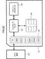
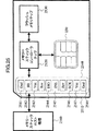
図22は、本発明を適用したMulti Media Card(Multi Media CardはInfine on TechnologiesAGの登録商標である。以下、「MMC」と略記する。)の内部構成図を簡単に表したものである。MMC110は、Multi Media Card仕様に準拠するのが好ましい。MMC110は、外部に接続したホスト機器220がMulti Media Card仕様に準拠したメモリカードコマンドを発行することによって、機密データ保護や個人認証などに必要な暗号演算をおこなうセキュリティ処理機能を持つ。ホスト機器220は、例えば、携帯電話、携帯情報端末(PDA)、パーソナルコンピュータ、音楽再生(及び録音)装置、カメラ、ビデオカメラ、自動預金預払器、街角端末、決済端末等が該当する。MMC110は、MMC外部端子140、コントローラチップ120、フラッシュメモリチップ130、ICカードチップ150を持つ。フラッシュメモリチップ130は、不揮発性の半導体メモリを記憶媒体とするメモリチップであり、フラッシュメモリコマンドによりデータの読み書きができる。MMC外部端子140は7つの端子から構成され、外部のホスト機器220と情報交換するために、電源供給端子、クロック入力端子、コマンド入出力端子、データ入出力端子、グランド端子を含む。コントローラチップ120は、MMC110内部の他の構成要素(MMC外部端子140、フラッシュメモリチップ130、ICカードチップ150)と接続されており、これらを制御するマイコンチップである。ICカードチップ150は、ICカードのプラスチック基板中に埋め込むためのマイコンチップであり、その外部端子、電気信号プロトコル、コマンドはISO/IEC7816規格に準拠している。ICカードチップ150の外部端子には、電源供給端子、クロック入力端子、リセット入力端子、I/O入出力端子、グランド端子がある。コントローラチップ120は、ICカードチップ150の外部端子からICカードチップ150にICカードコマンドを発行することによって、外部のホスト機器220から要求されたセキュリティ処理に必要な演算をおこなう。
図26は、本発明のICカードチップの内部構成を示す図である。ICカードチップ150は、演算処理を行うためのCPU(マイコン)158と、データ(プログラムを含む。)を記憶するためのROM(Read Only Memory)159とRAM(Random Access Memory)160とEEPROM(Electrically Erasable Programmable ROM)162と、暗号/復号に関する処理を行うための暗号コプロセッサ163と、外部とデータを送受信するためのシリアルインターフェース161とを備え、それらは、バス164によって接続される。そして、その暗号コプロセッサ163によって、ホスト機器220からのコマンドに応じて、ICカードチップ150自らが、セキュリティ処理を実行することが可能である。尚、暗号コプロセッサ163(ハードウェア)の替わりに、プログラム(ソフトウェア)に従ってCPU158がセキュリティ処理を実行してもよい。
一方、フラッシュメモリチップ130には、記憶素子を備えるが、マイコンは存在しない。セキュリティ処理は、例えば、ICカードチップ150内の記憶領域にデータが書き込まれるとき、又は、ICカードチップ150内の記憶領城からデータが読み出されるときに実行される。ICカードチップ150のEEPROMの記憶容量は、フラッシュメモリチップ130の記憶容量より小さい。但し、ICカードチップ150のEEPROMの記憶容量は、フラッシュメモリチップ130の記憶容量と同じでもよいし、大きくてもよい。
ICカードチップ150には、セキュリティ評価基準の国際標準であるISO/IEC15408の評価・認証機関によって認証済みである製品を利用する。一般に、セキュリティ処理をおこなう機能を持つICカードを実際の電子決済サービスなどで利用する場合、そのICカードはISO/IEC15408の評価・認証機関による評価と認定を受ける必要がある。MMCにセキュリティ処理をおこなう機能を追加することによってMMC110を実現し、それを実際の電子決済サービスなどで利用する場合、MMC110も同様にISO/IEC15408の評価・認証機関による評価と認定を受ける必要がある。本発明によれば、MMC110は、評価・認証機関によって認証済みのICカードチップ150を内蔵し、そのICカードチップ150を利用してセキュリティ処理をおこなう構造を持つことにより、セキュリティ処理機能を得る。したがって、MMC110はISO/IEC15408に基づくセキュリティ評価基準を容易に満足することができ、MMCにセキュリティ処理機能を追加するための開発期間を短縮することができる。
MMC110は、Multi Media Card仕様に準拠した外部インタフェースを持つのが好ましい。MMC110は、一種類の外部インタフェースを通じて、標準メモリカードコマンド(フラッシュメモリチップ130へアクセスするためのコマンド)に加えて、セキュリティ処理を実行するコマンドを受け付ける必要がある。コントローラチップ120は、MMC110が受信したコマンドが標準メモリカードコマンドであるか、セキュリティ処理を実行するコマンドであるかによって、アクセスすべきチップを選択し、コマンド処理を分配する機能を持つ。本発明によれば、標準メモリカードコマンドを受信したならば、フラッシュメモリチップ130を選択し、これにフラッシュメモリコマンドを発行してホストデータを読み書きできる。また、セキュリティ処理を実行するコマンドを受信したならば、ICカードチップ150を選択し、これにICカードコマンドを発行してセキュリティ処理を実行することができる。
ICカードチップ150の外部端子は、グランド端子を除いて、電源供給端子、クロック入力端子、リセット入力端子、I/O入出力端子がコントローラチップ120に接続されている。
コントローラチップ120は、電源供給端子、クロック入力端子を通して、ICカードチップ150への電源供給、クロック供給を制御する。本発明によれば、ホスト機器220からセキュリティ処理を要求されないときには、ICカードチップ150への電源供給やクロック供給を停止させることができ、MMC110の電力消費を削減することができる。
電源供給されていないICカードチップ150を、ICカードコマンドを受信できる状態にするには、まず、ICカードチップ150に電源供給を開始し、リセット処理(クロック供給の開始を含む)を施すことが必要である。例えば、コントローラチップ120は、MMC110がホスト機器220からセキュリティ処理を実行するコマンドを受信したのを契機に、電源供給端子を通してICカードチップ150への電源供給を開始してもよい。あるいは、コントローラチップ120は、セキュリティ処理を実行しないときもICカードチップ150への電源供給を維持しておき、MMC110がホスト機器220からセキュリティ処理を実行するコマンドを受信したのを契機に、リセット入力端子を通してICカードチップ150のリセット処理をおこなってもよい。本発明によれば、コントローラチップ120は、セキュリティ処理を実行するコマンドを受信するまでICカードチップ150への電源とクロック両方の供給、あるいはクロック供給のみを停止させておくことができる。したがって、MMC110の電力消費を削減することができる。ICカードチップ150がスリープモードの動作をサポートしている場合は、セキュリティ処理を実行していない時にクロック供給のみを停止するだけでも電力消費を大幅に削減できる。これはISO/IEC7816−3規格により、電源電圧3VでのICカードの電気特性は、通常動作状態で最大50mA、クロック停止状態で最大0.5mAと規定されているためである。なお、スリープモードとは、クロック供給を止めても電源さえ供給していれば、ICカードチップ150の内部状態(コアCPUのレジスタやRAMに保持されたデータ)が保存される動作モードである。
コントローラチップ120は、ICカードチップ150のクロック入力端子を通してICカードチップ150に供給するクロック信号をMMC110内部で発生し、その周波数、供給開始タイミング、供給停止タイミングを制御する機能を持つ。本発明によれば、MMC外部端子140のクロック入力端子のクロック信号と無関係にすることができるため、ホスト機器220によるタイミング解析、電力差分解析、故障利用解析と呼ばれる攻撃法に対してセキュリティが向上する。
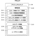
図21は、フラッシュメモリチップ130の詳細な内部構成を表している。フラッシュメモリチップ130は、ホストデータ領域2115と管理領域2110とを含む。ホストデータ領域2115は、セクタ単位に論理アドレスがマッピングされている領域であり、ホスト機器220が論理アドレスを指定してデータを読み書きできる領域である。ホストデータ領域2115は、ユーザファイル領域2130とセキュリティ処理アプリケーション領域2120とを含む。ユーザファイル領域2130は、ユーザが自由にファイルデータを読み書きできる領域である。セキュリティ処理アプリケーション領域2120は、ホスト機器220がセキュリティ処理アプリケーションに必要なデータを格納する領域であり、ユーザが不正にアクセスしないように、ホスト機器220のセキュリティ処理アプリケーションが論理的にユーザアクセス制限をかける。ここに格納するデータとしては、ホスト機器220のアプリケーションプログラム、そのアプリケーション専用のデータ、セキュリティ処理に使用される証明書など(例えば、電子決済アプリケーションプログラム、電子決済ログ情報、電子決済サービス証明書など)が可能である。本発明によれば、MMC110が、ホスト機器220がセキュリティ処理をおこなう上で使用するデータをホスト機器220の代わりに格納するため、ホスト機器220にとって利便性が向上する。一方、管理領域2110は、コントローラチップ120がICカードチップ150を管理するための情報を格納する領域である。管理領域2110は、ICカード制御パラメータ領域2111、ICカード環境設定情報領域2112、CLK2設定情報領域2113、セキュリティ処理バッファ領城2114、セキュリティ処理ステータス領域2116とを含む。2111〜2116の領域の詳細な使用法については後述する。
コントローラチップ120は、フラッシュメモリチップ130の管理領域2110のセキュリティ処理バッファ領域2114を、ICカードチップ150でセキュリティ処理を実行する際のメインメモリまたはバッファメモリとして利用する。ホスト機器220がセキュリティ処理を実行するコマンドによりMMC110にアクセスした際に、MMC110がホスト機器220からICカードチップ150に一度に送信できないほどの大きなサイズのセキュリティ関連データを受信したならば、コントローラチップ120はフラッシュメモリチップ130へのアクセスを選択し、そのデータを十分な容量を持つセキュリティ処理バッファ領域2114に一時的に格納する。ICカードチップ150に一度に送信できないほどのサイズは、ICカードコマンドの許容データサイズ(例えば、255バイト又は256バイト)を超えるサイズである。そして、コントローラチップ120はそれをICカードチップ150に送信できるサイズのデータに分割し、分割データをフラッシュメモリチップ130から読み出し、段階的にICカードチップ150に送信する。つまり、分割されたデータの読み出し、書き込みを繰り返す。本発明によれば、ホスト機器220にとって、大きなサイズのセキュリティ関連データを扱うことができるので、セキュリティ処理の利便性が向上する。
上記のセキュリティ処理バッファ領域2114を含む管理領域2110は、ホスト機器220が不正にアクセスしてセキュリティ処理を解析することができないように、コントローラチップ120により物理的にホストアクセス制限がかけられている。つまり、管理領域2110はホスト機器220が直接データを読み書きできない。本発明によれば、ホスト機器220がセキュリティ処理バッファ領域2114の内容を自由に読み出したり改ざんすることができないため、セキュリティ処理の信頼性や安全性が向上する。
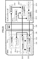
図23は、MMC110を利用したセキュリティ処理の一例として、コンテンツ配信のセキュリティ処理を表したものである。コンテンツプロバイダ2310は、MMC110を所有するユーザにコンテンツ2314を販売する業者である。ホスト機器220は、この例では、コンテンツプロバイダ2310とネットワークなどを介して接続することができる端末機である。ユーザはMMC110をホスト機器220に接続してコンテンツ2314を購入する。以下、その手順を説明する。
まず、ホスト機器220はMMC110に、フラッシュメモリチップ130に格納されたユーザ証明書2321を読み出すコマンドを発行する。MMC110のコントローラチップ120は、フラッシュメモリチップ130のセキュリティ処理アプリケーション領域2120に格納されたユーザ証明書2321を読み出し、それをホスト機器220に送信する。そして、ホスト機器220はそれをコンテンツプロバイダ2310に送信する。コンテンツプロバイダ2310はユーザ証明書2321につけられたデジタル署名を検証する(2311)。検証が成功したならば、乱数発生器によりセッション鍵を生成し(2312)、それをユーザ証明書2321から抽出したユーザ公開鍵によって暗号化する(2313)。さらに、コンテンツ2314をそのセッション鍵によって暗号化する(2315)。コンテンツプロバイダ2310はステップ2313の結果をホスト機器220に送信する。ホスト機器220は、ステップ2313の結果をユーザ秘密鍵2322によって復号するセキュリティ処理を要求するコマンドを、MMC110に発行する。コントローラチップ120は、ステップ2313の結果をユーザ秘密鍵2322によって復号するICカードコマンドを、ICカードチップ150に発行する。ICカードチップ150は、ユーザ秘密鍵2322によってステップ2313の結果を復号して、セッション鍵を取得する(2323)。ホスト機器220は、この復号処理が成功したかを示す情報を出力させるコマンドをMMC110に発行する。コントローラチップ120は、ICカードチップ150の出力する復号結果(復号処理が成功したかを示すICカードレスポンス)をもとにしてホスト機器220の求める情報を構築する。そして、MMC110はその情報をホスト機器220に送信する。次に、コンテンツプロバイダ2310は、ステップ2315の結果を、ホスト機器220に送信する。ホスト機器220は、ステップ2313の結果をセッション鍵(ステップ2323によって取得した鍵)によって復号するセキュリティ処理を要求するコマンドを、MMC110に発行する。コントローラチップ120は、ステップ2315の結果をセッション鍵によって復号するICカードコマンドを、ICカードチップ150に発行する。ICカードチップ150は、セッション鍵によってステップ2315の結果を復号して、コンテンツ2314を復元する(2324)。コントローラチップ120は、このコンテンツ2314をICカードチップ150から受信し、フラッシュメモリチップ130に書きこむ。ホスト機器220は、この復号処理が成功したかを示す情報を出力させるコマンドをMMC110に発行する。コントローラチップ120は、ICカードチップ150の出力する復号結果(復号処理が成功したかを示すICカードレスポンス)をもとにしてホスト機器220の求める情報を構築する。そして、MMC110はその情報をホスト機器220に送信する。ホスト機器220が、コンテンツを無事に受信したことをコンテンツプロバイダ2310に伝えると、コンテンツプロバイダ2310はユーザ証明書に記載されたユーザにコンテンツ料金を課金する。ユーザは、ホスト機器220でMMC110内のフラッシュメモリチップ130に格納されたコンテンツ2314を読み出して利用することができる。また、フラッシュメモリチップ130の記憶媒体に大容量のフラッシュメモリを使用すれば、多くのコンテンツを購入できる。
本発明によれば、コンテンツ配信におけるセキュリティ処理とコンテンツ蓄積の両方をMMC110によって容易に実現できる。コンテンツ料金の決済を、ICカードチップ150を利用して行ってもよい。
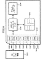
図24と図25は、それぞれ、本発明をSDカード(幅24ミリメートル、長さ32ミリメートル、厚さ2.1ミリメートルで、9つの外部端子をもち、フラッシュメモリを搭載した小型メモリカードである。)とメモリースティック(メモリースティックはソニー株式会社の登録商標である。)に適用したときの簡単な内部構成図を表したものである。本発明を適用したSDカード2410は、SDカードコントローラチップ2420、フラッシュメモリチップ2430、SDカード外部端子2440、ICカードチップ150とを含む。本発明を適用したメモリースティック2510は、メモリースティックコントローラチップ2520、フラッシュメモリチップ2530、メモリースティック外部端子2540、ICカードチップ150とを含む。フラッシュメモリチップ2430と2530は、不揮発性の半導体メモリを記憶媒体とするメモリチップであり、フラッシュメモリコマンドによりデータの読み書きができる。SDカードコントローラチップ2420とメモリースティックコントローラチップ2520はそれぞれSDカードとメモリースティック内の他の構成要素を制御するマイコンチップである。
SDカード外部端子2440は9つの端子からなり、それらの位置は、端からData2端子2441、Data3端子2442、Com端子2443、Vss端子2444、Vdd端子2445、Clock端子2446、Vss端子2447、Data0端子2448、Data1端子2449の順で並んでいる。Vdd端子2445は電源供給端子、Vss端子2444と2447はグランド端子、Data0端子2448とData1端子2449とData2端子2441とData3端子2442はデータ入出力端子、Com端子2443はコマンド入出力端子、Clock端子2446はクロック入力端子である。SDカード2410は、外部に接続するSDカードホスト機器2460とのインタフェース仕様にMMC110と違いがあるものの、MMC外部端子140と非常に類似した外部端子を持ち、MMC110と同様に外部からコマンドを発行することにより動作する特徴を持つため、本発明を適用することができる。
一方、メモリースティック外部端子2540は10個の端子からなり、それらの位置は、端からGnd端子2541、BS端子2542、Vcc端子2543、予約端子Rsvを1つ飛ばしてDIO端子2544、INS端子2545、予約端子Rsvを1つ飛ばしてSCK端子2546、Vcc端子2547、Gnd端子2548の順で並んでいる。Vcc端子2543と2547は電源供給端子、Gnd端子2541と2548はグランド端子、DIO端子2544はコマンドおよびデータ入出力端子、SCK端子2546はクロック入力端子である。メモリースティック2510は、外部に接続するメモリースティックホスト機器2560とのインタフェース仕様にMMC110と違いがあるものの、MMC110と同様に外部からコマンドを発行することにより動作する特徴を持つため、本発明を適用することができる。
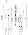
図1は、本発明を適用したMMCの詳細な内部構成図を表したものである。また、図2は、図1のMMC110と接続したホスト機器220の構成とその接続状態を表したものである。ホスト機器220は、VCC1電源221、CLK1発振器222、ホストインタフェース223を持つ。
MMC110は、外部のホスト機器220と情報交換するためのMMC外部端子140を持つ。MMC外部端子140は、CS端子141、CMD端子142、GND1端子143および146、VCC1端子144、CLK1端子145、DAT端子147の7つの端子とを含む。Multi Media Card仕様は、MMCの動作モードとしてMMCモードとSPIモードという2種類を規定しており、動作モードによってMMC外部端子140の使用法は異なる。本実施例ではMMCモードでの動作の場合について詳細に説明する。VCC1端子144は、VCC1電源221と接続されており、ホスト機器220がMMC110に電力を供給するための電源端子である。GND1端子143および146は、VCC1電源221と接続されており、MMC110の電気的なグランド端子である。GND1端子143とGND1端子146は、MMC110内部で電気的に短絡されている。CS端子141は、ホストインタフェース223に接続されており、SPIモードの動作において使用される入力端子である。ホスト機器220が、MMC110にSPIモードでアクセスするときには、CS端子141にLレベルを入力する。MMCモードの動作では、CS端子141を使用する必要はない。CMD端子142は、ホストインタフェース223に接続されており、ホスト機器220が、メモリカードインタフェース仕様に準拠したメモリカードコマンドをMMC110に送信したり、同仕様に準拠したメモリカードレスポンスをMMC110から受信するために使用する入出力端子である。DAT端子147は、ホストインタフェース223に接続されており、ホスト機器220が、メモリカードインタフェース仕様に準拠した形式の入力データをMMC110に送信したり、同仕様に準拠した形式の出力データをMMC110から受信するために使用する入出力端子である。CLK1端子145は、CLK1発振器222に接続されており、CLK1発振器222が生成するクロック信号が入力される端子である。ホスト機器220が、CMD端子142を通してメモリカードコマンド、メモリカードレスポンスを送受信したり、DAT端子147を通してホストデータを送受信するときに、CLK1端子145にクロック信号が入力される。ホストインタフェース223には、CLK1発振器222からクロック信号が供給されており、メモリカードコマンド、メモリカードレスポンス、ホストデータは、CLK1発振器222が生成するクロック信号にビット単位で同期して、ホスト機器220とMMC110との間を転送される。
MMC110は、コントローラチップ120を持つ。コントローラチップ120は、CPU121、フラッシュメモリI/F制御回路122、MMCI/F制御回路123、CLK0発振器124、VCC2生成器125、VCC2制御回路126、CLK2制御回路127、ICカードI/F制御回路128とを含む。これらの構成要素121〜128は、ホスト機器220からVCC1端子144やGND1端子143、146を通して供給された電力により動作する。MMCI/F制御回路123は、CS端子141、CMD端子142、CLK1端子145、DAT端子147と接続されており、MMC110がそれらの端子を通してホスト機器220と情報交換するためのインタフェースを制御する論理回路である。CPU121は、MMCI/F制御回路123と接続されており、MMCI/F制御回路123を制御する。MMCI/F制御回路123がCMD端子142を通してホスト機器220からメモリカードコマンドを受信すると、MMCI/F制御回路123はそのコマンドの受信が成功したかどうかの結果をホスト機器220に伝えるためCMD端子142を通してホスト機器220にレスポンスを送信する。CPU121は、受信したメモリカードコマンドを解釈し、コマンド内容に応じた処理を実行する。また、そのコマンド内容に応じてホスト機器220とDAT端子147を通してデータの送受信をおこなう必要がある場合、CPU121は、MMCI/F制御回路123へのデータの送出、MMCI/F制御回路123からのデータの取得をおこなう。さらに、CPU121は、MMCI/F制御回路123とホスト機器220との間のデータ転送手続きも制御する。例えば、ホスト機器220から受信したデータの処理中に、ホスト機器220がMMC110への電源供給を停止することがないように、CPU121はDAT端子147にLレベルを出力させ、MMC110がビジー状態であることをホスト機器220に伝える。CLK0発振器124は、CPU121と接続され、CPU121を動作させる駆動クロックを供給する。尚、ICカードチップ150は、駆動クロックを要するが、フラッシュメモリチップ130は、駆動クロックが不要である。しかし、ICカードチップ150及びフラッシュメモリチップ130は共に、データを転送するためのデータ転送クロックを要する。
MMC110は、フラッシュメモリチップ130を持つ。フラッシュメモリチップ130は、不揮発性の半導体メモリを記憶媒体とするメモリチップである。フラッシュメモリチップ130は、ホスト機器220からVCC1端子144やGND1端子143、146を通して供給された電力により動作する。フラッシュメモリチップ130は、外部からのフラッシュメモリコマンドに従って、入力されたデータを不揮発性の半導体メモリに格納するライト機能、また同メモリに格納されたデータを外部に出力するリード機能を持つ。フラッシュメモリI/F制御回路122は、フラッシュメモリチップ130にフラッシュメモリコマンドを発行したり、そのコマンドで入出力するデータを転送するための論理回路である。CPU121は、フラッシュメモリI/F制御回路122を制御し、フラッシュメモリチップ130にデータのライト機能やリード機能を実行させる。ホスト機器220から受信したデータをフラッシュメモリチップ130にライトしたり、フラッシュメモリチップ130に格納されたデータをホスト機器220に送信する必要があるとき、CPU121は、フラッシュメモリI/F制御回路122とMMCI/F制御回路123の間のデータ転送を制御する。
MMC110は、ICカードチップ150を持つ。ICカードチップ150は、ICカードの基板中に埋め込むことを目的として設計されたICチップであり、ICカードの外部端子規格に準拠した8つの外部端子を持つ。このうち6つの端子は、ICカードの外部端子規格により使用法が割り付けられており、残りの2つは将来のための予備端子である。その6つの端子は、VCC2端子151、RST端子152、CLK2端子153、GND2端子155、VPP端子156、I/O端子157である。
ICカードチップ150のグランド端子は、MMC外部端子140のGRN1(グランド端子)146に接続される。ICカードチップ150のVCC2端子(電源入力端子)151は、コントローラチップ120のVCC2制御回路126に接続される。ICカードチップ150のRST端子(リセット入力端子)152とI/O端子(データ入出力端子)157は、コントローラチップ120のICカードI/F制御回路128に接続される。ICカードチップ150のCLK2端子(クロック入力端子)153は、コントローラチップ120のCLK2制御回路127に接続される。
フラッシュメモリチップ130のVCC端子(電源入力端子)は、MMC外部端子140のVCC1144に接続される。フラッシュメモリチップ130のVSS端子(グランド端子)は、MMC外部端子140のGRD1146に接続される。フラッシュメモリチップ130のI/O端子(データ入出力端子)とレディ/ビジー端子とチップイネーブル端子とアウトプットイネーブル端子とライトイネーブル端子とクロック端子とリセット端子とは、コントローラチップ120のフラッシュメモリIF制御回路122に接続される。
VCC2端子151は、ICカードチップ150に電力を供給するための電源端子である。VCC2制御回路126は、MOS−FET素子を用いたスイッチ回路によりVCC2端子151への電力の供給開始と供給停止を制御する回路である。VCC2生成器125はVCC2端子151に供給する電圧を発生し、それをVCC2制御回路126に供給する。ICカードの電気信号規格はICカードの動作クラスとしてクラスAとクラスBを規定している。VCC2端子151に供給する標準電圧は、クラスAでは5V、クラスBでは3Vである。本発明はICカードチップ150の動作クラスによらず適用できるが、本実施例ではICカードチップ150がクラスBで動作する場合について詳細に説明する。VPP端子156は、ICカードチップ150がクラスAで動作する時に、内部の不揮発性メモリにデータを書き込んだり消去したりするために使用される可変電圧を供給する端子であり、クラスBで動作する時には使用しない。GND2端子155は、ICカードチップ150の電気的なグランド端子であり、GND1端子143、146と短絡されている。VCC2制御回路126はCPU121と接続され、CPU121はVCC2端子151への電力供給の開始と停止を制御することができる。ICカードチップ150を使用しないときは、CPU121はVCC2端子151への電力供給を停止することができる。MMC110は、ICカードチップ150への電力供給を停止することにより、それが消費する電力を節約することができる。ただし、電力供給を停止すると、ICカードチップ150の内部状態は、ICカードチップ150内部の不揮発性メモリに記憶されたデータを除いて維持されない。
CLK2端子153は、ICカードチップ150にクロック信号を入力する端子である。CLK2制御回路127は、CLK2端子153にクロックを供給する回路である。CLK2制御回路127は、CLK0発振器124から供給されたクロック信号をもとにしてCLK2端子153に供給するクロック信号を生成する。CLK2制御回路127はCPU121と接続されており、CLK2端子153へのクロックの供給開始と供給停止をCPU121から制御することができる。ICカードチップ150は、自身内部に駆動クロック発振器をもたない。そのため、CLK2端子153から駆動クロックを供給することによって動作する。CLK2制御回路127が、CLK2端子153へのクロック供給を停止すると、ICカードチップ150の動作は停止するため、ICカードチップ150の消費電力を低下させることができる。この時、VCC2端子151への電力供給が保たれていれば、ICカードチップ150の内部状態は維持される。ここで、CLK2端子153に供給するクロック信号の周波数をF2、CLK0発振器124から供給されたクロック信号の周波数をF0、PとQを正の整数とすると、CLK2制御回路127は、F2=(P/Q)*F0の関係になるようなクロック信号を作成して、これをCLK2端子153に供給する。PとQの値はCPU121により設定できるようになっている。Pを大きく設定してF2を大きくすると、ICカードチップ150の内部処理をより高速に駆動できる。Qを大きく設定してF2を小さくすると、ICカードチップ150の内部処理はより低速に駆動され、ICカードチップ150の消費電力を低下させることができる。ICカードチップ150の駆動クロック周波数は、ICカードチップ150が正しく動作できるような許容周波数範囲内に設定される必要がある。そのため、CLK2制御回路127は、F2の値がその許容周波数範囲を外れるようなPとQの値を設定させない特徴を持つ。
I/O端子157は、ICカードチップ150にICカードコマンドを入力したり、ICカードチップ150がICカードレスポンスを出力するときに使用する入出力端子である。ICカードI/F制御回路128は、I/O端子157と接続されており、I/O端子157を通してICカードコマンドの信号送信やICカードレスポンスの信号受信をおこなう回路である。ICカードI/F制御回路128はCPU121に接続されており、CPU121は、ICカードI/F制御回路128によるICカードコマンドやICカードレスポンスの送受信の手続きを制御したり、送信すべきICカードコマンドデータをICカードI/F制御回路128に設定したり、受信したICカードレスポンスをICカードI/F制御回路128から取得する。ICカードI/F制御回路128にはCLK2制御回路127からクロックが供給されており、ICカードコマンドやICカードレスポンスは、CLK2端子153に供給するクロック信号にビット単位で同期して、I/O端子157を通して送受信される。また、RST端子152は、ICカードチップ150をリセットするときにリセット信号を入力する端子である。ICカードI/F制御回路128は、RST端子152と接続されており、CPU121の指示によりICカードチップ150にリセット信号を送ることができる。
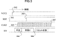
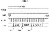
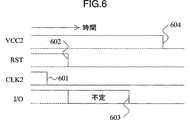
ICカードチップ150は、ICカードの電気信号規格やコマンド規格に基づいて情報交換をおこなう。ICカードチップ150へのアクセスパターンは4種類であり、図3〜図6を用いて各パターンを説明する。図3は、CPU121の指示によりICカードチップ150が非活性状態(電源が遮断されている状態)から起動して内部状態を初期化するプロセス(以下、コールドリセットと呼ぶ)において、ICカードチップ150の外部端子の信号波形をシンプルに表したものである。図4は、CPU121の指示によりICカードチップ150が活性状態(電源が供給されている状態)で内部状態を初期化するプロセス(以下、ウォームリセットと呼ぶ)において、ICカードチップ150の外部端子の信号波形をシンプルに表したものである。図5は、CPU121の指示によりICカードチップ150にICカードコマンドを送信しICカードチップ150からICカードレスポンスを受信するプロセスにおいて、ICカードチップ150の外部端子の信号波形をシンプルに表したものである。図6は、CPU121の指示によりICカードチップ150を非活性状態にするプロセスにおいて、ICカードチップ150の外部端子の信号波形をシンプルに表したものである。図3〜図6において、時間の方向は左から右にとっており、上の行から下の行に向かってVCC2端子151、RST端子152、CLK2端子153、I/O端子157で観測される信号を表す。また、破線はそれぞれの信号の基準(Lレベル)を表す。
図3を参照して、ICカードチップ150のコールドリセット操作を説明する。まず、ICカードI/F制御回路128はRST端子152をLレベルにする(301)。次に、VCC2制御回路126はVCC2端子への電源供給を開始する(302)。次に、CLK2制御回路127はCLK2端子153へのクロック信号の供給を開始する(303)。次に、ICカードI/F制御回路128はI/O端子157を状態Z(プルアップされた状態)にする(304)。次に、ICカードI/F制御回路128はRST端子152をHレベルにする(305)。次に、ICカードI/F制御回路128はI/O端子157から出力されるリセット応答の受信を開始する(306)。リセット応答の受信が終了したら、CLK2制御回路127はCLK2端子153へのクロック信号の供給を停止する(307)。これで、コールドリセットの操作が完了する。なお、ステップ307は消費電力を低下させるための工夫であり、省略してもよい。
図4を参照して、ICカードチップ150のウォームリセット操作を説明する。まず、CLK2制御回路127はCLK2端子153へのクロック信号の供給を開始する(401)。次に、ICカードI/F制御回路128はRST端子152をLレベルにする(402)。次に、ICカードI/F制御回路128はI/O端子157を状態Zにする(403)。次に、ICカードI/F制御回路128はRST端子152をHレベルにする(404)。次に、ICカードI/F制御回路128はI/O端子157から出力されるリセット応答の受信を開始する(405)。リセット応答の受信が終了したら、CLK2制御回路127はCLK2端子153へのクロック信号の供給を停止する(406)。これで、ウォームリセットの操作が完了する。なお、ステップ406は消費電力を低下させるための工夫であり、省略してもよい。
図5を参照して、ICカードチップ150にICカードコマンドを送信しICカードチップ150からICカードレスポンスを受信する操作を説明する。まず、CLK2制御回路127はCLK2端子153へのクロック信号の供給を開始する(501)。なお、クロックがすでに供給されている場合、ステップ501は不要である。次に、ICカードI/F制御回路128はI/O端子157にコマンドデータの送信を開始する(502)。コマンドデータの送信が終了したら、ICカードI/F制御回路128はI/O端子157を状態Zにする(503)。次に、ICカードI/F制御回路128はI/O端子157から出力されるレスポンスデータの受信を開始する(504)。レスポンスデータの受信が終了したら、CLK2制御回路127はCLK2端子153へのクロック信号の供給を停止する(505)。これで、ICカードコマンド送信とICカードレスポンス受信の操作が完了する。なお、ステップ505は、消費電力を低下させるための工夫であり、省略してもよい。
図6を参照して、ICカードチップ150を非活性化する操作を説明する。まず、CLK2制御回路127はCLK2端子153をLレベルにする(601)。次に、ICカードI/F制御回路128はRST端子152をLレベルにする(602)。次に、ICカードI/F制御回路128はI/O端子157をLレベルにする(603)。最後に、VCC2制御回路126はVCC2端子への電源供給を停止する(604)。これで、非活性化の操作が完了する。
尚、ICカードチップ150の停止時(例えば、セキュリティ処理を実行していない状態等)は、コントローラチップ120からICカードチップ150へ電源の供給を維持したまま、クロックの供給のみを停止してもよい。
ICカードチップ150は、機密データ保護や個人認証などに必要な暗号演算をおこなうセキュリティ処理機能を持つ。ICカードチップ150は、CPU121との間でICカードコマンドやICカードレスポンスの送受信することにより情報交換をおこない、その結果として、計算の結果や記憶されている情報の送出、記憶されている情報の変更などをおこなう。CPU121は、ICカードチップ150を利用してセキュリティ処理を実行することができる。MMC110がホスト機器220から特定のメモリカードコマンドを受信すると、CPU121はそれを契機として、VCC2制御回路126を通してICカードチップ150への電源供給を制御したり、またはCLK2制御回路127を通してICカードチップ150へのクロック供給を制御したり、またはICカードI/F制御回路128を通してICカードチップ150にICカードコマンドを送信する。これにより、CPU121は、ICカードチップ150を利用して、ホスト機器220が要求するセキュリティ処理を実行する。CPU121は、特定のメモリカードコマンドの受信を契機に、ICカードチップ150に対する電源供給制御、クロック供給制御、ICカードコマンド送信、ICカードレスポンス受信を複数組み合わせて操作することによって、セキュリティ処理を実行してもよい。また、CPU121は、ホスト機器220がMMC110へ電源供給を開始したのを契機として、セキュリティ処理を実行してもよい。セキュリティ処理の結果は、ICカードチップ150が出力するICカードレスポンスをベースにして構成され、MMC110内に保持される。MMC110がホスト機器220から特定のメモリカードコマンドを受信すると、CPU121はそれを契機として、セキュリティ処理の結果をホスト機器220に送信する。
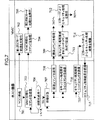
図7は、ホスト機器220がMMC110にアクセスするときのフローチャートを表したものである。まず、ホスト機器220はMMC110を活性化するためにVCC1端子144に電源供給を開始する(701)。これを契機として、MMC110は、第1次ICカード初期化処理を実行する(702)。第1次ICカード初期化処理の詳細は後述する。次に、ホスト機器220はMMC110を初期化するためにCMD端子142を通してMMC110の初期化コマンドを送信する(703)。この初期化コマンドはMulti Media Card仕様に準拠したものであり、複数種類ある。ホスト機器220は、MMC110を初期化するために、複数の初期化コマンドを送信する場合がある。MMC110が初期化コマンドを受信すると、MMC110はそれを処理する(704)。これを契機として、MMC110は、第2次ICカード初期化処理を実行する(705)。第2次ICカード初期化処理の詳細は後述する。ホスト機器220は、MMC110の初期化コマンドに対するメモリカードレスポンスを、CMD端子142を通して受信し、そのメモリカードレスポンスの内容からMMC110の初期化が完了したかを判定する。未完了ならば、再び初期化コマンドの送信をおこなう(703)。MMC110の初期化が完了したならば、ホスト機器220は、Multi Media Card仕様に準拠した標準メモリカードコマンド(フラッシュメモリチップ130へアクセスするためのコマンド)や、上に述べたセキュリティ処理に関連した特定のメモリカードコマンド(ICカードチップ150へアクセスするためのコマンド)の送信を待機する状態に移る(707)。この待機状態では、ホスト機器220は標準メモリカードコマンドを送信することができる(708)。MMC110が標準メモリカードコマンドを受信したら、MMC110はそれを処理する(709)。処理が完了したら、ホスト機器220は、再び待機状態にもどる(707)。この待機状態では、ホスト機器220はセキュリティ処理要求ライトコマンドを送信することもできる(710)。セキュリティ処理要求ライトコマンドとは、上に述べたセキュリティ処理に関連した特定のメモリカードコマンドの1種であり、MMC110にセキュリティ処理を実行させるために処理要求を送信するメモリカードコマンドである。MMC110がセキュリティ処理要求ライトコマンドを受信したら、CPU121は、要求されたセキュリティ処理の内容を解釈し、セキュリティ処理をICカードコマンドの形式で記述する(711)。即ち、CPU121は、予め定められたルールに従って、ホスト機器230からの標準メモリカードコマンドを、ICカードチップ150が解釈可能な特定のメモリカードコマンドへ変換する。そして、その結果として得られたICカードコマンドをICカードチップ150に発行するなどして、要求されたセキュリティ処理を実行する(712)。処理が完了したら、ホスト機器220は、再び待機状態にもどる(707)。この待機状態では、ホスト機器220はセキュリティ処理結果リードコマンドを送信することもできる(713)。セキュリティ処理結果リードコマンドとは、上に述べたセキュリティ処理に関連した特定のメモリカードコマンドの1種であり、MMC110によるセキュリティ処理の実行結果を知るために処理結果を受信するメモリカードコマンドである。MMC110がセキュリティ処理結果リードコマンドを受信したら、CPU121は、ICカードチップ150から受信したICカードレスポンスをベースに、ホスト機器220に送信すべきセキュリティ処理結果を構築する(714)。そして、ホスト機器220は、MMC110からセキュリティ処理結果を受信する。受信が完了したら、ホスト機器220は、再び待機状態にもどる(707)。なお、ステップ714は、ステップ712の中でおこなってもよい。
図7において、ステップ702およびステップ705で実行する第1次ICカード初期化処理および第2次ICカード初期化処理は、MMC110内でセキュリティ処理を実行するのに備えて、CPU121がICカードチップ150に対してアクセスする処理である。具体的には、ICカードチップ150の活性化や非活性化、ICカードチップ150のリセット、ICカードチップ150の環境設定を行う。環境設定とは、セキュリティ処理を実行するために必要な情報(例えば、使用可能な暗号アルゴリズムの情報、暗号計算に使用する秘密鍵や公開鍵に関する情報、個人認証に使用する認証データに関する情報など)をICカードチップ150から読み出したり、あるいはICカードチップ150に書き込んだりすることを意味する。ICカードチップ150の環境設定は、ICカードチップ150にICカードコマンドをN個(Nは正の整数)発行することによっておこなう。例えば、セッション鍵が3個必要ならば、ICカードコマンドを3回発行し、セッション鍵が2個必要ならば、ICカードコマンドを2回発行する。N個のICカードコマンドは、互いに相違するものであってもよいし、同一のものであってもよい。Nの値は固定されたものではなく、状況によってさまざまな値となる。以下、環境設定で発行するICカードコマンドを、設定コマンドと呼ぶ。また、この環境設定に基づいてセキュリティ処理を実行するICカードコマンドを、以下、セキュリティコマンドと呼ぶ。セキュリティコマンドの例としては、デジタル署名の計算、デジタル署名の検証、メッセージの暗号化、暗号化メッセージの復号、パスワードによる認証などをおこなうコマンドがある。
CPU121は、ICカードチップ150の環境設定の内容を自由に変更することができる。CPU121は、セキュリティ処理の内容や結果に応じてこれを変更してもよいし、ホスト機器からのメモリカードコマンドの受信を契機としてこれを変更してもよい。また、CPU121は、環境設定の内容を示した情報をフラッシュメモリチップ130にライトし、必要なときにフラッシュメモリチップ130からその情報をリードして使用することもできる。この情報は、図21においてICカード環境設定情報2112として示されている。これにより、MMC110が非活性化されてもその情報を保持することができ、MMC110が活性化されるたびにあらためて設定する手間を省くことができる。
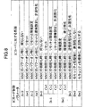
第1次ICカード初期化処理および第2次ICカード初期化処理は、ICカード制御パラメータA、B、Cに設定された値に基づいておこなわれる。また、CPU121は、ステップ712で実行するセキュリティ処理において、ICカード制御パラメータDに設定された値に基づいてICカードチップ150の活性化や非活性化を制御する。図8は、ICカード制御パラメータの種類と設定値、それに対応した処理の内容を表している。まず、パラメータAは、MMC110に電源が供給されたときに実行される第1次ICカード初期化処理に関するパラメータである。A=0のときは、CPU121はICカードチップ150にアクセスしない。A=1のときは、CPU121はICカードチップ150をコールドリセットする。A=2のときは、CPU121はICカードチップ150をコールドリセットした後でICカードチップ150の環境設定をおこなう。A=3のときは、CPU121はICカードチップ150をコールドリセットした後でICカードチップ150の環境設定をおこない、最後にICカードチップ150を非活性化する。A=0またはA=3のときは、第1次ICカード初期化処理のあとICカードチップ150が非活性状態となる。A=1またはA=2のときは、第1次ICカード初期化処理のあとICカードチップ150は活性状態となる。次に、パラメータBとCは、MMC110がMMC初期化コマンドを処理したときに実行される第2次ICカード初期化処理に関するパラメータである。B=0のときは、CPU121はICカードチップ150にアクセスしない。B=1かつC=1のときは、CPU121はICカードチップ150をリセット(コールドリセットまたはウォームリセット)する。B=1かつC=2のときは、CPU121はICカードチップ150をリセットした後でICカードチップ150の環境設定をおこなう。B=1かつC=3のときは、CPU121はICカードチップ150をリセットした後でICカードチップ150の環境設定をおこない、最後にICカードチップ150を非活性化する。B=2かつC=2のときは、CPU121はICカードチップ150の環境設定をおこなう。B=2かつC=3のときは、CPU121はICカードチップ150の環境設定をおこなった後にICカードチップ150を非活性化する。B=3のときは、ICカードチップ150が活性状態ならば、CPU121はICカードチップ150を非活性化する。最後に、パラメータDは、ホスト機器220から要求されたセキュリティ処理を実行したあとに、ICカードチップ150を非活性化するか否かを示すパラメータである。D=0のときは、セキュリティ処理の実行後に、CPU121はICカードチップ150を非活性化せず、活性状態に保つ。D=1のときは、セキュリティ処理の実行後に、CPU121はICカードチップ150を非活性化する。
CPU121は、ICカード制御パラメータA、B、C、Dの設定値を変更することができる。CPU121は、セキュリティ処理の内容や結果に応じてこれらの設定値を変更してもよいし、ホスト機器からのメモリカードコマンドの受信を契機としてこれらの設定値を変更してもよい。また、CPU121は、これらの設定値をフラッシュメモリチップ130にライトし、必要なときにフラッシュメモリチップ130からこれらの設定値をリードして使用することもできる。これらの設定値は、図21においてICカード制御パラメータ2111として示されている。これにより、MMC110が非活性化されてもこれらの設定値を保持することができ、MMC110が活性化されるたびにあらためて設定する手間を省くことができる。
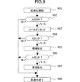
図9は、第1次ICカード初期化処理のフローチャートを表している。初期化処理を開始する(901)と、まず、ICカード制御パラメータAが0かチェックする(902)。A=0ならばそのまま初期化処理は終了する(908)。A=0でないならばICカードチップ150をコールドリセットする(903)。次に、ICカード制御パラメータAが1かチェックする(904)。A=1ならば初期化処理は終了する(908)。A=1でないならばICカードチップ150の環境設定をおこなう(905)。次に、ICカード制御パラメータAが2かチェックする(906)。A=2ならば初期化処理は終了する(908)。A=2でないならばICカードチップ150を非活性化する(907)。そして、初期化処理は終了する(908)。
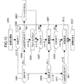
図10は、第2次ICカード初期化処理のフローチャートを表している。初期化処理を開始する(1001)と、まず、ICカード制御パラメータBが0かチェックする(1002)。B=0ならばそのまま初期化処理は終了する(1013)。B=0でないならばB=1かチェックする(1003)。B=1ならばICカード制御パラメータAが0または3かチェックする(1004)。Aが0または3ならば、ICカードチップ150をコールドリセットし(1005)、ステップ1007に移る。Aが1または2ならば、ICカードチップ150をウォームリセットし(1006)、ステップ1007に移る。ステップ1007では、ICカード制御パラメータCが1かチェックする。C=1ならば初期化処理は終了する(1013)。C=1でないならばステップ1009に移る。ステップ1003においてB=1でないならば、Bが2かチェックする(1008)。B=2ならばステップ1009に移る。B=2でないならば、ICカード制御パラメータAが0または3かチェックする(1011)。Aが0または3ならば初期化処理を終了する(1013)。Aが1または2ならば、ステップ1012に移る。ステップ1009ではICカードチップ150の環境設定をおこなう。そして、ICカード制御パラメータCが2かチェックする(1010)。C=2ならば初期化処理を終了する(1013)。C=2でないならばステップ1012に移る。ステップ1012ではICカードチップ150を非活性化する。そして、初期化処理を終了する(1013)。
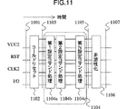
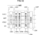
図11は、ICカードチップ150が非活性状態であるときに第1次ICカード初期化処理あるいは第2次ICカード初期化処理を実行した場合において、ICカードチップ150の外部端子の信号波形をシンプルに表したものである。図12は、ICカードチップ150が活性状態であるときに第2次ICカード初期化処理を実行した場合において、ICカードチップ150の外部端子の信号波形をシンプルに表したものである。図11と図12において、時間の方向は左から右にとっており、上の行から下の行に向かってVCC2端子151、RST端子152、CLK2端子153、I/O端子157で観測される信号を表す。また、横方向の破線はそれぞれの信号の基準(Lレベル)を表す。図11において1102は図3に示したコールドリセットの信号波形を表す。図12において1202は図4に示したウォームリセットの信号波形を表す。図11と図12において、第1設定コマンド処理1104aと1204a、第2設定コマンド処理1104bと1204b、第N設定コマンド処理1104cと1204cは、それぞれ図5に示したICカードコマンド処理の信号波形を表す。ICカードチップ150の環境設定の信号波形1104と1204は、N個の設定コマンド処理の信号波形が連なって構成される。図11と図12において、1106と1206は、それぞれ図6に示した非活性化の信号波形を表す。図11と図12において、縦方向の破線1101、1103、1105、1107、1201、1203、1205、1207はそれぞれ特定の時刻を表す。1101はコールドリセット前の時刻、1201はウォームリセット前の時刻、1103はコールドリセット後から環境設定前の間にある時刻、1203はウォームリセット後から環境設定前の間にある時刻、1105と1205は環境設定後から非活性化前の間にある時刻、1107と1207は非活性化後の時刻である。
図11を参照して、第1次ICカード初期化処理実行時の信号波形を示す。ICカード制御パラメータAが0のときは、信号波形に変化はない。A=1のときは、時刻1101から時刻1103までの範囲の信号波形となる。A=2のときは、時刻1101から時刻1105までの範囲の信号波形となる。A=3のときは、時刻1101から時刻1107までの範囲の信号波形となる。
図11を参照して、ICカード制御パラメータAが0または3のときの、第2次ICカード初期化処理実行時の信号波形を示す。ICカード制御パラメータBが0のときは、信号波形に変化はない。B=1かつICカード制御パラメータC=1のときは、時刻1101から時刻1103までの範囲の信号波形となる。B=1かつC=2のときは、時刻1101から時刻1105までの範囲の信号波形となる。B=1かつC=3のときは、時刻1101から時刻1107までの範囲の信号波形となる。
図12を参照して、ICカード制御パラメータAが1または2のときの、第2次ICカード初期化処理実行時の信号波形を示す。ICカード制御パラメータBが0のときは、信号波形に変化はない。B=1かつICカード制御パラメータC=1のときは、時刻1201から時刻1203までの範囲の信号波形となる。B=1かつC=2のときは、時刻1201から時刻1205までの範囲の信号波形となる。B=1かつC=3のときは、時刻1201から時刻1207までの範囲の信号波形となる。B=2かつC=2のときは、時刻1203から時刻1205までの範囲の信号波形となる。B=2かつC=3のときは、時刻1203から時刻1207までの範囲の信号波形となる。B=3のときは、時刻1205から時刻1207までの範囲の信号波形となる。
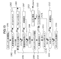
図13は、図7のステップ712において、CPU121が、ホスト機器220が要求したセキュリティ処理をICカードチップ150によって実行するときのフローチャートを表している。セキュリティ処理を開始する(1301)と、まずICカードチップ150が非活性状態かをチェックする(1302)。非活性状態ならば、ICカードチップ150をコールドリセットし(1303)、ステップ1306に移る。活性状態ならば、ステップ1304に移る。ステップ1304では、ICカードチップ150にICカードコマンドを発行する前にICカードチップ150を再リセットする必要があるかをチェックする。必要があるならば、ICカードチップ150をウォームリセットし(1305)、ステップ1306に移る。必要がないならば、ステップ1306に移る。ステップ1306では、ICカードチップ150の環境設定をおこなう必要があるかをチェックする。必要があるならば、ICカードチップ150の環境設定をおこない(1307)、ステップ1308に移る。必要がないならば、ステップ1308に移る。ステップ1308では、ICカードチップ150のCLK2端子に供給するクロック信号の周波数F2を設定する。そして、CPU121はICカードチップ150にセキュリティコマンドを発行し、ICカードチップ150はそれを処理する(1309)。セキュリティコマンドの処理時間は、クロック周波数F2に依存する。次に、ICカードチップ150が出力するICカードレスポンスにより、その処理が成功したかどうかを判定する(1310)。成功ならば、ステップ1311に移る。失敗ならば、ステップ1312に移る。ステップ1311では、ICカードチップ150に発行すべきセキュリティコマンドが全て完了したかをチェックする。発行すべきセキュリティコマンドがまだあるならば、ステップ1304に移る。発行すべきセキュリティコマンドが全て完了したならば、ステップ1314に移る。ステップ1312では、失敗したセキュリティコマンドをリトライすることが可能かを判定する。リトライできるなら、リトライ設定をおこない(1313)、ステップ1304に移る。リトライ設定とは、リトライすべきセキュリティコマンドやその関連データをCPU121が再度準備することである。リトライできないならステップ1314に移る。これは、ホスト機器220が要求したセキュリティ処理が失敗したことを意味する。ステップ1314では、ICカード制御パラメータDをチェックする。D=1ならば、ICカードチップ150を非活性化して(1315)、セキュリティ処理を終了する(1316)。D=1でないならば、ICカードチップ150を活性状態に保ったままセキュリティ処理を終了する(1316)。図13のフローチャートにおいては、クロック周波数F2を、ステップ1309で発行するセキュリティコマンドの種類によって変えることができるように、ステップ1308をステップ1309の直前に位置させたが、ステップ1308はそれ以外の位置にあってもよい。
従来のICカードへの攻撃法を有効にしている要因のひとつとして、ICカードの駆動クロックが外部の接続装置から直接供給されることがあげられる。駆動クロックが接続装置の制御下にあるため、タイミング解析や電力差分解析においては、電気信号の測定においてICカード内部処理のタイミングの獲得が容易になる。一方、故障利用解析においては、異常な駆動クロックの供給による演算エラーの発生が容易になる。これに対し、本発明によれば、MMC110内部でICカードチップ150によりセキュリティ処理を実行するとき、ホスト機器220はICカードチップ150の駆動クロックを直接供給できない。CPU121は、ICカードチップ150へ供給するクロックの周波数F2を自由に設定することができる。これにより、ホスト機器220の要求する処理性能に柔軟に対応したセキュリティ処理が実現できる。ホスト機器220が高速なセキュリティ処理を要求するならば周波数F2を高く設定し、低い消費電力を要求するならば周波数F2を低く設定したり、クロックを適度に停止させればよい。また、CPU121は、周波数F2だけでなくクロックの供給開始タイミング、供給停止タイミングを自由に設定できる。これらをランダムに変化させることにより、ICカードチップ150に対するタイミング解析、電力差分解析、故障利用解析と呼ばれる攻撃法を困難にすることができる。タイミング解析は、攻撃者が暗号処理1回の処理時間を正確に計測可能であることを仮定しているため、その対策としては、攻撃者が処理時間計測を正確に行えないようにすることが有効である。本発明によりタイミング解析が困難になる理由は、ICカードチップ150がICカードコマンドを処理している時間の長さをホスト機器220が正確に計測できないためである。電力差分解析の対策としては、処理の実行タイミングや順序に関する情報を外部から検出不可能にすることが有効である。本発明により電力差分解析が困難になる理由は、ICカードコマンドが発行された時刻、発行されたICカードコマンドの内容、発行されたICカードコマンドの順序(ICカードコマンドを複数組み合わせてセキュリティ処理を実行する場合)の検出がホスト機器220にとって困難になるためである。故障利用解析の対策としては、ICカードにクロックや電圧や温度等の動作環境検知回路を搭載し、異常を検出したならば処理を停止あるいは使用不能にするという方法が有効である。本発明により故障利用解析が困難になる理由は、CLK2制御回路127がICカードチップ150に異常な駆動クロックを供給しないことが、ホスト機器220がICカードチップ150に演算エラーを発生させるのを防止するからである。
CPU121は、ICカードチップ150に供給するクロックの周波数F2、供給開始タイミング、供給停止タイミングの設定値を、セキュリティ処理の内容や結果に応じて変更してもよいし、ホスト機器からのメモリカードコマンドの受信を契機として変更してもよい。また、CPU121は、これらの設定値をフラッシュメモリチップ130にライトし、必要なときにフラッシュメモリチップ130からこれらの設定値をリードして使用することもできる。これらの設定値は、図21においてCLK2設定情報2113として示されている。これにより、MMC110が非活性化されてもこれらの設定値を保持することができ、MMC110が活性化されるたびにあらためて設定する手間を省くことができる。
図14は、ホスト機器220がセキュリティ処理要求ライトコマンドをMMC110に発行してから、ICカードチップ150でセキュリティ処理が実行されるまでの過程(図7のステップ710〜712)において、MMC110およびICカードチップ150の外部端子の信号波形、CPU121によるフラッシュメモリチップ130へのアクセスをシンプルに表したものである。図14において、時間の方向は左から右にとる。一番上の行はフラッシュメモリチップ130へのアクセス内容である。上から二行目の行から下の行に向かって、VCC1端子144、CMD端子142、CLK1端子145、DAT端子147、VCC2端子151、RST端子152、CLK2端子153、I/O端子157で観測される信号を表す。また、横方向の破線はそれぞれの信号の基準(Lレベル)を表す。図14を参照して、ホスト機器220がセキュリティ処理要求ライトコマンドをMMC110に発行してから、ICカードチップ150でセキュリティ処理が実行されるまでの過程を説明する。まず、ホスト機器220はCMD端子142にセキュリティ処理要求ライトコマンドを送信する(1401)。次に、ホスト機器220はCMD端子142からセキュリティ処理要求ライトコマンドのレスポンスを受信する(1402)。このレスポンスは、MMC110がコマンドを受信したことをホスト機器220に伝えるものであり、セキュリティ処理の実行結果ではない。次に、ホスト機器220はDAT端子147にセキュリティ処理要求を送信する(1403)。セキュリティ処理要求とは、セキュリティ処理の内容や処理すべきデータを含むホストデータである。次に、MMC110はDAT端子147をLレベルにセットする(1404)。MMC110は、これによりビジー状態であることをホスト機器220に示す。次に、CPU121は、ホスト機器220から受信したセキュリティ処理要求をフラッシュメモリチップ130にライトするコマンドを発行する(1405)。セキュリティ処理要求をフラッシュメモリチップ130にライトすることにより、CPU121がセキュリティ処理要求をICカードコマンド形式で記述する処理(図7のステップ711)において、CPU121内部のワークメモリの消費量を節約できる。これは、セキュリティ処理要求のデータサイズが大きいときに有効である。なお、フラッシュメモリチップ130にライトされたセキュリティ処理要求は、図21においてセキュリティ処理バッファ領域2114に格納される。また、ライトコマンド発行1405は必須な操作ではない。ライト処理期間1406は、フラッシュメモリチップ130がセキュリティ処理要求のライト処理を実行している期間を表す。セキュリティ処理1407はICカードチップ150によるセキュリティ処理の信号波形を表す。この信号波形は図13のフローチャートの遷移過程に依存する。セキュリティ処理1407は、ライト処理期間1406とオーバラップさせることができる。一般にフラッシュメモリチップ130のライト処理期間1406はミリ秒のオーダーであるため、セキュリティ処理1407とオーバラップさせることは、セキュリティ処理の全体的な処理時間の短縮にとって有効である。リード/ライト1408は、セキュリティ処理1407の実行中に、フラッシュメモリチップ130からセキュリティ処理要求をリードしたり、ICカードチップ150が出力した計算結果をフラッシュメモリチップ130にライトするアクセスを示している。このアクセスにより、CPU121内部のワークメモリの消費量を節約できる。これは、セキュリティ処理要求やセキュリティ処理結果のデータサイズが大きいときに有効である。リード/ライト1408は必須ではない。セキュリティ処理1407が完了したら、MMC110はDAT端子147をHレベルにセットする(1409)。MMC110は、これによりセキュリティ処理が完了したことをホスト機器220に示す。
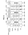
図15は、図14におけるセキュリティ処理1407の信号波形の一例を表したものである。図15において、時間の方向は左から右にとる。一番上の行はフラッシュメモリチップ130へのアクセス内容である。上から二行目の行から下の行に向かって、VCC2端子151、RST端子152、CLK2端子153、I/O端子157で観測される信号を表す。また、横方向の破線はそれぞれの信号の基準(Lレベル)を表す。1501は図3に示したコールドリセットの信号波形を表し、1504は図4に示したウォームリセットの信号波形を表し、1502および1505は図11(あるいは図12)に示した環境設定の信号波形を表し、1503および1506および1507は図5に示したICカードコマンド処理の信号波形を表し、1508は図6に示した非活性化の信号波形を表す。ICカードチップ150の外部端子において図15に示した信号波形が観測されるのは、図13のフローチャートが1301、1302、1303、1306、1307、1308、1309、1310、1311、1304、1305、1306、1307、1308、1309、1310、1311、1304、1306、1308、1309、1310、1311、1314、1315、1316の順で遷移するときである。図15を参照して、図14のセキュリティ処理1407の実行中におけるCPU121によるフラッシュメモリチップ130へのアクセス(リード/ライト1408)を説明する。このアクセスには、図21におけるセキュリティ処理バッファ領域2114を使用する。リード1509、1511、1512は、それぞれ、セキュリティコマンド処理1503、1506、1507においてICカードチップ150に送信するICカードコマンドを構築するために必要なデータを、フラッシュメモリチップ130からリードするアクセスである。ライト1510は、セキュリティコマンド処理1503においてICカードチップ150が出力した計算結果を、フラッシュメモリチップ130にライトするアクセスである。ライト1513は、セキュリティコマンド処理1506および1507においてICカードチップ150が出力した計算結果を、フラッシュメモリチップ130にまとめてライトするアクセスである。リード1509、1511、1512は、それぞれ、セキュリティコマンド処理1503、1506、1507以前のICカードチップ150へのアクセスとオーバラップさせることができる。ライト1510、1513は、それぞれ、セキュリティコマンド処理1503、1507以後のICカードチップ150へのアクセスとオーバラップさせることができる。これらのオーバラップは、セキュリティ処理の全体的な処理時間の短縮にとって有効である。さらに、フラッシュメモリチップ130のライト単位が大きい場合は、ライト1513のように複数の計算結果をまとめてライトすることができる。これは、フラッシュメモリチップ130へのライト回数を削減し、フラッシュメモリチップ130の劣化を遅らせる効果がある。なお、ライト1510、1513でフラッシュメモリチップ130にライトする内容は、ICカードチップ150が出力した計算結果そのものに限定されず、図7のステップ715でホスト機器220に返すセキュリティ処理結果またはその一部であってもよい。この場合、図7のステップ714またはその一部は、ステップ712の中で実行されることになる。
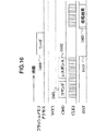
図16は、ホスト機器220がセキュリティ処理結果リードコマンドをMMC110に発行してから、MMC110がセキュリティ処理結果を出力するまでの過程(図7のステップ713〜715)において、MMC110の外部端子の信号波形、CPU121によるフラッシュメモリチップ130へのアクセスをシンプルに表したものである。図16において、時間の方向は左から右にとる。一番上の行はフラッシュメモリチップ130へのアクセス内容である。上から二行目の行から下の行に向かって、VCC1端子144、CMD端子142、CLK1端子145、DAT端子147で観測される信号を表す。また、横方向の破線はそれぞれの信号の基準(Lレベル)を表す。図16を参照して、ホスト機器220がセキュリティ処理結果リードコマンドをMMC110に発行してから、MMC110がセキュリティ処理結果を出力するまでの過程を説明する。まず、ホスト機器220はCMD端子142にセキュリティ処理結果リードコマンドを送信する(1601)。次に、ホスト機器220はCMD端子142からセキュリティ処理結果リードコマンドのレスポンスを受信する(1602)。このレスポンスは、MMC110がコマンドを受信したことをホスト機器220に伝えるものであり、セキュリティ処理結果ではない。次に、MMC110はDAT端子147をLレベルにセットする(1603)。MMC110は、これによりビジー状態であることをホスト機器220に示す。次に、CPU121は、フラッシュメモリチップ130のセキュリティ処理バッファ領域(図21の2114)から、ICカードチップ150が出力した計算結果をリードする(1604)。CPU121は、これをもとにセキュリティ処理結果を構築し、MMC110がDAT端子147にセキュリティ処理結果を出力する(1605)。なお、図7のステップ714またはその一部が、ステップ712の中で実行されている場合、ステップ1604ではフラッシュメモリチップ130のセキュリティ処理バッファ領域(図21の2114)からセキュリティ処理結果またはその一部をリードする。なお、フラッシュメモリチップ130のセキュリティ処理バッファ領域(図21の2114)を利用しないでセキュリティ処理結果を構築する場合、ステップ1604は必要ない。
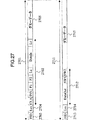
図27は、図7のステップ710においてMMC110に送信するセキュリティ処理要求データ、およびステップ715でホスト機器220が受信するセキュリティ処理結果データそれぞれのフォーマットの一例を示したものである。このフォーマットは、要求されたセキュリティ処理の内容が1つのICカードコマンドで表現でき、セキュリティ処理の結果が1つのICカードレスポンスで表現できる場合に適用することが好ましい。ICカードチップ150に送信するICカードコマンド、ICカードチップ150から受信するICカードレスポンスはともにISO/IEC7816−4規格に従う。本規格によれば、ICカードコマンドの構成は、4バイトのヘッダ(クラスバイトCLA、命令バイトINS、パラメータバイトP1とP2)が必須であり、必要に応じて、入力データ長指示バイトLc、入力データData In、出力データ長指示バイトLeが後に続く。また、ICカードレスポンスの構成は、2バイトのステータスSW1とSW2が必須であり、必要に応じて、出力データData Outがその前に置かれる。本フォーマットにおけるセキュリティ処理要求のデータ2701は、ICカードコマンド2702の前にフォーマット識別子FID2703とICカードコマンド長Lca2704を付け、さらにICカードコマンド2702の後にダミーデータ2705をパディングしたものである。FID2703はフォーマットの識別番号またはフォーマットの属性データを含む。Lca2704の値はICカードコマンド2702の各構成要素の長さを合計した値である。一方、セキュリティ処理結果のデータ2711は、ICカードレスポンス2712の前にフォーマット識別子FID2713とICカードレスポンス長Lra2714を付け、さらにICカードレスポンス2712の後にダミーデータ2715をパディングしたものである。FID2713はフォーマットの識別番号またはフォーマットの属性データを含む。Lra2714の値はICカードレスポンス2712の各構成要素の長さを合計した値である。なお、この図では、ICカードコマンドにLc、Data In、Leが含まれ、ICカードレスポンスにData Outが含まれる場合のフォーマット例を表している。Multi Media Card仕様では、リード/ライトアクセスするデータを固定長のブロック単位で処理することが標準となっている。よって、セキュリティ処理要求のデータ2701やセキュリティ処理結果のデータ2711のサイズもMulti Media Card仕様に準拠したブロックサイズに一致させることが好ましい。ダミーデータ2705、2715は、セキュリティ処理要求のデータ2701やセキュリティ処理結果のデータ2711のサイズをブロックサイズに一致させるために適用される。ブロックサイズとして採用する値は、一般の小型メモリカードが論理ファイルシステムに採用しているFAT方式におけるセクタサイズ(512バイト)が望ましい。パディングするダミーデータ2705、2715は全てゼロでもよいし、乱数でもよいし、CPU121やホスト機器220がデータエラーを検出したり訂正するためのチェックサムでもよい。Lca2704の値はCPU121がセキュリティ処理要求のデータ2701からダミーデータ2705を除去するために使用し、Lra2714の値はホスト機器220がセキュリティ処理結果のデータ2711からダミーデータ2715を除去するために使用する。
MMC110の製造者や管理者は、セキュリティシステムのユーザにMMC110を提供する前やそのユーザが所有するMMC110に問題が発生した時に、MMC110に内蔵されたICカードチップ150に様々な初期データを書きこんだり、ICカードチップ150のテストをおこなったりする必要がある。MMC110の製造者や管理者によるこれらの操作の利便性を高めるために、MMC110は、ICカードチップ150の外部端子をMMC外部端子140に割りつけるインタフェース機能を持つ。これにより、図3〜図6で示したようなICカードチップ150へのアクセス信号を、MMC外部端子140から直接送受信できる。このようなMMC110の動作モードを、Multi Media Card仕様に準拠した動作モードと区別して、以下、インタフェース直通モードと呼ぶ。
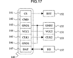
インタフェース直通モードについて詳細に説明する。図17は、ICカードチップ150の外部端子をMMC外部端子140に割りつけるときの対応関係の一例を表している。この例では、RST端子152をCS端子141に割り付け、GND2端子155をGND1端子143、146に割り付け、VCC2端子151をVCC1端子144に割り付け、CLK2端子153をCLK1端子145に割り付け、I/O端子157をDAT端子147に割り付ける。このとき、CS端子141とCLK1端子145は入力端子、DAT端子147は入出力端子として機能する。
MMC110は、特定のメモリカードコマンドを受信すると、動作モードをインタフェース直通モードへ移したり、インタフェース直通モードからMulti Media Card仕様に準拠した動作モードに戻すことができる。以下、動作モードをインタフェース直通モードへ移すメモリカードコマンドを直通化コマンド、動作モードをインタフェース直通モードから通常の状態に戻すメモリカードコマンドを復帰コマンドと呼ぶ。図1を参照して、MMCI/F制御回路123は、VCC2制御回路126、CLK2制御回路127、ICカードI/F制御回路128と接続されており、MMC110がホスト機器220から直通化コマンドを受信すると、CPU121の指示により図17で示した端子割り付けをおこなう。MMC110がホスト機器220から復帰コマンドを受信すると、CPU121の指示により図17で示した端子割り付けを解除し、MMC110はMulti Media Card仕様に準拠した動作モードに戻る。
インタフェース直通モードでは、ホスト機器220がICカードチップ150に直接アクセスできるため、セキュリティの観点からインタフェース直通モードを利用できるのは限られた者だけにする必要がある。そこで、直通化コマンドの発行には、一般のユーザに知られないパスワードの送信を必要とする。正しいパスワードが入力されないとインタフェース直通モードは利用できない。
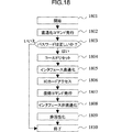
図18は、ホスト機器220が、MMC110の動作モードをMulti Media Card仕様に準拠した動作モードからインタフェース直通モードに移し、ICカードチップ150に直接アクセスし、その後、MMC110の動作モードを再びMulti Media Card仕様に準拠した動作モードに戻すまでの処理のフローチャートを表している。ホスト機器220は処理を開始し(1801)、まずMMC110に直通化コマンドを発行する(1802)。MMC110は、直通化コマンドで送信されたパスワードが正しいかチェックする(1803)。正しければステップ1804に移り、間違っていれば処理は終了する(1810)。ステップ1804では、CPU121は、ICカードチップ150をコールドリセットする。そして、図17で示した端子割り付けをおこないインタフェースを直通化する(1805)。この時点から、ホスト機器220はICカードチップ150に直接アクセスする(1806)。ホスト機器220がICカードチップ150への直接アクセスを終了し、MMC110の動作モードを再びMulti Media Card仕様に準拠した動作モードに戻すときは、MMC110に復帰コマンドを発行する(1807)。すると、CPU121は図17で示した端子割り付けを解除し、MMC110はMulti Media Card仕様に準拠した動作モードに戻る(1808)。そして、CPU121は、ICカードチップ150を非活性化する(1809)。以上で、処理は終了する(1810)。
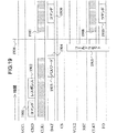
図19は、図18のステップ1801〜1806の過程において、MMC110およびICカードチップ150の外部端子の信号波形をシンプルに表したものである。図19において、時間の方向は左から右にとる。上の行から下の行に向かって、VCC1端子144、CMD端子142、CLK1端子145、DAT端子147、VCC2端子151、RST端子152、CLK2端子153、I/O端子157で観測される信号を表す。また、横方向の破線はそれぞれの信号の基準(Lレベル)を表す。1905は、図3のコールドリセットの信号波形を示す。モード移行時刻1906は、動作モードがインタフェース直通モードに移る時刻を表す。
図19を参照して、ホスト機器220がMMC110の動作モードをMulti Media Card仕様に準拠した動作モードからインタフェース直通モードに移しICカードチップ150に直接アクセスする過程を説明する。なお、MMC110のVCC1端子144には3V(VCC2端子151の標準電圧)が供給されている。ホスト機器220がCMD端子142に直通化コマンドを入力すると(1901)、CMD端子142から直通化コマンドのレスポンスが出力される(1902)。このレスポンスは、MMC110がコマンドを受信したことをホスト機器220に伝えるものである。次に、ホスト機器220はDAT端子147にパスワードを入力する(1903)。パスワード入力後、MMC110はDAT端子147にLレベルを出力し(1904)、ビジー状態であることをホスト機器220に示す。ビジー状態の間に、CPU121は、ICカードチップ150をコールドリセットする(1905)。そして、モード移行時刻1906において、動作モードをインタフェース直通モードに移す。このときに、DAT端子147はLレベルからハイインピーダンス状態になる。これにより、ホスト機器220はビジー状態の解除を知ることができる。この時点から、ホスト機器220はICカードチップ150に直接アクセスする。例えば、CLK1端子145にクロックを供給すると(1907)、CLK2端子153にそのクロックが供給される(1908)。また、DAT端子147にICカードコマンドを送信すると(1909)、I/O端子157にそのICカードコマンドが送信される(1910)。
図20は、図18のステップ1807〜1810の過程において、MMC110およびICカードチップ150の外部端子の信号波形をシンプルに表したものである。図20において、時間の方向は左から右にとる。上の行から下の行に向かって、VCC1端子144、CMD端子142、CLK1端子145、DAT端子147、VCC2端子151、RST端子152、CLK2端子153、I/O端子157で観測される信号を表す。また、横方向の破線はそれぞれの信号の基準(Lレベル)を表す。モード復帰時刻2003は、動作モードがインタフェース直通モードからMulti Media Card仕様に準拠した動作モードに戻る時刻を表す。2004は、図6の非活性化の信号波形を示す。
図20を参照して、ホスト機器220がMMC110の動作モードをインタフェース直通モードからMulti Media Card仕様に準拠した動作モードに戻す過程を説明する。なお、MMC110のVCC1端子144には3V(VCC2端子151の標準電圧)が供給されている。ホスト機器220がCMD端子142に復帰コマンドを入力すると(2001)、CMD端子142から復帰コマンドのレスポンスが出力される(2002)。このレスポンスは、MMC110がコマンドを受信したことをホスト機器220に伝えるものである。そして、モード復帰時刻2003において、MMC110はDAT端子147にLレベルを出力してビジー状態であることをホスト機器220に示し、それと同時に動作モードをMulti Media Card仕様に準拠した動作モードに戻す。ビジー状態の間に、CPU121は、ICカードチップ150を非活性化する(2004)。そして、MMC110は、DAT端子147をハイインピーダンス状態にし(2005)、復帰コマンドの処理が完了したことをホスト機器220に示す。これ以後、ホスト機器220はICカードチップ150に直接アクセスできない。ホスト機器220が、CLK1端子145にクロックを供給しながらCMD端子142に何らかのメモリカードコマンドを送信した場合、ICカードチップ150にそのクロック信号(2006)は伝わらない。2001や2002においてホスト機器220がCLK1端子145に供給するクロック信号は、ICカードチップ150のCLK2端子153にも伝わるが、DAT端子147がハイインピーダンス状態であるため、ICカードチップ150がICカードコマンドを誤って認識することはない。
図21において、セキュリティ処理ステータス領域2116には、ICカードチップ150によるセキュリティ処理の進捗状況を示す情報を格納する。CPU121は、この情報をセキュリティ処理の実行中に更新することができる。例えば、セキュリティ処理の途中でMMC110への電源供給が停止した場合、電源供給再開時にCPU121がこの情報をリードして参照すれば、セキュリティ処理を中断した段階から再開することができる。
本発明の実施形態によれば、メモリカード外部からICチップの駆動クロックを直接供給しないため、ICチップの処理時間を正確に計測できず、また、処理の実行タイミングや順序の検出が困難になる。さらに、異常な駆動クロックを供給することができず、演算エラーを発生させるのが困難になる。したがって、タイミング解析、電力差分解析、故障利用解析攻撃法に対するセキュリティが向上する。
本発明の実施形態によれば、メモリカード外部からICチップの制御方式を自由に設定できる。例えば、高速処理が要求されるならば、ICチップの駆動クロックの周波数を高くした制御方式を設定し、低消費電力が要求されるならば、ICチップの駆動クロックの周波数を低くしたり、ICチップの駆動クロックを適度に停止させる制御方式を設定することができる。したがって、セキュリティシステムの要求する処理性能に柔軟に対応したセキュリティ処理が実現できる。
本発明によれば、ICチップによるセキュリティ処理に必要なデータや、ICチップを管理するための情報を、フラッシュメモリに保持することができる。したがって、セキュリティ処理の利便性を向上させることができる。
本発明の実施形態によれば、MMCの製造者や管理者が、MMC内部のICチップに直接アクセスすることができる。したがって、MMC内部のICチップの初期化やメンテナンスを、従来のICカードと同様な方法で実現できる。
本発明の実施形態によれば、フラッシュメモリチップを備えたMMCに、セキュリティ機能を追加する場合、セキュリティ評価機関の認証を予め受けたICカードチップ追加搭載することによって、セキュリティ評価機関によるMMCの認証が不要となるため、MMCの開発期間又は製造期間が短縮する。
産業上の利用可能性
本発明によれば、記憶装置のセキュリティを向上するという効果を奏する。
本発明によれば、記憶装置の製造が簡略化されるという効果を奏する。
上記記載は実施例についてなされたが、本発明はその精神と添付クレームの範囲内で種々の変更および修正をすることができることは当業者に明らかである。
【図面の簡単な説明】
第1図は、本発明を適用したMMCの内部構成を示す図である。
第2図は、本発明を適用したMMCのホスト機器の内部構成、およびホスト機器とMMCとの接続状態を示す図である。
第3図は、ICカードチップのコールドリセット時の信号波形を示す図である。
第4図は、ICカードチップのウォームリセット時の信号波形を示す図である。
第5図は、ICカードチップのICカードコマンド処理時の信号波形を示す図である。
第6図は、ICカードチップの非活性化時の信号波形を示す図である。
第7図は、ホスト機器によるMMCへのアクセスを示したフローチャートである。
第8図は、ICカード制御パラメータとそれに対応するICカードへの処理内容を示す図表である。
第9図は、ICカードチップに対する第1次ICカード初期化の詳細なフローチャートである。
第10図は、ICカードチップに対する第2次ICカード初期化の詳細なフローチャートである。
第11図は、非活性状態のICカードチップに対するICカード初期化時の信号波形を示す図である。
第12図は、活性状態のICカードチップに対するICカード初期化時の信号波形を示す図である。
第13図は、ICカードチップによるセキュリティ処理の詳細なフローチャートである。
第14図は、セキュリティ処理要求ライトコマンドを処理するときの信号波形とフラッシュメモリチップアクセスを示す図である。
第15図は、ICカードチップによるセキュリティ処理実行時の信号波形とフラッシュメモリチップアクセスの一例を示す図である。
第16図は、セキュリティ処理結果リードコマンドを処理するときの信号波形とフラッシュメモリチップアクセスを示す図である。
第17図は、インタフェース直通モードにおけるMMC外部端子とICカードチップ外部端子の対応関係を示す図である。
第18図は、インタフェース直通モードへ移行する処理とインタフェース直通モードから復帰する処理のフローチャートである。
第19図は、インタフェース直通モードへ移行する処理時の信号波形を示す図である。
第20図は、インタフェース直通モードから復帰する処理時の信号波形を示す図である。
第21図は、フラッシュメモリチップの内部構成を示す図である。
第22図は、本発明を適用したMMCの内部構成を簡単に示す図である。
第23図は、本発明を適用したMMCをコンテンツ配信に応用した例を示す図である。
第24図は、本発明を適用したSDカードの内部構成を簡単に示す図である。
第25図は、本発明を適用したメモリースティックの内部構成を簡単に示す図である。
第26図は、本発明のICカードチップの内部構成を示す図である。
第27図は、セキュリティ処理要求とセキュリティ処理結果の各データフォーマットの一例を示す図である。Technical field
The present invention relates to a storage device having a security function, a host device into which the storage device can be inserted, and a host device into which the storage device is inserted, and more particularly to an electrically erasable nonvolatile memory (for example, a flash memory). ), A host device into which the memory card can be inserted, and a host device into which the memory card is inserted.
Background art
An IC card is obtained by embedding an IC (integrated circuit) chip in a plastic card substrate, and has an external terminal of the IC chip on its surface. The external terminals of the IC chip include a power supply terminal, a clock terminal, and a data input / output terminal. The IC chip operates when the connecting device directly supplies power and a driving clock from an external terminal. The IC card exchanges information with the connection device by transmitting and receiving electrical signals to and from the connection device such as a terminal through an external terminal. As a result of the information exchange, the IC card sends out calculation results, stored information, and changes stored information. The IC card can have a function of executing security processing such as protection of confidential data and personal authentication based on these operation specifications. IC cards are used as user devices for personal identification in systems that require security of confidential information such as credit card payments and banking.
The IC card used in the security system needs to be designed so that the secret information or information that can be used to estimate the secret information is not exposed when performing calculations using the secret information. That is, it is required to have tamper resistance. As an attack method for analyzing secret information that should not be given outside, timing analysis, power difference analysis, failure utilization analysis, and the like are known.
Timing analysis is an attack method that estimates secret information by statistically analyzing the time difference when the cryptographic processing time differs depending on the content of the secret information. When implementing cryptographic algorithms, optimization may be applied such as skipping unnecessary processing or performing branch processing depending on the content of confidential information for the purpose of reducing processing time and program size. . When such optimization is applied, the encryption processing time varies depending on the content of the secret information. Therefore, there is a possibility that the content of the secret information can be estimated by looking at the processing time.
The power difference analysis is an attack method that estimates the secret information by measuring the power supplied from the power supply terminal of the IC card during the execution of the cryptographic process and analyzing the difference in power consumption therefrom.
The failure use analysis is an attack method using a calculation error of the IC card. The IC card is given a temporary failure or a limited failure that does not affect other functions, and the IC card is caused to perform an abnormal process desired by the attacker. When an error is intentionally generated by applying a high voltage to the IC card or by instantaneously changing the clock frequency or drive voltage, confidential information can be obtained from the incorrect calculation result and the correct calculation result. There is sex.
IC cards must have countermeasures against these attack methods in practice.
Disclosure of the invention
A first object of the present invention is to provide a storage device with improved security.
A second object of the present invention is to provide a storage device that is simplified in manufacture.
In order to achieve the first object, the present invention is based on a memory capable of storing data, a processing device capable of storing data and capable of executing data security processing, and a command from an external host device. And a controller for controlling the memory and the processing device.
In order to achieve the first object, the present invention comprises a flash memory chip, a controller, an external terminal, and an IC chip, the ground terminal of the IC chip is connected to the external terminal, and the power input terminal of the IC chip The reset input terminal, the clock input terminal, and the data input / output terminal are connected to the controller.
In order to achieve the second object, a flash memory chip capable of storing data, a controller for controlling reading / writing of data to / from the flash memory chip, and an IC chip are provided, and the IC chip is pre-authenticated by an authentication authority. It will be installed after.
Other objects, features and advantages of the present invention will become apparent from the following description of embodiments of the present invention with reference to the accompanying drawings.
BEST MODE FOR CARRYING OUT THE INVENTION
Hereinafter, an embodiment of the present invention will be described.
FIG. 22 simply shows an internal configuration diagram of Multi Media Card to which the present invention is applied (Multi Media Card is a registered trademark of Infine on Technologies AG. Hereinafter, abbreviated as “MMC”). The MMC 110 preferably conforms to the Multi Media Card specification. The MMC 110 has a security processing function for performing cryptographic operations necessary for confidential data protection, personal authentication, and the like when the
FIG. 26 is a diagram showing the internal configuration of the IC card chip of the present invention. The
On the other hand, the
For the
The MMC 110 preferably has an external interface compliant with the Multi Media Card specification. The MMC 110 needs to accept a command for executing a security process in addition to a standard memory card command (a command for accessing the flash memory chip 130) through one type of external interface. The
With respect to the external terminals of the
The
In order to make the
The
FIG. 21 shows a detailed internal configuration of the
The
The
FIG. 23 shows content distribution security processing as an example of security processing using the
First, the
According to the present invention, both security processing and content accumulation in content distribution can be easily realized by the
FIG. 24 and FIG. 25 show a small memory card according to the present invention, which is an SD card (width 24 mm, length 32 mm, thickness 2.1 mm, has nine external terminals, and is equipped with a flash memory. ) And Memory Stick (Memory Stick is a registered trademark of Sony Corporation). An
The SD card
On the other hand, the memory stick
FIG. 1 is a detailed internal configuration diagram of an MMC to which the present invention is applied. FIG. 2 shows the configuration of the
The
The
The
The
The ground terminal of the
The VCC terminal (power input terminal) of the
The
The
The I /
The
With reference to FIG. 3, the cold reset operation of the
With reference to FIG. 4, the warm reset operation of the
With reference to FIG. 5, an operation of transmitting an IC card command to the
With reference to FIG. 6, an operation of deactivating
When the
The
FIG. 7 shows a flowchart when the
In FIG. 7, the first IC card initialization process and the second IC card initialization process executed in
The
The first IC card initialization process and the second IC card initialization process are performed based on the values set in the IC card control parameters A, B, and C. Further, the
The
FIG. 9 shows a flowchart of the first IC card initialization process. When the initialization process is started (901), it is first checked whether the IC card control parameter A is 0 (902). If A = 0, the initialization process ends as it is (908). If A = 0 is not satisfied, the
FIG. 10 shows a flowchart of the secondary IC card initialization process. When the initialization process is started (1001), it is first checked whether the IC card control parameter B is 0 (1002). If B = 0, the initialization process ends as it is (1013). If B = 0, it is checked whether B = 1 (1003). If B = 1, it is checked whether the IC card control parameter A is 0 or 3 (1004). If A is 0 or 3, the
FIG. 11 shows signal waveforms of external terminals of the
Referring to FIG. 11, signal waveforms when the first IC card initialization process is executed are shown. When the IC card control parameter A is 0, there is no change in the signal waveform. When A = 1, the signal waveform is in the range from time 1101 to
Referring to FIG. 11, the signal waveform when the second IC card initialization process is executed when IC card control parameter A is 0 or 3 is shown. When the IC card control parameter B is 0, there is no change in the signal waveform. When B = 1 and the IC card control parameter C = 1, the signal waveform is in the range from time 1101 to
Referring to FIG. 12, a signal waveform at the time of executing the second IC card initialization process when IC card control parameter A is 1 or 2 is shown. When the IC card control parameter B is 0, there is no change in the signal waveform. When B = 1 and the IC card control parameter C = 1, a signal waveform in the range from
FIG. 13 shows a flowchart when the
One of the factors that make the conventional attack method for the IC card effective is that the drive clock of the IC card is directly supplied from an external connection device. Since the drive clock is under the control of the connection device, the timing of the internal processing of the IC card can be easily obtained in the measurement of the electric signal in the timing analysis and the power difference analysis. On the other hand, in the failure use analysis, it becomes easy to generate a calculation error due to an abnormal drive clock supply. On the other hand, according to the present invention, when the security processing is executed by the
The
FIG. 14 shows the
FIG. 15 shows an example of a signal waveform of the
FIG. 16 shows signal waveforms of external terminals of the
FIG. 27 shows an example of the format of the security processing request data transmitted to the
A manufacturer or administrator of the
The interface direct mode will be described in detail. FIG. 17 shows an example of a correspondence relationship when the external terminal of the
When the
In the interface direct mode, since the
FIG. 18 shows that the
FIG. 19 simply shows signal waveforms at the external terminals of the
With reference to FIG. 19, a process in which the
FIG. 20 simply shows signal waveforms at the external terminals of the
With reference to FIG. 20, the process in which the
In FIG. 21, the security
According to the embodiment of the present invention, since the IC chip drive clock is not directly supplied from the outside of the memory card, the processing time of the IC chip cannot be accurately measured, and it becomes difficult to detect the execution timing and order of the processing. . Furthermore, an abnormal drive clock cannot be supplied, and it becomes difficult to generate a calculation error. Therefore, security against timing analysis, power difference analysis, and failure utilization analysis attack method is improved.
According to the embodiment of the present invention, the IC chip control method can be freely set from the outside of the memory card. For example, if high-speed processing is required, a control method in which the frequency of the IC chip drive clock is increased is set. If low power consumption is required, the frequency of the IC chip drive clock is decreased, It is possible to set a control method for appropriately stopping the driving clock of the chip. Therefore, it is possible to realize security processing that flexibly corresponds to the processing performance required by the security system.
According to the present invention, data necessary for security processing by the IC chip and information for managing the IC chip can be held in the flash memory. Therefore, the convenience of security processing can be improved.
According to the embodiment of the present invention, an MMC manufacturer or administrator can directly access an IC chip inside the MMC. Therefore, initialization and maintenance of the IC chip inside the MMC can be realized by the same method as the conventional IC card.
According to the embodiment of the present invention, when a security function is added to an MMC provided with a flash memory chip, the MMC authentication by the security evaluation organization is performed by additionally mounting an IC card chip that has been previously authenticated by the security evaluation organization. Therefore, the development period or manufacturing period of the MMC is shortened.
Industrial applicability
According to the present invention, there is an effect that the security of the storage device is improved.
According to the present invention, there is an effect that the manufacture of the storage device is simplified.
While the above description has been made with reference to exemplary embodiments, it will be apparent to those skilled in the art that various modifications and variations can be made in the spirit and scope of the appended claims.
[Brief description of the drawings]
FIG. 1 is a diagram showing an internal configuration of an MMC to which the present invention is applied.
FIG. 2 is a diagram showing an internal configuration of an MMC host device to which the present invention is applied and a connection state between the host device and the MMC.
FIG. 3 is a diagram showing signal waveforms at the time of cold reset of the IC card chip.
FIG. 4 is a diagram showing signal waveforms at the time of warm reset of the IC card chip.
FIG. 5 is a diagram showing signal waveforms at the time of IC card command processing of the IC card chip.
FIG. 6 is a diagram showing signal waveforms when the IC card chip is inactivated.
FIG. 7 is a flowchart showing access to the MMC by the host device.
FIG. 8 is a chart showing the IC card control parameters and the processing contents corresponding to the IC card.
FIG. 9 is a detailed flowchart of the first IC card initialization for the IC card chip.
FIG. 10 is a detailed flowchart of secondary IC card initialization for the IC card chip.
FIG. 11 is a diagram showing signal waveforms at the time of IC card initialization with respect to an inactive IC card chip.
FIG. 12 is a diagram showing signal waveforms at the time of IC card initialization for an active IC card chip.
FIG. 13 is a detailed flowchart of security processing by the IC card chip.
FIG. 14 is a diagram showing signal waveforms and flash memory chip access when processing a security processing request write command.
FIG. 15 is a diagram showing an example of signal waveforms and flash memory chip access during execution of security processing by the IC card chip.
FIG. 16 is a diagram showing signal waveforms and flash memory chip access when processing a security processing result read command.
FIG. 17 is a diagram showing the correspondence between the MMC external terminal and the IC card chip external terminal in the interface direct mode.
FIG. 18 is a flowchart of a process for shifting to the interface direct mode and a process for returning from the interface direct mode.
FIG. 19 is a diagram showing signal waveforms during processing for shifting to the interface direct mode.
FIG. 20 is a diagram showing signal waveforms at the time of processing for returning from the interface direct mode.
FIG. 21 shows the internal structure of the flash memory chip.
FIG. 22 is a diagram simply showing the internal configuration of the MMC to which the present invention is applied.
FIG. 23 is a diagram showing an example in which the MMC to which the present invention is applied is applied to content distribution.
FIG. 24 is a diagram simply showing the internal configuration of an SD card to which the present invention is applied.
FIG. 25 is a diagram simply showing the internal configuration of a memory stick to which the present invention is applied.
FIG. 26 shows the internal structure of the IC card chip of the present invention.
FIG. 27 is a diagram showing an example of each data format of a security processing request and a security processing result.
Claims (16)
前記コントローラは、前記ホスト機器からの前記コマンドに前記データのセキュリティ処理に関する情報が含まれていた場合に、前記処理装置を選択し、前記コントローラが生成した前記処理装置を駆動するための駆動クロックを供給して制御し、
前記コントローラは、生成する前記駆動クロックの周波数および前記処理装置への供給タイミングを動的に変更することができる記憶装置。And data capable of storing memory, the execution can process apparatus security processing possible and the data storage data, based on a command from an external host device, control said memory and said processing apparatus a memory device comprising a controller for,
The controller selects the processing device when the command from the host device includes information on the security processing of the data, and selects a drive clock for driving the processing device generated by the controller. Supply and control,
The controller can dynamically change the frequency of the drive clock to be generated and the supply timing to the processing device .
前記メモリは、
前記ホスト機器からアクセス可能な第1の記憶領域と、
前記ホスト機器からのアクセスが制限され、かつ、前記コントローラと前記処理装置の少なくとも1つからの要求に応じて、前記処理装置によって利用されるデータを記憶するための第2の領域とを備え、
前記第2の領域に記憶される、前記処理装置によって利用されるデータは、前記処理装置を制御するためのパラメータと、前記処理装置の環境設定のための情報と、前記処理装置を駆動するための前記駆動クロックを設定するための情報と、前記処理装置がセキュリティ処理を実行するためのステータスとの、少なくとも1つを含む記憶装置。The storage device according to claim 1 ,
The memory is
A first storage area accessible from the host device;
A second area for storing data to be used by the processing device in response to a request from at least one of the controller and the processing device, wherein access from the host device is restricted ;
Data used by the processing device stored in the second area includes parameters for controlling the processing device, information for setting the environment of the processing device, and driving the processing device. A storage device including at least one of information for setting the drive clock and a status for the processing device to execute a security process .
前記コントローラは、前記ホスト機器からの処理要求が低速である場合の前記駆動クロックの周波数よりも、前記ホスト機器からの処理要求が高速である場合の前記駆動クロックの周波数を大きくする記憶装置。The storage device according to claim 1 ,
The controller is configured to increase the frequency of the drive clock when the processing request from the host device is high-speed than the frequency of the drive clock when the processing request from the host device is low-speed.
前記データのセキュリティ処理は、前記データの暗号化又は復号化のための処理を含む記憶装置。The storage device according to claim 1 ,
The data security process includes a process for encrypting or decrypting the data.
前記コントローラは、前記メモリが解釈可能な第1のコマンドを前記ホスト機器から受信し、予め定められたルールに従って、前記第1のコマンドを、前記処理装置が解釈可能な第2のコマンドへ変換し、前記第2のコマンドを前記処理装置へ送信する記憶装置。The storage device according to claim 1 ,
The controller receives a first command interpretable by the memory from the host device, and converts the first command into a second command interpretable by the processing device according to a predetermined rule. A storage device that transmits the second command to the processing device.
前記メモリは、前記コントローラが前記処理装置への前記データの書き込み要求を前記ホスト機器から受信した場合に、前記データが前記処理装置へ書き込まれるためのバッファとして利用される記憶装置。The storage device according to claim 1 ,
The memory is a storage device used as a buffer for writing the data to the processing device when the controller receives a request to write the data to the processing device from the host device.
前記コントローラは、前記ホスト機器から書き込み要求された前記データのサイズに応じて、前記メモリをバイパスして前記処理装置に前記データを送信するか又は前記メモリに一旦記憶させた後に前記処理装置へ前記データを送信するかを決定する記憶装置。The storage device according to claim 6 ,
The controller, wherein the host device in response to the size of the write requested the data, to the processing device after the data is once stored in or the memory to send to the processor by bypassing the memory A storage device that determines whether to send data.
前記コントローラは、前記ホスト機器から書き込み要求された前記データのサイズが、前記処理装置が受信可能な許容データサイズ以上の場合に、前記メモリに一旦記憶させた後に前記処理装置へ前記データを送信する記憶装置。The storage device according to claim 7 ,
The controller the size of the data write request from said host device, in the case of the processing device or receivable allowed data size, and transmits the data to the processing apparatus is once is stored in the memory Storage device.
前記コントローラは、前記ホスト機器から書き込み要求された前記データのサイズが、前記処理装置が受信可能な許容データサイズ以下の場合に、前記メモリをバイパスして前記処理装置に前記データを送信する記憶装置。The storage device according to claim 7 ,
The controller the size of the data write request from the host device, the processing when apparatus is less receivable allowed data size, a storage device that transmits the data to the processor by bypassing the memory .
前記コントローラは、前記処理装置を駆動するための電力を生成して前記処理装置へ供給する記憶装置。The storage device according to claim 1 ,
Wherein the controller generates a power for driving the processing apparatus memory device for supplying to the processing device.
前記コントローラは、前記処理装置を停止する場合に、前記処理装置への前記電力の供給を維持したまま、前記処理装置への前記駆動クロックの供給を停止する記憶装置。The storage device according to claim 10 ,
When the controller stops the processing device, the controller stops the supply of the drive clock to the processing device while maintaining the supply of power to the processing device.
前記コントローラは、
前記処理装置への前記電力の供給が停止している場合に、前記処理装置への前記電力の供給を開始し、その後、前記処理装置への前記駆動クロックの供給を開始し、その後、前記処理装置のデータ入出力端子をプルアップ状態とし、その後、前記処理装置へ供給するリセット信号をハイレベル状態とすることで、前記処理装置のコールドリセットを行い、
前記処理装置へ前記電力が供給されている場合に、前記処理装置への前記駆動クロックの供給を開始し、前記リセット信号をローレベル状態とし、前記データ入出力端子をプルアップ状態とし、前記リセット信号をハイレベルとすることで、前記処理装置のウォームリセットを行う記憶装置。 The storage device according to claim 10 ,
Before Symbol controller,
Wherein when the supply of the power to the processor is stopped, and starts to supply the power to the processing apparatus, then start the supply of the pre hear dynamic clock to said processing unit, then, A data input / output terminal of the processing device is in a pull-up state, and then a reset signal supplied to the processing device is in a high level state to perform a cold reset of the processing device,
If the power to the front Symbol processor is supplied, starting the supply of the driving clock to said processing unit, said reset signal to the low level state, the data input-output terminal is pulled up, the A storage device that performs a warm reset of the processing device by setting a reset signal to a high level.
前記メモリはフラッシュメモリチップであり、
前記処理装置は、認証機関によって予め認証されたICチップであるメモリカード。 A memory card comprising the storage device according to claim 1,
The memory is a flash memory chip ;
The processing unit, a memory card in advance authenticated IC chip by the certification authority.
該記憶装置は、前記コントローラと前記ホスト機器とを接続するための外部端子とを備え、
前記ICチップのグランド端子は、前記外部端子に接続され、
前記ICチップの電源入力端子とリセット入力端子とクロック入力端子とデータ入出力端子は、前記コントローラに接続されるメモリカード。 The memory card according to claim 13,
The storage device includes an external terminal for connecting the controller and the host device ,
Ground terminal before Symbol IC chip is connected to said external terminal,
A power supply input terminal, a reset input terminal, a clock input terminal, and a data input / output terminal of the IC chip are connected to the controller.
前記フラッシュメモリチップの電源端子とグランド端子は、前記外部端子に接続され、
前記フラッシュメモリチップのデータ入出力端子とレディ/ビジー端子とチップイネーブル端子とアウトプットイネーブル端子とライトイネーブル端子とクロック端子とリセット端子とは、前記コントローラに接続されるメモリカード。The memory card according to claim 14 ,
A power supply terminal and a ground terminal of the flash memory chip are connected to the external terminal,
The data input / output terminal, the ready / busy terminal, the chip enable terminal, the output enable terminal, the write enable terminal, the clock terminal, and the reset terminal of the flash memory chip are connected to the controller.
前記ホスト機器からの特定のコマンドにより、前記ICチップの前記電源入力端子と前記リセット入力端子と前記クロック入力端子と前記データ入出力端子を、前記外部端子に接続するメモリカード。A memory card that connects the power input terminal, the reset input terminal, the clock input terminal, and the data input / output terminal of the IC chip to the external terminal by a specific command from the host device.
Applications Claiming Priority (3)
| Application Number | Priority Date | Filing Date | Title |
|---|---|---|---|
| JP2001167617 | 2001-06-04 | ||
| JP2001167617 | 2001-06-04 | ||
| PCT/JP2002/005236 WO2002099742A1 (en) | 2001-06-04 | 2002-05-29 | Memory card |
Publications (2)
| Publication Number | Publication Date |
|---|---|
| JPWO2002099742A1 JPWO2002099742A1 (en) | 2004-09-24 |
| JP4222509B2 true JP4222509B2 (en) | 2009-02-12 |
Family
ID=19009978
Family Applications (1)
| Application Number | Title | Priority Date | Filing Date |
|---|---|---|---|
| JP2003502779A Expired - Lifetime JP4222509B2 (en) | 2001-06-04 | 2002-05-29 | Storage device |
Country Status (9)
| Country | Link |
|---|---|
| US (3) | US7185145B2 (en) |
| EP (1) | EP1396815B1 (en) |
| JP (1) | JP4222509B2 (en) |
| KR (1) | KR100555003B1 (en) |
| CN (1) | CN1299234C (en) |
| AT (1) | ATE488815T1 (en) |
| DE (1) | DE60238319D1 (en) |
| TW (1) | TWI310900B (en) |
| WO (1) | WO2002099742A1 (en) |
Families Citing this family (70)
| Publication number | Priority date | Publication date | Assignee | Title |
|---|---|---|---|---|
| JP3588597B2 (en) * | 2001-06-15 | 2004-11-10 | シャープ株式会社 | Receiver based on communication protocol |
| WO2003015169A1 (en) * | 2001-08-07 | 2003-02-20 | Renesas Technology Corp. | Semiconductor device and ic card |
| JP3881942B2 (en) | 2002-09-04 | 2007-02-14 | 松下電器産業株式会社 | Semiconductor device having encryption unit |
| EP1593098B2 (en) * | 2003-01-31 | 2010-09-15 | Panasonic Corporation | Semiconductor memory card, and program for controlling the same |
| JP4322021B2 (en) * | 2003-02-06 | 2009-08-26 | 株式会社ルネサステクノロジ | Memory card |
| JP4624732B2 (en) * | 2003-07-16 | 2011-02-02 | パナソニック株式会社 | how to access |
| JP2005078161A (en) * | 2003-08-28 | 2005-03-24 | Canon Inc | Recording device |
| JP4412947B2 (en) | 2003-09-08 | 2010-02-10 | 株式会社ルネサステクノロジ | Memory card |
| KR100643278B1 (en) * | 2003-10-22 | 2006-11-10 | 삼성전자주식회사 | Method and Apparatus for managing digital rights of portable storage device |
| JP2005182525A (en) * | 2003-12-19 | 2005-07-07 | Fujitsu Ltd | Storage device |
| JP3918827B2 (en) * | 2004-01-21 | 2007-05-23 | 株式会社日立製作所 | Secure remote access system |
| WO2005081181A1 (en) | 2004-02-20 | 2005-09-01 | Renesas Technology Corp. | Process for producing ic card and ic card |
| WO2005086000A2 (en) * | 2004-03-04 | 2005-09-15 | Axalto Sa | A secure sharing of resources between applications in independent execution environments in a retrievable token (e.g smart card) |
| US20050246803A1 (en) * | 2004-04-30 | 2005-11-03 | Spencer Andrew M | Peripheral device for processing data from a computing device |
| JP4582619B2 (en) * | 2004-05-06 | 2010-11-17 | 大日本印刷株式会社 | IC card for encryption or decryption processing, and encryption communication system and encryption communication method using the same |
| JP4505265B2 (en) * | 2004-06-09 | 2010-07-21 | シスメックス株式会社 | Sample analyzer and external storage medium used for sample analyzer |
| US7296143B2 (en) * | 2004-06-22 | 2007-11-13 | Lenovo (Singapore) Pte. Ltd. | Method and system for loading processor boot code from serial flash memory |
| US7890769B2 (en) * | 2004-08-04 | 2011-02-15 | Broadcom Corporation | System and method for secure code downloading |
| JP4817836B2 (en) | 2004-12-27 | 2011-11-16 | 株式会社東芝 | Card and host equipment |
| JP2006236261A (en) * | 2005-02-28 | 2006-09-07 | Renesas Technology Corp | Memory card adapter and memory card |
| US20060222170A1 (en) * | 2005-03-31 | 2006-10-05 | Payzant Nick L | External system to provide an electronic device with access to memory external to the electronic device |
| US8511558B2 (en) * | 2005-04-12 | 2013-08-20 | Sandisk Il Ltd. | Smartcard power management |
| US8195945B2 (en) * | 2005-12-01 | 2012-06-05 | Sony Mobile Communications Ab | Secure digital certificate storing scheme for flash memory and electronic apparatus |
| JP2007183776A (en) * | 2006-01-06 | 2007-07-19 | Renesas Technology Corp | Semiconductor device |
| WO2007082900A1 (en) * | 2006-01-19 | 2007-07-26 | Gemplus | Portable electronic device suitable for providing a dynamic content |
| EP2023274A1 (en) * | 2006-06-02 | 2009-02-11 | Renesas Technology Corp. | Semiconductor device |
| KR100845525B1 (en) * | 2006-08-07 | 2008-07-10 | 삼성전자주식회사 | Memory card system, its data transfer method, and semiconductor memory device |
| KR100764444B1 (en) * | 2006-08-14 | 2007-10-05 | (주) 엘지텔레콤 | Electronic card device mounted on the mobile communication terminal, its driving method, and mobile communication terminal equipped with the electronic card |
| JP4926636B2 (en) | 2006-09-29 | 2012-05-09 | 株式会社日立製作所 | Information processing system and terminal |
| US8356361B2 (en) * | 2006-11-07 | 2013-01-15 | Spansion Llc | Secure co-processing memory controller integrated into an embedded memory subsystem |
| KR100782113B1 (en) * | 2006-11-13 | 2007-12-05 | 삼성전자주식회사 | Memory card system and its host identification information transmission method |
| DE102006054025A1 (en) * | 2006-11-16 | 2008-05-21 | Giesecke & Devrient Gmbh | Data storage device with additional function |
| KR20080044502A (en) * | 2006-11-16 | 2008-05-21 | 삼성전자주식회사 | Memory card system and its password transfer method |
| JP2008129744A (en) * | 2006-11-20 | 2008-06-05 | Hitachi Ltd | External storage device |
| US7971061B2 (en) * | 2006-12-11 | 2011-06-28 | Pitney Bowes Inc. | E-mail system and method having certified opt-in capabilities |
| US8261091B2 (en) * | 2006-12-21 | 2012-09-04 | Spansion Llc | Solid-state memory-based generation and handling of security authentication tokens |
| JP4789819B2 (en) * | 2007-01-31 | 2011-10-12 | 株式会社日立製作所 | Application and data management method, management system, thin client terminal used therefor, management server, and remote computer |
| KR100841982B1 (en) * | 2007-02-08 | 2008-06-27 | 삼성전자주식회사 | Memory card for storing host identification information and its access method |
| US7726568B2 (en) * | 2007-03-21 | 2010-06-01 | Research In Motion Limited | Smart card session optimization |
| JP5036406B2 (en) | 2007-05-30 | 2012-09-26 | エイチジーエスティーネザーランドビーブイ | Content data management system and method |
| JP2009053970A (en) * | 2007-08-28 | 2009-03-12 | Toshiba Corp | Semiconductor device |
| US8271736B2 (en) * | 2008-02-07 | 2012-09-18 | International Business Machines Corporation | Data block frequency map dependent caching |
| US9443068B2 (en) * | 2008-02-20 | 2016-09-13 | Micheal Bleahen | System and method for preventing unauthorized access to information |
| JP5106219B2 (en) * | 2008-03-19 | 2012-12-26 | 株式会社東芝 | Memory device, host device, memory system, memory device control method, host device control method, and memory system control method |
| US20100013631A1 (en) * | 2008-07-16 | 2010-01-21 | Infineon Technologies Ag | Alarm recognition |
| KR101555637B1 (en) * | 2009-03-27 | 2015-09-24 | 삼성전자주식회사 | Smart card |
| KR20100133184A (en) * | 2009-06-11 | 2010-12-21 | 삼성전자주식회사 | Solid state drive unit |
| US8544089B2 (en) | 2009-08-17 | 2013-09-24 | Fatskunk, Inc. | Auditing a device |
| US8949989B2 (en) | 2009-08-17 | 2015-02-03 | Qualcomm Incorporated | Auditing a device |
| KR20110019491A (en) * | 2009-08-20 | 2011-02-28 | 삼성전자주식회사 | Data processing method and data processing system |
| CN101853417B (en) * | 2010-05-24 | 2013-12-25 | 飞天诚信科技股份有限公司 | Working method and system of CF (Compact Flash) interface information safety equipment |
| KR101936311B1 (en) * | 2010-12-03 | 2019-01-09 | 삼성전자주식회사 | Method of processing data |
| EP2463808A1 (en) * | 2010-12-10 | 2012-06-13 | Gemalto SA | Smartcard providing an improved standby mode |
| JP5539296B2 (en) | 2011-11-29 | 2014-07-02 | シャープ株式会社 | Electronic device system and storage device |
| WO2013099588A1 (en) * | 2011-12-28 | 2013-07-04 | 富士フイルム株式会社 | Interchangeable lens camera, camera body, lens unit, and busy signal control method |
| TW201340113A (en) * | 2012-03-29 | 2013-10-01 | 宜鼎國際股份有限公司 | Embedded memory module and its embedded motherboard |
| US8910310B2 (en) * | 2012-05-17 | 2014-12-09 | Silicon Motion, Inc. | Embedded flash memory card and electronic device using the same, and engineering board for embedded flash memory card |
| KR20140035771A (en) * | 2012-09-14 | 2014-03-24 | 삼성전자주식회사 | Embeded multimedia card(emmc), host for controlling the emmc and operating method thereof |
| JP6024435B2 (en) * | 2012-12-11 | 2016-11-16 | 大日本印刷株式会社 | Image protection system, photographing apparatus and reproducing apparatus |
| US9401802B2 (en) * | 2013-07-31 | 2016-07-26 | Fairchild Semiconductor Corporation | Side channel power attack defense with pseudo random clock operation |
| US10468363B2 (en) * | 2015-08-10 | 2019-11-05 | X-Celeprint Limited | Chiplets with connection posts |
| JP2017097825A (en) * | 2015-11-16 | 2017-06-01 | 株式会社東芝 | Host apparatus and expansion device |
| DE102016007139A1 (en) * | 2016-06-10 | 2017-12-14 | Giesecke+Devrient Mobile Security Gmbh | Memory management of a security module |
| US11064609B2 (en) | 2016-08-04 | 2021-07-13 | X Display Company Technology Limited | Printable 3D electronic structure |
| JP6986835B2 (en) * | 2016-11-29 | 2021-12-22 | 大日本印刷株式会社 | Electronic information storage, data processing methods, and data processing programs |
| US10880296B2 (en) * | 2017-03-30 | 2020-12-29 | Kingston Digital Inc. | Smart security storage |
| US11936645B2 (en) | 2017-03-30 | 2024-03-19 | Kingston Digital, Inc. | Smart security storage system |
| KR102444234B1 (en) | 2018-01-03 | 2022-09-16 | 삼성전자주식회사 | Memory Cards and Electronic Systems |
| CN111431549B (en) * | 2018-02-01 | 2022-09-23 | 华为技术有限公司 | Electronic equipment |
| JP7017185B2 (en) * | 2021-02-19 | 2022-02-08 | 大日本印刷株式会社 | Electronic information storage, data processing methods, and data processing programs |
Family Cites Families (26)
| Publication number | Priority date | Publication date | Assignee | Title |
|---|---|---|---|---|
| US4798507A (en) * | 1985-07-18 | 1989-01-17 | California Industrial Products, Inc. | Sheet metal U-nut |
| CH694306A5 (en) * | 1988-04-11 | 2004-11-15 | Syspatronic Ag Spa | Chip card. |
| JPH03276337A (en) | 1990-03-27 | 1991-12-06 | Toshiba Corp | Microcontroller |
| FR2686170B1 (en) * | 1992-01-14 | 1996-09-06 | Gemplus Card Int | MASS MEMORY CARD FOR MICROCOMPUTER. |
| US5375222A (en) * | 1992-03-31 | 1994-12-20 | Intel Corporation | Flash memory card with a ready/busy mask register |
| JPH06131517A (en) | 1992-10-19 | 1994-05-13 | Matsushita Electric Ind Co Ltd | IC card |
| DE69320900T3 (en) | 1992-08-13 | 2007-04-26 | Matsushita Electric Industrial Co., Ltd., Kadoma | IC card with hierarchical file structure |
| JP3215237B2 (en) * | 1993-10-01 | 2001-10-02 | 富士通株式会社 | Storage device and method for writing / erasing storage device |
| JPH0855200A (en) * | 1994-08-11 | 1996-02-27 | N T T Data Tsushin Kk | IC card |
| JP2555548B2 (en) | 1994-10-21 | 1996-11-20 | 株式会社日立製作所 | Trading method by trading medium |
| JP3540414B2 (en) * | 1995-02-20 | 2004-07-07 | 株式会社東芝 | IC card reader / writer |
| KR0160685B1 (en) * | 1995-03-31 | 1998-12-15 | 김광호 | Card lead / light controller of personal computer with prevention function by chip in card |
| US5748912A (en) * | 1995-06-13 | 1998-05-05 | Advanced Micro Devices, Inc. | User-removable central processing unit card for an electrical device |
| JPH0954710A (en) | 1995-08-10 | 1997-02-25 | Dainippon Printing Co Ltd | IC card |
| JPH09244961A (en) * | 1996-03-08 | 1997-09-19 | Mitsubishi Electric Corp | Flash ATA-PC card |
| DE19629856A1 (en) | 1996-07-24 | 1998-01-29 | Ibm | Method and system for the secure transmission and storage of protectable information |
| JPH10124399A (en) * | 1996-10-22 | 1998-05-15 | Mitsubishi Electric Corp | IC memory card |
| JP3822707B2 (en) | 1997-05-08 | 2006-09-20 | 株式会社ルネサステクノロジ | IC card |
| JPH1131066A (en) | 1997-07-10 | 1999-02-02 | Nec Eng Ltd | Buffer control system |
| JP3593460B2 (en) * | 1998-07-29 | 2004-11-24 | 富士通株式会社 | Memory card |
| US6434648B1 (en) * | 1998-12-10 | 2002-08-13 | Smart Modular Technologies, Inc. | PCMCIA compatible memory card with serial communication interface |
| JP2001077805A (en) | 1999-04-07 | 2001-03-23 | Sony Corp | Security device, memory device, data processing device and method |
| US6820203B1 (en) | 1999-04-07 | 2004-11-16 | Sony Corporation | Security unit for use in memory card |
| JP3389186B2 (en) * | 1999-04-27 | 2003-03-24 | 松下電器産業株式会社 | Semiconductor memory card and reading device |
| JP4618467B2 (en) * | 2000-01-05 | 2011-01-26 | ソニー株式会社 | General-purpose computer and copyright management method in general-purpose computer |
| FR2806505A1 (en) * | 2000-03-15 | 2001-09-21 | Schlumberger Systems & Service | COMMUNICATION METHOD BETWEEN A CHIP CARD AND A HOST STATION |
-
2002
- 2002-05-29 AT AT02730759T patent/ATE488815T1/en not_active IP Right Cessation
- 2002-05-29 KR KR1020037014150A patent/KR100555003B1/en not_active Expired - Fee Related
- 2002-05-29 DE DE60238319T patent/DE60238319D1/en not_active Expired - Lifetime
- 2002-05-29 CN CNB028091647A patent/CN1299234C/en not_active Expired - Fee Related
- 2002-05-29 EP EP02730759A patent/EP1396815B1/en not_active Expired - Lifetime
- 2002-05-29 JP JP2003502779A patent/JP4222509B2/en not_active Expired - Lifetime
- 2002-05-29 WO PCT/JP2002/005236 patent/WO2002099742A1/en not_active Ceased
- 2002-05-29 US US10/476,223 patent/US7185145B2/en not_active Expired - Lifetime
- 2002-05-30 TW TW091111604A patent/TWI310900B/en not_active IP Right Cessation
-
2006
- 2006-12-11 US US11/636,629 patent/US7350023B2/en not_active Expired - Lifetime
-
2008
- 2008-01-16 US US12/015,050 patent/US7694067B2/en not_active Expired - Lifetime
Also Published As
| Publication number | Publication date |
|---|---|
| DE60238319D1 (en) | 2010-12-30 |
| EP1396815A4 (en) | 2005-04-13 |
| TWI310900B (en) | 2009-06-11 |
| US7185145B2 (en) | 2007-02-27 |
| WO2002099742A1 (en) | 2002-12-12 |
| US7694067B2 (en) | 2010-04-06 |
| US20040177215A1 (en) | 2004-09-09 |
| KR20030094372A (en) | 2003-12-11 |
| KR100555003B1 (en) | 2006-02-24 |
| CN1299234C (en) | 2007-02-07 |
| EP1396815A1 (en) | 2004-03-10 |
| US7350023B2 (en) | 2008-03-25 |
| ATE488815T1 (en) | 2010-12-15 |
| CN1505802A (en) | 2004-06-16 |
| US20070088906A1 (en) | 2007-04-19 |
| EP1396815B1 (en) | 2010-11-17 |
| US20090013125A1 (en) | 2009-01-08 |
| JPWO2002099742A1 (en) | 2004-09-24 |
Similar Documents
| Publication | Publication Date | Title |
|---|---|---|
| JP4222509B2 (en) | Storage device | |
| JP3865629B2 (en) | Storage device | |
| US7650503B2 (en) | Memory card | |
| US7469837B2 (en) | Storage device | |
| US7303136B2 (en) | Storage device | |
| US8122172B2 (en) | Portable information security device | |
| JP4185680B2 (en) | Storage device | |
| JP2011504263A (en) | Smart storage devices | |
| JP2003030613A (en) | Storage device and data processing device provided with storage device | |
| JP5467315B2 (en) | Information processing apparatus, information processing method, and program | |
| KR20150017374A (en) | Method for Settlement by using IC Chip | |
| KR101128225B1 (en) | System for Authenticating Electronic Record Device | |
| KR20160141692A (en) | Method for Settlement by using Contactless IC Chip | |
| KR101554621B1 (en) | Method for Operating Payment by using Contactless Integrated Circuit Chip | |
| CN114723443A (en) | Payment token-based payment terminal and payment device performing payment, and operation method thereof | |
| KR20200086251A (en) | Method for Security Processing based on Contactless IC Chip by using Non-secure Terminal | |
| KR20180127297A (en) | Method for Security Processing based on Contactless IC Chip by using Non-secure Terminal | |
| KR20190088935A (en) | Method for Security Processing based on Contactless IC Chip by using Non-secure Terminal | |
| KR20180029010A (en) | Method for Security Processing based on Contactless IC Chip by using Non-secure Terminal | |
| KR20170094095A (en) | Method for Security Processing of Contactless IC Chip by using Non-secure Terminal | |
| KR20150041616A (en) | Method for Operating Contactless Integrated Circuit Chip | |
| KR20150042172A (en) | Method for Operating Contactless Integrated Circuit Chip Corresponding Certification Level | |
| KR20150042762A (en) | Method for Operating Contactless Integrated Circuit Chip |
Legal Events
| Date | Code | Title | Description |
|---|---|---|---|
| A621 | Written request for application examination |
Free format text: JAPANESE INTERMEDIATE CODE: A621 Effective date: 20050512 |
|
| RD02 | Notification of acceptance of power of attorney |
Free format text: JAPANESE INTERMEDIATE CODE: A7422 Effective date: 20060511 |
|
| RD04 | Notification of resignation of power of attorney |
Free format text: JAPANESE INTERMEDIATE CODE: A7424 Effective date: 20060511 |
|
| RD01 | Notification of change of attorney |
Free format text: JAPANESE INTERMEDIATE CODE: A7421 Effective date: 20060619 |
|
| A072 | Dismissal of procedure [no reply to invitation to correct request for examination] |
Free format text: JAPANESE INTERMEDIATE CODE: A072 Effective date: 20060711 |
|
| A711 | Notification of change in applicant |
Free format text: JAPANESE INTERMEDIATE CODE: A712 Effective date: 20060719 |
|
| RD02 | Notification of acceptance of power of attorney |
Free format text: JAPANESE INTERMEDIATE CODE: A7422 Effective date: 20060719 |
|
| A131 | Notification of reasons for refusal |
Free format text: JAPANESE INTERMEDIATE CODE: A131 Effective date: 20080729 |
|
| A521 | Request for written amendment filed |
Free format text: JAPANESE INTERMEDIATE CODE: A523 Effective date: 20080926 |
|
| TRDD | Decision of grant or rejection written | ||
| A01 | Written decision to grant a patent or to grant a registration (utility model) |
Free format text: JAPANESE INTERMEDIATE CODE: A01 Effective date: 20081028 |
|
| A01 | Written decision to grant a patent or to grant a registration (utility model) |
Free format text: JAPANESE INTERMEDIATE CODE: A01 |
|
| A61 | First payment of annual fees (during grant procedure) |
Free format text: JAPANESE INTERMEDIATE CODE: A61 Effective date: 20081113 |
|
| R150 | Certificate of patent or registration of utility model |
Ref document number: 4222509 Country of ref document: JP Free format text: JAPANESE INTERMEDIATE CODE: R150 Free format text: JAPANESE INTERMEDIATE CODE: R150 |
|
| FPAY | Renewal fee payment (event date is renewal date of database) |
Free format text: PAYMENT UNTIL: 20111128 Year of fee payment: 3 |
|
| FPAY | Renewal fee payment (event date is renewal date of database) |
Free format text: PAYMENT UNTIL: 20111128 Year of fee payment: 3 |
|
| S111 | Request for change of ownership or part of ownership |
Free format text: JAPANESE INTERMEDIATE CODE: R313111 |
|
| FPAY | Renewal fee payment (event date is renewal date of database) |
Free format text: PAYMENT UNTIL: 20111128 Year of fee payment: 3 |
|
| R350 | Written notification of registration of transfer |
Free format text: JAPANESE INTERMEDIATE CODE: R350 |
|
| FPAY | Renewal fee payment (event date is renewal date of database) |
Free format text: PAYMENT UNTIL: 20111128 Year of fee payment: 3 |
|
| FPAY | Renewal fee payment (event date is renewal date of database) |
Free format text: PAYMENT UNTIL: 20121128 Year of fee payment: 4 |
|
| FPAY | Renewal fee payment (event date is renewal date of database) |
Free format text: PAYMENT UNTIL: 20121128 Year of fee payment: 4 |
|
| FPAY | Renewal fee payment (event date is renewal date of database) |
Free format text: PAYMENT UNTIL: 20131128 Year of fee payment: 5 |
|
| S531 | Written request for registration of change of domicile |
Free format text: JAPANESE INTERMEDIATE CODE: R313531 |
|
| R350 | Written notification of registration of transfer |
Free format text: JAPANESE INTERMEDIATE CODE: R350 |
|
| EXPY | Cancellation because of completion of term |