JP4220378B2 - Processing result prediction method and processing apparatus - Google Patents
Processing result prediction method and processing apparatus Download PDFInfo
- Publication number
- JP4220378B2 JP4220378B2 JP2003509517A JP2003509517A JP4220378B2 JP 4220378 B2 JP4220378 B2 JP 4220378B2 JP 2003509517 A JP2003509517 A JP 2003509517A JP 2003509517 A JP2003509517 A JP 2003509517A JP 4220378 B2 JP4220378 B2 JP 4220378B2
- Authority
- JP
- Japan
- Prior art keywords
- data
- processing
- wafer
- operation data
- processing result
- Prior art date
- Legal status (The legal status is an assumption and is not a legal conclusion. Google has not performed a legal analysis and makes no representation as to the accuracy of the status listed.)
- Expired - Fee Related
Links
Images


Classifications
-
- H—ELECTRICITY
- H01—ELECTRIC ELEMENTS
- H01L—SEMICONDUCTOR DEVICES NOT COVERED BY CLASS H10
- H01L22/00—Testing or measuring during manufacture or treatment; Reliability measurements, i.e. testing of parts without further processing to modify the parts as such; Structural arrangements therefor
- H01L22/20—Sequence of activities consisting of a plurality of measurements, corrections, marking or sorting steps
-
- H—ELECTRICITY
- H01—ELECTRIC ELEMENTS
- H01J—ELECTRIC DISCHARGE TUBES OR DISCHARGE LAMPS
- H01J37/00—Discharge tubes with provision for introducing objects or material to be exposed to the discharge, e.g. for the purpose of examination or processing thereof
- H01J37/32—Gas-filled discharge tubes
- H01J37/32917—Plasma diagnostics
- H01J37/32935—Monitoring and controlling tubes by information coming from the object and/or discharge
-
- H—ELECTRICITY
- H01—ELECTRIC ELEMENTS
- H01L—SEMICONDUCTOR DEVICES NOT COVERED BY CLASS H10
- H01L2924/00—Indexing scheme for arrangements or methods for connecting or disconnecting semiconductor or solid-state bodies as covered by H01L24/00
- H01L2924/0001—Technical content checked by a classifier
- H01L2924/0002—Not covered by any one of groups H01L24/00, H01L24/00 and H01L2224/00
Description
技術分野
本発明は,例えば半導体製造装置で処理するウエハなどの被処理体や装置状態の処理結果の予測方法および処理装置に関する。
背景技術
半導体製造工程では種々の処理装置が用いられている。例えば半導体ウエハやガラス基板等の被処理体の成膜工程やエッチング工程ではプラズマ処理装置等の処理装置が広く使用されている。個々の処理装置はそれぞれ被処理体に対する固有のプロセス特性を有している。そのため,個々の処理装置を用いて被処理体(例えば,半導体ウエハ)に例えばエッチング処理を施す場合には例えばテストウエハを予め作製し,テストウエハに対して定期的にエッチング処理を行い,その処理結果(例えば,テストウエハの削れ量等)に基づいてその時々の処理装置の状態を判断している。
しかしながら,テストウエハに基づいてその時々の処理装置の状態を判断する方法では,多くのテストウエハを作製する必要がある。しかも処理装置を用いて多くのテストウエハを処理し,その都度それぞれの処理結果を測定する必要があるため,テストウエハの作製及び処理結果の測定に多くの工数と時間を割かなくてはならないという問題があった。
また,特開平10−125660号公報にはプラズマ処理装置のプロセスモニタ方法が提案されている。この方法は,処理前に試用ウエハを用いてプラズマ状態を反映する電気的信号とプラズマ処理特性を関連づけるモデル式を作成し,実ウエハを処理する時に得られる電気的信号の検出値をモデル式に代入してプラズマ処理特性を予測している。
この方法はプラズマ処理特性を予測することができる点で優れているものの,経時的なロット変動と高周波電力の印加状態の突発的変動を含むような実際のウエハ処理では高精度の予測を行うには十分ではなく,更なる改善が必要である。
本発明は,従来の技術が有する上記問題点に鑑みて成されたものであり,少数の試料を処理して得られる少数の運転データ及びプロセス特性データを収集するだけでプロセス特性の予測式(モデル)を求めることができ,その後は被処理体を処理した時の運転データを予測式に当てはめるだけでプロセス特性を簡単且つ高精度に予測することができる処理結果の予測方法および処理装置を提供することを目的としている。
発明の開示
上記課題を解決するために,本発明の第1の観点によれば,例えばプラズマ処理装置などの処理装置の処理室内で複数の被処理体(例えば半導体ウエハ)を一枚ずつ処理(例えばエッチング処理)する過程で,上記処理装置の運転データと処理結果データに基づいて処理結果を予測する方法であって,上記運転データ及び上記処理結果データを収集する工程と,収集した上記運転データ及び上記処理結果データ(データ群に基づいて多変量解析を行う工程と,上記多変量解析を介して上記運転データと上記処理結果データの相関関係を求める工程と,上記相関関係に基づいて上記相関関係を得た被処理体以外の上記被処理体を処理した時の運転データを用いて処理結果を予測する工程とを有すること特徴とする処理結果の予測方法が提供される。
上記課題を解決するために,本発明の第2の観点によれば,処理室内で複数の被処理体(例えば半導体ウエハ)を一枚ずつ処理(例えばエッチング処理)する過程で,運転データと処理結果データに基づいて処理結果を予測する例えばプラズマ処理装置などの処理装置であって,上記運転データを記憶する手段と,上記処理結果データを記憶する手段と,記憶した上記運転データ及び上記処理結果データに基づいて多変量解析を行う手段と,上記多変量解析を介して上記運転データと上記処理結果データの相関関係を求める手段と,求めた上記相関関係を記憶する手段と,記憶した上記相関関係に基づいて上記相関関係を得た被処理体以外の上記被処理体を処理した時の運転データを用いて処理結果を予測する手段とを備えたこと特徴とする処理装置。
本発明の第1の観点及び第2の観点によれば,例えば少数の試料を処理して得られる少数の運転データ及び処理結果データを収集するだけで,多変量解析により運転データと処理結果データとの相関関係(例えば回帰式などの予測式)を求めることができる。その後は被処理体を処理した時の運転データを相関関係に当てはめるだけで,被処理体の処理結果を簡単且つ高精度に予測することができる。
また,上記多変量解析として重回帰分析を行う如く構成すれば,重回帰分析によって多数の変量データであっても運転データと処理結果データの相関関係である回帰式を容易に求めることができる。
また,上記多変量解析を行う際にPLS法を用いる如く構成すれば,多数の変量データであっても運転データと処理結果データの相関関係である関係式を容易に求めることができる。
また,上記運転データは上記被処理体を載置する載置台の温度のデータを含んでもよく,さらにバックガス圧力のデータを含んでもよい。運転データは処理結果データに影響し易い(相関がある),載置台の温度データ,バックガス圧力のデータを含むので,処理結果の予測精度を向上させることができる。
また,上記運転データは,バックガス圧力(例えばHeガスなどのバックサイドガス圧力)の標準偏差のデータを含んでもよく,バックガス圧力の被処理体の面内圧力差(例えばバックガスをセンタ,ミドル,エッジの3系統にしたときのその圧力差など)のデータを含んでもよい。これらのバックガス圧力の標準偏差などはバックガス圧力の安定性を表すので,特に被処理体の処理結果データとしてウエハWの削れ量の面内均一性を予測するのに有用性が高く,予測精度も向上できる。
また,上記運転データは少なくとも,上記被処理体を処理する際に印加する高周波電源の電圧のデータを含むようにしてもよく,少なくとも上記高周波電源の積算動作時間のデータを含むようにしてもよい。また高周波電源の電圧のデータと高周波電源の積算動作時間のデータを両方含むようにしてもよい。これらの高周波電源の電圧のデータ,高周波電源の積算動作時間のデータは,特に被処理体の処理結果データとしてウエハWの削れ量(例えばエッチングレート)を予測するのに有用性が高く,予測精度も向上できる。
また,上記高周波電源の積算動作時間は,上記処理室のメンテナンスを行うごとにゼロにリセットされるようにしてもよい。トレースデータの高周波電力の印加積算時間については,例えばウエットクリーニングなどのメンテナンスを行うごとに印加積算時間をゼロにすることから,ウエットクリーニングサイクルごとの印加積算時間のデータを得ることができる。このため高周波電力の印加積算時間を運転データとして用いると,ウエットクリーニングを行うことによって傾向が変るような処理結果データであっても高い精度で予測をすることができる。
また,上記処理結果データは,上記被処理体の削れ量のデータまたは削れ量の面内均一性のデータを含むエッチングに関する被処理体の処理結果データとし,上記処理結果は,上記被処理体の削れ量のデータまたは削れ量の面内均一性のデータを含むエッチングに関する被処理体の処理結果としてもよい。これによれば,例えば少数の試料を処理して得られる少数の運転データ及び処理結果データを収集するだけで,上記被処理体の削れ量のデータまたは削れ量の面内均一性のデータのようなエッチングに関する被処理体の処理結果についても簡単且つ高精度に予測することができる。
発明を実施するための最良の形態
以下,添付図面を参照しながら本発明をプラズマエッチング装置の処理結果の予測方法に適用した場合の第1の実施形態について詳細に説明する。
先ず,第1の実施形態のプラズマエッチング装置としてマグネトロン反応性エッチング処理装置(以下,「処理装置10」と称す。)について説明する。この処理装置10は例えば図1に示すように,アルミニウム製の処理室1と,この処理室1内に配置された下部電極2を絶縁材2Aを介して支持する昇降可能なアルミニウム製の支持体3と,この支持体3の上方に配置され且つプロセスガスを供給し且つ上部電極を兼ねるシャワーヘッド(以下では,必要に応じて「上部電極」とも称す。)4とを備えている。
上記処理室1は上部が小径の上室1Aとして形成され,下部が大径の下室1Bとして形成されている。上室1Aはダイポールリング磁石5によって包囲されている。このダイポールリング磁石5は複数の異方性セグメント柱状磁石がリング状の磁性体からなるケーシング内に収納されて配置され,上室1A内で全体として一方向に向かう一様な水平磁界を形成する。下室1Bの上部にはウエハWを搬出入するための出入口が形成され,この出入口にはゲートバルブ6が取り付けられている。
下部電極2には整合器7Aを介して高周波電源7が接続され,この高周波電源7から下部電極2に対して13.56MHzの高周波電力を印加し,上室1A内で上部電極4との間で垂直方向の電界を形成する。整合器7A内には下部電極3側(高周波電圧の出力側)の高周波(RF)電圧Vppを測定する測定器(図示せず)を備える。
整合器7Aと下部電極2側(高周波電力の出力側)には電力計7Bが接続されている。この電力計7Bにより高周波電源7からの高周波電力Pが測定される。上室1A内ではプロセスガスを介して高周波電源7による電界とダイポールリング磁石5による水平磁界とでマグネトロン放電が生成され,上室1A内に供給されるプロセスガスのプラズマが生成される。
上記下部電極2の上面には静電チャック8が配置され,この静電チャック8の電極板8Aには直流電源9が接続されている。従って,高真空下で直流電源9から電極板8Aに高電圧を印加することにより静電チャック8によってウエハWを静電吸着する。この下部電極2の外周にはフォーカスリング10aが配置され,上室1A内で生成したプラズマをウエハWに集める。フォーカスリング10aの下側には支持体3の上部に取り付けられた排気リング11が配置されている。この排気リング11には複数の孔が全周に渡って周方向等間隔に形成され,これらの孔を介して上室1A内のガスを下室1Bへ排気する。
上記支持体3はボールネジ機構12及びベローズ13を介して上室1Aと下室1B間で昇降可能になっている。従って,ウエハWを下部電極2上に供給する場合には,支持体3を介して下部電極2が下室1Bまで下降し,ゲートバルブ6を開放して図示しない搬送機構を介してウエハWを下部電極2上に供給する。
支持体3の内部には冷媒配管14に接続された冷媒流路3Aが形成され,冷媒配管14を介して冷媒流路3A内で冷媒を循環させ,ウエハWを所定の温度に調整する。
支持体3,絶縁材2A,下部電極2及び静電チャック8にはそれぞれガス流路3Bが形成され,ガス導入機構15からガス配管15Aを介して静電チャック8とウエハW間の細隙にHeガスを所定の圧力でバックサイドガスとして供給し,Heガスを介して静電チャック8とウエハW間の熱伝導性を高めている。バックサイドガスの圧力は圧力センサ(図示せず)を検出し,その検出値を圧力計15Bに表示する。尚,16はベローズカバーである。
上記シャワーヘッド4の上面にはガス導入部4Aが形成され,このガス導入部4Aには配管17を介してプロセスガス供給系18が接続されている。プロセスガス供給系18は,C4F8ガス供給源18A,O2ガス供給源18D,Arガス供給源18Gを有している。
これらのガス供給源18A,18D,18Gはそれぞれバルブ18B,18E,18H及びマスフローコントローラ18C,18F,18Iを介してそれぞれのガスを所定の流量でシャワーヘッド4へ供給し,その内部で所定の配合比を持った混合ガスとして調整する。シャワーヘッド4の下面には複数の孔4Bが全面に渡って均等に配置され,これらの孔4Bを介してシャワーヘッド4から上室1A内へ混合ガスをプロセスガスとして供給する。尚,図1において,1Cは排気管,19は排気管1Cに接続された真空ポンプ等からなる排気系である。
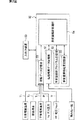
上記処理装置10は,例えば図2に示すように,運転データ及び処理結果データを統計的に処理する多変量解析装置50と,処理結果データを入力すると共に解析結果等の情報を出力する入出力装置60とを備える。処理装置10は多変量解析装置50を介して運転データ及び処理結果データを多変量解析して両者の相関関係を求めた後,必要に応じて解析結果等の情報を入出力装置60から出力する。
上記多変量解析装置50は,図2に示すように,運転データ記憶部51,処理結果データ記憶部52,多変量解析プログラム記憶部53,多変量解析処理部54及び多変量解析結果記憶部55を備えている。
上記運転データ記憶部51は運転データを記憶する手段を構成し,上記処理結果データ記憶部52は処理結果データを記憶する手段を構成する。多変量解析処理部54は運転データと処理結果データとの相関関係(例えば予測式,回帰式)を求める手段と相関関係に基づいて処理結果を予測する手段を構成する。多変量解析結果記憶部55は多変量解析処理部54により求めた相関関係を記憶する手段を構成する。
上記多変量解析装置50は例えば多変量解析プログラム記憶部53からのプログラムに基づいて動作するマイクロプロセッサなどで構成してもよい。上記運転データ記憶部51,処理結果データ記憶部52,多変量解析結果記憶部55はそれぞれメモリなどの記録手段で構成してもよく,またハードディスクなどの記録手段にそれぞれのメモリ領域を設けて構成してもよい。
多変量解析装置50は,運転データ及びプロセス特性データの入力によりそれぞれのデータを運転データ記憶部51及び処理結果データ記憶部52で記憶した後,これらのデータ及び多変量解析プログラム記憶部53のプログラムを多変量解析処理部54に取り出し,多変量解析処理部54において運転データ及びプロセス特性データの多変量解析を行い,その処理結果を多変量解析結果記憶部55で記憶する。
ここで,運転データとはウエハWを処理する際の処理装置10に付設された複数の測定器それぞれから得られる検出データを意味し,処理結果データとはウエハWを処理した結果得られるウエハWに関するプロセス特性データ,処理室1内の状態に関する装置状態データを意味する。運転データはウエハWを処理する間に間欠的に測定し,処理結果データはウエハの処理後に必要に応じて測定する。これらの測定結果はそれぞれの記憶部51,52に記憶される。
第1の実施形態では運転データと処理結果データの相関関係を求める関係上,運転データとして処理結果に影響し易いデータを用いることが好ましい。第1の実施形態では運転データとしては処理室1内の複数箇所の温度,バックサイドガスの圧力,処理装置10の電気的データを用いている。
第1の実施形態では処理結果データのうちプロセス特性データとしては例えば表面にシリコン酸化膜を有するウエハWのシリコン酸化膜の削れ量またはこの削れ量の面内均一性を含むエッチングに関するデータを用いている。
処理結果データのうち装置状態データとしては処理室1内の副生成物の堆積膜厚,フォーカスリング10a等の部品の消耗量を含む装置状態を示すデータ等を用いることができる。第1の実施形態では処理結果データのうちプロセス特性データを用いており,その中でもウエハWの削れ量の面内均一性を用いている。
処理室1内の温度としては,第1の実施形態では上部電極であるシャワーヘッド4の温度,処理室1の内壁面の温度及び下部電極2の温度を用いている。特に下部電極2の温度の影響が大きい。これらの温度はそれぞれの部位に配置された熱電対等の従来公知の温度センサ(図示せず)を介して測定することができる。より具体的には処理室1内の温度として,上述したそれぞれの部位における一枚のウエハを処理する間の平均温度を用いている。
処理室1内の圧力としては,例えば処理室1内のプロセスガスの圧力やHeガス等のバックサイドガスの圧力を用いることができる。第1の実施形態では処理室1内の圧力としてバックサイドガスの圧力を用いている。
処理装置10の電気的データとしては,例えば高周波電源7から印加する高周波電力の基本波,高調波の電圧,電流,位相,インピーダンス等を用いることができる。第1の実施形態では整合器7A内の測定器(図示せず)により測定される整合器7Aの出力側の高周波電圧(RF電圧)Vppを用いている。高周波電圧Vppが例えば図7に示すように60時間付近で瞬間的に大きく変動することがあっても予測値に反映することができる。
プロセス特性データとして用いられるウエハWのシリコン酸化膜の削れ量の面内均一性は,例えば処理前後のウエハWの面内の13点におけるシリコン酸化膜の膜厚を測定してこれらの膜厚間の差のバラツキから得られる面内の均一性を示すデータを用いている。面内均一性は,(最大値−測定値の最小値)/(2×測定値の平均値)から求めたものを使用する。
第1の実施形態において上記多変量解析装置50は,複数種の運転データを説明変量(説明変数)とし,プロセス特性データを被説明変量(目的変量,目的変数)とする下記▲1▼の関係式(回帰式などの予測式,モデル)を多変量解析プログラムを用いて求める。下記▲1▼の回帰式において,Xは説明変量の行列を意味し,Yは被説明変量の行列を意味する。また,Bは説明変量の係数(重み)からなる回帰行列であり,Eは残差行列である。
Y=BX+E・・・▲1▼
第1の実施形態において上記▲1▼を求める際には,例えばJOURNAL OF CHEMOMETRICS,VOL.2(PP211−228)(1998)に掲載されているPLS(Partial Least Squares)法を用いている。このPLS法は,行列X,Yそれぞれに多数の説明変量及び被説明変量があってもそれぞれの少数の実測値があればXとYの関係式を求めることができる。しかも,少ない実測値で得られた関係式であっても安定性及び信頼性の高いものであることもPLS法の特徴である。
多変量解析プログラム記憶部53にはPLS法用のプログラムが記憶され,多変量解析処理部54において運転データ及びプロセス特性データをプログラムの手順に従って処理し,上記▲1▼式を求め,この結果を多変量解析結果記憶部55で記憶する。従って,第1の実施形態では上記▲1▼式を求めれば,後は運転データを説明変量として行列Xに当てはめることによってプロセス特性を予測することができる。しかもこの予測値は信頼性の高いものになる。
例えば,XTY行列に対してi番目の固有値に対応する第i主成分はtiで表される。行列Xはこの第i主成分の得点tiとベクトルpiを用いると下記の▲2▼式で表され,行列Yはこの第i主成分の得点tiとベクトルciを用いると下記の▲3▼式で表される。なお,下記の▲2▼式,▲3▼式において,Xi+1,Yi+1はX,Yの残差行列であり,XTは行列Xの転置行列である。以下では指数Tは転置行列を意味する。
X=t1p1+t2p2+t3p3+・・+tipi+Xi+1・・・▲2▼
Y=t1c1+t2c2+t3c3+・・+tici+Yi+1・・・▲3▼
而して,第1の実施形態で用いられるPLS法は,上記式▲2▼,▲3▼を相関させた場合の複数の固有値及びそれぞれの固有ベクトルを少ない計算量で算出する手法である。
PLS法は以下の手順で実施される。先ず第1段階では,行列X,Yのセンタリング及びスケーリングの操作を行う。そして,i=1を設定し,X1=X,Y1=Yとする。また,u1として行列Y1の第1列を設定する。尚,センタリングとは各行の個々の値からそれぞれの行の平均値を差し引く操作であり,スケーリングとは各行の個々の値をそれぞれの行の標準偏差で除する操作(処理)である。
第2段階では,wi=Xi Tui/(ui Tui)を求めた後,wiの行列式を正規化し,ti=Xiwiを求める。また,行列Yについても同様の処理を行って,ci=Yi Tti/(ti Tti)を求めた後,ciの行列式を正規化し,ui=Yici/(ci Tci)を求める。
第3段階ではXローディング(負荷量)pi=Xi Tti/(ti Tti),Y負荷量qi=Yi Tui/(ui Tui)を求める。そして,uをtに回帰させたbi=ui Tti/(ti Tti)を求める。次いで,残差行列Xi=Xi−tipi T,残差行列Yi=Yi−bitici Tを求める。そして,iをインクリメントしてi=i+1を設定し,第2段階からの処理を繰り返す。これら一連の処理をPLS法のプログラムに従って所定の停止条件を満たすまで,あるいは残差行列Xi+1がゼロに収束するまで繰り返し,残差行列の最大固有値及びその固有ベクトルを求める。
PLS法は残差行列Xi+1の停止条件またはゼロへの収束が速く,10回程度の計算の繰り返すだけで残差行列が停止条件またはゼロに収束する。一般的には4〜5回の計算の繰り返しで残差行列が停止条件またはゼロへの収束する。この計算処理によって求められた最大固有値及びその固有ベクトルを用いてXTY行列の第1主成分を求め,X行列とY行列の最大の相関関係を知ることができる。
次に,上記処理装置10の動作を本発明方法の一実施形態と共に説明する。第1の実施形態ではまず多変量解析によってプロセス特性を予測するための上記▲1▼式を求めた後,所定のウエハWを処理する。ウエハWの処理段階では任意の時点における運転データを▲1▼式に当てはめることでその時のプロセス特性を予測することができる。
処理装置10の運転を開始すると,支持体3がボールネジ機構12を介して処理室1の下室1Bまで下降すると共に,ゲートバルブ6が開放した出入口からウエハWを搬入して下部電極2上に載置する。ウエハWの搬入後,ゲートバルブ6が閉じると共に排気系19が作動して処理室1内を所定の真空度に維持する。この際,ガス導入機構15からHeガスをバックガスとして供給し,ウエハWと下部電極2,具体的には静電チャック8とウエハW間の熱伝導性を高めてウエハWの冷却効率を高める。
一方,プロセスガス供給系18からC4F8ガスを16sccmの流量,O2ガスを300sccmの流量で供給する。また,Arガスも40sccmの流量で供給する。この時の処理室1内の圧力は例えば53mTorrである。この状態で,高周波電源7から高周波電力を1700Wで印加すると,ダイポールリング磁石5の作用と相俟ってマグネトロン放電が発生し,プロセスガスのプラズマを生成してウエハWの酸化膜をエッチングする。エッチング終了後には搬入時とは逆の操作で処理後のウエハWを処理室1内から搬出し,後続のウエハWに対して同様の処理を繰り返し,所定の枚数を処理して一連の処理を終了する。
第1の実施形態では実際のウエハWを処理する前に,実際のウエハWと同一の6枚のウエハWと19枚のダミーウエハを混ぜた25枚のウエハを1ロットとし3[分/ウエハ]の処理時間で処理し,11ロット分を10時間毎あるいは5時間毎に繰り返し処理し,6枚のウエハWに関する運転データ及びプロセス特性データを得て多変量解析を行う。第1の実施形態ではデータ数が少なくて済むPLS法を用いるため,例えば2番目及び11番目のロットにおけるウエハWの運転データ及びプロセス特性データのみを使用し,PLS法を用いてこれらのデータから上記▲1▼式を求める。尚,6枚のウエハWは各ロットの1枚目から3枚目,5枚目,10枚目及び25枚目に挿入してある。
このようなウエハWの処理を行っている間,運転データとしてシャワーヘッド(上部電極)4,処理室1の上室1Aの壁面,下部電極2それぞれの温度をそれぞれ間欠的に検出し,これらの検出信号T1,T2,T3をA/D変換器を介して多変量解析装置50へ逐次入力し,運転データ記憶部51で記憶する。
また他の運転データとしてHeガスの圧力を間欠的に検出し,この検出信号PをA/D変換器を介して多変量解析装置50へ逐次入力し,これらの入力値に基づいて多変量解析処理部54を介して標準偏差を算出し,運転データ記憶部51で記憶する。
さらに他の運転データとして高周波電源7の電圧を間欠的に検出し,この検出信号VをA/D変換器を介して多変量解析装置50へ逐次入力し,運転データ記憶部51で記憶する。
次いで,Heガス圧力以外に関してはそれぞれの運転データの各ウエハW毎の平均値を,Heガス圧力に関しては運転データの各ウエハW毎の標準偏差を多変量解析処理部54を介して求める。
次に,各ウエハW毎のそれぞれの運転データの平均値及び標準偏差を運転データ記憶部51で記憶し,あるいはそのまま次の処理に備える。
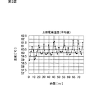
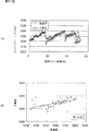
ここで,全てのウエハWの上部電極温度の検出信号T1,壁面温度の検出信号T2,下部電極温度の検出信号T3それぞれの平均値の経時変化を図示したものを図3〜図5に示す。Heガスの検出信号Pの標準偏差の経時変化を示したものを図6に示し,高周波電力の検出信号Vの平均値の経時変化を示したものを図7に示す。
そして,処理後のウエハWを取り出し,このウエハWのシリコン酸化膜の面内の13点の削れ量を入出力装置60から多変量解析装置50へ入力し,この入力値に基づいて多変量解析処理部54を介して面内均一性を算出し,この算出値をプロセス特性データとして処理結果データ記憶部52で記憶する。このようなプロセス特性データ(面内均一性)の経時変化を示したものを図8に示す。
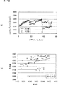
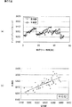
図3〜図8に示す運転データ及びプロセス特性データのうち,2番目のロットと11番目のロットの運転データ及びプロセス特性データに基づいてPLS法により上記▲1▼式の回帰行列B及び残差行列Eを求めた。そして,この式を用いて上記ロット及び上記ロット以外のロットにおけるウエハWのプロセス特性データを予測し,×印のグラフにしたものを図9に示す。また,図9の□印で示すグラフはプロセス特性データの実測値である。
図9において,2番目のロットと11番目のロットの予測値と実測値が一致しているのは▲1▼式を求める際にこの時のウエハWを使用したからである。その他のウエハWのプロセス特性データの予測値もロット毎(10時間毎)に変動する実測値に極めて近い値を示していることが判る。特に,60時間付近で大きな均一性の悪化が予測値,実測値とも確認することができる。これは,図7において確認される高周波(RF)電圧の突発的低下が反映されたものである。つまり,図3〜図6のように経時的なロット変動を検出することができきる上部電極温度,壁面温度,下部電極温度及びHeガス圧力等の処理室1内の状態を反映するデータと,図7のようにロット変動の検出は難しいが高周波電力の印加状態を反映するデータの両方を用いると有効であることが判る。
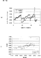
図10には,図9に示す予測値と実測値の関係をプロットして得られた相関関係を示す。この相関関係は図10からも明らかなように相関係数R=0.9053と相関性が高く予測値と実測値が概ね一致していることが判る。尚,第1の実施形態では予測値と実測値を比較するために全てのウエハWに関する運転データ及びプロセス特性データを実測したものを図3〜図9に示す。なお,このような実験の結果から第1の実施形態のプロセス特性データであるウエハWの削れ量の面内均一性の予測に際しては,特に下部電極温度の各ウエハW毎の平均値とHeガス圧力の各ウエハ毎の標準偏差を運転データとして使用することが予測精度を高めるためには重要であることがわかった。
このように本実施の形態においては,実際のウエハWを処理する前に,これと同一のウエハWを少数枚(第1の実施形態では2番目と11番目のロットの12枚)使用して上述のように運転データ及びプロセス特性データを求める。これらの少数の運転データ及びプロセス特性データを用い,PLS法によって回帰式▲1▼を求めた後,実際のウエハWを処理する場合には任意のウエハWの運転データを検出する。そして,それぞれの運転データを回帰式▲1▼に当てはめるだけで実際のウエハWの面内均一性をプロセス特性データとして予測することができる。しかも,極めて精度の高いプロセス予測を行うことができる。
以上説明したように第1の実施形態によれば,所定ロットのウエハのような少数のテストウエハを処理した時の運転データ及び処理結果データ(例えばプロセス特性データ)を収集し,これらの収集データ群(運転データ及び処理結果データ)に基づいて多変量解析を行い,この多変量解析を介して運転データと処理結果データの相関関係を求め,この相関関係に基づいてウエハの削れ量の面内均一性などのようなウエハWの処理結果(例えばプロセス特性)を予測するため,実際にウエハWを処理している時には,ウエハWの運転データを求めるだけでウエハWの面内均一性をプロセス特性として高精度に予測することができる。また,多変量解析を行って運転データと処理結果データの相関関係を求める際にPLS法を使用したため,回帰式▲1▼を短時間で効率良く求めることができる。
従って,第1の実施形態によれば,従来のように多くのテストウエハを作製したり,処理装置10を用いて多くのテストウエハを処理し,それぞれの処理結果を測定する必要がなく,テストウエハの作製及び処理結果の測定に多くの工数と時間を割く必要がない。しかも従来の予測方法よりも高精度に処理結果を予測することができる。
さらに,第1の実施形態によれば,運転データとしてプロセス特性データ(ウエハWの面内均一性)に影響し易いデータ,即ち,処理室1内の複数箇所の温度(上部電極温度,処理室1の壁面温度及び下部電極温度),処理室内の圧力(Heガスなどのバックガス圧力),電気的データ(高周波電力の電圧)を使用したため,運転データとプロセス特性データの相関関係が強く,プロセス特性を高精度で予測することができる。さらに,プロセス特性データとしてウエハWの面内均一性を採用したため,エッチングによるウエハW面内の均一性の善し悪しを高精度で予測することができる。
なお,第1の実施形態では2番目のロットと11番目のロットのテストウエハを用いて実測値と予測値の相関関係を求めたが,相関関係を求める場合には実際のプロセスでウエハWを処理している間に定期的にテストウエハを処理して相関関係を求めても良く,あるいは不定期にテストウエハを処理して相関関係を求めても良い。一度相関関係を求めた後,適宜テストウエハを用いてデータを追加して相関関係を更新することで予測精度をより高めることができる。
また,上記第1の実施形態では運転データとして上部電極温度,処理室壁面温度,下部電極温度を用いたがプロセス特性に影響し易いその他の部位の温度を用いても良く,この際少なくとも一箇所の温度を用いれば良い。特にプロセス特性データとしてウエハWの削れ量の面内均一性を予測する場合は,下部電極温度が好ましい。
また,処理室内の圧力としてHeガスの圧力を用いたがプロセスガスの圧力を用いても良い。特にプロセス特性データとしてウエハWの削れ量の面内均一性を予測する場合は,Heガスの圧力の安定性を表す標準偏差を使用することが好ましく,またHeガスのウエハWの面内圧力差(例えばバックガスをセンタ,ミドル,エッジの3系統にしたときのその圧力差など)を使用することも好ましい。
また,第1の実施形態では運転データの電気的データとして高周波電源の電圧を用いたが,高周波電源の基本波,高調波の電流,位相及びインピーダンス等を用いても良い。
また,第1の実施形態では処理結果データとしてプロセス特性データとして用い,このプロセス特性データとしてウエハWの削れ量の面内均一性を用いたが,その他のプロセス特性データとしてウエハWの削れ量の他,エッチングパターンの線幅やテーパ角度等のエッチング特性を示すデータを用いても良い。
次に,添付図面を参照しながら本発明をプラズマエッチング装置の処理結果の予測方法に適用した場合の第2の実施形態について詳細に説明する。なお,第2の実施形態において上記第1の実施形態における同一部分には同一符号を付して詳細な説明を省略する。
第2の実施形態では,運転データとするパラメータを変更又は追加して,処理結果データとしてプロセス特性データのうちのウエハWの削れ量(例えばエッチングレート)を用いて多変量解析を行い,ウエハWのエッチングレートを予測する。
先ず,第2の実施形態にかかるプラズマエッチング装置としてマグネトロン反応性エッチング処理装置(以下,「処理装置100」と称す。)について図11を参照しながら説明する。なお,図11において図1と同一部分には同一符号を付して詳細な説明を省略する。
図11に示す処理装置100のシャワーヘッド4には,処理室1内のプラズマ発光を検出する分光器(以下,「光学計測器」と称す。)20が設けられている。この光学計測器20によって得られる特定の波長範囲(例えば200〜950nm)の発光スペクトル強度を光学的データとする。
ガス導入部4Aには,配管17を介してプロセスガス供給系18′が接続されている。プロセスガス供給系18′は,C5F8ガス供給源18A′,O2ガス供給源18D′,Arガス供給源18G′を有している。
これらのガス供給源18A′,18D′,18G′はそれぞれバルブ18B′,18E′,18H′及びマスフローコントローラ18C′,18F′,18I′を介してそれぞれのガスを所定の流量でシャワーヘッド4へ供給し,その内部で所定の配合比を持った混合ガスとして調整する。各ガス流量はそれぞれのマスフローコントローラ18C′,18F′,18I′によって検出可能である。第2の実施形態では各ガス流量のうちC5F8ガスのガス流量とArガスのガス流量を検出する。検出されたこれらのガス流量のデータはトレースデータとされる。
排気管1Cには,APC(Auto Pressure Controller)バルブ1Dが設けられており,処理室1内のガス圧力に即してAPCバルブの開度が自動的に調節される。第2の実施形態ではAPCバルブ1DによるAPC開度を検出する。検出されたAPC開度はトレースデータとされる。
静電チャック8の電極板8Aと直流電源9との間には,静電チャック8の印加電流,印加電圧を検出する電力計9aが接続されている。この電力計9aから検出された静電チャック8の印加電流,印加電圧のデータはトレースデータとされる。
バックサイドガス(例えばHeガス)を導入するガス導入機構15には例えばマスフローコントローラ(図示せず)が設けられており,このマスフローコントローラによりバックサイドガスのガス流量を検出する。バックサイドガスのガス流量は,圧力計15Bにより検出されるバックサイドガスのガス圧力とともに,トレースデータとされる。
上記整合器7Aは例えば2個の可変コンデンサC1,C2,コンデンサC及びコイルLを内蔵し,可変コンデンサC1,C2を介してインピーダンス整合を取っている。整合状態での可変コンデンサC1,C2のポジションはトレースデータとされる。
上記整合器7Aは電力計7aを設け,この電力計7aにより高周波電力の供給ライン(電線)と処理装置100のグランド(接地)との間の電圧Vdcを計測する。この高周波電力供給ライン(電線)と接地間の電圧Vdcはトレースデータとされる。
上記整合器7Aの下部電極2側(高周波電圧の出力側)には電気計測器(例えば,VIプローブ)7Cが取り付けられ,この電気計測器7Cを介して下部電極2に印加される高周波電力Pにより上室1A内に発生するプラズマに基づく基本波(高周波電力の進行波及び反射波)及び高調波の高周波電圧V,高周波電流I,高周波位相P,インピーダンスZを電気的データとして検出する。このうち高周波電力の進行波及び反射波はトレースデータとされる。また高調波の高周波電圧V,高周波電流I,高周波位相P,インピーダンスZはVIプローブデータとされる。
高周波電源7と電力計7Bとの間には,高周波電力の印加時間を積算する積算部7bが接続されている。この積算部7bにより検出された高周波電力の印加積算時間もトレースデータとされる。ここでいう印加積算時間は,ウエハWを処理するごとに高周波電力を印加する時間を積算したものである。
積算部7bは,処理装置100のメンテナンスを行うごとに上記高周波電力の印加積算時間をゼロにリセットするようになっている。従って,ここでいう高周波電力の印加積算時間は,次のメンテナンスを行うまでの印加積算時間となる。
上記メンテナンスとしては,例えばエッチングにより生じた処理装置100内の副生成物(例えばパーティクル)を除去する等のために行うウエットクリーニング,消耗品や測定器の交換などがある。第2の実施形態ではウエットクリーニングを行うごとに印加積算時間をゼロにリセットするようにしている。
次に,第2の実施形態における多変量解析装置50のブロック図を図12に示す。第2の実施形態では,各測定器から検出された運転データを光学データ,トレースデータ,VIプローブデータに分けて用いる。光学データとしては,上述した光学計測器20から検出される例えば200〜950nmの波長範囲の発光スペクトル強度を用いる。
トレースデータとしては,第1の実施形態で説明した処理室1内の複数箇所の温度(上部電極温度T1,壁面温度T2,下部電極温度T3),バックサイドガスの圧力,整合器7Aの出力側の高周波電圧(RF電圧)Vppのデータに,さらに次のデータを加えて用いる。
すなわち処理ガスであるC5F8ガスとArガスのガス流量,バックサイドガスの流量,APCバルブ1DによるAPC開度,静電チャック8の印加電流及び印加電圧,整合器7Aにおける可変コンデンサC1,C2のポジション,整合器7Aにおける高周波電力供給ラインと接地間の電圧Vdc,高周波電力の進行波及び反射波のデータ,高周波電力の印加積算時間をトレースデータに加える。なお,バックサイドガスの圧力,流量としては,それぞれ例えばウエハWのセンタとエッジにおける流量を用いる。
VIプローブデータとしては,高調波の高周波電圧V,高周波電流I,高周波位相P,インピーダンスZを用いる。プロセス特性データとしては,ウエハWの削れ量を用いる。具体的にはウエハWのウエハWの削れ量として,ウエハW表面に例えばCVD(化学気相成長法)により形成されたCVD酸化膜をエッチング処理した際のエッチングレート(Å/min)のデータを用いる。
第2の実施形態における多変量解析装置50では,上記運転データのうち例えば光学データ等を説明変数とし,処理結果データとしてプロセス特性データの1つであるウエハWのエッチングレートを被説明変量(目的変量)として,上述した第1の実施形態で説明した回帰式(▲1▼の関係式)を例えばPLS法用の多変量解析プログラムを用いて求める。そして,求めた回帰式に運転データを入力してウエハWのエッチングレートを予測する。
第2の実施形態における多変量解析処理部54では,▲1▼の関係式(回帰式)の算出等の多変量解析を行う前に,運転データ及び処理結果データに対して前処理を行うようになっている。前処理としては例えばOSC(Orthogonal Signal Correction),MSC(Multiplicative Signal Correction),SNV(Standard Normal Variate Transformation)のいずれかを選択的に行うことができるようになっている。
上記OSCによる前処理は一般的には,目的変数Yに関係ない成分(Yと垂直成分)を説明変数Xから取り除く前処理である。なお,上記OSCによる前処理についての詳細は例えばWold,et al.,(1998a),orthogonal Signal Correction of Near−Infrared Spectra,Chemometrics and Intelligent Laboratory Systems,44,175−185.に掲載されている。
上記SNVによる前処理は一般的には,サンプル(ここではウエハWごとの運転データ及び処理結果データ)のばらつきの影響を校正するためにサンプル毎にデータ方向に基準化を行う前処理である。具体的には上記SNVによる前処理は例えば各サンプルを標準偏差で基準化することにより補正を行う。なお,上記SNVによる前処理についての詳細は例えばBarnes,et al.,(1989),Standard Normal Variate Transformation and De−trending on Near−Infrared Diffuse Reflectance Spectra,Applied Spectroscopy,43,772−777.に掲載されている。
上記MSCによる前処理は一般的には,サンプルから理想スペクトルを得ることにより,サンプル間の分散がより小さくなるよう補正する前処理である。具体的には上記MSCによる前処理は例えばサンプル毎に波長方向に平均を算出(理想スペクトル)し,各サンプルに対して理想スペクトルとの線形回帰直線を算出する。線形回帰直線から得られる傾きと切片より,各サンプルのデータを補正する。なお,上記MSCによる前処理についての詳細は例えばGelad,et al.,(1985),Linearization and Scatter−infrared Reflactance Spectra of Meat,Applied Spectroscopy,3,491−500.に記載されている。
次に,第2の処理装置100の動作について説明する。処理装置100の運転を開始すると,光学計測器20などの各測定器から間欠的に検出された検出データは,多変量解析装置50へ逐次入力される。ここで,エッチング処理の際の条件は,処理室内の圧力を50mT,下部電極に印加する高周波電力を1500W,処理ガスをC5F8とO2とArとの混合ガス,バックサイドガスをHeガスとした。
続いて,それぞれの運転データの各ウエハW毎の平均値を多変量解析処理部54を介して求める。次いで,各ウエハW毎のそれぞれの運転データの平均値を運転データ記憶部51で記憶し,あるいはそのまま次の処理に備える。
そして,処理後のウエハWを取り出し,このウエハWのCVD酸化膜のエッチングレートを入出力装置60から多変量解析装置50へ入力し,この入力値をプロセス特性データとして処理結果データ記憶部52で記憶する。そして前処理を行わず又は前処理を行ってからPLS法による回帰式(▲1▼の関係式)を求める。
ここで,ウエハWの処理枚数と測定したエッチングレートとの関係を図13に示す。図13においてWC(ウエットクリーニングサイクル)1は1回目の処理装置100のウエットクリーニングを行うまでの区間,WC2は1回目のウエットクリーニングを行ってから2回目のウエットクリーニングを行うまでの区間,WC3は2回目のウエットクリーニングを行ってから3回目のウエットクリーニングを行うまでの区間,WC4は3回目のウエットクリーニングを行ってから4回目のウエットクリーニングを行うまでの区間である。
上記運転データ及び処理結果データのうち,ウエットクリーニングサイクルWC1(1枚目〜16枚目)のデータに基づいてPLS法により回帰式(▲1▼の関係式)の回帰行列B及び残差行列Eを求めた。そして,この式を用いて上記WC1及び上記WC1以外のWC2(17枚目〜36枚目),WC3(37枚目〜47枚目),WC4(48枚目〜52枚目)における処理結果データであるウエハWのエッチングレートのデータを予測した。
ウエハWのエッチングレートの予測結果を□印のグラフにしたものを図14〜図29の各図(a)に示す。これらの各図(a)のうち,◇印で示すグラフはウエハWのエッチングレートのデータの実測値である。図14〜図29の各図(a)の実験結果については,それぞれ予測誤差(PE;Prediction Error)を算出した。この予測誤差PEは,各ウエハのデータの実測値から予測値を引算して2乗したものの総和を求め,これを処理したウエハ枚数で割算してその平方根を求めたものである。予測誤差PEは0が最もよく,この値が小さいほど実測値と予測値との誤差が少ないことを示す。
図14〜図29の各図(a)に示す予測値と実測値の関係をプロットして得られた相関関係をそれぞれ図14〜図29の各図(b)に示す。図14〜図29の各図(b)の実験結果については,相関係数Rを求めた。相関係数Rは1が最もよく,この値が大きいほどより相関があることを示す。従って,総合的には上記予測誤差PEが0に近く,かつ相関係数Rが1に近いほど,予測精度がよい。
なお,上記実験結果についてはWC1〜WC4とも同じエッチング条件でエッチングしているため,予測誤差PE,相関係数を求める際には,WC1〜WC4までのデータを使用している。但し,VIプローブを説明変量としたエッチングレートの実験結果(図17,図21,図25,図29)については,実験上の理由によりWC4だけ他のWC1〜WC3とはエッチング条件が異なっているため,図17,図21,図25,図29の実験結果における予測誤差PE,相関係数を求める際には,WC4のデータを除いたWC1〜WC3までのデータを使用している。
図14〜図17は,前処理を行わずにPLS法による多変量解析を行った場合の実験結果を示す。図14は,上記光学データを説明変量とした場合であり,図15は上記光学データ及び上記トレースデータを説明変量とした場合である。図16は上記トレースデータを説明変量とした場合であり,図17は上記VIプローブデータを説明変量とした場合である。
図18〜図21は,前処理として上述したOSCを行ってからPLS法による多変量解析を行った場合の実験結果を示す。図18は,上記光学データを説明変量とした場合であり,図19は上記光学データ及び上記トレースデータを説明変量とした場合である。図20は上記トレースデータを説明変量とした場合であり,図21は上記VIプローブデータを説明変量とした場合である。
図22〜図25は,前処理として上述したSNVを行ってからPLS法による多変量解析を行った場合の実験結果を示す。図22は,上記光学データを説明変量とした場合であり,図23は上記光学データ及び上記トレースデータを説明変量とした場合である。図24は上記トレースデータを説明変量とした場合であり,図25は上記VIプローブデータを説明変量とした場合である。
図26〜図29は,前処理として上述したMSCを行ってからPLS法による多変量解析を行った場合の実験結果を示す。図26は,上記光学データを説明変量とした場合であり,図27は上記光学データ及び上記トレースデータを説明変量とした場合である。図28は上記トレースデータを説明変量とした場合であり,図29は上記VIプローブデータを説明変量とした場合である。
上述した図14〜図29の各図(a)における実験結果から予測誤差PEを求めて表にまとめたものを図30に示し,図14〜図29の各図(b)における実験結果から相関係数Rを求めて表にまとめたものを図31に示す。
多変量解析に使用したデータの観点から大局的に見ると,図30によれば予測誤差PEは光学データを用いた場合が最も大きく,光学データとトレースデータを用いた場合,VIプローブデータを用いた場合,トレースデータを用いた場合の順に小さくなり,トレースデータを用いた場合が最も小さい。さらに図31によれば相関係数Rは光学データを用いた場合が最も小さく,光学データとトレースデータを用いた場合,VIプローブデータを用いた場合,トレースデータを用いた場合の順に大きくなり,トレースデータを用いた場合が最も大きい。
従って,多変量解析に使用したデータの観点から大局的に見ると,光学データを用いた場合,光学データとトレースデータを用いた場合,VIプローブデータを用いた場合,トレースデータを用いた場合の順に予測精度が向上しており,トレースデータを用いた場合が最も予測精度がよく,予測するのに有効であることがわかる。
予測精度が最もよかったトレースデータを用いた場合について,さらに前処理の有無や種類の観点から大局的に見ると,図30によれば予測誤差PEはOSCの場合を除けば,前処理をしない場合よりも前処理をした場合の方が小さい。また予測誤差PEは,前処理をした場合にはOSC,SNV,MSCの順に小さくなり,前処理としてMSCをした場合が最も小さい。さらに図31によれば相関係数RはOSCの場合を除けば,前処理をしない場合よりも前処理をした場合の方が大きい。また相関係数Rは,前処理をした場合にはOSC,SNV,MSCの順に大きくなり,前処理としてMSCをした場合が最も大きい。
従って,予測精度が最もよかったトレースデータを用いた場合について,さらに前処理の有無や種類の観点から大局的に見ると,前処理としてOSCをした場合を除けば,前処理をしない場合よりも前処理をした場合の方が予測精度がよく,有効であることがわかる。さらに前処理をした場合にはOSC,SNV,MSCの順に予測精度がよくなり,前処理としてMSCをした場合が最も予測精度がよく,有効であることがわかる。
以上により,ウエハWのエッチングレートを予測するには,説明変量としてトレースデータを用いて多変量解析を行い,さらに多変量解析に先立って前処理としてMSCを行った場合が最も予測精度がよくなり,最も有効であることがわかる。
ここで,上記トレースデータのうちのどの種類のデータが最も予測結果に影響しているかを検討する。トレースデータにおける各種類のデータについて予測結果への影響変数VIP(variable influence on projection)を求めて表にしたものを図32に示す。影響変数VIPは目的変数Yを予想したときの各説明変数X毎の影響の大きさを示すものである。例えばaをコンポーネント,Rをローディングベクトル,Wを重みベクトル,R2yをyの相関係数とすると,上記影響変数VIPは(W[a]の二乗)×(R2y[a])の各コンポーネントの総和を規格化したものとして表される。
図32によれば,影響変数VIPは整合器7Aの出力側の高周波電圧(RF電圧)Vppが最も大きく,次いで高周波電力の印加積算時間が大きい。従って,高周波電圧Vppと高周波電力の印加積算時間が予測結果に大きく影響していることがわかる。
そこで,高周波電圧Vpp,高周波電力の印加積算時間をトレースデータから除いて多変量解析を行ってウエハWのエッチングレートを予測してみると,図33〜図35に示すような実験結果が得られた。図33〜図35の各(a)にはウエハWのエッチングレートの予測結果を□印のグラフで示す。これらの各図(a)のうち,◇印で示すグラフはウエハWのエッチングレートのデータの実測値である。図33〜図35の各図(a)に示す予測値と実測値の関係をプロットして得られた相関関係をそれぞれ図33〜図35の各図(b)に示す。
図33はトレースデータから高周波電圧Vppのみを除いたデータを用いた場合,図34はトレースデータから高周波電力の印加積算時間のみを除いたデータを用いた場合,図35はトレースデータから高周波電圧Vppと高周波電力の印加積算時間を除いたデータを用いた場合である。
図33〜図35の各図(a)の実験結果についてそれぞれ予測誤差PEを算出するとそれぞれ,49.7Å/min,55.1Å/min,66.3Å/minとなった。ここで,上述したトレースデータのすべてのデータを用いた場合(図16(a))の予測誤差43.7Å/minと比較すると,図33(a)〜図35(a)のいずれの場合も図16(a)の場合よりも予測誤差が大きくなっていることがわかる。
次に図33〜図35の各図(b)の実験結果についてそれぞれ相関係数Rを算出するとそれぞれ,0.82,0.83,0.57となった。ここで,上述したトレースデータのすべてのデータを用いた場合(図16(b))の相関係数0.90と比較すると,図33(b)〜図35(b)のいずれの場合も図16(b)の場合よりも相関係数が小さくなっていることがわかる。
従って,高周波電圧Vppのみを除いたトレースデータを用いた場合(図33),高周波電力の印加積算時間のみを除いたトレースデータを用いた場合(図34),高周波電圧Vppと高周波電力の印加積算時間を除いたトレースデータを用いた場合(図36)のいずれの場合にも,トレースデータのすべてのデータを用いた場合より予測精度が低下することが確認できた。しかも高周波電圧Vppと高周波電力の印加積算時間を除いた場合が最も予測精度が悪くなることも確認できた。
従って,ウエハWのエッチングレートを予測する場合には,トレースデータとして少なくとも高周波電圧Vppを有することが有効であり,さらに高周波電力の印加積算時間を有することがより好ましい。
以上説明したように第2の実施形態によれば,1つのウエットクリーニングサイクル(WC)のウエハのような少数のテストウエハを処理した時の運転データ及び処理結果データ(例えばプロセス特性データ)を収集し,これらの収集データ群(運転データ及び処理結果データ)に基づいて多変量解析を行い,この多変量解析を介して運転データと処理結果データの相関関係を求め,この相関関係に基づいてウエハWの削れ量(例えばエッチングレート)のようなウエハWの処理結果(例えばプロセス特性)を予測するため,実際にウエハWを処理している時には,ウエハWの運転データを求めるだけでウエハWの削れ量(例えばエッチングレート)をプロセス特性として高精度に予測することができる。また,多変量解析を行って運転データと処理結果データの相関関係を求める際にPLS法を使用したため,回帰式▲1▼を短時間で効率良く求めることができる。
従って,第2の実施形態によっても,従来のように多くのテストウエハを作製したり,処理装置10を用いて多くのテストウエハを処理し,それぞれの処理結果を測定する必要がなく,テストウエハの作製及び処理結果の測定に多くの工数と時間を割く必要がない。しかも従来の予測方法よりも高精度に処理結果を予測することができる。
さらに,第2の実施形態においては,運転データとして高周波電圧Vpp,高周波電力の印加積算時間を含むトレースデータ,光学データ,VIプローブデータなどプロセス特性データに影響し易いデータを第1の実施形態で用いたデータにさらに追加することにより,プロセス特性データの予測精度をより向上させることができる。
特にプロセス特性データとしてのウエハWの削れ量(例えばエッチングレート)に影響し易い高周波電圧Vpp,高周波電力の印加積算時間を含むトレースデータを使用することにより,ウエハWの削れ量の予測精度をより向上させることができる。
また,多変量解析を行うのに先立って所定の前処理を行うことにより,より一層プロセス特性データの予測精度を向上させることができる。
また,プロセス特性データとしてウエハWのエッチングレートを採用したため,エッチングによるウエハWのエッチングの善し悪しを高精度で予測することができる。
上述したように光学データやVIプローブデータを運転データとして用いても予測精度は向上する。ところが,例えば図13に示すウエットクリーニングサイクルなどのメンテナンスを行った前後のようにプロセス特性データ(例えばエッチングレート)の傾向が大きく変化するような場合には,予測精度が低下する場合がある。例えば図14,図17では多変量解析による回帰式(モデル)を作成したウエットクリーニングサイクル(WC1)以外のウエットクリーニングサイクル(WC3)では予測精度が低下している。この点,高周波電圧Vpp,高周波電力の印加積算時間を含むトレースデータを運転データとして用いれば,図16に示すようにすべてのウエットクリーニングサイクル(WC2〜WC4)において予測精度を向上できる。
特に,トレースデータの高周波電力の印加積算時間については,例えばウエットクリーニングなどのメンテナンスを行うごとに印加積算時間をゼロにすることから,ウエットクリーニングサイクルごとの印加積算時間のデータを得ることができる。このため高周波電力の印加積算時間を運転データとして用いると,ウエットクリーニングを行うことによって傾向が変るような処理結果データであっても高い精度で予測をすることができる。
このように,本発明によれば,少数の試料を処理して得られる少数の運転データ及びプロセス特性データを収集するだけでプロセス特性の予測式を求めることができ,その後は被処理体を処理した時の運転データを予測式に当てはめるだけでプロセス特性を簡単且つ高精度に予測することができる処理結果の予測方法を提供することができる。
以上,本発明の好適な実施の一形態について,添付図面を参照しながら説明したが,本発明はかかる構成に限定されるものではない。特許請求の範囲に記載された技術的思想の範疇において,当業者であれば,各種の変更例および修正例に想到し得るものであり,それら変更例および修正例についても本発明の技術的範囲に属するものと了解される。
例えば上記第2の実施形態では処理結果データとしてプロセス特性データとして用い,このプロセス特性データとしてウエハWの削れ量(例えばエッチングレート)を用いたが,その他のプロセス特性データとしてエッチングパターンの線幅やテーパ角度等のエッチング特性を示すデータを用いてもよい。
また,上記第1及び第2の実施形態における処理結果データとしては,処理室内の副生成物の膜厚,フォーカスリング10a等の部品の消耗量などの装置状態に関する装置状態データを用いてもよい。副生成物の膜厚,フォーカスリング10a等の部品の消耗量を装置状態データとして用いることにより,処理装置10のクリーニング時期やフォーカスリング10a等の部品の交換時期を予測することもできる。
また,上記第1及び第2の実施形態ではウエハWをエッチング処理する場合について説明したが,エッチング処理以外の成膜処理等の処理装置にも本発明を適用することができる。また,被処理体のウエハに制限されるものではない。
また,上記第1及び第2の実施形態では多変量解析を行う際にPLS法を用いて回帰式▲1▼を求めたが,PLS法以外の他の従来公知の数値計算手法(例えば,ベキ乗法等)を用いて固有値及びその固有ベクトルを求めても良い。
産業上の利用の可能性
本発明は,例えば半導体製造装置で処理するウエハなどの被処理体や装置状態の処理結果を予測する方法および処理装置に適用可能であり,特にプラズマエッチングを行うプラズマ処理装置およびこのような装置における処理結果の予測方法に適用可能である。
【図面の簡単な説明】
図1は本発明における予測方法を適用する第1の実施の形態にかかる処理装置を示す断面図である。
図2は同実施形態にかかる多変量解析装置の一例を示すブロック図である。
図3は図2に示す多変量解析装置で得られた上部電極温度の経時変化を示すグラフである。
図4は図2に示す多変量解析装置で得られた処理室の壁面温度の経時変化を示すグラフである。
図5は図2に示す多変量解析装置で得られた下部電極温度の経時変化を示すグラフである。
図6は図2に示す多変量解析装置で得られたHeガス圧力の標準偏差値の経時変化を示すグラフである。
図7は図2に示す多変量解析装置で得られた高周波電源の電圧の経時変化を示すグラフである。
図8は図2に示す多変量解析装置で得られたウエハWのシリコン酸化膜の削れ量の面内均一性の経時変化を示すグラフである。
図9は図3〜図8の運転データ及びプロセス特性データを用いて図2に多変量解析装置で得られたプロセス特性データの予測値及び実測値を示すグラフである。
図10は同実施形態により得られた予測値と実測値の相関関係を示すグラフである。
図11は本発明における予測方法を適用する第2の実施の形態にかかる処理装置を示す断面図である。
図12は同実施形態にかかる多変量解析装置の一例を示すブロック図である。
図13は図12に示す多変量解析装置で得られたウエハWのCVD酸化膜のエッチングレートとウエハ処理枚数との関係を示すグラフである。
図14(a)は運転データとして光学データを用い,前処理をしない場合のエッチングレートの予測値及び実測値を示すグラフであり,図14(b)は予測値と実測値の相関関係を示すグラフである。
図15(a)は運転データとして光学データとトレースデータを用い,前処理をしない場合のエッチングレートの予測値及び実測値を示すグラフであり,図15(b)は予測値と実測値の相関関係を示すグラフである。
図16(a)は運転データとしてトレースデータを用い,前処理をしない場合のエッチングレートの予測値及び実測値を示すグラフであり,図16(b)は予測値と実測値の相関関係を示すグラフである。
図17(a)は運転データとしてVIプローブデータを用い,前処理をしない場合のエッチングレートの予測値及び実測値を示すグラフであり,図17(b)は予測値と実測値の相関関係を示すグラフである。
図18(a)は運転データとして光学データを用い,OSCによる前処理をした場合のエッチングレートの予測値及び実測値を示すグラフであり,図18(b)は予測値と実測値の相関関係を示すグラフである。
図19(a)は運転データとして光学データとトレースデータを用い,OSCによる前処理をした場合のエッチングレートの予測値及び実測値を示すグラフであり,図19(b)は予測値と実測値の相関関係を示すグラフである。
図20(a)は運転データとしてトレースデータを用い,OCSによる前処理をした場合のエッチングレートの予測値及び実測値を示すグラフであり,図20(b)は予測値と実測値の相関関係を示すグラフである。
図21(a)は運転データとしてVIプローブデータを用い,OCSによる前処理をした場合のエッチングレートの予測値及び実測値を示すグラフであり,図21(b)は予測値と実測値の相関関係を示すグラフである。
図22(a)は運転データとして光学データを用い,SNVによる前処理をした場合のエッチングレートの予測値及び実測値を示すグラフであり,図22(b)は予測値と実測値の相関関係を示すグラフである。
図23(a)は運転データとして光学データとトレースデータを用い,SNVによる前処理をした場合のエッチングレートの予測値及び実測値を示すグラフであり,図23(b)は予測値と実測値の相関関係を示すグラフである。
図24(a)は運転データとしてトレースデータを用い,SNVによる前処理をした場合のエッチングレートの予測値及び実測値を示すグラフであり,図24(b)は予測値と実測値の相関関係を示すグラフである。
図25(a)は運転データとしてVIプローブデータを用い,SNVによる前処理をした場合のエッチングレートの予測値及び実測値を示すグラフであり,図25(b)は予測値と実測値の相関関係を示すグラフである。
図26(a)は運転データとして光学データを用い,MSCによる前処理をした場合のエッチングレートの予測値及び実測値を示すグラフであり,図26(b)は予測値と実測値の相関関係を示すグラフである。
図27(a)は運転データとして光学データとトレースデータを用い,MSCによる前処理をした場合のエッチングレートの予測値及び実測値を示すグラフであり,図27(b)は予測値と実測値の相関関係を示すグラフである。
図28(a)は運転データとしてトレースデータを用い,MSCによる前処理をした場合のエッチングレートの予測値及び実測値を示すグラフであり,図28(b)は予測値と実測値の相関関係を示すグラフである。
図29(a)は運転データとしてVIプローブデータを用い,MSCによる前処理をした場合のエッチングレートの予測値及び実測値を示すグラフであり,図29(b)は予測値と実測値の相関関係を示すグラフである。
図30は図14〜図29の各図(a)における実験結果から予測誤差PEをまとめた表である。
図31は図14〜図29の各図(b)における実験結果から相関係数Rをまとめた表である。
図32はトレースデータにおける各種類のデータについて予測結果への影響変数VIPをまとめた表である。
図33(a)はトレースデータから高周波電圧Vppのみを除いたデータを用いた場合のエッチングレートの予測値及び実測値を示すグラフであり,図33(b)は予測値と実測値の相関関係を示すグラフである。
図34(a)はトレースデータから高周波電力の印加積算時間のみを除いたデータを用いた場合のエッチングレートの予測値及び実測値を示すグラフであり,図34(b)は予測値と実測値の相関関係を示すグラフである。
図35(a)はトレースデータから高周波電圧Vppと高周波電力の印加積算時間を除いたデータを用いた場合のエッチングレートの予測値及び実測値を示すグラフであり,図35(b)は予測値と実測値の相関関係を示すグラフである。Technical field
The present invention relates to a prediction method and a processing apparatus for a processing result of an object to be processed such as a wafer to be processed by a semiconductor manufacturing apparatus and a device state.
Background art
Various processing apparatuses are used in the semiconductor manufacturing process. For example, a processing apparatus such as a plasma processing apparatus is widely used in a film forming process or an etching process of an object to be processed such as a semiconductor wafer or a glass substrate. Each processing apparatus has unique process characteristics for the object to be processed. Therefore, for example, when performing an etching process on an object to be processed (for example, a semiconductor wafer) using an individual processing apparatus, for example, a test wafer is prepared in advance, and the test wafer is periodically etched. Based on the result (for example, the amount of chipping of the test wafer), the state of the processing apparatus at that time is determined.
However, in the method of judging the state of the processing apparatus from time to time based on the test wafer, it is necessary to produce many test wafers. Moreover, it is necessary to process many test wafers using the processing equipment and measure each processing result each time, so that it takes a lot of man-hours and time to prepare the test wafer and measure the processing results. There was a problem.
Japanese Patent Laid-Open No. 10-125660 proposes a process monitoring method for a plasma processing apparatus. This method uses a trial wafer before processing to create a model equation that correlates the plasma processing characteristics with an electrical signal that reflects the plasma state, and uses the detected value of the electrical signal obtained when processing an actual wafer as the model equation. Substituting to predict plasma processing characteristics.
Although this method is excellent in that it can predict plasma processing characteristics, it is highly accurate in actual wafer processing that includes lot fluctuations over time and sudden fluctuations in the application state of high-frequency power. Is not enough and further improvement is needed.
The present invention has been made in view of the above-mentioned problems of the prior art, and a process characteristic prediction formula (only by collecting a small number of operation data and process characteristic data obtained by processing a small number of samples ( Providing a processing result prediction method and processing device that can easily and accurately predict process characteristics by simply applying the operation data when the workpiece is processed to the prediction formula. The purpose is to do.
Disclosure of the invention
In order to solve the above problems, according to the first aspect of the present invention, a plurality of objects to be processed (for example, semiconductor wafers) are processed one by one (for example, an etching process) in a processing chamber of a processing apparatus such as a plasma processing apparatus. In the process of predicting the processing result based on the operation data and the processing result data of the processing device, the step of collecting the operation data and the processing result data, the collected operation data and the processing Result data (a step of performing multivariate analysis based on a data group, a step of obtaining a correlation between the operation data and the processing result data through the multivariate analysis, and obtaining the correlation based on the correlation. And a process for predicting the processing result using the operation data when the object to be processed other than the object to be processed is processed. .
In order to solve the above problems, according to the second aspect of the present invention, in the process of processing a plurality of objects to be processed (for example, semiconductor wafers) one by one (for example, an etching process) in a processing chamber, A processing apparatus such as a plasma processing apparatus for predicting a processing result based on result data, for example, means for storing the operation data, means for storing the processing result data, the stored operation data and the processing result Means for performing multivariate analysis based on data, means for obtaining a correlation between the operation data and the processing result data through the multivariate analysis, means for storing the obtained correlation, and the stored correlation And means for predicting a processing result using operation data when the object to be processed other than the object to be processed having obtained the correlation based on the relationship is provided. Management apparatus.
According to the first aspect and the second aspect of the present invention, the operation data and the processing result data are obtained by multivariate analysis only by collecting a small number of operation data and processing result data obtained by processing a small number of samples, for example. (For example, a prediction formula such as a regression formula) can be obtained. Thereafter, the processing result of the object to be processed can be predicted easily and with high accuracy simply by applying the operation data when the object is processed to the correlation.
Further, if the multiple regression analysis is performed as the multivariate analysis, a regression equation which is a correlation between the operation data and the processing result data can be easily obtained even with a large number of variable data by the multiple regression analysis.
Further, if the PLS method is used when performing the multivariate analysis, a relational expression that is a correlation between the operation data and the processing result data can be easily obtained even for a large number of variable data.
Further, the operation data may include temperature data of a mounting table on which the object to be processed is mounted, and may further include back gas pressure data. The operation data easily affects the processing result data (there is a correlation), and includes the temperature data of the mounting table and the back gas pressure data, so that the prediction accuracy of the processing result can be improved.
The operation data may include standard deviation data of back gas pressure (for example, backside gas pressure such as He gas), and an in-plane pressure difference of the object to be processed (for example, back gas is centered, The pressure difference when the three systems of middle and edge are used may be included. These standard deviations of the back gas pressure represent the stability of the back gas pressure, and are particularly useful for predicting the in-plane uniformity of the scraping amount of the wafer W as the processing result data of the object to be processed. Accuracy can be improved.
Further, the operation data may include at least data on the voltage of a high frequency power supply applied when processing the object to be processed, and may include at least data on the accumulated operation time of the high frequency power supply. Further, both high frequency power supply voltage data and high frequency power supply integrated operation time data may be included. These high-frequency power supply voltage data and high-frequency power supply integrated operation time data are particularly useful for predicting the amount of wafer W to be scraped (for example, the etching rate) as the processing result data of the object to be processed. Can also be improved.
Further, the integrated operation time of the high-frequency power source may be reset to zero every time the processing chamber is maintained. With respect to the integrated application time of the high-frequency power of the trace data, for example, the integrated application time is set to zero every time maintenance such as wet cleaning is performed, so that the integrated application time data for each wet cleaning cycle can be obtained. For this reason, when the application integration time of high-frequency power is used as operation data, even processing result data whose tendency changes by performing wet cleaning can be predicted with high accuracy.
In addition, the processing result data is processing result data of an object to be processed relating to etching including data on a shaving amount of the processing object or in-plane uniformity data of the shaving amount, and the processing result is the processing result data of the processing object. The processing result of the object to be processed relating to etching including the data of the amount of shaving or the data of the in-plane uniformity of the amount of shaving may be used. According to this, for example, by collecting a small number of operation data and processing result data obtained by processing a small number of samples, the amount of scraping data or the in-plane uniformity data of the amount of scraping is obtained. The processing result of the object to be processed concerning simple etching can be predicted easily and with high accuracy.
BEST MODE FOR CARRYING OUT THE INVENTION
Hereinafter, a first embodiment in which the present invention is applied to a method for predicting a processing result of a plasma etching apparatus will be described in detail with reference to the accompanying drawings.
First, a magnetron reactive etching apparatus (hereinafter referred to as “
The
A high
A
An
The
A
A
A
These
For example, as shown in FIG. 2, the
As shown in FIG. 2, the
The operation
The
The
Here, the operation data means detection data obtained from each of a plurality of measuring devices attached to the
In the first embodiment, it is preferable to use data that easily affects the processing result as the operation data because the correlation between the operation data and the processing result data is obtained. In the first embodiment, as operation data, temperatures at a plurality of locations in the
In the first embodiment, the process characteristic data out of the processing result data includes, for example, data related to etching including the silicon oxide film scraping amount of the wafer W having a silicon oxide film on the surface or in-plane uniformity of the scraping amount. Yes.
Among the processing result data, as the apparatus state data, data indicating the apparatus state including the deposited film thickness of the by-product in the
As the temperature in the
As the pressure in the
As electrical data of the
The in-plane uniformity of the silicon oxide film scraping amount of the wafer W used as process characteristic data is measured by measuring the thickness of the silicon oxide film at 13 points in the surface of the wafer W before and after processing, for example. Data indicating the in-plane uniformity obtained from the variation in the difference between the two is used. The in-plane uniformity is obtained from (maximum value−minimum value of measurement value) / (2 × average value of measurement value).
In the first embodiment, the
Y = BX + E (1)
When obtaining the above (1) in the first embodiment, for example, JOURNAL OF CHEMOMETRICS, VOL. 2 (PP 211-228) (1998), the PLS (Partial Least Squares) method is used. In this PLS method, even if there are a large number of explanatory variables and explained variables in each of the matrices X and Y, a relational expression between X and Y can be obtained if there are a small number of actually measured values. Moreover, it is a feature of the PLS method that even a relational expression obtained with a small actual measurement value is highly stable and reliable.
A program for the PLS method is stored in the multivariate analysis program storage unit 53. The multivariate
For example, XTThe i-th principal component corresponding to the i-th eigenvalue with respect to the Y matrix is tiIt is represented by The matrix X is the score t of this i-th principal componentiAnd the vector pi are expressed by the following equation (2), and the matrix Y is the score t of the i-th principal component.iAnd vector ciIs used, it is represented by the following formula (3). In the following formulas (2) and (3), Xi + 1, Yi + 1Is a residual matrix of X and Y, and XTIs a transposed matrix of the matrix X. In the following, the index T means a transposed matrix.
X = t1p1+ T2p2+ T3p3+ ・ ・ + Tipi+ Xi + 1・ ・ ・ ▲ 2 ▼
Y = t1c1+ T2c2+ T3c3+ ・ ・ + Tici+ Yi + 1・ ・ ・ ▲ 3 ▼
Thus, the PLS method used in the first embodiment is a method of calculating a plurality of eigenvalues and respective eigenvectors when the above equations (2) and (3) are correlated with a small amount of calculation.
The PLS method is performed by the following procedure. First, in the first stage, the centering and scaling operations of the matrices X and Y are performed. Then set i = 1 and X1= X, Y1= Y. U1As matrix Y1Set the first column. The centering is an operation of subtracting the average value of each row from the individual value of each row, and the scaling is an operation (processing) of dividing the individual value of each row by the standard deviation of each row.
In the second stage, wi= Xi Tui/ (Ui Tui), WiNormalize the determinant of ti= XiwiAsk for. The same processing is performed for the matrix Y, and ci= Yi Tti/ (Ti Tti), CiNormalize the determinant ofi= Yici/ (Ci Tci)
In the third stage, X loading (load amount) pi= Xi Tti/ (Ti Tti), Y load qi= Yi Tui/ (Ui Tui) And b is a regression of u to ti= Ui Tti/ (Ti Tti) Then the residual matrix Xi= Xi-Tipi T, Residual matrix Yi= Yi-Bitici TAsk for. Then, i is incremented to set i = i + 1, and the processing from the second stage is repeated. These series of processes are performed until a predetermined stop condition is satisfied according to the program of the PLS method, or the residual matrix Xi + 1Repeat until the value converges to zero to find the maximum eigenvalue and its eigenvector of the residual matrix.
The PLS method uses the residual matrix Xi + 1The stop matrix or the convergence to zero is fast, and the residual matrix converges to the stop condition or zero just by repeating the calculation about 10 times. In general, the residual matrix converges to a stop condition or zero after repeating the
Next, the operation of the
When the operation of the
On the other hand, from the process
In the first embodiment, before processing an actual wafer W, 25 wafers in which six wafers W and 19 dummy wafers that are the same as the actual wafer W are mixed into one lot and 3 [minutes / wafer]. 11 lots are processed repeatedly every 10 hours or every 5 hours, and operation data and process characteristic data concerning six wafers W are obtained to perform multivariate analysis. In the first embodiment, since the PLS method that requires a small number of data is used, for example, only operation data and process characteristic data of the wafer W in the second and eleventh lots are used, and these data are obtained using the PLS method. The above equation (1) is obtained. The six wafers W are inserted into the first, third, fifth, tenth and 25th wafers of each lot.
During the processing of the wafer W, the temperature of the shower head (upper electrode) 4, the wall surface of the
Further, as other operation data, the pressure of He gas is intermittently detected, and this detection signal P is sequentially input to the
Further, the voltage of the high-
Next, an average value of each operation data for each wafer W is obtained for other than the He gas pressure, and a standard deviation for each wafer W of the operation data for the He gas pressure is obtained via the multivariate
Next, the average value and the standard deviation of the operation data for each wafer W are stored in the operation
Here, the detection signal T of the upper electrode temperature of all wafers W1, Wall temperature detection signal T2, Lower electrode temperature detection signal T3FIGS. 3 to 5 show changes over time in the average values. FIG. 6 shows a change with time of the standard deviation of the detection signal P of He gas, and FIG. 7 shows a change with time of the average value of the detection signal V of the high frequency power.
Then, the processed wafer W is taken out, and the amount of scraping at 13 points in the surface of the silicon oxide film of the wafer W is input from the input /
Among the operation data and process characteristic data shown in FIGS. 3 to 8, the regression matrix B and the residual of the above equation (1) are calculated by the PLS method based on the operation data and process characteristic data of the second lot and the eleventh lot. Matrix E was determined. Then, the process characteristic data of the wafer W in the lots and lots other than the lots is predicted using this equation, and a graph of x is shown in FIG. Further, a graph indicated by a square in FIG. 9 is an actual measurement value of the process characteristic data.
In FIG. 9, the predicted value and the actual measurement value of the second lot and the eleventh lot coincide with each other because the wafer W at this time is used when obtaining the equation (1). It can be seen that the predicted values of the process characteristic data of the other wafers W are very close to the actually measured values that vary from lot to lot (every 10 hours). In particular, a large deterioration in uniformity can be confirmed in both the predicted value and the actual measurement value in the vicinity of 60 hours. This reflects the sudden drop in the radio frequency (RF) voltage confirmed in FIG. That is, data reflecting the state in the
FIG. 10 shows the correlation obtained by plotting the relationship between the predicted value and the actually measured value shown in FIG. As is apparent from FIG. 10, this correlation is highly correlated with the correlation coefficient R = 0.9053, and it can be seen that the predicted value and the actually measured value almost coincide. In the first embodiment, actual operation data and process characteristic data relating to all wafers W are shown in FIG. 3 to FIG. 9 in order to compare the predicted value and the actual measurement value. When predicting the in-plane uniformity of the scraping amount of the wafer W, which is the process characteristic data of the first embodiment, from the results of such an experiment, in particular, the average value of the lower electrode temperature for each wafer W and the He gas It was found that using the standard deviation of each pressure for each wafer as operation data is important for improving the prediction accuracy.
As described above, in this embodiment, before processing the actual wafer W, a small number of the same wafers W (12 in the second and eleventh lots in the first embodiment) are used. Operation data and process characteristic data are obtained as described above. After obtaining the regression equation (1) by the PLS method using these small number of operation data and process characteristic data, operation data of an arbitrary wafer W is detected when an actual wafer W is processed. Then, the actual in-plane uniformity of the wafer W can be predicted as process characteristic data simply by applying each operation data to the regression equation (1). In addition, extremely accurate process prediction can be performed.
As described above, according to the first embodiment, operation data and processing result data (for example, process characteristic data) when a small number of test wafers such as wafers of a predetermined lot are processed are collected, and these collected data are collected. Multivariate analysis is performed based on the group (operation data and processing result data), and the correlation between the operation data and the processing result data is obtained through this multivariate analysis. In order to predict the processing result (for example, process characteristics) of the wafer W such as uniformity, when the wafer W is actually processed, the in-plane uniformity of the wafer W is processed by simply obtaining the operation data of the wafer W. The characteristics can be predicted with high accuracy. Further, since the PLS method is used when the correlation between the operation data and the processing result data is obtained by performing multivariate analysis, the regression equation (1) can be obtained efficiently in a short time.
Therefore, according to the first embodiment, there is no need to produce many test wafers as in the prior art or to process many test wafers using the
Furthermore, according to the first embodiment, the operation data is data that easily affects the process characteristic data (in-plane uniformity of the wafer W), that is, the temperatures (upper electrode temperature, processing chamber) in the
In the first embodiment, the correlation between the actual measurement value and the predicted value is obtained using the test wafers of the second lot and the eleventh lot. However, when obtaining the correlation, the wafer W is obtained by an actual process. During processing, the test wafer may be processed periodically to obtain the correlation, or the test wafer may be processed irregularly to obtain the correlation. Once the correlation is obtained, the prediction accuracy can be further improved by updating the correlation by adding data using a test wafer as appropriate.
In the first embodiment, the upper electrode temperature, the processing chamber wall temperature, and the lower electrode temperature are used as the operation data. However, the temperature of another part that easily affects the process characteristics may be used. The temperature may be used. In particular, when predicting in-plane uniformity of the scraping amount of the wafer W as process characteristic data, the lower electrode temperature is preferable.
Further, although the pressure of He gas is used as the pressure in the processing chamber, the pressure of process gas may be used. In particular, when predicting the in-plane uniformity of the scraping amount of the wafer W as the process characteristic data, it is preferable to use a standard deviation representing the stability of the He gas pressure. It is also preferable to use (for example, the pressure difference when the back gas is made into three systems of center, middle, and edge).
In the first embodiment, the voltage of the high frequency power supply is used as the electrical data of the operation data. However, the fundamental wave, harmonic current, phase, impedance, and the like of the high frequency power supply may be used.
In the first embodiment, the process result data is used as process characteristic data, and the in-plane uniformity of the scraping amount of the wafer W is used as the process characteristic data. In addition, data indicating etching characteristics such as the line width and taper angle of the etching pattern may be used.
Next, a second embodiment in the case where the present invention is applied to a method for predicting a processing result of a plasma etching apparatus will be described in detail with reference to the accompanying drawings. In the second embodiment, the same portions as those in the first embodiment are denoted by the same reference numerals, and detailed description thereof is omitted.
In the second embodiment, a parameter as operation data is changed or added, and multivariate analysis is performed using the amount of wafer W shaving (for example, etching rate) in the process characteristic data as processing result data. The etching rate is predicted.
First, a magnetron reactive etching apparatus (hereinafter referred to as “
The
A process
These
The
Between the
For example, a mass flow controller (not shown) is provided in the
The
The
An electrical measuring instrument (for example, a VI probe) 7C is attached to the
Between the high
The integration unit 7b is configured to reset the high frequency power application integration time to zero each time the
Examples of the maintenance include wet cleaning performed for removing by-products (for example, particles) in the
Next, FIG. 12 shows a block diagram of the
As the trace data, the temperature (upper electrode temperature T) at a plurality of locations in the
That is, the process gas C5F8Gas and Ar gas flow rate, backside gas flow rate, APC valve opening by APC valve 1D, applied current and voltage of
As the VI probe data, harmonic high-frequency voltage V, high-frequency current I, high-frequency phase P, and impedance Z are used. As the process characteristic data, the scraping amount of the wafer W is used. Specifically, the data of the etching rate (削 / min) when the CVD oxide film formed on the surface of the wafer W by, for example, CVD (chemical vapor deposition) is etched as the wafer W scraping amount. Use.
In the
The multivariate
The preprocessing by the OSC is generally preprocessing for removing components (Y and vertical components) that are not related to the objective variable Y from the explanatory variable X. Details of the pre-processing by the OSC are described in, for example, Wald, et al. (1998a), orthologous Signal Correction of Near-Infrared Spectra, Chemometrics and Intelligent Laboratory Systems, 44, 175-185. It is published in.
The pre-processing by the SNV is generally pre-processing that performs standardization in the data direction for each sample in order to calibrate the influence of variations in samples (here, operation data and processing result data for each wafer W). Specifically, the pre-processing by the SNV performs correction by standardizing each sample with a standard deviation, for example. For details on the pre-processing by the SNV, see Barnes, et al. (1989), Standard Normal Varyate Transformation and De-trending on Near-Infrared Diffuse Reflectance Spectra, Applied Spectroscopy, 43, 772-777. It is published in.
The preprocessing by the MSC is generally preprocessing for correcting the dispersion between samples to be smaller by obtaining an ideal spectrum from the samples. Specifically, the pre-processing by the MSC calculates, for example, an average in the wavelength direction for each sample (ideal spectrum), and calculates a linear regression line with the ideal spectrum for each sample. The data of each sample is corrected from the slope and intercept obtained from the linear regression line. Details of the pre-processing by the MSC are described in, for example, Gelad, et al. , (1985), Linearization and Scatter-infrared Refractance Spectra of Meat, Applied Spectroscopy, 3, 491-500. It is described in.
Next, the operation of the
Subsequently, an average value of each operation data for each wafer W is obtained through the multivariate
Then, the processed wafer W is taken out, the etching rate of the CVD oxide film of the wafer W is input from the input /
Here, the relationship between the number of processed wafers W and the measured etching rate is shown in FIG. In FIG. 13, WC (wet cleaning cycle) 1 is a section until the first wet cleaning of the
Of the operation data and the processing result data, the regression matrix B and the residual matrix E of the regression equation (relational expression (1)) are obtained by the PLS method based on the data of the wet cleaning cycle WC1 (first to 16th sheets). Asked. Then, using this equation, the processing result data in WC1 and WC2 other than WC1 (17th to 36th), WC3 (37th to 47th), and WC4 (48th to 52nd) The etching rate data of the wafer W is predicted.
Each of the graphs (a) in FIGS. 14 to 29 shows the results of prediction of the etching rate of the wafer W in the form of a square mark. Among these figures (a), the graphs indicated by ◇ are measured values of the etching rate data of the wafer W. Prediction errors (PE) were calculated for the experimental results in FIGS. 14 to 29 (a). This prediction error PE is obtained by subtracting the prediction value from the actual measurement value of the data of each wafer to obtain the sum of the squares and dividing the result by the number of processed wafers to obtain the square root. The prediction error PE is best at 0, and the smaller this value, the smaller the error between the actually measured value and the predicted value.
The correlations obtained by plotting the relationship between the predicted values and the actual measurement values shown in FIGS. 14A to 29A are shown in FIGS. 14B to 29B, respectively. The correlation coefficient R was calculated | required about the experimental result of each figure (b) of FIGS. The correlation coefficient R is 1 best, and the larger this value is, the more correlation there is. Therefore, generally, the prediction accuracy PE is better as the prediction error PE is closer to 0 and the correlation coefficient R is closer to 1.
As for the above experimental results, since etching is performed under the same etching conditions for WC1 to WC4, data for WC1 to WC4 is used when obtaining the prediction error PE and the correlation coefficient. However, the etching rate experimental results (FIGS. 17, 21, 25, and 29) with the VI probe as an explanatory variable are different in etching conditions from other WC1 to WC3 by WC4 for experimental reasons. Therefore, when obtaining the prediction error PE and the correlation coefficient in the experimental results of FIGS. 17, 21, 25, and 29, data from WC1 to WC3 excluding WC4 data is used.
14 to 17 show experimental results when multivariate analysis is performed by the PLS method without performing preprocessing. FIG. 14 shows a case where the optical data is an explanatory variable, and FIG. 15 shows a case where the optical data and the trace data are explanatory variables. FIG. 16 shows a case where the trace data is an explanatory variable, and FIG. 17 shows a case where the VI probe data is an explanatory variable.
18 to 21 show experimental results when multivariate analysis is performed by the PLS method after performing the OSC described above as preprocessing. FIG. 18 shows a case where the optical data is an explanatory variable, and FIG. 19 shows a case where the optical data and the trace data are explanatory variables. FIG. 20 shows a case where the trace data is an explanatory variable, and FIG. 21 shows a case where the VI probe data is an explanatory variable.
22 to 25 show experimental results when multivariate analysis is performed by the PLS method after performing the above-described SNV as preprocessing. FIG. 22 shows a case where the optical data is an explanatory variable, and FIG. 23 shows a case where the optical data and the trace data are explanatory variables. FIG. 24 shows a case where the trace data is an explanatory variable, and FIG. 25 shows a case where the VI probe data is an explanatory variable.
26 to 29 show experimental results when the multivariate analysis is performed by the PLS method after performing the above-described MSC as preprocessing. FIG. 26 shows a case where the optical data is an explanatory variable, and FIG. 27 shows a case where the optical data and the trace data are explanatory variables. FIG. 28 shows a case where the trace data is an explanatory variable, and FIG. 29 shows a case where the VI probe data is an explanatory variable.
FIG. 30 shows the prediction error PE obtained from the experimental results in FIGS. 14 to 29 described above and summarized in a table. The experimental results in FIGS. 14 to 29 in FIG. FIG. 31 shows the relationship number R obtained in a table.
From the perspective of data used for multivariate analysis, according to FIG. 30, the prediction error PE is greatest when optical data is used, and when optical data and trace data are used, VI probe data is used. In this case, the trace data becomes smaller in the order in which the trace data is used, and the trace data is the smallest in the case of using the trace data. Further, according to FIG. 31, the correlation coefficient R is smallest when optical data is used, when optical data and trace data are used, when VI probe data is used, and when trace data is used, the correlation coefficient R increases. The largest case is when trace data is used.
Therefore, when viewed from the perspective of the data used for multivariate analysis, when optical data is used, optical data and trace data are used, VI probe data is used, and trace data is used. The prediction accuracy improves in order, and it can be seen that the use of trace data provides the best prediction accuracy and is effective for prediction.
When the trace data with the highest prediction accuracy is used, from a viewpoint of the presence or type of preprocessing and the type, the prediction error PE is not preprocessed except for the OSC according to FIG. It is smaller when pre-processing is performed. The prediction error PE decreases in the order of OSC, SNV, and MSC when preprocessing is performed, and is smallest when MSC is performed as preprocessing. Further, according to FIG. 31, the correlation coefficient R is larger in the case of preprocessing than in the case of no preprocessing except in the case of OSC. The correlation coefficient R increases in the order of OSC, SNV, and MSC when preprocessing is performed, and is largest when MSC is performed as preprocessing.
Therefore, when using the trace data with the best prediction accuracy, from the viewpoint of the presence or type of preprocessing and the type of the preprocessing, except for the case where OSC is used as the preprocessing, the preprocessing is not performed. It can be seen that the processing accuracy is better and more accurate. Further, when pre-processing is performed, the prediction accuracy is improved in the order of OSC, SNV, and MSC, and when MSC is performed as pre-processing, the prediction accuracy is the highest and effective.
As described above, in order to predict the etching rate of the wafer W, the prediction accuracy is best when the multivariate analysis is performed using the trace data as the explanatory variable, and the MSC is performed as the preprocessing prior to the multivariate analysis. , The most effective.
Here, it is examined which kind of data among the trace data has the most influence on the prediction result. FIG. 32 shows a table obtained by calculating an influence variable VIP (variable influence on projection) on the prediction result for each type of data in the trace data. The influence variable VIP indicates the magnitude of the influence for each explanatory variable X when the objective variable Y is predicted. For example, if a is a component, R is a loading vector, W is a weight vector, and R2y is a correlation coefficient of y, the influence variable VIP is the sum of the components of (W [a] squared) × (R2y [a]). Is expressed as a standardized version.
According to FIG. 32, the influence variable VIP has the largest high frequency voltage (RF voltage) Vpp on the output side of the
Therefore, when the high-frequency voltage Vpp and high-frequency power application integration time are removed from the trace data and the multivariate analysis is performed to predict the etching rate of the wafer W, experimental results as shown in FIGS. 33 to 35 are obtained. It was. Each of FIGS. 33 to 35 (a) shows a prediction result of the etching rate of the wafer W with a square mark. Among these figures (a), the graphs indicated by ◇ are measured values of the etching rate data of the wafer W. The respective correlations obtained by plotting the relationship between the predicted values and the actual measurement values shown in FIGS. 33 to 35 (a) are shown in FIGS. 33 to 35 (b), respectively.
33 shows the case where data obtained by removing only the high frequency voltage Vpp from the trace data is used, FIG. 34 shows the case where data obtained by removing only the integration time of high frequency power from the trace data is used, and FIG. 35 shows the case where the high frequency voltage Vpp is obtained from the trace data. And the data excluding the integrated application time of the high frequency power.
When the prediction error PE was calculated for each of the experimental results in FIGS. 33 to 35, the results were 49.7 Å / min, 55.1 Å / min, and 66.3 Å / min, respectively. Here, in comparison with the prediction error of 43.7 mm / min when all the trace data described above is used (FIG. 16A), any of the cases shown in FIGS. 33A to 35A. It can be seen that the prediction error is larger than in the case of FIG.
Next, when the correlation coefficient R was calculated for each of the experimental results of FIGS. 33 to 35 (b), it was 0.82, 0.83, and 0.57, respectively. Here, when compared with the correlation coefficient 0.90 in the case where all of the above-described trace data is used (FIG. 16B), the case of any of FIGS. 33B to 35B is shown. It can be seen that the correlation coefficient is smaller than in the case of 16 (b).
Therefore, when the trace data excluding only the high frequency voltage Vpp is used (FIG. 33), the trace data excluding only the high frequency power application integration time is used (FIG. 34), the high frequency voltage Vpp and the high frequency power application integration. In any case where the trace data excluding time was used (FIG. 36), it was confirmed that the prediction accuracy was lower than when all the trace data was used. In addition, it was also confirmed that the prediction accuracy was worst when the high frequency voltage Vpp and the high frequency power application integration time were removed.
Therefore, when predicting the etching rate of the wafer W, it is effective to have at least the high-frequency voltage Vpp as the trace data, and it is more preferable to have the application integration time of the high-frequency power.
As described above, according to the second embodiment, operation data and processing result data (for example, process characteristic data) when a small number of test wafers such as wafers in one wet cleaning cycle (WC) are processed are collected. Then, multivariate analysis is performed based on these collected data groups (operation data and processing result data), and the correlation between the operation data and the processing result data is obtained through this multivariate analysis. In order to predict the processing result (for example, process characteristics) of the wafer W such as the amount of shaving (for example, the etching rate) of the W, when the wafer W is actually processed, the operation data of the wafer W is simply obtained. The amount of abrasion (for example, the etching rate) can be predicted with high accuracy as the process characteristics. Further, since the PLS method is used when the correlation between the operation data and the processing result data is obtained by performing multivariate analysis, the regression equation (1) can be obtained efficiently in a short time.
Therefore, according to the second embodiment, there is no need to produce many test wafers as in the prior art or to process many test wafers using the
Further, in the second embodiment, data that easily influences process characteristic data such as high-frequency voltage Vpp, trace data including the application integration time of high-frequency power, optical data, and VI probe data is used as operation data in the first embodiment. By further adding to the used data, the prediction accuracy of the process characteristic data can be further improved.
In particular, the use of trace data including the high frequency voltage Vpp, which is likely to affect the amount of wafer W shaving (for example, the etching rate) as the process characteristic data, and the integrated application time of the high frequency power further increases the prediction accuracy of the amount of shaving of the wafer W. Can be improved.
In addition, by performing predetermined preprocessing prior to performing multivariate analysis, it is possible to further improve the prediction accuracy of process characteristic data.
Further, since the etching rate of the wafer W is adopted as the process characteristic data, it is possible to predict the quality of the etching of the wafer W by etching with high accuracy.
As described above, the prediction accuracy is improved even when optical data or VI probe data is used as operation data. However, for example, when the tendency of process characteristic data (for example, etching rate) changes significantly before and after performing maintenance such as a wet cleaning cycle shown in FIG. 13, the prediction accuracy may decrease. For example, in FIGS. 14 and 17, the prediction accuracy is reduced in the wet cleaning cycle (WC3) other than the wet cleaning cycle (WC1) in which the regression equation (model) by multivariate analysis is created. In this regard, if trace data including the high frequency voltage Vpp and high frequency power application integration time is used as operation data, the prediction accuracy can be improved in all wet cleaning cycles (WC2 to WC4) as shown in FIG.
In particular, for the integrated application time of high-frequency power in the trace data, since the integrated application time is set to zero each time maintenance such as wet cleaning is performed, data of integrated application time for each wet cleaning cycle can be obtained. For this reason, when the application integration time of high-frequency power is used as operation data, even processing result data whose tendency changes by performing wet cleaning can be predicted with high accuracy.
As described above, according to the present invention, it is possible to obtain a prediction formula for process characteristics only by collecting a small number of operation data and process characteristic data obtained by processing a small number of samples, and then processing the object to be processed. Therefore, it is possible to provide a process result prediction method capable of predicting process characteristics easily and with high accuracy simply by applying the operation data at the time to the prediction formula.
The preferred embodiment of the present invention has been described above with reference to the accompanying drawings, but the present invention is not limited to such a configuration. Within the scope of the technical idea described in the claims, those skilled in the art will be able to conceive of various changes and modifications, and these changes and modifications are also within the technical scope of the present invention. It is understood that it belongs to.
For example, in the second embodiment, the process result data is used as the process characteristic data, and the amount of wafer W (for example, the etching rate) is used as the process characteristic data. However, as the other process characteristic data, the line width of the etching pattern, Data indicating etching characteristics such as a taper angle may be used.
Further, as the processing result data in the first and second embodiments, apparatus state data relating to the apparatus state such as the film thickness of by-products in the processing chamber and the consumption amount of components such as the
In the first and second embodiments, the case where the wafer W is etched has been described. However, the present invention can also be applied to a processing apparatus such as a film forming process other than the etching process. Further, the present invention is not limited to the wafer to be processed.
In the first and second embodiments, the regression equation (1) is obtained using the PLS method when performing multivariate analysis. However, other conventionally known numerical calculation methods other than the PLS method (eg, power The eigenvalue and its eigenvector may be obtained using a multiplication method or the like.
Industrial applicability
INDUSTRIAL APPLICABILITY The present invention is applicable to a method and a processing apparatus for predicting a processing result of an object to be processed such as a wafer to be processed in a semiconductor manufacturing apparatus and the state of the apparatus. The present invention can be applied to a processing result prediction method.
[Brief description of the drawings]
FIG. 1 is a sectional view showing a processing apparatus according to a first embodiment to which a prediction method according to the present invention is applied.
FIG. 2 is a block diagram showing an example of a multivariate analyzer according to the embodiment.
FIG. 3 is a graph showing the change with time of the upper electrode temperature obtained by the multivariate analyzer shown in FIG.
FIG. 4 is a graph showing the change over time in the wall temperature of the processing chamber obtained by the multivariate analyzer shown in FIG.
FIG. 5 is a graph showing the temporal change of the lower electrode temperature obtained by the multivariate analyzer shown in FIG.
FIG. 6 is a graph showing the change over time of the standard deviation value of the He gas pressure obtained by the multivariate analyzer shown in FIG.
FIG. 7 is a graph showing the change over time of the voltage of the high-frequency power source obtained by the multivariate analyzer shown in FIG.
FIG. 8 is a graph showing the change over time in the in-plane uniformity of the silicon oxide film scraping amount of the wafer W obtained by the multivariate analyzer shown in FIG.
FIG. 9 is a graph showing predicted values and actual measurement values of process characteristic data obtained by the multivariate analyzer in FIG. 2 using the operation data and process characteristic data of FIGS.
FIG. 10 is a graph showing the correlation between the predicted value and the actually measured value obtained by the embodiment.
FIG. 11 is a cross-sectional view showing a processing apparatus according to a second embodiment to which the prediction method of the present invention is applied.
FIG. 12 is a block diagram showing an example of a multivariate analyzer according to the embodiment.
FIG. 13 is a graph showing the relationship between the etching rate of the CVD oxide film on the wafer W and the number of processed wafers obtained by the multivariate analyzer shown in FIG.
FIG. 14A is a graph showing predicted values and measured values of the etching rate when optical data is used as operation data and no preprocessing is performed, and FIG. 14B shows a correlation between the predicted values and measured values. It is a graph.
FIG. 15A is a graph showing predicted values and measured values of the etching rate when optical data and trace data are used as operation data and no preprocessing is performed, and FIG. 15B is a correlation between the predicted values and the measured values. It is a graph which shows a relationship.
FIG. 16A is a graph showing a predicted value and an actually measured value of the etching rate when trace data is used as operation data and no preprocessing is performed, and FIG. 16B shows a correlation between the predicted value and the actually measured value. It is a graph.
FIG. 17 (a) is a graph showing predicted and measured values of the etching rate when VI probe data is used as operation data and no preprocessing is performed, and FIG. 17 (b) shows the correlation between the predicted value and the actually measured value. It is a graph to show.
FIG. 18A is a graph showing a predicted value and an actual measured value of the etching rate when optical data is used as operation data and pre-processed by OSC, and FIG. 18B is a correlation between the predicted value and the actual measured value. It is a graph which shows.
FIG. 19A is a graph showing predicted and actual values of the etching rate when optical data and trace data are used as operation data and pre-processed by OSC, and FIG. 19B is a graph showing predicted and actual values. It is a graph which shows correlation of these.
FIG. 20A is a graph showing a predicted value and an actually measured value of the etching rate when trace data is used as operation data and pre-processing by OCS is performed, and FIG. 20B is a correlation between the predicted value and the actually measured value. It is a graph which shows.
FIG. 21A is a graph showing a predicted value and an actually measured value of the etching rate when VI probe data is used as operation data and pre-processing by OCS, and FIG. 21B is a correlation between the predicted value and the actually measured value. It is a graph which shows a relationship.
FIG. 22A is a graph showing the predicted value and actual value of the etching rate when optical data is used as operation data and pre-processing by SNV, and FIG. 22B is the correlation between the predicted value and the actual value. It is a graph which shows.
FIG. 23 (a) is a graph showing predicted and actual values of the etching rate when optical data and trace data are used as operation data and pre-processed by SNV, and FIG. 23 (b) is a graph showing predicted and actual values. It is a graph which shows correlation of these.
FIG. 24A is a graph showing the predicted value and measured value of the etching rate when the trace data is used as the operation data and pre-processed by SNV, and FIG. 24B is the correlation between the predicted value and the measured value. It is a graph which shows.
FIG. 25A is a graph showing a predicted value and an actually measured value of the etching rate when VI probe data is used as operation data and pre-processing by SNV, and FIG. 25B is a correlation between the predicted value and the actually measured value. It is a graph which shows a relationship.
FIG. 26 (a) is a graph showing predicted values and measured values of the etching rate when optical data is used as operation data and pre-processing by MSC is performed, and FIG. 26 (b) is a correlation between the predicted values and measured values. It is a graph which shows.
FIG. 27A is a graph showing the predicted value and actual value of the etching rate when optical data and trace data are used as operation data and pre-processing by MSC is performed, and FIG. 27B is the predicted value and actual value. It is a graph which shows correlation of these.
FIG. 28A is a graph showing a predicted value and an actual measurement value of the etching rate when trace data is used as operation data and pre-processing by MSC is performed, and FIG. 28B is a correlation between the predicted value and the actual measurement value. It is a graph which shows.
FIG. 29 (a) is a graph showing predicted and measured values of the etching rate when VI probe data is used as operation data and pre-processing by MSC is performed, and FIG. 29 (b) is a correlation between the predicted value and the actually measured value. It is a graph which shows a relationship.
FIG. 30 is a table summarizing the prediction error PE from the experimental results in FIGS. 14A to 29A.
FIG. 31 is a table summarizing the correlation coefficient R from the experimental results in FIGS. 14 to 29 (b).
FIG. 32 is a table summarizing the influence variable VIP on the prediction result for each type of data in the trace data.
FIG. 33A is a graph showing a predicted value and an actually measured value of the etching rate when using data obtained by removing only the high frequency voltage Vpp from the trace data, and FIG. 33B is a correlation between the predicted value and the actually measured value. It is a graph which shows.
FIG. 34 (a) is a graph showing a predicted value and an actually measured value of the etching rate when using data obtained by removing only the integrated application time of high-frequency power from the trace data, and FIG. 34 (b) is a graph showing the predicted value and the actually measured value. It is a graph which shows correlation of these.
FIG. 35 (a) is a graph showing a predicted value and an actually measured value of the etching rate when using data obtained by removing the high-frequency voltage Vpp and the high-frequency power application integration time from the trace data, and FIG. 35 (b) is a predicted value. It is a graph which shows the correlation of measured value.
Claims (2)
上記運転データ及び上記処理結果データを収集する工程と,
収集した上記運転データ及び上記処理結果データに基づいて多変量解析を行う工程と,
上記多変量解析を介して上記運転データと上記処理結果データの相関関係を求める工程と,
上記相関関係に基づいて上記相関関係を得た被処理体以外の上記被処理体を処理した時の運転データを用いて処理結果を予測する工程と,
を有し,
上記運転データは,上記処理室内に配設され上記被処理体を載置する載置台の温度のデータを含み、さらに上記被処理体と上記載置台との間に供給されるバックガス圧力の被処理体の面内圧力差のデータを含むことを特徴とする,処理結果の予測方法。A method for predicting a processing result based on operation data and processing result data of the plasma processing apparatus in a process of plasma processing an object to be processed in a processing chamber of the plasma processing apparatus,
Collecting the operation data and the processing result data;
Performing a multivariate analysis based on the collected operation data and the processing result data;
Obtaining a correlation between the operation data and the processing result data through the multivariate analysis;
Predicting a processing result using operation data when the object to be processed other than the object to be processed having obtained the correlation based on the correlation is obtained;
Have
The operating data, see contains the temperature data of the mounting table for placing the processing chamber is disposed in the workpiece, further a back pressure of the gas supplied between the workpiece and the mounting table A method for predicting a processing result, which includes data on an in-plane pressure difference of a workpiece .
上記運転データを記憶する手段と,
上記処理結果データを記憶する手段と,
記憶した上記運転データ及び上記処理結果データに基づいて多変量解析を行う手段と,
上記多変量解析を介して上記運転データと上記処理結果データの相関関係を求める手段と,
求めた上記相関関係を記憶する手段と,
記憶した上記相関関係に基づいて上記相関関係を得た被処理体以外の上記被処理体を処理した時の運転データを用いて処理結果を予測する手段と,
を備え,
上記運転データは,上記処理室内に配設され上記被処理体を載置する載置台の温度のデータを含み,さらに上記被処理体と上記載置台との間に供給されるバックガス圧力の被処理体の面内圧力差のデータを含むことを特徴とする処理装置。A processing apparatus for predicting a processing result based on operation data and processing result data in a process of plasma processing an object to be processed in a processing chamber,
Means for storing the operation data;
Means for storing the processing result data;
Means for performing multivariate analysis based on the stored operation data and the processing result data;
Means for obtaining a correlation between the operation data and the processing result data through the multivariate analysis;
Means for storing the obtained correlation;
Means for predicting a processing result using operation data when the object to be processed other than the object to be processed having obtained the correlation based on the stored correlation is obtained;
With
The operation data includes temperature data of a mounting table disposed in the processing chamber on which the object to be processed is mounted , and a back gas pressure target supplied between the object to be processed and the mounting table. A processing apparatus comprising data of an in-plane pressure difference of a processing body .
Applications Claiming Priority (3)
| Application Number | Priority Date | Filing Date | Title |
|---|---|---|---|
| JP2001194762 | 2001-06-27 | ||
| JP2001194762 | 2001-06-27 | ||
| PCT/JP2002/006348 WO2003003437A1 (en) | 2001-06-27 | 2002-06-25 | Method of predicting processed results and processing device |
Publications (2)
| Publication Number | Publication Date |
|---|---|
| JPWO2003003437A1 JPWO2003003437A1 (en) | 2004-10-21 |
| JP4220378B2 true JP4220378B2 (en) | 2009-02-04 |
Family
ID=19032842
Family Applications (1)
| Application Number | Title | Priority Date | Filing Date |
|---|---|---|---|
| JP2003509517A Expired - Fee Related JP4220378B2 (en) | 2001-06-27 | 2002-06-25 | Processing result prediction method and processing apparatus |
Country Status (3)
| Country | Link |
|---|---|
| JP (1) | JP4220378B2 (en) |
| TW (1) | TWI306269B (en) |
| WO (1) | WO2003003437A1 (en) |
Families Citing this family (10)
| Publication number | Priority date | Publication date | Assignee | Title |
|---|---|---|---|---|
| US6616759B2 (en) | 2001-09-06 | 2003-09-09 | Hitachi, Ltd. | Method of monitoring and/or controlling a semiconductor manufacturing apparatus and a system therefor |
| AU2003235901A1 (en) | 2002-05-16 | 2003-12-02 | Tokyo Electron Limited | Method of predicting processing device condition or processed result |
| JP4363861B2 (en) * | 2003-02-04 | 2009-11-11 | 株式会社日立ハイテクノロジーズ | Semiconductor manufacturing equipment |
| JP4707421B2 (en) * | 2005-03-14 | 2011-06-22 | 東京エレクトロン株式会社 | Processing apparatus, consumable part management method for processing apparatus, processing system, and consumable part management method for processing system |
| US7291285B2 (en) * | 2005-05-10 | 2007-11-06 | International Business Machines Corporation | Method and system for line-dimension control of an etch process |
| KR101286240B1 (en) | 2007-10-23 | 2013-07-15 | 삼성전자주식회사 | Prognostic System Of Process Parameter Predicting Shape Of Semiconductor Structure, Semiconductor Fabication Equipment Having The Prognostic System Of Process Parameter And Method Of Using The Semiconductor Fabication Equipment Having The Same |
| JP4836994B2 (en) * | 2008-06-11 | 2011-12-14 | 株式会社日立製作所 | Semiconductor processing equipment |
| JP5643528B2 (en) | 2009-03-30 | 2014-12-17 | 東京エレクトロン株式会社 | Substrate processing equipment |
| JP5782226B2 (en) | 2010-03-24 | 2015-09-24 | 東京エレクトロン株式会社 | Substrate processing equipment |
| KR102112130B1 (en) * | 2013-10-23 | 2020-05-19 | 주식회사 디엠에스 | A shower head apparatus |
Family Cites Families (6)
| Publication number | Priority date | Publication date | Assignee | Title |
|---|---|---|---|---|
| JPH04212414A (en) * | 1990-08-16 | 1992-08-04 | Fuji Electric Co Ltd | Plasma process equipment |
| JP3300816B2 (en) * | 1992-02-27 | 2002-07-08 | 株式会社日立国際電気 | Semiconductor manufacturing apparatus management method and apparatus |
| US5442562A (en) * | 1993-12-10 | 1995-08-15 | Eastman Kodak Company | Method of controlling a manufacturing process using multivariate analysis |
| US6197116B1 (en) * | 1996-08-29 | 2001-03-06 | Fujitsu Limited | Plasma processing system |
| JPH10223499A (en) * | 1997-02-06 | 1998-08-21 | Hitachi Ltd | Method and system for manufacture of product as well as operating method for a plurality of working and treatment devices |
| US6368975B1 (en) * | 1999-07-07 | 2002-04-09 | Applied Materials, Inc. | Method and apparatus for monitoring a process by employing principal component analysis |
-
2002
- 2002-06-25 WO PCT/JP2002/006348 patent/WO2003003437A1/en active Application Filing
- 2002-06-25 TW TW91113908A patent/TWI306269B/zh not_active IP Right Cessation
- 2002-06-25 JP JP2003509517A patent/JP4220378B2/en not_active Expired - Fee Related
Also Published As
| Publication number | Publication date |
|---|---|
| TWI306269B (en) | 2009-02-11 |
| JPWO2003003437A1 (en) | 2004-10-21 |
| WO2003003437A1 (en) | 2003-01-09 |
Similar Documents
| Publication | Publication Date | Title |
|---|---|---|
| US7289866B2 (en) | Plasma processing method and apparatus | |
| JP4464276B2 (en) | Plasma processing method and plasma processing apparatus | |
| JP4317701B2 (en) | Processing result prediction method and prediction apparatus | |
| US7263463B2 (en) | Prediction apparatus and method for a plasma processing apparatus | |
| JP3708031B2 (en) | Plasma processing apparatus and processing method | |
| US7047095B2 (en) | Process control system and process control method | |
| CN100552889C (en) | Plasma processing apparatus | |
| US7389203B2 (en) | Method and apparatus for deciding cause of abnormality in plasma processing apparatus | |
| JP4220378B2 (en) | Processing result prediction method and processing apparatus | |
| WO2003098677A1 (en) | Method of predicting processing device condition or processed result | |
| CN112041976A (en) | Method and apparatus for detecting the end of a seasoning process | |
| JP2004039952A (en) | Plasma treatment apparatus and monitoring method thereof | |
| US7630064B2 (en) | Prediction method and apparatus for substrate processing apparatus | |
| WO2022132704A1 (en) | Machine-learning in multi-step semiconductor fabrication processes | |
| JP4224454B2 (en) | Multivariate analysis model creation method for processing device, multivariate analysis method for processing device, control device for processing device, control system for processing device | |
| JP4675266B2 (en) | Prediction method and prediction apparatus for processing result of substrate processing apparatus | |
| JP2004207703A (en) | Process control system and process control method | |
| JP4344674B2 (en) | Plasma processing equipment | |
| US6939433B2 (en) | Sample processing apparatus and sample processing system | |
| TWI834662B (en) | Methods and apparatus for detecting an endpoint of a seasoning process | |
| JP2021061380A (en) | Cleaning condition determination method and plasma processing apparatus | |
| CN116913750A (en) | Analysis method of processing data and information processing apparatus |
Legal Events
| Date | Code | Title | Description |
|---|---|---|---|
| A529 | Written submission of copy of amendment under article 34 pct |
Free format text: JAPANESE INTERMEDIATE CODE: A5211 Effective date: 20031110 |
|
| A621 | Written request for application examination |
Free format text: JAPANESE INTERMEDIATE CODE: A621 Effective date: 20050525 |
|
| A131 | Notification of reasons for refusal |
Free format text: JAPANESE INTERMEDIATE CODE: A131 Effective date: 20080610 |
|
| A521 | Request for written amendment filed |
Free format text: JAPANESE INTERMEDIATE CODE: A523 Effective date: 20080731 |
|
| TRDD | Decision of grant or rejection written | ||
| A01 | Written decision to grant a patent or to grant a registration (utility model) |
Free format text: JAPANESE INTERMEDIATE CODE: A01 Effective date: 20081111 |
|
| A01 | Written decision to grant a patent or to grant a registration (utility model) |
Free format text: JAPANESE INTERMEDIATE CODE: A01 |
|
| A61 | First payment of annual fees (during grant procedure) |
Free format text: JAPANESE INTERMEDIATE CODE: A61 Effective date: 20081113 |
|
| FPAY | Renewal fee payment (event date is renewal date of database) |
Free format text: PAYMENT UNTIL: 20111121 Year of fee payment: 3 |
|
| R150 | Certificate of patent or registration of utility model |
Free format text: JAPANESE INTERMEDIATE CODE: R150 |
|
| FPAY | Renewal fee payment (event date is renewal date of database) |
Free format text: PAYMENT UNTIL: 20111121 Year of fee payment: 3 |
|
| FPAY | Renewal fee payment (event date is renewal date of database) |
Free format text: PAYMENT UNTIL: 20141121 Year of fee payment: 6 |
|
| R250 | Receipt of annual fees |
Free format text: JAPANESE INTERMEDIATE CODE: R250 |
|
| LAPS | Cancellation because of no payment of annual fees |