JP4217706B2 - Image processing apparatus and image processing method - Google Patents
Image processing apparatus and image processing method Download PDFInfo
- Publication number
- JP4217706B2 JP4217706B2 JP2005296962A JP2005296962A JP4217706B2 JP 4217706 B2 JP4217706 B2 JP 4217706B2 JP 2005296962 A JP2005296962 A JP 2005296962A JP 2005296962 A JP2005296962 A JP 2005296962A JP 4217706 B2 JP4217706 B2 JP 4217706B2
- Authority
- JP
- Japan
- Prior art keywords
- signal
- image data
- image
- processing
- data
- Prior art date
- Legal status (The legal status is an assumption and is not a legal conclusion. Google has not performed a legal analysis and makes no representation as to the accuracy of the status listed.)
- Active
Links
- 238000012545 processing Methods 0.000 title claims description 194
- 238000003672 processing method Methods 0.000 title claims description 6
- 238000000034 method Methods 0.000 claims description 103
- 230000008569 process Effects 0.000 claims description 81
- 238000009499 grossing Methods 0.000 claims description 57
- 238000012937 correction Methods 0.000 claims description 30
- 238000006243 chemical reaction Methods 0.000 claims description 24
- 238000003708 edge detection Methods 0.000 claims description 20
- 230000003044 adaptive effect Effects 0.000 claims description 14
- 230000006872 improvement Effects 0.000 claims description 3
- 230000008859 change Effects 0.000 claims description 2
- 238000012856 packing Methods 0.000 claims 1
- 238000010586 diagram Methods 0.000 description 31
- 230000015654 memory Effects 0.000 description 28
- 230000006870 function Effects 0.000 description 15
- 230000015572 biosynthetic process Effects 0.000 description 11
- 230000015556 catabolic process Effects 0.000 description 5
- 230000006835 compression Effects 0.000 description 5
- 238000007906 compression Methods 0.000 description 5
- 238000006731 degradation reaction Methods 0.000 description 5
- 238000009792 diffusion process Methods 0.000 description 5
- 230000000694 effects Effects 0.000 description 5
- 238000012546 transfer Methods 0.000 description 5
- 230000003111 delayed effect Effects 0.000 description 4
- 239000003086 colorant Substances 0.000 description 3
- 238000007796 conventional method Methods 0.000 description 3
- 230000007423 decrease Effects 0.000 description 3
- 230000001934 delay Effects 0.000 description 3
- 239000011521 glass Substances 0.000 description 3
- 230000002427 irreversible effect Effects 0.000 description 3
- 230000002093 peripheral effect Effects 0.000 description 3
- 238000003705 background correction Methods 0.000 description 2
- 238000004590 computer program Methods 0.000 description 2
- 230000009467 reduction Effects 0.000 description 2
- 241000255925 Diptera Species 0.000 description 1
- 239000000470 constituent Substances 0.000 description 1
- 238000001514 detection method Methods 0.000 description 1
- 230000006866 deterioration Effects 0.000 description 1
- 238000011161 development Methods 0.000 description 1
- 238000009434 installation Methods 0.000 description 1
- 239000000203 mixture Substances 0.000 description 1
- 230000003287 optical effect Effects 0.000 description 1
- 238000013139 quantization Methods 0.000 description 1
- 238000001454 recorded image Methods 0.000 description 1
- 238000012958 reprocessing Methods 0.000 description 1
- 238000012216 screening Methods 0.000 description 1
- 230000001360 synchronised effect Effects 0.000 description 1
- 230000007723 transport mechanism Effects 0.000 description 1
Images


Landscapes
- Image Processing (AREA)
- Facsimile Image Signal Circuits (AREA)
- Record Information Processing For Printing (AREA)
- Color, Gradation (AREA)
Description
本発明は、画像処理装置及び画像処理方法に関し、より詳細には、擬似中間調処理を施した画像データにおける、エッジ部のジャギーをコストをかけずに改善する画像処理装置及び画像処理方法に関する。 The present invention relates to an image processing apparatus and an image processing method, and more particularly to an image processing apparatus and an image processing method for improving edge jaggies in image data subjected to pseudo halftone processing without cost.
具体的には、電子写真プロセスの複写機やプリンタなどを対象としているが、インクジェットプリンタやディスプレイのような他のプロセスを用いた機器にも応用可能である。 Specifically, it is intended for electrophotographic process copiers and printers, but it can also be applied to devices using other processes such as inkjet printers and displays.
従来から画像処理装置において、低解像度のプリンタで発生するジャギーを改善する技術が、いくつか提案されている。 Conventionally, several techniques for improving jaggies generated in a low-resolution printer in an image processing apparatus have been proposed.
ここでいうジャギーとは、文字のエッジ部などで発生するガタツキのことである。その様子を図14に示した。 The jaggy here refers to rattling that occurs at the edge of a character. This is shown in FIG.
図14は、従来の画像処理装置における文字処理状態を説明する模式図であり、例えば文字のエッジ部などで発生するガタツキが生じる状態を示している。 FIG. 14 is a schematic diagram for explaining a character processing state in a conventional image processing apparatus, and shows a state in which rattling occurs at, for example, an edge portion of a character.
図14において、示されている各マス目1つが1画素に相当し、この例では300dpiの密度であり、「L」字で示した部分が上述のジャギーを示している。ここでは15個の「L」字が示されている。 In FIG. 14, each of the squares shown corresponds to one pixel, and in this example, the density is 300 dpi, and the portion indicated by “L” indicates the above-described jaggy. Here, 15 “L” characters are shown.
このようなジャギーに対して、従来の技術ではパターンマッチングを行い、パターンに一致した箇所に画像データを付加またはジャギーの原因となる画素を除去し、ガタツキを改善していた。 With respect to such jaggies, in the conventional technique, pattern matching is performed, and image data is added to a portion that matches the pattern or pixels that cause jaggies are removed to improve backlash.
ここでいうパターンマッチングの詳細については、公知の技術であるため、詳細な説明は省略する。 The details of the pattern matching here are well-known techniques, and thus detailed description thereof is omitted.
図15は、従来の画像処理装置における文字処理状態を説明する模式図であり、例えば文字のエッジ部などで発生するガタツキ、すなわち、ジャギーを改善した例を示している。 FIG. 15 is a schematic diagram for explaining a character processing state in a conventional image processing apparatus, and shows an example in which, for example, rattling that occurs at an edge portion of a character, that is, jaggy is improved.
図15の(a)は、パターンマッチングで一致した画素にハーフトーンのデータを付加した様子を示している。先ほどの「L」字で示された箇所にハーフトーンデータが付加されている。特に電子写真プロセスを有するようなプリンタでは、このようなハーフトーンデータをジャギー部に付加するだけで、画質を大きく改善できる効果がある。 FIG. 15A shows a state in which halftone data is added to pixels matched by pattern matching. Halftone data is added to the location indicated by the “L” character. Particularly in a printer having an electrophotographic process, there is an effect that the image quality can be greatly improved only by adding such halftone data to the jaggy.
一方、図15の(b)は、パターンマッチングで一致した画素に画素分割したデータを付加した様子を示している。 On the other hand, FIG. 15B shows a state in which pixel-divided data is added to pixels matched by pattern matching.
ここで、画素分割とは、300dpiの1画素を複数に分割し部分的にドットを打つ技術である。ここでは、縦に2分割する場合を例にとって示している。画素分割の技術についても公知である為、ここでの詳細な説明は省略する。 Here, the pixel division is a technique in which one pixel of 300 dpi is divided into a plurality of portions and dots are partially formed. Here, a case where the image is vertically divided is shown as an example. Since the technique of pixel division is also known, detailed description thereof is omitted here.
このように、前述したスムージング処理の例としては、ジャギー部にハーフトーンのドットを付加したり、画素分割ドットを付加するものがある。しかし、逆に、フルドットをハーフトーンドットにしたり、フルドットを画素分割ドットにしたりするようなジャギー部の濃い画素を薄くするような処理もあり得ることはいうまでもない。 As described above, examples of the smoothing process described above include adding a halftone dot or a pixel dividing dot to the jaggy. However, on the contrary, it is needless to say that processing for thinning a dark pixel in a jaggy portion, such as making a full dot into a halftone dot, or making a full dot into a pixel-divided dot, is also possible.
従来、この種の画像処理装置における問題を改善する技術が、特許文献1に開示されている。
Conventionally, a technique for improving the problems in this type of image processing apparatus is disclosed in
一方、図16に示すような技術も知られている。この技術は、スクリーン処理のような擬似中間調処理で発生したジャギーを改善するためのものである。これは、プリンタの解像度より低い解像度で発生するジャギーであり、前述した手法では改善することができなかったものを改善したものである。 On the other hand, a technique as shown in FIG. 16 is also known. This technique is for improving jaggy generated in pseudo halftone processing such as screen processing. This is a jaggy that occurs at a resolution lower than the resolution of the printer, and is an improvement over what cannot be improved by the method described above.
具体的には、同図(a)に示したジャギーの部分がスクリーンのような画像形成手法によって発生するものであり、プリンタ解像度(ここでは300dpiとする)より粗い解像度で画質劣化が起きていた。それを同図(b)に示すように、エッジの部分にハーフトーンドット(中間調データ)を打つ(出力する)ことで、ジャギーを改善するものである。
ところで、プリンタの解像度が上がってくると、はじめに述べたようなプリンタの解像度に起因するジャギーはほとんど問題でなくなってくる。すなわち、プリンタの解像度が600dpiや1200dpi程度になると、識別できるレベルのジャギーは少なくなってくる。 By the way, when the resolution of the printer is increased, the jaggy due to the resolution of the printer as described above becomes almost no problem. That is, when the resolution of the printer is about 600 dpi or 1200 dpi, the level of jaggies that can be identified decreases.
しかしながら、スクリーン手法のような画像形成手法に起因して発生するジャギーは、プリンタ解像度が上がっても認識されやすい。スクリーン処理の場合、ファットニング型などと一般的に称されるようなパターンを用いて複数の画素を集中させたドットを形成することで擬似的にスクリーン解像度(線数)を表現することになる。そのため、プリンタの解像度より高いスクリーン解像度(線数)を用いることはない。例えば、600dpiの解像度を有するプリンタでスクリーン処理した画像データを出力する場合、そのスクリーン解像度(線数)は一般的に133線から175線程度であり、高くとも268線程度である。これ以上高い線数のスクリーンを用いると、電子写真プリンタの特性によって、安定した画質が得られないためでもある。なお、線数の単位は一般的にLPI(Lines Per Inch)として定義されている。 However, jaggy caused by an image forming method such as a screen method is easily recognized even when the printer resolution is increased. In the case of screen processing, the screen resolution (number of lines) is expressed in a pseudo manner by forming dots in which a plurality of pixels are concentrated using a pattern generally called a fatning type. . Therefore, a screen resolution (number of lines) higher than the resolution of the printer is not used. For example, when outputting image data screen-processed by a printer having a resolution of 600 dpi, the screen resolution (number of lines) is generally about 133 lines to 175 lines, and at most about 268 lines. This is also because if a screen having a higher number of lines is used, a stable image quality cannot be obtained due to the characteristics of the electrophotographic printer. The unit of the number of lines is generally defined as LPI (Lines Per Inch).
そこで、後者の画像形成手法によって発生するジャギーを改善する為の技術としては、上述のエッジの部分にハーフトーンドットを打つ方法がある。しかし、この方法は、演算が複雑となり、かつ、多くのメモリを必要とする為、この方法を実現する技術を搭載した装置のコストが高くなる傾向にある。この為、低価格な電子写真プリンタやMFPなどにも搭載可能とするためには、より簡易な構成でかつ上述したジャギーを改善できる方法が必要となる。 Therefore, as a technique for improving the jaggy generated by the latter image forming method, there is a method of placing a halftone dot at the edge portion described above. However, since this method is complicated in computation and requires a lot of memory, the cost of an apparatus equipped with a technique for realizing this method tends to increase. For this reason, in order to be able to be mounted on a low-cost electrophotographic printer, MFP, etc., a method capable of improving the jaggy described above with a simpler configuration is required.
本発明は以上のような状況に鑑みてなされたものであり、画像形成手法によって発生するジャギーを簡易な構成で改善することを目的とするものである。 The present invention has been made in view of the above situation, and an object thereof is to improve jaggy generated by an image forming method with a simple configuration.
上記目的を達成する本発明の一態様としての画像処理装置は、第1の画像データ、前記第1の画像データに対して擬似中間調処理が施された第2の画像データ、及び前記第1の画像データに含まれる各画素の属性を表す属性データに基づいて、前記第2の画像データにおけるジャギーを改善する画像処理装置であって、
前記属性データに基づいて、スムージング処理を行うか否かを示す判別信号を出力する判定手段と、
前記判別信号に応じたスムージング処理を行って、前記第1の画像データからエッジ補正データを生成するエッジ補正生成手段と、
前記第2の画像データの画素信号と、前記エッジ補正生成手段から出力された前記エッジ補正データの画素信号とを比較して、より濃度の高い画素信号を出力する選択手段と、を備えている。
An image processing apparatus according to an aspect of the present invention that achieves the above object includes first image data, second image data obtained by performing pseudo halftone processing on the first image data, and the first image data. An image processing apparatus for improving jaggy in the second image data based on attribute data representing an attribute of each pixel included in the image data,
Determination means for outputting a determination signal indicating whether or not to perform a smoothing process based on the attribute data;
Edge correction generating means for generating edge correction data from the first image data by performing a smoothing process according to the discrimination signal ;
Selecting means for comparing the pixel signal of the second image data with the pixel signal of the edge correction data output from the edge correction generating means and outputting a pixel signal having a higher density; .
すなわち、本発明では、第1の画像データ、第1の画像データに対して擬似中間調処理が施された第2の画像データ、及び第1の画像データに含まれる各画素の属性を表す属性データに基づいて、第2の画像データにおけるジャギーを改善するために、属性データに基づいて、スムージング処理を行うか否かを示す判別信号を出力し、判別信号に応じたスムージング処理を行って、第1の画像データからエッジ補正データを生成し、第2の画像データの画素信号と、エッジ補正生成工程で出力されたエッジ補正データの画素信号とを比較して、より濃度の高い画素信号を出力する。 That is, in the present invention, the first image data, the second image data obtained by performing pseudo halftone processing on the first image data, and the attribute representing the attribute of each pixel included in the first image data Based on the data, in order to improve jaggies in the second image data, based on the attribute data, output a determination signal indicating whether to perform the smoothing process, perform the smoothing process according to the determination signal , Edge correction data is generated from the first image data, the pixel signal of the second image data is compared with the pixel signal of the edge correction data output in the edge correction generation step, and a pixel signal having a higher density is obtained. Output.
なお、エッジ補正生成手段は、あらかじめ定められたサイズの領域内の画素に対するスムージング処理を行うスムージング手段と、第1の画像データを任意の閾値で量子化して、注目画素を含むあらかじめ定められたサイズの領域内のパターンとのマッチングを行い、一致した場合に注目画素のスムージング手段からのデータを出力するマッチング処理手段と、判別信号と第1の画像データとに基づいて、エッジ検出信号を出力するエッジ検出手段と、エッジ検出信号に応じて、第2の画像データに含まれる画素信号及びマッチング処理手段の出力信号の一方を出力する適応スムージング手段と、を含んでいてもよい。 The edge correction generation unit includes a smoothing unit that performs a smoothing process on pixels in a region of a predetermined size, and a predetermined size that includes the target pixel by quantizing the first image data with an arbitrary threshold value. it matches the pattern in the region of the output matching processing means for outputting the data from the smoothing means of the pixel of interest if they match, the determination signal and based on the first image data, the edge detection signal Edge detecting means that performs the detection, and adaptive smoothing means that outputs one of the pixel signal included in the second image data and the output signal of the matching processing means in accordance with the edge detection signal.
適応スムージング処理手段は、エッジ検出信号が出力されていないときには第2の画像データに含まれる画素信号を出力し、それ以外のときにはマッチング処理手段の出力信号を出力する、あるいは、マッチング処理手段の出力信号をルックアップテーブルを参照してあらかじめ定められたビット数に変換する変換手段を含んでいてもよい。 The adaptive smoothing processing means outputs the pixel signal included in the second image data when the edge detection signal is not output, and outputs the output signal of the matching processing means otherwise, or the output of the matching processing means Conversion means for converting the signal into a predetermined number of bits with reference to a lookup table may be included.
エッジ検出手段は、注目画素を含むあらかじめ定められたサイズの領域内の画素値の総和とあらかじめ定められた閾値とを比較し、画素値の総和が閾値未満であるときに、エッジ検出信号を出力してもよい。 Edge detection means compares the predetermined and the sum of the pixel values in the region of a predetermined size including a target pixel threshold, when the sum of the pixel values is less than the threshold, outputs an edge detection signal May be.
選択手段は、第2の画像データの画素信号とエッジ補正生成手段から出力されたエッジ補正データの画素信号とのビット数が異なる場合、ビット数の少ない画素信号の下位ビットに「1」を詰めて同じビット数にして比較するようにしてもよい。 When the bit number of the pixel signal of the second image data and the pixel signal of the edge correction data output from the edge correction generation unit are different, the selection unit packs “1” in the lower bits of the pixel signal with a small number of bits. The comparison may be made with the same number of bits.
スムージング手段及びマッチング処理手段におけるあらかじめ定められたサイズの領域は、3×3以上の領域であるのがよい。さらに、あらかじめ定められた閾値が変更可能であり、あらかじめ定められた閾値の変更によってジャギーの改善の度合いを調整するようにしてもよい。 The area having a predetermined size in the smoothing means and the matching processing means may be an area of 3 × 3 or more. Furthermore, a predetermined threshold value can be changed, and the degree of jaggy improvement may be adjusted by changing the predetermined threshold value.
また、上記の目的は、上述の画像処理装置の各手段に対応した工程を有する画像処理方法によっても達成される。 The above object can also be achieved by an image processing method having steps corresponding to each means of the above-described image processing apparatus.
本発明によれば、中間調処理によって発生するジャギーを、簡単な構成で改善することができる。 According to the present invention, jaggy generated by halftone processing can be improved with a simple configuration.
これは、スクリーン処理のような画像形成処理を施した画像データ、JPEGのようなエッジ部に画質劣化がある画像データ、さらには、誤差拡散処理を施した画像データに含まれるジャギーに対して有効であり、画像劣化を確実に防止できる。 This is effective for image data that has undergone image formation processing such as screen processing, image data that has image quality degradation at the edge, such as JPEG, and jaggies included in image data that has undergone error diffusion processing. Thus, image degradation can be reliably prevented.
以下に、添付図面を参照して、本発明の好適な実施の形態を例示的に詳しく説明する。ただし、以下の実施形態に記載されている構成要素はあくまで例示であり、本発明の範囲をそれらのみに限定する趣旨のものではない。 Hereinafter, exemplary embodiments of the present invention will be described in detail with reference to the accompanying drawings. However, the components described in the following embodiments are merely examples, and are not intended to limit the scope of the present invention only to them.
<第1の実施形態>
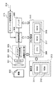
図2は、本発明に係る画像処理装置の一実施形態としての複合機の構成例を示す概略断面図であり、該複合機は機械的構成としてカラースキャナ部Aとプリンタ部Bとから構成されている。なお、ここでは、好ましい実施形態として、電子写真技術を用いたスキャナ付の複合機で説明するが、本発明が対象としている画像データは、ベクトル情報を表す画像信号である。ベクトル情報を表す画像信号とは、PCのような計算機から送られるPDLデータやPDLを解釈することで生成されるプリミティブな中間データは言うまでもなく、スキャナで読み取った画像信号をベクトル化したものなども含まれている。なお、PDLとは、Page Description Languageの略である。これらのベクトル情報は、テキストやグラフィックなどの各種オブジェクトを示すためのデータであり、最終的にビットマップデータに変換されるものである。また、以下の実施形態では、特に電子写真プロセスの複写機やプリンタなどを対象としているが、インクジェットやディスプレイのような他のプロセスを用いた機器でも適用可能である。
<First Embodiment>
FIG. 2 is a schematic cross-sectional view showing a configuration example of a multi-function peripheral as an embodiment of the image processing apparatus according to the present invention. The multi-function peripheral includes a color scanner unit A and a printer unit B as a mechanical configuration. ing. Here, as a preferred embodiment, a multifunction apparatus with a scanner using an electrophotographic technique will be described, but the image data targeted by the present invention is an image signal representing vector information. An image signal representing vector information is not only PDL data sent from a computer such as a PC, but also primitive intermediate data generated by interpreting PDL, as well as a vectorized image signal read by a scanner. include. Note that PDL is an abbreviation for Page Description Language. These vector information are data for indicating various objects such as text and graphics, and are finally converted into bitmap data. In the following embodiments, a copying machine or a printer for an electrophotographic process is particularly targeted. However, the present invention can also be applied to a device using another process such as an ink jet or a display.
図2に示すカラースキャナ部Aにおいて、原稿給送装置201Aは、原稿を最終頁から順に1枚ずつプラテンガラス202A上へ給送する。そして、原稿の読み取り動作終了後、プラテンガラス202A上の原稿を排出するものである。原稿がプラテンガラス202A上に搬送されると、ランプ203Aを点灯し、このランプ203Aを搭載したスキャナユニット204Aを移動させて原稿を露光走査する。この走査による原稿からの反射光は、ミラー205A,206A,207Aおよびレンズ208AによってCCDカラーイメージセンサ(以下、単に「CCD」という)209Aへ導かれる。
In the color scanner section A shown in FIG. 2, the
そして、CCD209Aに入射した反射光は、R,G,Bの3色に色分解され色毎の輝度信号として読み取られる。さらに、CCD209Aから出力される輝度信号はA/D変換によってデジタル信号の画像データとして画像処理部(図3の304参照)に入力される。そして、シェーディング補正、階調補正、量子化(N値化)、スムージング処理などの周知の画像処理が施された後、プリンタ部B(305)へ転送される。
The reflected light incident on the
図2に示すプリンタ部Bにおいて、レーザドライバ221Bは、レーザ発光部201Bを駆動するものであり、画像処理部304から出力された色毎の画像データに応じたレーザ光をレーザ発光部201Bによって発光させる。このレーザ光は感光ドラム202Bに照射され、感光ドラム202Bにはレーザ光に応じた潜像が形成される。
In the printer unit B shown in FIG. 2, the
そして、この感光ドラム202Bの潜像の部分には現像器203Bによって現像剤であるトナーが付着される。なお、図2では、現像器は、図示の簡略化のため、唯一つのみが示されているが、C,M,Y,Kの色毎にトナーが用意され、それに応じて4つの現像器が設けられることは、勿論である。また、以上の構成の代わりに感光ドラムや現像器等を色毎に4組設ける構成であってもよい。
Then, a toner as a developer is attached to the latent image portion of the
上述のレーザ光の照射開始と同期したタイミングで、カセット204Bまたはカセット205Bの選択されたいずれかから記録紙が給紙され、転写部206Bへ搬送される。
The recording paper is fed from either the
これにより、感光ドラム202Bに付着した現像剤を記録紙に転写することができる。現像剤が転写された記録紙は、定着部207Bに搬送され、定着部207Bの熱と圧力により現像剤の記録紙への定着が行われる。そして、定着部207Bを通過した記録紙は排出ローラ208Bによって排出され、ソータ220Bはこの排出された記録紙をそれぞれ所定のビンに収納して記録紙の仕分けを行う。
Thereby, the developer attached to the
なお、ソータ220Bは、仕分けが設定されていない場合は、最上位のビンに記録紙を収納する。また、両面記録が設定されている場合は、排出ローラ208Bのところまで記録紙を搬送した後、排出ローラ208Bの回転方向を逆転させ、フラッパ209Bによって再給紙搬送路へ導く。多重記録が設定されている場合は、記録紙を排出ローラ208Bまで搬送しないようにフラッパ209Bによって再給紙搬送路210Bへ導く。再給紙搬送路へ導かれた記録紙は上述したタイミングで転写部206Bへ給紙される。
The
なお、色毎の潜像および現像の処理や定着は、上述の記録紙搬送機構を用いて、潜像形成等を4回分繰り返すことによって実現することは周知の通りである。 As is well known, the latent image and development processing and fixing for each color are realized by repeating the latent image formation and the like four times using the recording paper transport mechanism described above.
ところで、314はネットワークケーブルであり、一般的にイーサネット(登録商標)と呼ばれるシステムである。これは、10BaseTや10Base5などの物理的なケーブルを用いてTCP/IPなどのプロトコルにより、接続される各ユニット相互の情報授受やデータの転送を行うことができる。無論、ネットワークケーブルを用いた有線に限定されたものではなく、無線を用いても同様な環境構築ができることは言うまでもない。
Incidentally,
このようなネットワークケーブル314を介し、ホストコンピュータなどから送信されたPDLデータやディスプレイリストなどは、プリンタに設けられたインタフェースとしてのネットワーク信号受信部315で受信される。このネットワーク信号受信部315には、ホストコンピュータから送信されたデータを解釈して、画像を示す画素単位のビットマップデータを生成するラスタライズ部(不図示)が含まれている。また、PDLデータまたはディスプレイリストは、テキスト(文字)、フラフィック、イメージ等といったオブジェクト毎にその属性を示すデータを保持している。ラスタライズ部では、この属性データを利用して画像データをセ氏英するとともに、各画素の像域信号も生成する。像域信号については後に詳細に説明する。
PDL data, a display list, and the like transmitted from the host computer or the like via such a
そして、ラスタライズ部で生成された画像データは、画像読み取り部309から入力されたデータと同様に、画像処理部304に入力され、矢印で示したように、フィルタ処理部1604に入力され、必要な画像処理が実行される。また、像域信号はスムージング処理部1605に入力される。カラー画像データの場合、CMYKの色毎の濃度データが生成され、色毎のデータ夫々に対して後段の処理が実行される。
Then, the image data generated by the rasterizing unit is input to the
なお、ラスタライズ部はネットワーク信号受信部315の外部に設けられるものであってもよい。本実施形態では、この314を介して受信したデータを処理する構成について後述する。
Note that the rasterizing unit may be provided outside the network
図3は、図2に含まれる画像処理装置のデータ処理構成を説明するブロック図であり、図2と同一のものには同一の符号を付してある。 FIG. 3 is a block diagram illustrating the data processing configuration of the image processing apparatus included in FIG. 2, and the same components as those in FIG. 2 are denoted by the same reference numerals.
図3において、画像読み取り部309は、レンズ301、CCDセンサー302、アナログ信号処理部303等により構成される。そして、レンズ301を介してCCDセンサー302に結像された原稿画像300が、CCDセンサー302によりアナログ電気信号に変換される。変換された画像情報は、アナログ信号処理部303に入力され、サンプル&ホールド、ダークレベルの補正等が行われた後にアナログ・デジタル変換(A/D変換)される。
In FIG. 3, the
このようにして変換されたデジタル信号は、図4に詳細に示す画像処理部304において、シェーディング補正401、色補正処理402、フィルタ処理403、γ補正処理404、画像形成処理405、スムージング処理406などが各部で行なわれる。その後、プリンタ305へ出力される。この画像形成処理405とは、入力される1画素あたりNビットの画像データを1画素あたりMビットの画像へと変換する処理を行う。具体的には、本実施の形態ではNを8、Mを4とした。画像形成処理の詳細については、公知な処理である為説明は略するが、スクリーン(ディザ)処理や誤差拡散処理などを指している。
The digital signal thus converted is subjected to
本願発明のポイントを含むスムージング処理406以外の処理についても、同様に周知なものであるため、説明を略する。
Since processes other than the smoothing
ところで、図4において、ネットワーク信号受信部315からの信号が色補正処理402の後ろに接続されているが、これは、ネットワークを介して受信した信号がCMYKの濃度データであることを想定している為である。もし、受信した信号がRGBの輝度信号であった場合は、不図示であるが色補正処理402の前に接続されるようになることも言うまでもない。さらに、ネットワークを介して受信した信号がPDL信号の場合は、ネットワーク信号受信部315でビットマップ信号に変換した後、画像処理部304に入力されることは言うまでもない。これら処理は、正確にはネットワークを介して受信した信号はCPU310を介しているのだが、ここでは、信号の流れが分かりやすいように簡略して図4のように示してある。
In FIG. 4, the signal from the network
一方、図3に示すプリンタ305は、レーザ等からなる露光制御部(図示せず)、画像形成部(図示せず)、転写紙の搬送制御部(図示せず)等により構成され、入力された画像信号を転写紙上に記録する。
On the other hand, the
また、CPU回路部310は、CPU306、ROM307、RAM308等により構成され、画像読み取り部309、画像処理部304、プリンタ部305、操作部313等を制御し、複合機のシーケンスを統括的に制御する。
The
操作部313には、RAM311、ROM312が予め用意されており、UI上に文字を表示したり、ユーザが設定した情報を記憶したり、表示したりすることが可能な構成となっている。
The
ユーザによって操作部313で設定された情報は、CPU回路部310を介して、画像読み取り部309、画像処理部304、プリンタ305などに送られる構成となっている。
Information set by the
以上説明した流れの中で、本願発明のポイントは、画像処理部304に含まれている。以下、画像処理部内のスムージング処理部406について説明を行う。尚、以下の各構成要素については、ソフトウエアで実現したものとし、C言語で作成されたプログラムで示すが、これらは等価な機能をハードウエアやファームウエアで構築してもよい。つまり、各構成要素それぞれまたはいくつかの構成要素がASICなどの専用ハードウエアを用いて構成されていても、ソフトウエアによって得られる効果と同様の効果を得ることができる。
In the flow described above, the point of the present invention is included in the
図5は、図4に示したスムージング処理部406の構成を説明する概略ブロック図であり、図4と同一のものには同一の符号を付してある。
FIG. 5 is a schematic block diagram for explaining the configuration of the smoothing
図5においては、1色(ImageData)に対する処理しか示していないが、図4に示したように本処理には4色分のデータが入力されている。つまり、CMYK各色、独立に処理する構成となっており、その内の1色に対する処理を図示している。 In FIG. 5, only processing for one color (ImageData) is shown, but as shown in FIG. 4, data for four colors is input to this processing. In other words, each CMYK color is processed independently, and processing for one of the colors is shown.
まず、はじめに本願発明のポイントであるスムージング処理部406の概略動作フローについて図5を用いて説明する。
First, a schematic operation flow of the smoothing
スムージング処理部406には、画像形成処理(例えばスクリーン処理などの擬似中間調処理)される前の信号であるN=8bitの上位3bitと、各画素の属性を示す像域信号4bitと、画像形成処理された信号であるM=4bitとが入力される。ここでは、画像形成処理前の信号をImageData(第1の画像データ)、像域信号をAttributeData(属性データ)、画像形成処理後の信号をScreenData(InDataS)(第2の画像データ)で表している。
The smoothing
像域信号(AttributeData)とは、各画素がテキスト(文字)、イメージ(写真)、グラフィックなどの画像属性のうち、どの属性に相当する画像を構成する画素であるかを示すデータである。この信号は4bitであり、後述するように属性復号部(Attribute Decoder)510により、8bitの像域信号に変換される。
The image area signal (AttributeData) is data indicating which attribute corresponds to which attribute among the image attributes such as text (character), image (photo), and graphic. This signal is 4 bits, and is converted into an 8-bit image area signal by an
判定手段としての判別部(make_ZSG_sig)501では、スムージング処理を行うか否かの判断の元となる判別信号(OutDataZ)が生成される。そして、エッジ補正生成手段としての処理実行部(make_AST_sig)502で判別信号に応じたスムージング処理を行った後、その出力を選択手段としてのセレクタ(selector)503でScreenDataと比較する。そして、判別信号に応じたスムージング処理がされた画素データ値と、ScreenDataの値のうち、画素値が高い方のデータを出力データ(OutputData)として出力する構成となっている。
A determination unit (make_ZSG_sig) 501 serving as a determination unit generates a determination signal (OutDataZ) that is a basis for determining whether to perform smoothing processing. Then, after a smoothing process corresponding to the discrimination signal is performed by a process execution unit (make_AST_sig) 502 as an edge correction generation unit, the output is compared with ScreenData by a
以下、上述したスムージング処理部406の各部における処理について詳細に説明する。
Hereinafter, the process in each part of the
図6は、図5に示した属性復号部(Attribute Decoder)510で行なわれる処理を説明する図である。図6の(a)において601(Attribute Decoder input)で示した部分が、属性復号部に入力される属性データ(AttributeData)である。この入力信号601の各ビットは、ラインの太さやオブジェクトの有無や文字/非文字やベクタ/非ベクタなどの属性を示している。例えば、bit4が線や文字の太さを示すフラグ、bit5がオブジェクトの有無を示すフラグ、bit2が文字/非文字を示すフラグ、bit0がベクタ/非ベクタを示すフラグなどである。4つのビットがbit0〜bit3まで順に並んでいない理由は、4ビット以上ある信号の中から任意に選択したものである為である。
FIG. 6 is a diagram for explaining processing performed by the
これらの信号をもとに、属性復号部(Attribute Decoder)510では8bitの信号を生成している。本実施の形態で生成した信号の詳細は、図6の(b)のテーブルに示した通りであるが、ポイントだけ書き出すと以下のようになる。
Based on these signals, an
ImageType0:00000001(0x01):未使用
ImageType1:00000010(0x02):未使用
ImageType2:00000100(0x04):グラフィック
ImageType3:00001000(0x08):線
ImageType4:00010000(0x10):文字
ImageType5:00100000(0x20):小さいグラフィック
ImageType6:01000000(0x40):細い線
ImageType7:10000000(0x80):小さい文字
ここで、(b)のテーブルにおいてREOSという文字は、ラインや文字が細い/小さいという意味を表している。この細い/小さいについては、PDLなどの画像データを生成し、プリンタに送信するホストコンピュータに設けられたプリンタドライバで既に行なわれた判別結果を示している。プリンタドライバの設定次第で細い/小さいと判別される閾値は任意であることは言うまでもない。また、ネットワーク信号受信部315において判別する構成であってもよい。
ImageType0: 00000001 (0x01): Not used
ImageType1: 00000010 (0x02): Not used
ImageType2: 00000100 (0x04): Graphic
ImageType3: 00001000 (0x08): Line
ImageType4: 00010000 (0x10): Character
ImageType5: 00100000 (0x20): Small graphic
ImageType6: 01000000 (0x40): Thin line
ImageType7: 10000000 (0x80): small character Here, the character REOS in the table of (b) means that the line and the character are thin / small. This thin / small indicates the determination result already made by the printer driver provided in the host computer that generates image data such as PDL and transmits it to the printer. It goes without saying that the threshold value determined to be thin / small is arbitrary depending on the setting of the printer driver. Further, the network
以上説明したように、属性復号部(AttributeDecoder)510は、4bitの入力を8bit出力に変換するテーブル変換メモリで構成されている。 As described above, the attribute decoding unit (AttributeDecoder) 510 includes a table conversion memory that converts a 4-bit input into an 8-bit output.
次に、判別部(make_ZSG_sig)501の動作について、図7A〜7Cを参照して説明する。図7Aは入出力される信号を示すブロック図であり、図7B及び7Cは判別部501での処理をプログラム言語(C言語)で記載した例を示している。
Next, the operation of the determination unit (make_ZSG_sig) 501 will be described with reference to FIGS. FIG. 7A is a block diagram showing input / output signals, and FIGS. 7B and 7C show examples in which the processing in the
図7Aに示すように、本実施形態の判別部501には、前述した属性復号部(AttribureDecoder)510(なお、図7Bのプログラム中にはattrdecと記載)から出力された8bitの信号(AttributeDec.Sig.)と、画像形成処理前の信号であるImageDataの上位3bitの信号InData(=InData')に応じて、図7Bに示すような処理によって判別信号(OutDataZ)を生成している。なお、reg_atbとは、モードセレクタ(レジスタ)である。
As shown in FIG. 7A, the
InData信号については、図7BのAで示す部分において、任意の数値(レジスタ:reg_Zcheck)と比較して、大小関係に応じて判別信号(OutDataZ)を制御する処理を行っている。また、AttibuteDecoder信号については、図7BのBで示す部分において、任意のオブジェクトに応じて、判別信号(OutDataZ)を制御する処理を行っている。図7BにおいてThinJudgeはレジスタであり、これより、任意の濃度以上でかつ任意のオブジェクトに対してのみスムージング処理をかけるように制御することが可能となっている。例えば、一定値以上の文字のみに対してスムージング処理を行うなどの制御を可能とするものである。 With respect to the InData signal, in the part indicated by A in FIG. 7B, processing for controlling the determination signal (OutDataZ) according to the magnitude relationship is performed in comparison with an arbitrary numerical value (register: reg_Zcheck). In addition, for the AttibuteDecoder signal, processing for controlling the discrimination signal (OutDataZ) is performed in the part indicated by B in FIG. 7B in accordance with an arbitrary object. In FIG. 7B, ThinJudge is a register, and from this, it is possible to perform control so that smoothing processing is performed only on an arbitrary object having an arbitrary density or higher. For example, it is possible to perform control such as performing a smoothing process only on characters having a certain value or more.
ところで、本実施形態の判別部501は、この制御だけに限定したものではなく、他の幾つかの制御も可能な構成としてある。これら制御の切替えは、上述したモードセレクタ(レジスタreg_atb)の信号に応じて行なわれる。
By the way, the
例えば、図7CのCで示した部分において、reg_atb=1の場合は、画像形成前の信号(InData)の大きさだけに応じて、判別信号(OutDataZ)が制御される。言うまでもないが、reg_Zcheck(レジスタ)に応じて任意に制御可能である。 For example, in the part indicated by C in FIG. 7C, when reg_atb = 1, the determination signal (OutDataZ) is controlled only according to the magnitude of the signal (InData) before image formation. Needless to say, it can be arbitrarily controlled according to reg_Zcheck (register).
そして、図7CのDで示した部分において、reg_atb=2の場合は、画像形成処理された信号(InDataS)の大きさだけに応じて、判別信号(OutDataZ)が制御される。これも同様に、reg_air(レジスタ)に応じて任意に制御可能である。 In the portion indicated by D in FIG. 7C, when reg_atb = 2, the determination signal (OutDataZ) is controlled only in accordance with the magnitude of the image-formed signal (InDataS). Similarly, this can be arbitrarily controlled according to reg_air (register).
最後にレジスタreg_atbの値がその他の場合の処理が、図7CのEで示した部分である。これは、出力信号がすべて0になるため、本処理の出力位相(タイミング)を保った状態でスルー出力を実現するために用意されている。 Finally, the processing when the value of the register reg_atb is other is the part indicated by E in FIG. 7C. Since all the output signals are 0, this is prepared for realizing the through output while maintaining the output phase (timing) of this processing.
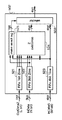
次に、処理実行部(make_AST_sig)502について図1を参照して説明する。なお、図1には、説明の便宜上セレクタ503を含めて示している。この部分は従来例と比較して、コストダウンの効果が一番大きいブロックである。
Next, the process execution unit (make_AST_sig) 502 will be described with reference to FIG. 1 includes the
図1に示したように、処理実行部(make_AST_sig)502には、前述した判別部(make_ZSG_sig)で生成した1bitの判別信号(OutDataZ)と、画像形成処理前の上位3bitの信号(InData)と、画像形成処理後(例えばスクリーン処理などの疑似中間調処理後)の4bitの信号(InDataS)とが入力され、4bitの信号が出力される構成となっている。これら3つの信号それぞれは、図示したようなFiFoメモリ521〜523に入力されており、所定のライン数だけ遅延されるようになっている。本実施形態では、このメモリのサイズを従来と比較して大きく削減している。さらに、従来と同等な効果を維持しつつ、処理系も簡素化している。
As shown in FIG. 1, the processing execution unit (make_AST_sig) 502 includes a 1-bit determination signal (OutDataZ) generated by the above-described determination unit (make_ZSG_sig), and a high-
そして、FiFoメモリ521及び522を介して、判別信号(OutDataZ)と画像形成処理前の上位3bitの信号(InData)とが再生部(Zexistence)524に入力され、エッジ部の信号のみが再生される。そしてセレクタ(selector)503で、選択部(make_select_sig)525の出力に応じて、画像形成処理後の4bitの信号(InDataS)と、再生部(Zexistence)の出力信号とのいずれかが選択されて出力される構成となっている。なお、選択部(make_select_shig)525では、画像形成処理前の上位3bitの信号(InData)と、画像形成処理後の4bitの信号(InDataS)との差(濃度値の差)に応じて選択信号が生成される。本実施形態では処理をこのように簡略化することによって、コストダウンを実現している。具体的な処理については後述する。
Then, the discrimination signal (OutDataZ) and the upper 3 bits signal (InData) before the image forming process are input to the reproduction unit (Zexistence) 524 via the
まず、選択部(make_select_sig)525について図8A及び8Bを参照して説明する。図8Aは選択部525の入出力を示すブロック図であり、図8Bは選択部525での処理をプログラム言語(C言語)で記述した例を示している。
First, the selection unit (make_select_sig) 525 will be described with reference to FIGS. 8A and 8B. FIG. 8A is a block diagram showing input / output of the
選択部525には、前述した通りInDataとInDataSとが入力されている。基本的には、これらの信号の大小関係を比較し、InDataの方が大きければ1を出力し、小さければ0を出力するといった処理を行う。ただし、これらInDataとInDataSとの比較は、3ビットと4ビットの比較となるため、図8Bのプログラム例に示したようなビット揃え処理を行った後に比較を行う。プログラム中では、InDataをsel_InDataに変換し、InDataSをsel_InDataSに変換した後、比較している。
As described above, InData and InDataS are input to the
このように、InDataとInDataSとを比較し、濃度の濃い方、即ちビット値が大きい方の信号を選択する構成にすることによって、エッジが細ったり、濃度が薄くなったりして、全体の画質レベルが下がることを防止できる。 In this way, by comparing InData and InDataS and selecting a signal with a higher density, that is, a signal with a larger bit value, the edge becomes thinner or the density becomes lower, resulting in an overall image quality. You can prevent the level from going down.
つまり、後述する再生部(Zexistence)524で再生したエッジ信号の方が、元のInDataSのエッジ信号より薄かった場合に、再生部の出力信号を出力すると、上述したようにエッジ部が薄くなり、全体の画質レベルが下がる。これを防止するように選択部(make_select_sig)525が設けられている。 That is, when the edge signal reproduced by the reproduction unit (Zexistence) 524 described later is thinner than the original InDataS edge signal, when the output signal of the reproduction unit is output, the edge portion becomes thin as described above. The overall image quality level is lowered. A selection unit (make_select_sig) 525 is provided to prevent this.
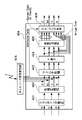
さらに本実施形態の特徴でもある再生部(Zexistence)524での処理を、図9のブロック図を参照して詳細に説明する。 Further, processing in the reproduction unit (Zexistence) 524, which is also a feature of the present embodiment, will be described in detail with reference to the block diagram of FIG.
再生部(Zexistence)524には、3ラインのInDataとOutDataZ、そして、注目ラインのInDataSとが入力されている。そして、内部に3×3のスムージング処理部(x3smooth)5241、パターンマッチング処理部(miniSST)5242、エッジ検出処理部(BorderCount&DensCheck)5243、適応スムージング処理部(AdaptiveSmoothing)5244を有し、各部での処理を行って、4bitの出力信号を生成している。以下、順に各部での処理を説明する。 The reproduction unit (Zexistence) 524 receives three lines of InData and OutDataZ, and an attention line InDataS. It has a 3 × 3 smoothing processing unit (x3smooth) 5241, a pattern matching processing unit (miniSST) 5242, an edge detection processing unit (BorderCount & DensCheck) 5243, and an adaptive smoothing processing unit (AdaptiveSmoothing) 5244. To generate a 4-bit output signal. Hereinafter, the process in each part is demonstrated in order.
まず、3×3スムージング処理部(x3smooth)5241では、InDataに含まれる3×3領域の画素の濃度平均を求めている。濃度平均を求める処理は公知のため、詳細な説明は省略するが、例えば、9画素内にある濃度1の画素(記録画素)の数を求め、9で割るといった演算を行っている。ただし、本実施の形態では、演算処理部の負荷を減らすため、3×3の領域内にある記録画素の数を求めた後、3ビットシフト(=÷8相当)を行って出力信号(smoothData)を得ている。
First, the 3 × 3 smoothing processing unit (x3 smooth) 5241 calculates the average density of the pixels in the 3 × 3 region included in InData. Since the process for obtaining the density average is well known, detailed description is omitted. For example, the number of
次に、パターンマッチング処理部(miniSST)5242では、パターンマッチングにより、プリンタ解像度に依存したジャギーを改善する為のスムージング処理を行っている。プリンタ解像度に依存したジャギーとは、例えば、プリンタの解像度が300dpiなら、フォントやラインのガタツキとして、図14に示したようなL字型の部分が発生する。そこで、図12に示したようなパターンと、InDataを任意の閾値で2値化した信号(不図示)とを3×3の領域でマッチングする。そして、一致した箇所を、図9に示した3×3スムージング処理部(x3smooth)5241の出力信号(smoothData)で置き換える処理を行っている。なお、図12に示したパターンは本実施の形態で用いた一例にすぎず、これに限定したものではないことは言うまでもない。このようにプリンタ解像度に依存したジャギーが改善された3bitの信号(patternCK)が後述する適応スムージング処理部(AdaptiveSmoothing)5244に入力される。 Next, a pattern matching processing unit (miniSST) 5242 performs a smoothing process for improving jaggy depending on the printer resolution by pattern matching. For example, if the printer resolution is 300 dpi, the jaggy depending on the printer resolution generates an L-shaped portion as shown in FIG. Therefore, the pattern as shown in FIG. 12 and a signal (not shown) obtained by binarizing InData with an arbitrary threshold value are matched in a 3 × 3 region. Then, a process of replacing the coincident portion with the output signal (smoothData) of the 3 × 3 smoothing processing unit (x3 smooth) 5241 shown in FIG. 9 is performed. Needless to say, the pattern shown in FIG. 12 is only an example used in the present embodiment, and the present invention is not limited to this. In this way, a 3-bit signal (patternCK) with improved jaggy depending on the printer resolution is input to an adaptive smoothing processing unit (Adaptive Smoothing) 5244 described later.
一方、エッジ検出処理部(BorderCount&DensCheck)5243は、OutDataZ信号を用いてエッジ検出信号を生成している。図10Aはエッジ検出処理部5243の入出力を示しており、図10Bはエッジ検出処理部5243の処理をプログラム言語(C言語)で記述した例を示している。
On the other hand, the edge detection processing unit (BorderCount & DensCheck) 5243 generates an edge detection signal using the OutDataZ signal. 10A shows input / output of the edge
図10Aに示したように、エッジ検出処理部5243には、前述したOutDataZ(=DataZ)信号3ラインと、InData信号1ライン(注目ライン)とが入力され、エッジ検出信号bc(=out)を生成している。具体的には、まず、図10BにおいてAで示した部分で、OutDataZ(=DataZ)の1bit信号を用いて3×3の領域内の濃度1の画素(記録画素)の数をカウントする(sum=bc)。3×3の領域なので合計9が最大になる。つまり、4bit信号である。なお、図10Bのプログラム中にvalCheck()で示された関数は、画像の端部判定をしているだけであり、本質的な処理ではないためここでの説明は省略する。そして、上述したsum=bcを図10BのBで示す部分で、再処理して最終的な4bit信号bcを生成して出力する構成となっている。
As shown in FIG. 10A, the edge
ここでは、任意のレジスタ(reg_Zcheck)に格納された濃度値とInData(=data)に含まれる画素の濃度値が近くて、かつInData(=data)が0ならば、前述のようにして求めたsumの値をクリアする(値をゼロに置換する)処理を行っている。これにより、グラデーションなどのような濃度が徐々に変化する領域において、誤ったエッジ信号により階調が不連続となるのを改善できる。つまり、図7Bで説明したInDataの濃度と属性復号部の出力信号とから図7BのAで示す処理を実行すると、グラデーションの途中で出力信号(OutDataZ)を1としてしまう場合が生じる為、それをクリアする処理をここで行っている。 Here, if the density value stored in an arbitrary register (reg_Zcheck) is close to the density value of the pixel included in InData (= data) and InData (= data) is 0, it is obtained as described above. Processing to clear sum value (replace value with zero) is performed. As a result, in a region where the density gradually changes, such as gradation, it is possible to improve that the gradation becomes discontinuous due to an erroneous edge signal. That is, when the process indicated by A in FIG. 7B is executed from the InData density and the output signal of the attribute decoding unit described in FIG. 7B, the output signal (OutDataZ) may be set to 1 in the middle of the gradation. The clearing process is performed here.
最後に、適応スムージング処理部(AdaptiveSmoothing)5244の詳細について、図11A及び図11Bを参照して説明する。図11Aは適応スムージング処理部5244の入出力を示しており、図11Bは適応スムージング処理部5244の処理をプログラム言語(C言語)で記述した例を示している。
Finally, details of the adaptive smoothing processing unit (AdaptiveSmoothing) 5244 will be described with reference to FIGS. 11A and 11B. 11A shows input / output of the adaptive
適応スムージング処理部5244には、入力信号として前述したPatternCKとInDataとInDataSとbcとが入力され、4bitの信号が出力される構成となっている。具体的には、条件「(bc==0 || bc>=astPower)かつ(InData!=0)」を満たす場合に、画像形成された信号InDataSをスルー出力する。それ以外の場合には、条件「ast_params->sstAllOffSW==0(レジスタ)」を満たすときに、InDataSをLUTEというテーブルを介して出力する。上記2つの条件のいずれも満たさない場合には、LUTEというテーブルを介してpatternCKを出力する構成となっている。
The adaptive
ここで、LUTEはメモリで構成されたルックアップテーブルであり、3bit入力4bit出力のメモリ空間を有したものであるが、基本的には、リニアな出力変換を行うように設定されている。ただし、プリンタの記録特性に応じて、非線形な出力となるように設定してもよいのはもちろんである。また、エッジ部の出力ビット数を4bit以外にしたいときも、このテーブルを用いて変換可能である。 Here, LUTE is a look-up table configured by a memory, and has a memory space of 3 bits input and 4 bits output, but is basically set to perform linear output conversion. However, it is of course possible to set the output to be nonlinear according to the recording characteristics of the printer. Also, when it is desired to change the number of output bits of the edge portion to other than 4 bits, conversion is possible using this table.
ところで、上述した第2の条件式の「astPower」は、レジスタであり、本実施形態では、この値に応じて、エッジ再処理信号への置き換え幅を調整可能であることも特徴としている。実際にエッジ再処理信号の置き換え幅を変えた画像の例を図13に示した。astPowerの値を小さくした場合(lebel1)を(a)に示し、astPowerの値が大きくなるにつれて、(b)(level2)、(c)(level3)に示すようになる。このときの画像データは、(a)→(b)→(c)でエッジ部のハーフトーン画素数が増えている。この画素数が増すと、エッジ部の滑らかさも増すことになる。このパラメータは、ハーフトーン画素の追加によって文字が縁取られたような画像にならない程度に調整して用いられる。
本機能は、従来手法にはなかったものであり、これにより一層高機能な処理を実現している。
Incidentally, “astPower” in the second conditional expression described above is a register, and this embodiment is also characterized in that the replacement width to the edge reprocessing signal can be adjusted according to this value. An example of an image in which the replacement width of the edge reprocessed signal is actually changed is shown in FIG. When the value of astPower is reduced (lebel1) is shown in (a), and as the value of astPower is increased, it becomes as shown in (b) (level2), (c) (level3). In the image data at this time, the number of halftone pixels in the edge portion increases from (a) → (b) → (c). As the number of pixels increases, the smoothness of the edge portion also increases. This parameter is used after being adjusted to such an extent that the image does not appear as if the character is trimmed by the addition of halftone pixels.
This function is not present in the conventional method, and thereby realizes more sophisticated processing.
一方、上記の第2の条件式における「ast_params->sstAllOffSW」もレジスタであり、上述のように0に設定されている場合は、LUTEを介してInDataが出力される構成となっている。つまり、前述したパターンマッチング処理部(miniSST)5242での処理結果を反映しないスムージングも行える構成となっている。パターンマッチング処理部5242での処理を反映しないということは、プリンタ解像度より高い解像度では、スムージング処理を行わないということである。
On the other hand, “ast_params-> sstAllOffSW” in the second conditional expression is also a register, and when it is set to 0 as described above, InData is output via LUTE. That is, smoothing that does not reflect the processing result in the pattern matching processing unit (miniSST) 5242 described above can be performed. Not reflecting the process in the pattern
以上説明した各部での処理を施した結果が、図1で示した再生部(Zexistence)524から出力され、セレクタ(selector)503で、選択部(make_select_shig)525の出力に応じて、画素毎に画像形成処理後の4bitの信号(InDataS)と、再生部(Zexistence)の出力信号とのいずれかが選択されて、スムージング処理406の結果としてプリンタ305に出力される。出力されるイメージは、前述した図13のとおりである。
The result of performing the processing in each unit described above is output from the reproduction unit (Zexistence) 524 shown in FIG. 1, and the selector (selector) 503 outputs each pixel in accordance with the output of the selection unit (make_select_shig) 525. Either the 4-bit signal (InDataS) after the image forming process or the output signal of the reproduction unit (Zexistence) is selected and output to the
図13は、本実施形態の画像処理装置におけるエッジ処理結果を示す図であり、着目箇所は、エッジ部である。図13に示したようにスクリーンのパターンの間を埋めるようにデータが薄く、かつ、可変な幅で出力されることを特徴としている。本実施形態の構成により、この処理を従来と比較してローコストにかつ高機能に実現できる。 FIG. 13 is a diagram illustrating an edge processing result in the image processing apparatus according to the present embodiment, and a point of interest is an edge portion. As shown in FIG. 13, the data is thin and is output with a variable width so as to fill the space between the screen patterns. With the configuration of the present embodiment, this process can be realized at a lower cost and with higher functionality than in the prior art.
不図示だが、さらに、JPEGのような非可逆な圧縮処理を施した画像に対しても、問題なくエッジ部の改善ができるという特徴も有している。 Although not shown, there is also a feature that the edge portion can be improved without problems even for an image subjected to irreversible compression processing such as JPEG.
その理由は、エッジ検出用のデータを作成する際、8ビット画像データの上位側3ビット信号より1ビットの像域信号を作成しているため、圧縮による微妙な劣化情報を除去できるという効果が得られるためである。 The reason is that, when creating edge detection data, a 1-bit image area signal is created from the upper 3-bit signal of 8-bit image data, so that it is possible to remove subtle deterioration information due to compression. It is because it is obtained.
以上説明したように、本実施形態によれば、プリンタの解像度によるジャギーはもちろんのこと、175線や133線等のスクリーンを用いた疑似中間調処理によってエッジ部に発生するジャギーをも改善することが可能となる。このようなスクリーンのジャギーは、プリンタの解像度より遥かに低い解像度で発生するため、ハーフトーン文字やラインで顕著に目立っていたが、これを改善することが可能である。 As described above, according to the present embodiment, not only jaggy due to the resolution of the printer but also the jaggy generated at the edge portion by the pseudo halftone process using a screen such as 175 line or 133 line is improved. Is possible. Since such screen jaggies occur at a resolution much lower than the resolution of the printer, it was conspicuous in halftone characters and lines, but this can be improved.
さらに、エッジ再処理信号への置き換え幅を調整可能にすることで、よりラチチュードの高い処理を実現した。置き換え幅の調整により、図13に示した効果が得られる。これによって、様々なプリンタ特性に対応できるようになった。 Furthermore, processing with higher latitude was realized by making it possible to adjust the width of replacement with edge reprocessed signals. The effect shown in FIG. 13 can be obtained by adjusting the replacement width. As a result, various printer characteristics can be accommodated.
さらに、本実施形態を用いると、スキャナで読み込んだイメージ画像をベクトル化したものにも容易に対応可能である。なお、ベクトル化とは、ビットマップデータをアウトラインデータに変換することを意味する。 Furthermore, when this embodiment is used, it is possible to easily cope with a vectorized image read by a scanner. Note that vectorization means converting bitmap data into outline data.
<第2の実施形態>
以下、本発明に係る画像処理装置の第2の実施形態について説明する。以下の説明では、上記第1の実施形態と同様な部分については説明を省略し、第2の実施形態の特徴的な部分を中心に説明する。
<Second Embodiment>
Hereinafter, a second embodiment of the image processing apparatus according to the present invention will be described. In the following description, description of parts similar to those of the first embodiment will be omitted, and description will be made focusing on characteristic parts of the second embodiment.
上記第1の実施形態は、入力画像信号の解像度が600dpiであったのに対し、本実施形態では入力解像度信号が1200dpi及び600dpiの両方の解像度に対応できる構成となっている。 In the first embodiment, the resolution of the input image signal is 600 dpi, whereas in the present embodiment, the input resolution signal is configured to support both 1200 dpi and 600 dpi resolution.
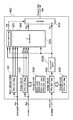
図17は、本願発明のポイントであるスムージング処理部406’の構成を説明する概略ブロック図であり、第1の実施形態に関して説明した図5に対応しており、同様な部分を同じ参照符号で示している。
FIG. 17 is a schematic block diagram illustrating the configuration of the smoothing
図17に示したスムージング処理部406’を図5のスムージング処理部406と比較する。すると、1200dpiに対応するために、1701で示すビットマスク部(ScreenBitMask)と1702で示すビット変換部(bit32_conv)が追加となっている。また、後述するように処理実行部(make_AST_sig)502’も1200dpiに対応するために変更されている。
The smoothing processing unit 406 'shown in FIG. 17 is compared with the smoothing
これらブロックの追加および変更により、第1の実施形態と同様な基本構成で、1200dpiへの対応を実現した。このように本実施形態は、600dpiと1200dpiとの両方の解像度に同一のハード構成で対応可能とした点を特徴とする。 By adding and changing these blocks, 1200 dpi is realized with the same basic configuration as in the first embodiment. As described above, the present embodiment is characterized in that both the resolutions of 600 dpi and 1200 dpi can be handled with the same hardware configuration.
以下、第1の実施形態に関して説明した図5の構成と異なる各ブロックについて詳細に説明する。 Hereinafter, each block different from the configuration of FIG. 5 described in regard to the first embodiment will be described in detail.
図18Aはビットマスク部(ScreenBitMask)1701の入出力信号を示すブロック図であり、図18Bはビットマスク部1701での処理をプログラム言語(C言語)で記載した例を示している。
FIG. 18A is a block diagram showing input / output signals of the bit mask unit (ScreenBitMask) 1701, and FIG. 18B shows an example in which processing in the
図18Bにおいて、「ast_params->bit_select」で示されのはパラメータであり、処理解像度が1200dpiであるか600dpiであるかに応じて、2/3あるいは0/1が選択される構成となっている。 In FIG. 18B, “ast_params-> bit_select” indicates a parameter, and 2/3 or 0/1 is selected depending on whether the processing resolution is 1200 dpi or 600 dpi. .
これは、後述するFiFoメモリの容量を削減するために、1200dpiモードの際に上位ビットのみを使用して下位ビットをマスクするような構成となっているためである。ただし、ハード構成上の関係で、各ブロックを接続する信号線のビット数は600dpiのビット数(4bit)に合わせてある。そのため、1200dpiの処理時も出力ビット数を4bitと記載してある。繰り返しになるが、1200dpiの処理時はFiFoメモリに格納するための有効データ量を削減するようにビットマスク部は構成されている。 This is because the lower bits are masked using only the upper bits in the 1200 dpi mode in order to reduce the capacity of the FiFo memory described later. However, because of the hardware configuration, the number of bits of the signal line connecting each block is adjusted to the number of bits (4 bits) of 600 dpi. For this reason, the number of output bits is also described as 4 bits even during 1200 dpi processing. Again, the bit mask unit is configured to reduce the amount of effective data to be stored in the FiFo memory during 1200 dpi processing.
なお、第1の実施形態において述べたのと同様に、本ブロックへ入力される信号は、スクリーニング処理或いは誤差拡散処理などによって量子化されたものである。 As described in the first embodiment, a signal input to this block is quantized by a screening process or an error diffusion process.
次に、ビット変換部(bit32_conv)1702について、図19Aの入出力信号を示すブロック図、及び図19Bのビット変換部1702での処理をプログラム言語(C言語)で記載した例を参照して説明する。
Next, the bit conversion unit (bit32_conv) 1702 will be described with reference to a block diagram showing input / output signals in FIG. 19A and an example in which processing in the
図19Bにおいて、「ast_params->dpi_select」で示されるパラメータは、1200dpi出力時のときのみ1に設定される構成となっている。 In FIG. 19B, the parameter indicated by “ast_params-> dpi_select” is set to 1 only when 1200 dpi is output.
600dpi処理と共通ブロックになっているため、図19Aに示すように入出力のビット数が3bitになっている。しかし、1200dpi処理時には図19Bに示すように、パラメータast_params->bit32_conv1〜7に設定された値が出力され、2bit化されることになる。2bit化された信号は、上詰めされた状態で出力される構成となっている。そして出力された信号は、後述する処理実行部(make_AST_sig)502’に入力され、FiFoメモリに格納される。 Since it is a common block with 600 dpi processing, the number of input / output bits is 3 bits as shown in FIG. 19A. However, at the time of 1200 dpi processing, as shown in FIG. 19B, the value set in the parameter ast_params-> bit32_conv1-7 is output and converted into 2 bits. The 2-bit signal is output in a packed state. The output signal is input to a process execution unit (make_AST_sig) 502 'described later and stored in the FiFo memory.
図20は、本実施形態の処理実行部(make_AST_sig)502’の構成を示すブロック図である。図1に示した第1の実施形態の処理実行部502と比較すると、本実施形態の処理実行部502’には、FiFoメモリを用いてデータを遅延させるブロックが含まれている。以下、この遅延について説明する。
FIG. 20 is a block diagram illustrating a configuration of the processing execution unit (make_AST_sig) 502 ′ according to the present embodiment. Compared to the
まず、判別信号(OutDataZ)については、1200/600dpiの解像度に依存せず、第1の実施形態と同様にFiFoメモリ521によって1bitの信号を2ライン遅延させる構成となっている。よって、1200dpi処理を行ってもメモリ容量は増加しない。
First, the discrimination signal (OutDataZ) does not depend on the resolution of 1200/600 dpi, and is configured to delay the 1-bit signal by two lines by the
一方、画像形成処理後の4bitの信号InDataSについては、600dpiでの処理時は4bit1ラインを遅延させ、1200dpiでの処理時は2bit1ラインを遅延させる構成となっている。すなわち、1つのFiFoメモリを、600dpiでの処理時は4bit1ラインを遅延させるメモリ523として用い、1200dpiでの処理時は2bit1ラインを遅延させるメモリ523’として用いる。このように、1200dpiでの処理時にはメモリの長さ方向(幅)が2倍になってしまうが深さ方向(高さ)のbit数を半分にすることで、トータルのメモリ容量が同じとなるようにしてある。これにより、InDataSに関しては、1200dpiでの処理を可能としつつトータルのメモリ容量を増大させる必要が無い。
On the other hand, the 4-bit signal InDataS after the image forming process is configured to delay the 4-
言うまでもないが、1200dpiの1ビット信号が本ブロックに入力されるのは、図18A及び図18Bに関して説明したように、ビットマスク部(ScreenBitMask)1701でパラメータast_params->bit_selectが3に設定された場合である。 Needless to say, a 1200-bit 1-bit signal is input to this block when the parameter ast_params-> bit_select is set to 3 in the bit mask part (ScreenBitMask) 1701, as described with reference to FIGS. 18A and 18B. It is.
次に、画像形成処理前の3bitの信号InDataにかかるFiFoメモリ522’について説明する。600dpiでの処理時は、図に記載したように3bit信号を2ライン遅延させる構成となっている。しかし、1200dpiでの処理時は、図21に関して後述するように、入出力変換部2001によってFiFoメモリの前後でビット変換が行われるように構成されている。
Next, the FiFo memory 522 'related to the 3-bit signal InData before the image forming process will be described. When processing at 600 dpi, the 3 bit signal is delayed by two lines as shown in the figure. However, when processing at 1200 dpi, as will be described later with reference to FIG. 21, the input /
図21A〜21Cを参照して、入出力変換部2001による1200dpiでの処理について説明する。図21Aは入出力変換部2001の構成をFiFoメモリ522’と共に示すブロック図である。
With reference to FIGS. 21A to 21C, processing at 1200 dpi by the input /
まず、入力変換部(bit21_conv)2101によってInDataから1bit信号と2bit信号とが生成される。図21Bは入力変換部2101に含まれるbit21_convモジュールでの処理をプログラム言語(C言語)で記載した例を示している。この1bitと2bitの信号は、1ライン遅延された2bit信号と、さらに1ライン遅延された1bit信号とからなることを特徴としている。つまり、注目画素から離れるとビット精度が落ちる構成となっている。その状態でFiFoメモリ522’に入力することにより、メモリ容量を600dpi処理時から増大させないようにしている。
First, the input conversion unit (bit21_conv) 2101 generates a 1-bit signal and a 2-bit signal from InData. FIG. 21B shows an example in which processing in the bit21_conv module included in the
一方、FiFoメモリ522’からの読み出し時は、bit21_convと、bit23_convとの2つのモジュールを含む出力変換部2102によって、3bit信号に変換される。bit21_convモジュールでの処理は図21B、bit23_convモジュールでの処理は図21Cにそれぞれプログラム言語(C言語)で記載された例に示される通りである。これらの出力時の変換のポイントをまとめると、前述したパラメータast_params->dpi_selectが1、すなわち、1200dpiが指定された場合、ast_params->bit21_convやast_params->bit23_conv1〜3のパラメータに従い、各ライン遅延のデータを3bit信号に変換(置換)する構成となっている。
On the other hand, when reading from the FiFo memory 522 ', it is converted into a 3-bit signal by the
最後に、FiFoメモリ523又は523’からの出力された信号をビットシフトするビットシフト部(ScreenBitShift)2002について、図22Aの入出力信号を示すブロック図、及び図22Bの処理をプログラム言語(C言語)で記載した例を参照して説明する。
Finally, with respect to the bit shift unit (ScreenBitShift) 2002 that bit-shifts the signal output from the
ビットシフト部2002での処理の詳細は図22Bに記載した通りであり、詳しい説明は省略する。しかし、ポイントとしては、入力されたInDataSのビット数が異なっても、第1の実施形態で説明した600dpi用のハード構成が共通で使えるようにビット数を4bitにそろえるようにビットシフトを行っている。
Details of the processing in the
以上説明したように、本実施形態によれば、600dpiでの処理を行う第1の実施形態と同様なハード構成で、かつ、同一容量のFiFoメモリを用いて、1200dpiでの処理を行うことができる。つまり、本実施形態によれば、コストアップすることなく600dpi及び1200dpiの両方での処理が実現可能である。 As described above, according to the present embodiment, 1200 dpi processing can be performed using the same hardware configuration as the first embodiment that performs processing at 600 dpi and the same capacity of the FiFo memory. it can. That is, according to the present embodiment, processing at both 600 dpi and 1200 dpi can be realized without increasing costs.
<その他の実施の形態>
以上説明したように本発明は、画像形成処理後のデータを使用しているため、画像形成処理に忠実な補正ができることを特徴としている。つまり、Faxのような解像度の低いプリンタにも適しているといえる。ただし、従来の手法と異なり、本発明によれば、JPEGのような非可逆圧縮法を施した画像に対しても、エッジ部の画質劣化を補うような出力が可能となるという効果が得られる。
<Other embodiments>
As described above, the present invention uses the data after the image forming process, and is characterized in that correction faithful to the image forming process can be performed. In other words, it can also be said to be suitable for a printer with a low resolution such as Fax. However, unlike the conventional method, according to the present invention, it is possible to output an image that has been subjected to an irreversible compression method such as JPEG so as to compensate for image quality degradation at the edge portion. .
また、スクリーン処理のような画像形成処理だけでなく、誤差拡散系の画像形成処理を施した画像に対しても効果がある。誤差拡散系処理を施したハーフトーン文字やラインは、ジャギーとは異なるガタツキがあるが、それをも改善可能とした。 Further, it is effective not only for image forming processing such as screen processing, but also for images subjected to error diffusion type image forming processing. Halftone characters and lines that have been subjected to error diffusion processing have a backlash that is different from jaggies, but this can also be improved.
さらに、JPEGのような非可逆な圧縮を施すことにより発生するエッジ部のモスキートノイズに対しても効果がある。つまり、圧縮により発生したエッジ部の劣化を本発明では改善可能である。 Furthermore, it is also effective against mosquito noise at the edge portion that is generated by irreversible compression such as JPEG. That is, the degradation of the edge portion caused by the compression can be improved in the present invention.
本発明は、複数の機器から構成されるシステムに適用しても良いし、また、一つの機器からなる装置に適用しても良い。 The present invention may be applied to a system composed of a plurality of devices, or may be applied to an apparatus composed of a single device.
例えば、本発明を画像処理装置に適用すると、スキャナで読み込んだイメージ画像、コンピュータ機器から送信したPDL画像の両方におけるエッジ部の画質を改善することが可能となる。 For example, when the present invention is applied to an image processing apparatus, it is possible to improve the image quality of an edge portion in both an image image read by a scanner and a PDL image transmitted from a computer device.
なお、本発明は、前述した実施形態の機能を実現するソフトウェアのプログラムを、システム或いは装置に直接或いは遠隔から供給し、そのシステム或いは装置のコンピュータが該供給されたプログラムコードを読み出して実行することによっても達成される場合を含む。その場合、プログラムの機能を有していれば、形態は、プログラムである必要はない。また、上述したように、上記プログラムを元に設計されたASICなどのハードウエアによっても同様の処理を実行することが可能である。 In the present invention, a software program that realizes the functions of the above-described embodiments is directly or remotely supplied to a system or apparatus, and the computer of the system or apparatus reads and executes the supplied program code. Including the case where it is also achieved by. In that case, as long as it has the function of a program, the form does not need to be a program. Further, as described above, similar processing can be executed by hardware such as ASIC designed based on the program.
従って、本発明の機能や処理をコンピュータで実現するために、該コンピュータにインストールされるプログラムコード自体も本発明を実現するものである。つまり、本発明のクレームでは、本発明の機能処理を実現するためのコンピュータプログラム自体も含まれる。 Accordingly, since the functions and processes of the present invention are implemented by a computer, the program code installed in the computer also implements the present invention. That is, the claims of the present invention include the computer program itself for realizing the functional processing of the present invention.
その場合、プログラムの機能を有していれば、オブジェクトコード、インタプリタにより実行されるプログラム、OSに供給するスクリプトデータ等、プログラムの形態を問わない。 In this case, the program may be in any form as long as it has a program function, such as an object code, a program executed by an interpreter, or script data supplied to the OS.
プログラムを供給するための記録媒体としては、例えば、フレキシブルディスク、ハードディスク、光ディスク、光磁気ディスク、MO、CD−ROM、CD−R、CD−RWなどがある。或いは、磁気テープ、不揮発性のメモリカード、ROM、DVD(DVD−ROM,DVD−R)などがある。 Examples of the recording medium for supplying the program include a flexible disk, hard disk, optical disk, magneto-optical disk, MO, CD-ROM, CD-R, and CD-RW. Alternatively, there are a magnetic tape, a nonvolatile memory card, a ROM, a DVD (DVD-ROM, DVD-R), and the like.
その他、プログラムの供給方法としては、クライアントコンピュータのブラウザを用いてインターネットのサイトに接続し、該サイトから本発明のコンピュータプログラムそのもの、もしくは圧縮され自動インストール機能を含むファイルをハードディスク等の記録媒体にダウンロードすることによっても供給できる。また、本発明のプログラムを構成するプログラムコードを複数のファイルに分割し、それぞれのファイルを異なるサイトからダウンロードすることによっても実現可能である。つまり、本発明の機能処理をコンピュータで実現するためのプログラムファイルを複数のユーザに対してダウンロードさせるWWWサーバも、本発明の範囲に含まれるものである。 As another program supply method, a client computer browser is used to connect to an Internet site, and the computer program itself of the present invention or a compressed file including an automatic installation function is downloaded from the site to a recording medium such as a hard disk. Can also be supplied. It can also be realized by dividing the program code constituting the program of the present invention into a plurality of files and downloading each file from a different site. That is, a WWW server that allows a plurality of users to download a program file for realizing the functional processing of the present invention on a computer is also included in the scope of the present invention.
また、本発明のプログラムを暗号化してCD−ROM等の記憶媒体に格納してユーザに配布し、所定の条件をクリアしたユーザに対し、インターネットを介してサイトから暗号化を解く鍵情報をダウンロードさせ、その鍵情報を使用することにより暗号化されたプログラムを実行してコンピュータにインストールさせて実現することも可能である。 In addition, the program of the present invention is encrypted, stored in a storage medium such as a CD-ROM, distributed to users, and key information for decryption is downloaded from the site via the Internet to users who have cleared predetermined conditions. It is also possible to execute the encrypted program by using the key information and install the program on a computer.
また、コンピュータが、読み出したプログラムを実行することによって、前述した実施形態の機能が実現される他、そのプログラムの指示に基づき、コンピュータ上で稼動しているOSなどが、実際の処理の一部または全部を行い、その処理によっても前述した実施形態の機能が実現され得る。 In addition to the functions of the above-described embodiments being realized by the computer executing the read program, the OS running on the computer based on the instruction of the program is a part of the actual processing. Alternatively, the functions of the above-described embodiment can be realized by performing all of them and performing the processing.
さらに、記録媒体から読み出されたプログラムが、コンピュータに挿入された機能拡張ボードやコンピュータに接続された機能拡張ユニットに備わるメモリに書き込まれた後、そのプログラムの指示に基づき、その機能拡張ボードや機能拡張ユニットに備わるCPUなどが実際の処理の一部または全部を行い、その処理によっても前述した実施形態の機能が実現される。 Furthermore, after the program read from the recording medium is written in a memory provided in a function expansion board inserted into the computer or a function expansion unit connected to the computer, the function expansion board or The CPU or the like provided in the function expansion unit performs part or all of the actual processing, and the functions of the above-described embodiments are realized by the processing.
例えば、パーソナルコンピュータにインストールされる記録装置のドライバでこれらの処理を行わせるようにする場合が、これに相当する。 For example, this corresponds to the case where these processes are performed by a driver of a recording apparatus installed in a personal computer.
Claims (10)
前記属性データに基づいて、スムージング処理を行うか否かを示す判別信号を出力する判定手段と、
前記判別信号に応じたスムージング処理を行って、前記第1の画像データからエッジ補正データを生成するエッジ補正生成手段と、
前記第2の画像データの画素信号と、前記エッジ補正生成手段から出力された前記エッジ補正データの画素信号とを比較して、より濃度の高い画素信号を出力する選択手段と、を備えることを特徴とする画像処理装置。 Based on first image data, second image data obtained by performing pseudo halftone processing on the first image data, and attribute data representing an attribute of each pixel included in the first image data. An image processing apparatus for improving jaggies in the second image data,
Determination means for outputting a determination signal indicating whether or not to perform a smoothing process based on the attribute data;
Edge correction generating means for generating edge correction data from the first image data by performing a smoothing process according to the discrimination signal ;
Selecting means for comparing the pixel signal of the second image data with the pixel signal of the edge correction data output from the edge correction generating means, and outputting a pixel signal having a higher density. A featured image processing apparatus.
あらかじめ定められたサイズの領域内の画素に対するスムージング処理を行うスムージング手段と、
前記第1の画像データを任意の閾値で量子化して、注目画素を含むあらかじめ定められたサイズの領域内のパターンとのマッチングを行い、一致した場合に注目画素の前記スムージング手段からのデータを出力するマッチング処理手段と、
前記判別信号と前記第1の画像データとに基づいて、エッジ検出信号を出力するエッジ検出手段と、
前記エッジ検出信号に応じて、前記第2の画像データに含まれる画素信号及び前記マッチング処理手段の出力信号の一方を出力する適応スムージング手段と、を含むことを特徴とする請求項1に記載の画像処理装置。 The edge correction generation means includes
Smoothing means for performing a smoothing process on pixels in a region of a predetermined size;
Wherein the first image data is quantized with a given threshold, it matches the pattern in the region of a predetermined size including a target pixel, the data from said smoothing means of the pixel of interest if they match Matching processing means to output;
Edge detection means for outputting an edge detection signal based on the determination signal and the first image data;
The adaptive smoothing means for outputting one of a pixel signal included in the second image data and an output signal of the matching processing means in accordance with the edge detection signal. Image processing device.
前記エッジ補正生成手段での処理が前記あらかじめ定められた解像度のデータに対する処理と同様となるように、前記第1の画像データ及び前記第2の画像データに対して変換処理を行うデータ変換手段をさらに備えることを特徴とする請求項1に記載の画像処理装置。 When the resolution of the first image data is different from a predetermined resolution,
Data conversion means for performing conversion processing on the first image data and the second image data so that the processing in the edge correction generation means is the same as the processing on the data of the predetermined resolution. The image processing apparatus according to claim 1, further comprising:
前記属性データに基づいて、スムージング処理を行うか否かを示す判別信号を出力する判定工程と、
前記判別信号に応じたスムージング処理を行って、前記第1の画像データからエッジ補正データを生成するエッジ補正生成工程と、
前記第2の画像データの画素信号と、前記エッジ補正生成工程で出力された前記エッジ補正データの画素信号とを比較して、より濃度の高い画素信号を出力する選択工程と、を備えることを特徴とする画像処理方法。 Based on first image data, second image data obtained by performing pseudo halftone processing on the first image data, and attribute data representing an attribute of each pixel included in the first image data. An image processing method in an image processing apparatus for improving jaggy in the second image data,
A determination step of outputting a determination signal indicating whether or not to perform a smoothing process based on the attribute data;
An edge correction generation step of performing edge smoothing processing according to the discrimination signal and generating edge correction data from the first image data;
A selection step of comparing the pixel signal of the second image data with the pixel signal of the edge correction data output in the edge correction generation step and outputting a pixel signal having a higher density. A featured image processing method.
Priority Applications (1)
| Application Number | Priority Date | Filing Date | Title |
|---|---|---|---|
| JP2005296962A JP4217706B2 (en) | 2004-11-01 | 2005-10-11 | Image processing apparatus and image processing method |
Applications Claiming Priority (3)
| Application Number | Priority Date | Filing Date | Title |
|---|---|---|---|
| JP2004318239 | 2004-11-01 | ||
| JP2005080592 | 2005-03-18 | ||
| JP2005296962A JP4217706B2 (en) | 2004-11-01 | 2005-10-11 | Image processing apparatus and image processing method |
Publications (3)
| Publication Number | Publication Date |
|---|---|
| JP2006295877A JP2006295877A (en) | 2006-10-26 |
| JP2006295877A5 JP2006295877A5 (en) | 2008-01-24 |
| JP4217706B2 true JP4217706B2 (en) | 2009-02-04 |
Family
ID=37415900
Family Applications (1)
| Application Number | Title | Priority Date | Filing Date |
|---|---|---|---|
| JP2005296962A Active JP4217706B2 (en) | 2004-11-01 | 2005-10-11 | Image processing apparatus and image processing method |
Country Status (1)
| Country | Link |
|---|---|
| JP (1) | JP4217706B2 (en) |
Families Citing this family (10)
| Publication number | Priority date | Publication date | Assignee | Title |
|---|---|---|---|---|
| JP2008186253A (en) * | 2007-01-30 | 2008-08-14 | Canon Inc | Image processor, image processing system, image processing method and computer program |
| JP2010252194A (en) | 2009-04-17 | 2010-11-04 | Canon Inc | Image processing apparatus and image processing method |
| US8472076B2 (en) * | 2009-08-05 | 2013-06-25 | Canon Kabushiki Kaisha | Detecting and removing blur of a character by comparison with the original image after a thinning and fattening operation |
| JP5323035B2 (en) | 2010-12-10 | 2013-10-23 | キヤノン株式会社 | Image forming apparatus and image forming method |
| JP5609903B2 (en) * | 2012-02-21 | 2014-10-22 | コニカミノルタ株式会社 | Image processing apparatus and image processing method |
| JP6403490B2 (en) | 2014-08-20 | 2018-10-10 | キヤノン株式会社 | Image processing apparatus, image forming apparatus, image processing method, and program. |
| JP2016086223A (en) | 2014-10-23 | 2016-05-19 | 株式会社リコー | Image processing apparatus, image processing method, image processing program, and image forming apparatus |
| JP6613115B2 (en) | 2015-11-19 | 2019-11-27 | キヤノン株式会社 | Image processing apparatus, image processing method, and program |
| JP2019121870A (en) | 2017-12-28 | 2019-07-22 | キヤノン株式会社 | Image processing apparatus, control method of the same, and program |
| JP6667582B2 (en) | 2018-07-19 | 2020-03-18 | キヤノン株式会社 | Image processing apparatus, image processing method, and program |
-
2005
- 2005-10-11 JP JP2005296962A patent/JP4217706B2/en active Active
Also Published As
| Publication number | Publication date |
|---|---|
| JP2006295877A (en) | 2006-10-26 |
Similar Documents
| Publication | Publication Date | Title |
|---|---|---|
| US7982913B2 (en) | Image processing apparatus and image processing method for suppressing jaggies in the edge portions of image | |
| JP4217706B2 (en) | Image processing apparatus and image processing method | |
| US9734439B2 (en) | Image processing apparatus and method thereof | |
| JP4436454B2 (en) | Image processing apparatus, image processing method, program thereof, and storage medium | |
| US7903872B2 (en) | Image-processing apparatus and method, computer program, and storage medium | |
| JP2003087563A (en) | Image processing device and its control method | |
| JP5367142B2 (en) | Control device, control method and program | |
| JP4402580B2 (en) | Image processing system | |
| JP5146085B2 (en) | Image processing apparatus and program | |
| US11818316B2 (en) | Image processing apparatus and method for embedding specific information based on type of designated printing apparatus | |
| JP3950839B2 (en) | Image processing apparatus and image processing method | |
| JP4086756B2 (en) | Image processing apparatus and image processing method | |
| JP5264412B2 (en) | Image processing apparatus and image processing method | |
| JP2005176035A (en) | Image processing apparatus | |
| JP4424718B2 (en) | Image output apparatus, control method therefor, computer program, and image output system | |
| JP2003333332A (en) | Image processing apparatus | |
| US6341019B1 (en) | Method and apparatus for processing an image | |
| JP4137067B2 (en) | Image processing method and apparatus | |
| JP4101008B2 (en) | Image processing device | |
| JP2007189275A (en) | Image processor | |
| JP3619120B2 (en) | Image processing apparatus and method | |
| JP2009134583A (en) | Image forming apparatus, image forming method, computer program and recording medium | |
| JP4757329B2 (en) | Image output device | |
| JPH09214748A (en) | Device and method for processing image | |
| JP2003189098A (en) | Image forming apparatus |
Legal Events
| Date | Code | Title | Description |
|---|---|---|---|
| A521 | Request for written amendment filed |
Free format text: JAPANESE INTERMEDIATE CODE: A523 Effective date: 20071205 |
|
| A977 | Report on retrieval |
Free format text: JAPANESE INTERMEDIATE CODE: A971007 Effective date: 20080401 |
|
| A131 | Notification of reasons for refusal |
Free format text: JAPANESE INTERMEDIATE CODE: A131 Effective date: 20080526 |
|
| TRDD | Decision of grant or rejection written | ||
| A01 | Written decision to grant a patent or to grant a registration (utility model) |
Free format text: JAPANESE INTERMEDIATE CODE: A01 Effective date: 20081031 |
|
| A01 | Written decision to grant a patent or to grant a registration (utility model) |
Free format text: JAPANESE INTERMEDIATE CODE: A01 |
|
| A61 | First payment of annual fees (during grant procedure) |
Free format text: JAPANESE INTERMEDIATE CODE: A61 Effective date: 20081110 |
|
| R150 | Certificate of patent or registration of utility model |
Ref document number: 4217706 Country of ref document: JP Free format text: JAPANESE INTERMEDIATE CODE: R150 Free format text: JAPANESE INTERMEDIATE CODE: R150 |
|
| FPAY | Renewal fee payment (event date is renewal date of database) |
Free format text: PAYMENT UNTIL: 20111114 Year of fee payment: 3 |
|
| FPAY | Renewal fee payment (event date is renewal date of database) |
Free format text: PAYMENT UNTIL: 20121114 Year of fee payment: 4 |
|
| FPAY | Renewal fee payment (event date is renewal date of database) |
Free format text: PAYMENT UNTIL: 20131114 Year of fee payment: 5 |