JP4203206B2 - Substrate processing equipment - Google Patents
Substrate processing equipment Download PDFInfo
- Publication number
- JP4203206B2 JP4203206B2 JP2000084590A JP2000084590A JP4203206B2 JP 4203206 B2 JP4203206 B2 JP 4203206B2 JP 2000084590 A JP2000084590 A JP 2000084590A JP 2000084590 A JP2000084590 A JP 2000084590A JP 4203206 B2 JP4203206 B2 JP 4203206B2
- Authority
- JP
- Japan
- Prior art keywords
- wafer
- susceptor
- substrate
- heating unit
- processed
- Prior art date
- Legal status (The legal status is an assumption and is not a legal conclusion. Google has not performed a legal analysis and makes no representation as to the accuracy of the status listed.)
- Expired - Lifetime
Links
Images


Classifications
-
- H—ELECTRICITY
- H01—ELECTRIC ELEMENTS
- H01L—SEMICONDUCTOR DEVICES NOT COVERED BY CLASS H10
- H01L21/00—Processes or apparatus adapted for the manufacture or treatment of semiconductor or solid state devices or of parts thereof
- H01L21/67—Apparatus specially adapted for handling semiconductor or electric solid state devices during manufacture or treatment thereof; Apparatus specially adapted for handling wafers during manufacture or treatment of semiconductor or electric solid state devices or components ; Apparatus not specifically provided for elsewhere
- H01L21/683—Apparatus specially adapted for handling semiconductor or electric solid state devices during manufacture or treatment thereof; Apparatus specially adapted for handling wafers during manufacture or treatment of semiconductor or electric solid state devices or components ; Apparatus not specifically provided for elsewhere for supporting or gripping
- H01L21/687—Apparatus specially adapted for handling semiconductor or electric solid state devices during manufacture or treatment thereof; Apparatus specially adapted for handling wafers during manufacture or treatment of semiconductor or electric solid state devices or components ; Apparatus not specifically provided for elsewhere for supporting or gripping using mechanical means, e.g. chucks, clamps or pinches
- H01L21/68714—Apparatus specially adapted for handling semiconductor or electric solid state devices during manufacture or treatment thereof; Apparatus specially adapted for handling wafers during manufacture or treatment of semiconductor or electric solid state devices or components ; Apparatus not specifically provided for elsewhere for supporting or gripping using mechanical means, e.g. chucks, clamps or pinches the wafers being placed on a susceptor, stage or support
- H01L21/68721—Apparatus specially adapted for handling semiconductor or electric solid state devices during manufacture or treatment thereof; Apparatus specially adapted for handling wafers during manufacture or treatment of semiconductor or electric solid state devices or components ; Apparatus not specifically provided for elsewhere for supporting or gripping using mechanical means, e.g. chucks, clamps or pinches the wafers being placed on a susceptor, stage or support characterised by edge clamping, e.g. clamping ring
-
- C—CHEMISTRY; METALLURGY
- C23—COATING METALLIC MATERIAL; COATING MATERIAL WITH METALLIC MATERIAL; CHEMICAL SURFACE TREATMENT; DIFFUSION TREATMENT OF METALLIC MATERIAL; COATING BY VACUUM EVAPORATION, BY SPUTTERING, BY ION IMPLANTATION OR BY CHEMICAL VAPOUR DEPOSITION, IN GENERAL; INHIBITING CORROSION OF METALLIC MATERIAL OR INCRUSTATION IN GENERAL
- C23C—COATING METALLIC MATERIAL; COATING MATERIAL WITH METALLIC MATERIAL; SURFACE TREATMENT OF METALLIC MATERIAL BY DIFFUSION INTO THE SURFACE, BY CHEMICAL CONVERSION OR SUBSTITUTION; COATING BY VACUUM EVAPORATION, BY SPUTTERING, BY ION IMPLANTATION OR BY CHEMICAL VAPOUR DEPOSITION, IN GENERAL
- C23C16/00—Chemical coating by decomposition of gaseous compounds, without leaving reaction products of surface material in the coating, i.e. chemical vapour deposition [CVD] processes
- C23C16/44—Chemical coating by decomposition of gaseous compounds, without leaving reaction products of surface material in the coating, i.e. chemical vapour deposition [CVD] processes characterised by the method of coating
- C23C16/458—Chemical coating by decomposition of gaseous compounds, without leaving reaction products of surface material in the coating, i.e. chemical vapour deposition [CVD] processes characterised by the method of coating characterised by the method used for supporting substrates in the reaction chamber
- C23C16/4582—Rigid and flat substrates, e.g. plates or discs
- C23C16/4583—Rigid and flat substrates, e.g. plates or discs the substrate being supported substantially horizontally
- C23C16/4584—Rigid and flat substrates, e.g. plates or discs the substrate being supported substantially horizontally the substrate being rotated
-
- C—CHEMISTRY; METALLURGY
- C23—COATING METALLIC MATERIAL; COATING MATERIAL WITH METALLIC MATERIAL; CHEMICAL SURFACE TREATMENT; DIFFUSION TREATMENT OF METALLIC MATERIAL; COATING BY VACUUM EVAPORATION, BY SPUTTERING, BY ION IMPLANTATION OR BY CHEMICAL VAPOUR DEPOSITION, IN GENERAL; INHIBITING CORROSION OF METALLIC MATERIAL OR INCRUSTATION IN GENERAL
- C23C—COATING METALLIC MATERIAL; COATING MATERIAL WITH METALLIC MATERIAL; SURFACE TREATMENT OF METALLIC MATERIAL BY DIFFUSION INTO THE SURFACE, BY CHEMICAL CONVERSION OR SUBSTITUTION; COATING BY VACUUM EVAPORATION, BY SPUTTERING, BY ION IMPLANTATION OR BY CHEMICAL VAPOUR DEPOSITION, IN GENERAL
- C23C16/00—Chemical coating by decomposition of gaseous compounds, without leaving reaction products of surface material in the coating, i.e. chemical vapour deposition [CVD] processes
- C23C16/44—Chemical coating by decomposition of gaseous compounds, without leaving reaction products of surface material in the coating, i.e. chemical vapour deposition [CVD] processes characterised by the method of coating
- C23C16/46—Chemical coating by decomposition of gaseous compounds, without leaving reaction products of surface material in the coating, i.e. chemical vapour deposition [CVD] processes characterised by the method of coating characterised by the method used for heating the substrate
-
- H—ELECTRICITY
- H01—ELECTRIC ELEMENTS
- H01L—SEMICONDUCTOR DEVICES NOT COVERED BY CLASS H10
- H01L21/00—Processes or apparatus adapted for the manufacture or treatment of semiconductor or solid state devices or of parts thereof
- H01L21/67—Apparatus specially adapted for handling semiconductor or electric solid state devices during manufacture or treatment thereof; Apparatus specially adapted for handling wafers during manufacture or treatment of semiconductor or electric solid state devices or components ; Apparatus not specifically provided for elsewhere
- H01L21/67005—Apparatus not specifically provided for elsewhere
- H01L21/67011—Apparatus for manufacture or treatment
- H01L21/67098—Apparatus for thermal treatment
- H01L21/67109—Apparatus for thermal treatment mainly by convection
-
- H—ELECTRICITY
- H01—ELECTRIC ELEMENTS
- H01L—SEMICONDUCTOR DEVICES NOT COVERED BY CLASS H10
- H01L21/00—Processes or apparatus adapted for the manufacture or treatment of semiconductor or solid state devices or of parts thereof
- H01L21/67—Apparatus specially adapted for handling semiconductor or electric solid state devices during manufacture or treatment thereof; Apparatus specially adapted for handling wafers during manufacture or treatment of semiconductor or electric solid state devices or components ; Apparatus not specifically provided for elsewhere
- H01L21/683—Apparatus specially adapted for handling semiconductor or electric solid state devices during manufacture or treatment thereof; Apparatus specially adapted for handling wafers during manufacture or treatment of semiconductor or electric solid state devices or components ; Apparatus not specifically provided for elsewhere for supporting or gripping
- H01L21/687—Apparatus specially adapted for handling semiconductor or electric solid state devices during manufacture or treatment thereof; Apparatus specially adapted for handling wafers during manufacture or treatment of semiconductor or electric solid state devices or components ; Apparatus not specifically provided for elsewhere for supporting or gripping using mechanical means, e.g. chucks, clamps or pinches
- H01L21/68714—Apparatus specially adapted for handling semiconductor or electric solid state devices during manufacture or treatment thereof; Apparatus specially adapted for handling wafers during manufacture or treatment of semiconductor or electric solid state devices or components ; Apparatus not specifically provided for elsewhere for supporting or gripping using mechanical means, e.g. chucks, clamps or pinches the wafers being placed on a susceptor, stage or support
- H01L21/68742—Apparatus specially adapted for handling semiconductor or electric solid state devices during manufacture or treatment thereof; Apparatus specially adapted for handling wafers during manufacture or treatment of semiconductor or electric solid state devices or components ; Apparatus not specifically provided for elsewhere for supporting or gripping using mechanical means, e.g. chucks, clamps or pinches the wafers being placed on a susceptor, stage or support characterised by a lifting arrangement, e.g. lift pins
-
- H—ELECTRICITY
- H01—ELECTRIC ELEMENTS
- H01L—SEMICONDUCTOR DEVICES NOT COVERED BY CLASS H10
- H01L21/00—Processes or apparatus adapted for the manufacture or treatment of semiconductor or solid state devices or of parts thereof
- H01L21/67—Apparatus specially adapted for handling semiconductor or electric solid state devices during manufacture or treatment thereof; Apparatus specially adapted for handling wafers during manufacture or treatment of semiconductor or electric solid state devices or components ; Apparatus not specifically provided for elsewhere
- H01L21/683—Apparatus specially adapted for handling semiconductor or electric solid state devices during manufacture or treatment thereof; Apparatus specially adapted for handling wafers during manufacture or treatment of semiconductor or electric solid state devices or components ; Apparatus not specifically provided for elsewhere for supporting or gripping
- H01L21/687—Apparatus specially adapted for handling semiconductor or electric solid state devices during manufacture or treatment thereof; Apparatus specially adapted for handling wafers during manufacture or treatment of semiconductor or electric solid state devices or components ; Apparatus not specifically provided for elsewhere for supporting or gripping using mechanical means, e.g. chucks, clamps or pinches
- H01L21/68714—Apparatus specially adapted for handling semiconductor or electric solid state devices during manufacture or treatment thereof; Apparatus specially adapted for handling wafers during manufacture or treatment of semiconductor or electric solid state devices or components ; Apparatus not specifically provided for elsewhere for supporting or gripping using mechanical means, e.g. chucks, clamps or pinches the wafers being placed on a susceptor, stage or support
- H01L21/68785—Apparatus specially adapted for handling semiconductor or electric solid state devices during manufacture or treatment thereof; Apparatus specially adapted for handling wafers during manufacture or treatment of semiconductor or electric solid state devices or components ; Apparatus not specifically provided for elsewhere for supporting or gripping using mechanical means, e.g. chucks, clamps or pinches the wafers being placed on a susceptor, stage or support characterised by the mechanical construction of the susceptor, stage or support
-
- H—ELECTRICITY
- H01—ELECTRIC ELEMENTS
- H01L—SEMICONDUCTOR DEVICES NOT COVERED BY CLASS H10
- H01L21/00—Processes or apparatus adapted for the manufacture or treatment of semiconductor or solid state devices or of parts thereof
- H01L21/67—Apparatus specially adapted for handling semiconductor or electric solid state devices during manufacture or treatment thereof; Apparatus specially adapted for handling wafers during manufacture or treatment of semiconductor or electric solid state devices or components ; Apparatus not specifically provided for elsewhere
- H01L21/683—Apparatus specially adapted for handling semiconductor or electric solid state devices during manufacture or treatment thereof; Apparatus specially adapted for handling wafers during manufacture or treatment of semiconductor or electric solid state devices or components ; Apparatus not specifically provided for elsewhere for supporting or gripping
- H01L21/687—Apparatus specially adapted for handling semiconductor or electric solid state devices during manufacture or treatment thereof; Apparatus specially adapted for handling wafers during manufacture or treatment of semiconductor or electric solid state devices or components ; Apparatus not specifically provided for elsewhere for supporting or gripping using mechanical means, e.g. chucks, clamps or pinches
- H01L21/68714—Apparatus specially adapted for handling semiconductor or electric solid state devices during manufacture or treatment thereof; Apparatus specially adapted for handling wafers during manufacture or treatment of semiconductor or electric solid state devices or components ; Apparatus not specifically provided for elsewhere for supporting or gripping using mechanical means, e.g. chucks, clamps or pinches the wafers being placed on a susceptor, stage or support
- H01L21/68792—Apparatus specially adapted for handling semiconductor or electric solid state devices during manufacture or treatment thereof; Apparatus specially adapted for handling wafers during manufacture or treatment of semiconductor or electric solid state devices or components ; Apparatus not specifically provided for elsewhere for supporting or gripping using mechanical means, e.g. chucks, clamps or pinches the wafers being placed on a susceptor, stage or support characterised by the construction of the shaft
-
- H—ELECTRICITY
- H01—ELECTRIC ELEMENTS
- H01J—ELECTRIC DISCHARGE TUBES OR DISCHARGE LAMPS
- H01J2237/00—Discharge tubes exposing object to beam, e.g. for analysis treatment, etching, imaging
- H01J2237/20—Positioning, supporting, modifying or maintaining the physical state of objects being observed or treated
- H01J2237/2005—Seal mechanisms
-
- H—ELECTRICITY
- H01—ELECTRIC ELEMENTS
- H01J—ELECTRIC DISCHARGE TUBES OR DISCHARGE LAMPS
- H01J2237/00—Discharge tubes exposing object to beam, e.g. for analysis treatment, etching, imaging
- H01J2237/32—Processing objects by plasma generation
Landscapes
- Engineering & Computer Science (AREA)
- Chemical & Material Sciences (AREA)
- Computer Hardware Design (AREA)
- Condensed Matter Physics & Semiconductors (AREA)
- Power Engineering (AREA)
- Microelectronics & Electronic Packaging (AREA)
- Manufacturing & Machinery (AREA)
- General Physics & Mathematics (AREA)
- Physics & Mathematics (AREA)
- Metallurgy (AREA)
- Organic Chemistry (AREA)
- Chemical Kinetics & Catalysis (AREA)
- General Chemical & Material Sciences (AREA)
- Mechanical Engineering (AREA)
- Materials Engineering (AREA)
- Container, Conveyance, Adherence, Positioning, Of Wafer (AREA)
- Chemical Vapour Deposition (AREA)
- Drying Of Semiconductors (AREA)
Description
【0001】
【発明の属する技術分野】
本発明は、熱化学反応を利用して被処理基板に所望の処理を施す基板処理技術、特に、サセプタによる被処理基板の授受技術に関し、例えば、半導体装置の製造工程において、半導体ウエハ(以下、ウエハという。)に酸化膜や金属膜を形成する基板処理技術に利用して有効なものに関する。
【0002】
【従来の技術】
半導体装置の製造工程において、ウエハに酸化膜や金属膜を形成するのに、枚葉式コールドウオール形CVD装置(以下、枚葉式CVD装置という。)が使用される場合がある。従来のこの種の枚葉式CVD装置として、被処理基板としてのウエハを収容する処理室と、この処理室においてウエハを一枚ずつ保持するサセプタと、サセプタに保持されたウエハを加熱する加熱ユニットと、サセプタに保持されたウエハに処理ガスを供給するガスヘッドと、処理室を排気する排気口とを備えているものがある。
【0003】
前記した枚葉式CVD装置において、ウエハに形成されるCVD膜の膜厚や膜質を全体にわたって均一に制御するために、例えば、特許第2966025号公報および特開平9−7955号公報においては、ウエハを保持したサセプタを回転させることによってウエハの温度分布を全体にわたって均一に制御するとともに、ウエハに処理ガスを全体にわたって均一に接触させる枚葉式CVD装置が、提案されている。
【0004】
【発明が解決しようとする課題】
しかし、前記公報に提案されている枚葉式CVD装置においては、ウエハをサセプタから浮かせることができないため、ウエハの上面を真空吸着保持装置または静電吸着保持装置によって吸着保持してウエハをサセプタに対して上方から授受する必要があり、ウエハをサセプタに対して授受するためのウエハ移載装置の構造が複雑になるばかりでなく、真空吸着保持装置や静電吸着保持装置の性質上、その適用範囲が制限されるという問題点がある。
【0005】
本発明の目的は、サセプタを回転させることができるとともに、そのサセプタに被処理基板を機械的に授受させることができる基板処理技術を提供することにある。
【0006】
【課題を解決するための手段】
本発明に係る基板処理装置は、被処理基板が載置されるサセプタと、前記サセプタの下方に配置されて前記サセプタに載置された前記被処理基板を加熱する加熱ユニットとを処理室内に備えており、前記サセプタと前記加熱ユニットとが相対的に回転された状態で前記被処理基板に処理が施される基板処理装置であって、少なくとも前記サセプタが前記処理室内にて昇降するように構成されており、前記処理室には前記被処理基板を少なくとも前記サセプタの一部に対して昇降させる被処理基板昇降装置が設置されていることを特徴とする。
【0007】
前記した基板処理装置が使用される基板処理方法においては、前記サセプタの下降時に、前記被処理基板昇降装置に前記被処理物を前記サセプタから受渡し、前記サセプタの上昇時に、前記サセプタによって被処理基板が載置された状態で前記被処理基板に処理が施される。
【0008】
前記した基板処理装置によれば、被処理基板のサセプタに対する授受に際して、被処理基板昇降装置が被処理基板を昇降させることにより、被処理基板の下方に空所(空きスペース)を形成することができるため、その空所に機械式基板移載装置におけるツィーザを挿入することができる。すなわち、ツィーザを被処理基板の下方の空所に挿入することにより、被処理基板をツィーザによって下側から機械的に支持することができるため、被処理基板を機械式基板移載装置によって授受することができる。つまり、被処理基板の授受に構造が複雑な真空吸着保持装置または静電吸着保持装置を使用しなくても済む。
【0009】
また、前記した基板処理方法によれば、被処理基板に処理が施されるに際しては、サセプタを回転させて被処理基板を回転させることにより、加熱ユニットの加熱による被処理基板上の温度分布は全体にわたって均一になり、また、被処理基板は処理室雰囲気に全体にわたって均一に接触することになる。その結果、被処理基板には全体にわたって均一な処理が施されることになる。
【0010】
【発明の実施の形態】
以下、本発明の一実施形態である基板処理装置を図面に即して説明する。
【0011】
図1および図2に示されているように、本発明に係る基板処理装置は、枚葉式CVD装置(枚葉式コールドウオール形CVD装置)として構成されており、被処理基板としてのウエハ(半導体ウエハ)1を処理する処理室11を形成したチャンバ12を備えている。チャンバ12は下側カップ13と上側カップ14とボトムキャップ15とが組み合わされて上下端面がいずれも閉塞した円筒形状に形成されている。
【0012】
チャンバ12の下側カップ13の円筒壁の中央部にはゲートバルブ17によって開閉されるウエハ搬入搬出口16が水平方向に横長に開設されており、ウエハ搬入搬出口16は被処理基板であるウエハ1を処理室11に機械式ウエハ移載装置によって搬入搬出し得るように形成されている。すなわち、図1に示されているように、ウエハ1は機械式ウエハ移載装置のツィーザ2によって下から機械的に支持された状態で、ウエハ搬入搬出口16を搬送されて処理室11に対して搬入搬出されるようになっている。
【0013】
下側カップ13のウエハ搬入搬出口16と対向する壁面におけるウエハ搬入搬出口16よりも若干高い位置には、真空ポンプ等からなる真空排気装置(図示せず)に流体的に接続された排気口18が処理室11に連通するように開設されており、排気口18は真空排気装置によって所定の真空度に排気されるようになっている。
【0014】
チャンバ12の上側カップ14には処理ガスを供給するガスヘッド20が一体的に組み込まれている。すなわち、上側カップ14の天井壁には複数個のガス導入口21が開設されており、各ガス導入口21には原料ガスやパージガス等の処理ガス3(図3参照)を導入するガス供給装置(図示せず)がガス導入管(図示せず)を介してに流体的に接続されている。上側カップ14と下側カップ13との合わせ面には円板形状に形成されたガス吹出プレート(以下、プレートという。)22がガス導入口21から間隔を置いて水平に嵌入されて固定されており、プレート22には複数個のガス吹出口(以下、吹出口という。)23が全面にわたって均一に配置されて上下を流通させるように開設されている。上側カップ14の内側面とプレート22の上面とが画成する内側空間によってガス溜め24が形成されており、ガス溜め24はガス導入口21に導入された処理ガスを全体的に均等に拡散させて各吹出口23から均等にシャワー状に吹き出させるようになっている。
【0015】
チャンバ12のボトムキャップ15の中心には挿通孔25が円形に開設されており、挿通孔25の中心線上には円筒形状に形成された支持軸26が処理室11に下方から挿通されている。支持軸26はエアシリンダ装置等が使用された昇降駆動装置(図示せず)によって昇降されるようになっている。また、支持軸26の円筒中空部には不活性ガスとしての窒素ガス4(図3参照)を供給する窒素ガス供給装置(図示せず)が接続されている。
【0016】
支持軸26の上端には加熱ユニット27が同心に配されて水平に固定されており、加熱ユニット27は支持軸26によって昇降されるようになっている。すなわち、加熱ユニット27はドーナツ形の平板形状に形成された支持板28を備えており、支持板28の内周縁辺部が円筒形状の支持軸26の上端開口に固定されている。支持板28の上面には支柱を兼ねる電極29が複数本、内周辺の複数箇所と外周辺の複数箇所に配置されて垂直に立脚されており、これら電極29の上端間にはヒータ30が架橋されて固定されている。ヒータ30は後記するサセプタ40が保持したウエハ1を全体にわたって均一に加熱するように構成されている。
【0017】
加熱ユニット27におけるヒータ30の下側には、チタンからなる薄膜が鏡面仕上げされた反射板31が水平に配されて支持板28に立脚された支柱32によって支持されている。反射板31はヒータ30が照射された熱線を垂直方向上向きに効果的に反射するように構成されている。また、支持板28の上には温度センサとしての熱電対33が複数個、適当な間隔を置いて配置されてヒータ30の上方に突き出るように立脚されており、各熱電対33はヒータ30によって加熱されたウエハ1の温度を測定するようにそれぞれ構成されている。ヒータ30および熱電対33の電気配線(図示せず)は加熱ユニット27内から支持板28の開口および支持軸26の中空部内を通して外部の電源やコントローラに接続されている。
【0018】
ボトムキャップ15の挿通孔25の支持軸26の外側には、支持軸26よりも大径の円筒形状に形成された回転軸34が同心円に配置されて処理室11に下方から挿通されており、回転軸34はエアシリンダ装置等が使用された昇降駆動装置によって支持軸26と共に昇降されるようになっている。回転軸34の上端には回転ドラム35が同心に配されて水平に固定されており、回転ドラム35は回転軸34によって回転されるようになっている。すなわち、回転ドラム35はドーナツ形の平板に形成された回転板36と、円筒形状に形成された回転筒37とを備えており、回転板36の内周縁辺部が円筒形状の回転軸34の上端開口に固定されて、回転板36の上面の外周縁辺部に回転筒37が同心円に固定されている。
【0019】
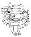
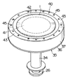
図2および図4に詳示されているように、回転ドラム35の回転筒37の上端にはサセプタ40が回転筒37の上端開口を閉塞するように被せられている。サセプタ40は円板形状の中央部材41と円形リング形状の第一周辺部材42および第二周辺部材43とが一枚の円板を構成するように同心円に配置されて、隣接した外周縁辺と内周縁辺とにそれぞれ形成された段付き部が上下で係合されて内側のものが外側のものに支持されるように組み合わて構成されている。
【0020】
中央部材41は炭化シリコンや窒化アルミニウムが使用されて、外径がウエハ1の外径よりも小径円板形状に形成されている。中央部材41を外側で支持した第一周辺部材42は炭化シリコンや窒化アルミニウムが使用されて、内径が中央部材41の外径と等しく外径がウエハ1の外径よりも大きい円形リング形状に形成されている。第一周辺部材42を外側で支持した第二周辺部材43は石英が使用されて、内径が第一周辺部材42の外径と等しく外径が回転筒37の内径よりも若干大きめの円形リング形状に形成されている。
【0021】
第一周辺部材42および第二周辺部材43の上面は中央部材41の上面よりもウエハ1の厚さの分だけ若干上げられている。つまり、第一周辺部材42および第二周辺部材43の上面は中央部材41の上面に載せられたウエハ1の上面と一致するようになっている。第一周辺部材42の上面および第二周辺部材43の上面には三本の案内溝44が周方向に等間隔に配置されて放射状に延在するようにそれぞれ没設されており、各案内溝44は後記するウエハ昇降装置50の係合部材53を径方向に摺動自在に挿入し得るように構成されている。
【0022】
第二周辺部材43には複数個の窒素ガス吹出口45が周方向に等間隔に配置されて上下方向に貫通するように開設されており、各窒素ガス吹出口45は回転ドラム35の内部に支持軸26の筒中空部を通じて供給された窒素ガス4をサセプタ40の上に全周にわたって均等に吹き出すように構成されている。
【0023】
図2および図4に詳しく示されているように、回転ドラム35の外側には被処理基板としてのウエハ1をサセプタ40および加熱ユニット27に対して昇降させるウエハ昇降装置50が設置されている。すなわち、ウエハ昇降装置50は円形リング形状に形成された昇降リング51を備えており、昇降リング51は回転ドラム35の外周に近接して同心円に配置されている。昇降リング51の上端面には三本の支柱52が周方向に等間隔に配置されて垂直方向上向きに立脚されており、三本の支柱52はウエハ搬入搬出口16におけるウエハ1の搬入搬出作業を妨げない位置にそれぞれ配設されている。つまり、三本の支柱52はウエハ搬入搬出口16に挿入されるウエハ移載装置のツィーザ2に干渉しないようになっている。
【0024】
各支柱52には各係合部材53が径方向内向きの放射状に延在するようにそれぞれ水平に突設されており、各係合部材53はサセプタ40の各案内溝44に出入り自在に上から嵌入するようになっている。各係合部材53の先端部には係合爪54が薄く形成されており、係合爪54はサセプタ40の中央部材41に載置されたウエハ1の外周縁部下面に下側から係合し得るように設定されている。
【0025】
昇降リング51の下端面には三本の突合部材55が周方向に等間隔に配置されて垂直方向下向きにそれぞれ垂下されており、これら突合部材55の下端面はチャンバ12の下側カップ13の内周面におけるウエハ搬入搬出口16よりも下側に段形状に形成されたチャンバ側突合部56に突合自在に対向されている。各突合部材55は回転筒37の外周に突設されたガイド57に適当なクリアランスをもってそれぞれ嵌入されることにより、回転ドラム35に対する昇降リング51の周方向を位置決めするとともに、昇降を案内するようになっている。
【0026】
次に、以上の構成に係る枚葉式CVD装置の作用を説明することにより、本発明の一実施の形態であるCVD膜形成方法を説明する。
【0027】
図1および図2に示されているように、ウエハ1の搬出時に回転ドラム35および加熱ユニット27が回転軸34および支持軸26によって下限位置に下降されると、ウエハ昇降装置50の突合部材55がチャンバ側突合部56に突合するため、昇降リング51が回転ドラム35に対して上昇する。この昇降リング51の上昇に伴って、昇降リング51に固定された三本の係合部材53がウエハ1を三方から支持してサセプタ40から浮き上がらせる状態になる。
【0028】
このようにウエハ昇降装置50がウエハ1をサセプタ40の上面から浮き上がらせた状態になると、ウエハ1の下方空間すなわちウエハ1の下面とサセプタ40の上面との間に挿入スペースが形成された状態になるため、ウエハ移載装置のツィーザ2がウエハ搬入搬出口16からウエハ1の挿入スペースに挿入される。この際、三本の係合部材53を支持した各支柱52はウエハ搬入搬出口16に挿入されるウエハ移載装置のツィーザ2に干渉しない。
【0029】
図2に示されているように、ウエハ1の下方に挿入されたツィーザ2は上昇することによりウエハ1を移載して受け取る。ウエハ1を受け取ったツィーザ2はウエハ搬入搬出口16を後退してウエハ1を処理室11から搬出する。ツィーザ2によってウエハ1を搬出したウエハ移載装置は処理室11の外部の空ウエハカセット等の所定の収納場所(図示せず)にウエハ1を移載する。
【0030】
その後、ウエハ移載装置は実ウエハカセット等の所定の収納場所(図示せず)から、次回に成膜処理するウエハ1をツィーザ2によって受け取って、ウエハ搬入搬出口16から処理室11に搬入する。図2に示されているように、ツィーザ2はウエハ1を三本の係合部材53の上方においてウエハ1の中心がサセプタ40の中心と一致する位置に搬送する。ウエハ1を所定の位置に搬送すると、ツィーザ2は若干下降することによりウエハ1を三本の係合部材53に移載する。この際、三本の係合部材53は先端部の薄い係合爪54をウエハ1の外縁に下から僅かに係合することにより、ウエハ1の受け取った状態になる。
【0031】
このようにしてウエハ1をウエハ昇降装置50に受け渡したツィーザ2は、ウエハ搬入搬出口16から処理室11外へ退出する。ツィーザ2が処理室11から退出すると、ウエハ搬入搬出口16はゲートバルブ17によって閉じられる。
【0032】
図3に示されているように、ゲートバルブ17が閉じられると、回転ドラム35および加熱ユニット27が回転軸34および支持軸26によって処理室11に対して上昇される。回転ドラム35の上昇初期においては、三本の突合部材55がチャンバ側突合部56の上に載った状態になっているため、ウエハ昇降装置50は回転ドラム35の上昇に追従せずに停止した状態になっている。つまり、ウエハ昇降装置50に支持されたウエハ1は回転ドラム35の上昇に伴ってサセプタ40に対して相対的に下降することになる。
【0033】
図4に示されているように、回転ドラム35の上昇に伴ってウエハ1がサセプタ40の所まで相対的に下降すると、三本の係合部材53は回転ドラム35の上面の案内溝44に嵌入した状態になり、下から支持しているウエハ1をサセプタ40の上に移載する。このウエハ1がサセプタ40に移載された状態において、ウエハ1の上面と、第一周辺部材42の上面、第二周辺部材43の上面および三本の係合部材53の上面とは一致した状態になっている。
【0034】
図3に示されているように、三本の係合部材53が回転ドラム35の上面の案内溝44に嵌入した後は、ウエハ昇降装置50は回転ドラム35に持ち上げられて一緒に処理室11を上昇して行く。この上昇に伴って、三本の突合部材55はチャンバ側突合部56から離れる。
【0035】
サセプタ40に移載されたウエハ1はヒータ30によって加熱されるとともに、ヒータ30の温度およびウエハ1の温度が熱電対33によって測定される。そして、ヒータ30の加熱量は熱電対33の測定結果に従ってフィードバック制御される。この際、三本の係合部材53は薄い係合爪54においてウエハ1の外縁に僅かに接触しているだけであるため、ヒータ30の加熱に影響を及ぼすことはなく、ウエハ1の温度分布は係合部材53の存在にかかわらず全体にわたって均一になる。また、最外周の第二周辺部材43は石英によって形成されているため、ウエハ1の熱が外方に逃げる現象が防止される。
【0036】
回転ドラム35および加熱ユニット27は処理室11を回転軸34および支持軸26によって上昇されて、ウエハ1の上面がプレート22の下面に近接する高さに停止される。
【0037】
また、排気口18が真空排気装置によって排気されるとともに、回転ドラム35が回転軸34によって回転される。排気口18の排気量および回転ドラム35の回転が安定した時点で、処理ガス3がガス導入口21に導入される。さらに、窒素ガス4が窒素ガス吹出口45からそれぞれ均等に吹き出される。
【0038】
ガス導入口21に導入された処理ガス3はガス溜め24に作用する排気口18の排気力によってガス溜め24に流入するとともに、径方向外向きに放射状に拡散して、プレート22の各吹出口23からそれぞれが略均等な流れになって、ウエハ1に向かってシャワー状に吹き出す。吹出口23群からシャワー状に吹き出した処理ガス3は排気口18に吸い込まれて排気されて行く。
【0039】
この際、回転ドラム35に支持されたサセプタ40上のウエハ1は回転しているため、吹出口23群からシャワー状に吹き出した処理ガス3はウエハ1の全面にわたって均等に接触する状態になる。また、ウエハ1の上面とその外側領域のサセプタ40の上面とは一致しているため、処理ガス3の流れは乱れが防止され均一に制御される。ここで、処理ガス3の熱化学反応による成膜レートは処理ガス3のウエハ1に対する接触量に依存するため、処理ガス3がウエハ1の全面にわたって均等に接触すれば、ウエハ1に処理ガス3によって形成されるCVD膜の膜厚分布や膜質分布はウエハ1の全面にわたって均一になる。
【0040】
また、加熱ユニット27は支持軸26に支持されることにより回転しない状態になっているため、回転ドラム35によって回転されながら加熱ユニット27によって加熱されるウエハ1の温度分布は周方向において均一に制御される。ここで、熱化学反応による成膜レートはウエハ1の温度分布に依存するため、ウエハ1の温度分布が全面にわたって均一であれば、ウエハ1に熱化学反応によって形成されるCVD膜の膜厚分布や膜質分布はウエハ1の全面にわたって均一に制御される。
【0041】
なお、窒素ガス4が各窒素ガス吹出口45から吹き出されていることにより、回転ドラム35の内部には窒素ガス4が充満した状態になっているため、処理ガス3が回転ドラム35の内部に侵入することは防止される。したがって、回転ドラム35の内部に侵入した処理ガス3によって加熱ユニット27のヒータ30が劣化されたり、処理ガス3が反射板31や熱電対33に付着してそれらの機能が損なわれたりする不具合が発生するのを未然に防止することができる。
【0042】
以上のようにしてCVD膜がウエハ1の全面にわたって均一に形成されて所定の処理時間が経過すると、図1に示されているように、回転ドラム35および加熱ユニット27は回転軸34および支持軸26によって搬入搬出位置に下降される。下降の途中において、ウエハ昇降装置50の三本の突合部材55がチャンバ側突合部56に突合するため、前述した作動により、ウエハ昇降装置50はウエハ1をサセプタ40の上から浮き上げる。
【0043】
以降、前述した作業が繰り返されることにより、ウエハ1にCVD膜が枚葉式CVD装置10によって枚葉処理されて行く。
【0044】
前記実施形態によれば、次の効果が得られる。
【0045】
(1)ウエハ1を保持したサセプタ40を回転させることにより、処理ガス3をウエハ1の全面にわたって均等に接触させることができるため、処理ガス3によってウエハ1に形成されるCVD膜の膜厚分布や膜質分布を全面にわたって均一に制御することができる。
【0046】
(2)ウエハ1を保持したサセプタ40を回転させるとともに加熱ユニット27を停止させることにより、サセプタ40によって回転されながら加熱ユニット27によって加熱されるウエハ1の温度分布を周方向において均一に制御することができるため、ウエハ1に熱化学反応によって形成されるCVD膜の膜厚分布や膜質分布をウエハ1の全面にわたって均一に制御することができる。
【0047】
(3)加熱ユニット27を回転させないことにより、加熱ユニット27の内部にヒータ30や熱電対33を設置することができるとともに、ヒータ30や熱電対33のための電気配線を加熱ユニット27に容易に敷設することができる。
【0048】
(4)ウエハ1のサセプタ40に対する授受に際して、ウエハ昇降装置50がウエハ1を昇降させてウエハ1の下面とサセプタ40の下面に挿入スペースを形成することにより、その挿入スペースにツィーザ2を挿入することができるため、ウエハ1をツィーザ2によって下側から機械的に支持することができ、ウエハ1を機械式ウエハ移載装置によって授受することができる。
【0049】
(5)前記(4)により、ウエハ移載装置として構造が複雑な真空吸着保持装置を使用した真空吸着式ウエハ移載装置または静電吸着保持装置を使用した静電吸着式ウエハ移載装置を採用しなくても済むため、枚葉式CVD装置の製造コストを大幅に低減することができ、また、適用範囲が制限されることもなく、常圧CVD装置や減圧CVD装置およびプラズマCVD装置等の基板処理装置全般に適用することができる。ちなみに、真空吸着保持装置は非接触形真空吸着保持装置を含めてウエハの上下面の差圧によってウエハを保持するため、減圧室では使用することができない。また、静電吸着保持装置は静電気を利用してウエハを吸着するため、静電破壊の危惧がある場合には使用することができないし、除電装置や帯電防止装置等が必要になり、その構造や運用が複雑になる。
【0050】
(6)ウエハ昇降装置50を回転ドラム35の外側に配置して三本の係合部材53の薄い係合爪54をウエハ1の外縁に僅かに係合させてウエハ1を下側から支持することにより、ウエハ昇降装置50の加熱ユニット27の加熱に及ぼす影響を抑止することができるため、ウエハ1の温度分布をウエハ昇降装置50の存在にかかわらず全体にわたって均一に制御することができる。
【0051】
(7)サセプタ40の最外周の第二周辺部材43を石英によって形成することにより、サセプタ40の上に載置されて加熱ユニット27によって加熱されたウエハ1の熱が外方に逃げるのを防止することができるため、ウエハ1の温度分布を全体にわたって均一に制御することができる。
【0052】
(8)サセプタ40の外周辺部の上面をサセプタ40上のウエハ1の上面と一致させることにより、処理ガス3の流れが乱れるのを防止することができるため、ウエハ1に処理ガス3によって形成されるCVD膜の膜厚分布や膜質分布をウエハ1の全面にわたって均一に制御することができる。
【0053】
(9)サセプタ40の最外周の第二周辺部材43に複数個の窒素ガス吹出口45を周方向に等間隔に開設し、サセプタ40を支持した回転ドラム35に窒素ガス4を供給して各窒素ガス吹出口45から吹き出させることにより、処理ガス3が回転ドラム35の内部に侵入するのを防止することができるため、回転ドラム35の内部に侵入した処理ガス3によって加熱ユニット27のヒータ30が劣化されたり、処理ガス3が反射板31や熱電対33に付着してそれらの機能を損なう不具合が発生するのを未然に防止することができる。
【0054】
(10)ウエハ1のサセプタ40に対する授受に際して、サセプタ40と加熱ユニット27とを両者の距離を保って昇降させることにより、サセプタ40に対する加熱状態を常に一定とすることができるため、温度安定性の向上を図ることができる。
【0055】
なお、前記実施の形態においては、ウエハ昇降装置50の突合部材55がチャンバ12の下側カップ13の側壁に段状に形成された突合部56に突合されているが、突合部材55は処理室11の底面(ボトムキャップ15の上面)に突合するように構成してもよい。
【0056】
次に、本発明の実施の形態2を図5〜図10に即して説明する。
【0057】
本実施の形態2が前記実施の形態1と異なる主な点は、被処理基板としてのウエハをサセプタおよび加熱ユニットに対して昇降させるウエハ昇降装置が回転ドラムの内側に設置されている点である。
【0058】
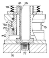
すなわち、図5〜図9に示されているように、この内側配置形のウエハ昇降装置60はチャンバ12の底壁上(ボトムキャップ15の上面)に垂直方向上向きに固定された三本の突き上げピン(以下、固定側ピンという。)61を備えており、三本の固定側ピン61はウエハ搬入搬出口16に対するウエハ1の搬入搬出作業を邪魔しない位置に配設されている。つまり、三本の固定側ピン61の配置はウエハ搬入搬出口16に挿入されるウエハ移載装置のツィーザ2に干渉しない位置になっている。
【0059】
図9に詳示されているように、固定側ピン61はピン部62の長い画鋲形状に形成されており、鍔部63の下面がボトムキャップ15の上面に当接されて垂直方向上向きに立脚されている。ピン部62の外周には座板64が嵌合されており、座板64は鍔部63の上面に載置された状態になっている。ピン部62の長さはウエハのサセプタ上からの突き上げ量に対応するように設定されており、ピン部62の太さは回転ドラム35の回転板36に開設された挿通孔65および加熱ユニット27の筐体27Aに開設された挿通孔66に挿入し得るように設定されている。
【0060】
回転ドラム35の回転板36に開設された挿通孔(以下、回転側挿通孔という。)65は三個が、回転ドラム35が昇降する位置において三本の固定側ピン61にそれぞれ対向するように配置されている。加熱ユニット27の筐体27Aに開設された挿通孔(以下、固定側挿通孔という。)66は三個が、三本の固定側ピン61にそれぞれ対向するように配置されている。つまり、回転ドラム35が昇降する位置において、三本の固定側ピン61は三個の回転側挿通孔65および三個の固定側挿通孔66をそれぞれ挿通し得るように構成されている。
【0061】
加熱ユニット27の支持板28には三個のガイド孔68が各固定側挿通孔66にそれぞれ対向するように開設されており、各ガイド孔68にはウエハをサセプタから突き上げる突き上げピン(以下、可動側ピンという。)69のそれぞれが上下方向に摺動自在に嵌入されている。可動側ピン69は大径部と小径部とを有する丸棒形状に形成されており、大径部の下端部には鍔部70が形成されている。鍔部70は固定側挿通孔66の上端部に形成された支持穴67の底面に離着座自在に対向されている。可動側ピン69の上端部の小径部は突上部71を形成しており、突上部71は反射板31、ヒータ30およびサセプタ40を挿通するようになっている。
【0062】
すなわち、反射板31、ヒータ30およびサセプタ40における三本の可動側ピン69にそれぞれ対向する三箇所には、挿通孔72、73、74が突上部71を挿通し得るように開設されている。図6に示されているように、サセプタ40に開設された三個の挿通孔74はサセプタ40の中央部材41の外周辺部にそれぞれ配置されており、周方向における三個の挿通孔74の配置は三個の固定側ピン61の配置に対向していることから、ウエハ搬入搬出口16に挿入されるウエハ移載装置のツィーザ2に干渉しない位置になっている。
【0063】
次に、以上の構成に係る枚葉式CVD装置の作用を説明することにより、本発明の一実施の形態であるCVD膜形成方法を説明する。
【0064】
図5に示されているように、ウエハ1の搬出時に回転ドラム35および加熱ユニット27が回転軸34および支持軸26によって下限位置に下降されると、ウエハ昇降装置60の三本の可動側ピン69は対向する各固定側ピン61にそれぞれ突合することにより、回転ドラム35および加熱ユニット27に対して上昇する。上昇した三本の可動側ピン69はウエハ1を下方から支持してサセプタ40から浮き上がらせる状態になる。
【0065】
図9(a)に示されているように、ウエハ昇降装置60がウエハ1をサセプタ40の上面から浮き上がらせた状態になると、ウエハ1の下方空間すなわちウエハ1の下面とサセプタ40の上面との間に挿入スペースが形成された状態になるため、ウエハ移載装置のツィーザ2がウエハ搬入搬出口16からウエハ1の挿入スペースに挿入される。この際、図6に示されているように、三本の可動側ピン69はいずれもウエハ搬入搬出口16に挿入されるウエハ移載装置のツィーザ2に干渉しない。
【0066】
図6に示されているように、ウエハ1の下方に挿入されたツィーザ2は上昇することによりウエハ1を移載して受け取る。ウエハ1を受け取ったツィーザ2はウエハ搬入搬出口16を後退してウエハ1を処理室11から搬出する。ツィーザ2によってウエハ1を搬出したウエハ移載装置は処理室11の外部の空ウエハカセット等の所定の収納場所(図示せず)にウエハ1を移載する。
【0067】
その後、ウエハ移載装置は実ウエハカセット等の所定の収納場所(図示せず)から次回に成膜処理するウエハ1をツィーザ2によって受け取って、ウエハ搬入搬出口16から処理室11に搬入する。ツィーザ2はウエハ1を三本の可動側ピン69の上方においてウエハ1の中心がサセプタ40の中心と一致する位置に搬送する。ウエハ1を所定の位置に搬送すると、ツィーザ2は若干下降することによりウエハ1を三本の可動側ピン69に移載する。この際、三本の可動側ピン69の先端部は小径に形成されているため、ウエハ1の下面に極僅かに接触することにより、ウエハ1の受け取った状態になる。
【0068】
このようにしてウエハ1をウエハ昇降装置60に受け渡したツィーザ2は、ウエハ搬入搬出口16から処理室11外へ退出する。ツィーザ2が処理室11から退出すると、ウエハ搬入搬出口16はゲートバルブ17によって閉じられる。
【0069】
図7に示されているように、ゲートバルブ17が閉じられると、回転ドラム35および加熱ユニット27が回転軸34および支持軸26によって処理室11に対して上昇される。回転ドラム35の上昇の初期において、三本の可動側ピン69は固定側ピン61の上に載った状態になっているため、回転ドラム35の上昇に伴って回転ドラム35に対して相対的に徐々に下降することになる。
【0070】
図9(b)に示されているように、三本の可動側ピン69が固定側ピン61から離座すると、三本の可動側ピン69はサセプタ40の挿通孔74に引き込まれた状態になり、下から支持しているウエハ1をサセプタ40の上に移載する。このウエハ1がサセプタ40に移載された状態において、三本の可動ピン69はサセプタ40の挿通孔74から下方に抜け出て離れた状態になっている。また、図8に示されているように、ウエハ1の上面と、第一周辺部材42の上面および第二周辺部材43の上面とは一致した状態になっている。
【0071】
サセプタ40に移載されたウエハ1はヒータ30によって加熱されるとともに、ヒータ30の温度およびウエハ1の温度が熱電対33によって測定される。そして、ヒータ30の加熱量は熱電対33の測定結果に従ってフィードバック制御される。この際、三本の可動側ピン69を挿通するためのサセプタの挿通孔74はウエハ1の外縁で僅かに開口しているだけであるため、ヒータ30の加熱に影響を及ぼすことはなく、ウエハ1の温度分布は三個の挿通孔74の存在にかかわらず全体にわたって均一になる。
【0072】
図7に示されているように、回転ドラム35および加熱ユニット27は処理室11を回転軸34および支持軸26によって上昇されて、ウエハ1の上面がプレート22の下面に近接する高さに停止される。
【0073】
排気口18が真空排気装置によって排気されるとともに、回転ドラム35が回転軸34によって回転される。排気口18の排気量および回転ドラム35の回転作動が安定した時点で、処理ガス3がガス導入口21に導入される。ガス導入口21に導入された処理ガス3はガス溜め24に作用する排気口18の排気力によってガス溜め24に流入するとともに、径方向外向きに放射状に拡散して、プレート22の各吹出口23からそれぞれが略均等な流れになって、ウエハ1に向かってシャワー状に吹き出す。吹出口23群からシャワー状に吹き出した処理ガス3は排気口18に吸い込まれて排気されて行く。
【0074】
この際、回転ドラム35に支持されたサセプタ40上のウエハ1は回転しているため、吹出口23群からシャワー状に吹き出した処理ガス3はウエハ1の全面にわたって均等に接触する状態になる。また、ウエハ1の上面とその外側領域のサセプタ40の上面とは一致しているため、処理ガス3の流れは乱れが防止され均一に制御される。このようにして処理ガス3がウエハ1の全面にわたって均等に接触するため、ウエハ1に処理ガス3によって形成されるCVD膜の膜厚分布や膜質分布はウエハ1の全面にわたって均一になる。
【0075】
また、加熱ユニット27は支持軸26に支持されることにより回転しない状態になっているため、回転ドラム35によって回転されながら加熱ユニット27によって加熱されるウエハ1の温度分布は周方向において均一に制御される。そして、ウエハ1の温度分布が全面にわたって均一に制御されることにより、ウエハ1に熱化学反応によって形成されるCVD膜の膜厚分布や膜質分布はウエハ1の全面にわたって均一に制御される。
【0076】
ちなみに、三本の可動側ピン69は加熱ユニット27のガイド孔68および支持穴67に支持されているため、加熱ユニット27と共に停止している。また、固定側ピン61はチャンバ12のボトムキャップ15に固定されているため、停止している。
【0077】
以上のようにしてCVD膜がウエハ1の全面にわたって均一に形成されて所定の処理時間が経過すると、回転ドラム35の回転が所定の搬入搬出位置に対応する位相で停止される。続いて、図5に示されているように、回転ドラム35および加熱ユニット27は回転軸34および支持軸26によって搬入搬出位置に下降される。下降の途中において、ウエハ昇降装置60の三本の可動側ピン69が固定側ピン61に突合するため、前述した作動により、ウエハ昇降装置60はウエハ1をサセプタ40の上から浮き上げる。
【0078】
以降、前述した作業が繰り返されることにより、ウエハ1にCVD膜が枚葉式CVD装置10によって枚葉処理されて行く。
【0079】
以上説明したように、本実施の形態2においては、ウエハ1のサセプタ40の授受に際して、ウエハ昇降装置60がウエハ1を昇降させてウエハ1の下面とサセプタ40の下面に挿入スペースを形成することにより、その挿入スペースにツィーザ2を挿入することができるため、ウエハ1をツィーザ2によって下側から機械的に支持することができる。つまり、本実施の形態2においても、ウエハ1をサセプタ40に機械式ウエハ移載装置によって授受することができる。
【0080】
また、ウエハ1を保持したサセプタ40を回転させることにより、処理ガス3をウエハ1の全面にわたって均等に接触させることができるため、処理ガス3によってウエハ1に形成されるCVD膜の膜厚分布や膜質分布を全面にわたって均一に制御することができる。
【0081】
ウエハ1を保持したサセプタ40を回転させるとともに、加熱ユニット27を停止させることにより、サセプタ40によって回転されながら加熱ユニット27によって加熱されるウエハ1の温度分布を周方向において均一に制御することができるため、ウエハ1に熱化学反応によって形成されるCVD膜の膜厚分布や膜質分布をウエハ1の全面にわたって均一に制御することができる。
【0082】
加熱ユニット27を回転させないことにより、加熱ユニット27の内部にヒータ30や熱電対33を設置することができるとともに、ヒータ30や熱電対33のための電気配線を加熱ユニット27に容易に敷設することができる。
【0083】
ウエハ1をサセプタ40に対して昇降させるウエハ昇降装置60がサセプタ40の内径側に配置されているため、ウエハ昇降装置60が回転ドラム35の外側に突出するのを回避することができ、処理室11の容積が大きくなるのを防止することができる。
【0084】
また、ウエハ1のサセプタ40に対する授受に際して、サセプタ40と加熱ユニット27とを両者の距離を保って昇降させることにより、サセプタ40に対する加熱状態を常に一定とすることができるため、温度安定性の向上を図ることができる。
【0085】
次に、支持軸を固定しつつ回転軸を回転させる回転駆動装置の一実施の形態を図10について説明する。
【0086】
図10に示されている回転駆動装置は出力軸が中空軸に形成された中空軸電動モータ(以下、モータという。)75を備えており、このモータ75の中空の出力軸が回転ドラム35を回転させる回転軸34として構成されている。モータ75のハウジング75aはエアシリンダ装置等から構築されて一部のみが図示されたエレベータの昇降台76に垂直方向上向きに据え置きされており、昇降台76によって枚葉式CVD装置のチャンバ12に対して昇降されるように構成されている。ハウジング75aの内周面には固定子(ステータ)75bが固定されており、固定子75bの内側にはモータ75の回転子(アーマチュア)75cがエアギャップを設定されて同心円に配置されハウジング75aによって回転自在に支承されている。回転子75cには中空の出力軸である回転軸34が一体回転するように固定されており、回転軸34の中心線上には支持軸26が配置されてハウジング75aに固定されている。
【0087】
なお、支持軸26の下端開口には支持軸26の中空部すなわち処理室11の内外を流体的に隔絶するためのハーメチックシール77が装着されており、ハーメチックシール77によってヒータ30や熱電対33の電気配線(図示せず)が支持軸26の中空部から引き出されるようになっている。また、回転軸34の外側にはチャンバ12の挿通孔25をシールするためのベローズ78が同心円に配置されており、ベローズ78の上下端はチャンバ12のボトムキャップ15の下面および回転軸34のフランジの上面にそれぞれ締結されている。
【0088】
以上の構成に係る回転駆動装置によれば、支持軸26を固定しつつ回転軸34を回転させることができるため、支持軸26によって加熱ユニット27を支持するとともに、回転軸34によって回転ドラム35を支持することにより、加熱ユニット27を停止させつつ、サセプタ40すなわちウエハ1を回転させることができる。
【0089】
次に、本発明の実施の形態3を図11〜図15に即して説明する。
【0090】
本実施の形態3が前記実施の形態1と異なる主な点は、ウエハ昇降装置が回転ドラムの内側に設置されているとともに、ウエハをサセプタの中央部材を介して昇降させるように構成されており、また、ヒータが分割されている点である。
【0091】
すなわち、図11〜図14に示されているように、この内側配置形のウエハ昇降装置80は円形リング形状に形成された昇降リング81を備えており、昇降リング81は回転ドラム35の回転板36の上に支持軸26と同心円に配置されている。昇降リング(以下、回転側リングという。)81の下面には複数本(本実施の形態においては三本とする。)の突き上げピン(以下、回転側ピンという。)82が周方向に等間隔に配置されて垂直方向下向きに突設されており、各可動側ピン69は回転板36に回転軸34と同心円上に配置されて垂直方向に開設された各ガイド孔83にそれぞれ摺動自在に嵌入されている。
【0092】
各可動側ピン69の長さは回転側リング81を水平に突き上げ得るように互いに等しく設定されているとともに、ウエハのサセプタ上からの突き上げ量に対応するように設定されている。各可動側ピン69の下端は処理室11の底面すなわちボトムキャップ15の上面に離着座自在に対向されている。
【0093】
加熱ユニット27の支持板28には円形リング形状に形成された第二の昇降リング(以下、ヒータ側リングという。)84が支持軸26と同心円に配置されている。ヒータ側リング84の下面には複数本(本実施の形態においては三本とする。)の突き上げピン(以下、ヒータ側ピンという。)85が周方向に等間隔に配置されて垂直方向下向きに突設されており、各ヒータ側ピン85は支持板28に支持軸26と同心円上に配置されて垂直方向に開設された各ガイド孔86にそれぞれ摺動自在に嵌入されている。
【0094】
各ヒータ側ピン85の長さはヒータ側リング84を水平に突き上げ得るように互いに等しく設定されているとともに、その下端が回転側リング81の上面に適度のエアギャップを置いて対向されている。つまり、各ヒータ側ピン85は回転ドラム35の回転時に回転側リング81に干渉しないようになっている。
【0095】
ヒータ側リング84の上面には複数本(本実施の形態においては三本とする。)の突き上げピン(以下、突上部という。)87が周方向に等間隔に配置されて垂直方向上向きに突設されており、突上部87の上端は反射板31、ヒータ30およびサセプタ40を挿通してサセプタ40の中央部材41の下面に対向するようになっている。各突上部87の長さは中央部材41を水平に突き上げ得るように互いに等しく設定されているとともに、ヒータ側リング84が支持板28に着座した状態において、その上端が中央部材41の上面に適度のエアギャップを置いて対向するように設定されている。つまり、各突上部87は回転ドラム35の回転時にサセプタ40に干渉しないようになっている。
【0096】
なお、図示の便宜上、図13においては突上部87の上端がヒータ30の上側に位置しているが、図15(a)に想像線で示されているように、突上部87の上端は加熱ユニット27の加熱効果の観点からはヒータ30および反射板31の下方に位置させることが望ましい。すなわち、突上部87がヒータ30および反射板31の上方に突き出ていると、ヒータ30および反射板31の熱線を遮蔽する虞があるからである。
【0097】
図15に詳示されているように、本実施の形態においては、加熱ユニット27のヒータ30はサセプタ40の中央部材41に対応する中央ヒータ部材30aと、サセプタ40の第一周辺部材42および第二周辺部材43に対応する周辺ヒータ部材30bとに分割されており、中央ヒータ部材30aと周辺ヒータ部材30bとは出力を独立して制御し得るように構成されている。
【0098】
次に、以上の構成に係る枚葉式CVD装置の作用を説明することにより、本発明の一実施の形態であるCVD膜形成方法を説明する。
【0099】
図11に示されているように、ウエハ1の搬出時に回転ドラム35および加熱ユニット27が回転軸34および支持軸26によって下限位置に下降されると、ウエハ昇降装置80の回転側ピン82の下端が処理室11の底面すなわちボトムキャップ15の上面に突合するため、回転側リング81が回転ドラム35および加熱ユニット27に対して相対的に上昇する。上昇した回転側リング81はヒータ側ピン85を突き上げることにより、ヒータ側リング84を持ち上げる。ヒータ側リング84が持ち上げられると、ヒータ側リング84に立脚された三本の突上部87がサセプタ40の中央部材41を下方から支持して第一周辺部材42および第二周辺部材43から浮き上がらせる。この中央部材41にはウエハ1の中央部が載置されているため、ウエハ1は浮き上がった状態になる。
【0100】
図12に示されているように、ウエハ昇降装置80がウエハ1をサセプタ40の上面から浮き上がらせた状態になると、ウエハ1の下方空間すなわちウエハ1の下面とサセプタ40の上面との間に挿入スペースが形成された状態になるため、ウエハ移載装置のフォーク形のツィーザ2Aがウエハ搬入搬出口16からウエハ1の挿入スペースに挿入される。この際、ウエハ1の中央部がサセプタ40の中央部材41によって支持されているため、ツィーザ2Aとしては図12に示されているようにフォーク形状のものが使用される。すなわち、ツィーザ2Aはウエハ1の中央部の中央部材41と干渉しない状態になる。
【0101】
図12に示されているように、ウエハ1の下方に挿入されたツィーザ2Aは上昇することによりウエハ1を移載して受け取る。この際、フォーク形状のツィーザ2Aはウエハ1の下面における外周辺部を受ける。ウエハ1を受け取ったツィーザ2Aはウエハ搬入搬出口16を後退してウエハ1を処理室11から搬出する。そして、ツィーザ2Aによってウエハ1を搬出したウエハ移載装置は、処理室11の外部の空ウエハカセット等の所定の収納場所(図示せず)にウエハ1を移載する。
【0102】
その後、ウエハ移載装置は実ウエハカセット等の所定の収納場所(図示せず)から次回に成膜処理するウエハ1をツィーザ2Aによって受け取って、ウエハ搬入搬出口16から処理室11に搬入する。ツィーザ2Aはウエハ1をサセプタ40の中央部材41の上方においてウエハ1の中心が中央部材41の中心と一致する位置に搬送する。ウエハ1を所定の位置に搬送すると、ツィーザ2Aは若干下降することによりウエハ1を中央部材41に移載する。
【0103】
ところで、搬入されて来たばかりのウエハ1は低温度の状態になっているため、ウエハ1が移載されると、中央部材41の温度は低下することになる。そして、図15(c)に示されているように、ヒータ30が分割されずに同一出力をもってサセプタ40を全体的に均一に加熱するように構成されている場合には、ウエハ1によって冷却された中央部材41はそのまま下降してヒータ30によって第一周辺部材42および第二周辺部材43と均等に加熱されることになるため、ウエハ1の中央部は中央部材41が冷却された分だけ周辺部よりも低温となり、ウエハ1の温度分布が不均一になる。その結果、ウエハ1に形成されるCVD膜の膜厚分布や膜質分布が不均一になってしまう。
【0104】
そこで、本実施の形態においては、図15(b)に示されているように、中央部材41が上昇してウエハ1を受け取る際には、分割されたヒータ30の中央ヒータ部材30Aの出力を高めて中央部材41を余分に加熱することにより、中央部材41が低温度のウエハ1を受け取った時に相対的に冷却されて温度が低下するのを防止する。このようにしてウエハ1を受け取った時に中央部材41の温度が低下する現象を防止することにより、図15(a)に示されているように、中央部材41が下降した後に、中央部材41が第一周辺部材42および第二周辺部材43とヒータ30によって均等に加熱される場合であっても、ウエハ1の温度分布は均一になるため、ウエハ1に形成されるCVD膜の膜厚分布や膜質分布は全体にわたって均一になる。
【0105】
そして、ウエハ1をウエハ昇降装置80に受け渡したツィーザ2は、ウエハ搬入搬出口16から処理室11外へ退出する。ツィーザ2が処理室11から退出すると、ウエハ搬入搬出口16はゲートバルブ17によって閉じられる。
【0106】
図13に示されているように、ゲートバルブ17が閉じられると、処理室11に対して回転ドラム35および加熱ユニット27が回転軸34および支持軸26によって上昇される。回転ドラム35の上昇の初期において、回転側ピン82が処理室11の底面すなわちボトムキャップ15の上面に突合し、ヒータ側ピン85が回転側リング81の上に載った状態になっているため、回転側リング81の突上部87に支持された中央部材41は回転ドラム35の上昇に伴って回転ドラム35に対して相対的に徐々に下降することになる。
【0107】
回転側ピン82が処理室11の底面から離座すると、突上部87はサセプタ40の下方に引き込まれた状態になるため、図14に示されているように、中央部材41は第一周辺部材42の内側に嵌入する。この状態において、ウエハ1はサセプタ40の上に完全に移載された状態になり、ウエハ1の上面と、第一周辺部材42の上面および第二周辺部材43の上面とは一致した状態になる。
【0108】
サセプタ40に移載されたウエハ1はヒータ30によって加熱されるとともに、ヒータ30の温度およびウエハ1の温度が熱電対33によって測定される。そして、ヒータ30の加熱量は熱電対33の測定結果に従ってフィードバック制御される。この際、サセプタ40には突上部87を挿通するための挿通孔が開設されていないため、ウエハ1の温度分布はウエハ昇降装置80の存在にかかわらず全体にわたって均一になる。また、前述した通り、サセプタ40を受け取る際に中央部材41は予熱されているため、ウエハ1を中央部材41にて受け取ったにもかかわらず、ウエハ1の温度分布は全体にわたって均一になる。
【0109】
回転ドラム35および加熱ユニット27は処理室11を回転軸34および支持軸26によって上昇されて、ウエハ1の上面がプレート22の下面に近接する高さに停止される。また、排気口18が真空排気装置によって排気される。
【0110】
続いて、回転ドラム35が回転軸34によって回転される。このとき、回転側ピン82は処理室11の底面から離座し、ヒータ側ピン85は回転側リング81から離座しているため、回転ドラム35の回転がウエハ昇降装置80に妨げられることはなく、しかも、加熱ユニット27は停止状態を維持することができる。すなわち、ウエハ昇降装置80においては、回転側リング81が回転ドラム35と共に回転し、ヒータ側リング84が加熱ユニット27と共に停止した状態になっている。
【0111】
排気口18の排気量および回転ドラム35の回転作動が安定した時点で、処理ガス3がガス導入口21に導入される。ガス導入口21に導入された処理ガス3はガス溜め24に作用する排気口18の排気力によってガス溜め24に流入するとともに、径方向外向きに放射状に拡散して、プレート22の各吹出口23からそれぞれが略均等な流れになって、ウエハ1に向かってシャワー状に吹き出す。吹出口23群からシャワー状に吹き出した処理ガス3は排気口18に吸い込まれて排気されて行く。
【0112】
この際、回転ドラム35に支持されたサセプタ40上のウエハ1は回転しているため、吹出口23群からシャワー状に吹き出した処理ガス3はウエハ1の全面にわたって均等に接触する状態になる。また、ウエハ1の上面とその外側領域のサセプタ40の上面とは一致しているため、処理ガス3の流れは乱れが防止され均一に制御される。このようにして処理ガス3がウエハ1の全面にわたって均等に接触するため、ウエハ1に処理ガス3によって形成されるCVD膜の膜厚分布や膜質分布はウエハ1の全面にわたって均一になる。
【0113】
また、加熱ユニット27は支持軸26に支持されることにより回転しない状態になっているため、回転ドラム35によって回転されながら加熱ユニット27によって加熱されるウエハ1の温度分布は周方向において均一に制御される。しかも、サセプタ40には突上部87を挿通するための挿通孔が開設されていないため、かつまた、サセプタ40を受け取る際に中央部材41は予熱されているため、ウエハ1の温度分布は全体にわたって均一に制御される。このようにウエハ1の温度分布が全面にわたって均一に制御されることにより、ウエハ1に熱化学反応によって形成されるCVD膜の膜厚分布や膜質分布はウエハ1の全面にわたって均一に制御される。
【0114】
以上のようにしてCVD膜がウエハ1の全面にわたって均一に形成されて所定の処理時間が経過すると、図11に示されているように、回転ドラム35および加熱ユニット27は回転軸34および支持軸26によって搬入搬出位置に下降される。下降の途中において、ウエハ昇降装置80の回転側ピン82が処理室11の底面に突合し、ヒータ側ピン85が回転側リング81に突合するため、前述した作動により、ウエハ昇降装置80はウエハ1をサセプタ40の中央部材41の上昇によって浮き上げる。
【0115】
以降、前述した作業が繰り返されることにより、ウエハ1にCVD膜が枚葉式CVD装置10によって枚葉処理されて行く。
【0116】
以上説明したように、本実施の形態3においても、ウエハ1を機械式ウエハ移載装置によって授受することができる。また、ウエハ1を保持したサセプタ40を回転させることにより、処理ガス3をウエハ1の全面にわたって均等に接触させることができるため、処理ガス3によってウエハ1に形成されるCVD膜の膜厚分布や膜質分布を全面にわたって均一に制御することができる。さらに、ウエハ1を保持したサセプタ40を回転させるとともに、加熱ユニット27を停止させることにより、サセプタ40によって回転されながら加熱ユニット27によって加熱されるウエハ1の温度分布を周方向において均一に制御することができるため、ウエハ1に熱化学反応によって形成されるCVD膜の膜厚分布や膜質分布をウエハ1の全面にわたって均一に制御することができる。
【0117】
加熱ユニット27を回転させないことにより、加熱ユニット27の内部にヒータ30や熱電対33を設置することができるとともに、ヒータ30や熱電対33のための電気配線を加熱ユニット27に容易に敷設することができる。
【0118】
ウエハ1を昇降させるウエハ昇降装置80が回転ドラム35の内径側に配置されているため、ウエハ昇降装置80が回転ドラム35の外側に突出するのを回避することができ、処理室11の容積が大きくなるのを防止することができる。
【0119】
さらに、サセプタ40には突上部87を挿通するための挿通孔が開設されていないため、ウエハ1の温度分布をウエハ昇降装置80の存在にかかわらず全体にわたって均一に制御することができる。また、サセプタ40を受け取る際に中央部材41は予熱されるため、ウエハ1を中央部材41にて受け取るにもかかわらず、ウエハ1の温度分布を全体にわたって均一に制御することができる。
【0120】
次に、本発明の実施の形態4を図16および図17に即して説明する。
【0121】
本実施の形態4は前記実施の形態3に対して、ウエハ昇降装置90が回転側リング81を省略されている代わりに回転ドラム35が加熱ユニット27に対して昇降するように構成されている点が異なっている。
【0122】
すなわち、図16および図17に示されているように、加熱ユニット27を支持した支持軸26は処理室11に対して昇降するように構成されているとともに、回転ドラム35を支持した回転軸34に対しても独立して昇降するように構成されている。そして、ウエハ昇降装置90の昇降リング94の下面に垂直方向下向きに突設された突上ピン95は加熱ユニット27の支持板28に開設されたガイド孔96を挿通して、その下端が回転ドラム35の底面すなわち回転板36の上面に突合自在に対向されている。昇降リング94の上面に突設された突上部97の上端は反射板31、ヒータ30およびサセプタ40を挿通してサセプタ40の中央部材41の下面に対向するようになっている。つまり、突上ピン95および突上部97は回転ドラム35の回転時に回転ドラム35およびサセプタ40に干渉しないようになっている。
【0123】
図16に示されているように、ウエハ1の搬出搬入時には、回転ドラム35および加熱ユニット27が回転軸34および支持軸26によって処理室11の搬入搬出位置に下降され、かつ、回転ドラム35が回転軸34によって加熱ユニット27に対して下降される。回転ドラム35が加熱ユニット27に対して下降されると、ウエハ昇降装置90の昇降リング94が回転ドラム35に対して相対的に上昇する。昇降リング94が回転ドラム35に対して上昇すると、昇降リング94に立脚された三本の突上部97がサセプタ40の中央部材41を下方から支持して第一周辺部材42および第二周辺部材43から浮き上がらせる。この中央部材41にはウエハ1の中央部が載置されているため、ウエハ1は浮き上がった状態になる。
【0124】
図16に示されているように、ウエハ昇降装置90がウエハ1をサセプタ40の上面から浮き上がらせた状態になると、ウエハ1の下方空間すなわちウエハ1の下面とサセプタ40の上面との間に挿入スペースが形成された状態になるため、ウエハ移載装置のフォーク形のツィーザ2Aがウエハ搬入搬出口16からウエハ1の挿入スペースに挿入することができる。つまり、前記した実施の形態3と同様にして、機械式ウエハ移載装置によってウエハ1の授受を実行することができる。
【0125】
ウエハ1の授受後、図17に示されているように、処理室11に対して回転ドラム35および加熱ユニット27が回転軸34および支持軸26によって上昇され、かつ、回転ドラム35が回転軸34によって加熱ユニット27に対して上昇される。回転ドラム35が加熱ユニット27に対して上昇されると、昇降リング94の突上部97に支持された中央部材41は回転ドラム35に対して下降し、第一周辺部材42の内側に嵌入する。この状態において、ウエハ1はサセプタ40の上に移載された状態になり、ウエハ1の上面と、第一周辺部材42の上面および第二周辺部材43の上面とは一致した状態になる。
【0126】
その後、前記した実施の形態3と同様に、ウエハ1が回転ドラム35によって回転された状態で、ウエハ1に成膜処理が実施されて、ウエハ1に全体にわたって均一な処理が施される。この際、ウエハ昇降装置90の昇降リング94は加熱ユニット27と共に停止した状態になっており、突上ピン95の下端は回転ドラム35の底面から離座し、突上部97の上端はサセプタ40の下面から離れて回転ドラム35の回転を許容した状態になっている。
【0127】
以上のようにしてCVD膜がウエハ1の全面にわたって均一に形成されて所定の処理時間が経過すると、図16に示されているように、回転ドラム35および加熱ユニット27は回転軸34および支持軸26によって搬入搬出位置に下降されるとともに、回転ドラム35が加熱ユニット27に対して下降される。回転ドラム35が加熱ユニット27に対して下降されると、前述した作動により、ウエハ昇降装置90はウエハ1をサセプタ40の中央部材41の上昇によって浮き上げる。
【0128】
以降、前述した作業が繰り返されることにより、ウエハ1にCVD膜が枚葉式CVD装置10によって枚葉処理されて行く。
【0129】
以上説明したように、本実施の形態4によれば、前記実施の形態3に加えて、回転側リング81や回転側ピン82およびガイド孔83を省略することができるため、摺動部を低減することができるという効果を得ることができる。
【0130】
なお、本実施の形態4においては、ウエハ昇降装置90が回転ドラム35の加熱ユニット27に対しての昇降によってウエハ1を昇降させるように構成されているため、回転ドラム35および加熱ユニット27の処理室11に対する昇降に連動してウエハ1を自動的に昇降させる実施の形態1、2、3に比べて、回転軸34および支持軸26を昇降させるエレベータの構造が若干複雑になる。
【0131】
なお、本発明は前記実施の形態に限定されるものではなく、その要旨を逸脱しない範囲において、種々に変更が可能であることはいうまでもない。
【0132】
例えば、温度センサとしては、熱電対を使用するに限らず、他の非接触式温度センサを使用することができるし、省略してもよい。
【0133】
被処理基板はウエハに限らず、LCD装置の製造工程におけるガラス基板や液晶パネル等の基板であってもよい。
【0134】
本発明は、枚葉式コールドウオール形CVD装置に限らず、ドライエッチング装置等の基板処理装置全般に適用することができる。
【0135】
【発明の効果】
以上説明したように、本発明によれば、被処理基板の授受に機械式基板移載装置を使用することができ、他方、被処理基板に処理が施されるに際しては、サセプタで支持した被処理基板を回転させることにより、加熱ユニットの加熱による被処理基板上の温度分布を全体にわたって均一に制御し、被処理基板を処理室雰囲気に全体にわたって均一に接触させることができるため、被処理基板に均一な処理を施すことできる。
【図面の簡単な説明】
【図1】 本発明の一実施の形態である枚葉式CVD装置のウエハ搬入搬出工程を示す正面断面図である。
【図2】その主要部を示す斜視図である。
【図3】その枚葉式CVD装置の処理工程を示す正面断面図である。
【図4】その主要部を示す斜視図である。
【図5】本発明の実施の形態2である枚葉式CVD装置のウエハ搬入搬出工程を示す正面断面図である。
【図6】その主要部を示す斜視図である。
【図7】その枚葉式CVD装置の処理工程を示す一部切断正面図である。
【図8】その主要部を示す斜視図である。
【図9】ウエハ昇降装置の作用を説明するための各正面断面図であり、(a)はウエハ浮かせ時を示し、(b)はウエハ載置時を示している。
【図10】支持軸を固定し回転軸を回転させる回転駆動装置の一実施形態を示す一部切断正面図である。
【図11】本発明の実施の形態3である枚葉式CVD装置のウエハ搬入搬出工程を示す正面断面図である。
【図12】その主要部を示す斜視図である。
【図13】その枚葉式CVD装置の処理工程を示す一部切断正面図である。
【図14】その主要部を示す斜視図である。
【図15】ヒータの作用を説明するための各正面断面図であり、(a)は処理中の加熱作用を示し、(b)は搬入搬出時の加熱作用を示しており、(c)は比較例における搬入搬出時の加熱作用を示している。
【図16】本発明の実施の形態4である枚葉式CVD装置のウエハ搬入搬出工程を示す正面断面図である。
【図17】その枚葉式CVD装置の処理工程を示す一部切断正面図である。
【符号の説明】
1…ウエハ(被処理基板)、2…ウエハ移載装置のツィーザ、2A…フォーク形のツィーザ、3…処理ガス、4…窒素ガス、10…枚葉式CVD装置(基板処理装置)、11…処理室、12…チャンバ、13…下側カップ、14…上側カップ、15…ボトムキャップ、16…ウエハ搬入搬出口、17…ゲートバルブ、18…排気口、20…ガスヘッド、21…ガス導入口、22…ガス吹出プレート、23…ガス吹出口、24…ガス溜め、25…挿通孔、26…支持軸、27…加熱ユニット、27A…筐体、28…支持板、29…電極、30…ヒータ、30a…中央ヒータ部材、30b…周辺ヒータ部材、31…反射板、32…支柱、33…熱電対、34…回転軸、35…回転ドラム、36…回転板、37…回転筒、40…サセプタ、41…中央部材、42…第一周辺部材、43…第二周辺部材、44…案内溝、45…窒素ガス吹出口、50…ウエハ昇降装置(被処理基板昇降装置)、51…昇降リング、52…支柱、53…係合部材、54…係合爪、55…突合部材、56…チャンバ側突合部、57…ガイド、60…ウエハ昇降装置、61…固定側ピン(突き上げピン)、62…ピン部、63…鍔部、64…座板、65…挿通孔、66…固定側挿通孔、67…支持穴、68…ガイド孔、69…可動側ピン(突き上げピン)、70…鍔部、71…突上部、72、73、74…挿通孔、75…モータ(中空軸電動モータ)、75a…ハウジング、75b…固定子、75c…回転子、76…エレベータの昇降台、77…ハーメチックシール、78…ベローズ、80…ウエハ昇降装置、81…回転側リング(昇降リング)、82…回転側ピン(突き上げピン)、83…ガイド孔、84…ヒータ側リング(第二の昇降リング)、85…ヒータ側ピン(突き上げピン)、86…ガイド孔、87…突上部(突き上げピン)、90…ウエハ昇降装置、94…昇降リング、95…突上ピン、96…ガイド孔、97…突上部(突き上げピン)。[0001]
BACKGROUND OF THE INVENTION
The present invention relates to a substrate processing technology for performing a desired processing on a substrate to be processed using a thermochemical reaction, in particular, a technology for transferring a substrate to be processed by a susceptor. For example, in a semiconductor device manufacturing process, a semiconductor wafer (hereinafter referred to as a semiconductor wafer) (Referred to as a wafer) and a substrate processing technique for forming an oxide film or a metal film on a wafer.
[0002]
[Prior art]
In the manufacturing process of a semiconductor device, a single wafer type cold wall type CVD device (hereinafter referred to as a single wafer type CVD device) may be used to form an oxide film or a metal film on a wafer. As a conventional single-wafer CVD apparatus of this type, a processing chamber for storing wafers as substrates to be processed, a susceptor for holding wafers one by one in the processing chamber, and a heating unit for heating the wafers held by the susceptor And a gas head for supplying a processing gas to the wafer held by the susceptor and an exhaust port for exhausting the processing chamber.
[0003]
In the above-mentioned single wafer type CVD apparatus, in order to uniformly control the film thickness and film quality of the CVD film formed on the wafer, for example, in Japanese Patent No. 2966025 and Japanese Patent Laid-Open No. 9-7955, the wafer A wafer-type CVD apparatus has been proposed in which the temperature distribution of the wafer is uniformly controlled over the whole by rotating the susceptor holding the wafer, and the processing gas is uniformly brought into contact with the wafer over the whole.
[0004]
[Problems to be solved by the invention]
However, in the single wafer CVD apparatus proposed in the above publication, since the wafer cannot be lifted from the susceptor, the upper surface of the wafer is sucked and held by a vacuum suction holding apparatus or an electrostatic suction holding apparatus, and the wafer is used as a susceptor. In contrast, the structure of the wafer transfer device for transferring the wafer to the susceptor is required to be transferred from above, and the structure of the wafer transfer device is complicated. There is a problem that the range is limited.
[0005]
An object of the present invention is to provide a substrate processing technique capable of rotating a susceptor and mechanically transferring a substrate to be processed to the susceptor.
[0006]
[Means for Solving the Problems]
A substrate processing apparatus according to the present invention includes a susceptor on which a substrate to be processed is placed, and a heating unit that is disposed below the susceptor and that heats the substrate to be processed placed on the susceptor. And a substrate processing apparatus for processing the substrate to be processed in a state where the susceptor and the heating unit are relatively rotated, wherein at least the susceptor moves up and down in the processing chamber. The processing chamber is provided with a processing substrate lifting / lowering device that lifts and lowers the processing substrate relative to at least a part of the susceptor.
[0007]
In the substrate processing method in which the substrate processing apparatus described above is used, when the susceptor is lowered, the object to be processed is transferred from the susceptor to the substrate lifting apparatus, and when the susceptor is lifted, the substrate is processed by the susceptor. The substrate to be processed is processed in a state where the substrate is placed.
[0008]
According to the substrate processing apparatus described above, when the substrate to be processed is transferred to the susceptor, the substrate lifting apparatus lifts the substrate to be processed, thereby forming a space (vacant space) below the substrate to be processed. Therefore, the tweezer in the mechanical substrate transfer device can be inserted into the space. That is, by inserting a tweezer into a space below the substrate to be processed, the substrate to be processed can be mechanically supported from below by the tweezer, so that the substrate to be processed is transferred by a mechanical substrate transfer device. be able to. That is, it is not necessary to use a vacuum suction holding device or an electrostatic suction holding device having a complicated structure for transferring the substrate to be processed.
[0009]
Further, according to the above-described substrate processing method, when the substrate to be processed is processed, the temperature distribution on the substrate to be processed by the heating of the heating unit is obtained by rotating the substrate to be processed by rotating the susceptor. It becomes uniform throughout, and the substrate to be processed comes into uniform contact with the processing chamber atmosphere throughout. As a result, the substrate to be processed is uniformly processed throughout.
[0010]
DETAILED DESCRIPTION OF THE INVENTION
Hereinafter, a substrate processing apparatus according to an embodiment of the present invention will be described with reference to the drawings.
[0011]
As shown in FIG. 1 and FIG. 2, the substrate processing apparatus according to the present invention is configured as a single wafer type CVD apparatus (single wafer type cold wall type CVD apparatus), and a wafer ( A
[0012]
At the center of the cylindrical wall of the
[0013]
At a position slightly higher than the wafer loading / unloading
[0014]
A
[0015]
An
[0016]
A
[0017]
On the lower side of the
[0018]
On the outside of the
[0019]
As shown in detail in FIGS. 2 and 4, a
[0020]
The
[0021]
The upper surfaces of the first
[0022]
In the second
[0023]
As shown in detail in FIGS. 2 and 4, a
[0024]
Each
[0025]
Three abutting
[0026]
Next, the CVD film forming method according to an embodiment of the present invention will be described by explaining the operation of the single-wafer CVD apparatus according to the above configuration.
[0027]
As shown in FIGS. 1 and 2, when the
[0028]
Thus, when the
[0029]
As shown in FIG. 2, the
[0030]
Thereafter, the wafer transfer device receives the wafer 1 to be subjected to the next film formation process from a predetermined storage location (not shown) such as an actual wafer cassette by the
[0031]
The
[0032]
As shown in FIG. 3, when the
[0033]
As shown in FIG. 4, when the wafer 1 is relatively lowered to the
[0034]
As shown in FIG. 3, after the three engaging
[0035]
The wafer 1 transferred to the
[0036]
The
[0037]
Further, the
[0038]
The processing gas 3 introduced into the
[0039]
At this time, since the wafer 1 on the
[0040]
Since the
[0041]
Since the
[0042]
As described above, when the CVD film is uniformly formed over the entire surface of the wafer 1 and a predetermined processing time elapses, the
[0043]
Thereafter, the above-described operations are repeated, whereby the wafer 1 is subjected to single wafer processing by the single
[0044]
According to the embodiment, the following effects can be obtained.
[0045]
(1) By rotating the
[0046]
(2) The temperature distribution of the wafer 1 heated by the
[0047]
(3) By not rotating the
[0048]
(4) When the wafer 1 is transferred to the
[0049]
(5) According to the above (4), a vacuum suction type wafer transfer device using a vacuum suction holding device having a complicated structure as a wafer transfer device or an electrostatic suction type wafer transfer device using an electrostatic suction holding device. Since it does not have to be adopted, the manufacturing cost of the single-wafer CVD apparatus can be greatly reduced, and the application range is not limited, and an atmospheric pressure CVD apparatus, a reduced pressure CVD apparatus, a plasma CVD apparatus, etc. It can be applied to all substrate processing apparatuses. Incidentally, since the vacuum suction holding device holds the wafer by the differential pressure between the upper and lower surfaces of the wafer including the non-contact type vacuum suction holding device, it cannot be used in the decompression chamber. In addition, since the electrostatic adsorption holding device uses static electricity to adsorb the wafer, it cannot be used if there is a risk of electrostatic breakdown, and a static eliminator or antistatic device is required. And operation becomes complicated.
[0050]
(6) The
[0051]
(7) By forming the second
[0052]
(8) Since the upper surface of the outer peripheral portion of the
[0053]
(9) A plurality of
[0054]
(10) When the wafer 1 is transferred to and from the
[0055]
In the above-described embodiment, the abutting
[0056]
Next, a second embodiment of the present invention will be described with reference to FIGS.
[0057]
The main difference between the second embodiment and the first embodiment is that a wafer elevating device for elevating a wafer as a substrate to be processed with respect to the susceptor and the heating unit is installed inside the rotating drum. .
[0058]
That is, as shown in FIG. 5 to FIG. 9, the inside-arranged wafer lifting / lowering
[0059]
As shown in detail in FIG. 9, the fixed-
[0060]
Three insertion holes (hereinafter referred to as “rotation side insertion holes”) 65 provided in the
[0061]
Three guide holes 68 are formed in the
[0062]
That is, the insertion holes 72, 73, and 74 are opened at three positions facing the three movable-
[0063]
Next, the CVD film forming method according to an embodiment of the present invention will be described by explaining the operation of the single-wafer CVD apparatus according to the above configuration.
[0064]
As shown in FIG. 5, when the
[0065]
As shown in FIG. 9A, when the
[0066]
As shown in FIG. 6, the
[0067]
Thereafter, the wafer transfer apparatus receives the wafer 1 to be subjected to the next film formation process from a predetermined storage location (not shown) such as an actual wafer cassette by the
[0068]
The
[0069]
As shown in FIG. 7, when the
[0070]
As shown in FIG. 9B, when the three
[0071]
The wafer 1 transferred to the
[0072]
As shown in FIG. 7, the
[0073]
The
[0074]
At this time, since the wafer 1 on the
[0075]
Since the
[0076]
Incidentally, since the three
[0077]
As described above, when the CVD film is uniformly formed on the entire surface of the wafer 1 and a predetermined processing time elapses, the rotation of the
[0078]
Thereafter, the above-described operations are repeated, whereby the wafer 1 is subjected to single wafer processing by the single
[0079]
As described above, in the second embodiment, when the
[0080]
In addition, by rotating the
[0081]
By rotating the
[0082]
By not rotating the
[0083]
Since the
[0084]
In addition, when the wafer 1 is transferred to and from the
[0085]
Next, an embodiment of a rotary drive device that rotates the rotary shaft while fixing the support shaft will be described with reference to FIG.
[0086]
The rotary drive device shown in FIG. 10 includes a hollow shaft electric motor (hereinafter referred to as a motor) 75 having an output shaft formed into a hollow shaft. The rotating
[0087]
A
[0088]
According to the rotary drive device having the above configuration, the
[0089]
Next, a third embodiment of the present invention will be described with reference to FIGS.
[0090]
The main difference between the third embodiment and the first embodiment is that the wafer lifting device is installed inside the rotary drum and the wafer is lifted and lowered via the central member of the susceptor. Also, the heater is divided.
[0091]
That is, as shown in FIG. 11 to FIG. 14, the inner arrangement type
[0092]
The lengths of the movable side pins 69 are set to be equal to each other so that the
[0093]
A second elevating ring (hereinafter referred to as a heater side ring) 84 formed in a circular ring shape is disposed on the
[0094]
The lengths of the heater-side pins 85 are set to be equal to each other so that the heater-
[0095]
On the upper surface of the heater-
[0096]
For convenience of illustration, in FIG. 13, the upper end of the
[0097]
As shown in detail in FIG. 15, in the present embodiment, the
[0098]
Next, the CVD film forming method according to an embodiment of the present invention will be described by explaining the operation of the single-wafer CVD apparatus according to the above configuration.
[0099]
As shown in FIG. 11, when the
[0100]
As shown in FIG. 12, when the
[0101]
As shown in FIG. 12, the
[0102]
Thereafter, the wafer transfer device receives the wafer 1 to be subjected to the film formation next time from a predetermined storage location (not shown) such as an actual wafer cassette by the
[0103]
By the way, since the wafer 1 just carried in is in a low temperature state, when the wafer 1 is transferred, the temperature of the
[0104]
Therefore, in the present embodiment, as shown in FIG. 15B, when the
[0105]
Then, the
[0106]
As shown in FIG. 13, when the
[0107]
When the rotation-
[0108]
The wafer 1 transferred to the
[0109]
The
[0110]
Subsequently, the
[0111]
When the exhaust amount of the
[0112]
At this time, since the wafer 1 on the
[0113]
Since the
[0114]
As described above, when the CVD film is uniformly formed over the entire surface of the wafer 1 and a predetermined processing time elapses, the
[0115]
Thereafter, the above-described operations are repeated, whereby the wafer 1 is subjected to single wafer processing by the single
[0116]
As described above, also in the third embodiment, the wafer 1 can be transferred by the mechanical wafer transfer device. In addition, by rotating the
[0117]
By not rotating the
[0118]
Since the
[0119]
Further, since the insertion hole for inserting the protruding
[0120]
Next, a fourth embodiment of the present invention will be described with reference to FIGS.
[0121]
The fourth embodiment is different from the third embodiment in that the
[0122]
That is, as shown in FIGS. 16 and 17, the
[0123]
As shown in FIG. 16, when the wafer 1 is carried in / out, the
[0124]
As shown in FIG. 16, when the
[0125]
After the transfer of the wafer 1, as shown in FIG. 17, the
[0126]
Thereafter, in the same manner as in the third embodiment described above, the wafer 1 is subjected to the film forming process while being rotated by the
[0127]
When the CVD film is uniformly formed over the entire surface of the wafer 1 as described above and a predetermined processing time elapses, the
[0128]
Thereafter, the above-described operations are repeated, whereby the wafer 1 is subjected to single wafer processing by the single
[0129]
As described above, according to the fourth embodiment, in addition to the third embodiment, the
[0130]
In the fourth embodiment, since the
[0131]
In addition, this invention is not limited to the said embodiment, It cannot be overemphasized that it can change variously in the range which does not deviate from the summary.
[0132]
For example, the temperature sensor is not limited to using a thermocouple, and other non-contact temperature sensors can be used or may be omitted.
[0133]
The substrate to be processed is not limited to a wafer, and may be a substrate such as a glass substrate or a liquid crystal panel in the manufacturing process of the LCD device.
[0134]
The present invention can be applied not only to a single wafer type cold wall type CVD apparatus but also to all substrate processing apparatuses such as a dry etching apparatus.
[0135]
【The invention's effect】
As described above, according to the present invention, a mechanical substrate transfer device can be used for transferring a substrate to be processed. On the other hand, when a substrate is processed, the substrate supported by a susceptor is used. By rotating the processing substrate, the temperature distribution on the processing substrate by heating of the heating unit can be uniformly controlled over the whole, and the processing substrate can be uniformly contacted with the entire processing chamber atmosphere. Can be uniformly treated.
[Brief description of the drawings]
FIG. 1 is a front sectional view showing a wafer loading / unloading process of a single wafer CVD apparatus according to an embodiment of the present invention.
FIG. 2 is a perspective view showing the main part.
FIG. 3 is a front sectional view showing a processing step of the single wafer CVD apparatus.
FIG. 4 is a perspective view showing the main part.
FIG. 5 is a front sectional view showing a wafer loading / unloading process of a single wafer CVD apparatus according to a second embodiment of the present invention.
FIG. 6 is a perspective view showing the main part.
FIG. 7 is a partially cut front view showing the processing steps of the single wafer CVD apparatus.
FIG. 8 is a perspective view showing the main part.
FIGS. 9A and 9B are front cross-sectional views for explaining the operation of the wafer lifting device, in which FIG. 9A shows when the wafer is lifted and FIG. 9B shows when the wafer is placed.
FIG. 10 is a partially cut front view showing an embodiment of a rotary drive device that fixes a support shaft and rotates a rotary shaft.
FIG. 11 is a front sectional view showing a wafer loading / unloading process of a single wafer CVD apparatus according to a third embodiment of the present invention.
FIG. 12 is a perspective view showing the main part.
FIG. 13 is a partially cut front view showing the processing steps of the single wafer CVD apparatus.
FIG. 14 is a perspective view showing the main part.
FIGS. 15A and 15B are front sectional views for explaining the operation of the heater, wherein FIG. 15A shows the heating operation during processing, FIG. 15B shows the heating operation during loading and unloading, and FIG. The heating effect | action at the time of carrying in / out in the comparative example is shown.
FIG. 16 is a front sectional view showing a wafer loading / unloading process of a single wafer CVD apparatus according to a fourth embodiment of the present invention.
FIG. 17 is a partially cut front view showing the processing steps of the single wafer CVD apparatus.
[Explanation of symbols]
DESCRIPTION OF SYMBOLS 1 ... Wafer (substrate to be processed), 2 ... Tweezer of wafer transfer device, 2A ... Fork-shaped tweezer, 3 ... Processing gas, 4 ... Nitrogen gas, 10 ... Single wafer type CVD device (substrate processing device), 11 ... Processing chamber, 12 ... chamber, 13 ... lower cup, 14 ... upper cup, 15 ... bottom cap, 16 ... wafer loading / unloading port, 17 ... gate valve, 18 ... exhaust port, 20 ... gas head, 21 ... gas inlet port , 22 ... Gas outlet plate, 23 ... Gas outlet, 24 ... Gas reservoir, 25 ... Insertion hole, 26 ... Support shaft, 27 ... Heating unit, 27A ... Housing, 28 ... Support plate, 29 ... Electrode, 30 ...
Claims (4)
前記サセプタは、中央部材と該中央部材の周囲を囲む周辺部材とから構成されており、前記周辺部材は石英によって形成されている基板処理装置であって、
前記サセプタが前記処理室内にて昇降するように構成されており、前記処理室には前記被処理基板を少なくとも前記サセプタの一部に対して昇降させる被処理基板昇降装置が設置されており、前記加熱ユニットは前記処理室内にて昇降するように構成されており、前記被処理基板昇降装置が前記サセプタおよび前記加熱ユニットの昇降に連係して前記被処理基板を少なくとも前記サセプタの一部に対して昇降させるように構成されており、
前記被処理基板昇降装置により前記被処理基板を少なくとも前記サセプタの一部に対して昇降させる際には、前記サセプタと前記加熱ユニットとの距離を一定に保った状態で昇降させるように構成されていることを特徴とする基板処理装置。A susceptor on which a substrate to be processed is placed, and a heating unit that is disposed below the susceptor and that heats the substrate to be processed placed on the susceptor are provided in a processing chamber, and the susceptor and the heating unit Are processed on the substrate to be processed in a relatively rotated state ,
The susceptor is composed of a central member and a peripheral member surrounding the periphery of the central member, and the peripheral member is a substrate processing apparatus formed of quartz ,
Is configured to pre-Symbol susceptor is raised and lowered by the processing chamber, the said processing chamber are installed target substrate lifting device for lifting and lowering with respect to at least a portion of the susceptor to the substrate to be treated, The heating unit is configured to move up and down in the processing chamber , and the substrate processing apparatus is connected to the susceptor and the heating unit to raise and lower the substrate to be processed relative to at least a part of the susceptor. Are configured to move up and down,
When the substrate to be processed is lifted or lowered with respect to at least a part of the susceptor by the substrate lifting apparatus, the substrate is lifted and lowered while keeping the distance between the susceptor and the heating unit constant. A substrate processing apparatus.
前記サセプタが前記処理室内にて昇降するように構成されており、前記処理室には前記被処理基板を少なくとも前記サセプタの一部に対して昇降させる被処理基板昇降装置が設置されており、
前記サセプタは中央部材と石英によって形成された周辺部材とを備えており、前記被処理基板昇降装置が前記サセプタの前記中央部材を昇降させるように構成されていることを特徴とする基板処理装置。A susceptor on which a substrate to be processed is placed, and a heating unit that is disposed below the susceptor and that heats the substrate to be processed placed on the susceptor are provided in a processing chamber, and the susceptor and the heating unit A substrate processing apparatus in which processing is performed on the substrate to be processed in a relatively rotated state,
Is configured to pre-Symbol susceptor is raised and lowered by the processing chamber, the said processing chamber are installed target substrate lifting device for lifting and lowering with respect to at least a portion of the susceptor to the substrate to be treated,
The susceptor is provided with a peripheral member formed by a central member and the quartz, the substrate processing apparatus, characterized in that the target substrate lifting device is configured to raise and lower said central member of said susceptor.
Priority Applications (5)
| Application Number | Priority Date | Filing Date | Title |
|---|---|---|---|
| JP2000084590A JP4203206B2 (en) | 2000-03-24 | 2000-03-24 | Substrate processing equipment |
| US09/816,643 US20020017363A1 (en) | 2000-03-24 | 2001-03-23 | Substrate processing apparatus and substrate processing method |
| KR10-2001-0015052A KR100491680B1 (en) | 2000-03-24 | 2001-03-23 | Substrate processing apparatus and substrate processing method |
| TW090106943A TW522474B (en) | 2000-03-24 | 2001-03-23 | A substrate processing apparatus with the same |
| US11/258,670 US20060075972A1 (en) | 2000-03-24 | 2005-10-25 | Substrate processing apparatus and substrate processing method |
Applications Claiming Priority (1)
| Application Number | Priority Date | Filing Date | Title |
|---|---|---|---|
| JP2000084590A JP4203206B2 (en) | 2000-03-24 | 2000-03-24 | Substrate processing equipment |
Related Child Applications (1)
| Application Number | Title | Priority Date | Filing Date |
|---|---|---|---|
| JP2006232974A Division JP2006344997A (en) | 2006-08-30 | 2006-08-30 | Device and method for processing substrate |
Publications (3)
| Publication Number | Publication Date |
|---|---|
| JP2001274094A JP2001274094A (en) | 2001-10-05 |
| JP2001274094A5 JP2001274094A5 (en) | 2005-09-15 |
| JP4203206B2 true JP4203206B2 (en) | 2008-12-24 |
Family
ID=18601049
Family Applications (1)
| Application Number | Title | Priority Date | Filing Date |
|---|---|---|---|
| JP2000084590A Expired - Lifetime JP4203206B2 (en) | 2000-03-24 | 2000-03-24 | Substrate processing equipment |
Country Status (4)
| Country | Link |
|---|---|
| US (2) | US20020017363A1 (en) |
| JP (1) | JP4203206B2 (en) |
| KR (1) | KR100491680B1 (en) |
| TW (1) | TW522474B (en) |
Families Citing this family (42)
| Publication number | Priority date | Publication date | Assignee | Title |
|---|---|---|---|---|
| WO2004030411A1 (en) * | 2002-09-27 | 2004-04-08 | Sumitomo Electric Industries, Ltd. | Wafer holder and semiconductor production system |
| JP4417669B2 (en) * | 2003-07-28 | 2010-02-17 | 日本エー・エス・エム株式会社 | Semiconductor processing apparatus and semiconductor wafer introduction method |
| US20050229849A1 (en) * | 2004-02-13 | 2005-10-20 | Applied Materials, Inc. | High productivity plasma processing chamber |
| EP1855794B1 (en) * | 2005-02-22 | 2012-10-31 | Xactix, Inc. | Etching chamber with subchamber |
| TWI327339B (en) * | 2005-07-29 | 2010-07-11 | Nuflare Technology Inc | Vapor phase growing apparatus and vapor phase growing method |
| TWI354320B (en) * | 2006-02-21 | 2011-12-11 | Nuflare Technology Inc | Vopor phase deposition apparatus and support table |
| JP5032828B2 (en) * | 2006-11-09 | 2012-09-26 | 株式会社ニューフレアテクノロジー | Vapor growth equipment |
| KR101257985B1 (en) * | 2007-07-11 | 2013-04-24 | 도쿄엘렉트론가부시키가이샤 | Plasma processing method and plasma processing apparatus |
| KR101419389B1 (en) * | 2007-07-25 | 2014-07-21 | 주성엔지니어링(주) | Assembly for supporting substrate and apparatus for treating substrate having the same |
| KR100902619B1 (en) * | 2007-08-29 | 2009-06-11 | 세메스 주식회사 | Substrate treating apparatus and method of the same |
| JP5038073B2 (en) * | 2007-09-11 | 2012-10-03 | 株式会社ニューフレアテクノロジー | Semiconductor manufacturing apparatus and semiconductor manufacturing method |
| JP5283370B2 (en) * | 2007-11-29 | 2013-09-04 | 株式会社ニューフレアテクノロジー | Vapor growth apparatus and vapor growth method |
| US20110049100A1 (en) * | 2008-01-16 | 2011-03-03 | Charm Engineering Co., Ltd. | Substrate holder, substrate supporting apparatus, substrate processing apparatus, and substrate processing method using the same |
| US10192760B2 (en) | 2010-07-29 | 2019-01-29 | Eugene Technology Co., Ltd. | Substrate supporting unit, substrate processing apparatus, and method of manufacturing substrate supporting unit |
| KR100943427B1 (en) * | 2008-02-04 | 2010-02-19 | 주식회사 유진테크 | Substrate supporting unit and substrate processing apparatus, manufacturing method of the substrate supporting unit |
| JP2009270143A (en) * | 2008-05-02 | 2009-11-19 | Nuflare Technology Inc | Susceptor, semiconductor manufacturing apparatus, and semiconductor method for manufacturing |
| CN102150251B (en) * | 2008-09-08 | 2013-06-19 | 芝浦机械电子株式会社 | Substrate holding member, substrate processing apparatus, and substrate processing method |
| JP5208850B2 (en) * | 2009-05-14 | 2013-06-12 | 株式会社ニューフレアテクノロジー | Deposition equipment |
| KR20100129566A (en) * | 2009-06-01 | 2010-12-09 | 주식회사 유진테크 | Substrate supporting unit and substrate processing apparatus including the same |
| JP5275935B2 (en) * | 2009-07-15 | 2013-08-28 | 株式会社ニューフレアテクノロジー | Semiconductor manufacturing apparatus and semiconductor manufacturing method |
| JP5183659B2 (en) * | 2010-03-23 | 2013-04-17 | 東京エレクトロン株式会社 | Substrate processing apparatus, substrate processing method, program, and computer storage medium |
| JP5615102B2 (en) * | 2010-08-31 | 2014-10-29 | 株式会社ニューフレアテクノロジー | Semiconductor manufacturing method and semiconductor manufacturing apparatus |
| US20120085747A1 (en) * | 2010-10-07 | 2012-04-12 | Benson Chao | Heater assembly and wafer processing apparatus using the same |
| US9499905B2 (en) * | 2011-07-22 | 2016-11-22 | Applied Materials, Inc. | Methods and apparatus for the deposition of materials on a substrate |
| US8956979B2 (en) | 2011-11-17 | 2015-02-17 | Skyworks Solutions, Inc. | Systems and methods for improving front-side process uniformity by back-side metallization |
| KR101312592B1 (en) * | 2012-04-10 | 2013-09-30 | 주식회사 유진테크 | Heater moving type substrate processing apparatus |
| JP5955394B2 (en) * | 2012-09-06 | 2016-07-20 | 株式会社日立国際電気 | Substrate processing apparatus, semiconductor device manufacturing method, and program |
| KR101440307B1 (en) * | 2012-09-17 | 2014-09-18 | 주식회사 유진테크 | Apparatus for processing substrate |
| JP6131162B2 (en) | 2012-11-08 | 2017-05-17 | 株式会社Screenホールディングス | Substrate processing method and substrate processing apparatus |
| JP2016510181A (en) * | 2013-03-14 | 2016-04-04 | アプライド マテリアルズ インコーポレイテッドApplied Materials,Incorporated | Temperature measurement in multi-zone heater |
| US20140263275A1 (en) * | 2013-03-15 | 2014-09-18 | Applied Materials, Inc. | Rotation enabled multifunctional heater-chiller pedestal |
| JP6444641B2 (en) * | 2014-07-24 | 2018-12-26 | 株式会社ニューフレアテクノロジー | Film forming apparatus, susceptor, and film forming method |
| DE102014223301B8 (en) * | 2014-11-14 | 2016-06-09 | Fraunhofer-Gesellschaft zur Förderung der angewandten Forschung e.V. | Substrate holder, plasma reactor and method for depositing diamond |
| US10109510B2 (en) * | 2014-12-18 | 2018-10-23 | Varian Semiconductor Equipment Associates, Inc. | Apparatus for improving temperature uniformity of a workpiece |
| CN112768385A (en) * | 2015-02-25 | 2021-05-07 | 株式会社国际电气 | Substrate processing apparatus, heater, storage medium, and substrate processing method |
| JP6622597B2 (en) * | 2016-01-12 | 2019-12-18 | 大陽日酸株式会社 | Vapor growth equipment |
| US20180033673A1 (en) * | 2016-07-26 | 2018-02-01 | Applied Materials, Inc. | Substrate support with in situ wafer rotation |
| DE102017206671A1 (en) * | 2017-04-20 | 2018-10-25 | Siltronic Ag | A susceptor for holding a wafer having an orientation notch during deposition of a film on a front side of the wafer and methods for depositing the film using the susceptor |
| KR20190067356A (en) * | 2017-12-07 | 2019-06-17 | 삼성전자주식회사 | Film forming apparatus |
| CN108677168B (en) * | 2018-07-05 | 2023-11-21 | 福建省福联集成电路有限公司 | Device for improving heating uniformity of chemical vapor deposition |
| JP2021012944A (en) * | 2019-07-05 | 2021-02-04 | 東京エレクトロン株式会社 | Substrate processing apparatus and substrate delivery method |
| CN111705302B (en) * | 2020-08-18 | 2020-11-10 | 上海陛通半导体能源科技股份有限公司 | Vapor deposition equipment capable of realizing stable lifting of wafer |
Family Cites Families (8)
| Publication number | Priority date | Publication date | Assignee | Title |
|---|---|---|---|---|
| JPS60102746A (en) * | 1983-11-10 | 1985-06-06 | Toshiba Corp | Cvd device |
| US5421893A (en) * | 1993-02-26 | 1995-06-06 | Applied Materials, Inc. | Susceptor drive and wafer displacement mechanism |
| JPH07111245A (en) * | 1993-10-12 | 1995-04-25 | Fuji Electric Co Ltd | Vapor phase growth apparatus |
| US5421983A (en) * | 1993-11-12 | 1995-06-06 | E. I. Du Pont De Nemours And Company | Anion selective electrodes containing fumed silica |
| US5653808A (en) * | 1996-08-07 | 1997-08-05 | Macleish; Joseph H. | Gas injection system for CVD reactors |
| US6334983B1 (en) * | 1997-04-11 | 2002-01-01 | Tokyo Electron Limited | Processing system |
| US6007635A (en) * | 1997-11-26 | 1999-12-28 | Micro C Technologies, Inc. | Platform for supporting a semiconductor substrate and method of supporting a substrate during rapid high temperature processing |
| US20010052392A1 (en) * | 1998-02-25 | 2001-12-20 | Masahiko Nakamura | Multichamber substrate processing apparatus |
-
2000
- 2000-03-24 JP JP2000084590A patent/JP4203206B2/en not_active Expired - Lifetime
-
2001
- 2001-03-23 KR KR10-2001-0015052A patent/KR100491680B1/en active IP Right Grant
- 2001-03-23 US US09/816,643 patent/US20020017363A1/en not_active Abandoned
- 2001-03-23 TW TW090106943A patent/TW522474B/en not_active IP Right Cessation
-
2005
- 2005-10-25 US US11/258,670 patent/US20060075972A1/en not_active Abandoned
Also Published As
| Publication number | Publication date |
|---|---|
| JP2001274094A (en) | 2001-10-05 |
| KR100491680B1 (en) | 2005-05-27 |
| US20020017363A1 (en) | 2002-02-14 |
| TW522474B (en) | 2003-03-01 |
| KR20010090517A (en) | 2001-10-18 |
| US20060075972A1 (en) | 2006-04-13 |
Similar Documents
| Publication | Publication Date | Title |
|---|---|---|
| JP4203206B2 (en) | Substrate processing equipment | |
| US8409995B2 (en) | Substrate processing apparatus, positioning method and focus ring installation method | |
| US6780251B2 (en) | Substrate processing apparatus and method for fabricating semiconductor device | |
| US6838115B2 (en) | Thermal processing system and methods for forming low-k dielectric films suitable for incorporation into microelectronic devices | |
| CN110062954B (en) | Processing assembly design for in-chamber heater and wafer rotation mechanism | |
| US10586719B2 (en) | Substrates support apparatus, substrate treating system including the same, and substrate treating method | |
| WO2007018139A1 (en) | Method of manufacturing semiconductor device and substrate treating device | |
| US6573191B1 (en) | Insulating film forming method and insulating film forming apparatus | |
| KR102188354B1 (en) | Apparatus and Method for treating substrate | |
| JP3585215B2 (en) | Substrate processing equipment | |
| JP2002212729A (en) | Substrate processor and method for producing semiconductor device | |
| JP2006344997A (en) | Device and method for processing substrate | |
| JP3623134B2 (en) | Substrate processing equipment | |
| JP7275087B2 (en) | Substrate processing apparatus and method | |
| JP4241513B2 (en) | Substrate processing apparatus and processing method | |
| JP2002026112A (en) | Substrate-processing apparatus | |
| JP3555743B2 (en) | Substrate heat treatment equipment | |
| JP2006049489A (en) | Board processing device | |
| JP2007088176A (en) | Substrate treating device, and method for manufacturing semiconductor device | |
| JP4115331B2 (en) | Substrate processing equipment | |
| JP2002043302A (en) | Substrate processing apparatus | |
| JP2005050841A (en) | Substrate processing equipment and process for fabricating semiconductor device | |
| JP4167523B2 (en) | Substrate processing equipment | |
| JP2009016532A (en) | Substrate treatment equipment and manufacturing method for semiconductor device | |
| JP2002289600A (en) | Semiconductor manufacturing device |
Legal Events
| Date | Code | Title | Description |
|---|---|---|---|
| A521 | Request for written amendment filed |
Free format text: JAPANESE INTERMEDIATE CODE: A523 Effective date: 20050329 |
|
| A621 | Written request for application examination |
Free format text: JAPANESE INTERMEDIATE CODE: A621 Effective date: 20050329 |
|
| A977 | Report on retrieval |
Free format text: JAPANESE INTERMEDIATE CODE: A971007 Effective date: 20060418 |
|
| A131 | Notification of reasons for refusal |
Free format text: JAPANESE INTERMEDIATE CODE: A131 Effective date: 20060425 |
|
| A521 | Request for written amendment filed |
Free format text: JAPANESE INTERMEDIATE CODE: A523 Effective date: 20060619 |
|
| A02 | Decision of refusal |
Free format text: JAPANESE INTERMEDIATE CODE: A02 Effective date: 20060718 |
|
| A521 | Request for written amendment filed |
Free format text: JAPANESE INTERMEDIATE CODE: A523 Effective date: 20060811 |
|
| A911 | Transfer to examiner for re-examination before appeal (zenchi) |
Free format text: JAPANESE INTERMEDIATE CODE: A911 Effective date: 20061005 |
|
| A912 | Re-examination (zenchi) completed and case transferred to appeal board |
Free format text: JAPANESE INTERMEDIATE CODE: A912 Effective date: 20061027 |
|
| A521 | Request for written amendment filed |
Free format text: JAPANESE INTERMEDIATE CODE: A523 Effective date: 20080411 |
|
| A01 | Written decision to grant a patent or to grant a registration (utility model) |
Free format text: JAPANESE INTERMEDIATE CODE: A01 |
|
| A61 | First payment of annual fees (during grant procedure) |
Free format text: JAPANESE INTERMEDIATE CODE: A61 Effective date: 20081010 |
|
| R150 | Certificate of patent or registration of utility model |
Free format text: JAPANESE INTERMEDIATE CODE: R150 Ref document number: 4203206 Country of ref document: JP Free format text: JAPANESE INTERMEDIATE CODE: R150 |
|
| FPAY | Renewal fee payment (event date is renewal date of database) |
Free format text: PAYMENT UNTIL: 20111017 Year of fee payment: 3 |
|
| FPAY | Renewal fee payment (event date is renewal date of database) |
Free format text: PAYMENT UNTIL: 20111017 Year of fee payment: 3 |
|
| FPAY | Renewal fee payment (event date is renewal date of database) |
Free format text: PAYMENT UNTIL: 20121017 Year of fee payment: 4 |
|
| FPAY | Renewal fee payment (event date is renewal date of database) |
Free format text: PAYMENT UNTIL: 20121017 Year of fee payment: 4 |
|
| FPAY | Renewal fee payment (event date is renewal date of database) |
Free format text: PAYMENT UNTIL: 20131017 Year of fee payment: 5 |
|
| S111 | Request for change of ownership or part of ownership |
Free format text: JAPANESE INTERMEDIATE CODE: R313111 |
|
| S531 | Written request for registration of change of domicile |
Free format text: JAPANESE INTERMEDIATE CODE: R313531 |
|
| R350 | Written notification of registration of transfer |
Free format text: JAPANESE INTERMEDIATE CODE: R350 |
|
| EXPY | Cancellation because of completion of term |