JP4201531B2 - Optical communication node and optical network system - Google Patents
Optical communication node and optical network system Download PDFInfo
- Publication number
- JP4201531B2 JP4201531B2 JP2002157838A JP2002157838A JP4201531B2 JP 4201531 B2 JP4201531 B2 JP 4201531B2 JP 2002157838 A JP2002157838 A JP 2002157838A JP 2002157838 A JP2002157838 A JP 2002157838A JP 4201531 B2 JP4201531 B2 JP 4201531B2
- Authority
- JP
- Japan
- Prior art keywords
- signal
- optical
- node
- network
- route
- Prior art date
- Legal status (The legal status is an assumption and is not a legal conclusion. Google has not performed a legal analysis and makes no representation as to the accuracy of the status listed.)
- Expired - Fee Related
Links
Images


Classifications
-
- H—ELECTRICITY
- H04—ELECTRIC COMMUNICATION TECHNIQUE
- H04J—MULTIPLEX COMMUNICATION
- H04J14/00—Optical multiplex systems
- H04J14/02—Wavelength-division multiplex systems
- H04J14/0287—Protection in WDM systems
- H04J14/0297—Optical equipment protection
-
- H—ELECTRICITY
- H04—ELECTRIC COMMUNICATION TECHNIQUE
- H04J—MULTIPLEX COMMUNICATION
- H04J14/00—Optical multiplex systems
- H04J14/02—Wavelength-division multiplex systems
- H04J14/0227—Operation, administration, maintenance or provisioning [OAMP] of WDM networks, e.g. media access, routing or wavelength allocation
- H04J14/0241—Wavelength allocation for communications one-to-one, e.g. unicasting wavelengths
- H04J14/0242—Wavelength allocation for communications one-to-one, e.g. unicasting wavelengths in WDM-PON
- H04J14/0245—Wavelength allocation for communications one-to-one, e.g. unicasting wavelengths in WDM-PON for downstream transmission, e.g. optical line terminal [OLT] to ONU
- H04J14/0246—Wavelength allocation for communications one-to-one, e.g. unicasting wavelengths in WDM-PON for downstream transmission, e.g. optical line terminal [OLT] to ONU using one wavelength per ONU
-
- H—ELECTRICITY
- H04—ELECTRIC COMMUNICATION TECHNIQUE
- H04J—MULTIPLEX COMMUNICATION
- H04J14/00—Optical multiplex systems
- H04J14/02—Wavelength-division multiplex systems
- H04J14/0227—Operation, administration, maintenance or provisioning [OAMP] of WDM networks, e.g. media access, routing or wavelength allocation
- H04J14/0241—Wavelength allocation for communications one-to-one, e.g. unicasting wavelengths
- H04J14/0242—Wavelength allocation for communications one-to-one, e.g. unicasting wavelengths in WDM-PON
- H04J14/0245—Wavelength allocation for communications one-to-one, e.g. unicasting wavelengths in WDM-PON for downstream transmission, e.g. optical line terminal [OLT] to ONU
- H04J14/0247—Sharing one wavelength for at least a group of ONUs
-
- H—ELECTRICITY
- H04—ELECTRIC COMMUNICATION TECHNIQUE
- H04J—MULTIPLEX COMMUNICATION
- H04J14/00—Optical multiplex systems
- H04J14/02—Wavelength-division multiplex systems
- H04J14/0227—Operation, administration, maintenance or provisioning [OAMP] of WDM networks, e.g. media access, routing or wavelength allocation
- H04J14/0241—Wavelength allocation for communications one-to-one, e.g. unicasting wavelengths
- H04J14/0242—Wavelength allocation for communications one-to-one, e.g. unicasting wavelengths in WDM-PON
- H04J14/0249—Wavelength allocation for communications one-to-one, e.g. unicasting wavelengths in WDM-PON for upstream transmission, e.g. ONU-to-OLT or ONU-to-ONU
- H04J14/025—Wavelength allocation for communications one-to-one, e.g. unicasting wavelengths in WDM-PON for upstream transmission, e.g. ONU-to-OLT or ONU-to-ONU using one wavelength per ONU, e.g. for transmissions from-ONU-to-OLT or from-ONU-to-ONU
-
- H—ELECTRICITY
- H04—ELECTRIC COMMUNICATION TECHNIQUE
- H04J—MULTIPLEX COMMUNICATION
- H04J14/00—Optical multiplex systems
- H04J14/02—Wavelength-division multiplex systems
- H04J14/0227—Operation, administration, maintenance or provisioning [OAMP] of WDM networks, e.g. media access, routing or wavelength allocation
- H04J14/0241—Wavelength allocation for communications one-to-one, e.g. unicasting wavelengths
- H04J14/0242—Wavelength allocation for communications one-to-one, e.g. unicasting wavelengths in WDM-PON
- H04J14/0249—Wavelength allocation for communications one-to-one, e.g. unicasting wavelengths in WDM-PON for upstream transmission, e.g. ONU-to-OLT or ONU-to-ONU
- H04J14/0252—Sharing one wavelength for at least a group of ONUs, e.g. for transmissions from-ONU-to-OLT or from-ONU-to-ONU
-
- H—ELECTRICITY
- H04—ELECTRIC COMMUNICATION TECHNIQUE
- H04J—MULTIPLEX COMMUNICATION
- H04J14/00—Optical multiplex systems
- H04J14/02—Wavelength-division multiplex systems
- H04J14/0278—WDM optical network architectures
- H04J14/0283—WDM ring architectures
-
- H—ELECTRICITY
- H04—ELECTRIC COMMUNICATION TECHNIQUE
- H04J—MULTIPLEX COMMUNICATION
- H04J14/00—Optical multiplex systems
- H04J14/02—Wavelength-division multiplex systems
- H04J14/0287—Protection in WDM systems
- H04J14/0293—Optical channel protection
- H04J14/0295—Shared protection at the optical channel (1:1, n:m)
-
- H—ELECTRICITY
- H04—ELECTRIC COMMUNICATION TECHNIQUE
- H04J—MULTIPLEX COMMUNICATION
- H04J14/00—Optical multiplex systems
- H04J14/02—Wavelength-division multiplex systems
- H04J14/0226—Fixed carrier allocation, e.g. according to service
-
- H—ELECTRICITY
- H04—ELECTRIC COMMUNICATION TECHNIQUE
- H04J—MULTIPLEX COMMUNICATION
- H04J14/00—Optical multiplex systems
- H04J14/02—Wavelength-division multiplex systems
- H04J14/0278—WDM optical network architectures
- H04J14/0284—WDM mesh architectures
Description
【0001】
【発明の属する技術分野】
本発明は光通信ノード及び光ネットワークに関し、特に波長多重光通信(WDM;Wavelength Division Multiplexing)ネットワークシステムにおけるルート切替え機能をもつ光通信ノード及び光ネットワークの誤接続の防止に関するものである。
【0002】
【従来の技術】
近年、インターネット通信や画像伝送等の普及に応じて、光信号による大容量高速データ伝送に適するWDMシステムが導入されている。WDMシステムは、先ず経済的メリットが大きい長距離網からその導入が開始された。やがて、その技術の成熟によって設置コストが低下し、現在では都市内コアリングにもWDMシステムの導入が進められている。
【0003】
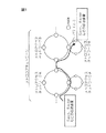
図1は、メトロリングネットワークの一例を示したものである。
従来からビル間をまたぐ企業内LAN同士や近郊都市間を結ぶメトロ向けシステムではリングネットワークが指向されている。メトロ領域は、図1に示すように市街地域内でのビル間接続のように加入者側に近いメトロアクセスネットワーク (Metro Access Network) A、Bで構成される領域と、近郊都市のメトロアクセスネットワーク同士を接続したり、長距離ネットワークに接続するメトロコアネットワーク (Metro Core Network; Metro IOF (interoffice)とも呼ぶ)で構成される領域とに分けられる。
【0004】
現在ではメトロアクセスネットワーク向けにもWDMが適用されており、そこではパッシブOADM (Passive Optical Add Drop Multiplexing) 方式が主流となっている。
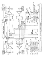
図2には、パッシブOADM方式によるメトロアクセスネットワークの一例を示している。図2の(a)は4つのノードA〜Dで構成された2ファイバリングネットワークの例を示しており、図2の(b)には各ノードA〜Dにおける片方向の装置内構成の例を示している。
【0005】
図2の(b)において、いずれか一方向のファイバ10上に伝送される32波長(λ1〜λ32)のWDM信号のうち、波長λ1〜λ3の帯域信号が誘電体多層膜フィルタ等の波長固定フィルタ11によってドロップ (Drop) され、それらは次段の光分波器12によってさらに各波長毎の光信号λ1〜λ3に分離される。各波長信号λ1〜λ3は、対応するトランスポンダ13〜15によって光増幅や波長変換等の処理がなされた後、そのノードが収容するルータ等の外部ネットワーク機器に出力される。
【0006】
一方、外部ネットワークから入力される信号は、各トランスポンダ23〜25によって対応する各波長信号λ4〜λ6に変換される。それらは波長固定フィルタ21を介して、合波器22により結合された波長λ4〜λ6の信号としてファイバ10上に伝送される32波長(λ1〜λ32)のWDM信号にアッド (Add) される。
【0007】
このように、パッシブOADM方式によれば、特定の波長や波長群の光信号を容易にWDM信号からアッドしたりドロップしたりすることができる。しかしながら、各ノードは自装置用に調整された波長固定フィルタ11及び21等の専用部品を使用するため、各ノードに割り当てられる信号パスのルート(使用波長又は波長群)は固定化される。
【0008】
その結果、パッシブOADM方式によるネットワーク設計では、事前にノード間の伝送ルートや伝送容量を決定し、そのためのフィルタを配置する必要がある。また、事後的に伝送ルートや伝送容量の変更が生じた場合は、一度ネットワークを切断してサービスを終了し、それに対応するフィルタを追加する必要がある。
【0009】
今後はアクセスネットワークと長距離ネットワークとの間に位置するメトロコアネットワーク向けにWDMを用いた光リングネットワークの導入が進んでいくものと考えられる。図1に示すようにメトロコアネットワークもプロテクション技術の容易性からその基本はリング構成であり、それを多段に接続することで大規模なネットワークを構築する。また、空きノードで図2に示すパッシブOADM方式のようなメトロアクセスネットワークのリングと接続したり、長距離ネットワークと接続を行なう。
【0010】
この場合、アクセス網から集線してきたデータ信号をノード間で交換したり、長距離網へ接続するのに回線を大容量化したり、回線ルートの切替える技術が重要となる。以下の3つの理由から、パス(回線ルート)の変更頻度は今後一層高くなり、その変更を自動的に行なうことは必須である。
【0011】
(1)ネットワーク規模及び需要の増大により回線ルートの設定変更がより頻繁に発生する。(2)IP over WDMの提供のためにWDMシステム側でプロテクション機能を提供する。この場合、ビットレート無依存性から光レイヤ層で波長切替えを行い、SONET (Synchronous Optical Network) リングに準じた短時間内(50〜100ms)でその切替えを完了する必要がある。(3)将来、波長の時間貸しサービスの提供により回線ルートの変更頻度が増加する。この場合もその切替えを上記短時間内で行なう必要がある。
【0012】
上述したことから、メトロアクセスネットワークの伝送ルートや伝送容量の変更によるネットワークの切断やサービス停止等に柔軟に対処し、誤接続を防止しながら接続先の遠隔切替えを実行する機能をサポートする必要がある。
【0013】
図3は、BPSR (Bi-directional Path Shared Ring) 方式によるパスプロテクション機能を備えたリングネットワークの動作を図式的に説明したものである。
図3では、2ファイバリングの1つのファイバ上に信号を時計回りに及び別のファイバ上に信号を反時計回りに伝送する。ここでは、各々のファイバ上に伝送される波長信号群をワーク (Work) 信号とプロテクション (protection) 信号とに分ける。例えば、時計回りの波長信号群はその偶数波長をワーク信号用に、そして奇数波長をプロテクション信号用に割り当てる。一方、反時計回りの波長信号群はその奇数波長をワーク信号用に、そして偶数波長をプロテクション信号用に割り当てる。
【0014】
正常通信時において、送信端ノードAは受信端ノードDに対してワーク信号を使用して図中に実線で示す時計回りのワークパス (Work Path;λx) 上に信号を送信する。受信端ノードDでは、ワークパス側を選択してその信号を受信する。一方、図中に点線で示す反時計回りのそのプロテクションパス(Protection Path;λx) は空き状態である。
【0015】
ここで、ワークパス側に断線等の回線障害が発生すると、送信端ノードAがプロテクションパス側にパスを切替えて信号の送信を継続する。以降、受信端ノードDもプロテクションパス側に切替えて信号の受信を継続する。なお、回線障害等により遮断された信号はプロテクション動作によって50〜100ms以内に復旧させる必要がある。
【0016】
ところで、通常はプロテクション用のルートに優先度の低い信号PCA (Protection Channel Access) パスを適当に張ってパスの共有化を図り、その運用効率を高めることが行なわれる。この場合には、ワーク側の障害発生時にプロテクション側のPCA信号を終了して、優先度の高いプロテクション信号を挿入する。
回線ルートの設定切替えは、回線ルートの障害発生時に限らず波長の時間貸しサービス等のように回線正常時においても頻繁に発生する。
【0017】
【発明が解決しようとする課題】
上述した回線ルートの設定切替えは、ネットワークマネージメントシステムがその切替え手順及び切替えタイミングを適切に管理して指示する必要があるが、従来においては以下に示すように、回線ルートの設定切替え時にパスの誤接続が発生するという問題や、それを防止するための指示系統の処理遅延という問題が生じていた。
【0018】
図4は、プロテクション動作時に発生する誤接続の一例を示している。
図4の(a)は、正常な通信状態を示している。ここで、送信端ノードDからは受信端ノードBへはワークパスλ1を介して反時計回りの信号を送信し、また送信端ノードAからは受信端ノードCへそのプロテクションパスλ1を使用してより優先度の低いPCA信号を時計回りに送信している。
【0019】
図4の(b)には、ノードCとノードDとの間のワークパスλ1にファイバ切断等の回線障害が発生した場合を示している。この場合、プロテクション動作によってプロテクションパスλ1の側へ回線ルートが切替えられる。その結果、送信端ノードDからの信号はノードAを中継して受信端ノードBへ時計回りに送信される。中継ノードAは自身のPCA信号の送信を終了して送信端ノードDからの信号をスルーさせ、また受信端ノードBはプロテクションパスλ1の側から信号を受信するように受信ルートを切替える。
【0020】
上記の場合、各ノードA〜Dの間における相対的な回線ルートの切替えタイミング、すなわちその切替え順序が問題となる。受信端ノードBから切替えを開始する場合には、ノードBで時計回りのルートをスルーからドロップに切替えた後、中継ノードAがPCA信号の送信を終了してスルーに切替えるまでの間はノードAからのPCA信号が受信端ノードBに誤接続されて外部ネットワークへ出力される。
【0021】
反対に送信端ノードDから切替えを開始する場合は、先ず送信端ノードDが時計回りのルートに回線ルートを切替えて信号を送信する。その後、中継ノードAがPCA信号の送信を終了してスルーに切替えてから受信端ノードBが時計回りのルートをスルーからドロップに切替えるまでの間、送信端ノードDからの信号はPCA信号の受信端ノードであるノードCに誤接続されて外部ネットワークへ出力される。
【0022】
図5には、上述した誤接続の動作をより具体的に説明するため、ノード構成の一例を示している。
先ず、図5のノード構成について簡単に説明しておく。時計回りルートの光ファイバ31から入力されるWDM信号は、光プリアンプ37によって増幅された後、光分波器38によって各波長信号(λ1〜λn)に分離されて出力される。また、その入力信号の一部は光分波器32により光監視部(OSC;Optical Supervisory Channel)33に入力される。
【0023】
光監視部33では、入力信号を電気信号に変換して次段の処理部/制御部34に与える。処理部/制御部34では入力信号等により時計回りルートの光ファイバ31の通信状態を確認し、障害発生時にはノード内部のスイッチ制御等を行なう。また、次段のノードに与えるパイロット信号等は出力側の光監視部35及び光合波部36を介して出力される。
【0024】
次に、ノード内部のスイッチ動作について説明すると、光分波器38で分離された時計回りのワーク信号λ1(w)は2×2光スイッチ39に入力される。2×2光スイッチ39がアッド/ドロップ設定であれば、入力されたワーク信号λ1(w)をドロップし、次段の光カプラ45及び冗長構成をとるトランスポンダ47又は48を介して外部ネットワーク59へ出力する。
【0025】
また、外部ネットワーク59からの信号は冗長構成をとるトランスポンダ51又は52、及び1×2光スイッチ50を介して2×2光スイッチ39に入力され、2×2光スイッチ39はそれをアッドして次段の光減衰器40、光合波器41、光ポストアンプ42、及び光合波器36を介して時計回りルートの光ファイバ31へWDM信号の1波として出力する。
【0026】
一方、2×2光スイッチ39がスルー設定であれば、入力されたワーク信号λ1(w)をスルーして次段の光減衰器40、光合波器41、光ポストアンプ42、及び光合波器36を介して時計回りルートの光ファイバ31へWDM信号の1波として出力する。同様の処理は、反時計回りルートの光ファイバ43から入力されるそのプロテクション信号λ1(p)に対しても2×2光スイッチ44によりなされる。
【0027】
なお、図中の下部中央には、外部ネットワーク59とのインタフェースに光信号を一度電気信号に変換した後に所定の光信号へ変換するトランスポンダタイプではなく、2×2光スイッチと外部ネットワーク59との間を直接接続する直接接続タイプも示している。この場合にはリング外のネットワーク機器にWDM用の光送信機/受信器が組み込まれる。
【0028】
次に、上述したノード構成を前提に、図4の誤接続動作についてより具体的に説明する。ノードCとノードDとの間で発生した回線障害により、受信端ノードBから2×2光スイッチ44をスルーからアッド/ドロップに設定して光カプラ46の側をオンに切替えると、中継ノードAが2×2光スイッチ44をアッド/ドロップ設定からスルー設定に切替えるまでの間、ノードAからのPCA信号がノードBの外部ネットワーク59へ出力される。
【0029】
一方、送信端ノードDが2×2光スイッチ44をアッド/ドロップに設定して1×2光スイッチ49の側をオンに切替えて時計回りの回線ルートの送信を開始して、次に中継ノードAが2×2光スイッチ44をアッド/ドロップからスルー設定に切替えると、受信端ノードBが2×2光スイッチ44をスルーからアッド/ドロップに設定するまでの間、ノードDからの信号がノードCの外部ネットワーク59へ出力される。
【0030】
さらに、上述した誤接続を防止するためにネットワークマネージメント側から個々のノードに切替え手順を指示するとネットワークマネージメント側の負荷が過大となり、またノード全体で回線ルートの切替えに要する時間が長くなるという問題があった。
【0031】
そこで本発明の目的は、上記問題点に鑑み、回線ルートの切替え設定時にノードのドロップパスから外部ネットワークへの誤接続を防止するWDMリングネットワークシステムを提供することにある。
また、本発明の目的は、パス切替えに関して迅速なネットワークマネージメント管理や指示を可能とし、大規模化するリングネットワークシステムに要求される通信品質を満足するWDMリングネットワークシステムを提供することにある。
【0032】
これにより、メトロコアリングネットワーク等の大規模なWDMリングネットワークシステムに対して、回線ルート切替え時の誤接続の防止、及び従来のSONETリングがサポートしていたプロテクション機能や波長の時間貸しサービスによる接続先の遠隔切替え機能、等のサポートが可能となる。
【0033】
【課題を解決するための手段】
本発明によれば、光ネットワークの所定の光パスに接続される光通信ノードであって、前記光通信ノードはその配下に収容する外部ネットワークと、前記光ネットワークと前記外部ネットワークと間の接続を遮断する遮断手段と、を有し、前記遮断手段は、前記光パスのルート設定変更時に、前記光パスのルート設定変更に関して誤接続が一時的に発生し得るとき、そのルート変更のシーケンスの完了までは遮断される光通信ノードが提供される。
【0034】
前記遮断手段は、さらに他の光通信ノードからの指示により遮断され、又はその遮断が解除される。前記光通信ノードは、さらに送信信号に受信端ノード識別子を付加する付加手段と受信信号に含まれる前記受信端ノード識別子を検出する検出手段とを有し、前記検出手段は自ノードの前記受信端ノード識別子を検出すると、前記遮断手段による遮断を解除する。
【0035】
前記光通信ノードは、さらにダミー信号を生成出力するダミー信号手段を有し、前記遮断手段により信号の送信が停止される前記光パス及び/又は前記外部ネットワークに対して、前記ダミー信号手段によるダミー信号が送出される。
【0036】
また本発明によれば、光パスのルート設定変更時に、前記光パスのルート設定変更に関して誤接続が一時的に発生し得るとき、ルート変更のシーケンスの完了までの間、外部光ネットワークから該光ネットワークへの入力側へ又は該光ネットワークから外部光ネットワークの出力側への少なくとも一方の信号を遮断する光ネットワークシステムが提供される。
【0037】
【発明の実施の形態】
図6は、本発明の第1の実施例を示したものである。
図6では、障害発生時に切替えられる回線ルート上の各ノードD、A、及びBに外部に信号が出力されるのを防止するための遮断手段63、62及び61をそれぞれ設ける。
【0038】
図7には、本発明の第1の実施例における回線切替えシーケンスの一例を示している。本例では、最初に障害を検出する下流側の受信端ノードBの側から回線切替えシーケンスが開始される。
図7において、ステップS101では、受信端ノードBがワーク信号λ1(w)の信号異常を検出すると、遮断手段61によってそのワーク信号λ1(w)及びプロテクション信号λ1(p)の双方とも各々のドロップパスから外部ネットワーク59への出力が遮断される。この場合、ノードBから外部ネットワーク59へはAIS(Alarm Indication Signal)信号等のダミー信号が出力されるか、もしくは信号を出力しない。
【0039】
次に、回線ルートをワーク側からプロテクション側へ切替えて装置内の方路をスルーからアッド/ドロップ設定に切替える。これにより、以降の処理におけるノードC側への誤接続が防止される。その後、プロテクション側の回線ルート上に存在する上流の各中継ノード(本例ではノードA)に対して切替え信号を送信し、送信端ノードDにはスイッチ切替え制御信号であるAPS(Auto Protection Switching)信号を送信する。ここで、各ノード間でのパス切替えに関する信号の送受信には監視制御信号(OSC)が用いられる。
【0040】
ステップS102では、各中継ノードが受信した切替え信号により、必要なら装置内の方路を切替える。その際、ノードAは遮断手段62によって外部ネットワーク59との間の接続を一時的に遮断して装置内部の方路切替え時における信号漏れを回避する。本例では中継ノードAが時計回りのルートをアッド/ドロップからスルー設定に変更する。そして、その旨を送信元のノードBに通知する。
【0041】
ステップS103では、送信端ノードDがAPS信号を受信すると、ノードDは遮断手段63によって外部ネットワーク59との間の接続を一時的に遮断して装置内部の方路切替え時における信号漏れを回避する。次に、信号の送信ルートをワーク側の反時計回りルートからプロテクション側の時計回りルートへ切替える。そして、その時計回りルートをアッド/ドロップに設定する。
【0042】
ステップS104では、送信端ノードDがパス設定完了を受信端ノードBへ通知する。ステップS105では、受信端ノードBが各中継ノード(本例では中継ノードA)からの正常切替え信号と送信端ノードDからのパス設定完了信号との受信を確認した後に、前記遮断手段61を開放して波長λ1のプロテクション信号λ1(p)がドロップパスから外部ネットワーク59へ出力するのを許可する。上述したように、本例では受信端ノードBにおける遮断手段61が誤接続防止のための主要な役割を果たすことになる。
【0043】
図8は、第1の実施例の具体的な回路構成例(1)を示したものである。
図8において、光信号の監視制御部には、従来の入力側の光監視部33、処理部/制御部34及び出力側の光監視部35に加えて、上流の監視制御部からの監視制御信号を通じた切替え制御信号に基づいて本発明の遮断手段を制御する制御部71が新たに設けられている。
【0044】
また、ドロップ側のトランスポンダ47及び48には、新たにAIS発生部72と本願発明の遮断手段を構成する切替え部73とが設けられている。AIS発生部72は、“1”及び“0”値の交番パターンからなるダミー信号を発生し、また切替え部73は従来の信号処理部又はAIS発生部72からのいずれかの信号を選択して外部ネットワーク59に出力する。ここで、切替え部73によってAIS発生部72側が選択されると外部ネットワーク59に対して遮断状態となる。
【0045】
第1の実施例の動作で説明すると、反時計回りの回線ルートに障害が発生すると、受信端ノードBの信号処理部34がそれを検出して制御部71が切替え部73を制御してAIS発生部72側を選択する。次に、トランスポンダ内の1×2光スイッチ53を制御して、ワーク側の2×2光スイッチ44からドロップする信号をプロテクション側の2×2光スイッチ39からドロップする信号に切替える。
【0046】
図9は、第1の実施例における別の回路構成例(2)を示したものである。
図9には、図8のAIS発生部72及び切替え部73を含むトランスポンダに代えて、光信号の通過/遮断のみを制御する簡易なシャッタカード74及び75を使用している。本例ではシャッタカードを使用することで図5の直接接続形態にも本願発明を適用可能としている。
【0047】
シャッタカード74内の1×2光スイッチ又は光減衰器部77が制御部71によって外部ネットワーク59との間の信号を遮断する。なお、1×2光スイッチ77の一方にAIS信号を発生する送信器を接続することで、遮断時にはダミー信号を外部ネットワーク59に出力させることもできる。第1の実施例の動作は図8と同様である。
【0048】
図10は、本発明の第2の実施例を示したものである。
図11には、本発明の第2の実施例における回線切替えシーケンスの一例を示している。本例では、所定のルート設定が完了するまでの間、ルート切替え区間を通過する切替え対象波長について送信端ノードが信号出力を停止する。
【0049】
図11において、ステップS201では、受信端ノードBがワーク信号λ1(w)の信号異常を検出すると、不要な信号漏れを防止するために遮断手段61によってそのワーク信号λ1(w)及びプロテクション信号λ1(p)の双方とも各々のドロップパスから外部ネットワーク59への出力が遮断される。この場合、ノードBから外部ネットワーク59へはAIS信号等のダミー信号が出力される。
【0050】
なお、遮断手段61によって信号λ1を外部ネットワーク59と遮断することは本例において必須事項ではない。次に、ノードBでドロップする信号の送信端ノード及びノードBを通過する信号の送信端ノードへ送信停止要求を送出する。本例では、送信端ノードD及びAに対して送信停止要求がなされる。各ノード間における制御信号の送受信には監視制御信号(OSC)が用いられる。
【0051】
ステップS202では、送信端ノードD及び受信端ノードBと送信端ノードDとの間にあってAPS信号を送信している中継ノードAが前記送信停止要求を受信する。ノードD及びAはそれぞれの遮断手段63及び62によって自ノードからの送信光を遮断するか又はそれに代えてダミー信号を送信する。その後、ノードD及びAは送信停止完了を受信端ノードBへ通知する。
【0052】
また、図10には示していないが、送信停止要求を受信したノードD及びAがさらに自ノード内でドロップするか又は自ノードを通過する信号を送信する別の送信端ノードを有する場合には、上記と同様の手順によりノードD及びAが別のノードに対して送信停止要求を送出して信号送信停止の完了通知を受信する。この場合、ノードD及びAが別のノードから送信停止完了の通知を受信してから前記ノードD及びAにおける送信停止完了を受信端ノードBへ通知する。
【0053】
ステップS203では、中継ノードA及び送信端ノードDから送信停止完了通知を受信した受信端ノードBが自ノード内のルート切替えを行い、且つノードA及びDに順次ルート切替えを指示する。本例では、送信信号の存在しない回線ルート上で各ノードA、B及びDがルート切替えを実行するため、当然にルート切替え時の誤接続は発生しない。
【0054】
ステップS204及び205では、中継ノードA及び送信端ノードDからルート切替えの完了を受信したノードBは、自ノードの遮断手段61を解除し、且つノードA及びDに送信停止要求の解除を通知する。その結果、ノードA及びDの遮断手段63及び62は解除され、送信端ノードDによる信号の送信が開始される。上述したように、本例では送信端ノードD及びAにおける遮断手段63及び62が誤接続防止のための主要な役割を果たすことになる。
【0055】
図12は、第2の実施例の具体的な回路構成例(1)を示したものである。
図12において、光信号の監視制御部については図8及び9と同じである。本実施例ではアッド側のトランスポンダ50及び52に、新たにAIS発生部72と本願発明の遮断手段を構成する切替え部73とが設けられている。また、切替え部73は信号処理部又はAIS発生部72のいずれかを選択したアッド信号を出力する。ここで、切替え部73によってAIS発生部72側が選択されると遮断状態となる。
【0056】
第2の実施例の動作で説明すると、反時計回りの回線ルートに障害が発生すると、受信端ノードBの信号処理部34がそれを検出してAPS信号を送信端ノードDに通知する。送信端ノードDの信号処理部34がそれを検出し、制御部71が切替え部73を制御してAIS発生部72からのダミー信号を出力させる。次に、プロテクション側の2×2光スイッチ39はアッド/ドロップ設定に切替えられ、前記ダミー信号がアッド信号として入力される。
【0057】
図13は、第2の実施例における別の回路構成例(2)を示したものである。図13は、先に説明した図9と同様に、アッド側のトランスポンダ50及び52が光信号の通過/遮断のみを制御する簡易なシャッタカード80及び81に置き換えられただけであり、シャッタカード内の1×2光スイッチ又は光減衰器部82も図9のものと同様である。本例ではシャッタカードを使用することで図5の直接接続形態にも本願発明を適用可能としており、本例の動作は図12と同様である。
【0058】
図14は、本発明の第3の実施例を示したものである。
上述した第1及び第2の実施例では、ルート切替えの制御信号として監視制御信号(OSC)が用いられ、各ノード間で個別に制御信号を送受信することによって各ノード内の遮断手段61〜63や方路スイッチの制御を行なっている。従って、第1及び第2の実施例によって誤接続の問題は解消するが、ネットワーク規模が大きくなったり複数のリングネットワーク間にまたがるパス設定がなされるような場合には、回線ルートの切替え時間が増大して通信品質が低下する恐れがある。
【0059】
本実施例は、この点を解消すべく本発明による遮断手段61〜63の制御を簡易且つ高速に実行できるようにする。そのため、各ノード毎に所定の識別子を定めておき、送信端ノードでは送信信号内にその識別子含めて送信する。受信端ノードでは受信信号に含まれる識別子を解読し、自ノード宛なら遮断手段を解除してそのドロップパスを外部ネットワーク59に接続する。反対に、自ノード宛でない場合は遮断手段によって外部ネットワークとの間の接続を遮断する。
【0060】
図15には、デジタルラッパを使用する信号フォーマットの一例を示している。ここではOTU (Optical channel Transport Unit)kフレーム構成を使用しており、そのヘッダ部のSAPI (Source Access Point Identifier) 及びDAPI (Destination Access Point Identifier) の各ロケーションに本願発明の受信端識別子を設定し、そのデータ信号部に送信信号を挿入して送信する。
【0061】
例えば、トランスポンダを用いる場合には、送信側のトランスポンダでデジタルラッパ符号化を行って前記ヘッダ部に受信端ノードの識別子を設定する。受信側のトランスポンダではデジタルラッパ復号化を行い、自ノード宛の場合は受信信号を外部ネットワーク59に出力する。自ノード以外の場合は、その出力を遮断するかダミー信号を出力する。
【0062】
また、デジタルラッパ以外の他の方法として、送信端ノードや受信端ノードでトランスポンダを用いる場合に、受信端ノード毎に信号処理部で施すデスクランブルパターンを固有のパターンとして割り当て、これを前記受信端識別子として使用する。この場合、送信端ノードの信号処理部で施すスクランブルパターンを受信端ノードのスクランブルパターンとすることで、上記デジタルラッパよりも簡易な手法で同様の処理が可能となる。
【0063】
ところで、リタイミング゛を行なわない2Rトランスポンダ゛を用いる場合や、外部ネットワーク59におけるネットワーク機器側にWDMインタフェースが備えられてトランスポンダを介さずに直接リングネットワークに接続する場合(直接接続形態)には、上記デジタルラッパ化等によるデータ信号自体を操作することができない。本発明では、このような場合にも送信信号に受信端識別情報を付加するために、低速のパイロット信号を主信号に振幅変調(AM)や位相変調(PSK)等により重畳して送信する。
【0064】
図16は、第3の実施例における送信端ノード側の具体的な回路構成例(1)を示したものである。
本実施例のアッド側のトランスポンダ51及び52には、従来のものに新たにパイロット信号送信部85が付加されている。パイロット信号送信部85は、図15のデジタルラッパ信号に代えて、受信端識別子の情報をAMやPSK等の所定の低速変調信号(パイロット信号)として送信信号に付加し、その変調された送信信号を生成して送信する。なお、先に説明した第1及び第2の実施例における光信号の監視制御部は本実施例の動作に直接関与しないため示されていない。
【0065】
図20には、パイロット送信部の一構成例を示している。相手先ノード(受信端ノード)の情報が入力される符号器92と低速度(f0)の発振器93により受信端識別情報を含む振幅変調信号が生成され、それを光変調器91によって送信信号に重畳する。光変調器は変調方式により選択され、例えば振幅変調信号を重畳する場合にはMZ干渉型の変調器や光アッテネータを用いる。なお、複数のリングを通過する場合には、各々のリング間のジャンクションでパイロット信号を一度終端し、再度次のリング内の終端ノードに割り振られたパイロット信号を重畳するようにしてもよい。
【0066】
第3の実施例の動作で説明すると、送信端ノードDは外部ネットワーク59からの送信信号に受信端ノードBの識別子情報を含むパイロット信号を付加した信号を送信する。本実施例では、前記パイロット信号が1×2光スイッチ49を介して2×2光スイッチ39にアッドされ、時計回りの回線ルートに出力される。
【0067】
図17は、第3の実施例における送信端ノード側の別の回路構成例(2)を示したものである。
図17では、トランスポンダの代わりにシャッタカード80及び81を使用する。ここでもパイロット信号送信部85が設けられるが、その動作は図16のものと同じである。本構成は図5の直接接続形態に適した構成である。
【0068】
図18は、第3の実施例における受信端ノード側の具体的な回路構成例(1)を示したものである。
本実施例のドロップ側のトランスポンダ47及び48には、AIS発生部72と本願発明の遮断手段を構成する切替え部73とが設けられているが、本例ではさらに切替え部73を制御するパイロット信号受信部84が設けられている。パイロット信号受信部84は、受信信号に付加されたパイロット信号(変調信号)を復号し、そこに含まれる受信端識別子の情報が自ノードである場合に切替え部73を制御して信号処理部側を選択する。その結果、遮断状態が解除される。反対に、自ノード以外の場合はAIS発生部72側を選択して遮断状態とするかその状態を維持する。
【0069】
図21には、パイロット信号受信部84の一構成例を示している。
図21において、入力信号の一部はカプラ等の分岐手段94によって分岐されてフォトダイオード(PD)95により検出される。その検出信号と送信側と同じ周波数(f0)を有する発振器96からの局部発振周波信号とを混合器97で混合された信号は復号器98で着信先ノード情報(受信端識別子)に復号される。制御回路99は、その復号値と自ノードの識別子とを比較して、それらが一致した場合には切替え部73を制御して遮断状態を解除する。
【0070】
第3の実施例の動作で説明すると、受信端ノードBは、時計回りの回線ルートの2×2光スイッチ39からのドロップ信号に含まれるパイロット信号を、トランスポンダ内のパイロット信号受信部84で復調する。その復調結果から、受信端識別子の情報が自ノードBあての信号であることを認識して、信号処理部側を選択するように切替え部73を制御する。なお、中継ノードAにおいては、前記復調結果が自ノード宛でないため、パイロット信号受信部84がAIS発生部72側を選択するように切替え部73を制御する。
【0071】
図19は、第3の実施例における受信端ノード側の別の回路構成例(2)を示したものである。
図19では、トランスポンダの代わりにシャッタカード74及び75を使用する。ここでもパイロット信号送信部85が設けられるが、パイロット信号送信部85が1×2光スイッチ又は光減衰器部77によって外部ネットワーク59との間の信号を遮断制御する以外は、図18と同様である。本例の第3の実施例における動作は図18と同様である。本構成は図5の直接接続形態に適した構成である。
【0072】
なお、これまで述べた第1〜3の実施例をリングネットワーク同士の接続に適用する場合、各実施例に基づき各々のリングネットワークで独立にパスの切替えシーケンスを実行すればよい。
【0073】
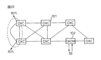
図22〜24は、光クロスコネクト(OXC)装置によって構成したメッシュネットワークに本願発明を適用した実施例を示している。
図22には光クロスコネクト装置101によって構成したメッシュネットワークの一例を、図23には障害発生時におけるメッシュネットワークの回線ルート切替えの一例を、そして図24には光クロスコネクト装置101の一構成例をそれぞれ示している。
【0074】
図22に示すメッシュネットワークでは、ファイバの切断時や装置故障時に迂回用のパスルートをデータベースにより検索してパスの切替えを行なう。その際、使用していない光パスや優先度の低い光パスの順で迂回ルートを検索する。なお、図中には示されていないが光クロスコネクト装置101間には光中継器として光アンプがはいる場合がある。また、図中の光ADM(OADM)装置102は外部ネットワーク59との接続に使用される。
【0075】
図24に示す光クロスコネクト装置101の内部のスイッチ部(switch)111は光マトリクススイッチであり、カプラ113で分岐する1+1の冗長構成をとっている。また、図中にトランスポンダ112及び114を記載しているが、トランスポンダ112及び114の代わりにシャッタカードを用いる場合もある。さらに、シャッタカードも用意せずにシャッタカードの機能を前記スイッチ部111で代用することもできる。
【0076】
図23には4つの光クロスコネクト装置101がそれぞれノードA〜Dとして論理的なリングノードを形成している。これに本願発明を適用するに際し、先ず第1の実施例に準じる場合から説明する。ファイバの切断や装置故障等によりノードCとノードDとの間に障害が発生すると、受信端ノードCにおいて切替えるパスの下流への接続をまず遮断する。次に、上流側のノードB及びAへ接続を切替えていく。そして、最上流のノードDまで切替えを実行し、すべての切替えが終了した後に受信端ノードCにおける下流への接続を開放する。
【0077】
遮断方法は、図24のトランスポンダ114か、又はトランスポンダ114の代わりに図9の示すシャッタカード74に相当するものを使って実現する。他には、マトリックススイッチ部111で接続のないポートと結合すれば同様の遮断を実現できる。上述したことは、本願発明の第2の実施例に準じる場合にも同様に適用可能である。
【0078】
本願発明の第3の実施例に準じる場合、先に述べたように信号内に識別子を入れる手法とパイロット信号を用いる手法がある。先ず、信号内に識別子を入れる場合について説明する。本例では、送信端ノードDの局内インタフェースの送信側で受信端ノードCの所定ポートの局内インタフェースに対応する識別子を挿入する。受信端ノードC内の局内インタフェースの受信側で自ノードの識別子を検出すると、外部のネットワークへ出力する。また、送信信号にそれが経由するノード情報を含めてもよく、中継ノードでその異常を検出した場合にはそのノードで遮断するようにしてもよい。
【0079】
一方、パイロット信号を用いる場合には、送信端ノードDの局内インタフェースの送信側には先に説明したトランスポンダ又は直接接続の各形態である図16又は17の構成を、また受信端ノードCの局内インタフェースの受信側にも図17又は18の構成を用いることができる。受信端ノードCで受信端識別情報を含む所定のデータ信号がこなければ外部のネットワークへの出力を遮断する。
【0080】
【発明の効果】
以上説明したように、本発明によれば誤接続が発生することなく高速のルート切替えが可能なWDMネットワークが提供される。これにより、メトロコアリングネットワーク等に対して、回線ルート切替え時の誤接続の防止、及び波長の時間貸しサービスによる接続先の遠隔切替え機能、等が提供可能となる。
【図面の簡単な説明】
【図1】メトロリングネットワークの一例を示した図である。
【図2】パッシブOADM方式によるメトロアクセスネットワークの一例を示した図である。
【図3】BPSR方式によるパスプロテクション機能を備えたリングネットワークの動作を図式的に説明した図である。
【図4】プロテクション動作時に発生する誤接続の一例を示した図である。
【図5】リングノード構成の一例を示した図である。
【図6】本発明の第1の実施例を示したものである。
【図7】本発明の第1の実施例における回線切替えシーケンス例を示した図である。
【図8】第1の実施例の具体的な回路構成例(1)を示した図である。
【図9】第1の実施例における別の回路構成例(2)を示した図である。
【図10】本発明の第2の実施例を示した図である。
【図11】本発明の第2の実施例における回線切替えシーケンス例を示した図である。
【図12】第2の実施例の具体的な回路構成例(1)を示した図である。
【図13】第2の実施例における別の回路構成例(2)を示した図である。
【図14】本発明の第3の実施例を示した図である。
【図15】デジタルラッパを使用する信号フォーマットの一例を示した図である。
【図16】第3の実施例における送信端ノード側の具体的な回路構成例(1)を示した図である。
【図17】第3の実施例における送信端ノード側の別の回路構成例(2)を示した図である。
【図18】第3の実施例における受信端ノード側の具体的な回路構成例(1)を示した図である。
【図19】第3の実施例における受信端ノード側の別の回路構成例(2)を示した図である。
【図20】パイロット送信部の一構成例を示した図である。
【図21】パイロット信号受信部の一構成例を示した図である。
【図22】光クロスコネクト装置により構成したメッシュネットワークの一例を示した図である。
【図23】障害発生時におけるメッシュネットワークの回線ルート切替えの一例を示した図である。
【図24】光クロスコネクト装置の一構成例を示した図である。
【符号の説明】
10、31,43…ファイバ
11、21…光フィルタ
12、32、38…光分波器
22、41、36…光合波器
33、35…光監視制御装置
37、42…光アンプ
40…光減衰器
39、44,53、49、50、76、111…光スイッチ
47、48、51、52、112,114…トランスポンダ
59…外部ネットワーク
61〜63…遮断手段
71…制御部
72…AIS発生部
73…切替え部
74、75、80、81…シャッタカード
77、82…光スイッチ又は光可変減衰器
84…パイロット信号受信部
85…パイロット信号送信部
95…フォトダイオード
101…光クロスコネクト装置
102…光ADM装置[0001]
BACKGROUND OF THE INVENTION
The present invention relates to an optical communication node and an optical network, and more particularly to prevention of erroneous connection of an optical communication node and an optical network having a route switching function in a wavelength division multiplexing (WDM) network system.
[0002]
[Prior art]
In recent years, WDM systems suitable for large-capacity high-speed data transmission using optical signals have been introduced in accordance with the spread of Internet communication and image transmission. The introduction of the WDM system was first started from a long-distance network with great economic merit. Eventually, the maturity of the technology lowered the installation cost, and now the introduction of the WDM system is also being promoted in urban coring.
[0003]
FIG. 1 shows an example of a metro ring network.
Conventionally, a ring network is oriented to a system for a metro that connects corporate LANs that cross between buildings and between neighboring cities. As shown in Fig. 1, the metro area consists of metro access networks A and B that are close to the subscriber side, such as inter-building connections in urban areas, and metro access networks in suburban cities. Or an area composed of Metro Core Network (also called Metro IOF (interoffice)) that connects to long-distance networks.
[0004]
Currently, WDM is also applied to metro access networks, in which passive OADM (Passive Optical Add Drop Multiplexing) is the mainstream.
FIG. 2 shows an example of a metro access network based on the passive OADM system. FIG. 2A shows an example of a two-fiber ring network composed of four nodes A to D, and FIG. 2B shows an example of a one-way internal configuration in each node A to D. Is shown.
[0005]
In FIG. 2B, 32 wavelengths (λ) transmitted on the
[0006]
On the other hand, a signal input from an external network is transmitted by each transponder 23-25 to each corresponding wavelength signal λ. 4 ~ Λ 6 Is converted to The wavelength λ is coupled by the
[0007]
Thus, according to the passive OADM system, an optical signal having a specific wavelength or wavelength group can be easily added or dropped from the WDM signal. However, since each node uses dedicated components such as the wavelength
[0008]
As a result, in the network design based on the passive OADM method, it is necessary to determine the transmission route and transmission capacity between nodes in advance and arrange a filter for this purpose. Further, when the transmission route or the transmission capacity is changed after the fact, it is necessary to disconnect the network once to terminate the service and add a filter corresponding to it.
[0009]
In the future, it is considered that the introduction of an optical ring network using WDM for the metro core network located between the access network and the long-distance network will progress. As shown in FIG. 1, the metro core network is basically a ring configuration because of the ease of protection technology, and a large-scale network is constructed by connecting it in multiple stages. Further, a free node connects to a ring of a metro access network such as the passive OADM system shown in FIG. 2 or connects to a long distance network.
[0010]
In this case, techniques for exchanging data signals collected from the access network between nodes, increasing the capacity of the line, and switching the line route are important for connection to the long-distance network. For the following three reasons, the frequency of changing the path (line route) will become higher in the future, and it is essential to make the change automatically.
[0011]
(1) Line route setting changes occur more frequently due to an increase in network scale and demand. (2) To provide IP over WDM, a protection function is provided on the WDM system side. In this case, it is necessary to perform wavelength switching in the optical layer layer because of bit rate independence, and complete the switching within a short time (50 to 100 ms) in accordance with a SONET (Synchronous Optical Network) ring. (3) In the future, the frequency of line route changes will increase due to the provision of wavelength lending services. Also in this case, it is necessary to perform the switching within the short time.
[0012]
From the above, it is necessary to flexibly cope with network disconnection and service suspension due to changes in the transmission route and transmission capacity of the metro access network, and to support the function of performing remote switching of connection destinations while preventing erroneous connections. is there.
[0013]
FIG. 3 schematically illustrates the operation of a ring network having a path protection function based on the BPSR (Bi-directional Path Shared Ring) method.
In FIG. 3, a signal is transmitted clockwise on one fiber of a two-fiber ring and counterclockwise on another fiber. Here, a group of wavelength signals transmitted on each fiber is divided into a work signal and a protection signal. For example, a clockwise wavelength signal group assigns its even wavelengths for work signals and odd wavelengths for protection signals. On the other hand, the counterclockwise wavelength signal group assigns the odd wavelength to the work signal and the even wavelength to the protection signal.
[0014]
During normal communication, the transmitting end node A uses the work signal to the receiving end node D to use a work path (Work Path; λ x ) Send the signal up. The receiving end node D selects the work path side and receives the signal. On the other hand, the protection path (λ) is shown in the counterclockwise direction indicated by the dotted line in the figure. x ) Is empty.
[0015]
Here, when a line failure such as disconnection occurs on the work path side, the transmission end node A switches the path to the protection path side and continues signal transmission. Thereafter, the receiving end node D also switches to the protection path side and continues receiving signals. It should be noted that a signal cut off due to a line failure or the like needs to be restored within 50 to 100 ms by a protection operation.
[0016]
By the way, normally, a low-priority signal PCA (Protection Channel Access) path is appropriately placed on the protection route so as to share the path, thereby improving the operation efficiency. In this case, when a failure on the workpiece side occurs, the PCA signal on the protection side is terminated and a protection signal with a high priority is inserted.
Line route setting switching occurs frequently not only when a line route failure occurs but also when the line is normal, such as a wavelength lending service.
[0017]
[Problems to be solved by the invention]
The above-described line route setting switching requires the network management system to appropriately manage and instruct the switching procedure and switching timing. However, conventionally, as shown below, a path error occurs when the line route setting is switched. There has been a problem of connection and a problem of processing delay of an instruction system for preventing the connection.
[0018]
FIG. 4 shows an example of erroneous connection that occurs during the protection operation.
FIG. 4A shows a normal communication state. Here, the work path λ from the transmitting end node D to the receiving end node B 1 A counterclockwise signal is transmitted via the transmission end node A, and the protection path λ is transmitted from the transmission end node A to the reception end node C. 1 Is used to transmit a lower priority PCA signal clockwise.
[0019]
FIG. 4B shows a work path λ between the node C and the node D. 1 Shows a case where a line failure such as a fiber cut has occurred. In this case, the protection path λ 1 The line route is switched to the side. As a result, the signal from the transmission end node D is transmitted clockwise to the reception end node B via the node A. The relay node A terminates transmission of its own PCA signal and allows the signal from the transmission end node D to pass through, and the reception end node B transmits the protection path λ. 1 The reception route is switched so as to receive the signal from the side of the receiver.
[0020]
In the above case, the relative line route switching timing between the nodes A to D, that is, the switching order becomes a problem. When switching is started from the receiving end node B, after the clockwise route is switched from through to drop at the node B, the relay node A ends transmission of the PCA signal and switches to through until the node A is switched. The PCA signal from is erroneously connected to the receiving end node B and output to the external network.
[0021]
On the contrary, when switching is started from the transmission end node D, the transmission end node D first switches the line route to the clockwise route and transmits a signal. Thereafter, the signal from the transmitting end node D is received by the PCA signal until the receiving end node B switches the clockwise route from through to drop after the relay node A ends transmission of the PCA signal and switches to through. It is erroneously connected to node C, which is an end node, and output to the external network.
[0022]
FIG. 5 shows an example of a node configuration in order to more specifically describe the above-described erroneous connection operation.
First, the node configuration of FIG. 5 will be briefly described. The WDM signal input from the
[0023]
The
[0024]
Next, the switch operation inside the node will be described. The clockwise work signal λ separated by the optical demultiplexer 38 is described. 1 (W) is input to the 2 × 2
[0025]
The signal from the
[0026]
On the other hand, if the 2 × 2
[0027]
Note that the lower center in the figure is not a transponder type in which an optical signal is once converted into an electrical signal at an interface with the
[0028]
Next, the misconnection operation of FIG. 4 will be described more specifically on the premise of the node configuration described above. When the 2 × 2
[0029]
On the other hand, the transmitting end node D sets the 2 × 2
[0030]
Furthermore, in order to prevent the above-described erroneous connection, if the switching procedure is instructed from the network management side to each node, the load on the network management side becomes excessive, and the time required for switching the line route in the entire node becomes long. there were.
[0031]
In view of the above problems, an object of the present invention is to provide a WDM ring network system that prevents erroneous connection from a drop path of a node to an external network at the time of setting a line route switch.
It is another object of the present invention to provide a WDM ring network system that enables rapid network management management and instructions regarding path switching and satisfies the communication quality required for a ring network system that is becoming larger.
[0032]
As a result, connection to a large-scale WDM ring network system such as a metro core ring network can be prevented by using a protection function and a wavelength lending service that are supported by conventional SONET rings. Support for the remote switching function, etc. becomes possible.
[0033]
[Means for Solving the Problems]
According to the present invention, an optical communication node is connected to a predetermined optical path of an optical network, and the optical communication node connects an external network accommodated under the optical communication node and the connection between the optical network and the external network. And a blocking means for blocking, the blocking means, when changing the route setting of the optical path, When an erroneous connection may temporarily occur regarding the route setting change of the optical path, An optical communication node is provided that is blocked until completion of the route change sequence.
[0034]
The blocking means is blocked by an instruction from another optical communication node, or the blocking is released. The optical communication node further includes adding means for adding a receiving end node identifier to the transmission signal and detecting means for detecting the receiving end node identifier included in the received signal, and the detecting means is the receiving end of the own node. When the node identifier is detected, the blocking by the blocking means is released.
[0035]
The optical communication node further includes dummy signal means for generating and outputting a dummy signal, and the dummy signal means performs dummy processing with respect to the optical path and / or the external network in which signal transmission is stopped by the blocking means. A signal is sent out.
[0036]
According to the present invention, when the route setting of the optical path is changed, When an erroneous connection may temporarily occur regarding the route setting change of the optical path, An optical network system is provided that blocks at least one signal from an external optical network to an input side to the optical network or from the optical network to an output side of the external optical network until completion of a rerouting sequence.
[0037]
DETAILED DESCRIPTION OF THE INVENTION
FIG. 6 shows a first embodiment of the present invention.
In FIG. 6, blocking means 63, 62, and 61 are provided for preventing signals from being output to the nodes D, A, and B on the line route that are switched when a failure occurs.
[0038]
FIG. 7 shows an example of a line switching sequence in the first embodiment of the present invention. In this example, a line switching sequence is started from the downstream receiving end node B side that first detects a failure.
In FIG. 7, in step S101, the receiving end node B receives the work signal λ. 1 When the signal abnormality (w) is detected, the work signal λ is cut by the blocking means 61. 1 (W) and protection signal λ 1 In both cases (p), the output from each drop path to the
[0039]
Next, the line route is switched from the work side to the protection side, and the route in the apparatus is switched from through to add / drop setting. This prevents erroneous connection to the node C side in the subsequent processing. Thereafter, a switching signal is transmitted to each upstream relay node (node A in this example) existing on the protection-side circuit route, and APS (Auto Protection Switching) which is a switch switching control signal is transmitted to the transmitting end node D. Send a signal. Here, a supervisory control signal (OSC) is used for transmission and reception of signals related to path switching between the nodes.
[0040]
In step S102, the route in the apparatus is switched if necessary by the switching signal received by each relay node. At that time, the node A temporarily cuts off the connection with the
[0041]
In step S103, when the transmitting end node D receives the APS signal, the node D temporarily blocks the connection with the
[0042]
In step S104, the transmitting end node D notifies the receiving end node B of the completion of path setting. In step S105, the receiving end node B confirms the reception of the normal switching signal from each relay node (in this example, the relay node A) and the path setting completion signal from the transmitting end node D, and then opens the blocking means 61. Wavelength λ 1 Protection signal λ 1 (P) permits output from the drop path to the
[0043]
FIG. 8 shows a specific circuit configuration example (1) of the first embodiment.
In FIG. 8, the optical signal monitoring control unit includes monitoring control from an upstream monitoring control unit in addition to the conventional input side
[0044]
In addition, the
[0045]
In the operation of the first embodiment, when a failure occurs in the counterclockwise circuit route, the
[0046]
FIG. 9 shows another circuit configuration example (2) in the first embodiment.
In FIG. 9,
[0047]
The 1 × 2 optical switch or
[0048]
FIG. 10 shows a second embodiment of the present invention.
FIG. 11 shows an example of a line switching sequence in the second embodiment of the present invention. In this example, until the predetermined route setting is completed, the transmitting end node stops signal output for the switching target wavelength passing through the route switching section.
[0049]
In FIG. 11, in step S201, the receiving end node B receives the work signal λ. 1 When the signal abnormality of (w) is detected, the work signal λ is cut by the blocking means 61 in order to prevent unnecessary signal leakage. 1 (W) and protection signal λ 1 In both cases (p), the output from each drop path to the
[0050]
It should be noted that the signal λ is blocked by the blocking means 61 1 Is not essential in this example. Next, a transmission stop request is sent to the transmission end node of the signal dropped at Node B and the transmission end node of the signal passing through Node B. In this example, a transmission stop request is made to the transmitting end nodes D and A. A supervisory control signal (OSC) is used for transmission and reception of control signals between the nodes.
[0051]
In step S202, the relay node A that is between the transmitting end node D, the receiving end node B, and the transmitting end node D and is transmitting the APS signal receives the transmission stop request. The nodes D and A block the transmission light from their own nodes by the blocking means 63 and 62, or transmit dummy signals instead. Thereafter, the nodes D and A notify the reception end node B of the completion of transmission stop.
[0052]
Further, although not shown in FIG. 10, when the nodes D and A that have received the transmission stop request further have another transmitting end node that drops within the own node or transmits a signal passing through the own node. The nodes D and A send a transmission stop request to another node and receive a signal transmission stop completion notification by the same procedure as described above. In this case, the nodes D and A notify the reception end node B of the transmission stop completion in the nodes D and A after receiving the notification of the completion of the transmission stop from another node.
[0053]
In step S203, the receiving end node B that has received the transmission stop completion notification from the relay node A and the transmitting end node D performs route switching within the own node and instructs the nodes A and D to sequentially perform route switching. In this example, since each node A, B, and D performs route switching on a line route in which no transmission signal exists, naturally, erroneous connection at the time of route switching does not occur.
[0054]
In steps S204 and 205, the node B that has received the completion of the route switching from the relay node A and the transmitting end node D cancels the blocking means 61 of its own node and notifies the nodes A and D of the cancellation of the transmission stop request. . As a result, the blocking means 63 and 62 of the nodes A and D are released, and signal transmission by the transmitting end node D is started. As described above, in this example, the blocking means 63 and 62 in the transmitting end nodes D and A play a main role for preventing erroneous connection.
[0055]
FIG. 12 shows a specific circuit configuration example (1) of the second embodiment.
In FIG. 12, the optical signal monitoring control unit is the same as in FIGS. In this embodiment, the add-
[0056]
In the operation of the second embodiment, when a failure occurs in the counterclockwise line route, the
[0057]
FIG. 13 shows another circuit configuration example (2) in the second embodiment. FIG. 13 is similar to FIG. 9 described above, except that the add-
[0058]
FIG. 14 shows a third embodiment of the present invention.
In the first and second embodiments described above, a supervisory control signal (OSC) is used as a route switching control signal, and the blocking means 61-63 in each node are transmitted and received individually between the nodes. It controls the route switch. Accordingly, the problem of erroneous connection is solved by the first and second embodiments, but when the network scale becomes large or a path setting across a plurality of ring networks is performed, the switching time of the circuit route is reduced. There is a risk that the communication quality will deteriorate due to an increase.
[0059]
In the present embodiment, the control of the blocking means 61 to 63 according to the present invention can be performed easily and at high speed in order to eliminate this point. Therefore, a predetermined identifier is determined for each node, and the transmitting end node transmits the identifier in the transmission signal. At the receiving end node, the identifier contained in the received signal is decoded, and if it is addressed to the own node, the blocking means is canceled and the drop path is connected to the
[0060]
FIG. 15 shows an example of a signal format using a digital wrapper. Here, an OTU (Optical channel Transport Unit) k frame configuration is used, and the receiving end identifier of the present invention is set in each location of SAPI (Source Access Point Identifier) and DAPI (Destination Access Point Identifier) in the header part. Then, a transmission signal is inserted into the data signal portion and transmitted.
[0061]
For example, when using a transponder, digital wrapper encoding is performed by the transponder on the transmission side, and the identifier of the receiving end node is set in the header part. The transponder on the receiving side performs digital wrapper decoding, and outputs the received signal to the
[0062]
Further, as a method other than the digital wrapper, when a transponder is used at a transmitting end node or a receiving end node, a descrambling pattern applied by a signal processing unit is assigned to each receiving end node as a unique pattern, and this is received by the receiving end node. Used as an identifier. In this case, by using the scramble pattern applied to the signal processing unit of the transmission end node as the scramble pattern of the reception end node, the same processing can be performed with a simpler method than the digital wrapper.
[0063]
By the way, when a 2R transponder that does not perform retiming is used, or when a WDM interface is provided on the network device side in the
[0064]
FIG. 16 shows a specific circuit configuration example (1) on the transmission end node side in the third embodiment.
A pilot
[0065]
FIG. 20 shows a configuration example of the pilot transmission unit.
[0066]
In the operation of the third embodiment, the transmitting end node D transmits a signal obtained by adding a pilot signal including identifier information of the receiving end node B to the transmission signal from the
[0067]
FIG. 17 shows another circuit configuration example (2) on the transmission end node side in the third embodiment.
In FIG. 17,
[0068]
FIG. 18 shows a specific circuit configuration example (1) on the receiving end node side in the third embodiment.
The drop-
[0069]
FIG. 21 shows a configuration example of the pilot
In FIG. 21, a part of the input signal is branched by a branching
[0070]
In the operation of the third embodiment, the receiving end node B demodulates the pilot signal included in the drop signal from the 2 × 2
[0071]
FIG. 19 shows another circuit configuration example (2) on the receiving end node side in the third embodiment.
In FIG. 19,
[0072]
When the first to third embodiments described so far are applied to the connection between ring networks, a path switching sequence may be executed independently in each ring network based on each embodiment.
[0073]
FIGS. 22-24 show the Example which applied this invention to the mesh network comprised by the optical cross-connect (OXC) apparatus.
FIG. 22 shows an example of a mesh network configured by the
[0074]
In the mesh network shown in FIG. 22, when a fiber is cut or a device fails, a detour path route is searched from a database and the path is switched. At that time, the detour route is searched in the order of the unused optical path and the optical path with the lower priority. Although not shown in the figure, there may be an optical amplifier as an optical repeater between the optical
[0075]
The switch unit (switch) 111 inside the
[0076]
In FIG. 23, four optical
[0077]
The blocking method is realized by using the transponder 114 shown in FIG. 24 or the equivalent of the
[0078]
When conforming to the third embodiment of the present invention, there are a method of putting an identifier in a signal and a method of using a pilot signal as described above. First, a case where an identifier is included in a signal will be described. In this example, an identifier corresponding to the intra-station interface of a predetermined port of the receiving end node C is inserted on the transmitting side of the intra-station interface of the transmitting end node D. When the identifier of the own node is detected on the receiving side of the intra-station interface in the receiving end node C, it is output to the external network. Further, node information through which the transmission signal passes may be included in the transmission signal, and when the abnormality is detected at the relay node, the node may be blocked at that node.
[0079]
On the other hand, in the case of using a pilot signal, the transmitting side of the intra-station interface of the transmitting end node D has the configuration of FIG. The configuration shown in FIG. 17 or 18 can also be used on the receiving side of the interface. If the receiving end node C does not receive a predetermined data signal including receiving end identification information, the output to the external network is cut off.
[0080]
【The invention's effect】
As described above, according to the present invention, a WDM network capable of performing high-speed route switching without causing an erroneous connection is provided. As a result, it is possible to provide a metro coring network or the like with a function of preventing erroneous connection at the time of line route switching, a remote switching function of a connection destination using a wavelength lending service, and the like.
[Brief description of the drawings]
FIG. 1 is a diagram illustrating an example of a metro ring network.
FIG. 2 is a diagram illustrating an example of a metro access network based on a passive OADM scheme.
FIG. 3 is a diagram schematically illustrating the operation of a ring network having a path protection function according to the BPSR method.
FIG. 4 is a diagram showing an example of erroneous connection that occurs during a protection operation.
FIG. 5 is a diagram showing an example of a ring node configuration.
FIG. 6 shows a first embodiment of the present invention.
FIG. 7 is a diagram showing a line switching sequence example in the first embodiment of the present invention.
FIG. 8 is a diagram showing a specific circuit configuration example (1) of the first embodiment;
FIG. 9 is a diagram showing another circuit configuration example (2) in the first embodiment.
FIG. 10 is a diagram showing a second embodiment of the present invention.
FIG. 11 is a diagram showing an example of a line switching sequence in the second embodiment of the present invention.
FIG. 12 is a diagram showing a specific circuit configuration example (1) of the second embodiment.
FIG. 13 is a diagram showing another circuit configuration example (2) in the second embodiment.
FIG. 14 is a diagram showing a third embodiment of the present invention.
FIG. 15 is a diagram illustrating an example of a signal format using a digital wrapper.
FIG. 16 is a diagram illustrating a specific circuit configuration example (1) on the transmission end node side in the third embodiment;
FIG. 17 is a diagram showing another circuit configuration example (2) on the transmission end node side in the third embodiment;
FIG. 18 is a diagram showing a specific circuit configuration example (1) on the receiving end node side in the third embodiment;
FIG. 19 is a diagram showing another circuit configuration example (2) on the receiving end node side in the third embodiment;
FIG. 20 is a diagram illustrating a configuration example of a pilot transmission unit.
FIG. 21 is a diagram illustrating a configuration example of a pilot signal receiving unit.
FIG. 22 is a diagram illustrating an example of a mesh network configured by an optical cross-connect device.
FIG. 23 is a diagram showing an example of line route switching of a mesh network when a failure occurs.
FIG. 24 is a diagram illustrating a configuration example of an optical cross-connect device.
[Explanation of symbols]
10, 31, 43 ... fiber
11, 21 ... Optical filter
12, 32, 38 ... optical demultiplexer
22, 41, 36 ... optical multiplexer
33, 35 ... Light monitoring and control device
37, 42 ... Optical amplifier
40: Optical attenuator
39, 44, 53, 49, 50, 76, 111 ... optical switch
47, 48, 51, 52, 112, 114 ... transponder
59 ... External network
61-63 ... Blocking means
71 ... Control unit
72 ... AIS generator
73 ... switching part
74, 75, 80, 81 ... shutter card
77, 82 ... Optical switch or optical variable attenuator
84 ... Pilot signal receiver
85 ... Pilot signal transmitter
95 ... Photodiode
101: Optical cross-connect device
102: Optical ADM device
Claims (5)
前記遮断手段は、前記光パスのルート設定変更時に、前記光パスのルート設定変更に関して誤接続が一時的に発生し得るとき、そのルート変更のシーケンスの完了までは遮断されることを特徴とする光通信ノード。An optical communication node connected to a predetermined optical path of an optical network, wherein the optical communication node is an external network accommodated under the optical communication node, and a blocking unit that blocks connection between the optical network and the external network; Have
When the optical path route setting is changed, the blocking means is blocked until completion of the route change sequence when an erroneous connection may temporarily occur with respect to the optical path route setting change. Optical communication node.
前記検出手段は、自ノードの前記受信端ノード識別子を検出すると、前記遮断手段による遮断を解除する、請求項1又は2記載の光通信ノード。Furthermore, it has an adding means for adding a receiving end node identifier to the transmission signal, and a detecting means for detecting the receiving end node identifier included in the received signal,
3. The optical communication node according to claim 1, wherein when the detecting unit detects the receiving end node identifier of the own node, the detecting unit releases the blocking by the blocking unit.
前記遮断手段により信号の送信が停止される前記光パス及び/又は前記外部ネットワークに対して、前記ダミー信号手段によるダミー信号が送出される、請求項1〜3のいずれか一つに記載の光通信ノード。Furthermore, it has a dummy signal means for generating and outputting a dummy signal,
The light according to any one of claims 1 to 3, wherein a dummy signal by the dummy signal means is transmitted to the optical path and / or the external network in which signal transmission is stopped by the blocking means. Communication node.
Priority Applications (3)
| Application Number | Priority Date | Filing Date | Title |
|---|---|---|---|
| JP2002157838A JP4201531B2 (en) | 2002-05-30 | 2002-05-30 | Optical communication node and optical network system |
| US10/437,224 US7756416B2 (en) | 2002-05-30 | 2003-05-14 | Optical communication node and optical network system |
| CN03140705.6A CN1283057C (en) | 2002-05-30 | 2003-05-30 | Optical communication node and optical network system |
Applications Claiming Priority (1)
| Application Number | Priority Date | Filing Date | Title |
|---|---|---|---|
| JP2002157838A JP4201531B2 (en) | 2002-05-30 | 2002-05-30 | Optical communication node and optical network system |
Publications (2)
| Publication Number | Publication Date |
|---|---|
| JP2004007064A JP2004007064A (en) | 2004-01-08 |
| JP4201531B2 true JP4201531B2 (en) | 2008-12-24 |
Family
ID=29561531
Family Applications (1)
| Application Number | Title | Priority Date | Filing Date |
|---|---|---|---|
| JP2002157838A Expired - Fee Related JP4201531B2 (en) | 2002-05-30 | 2002-05-30 | Optical communication node and optical network system |
Country Status (3)
| Country | Link |
|---|---|
| US (1) | US7756416B2 (en) |
| JP (1) | JP4201531B2 (en) |
| CN (1) | CN1283057C (en) |
Families Citing this family (15)
| Publication number | Priority date | Publication date | Assignee | Title |
|---|---|---|---|---|
| JP3976771B2 (en) | 2003-07-18 | 2007-09-19 | 富士通株式会社 | Transmission route switching control method and optical transmission apparatus |
| WO2006087804A1 (en) * | 2005-02-18 | 2006-08-24 | Fujitsu Limited | Optical communication device and optical communication control method |
| CN100417098C (en) * | 2005-08-04 | 2008-09-03 | 上海华为技术有限公司 | Method for detecting E1/T1 connection error |
| US8340523B2 (en) * | 2008-02-20 | 2012-12-25 | Jds Uniphase Corporation | Tunable optical filter |
| JP2010200244A (en) * | 2009-02-27 | 2010-09-09 | Oki Electric Ind Co Ltd | Method of decoding code, optical pulse time spreading device, optical branch insertion device, and optical communication system |
| JP5319787B2 (en) | 2009-12-28 | 2013-10-16 | 富士通株式会社 | Optical transfer ring network switching method and node device |
| JP5349692B2 (en) * | 2010-06-24 | 2013-11-20 | 三菱電機株式会社 | OADM equipment |
| CN102355363B (en) * | 2011-08-12 | 2017-04-26 | 中兴通讯股份有限公司 | Method and apparatus for automatic protection switching |
| JP5994508B2 (en) * | 2012-09-18 | 2016-09-21 | 富士通株式会社 | Transmission device, communication system, and transmission level control method |
| US20140293393A1 (en) | 2013-03-28 | 2014-10-02 | Barthelemy Fondeur | Flat-top tunable filter |
| WO2015045303A1 (en) * | 2013-09-26 | 2015-04-02 | 日本電気株式会社 | Optical reception device, optical transmission device, optical communication system, optical communication method, and storage medium with program stored thereon |
| JP6607057B2 (en) * | 2016-01-28 | 2019-11-20 | 富士通株式会社 | Transmission apparatus, transmission system, and transmission method |
| CN109802743B (en) * | 2017-11-17 | 2020-08-07 | 海思光电子有限公司 | Loading and unloading filter and optical add-drop multiplexer |
| EP3874630B1 (en) * | 2018-11-02 | 2023-10-25 | Telefonaktiebolaget LM Ericsson (publ) | Optical protection switching for single fibre bidirectional wdm optical ring |
| CN113346346B (en) * | 2021-08-06 | 2022-01-04 | 阿里云计算有限公司 | Optical fiber amplifier control method, device, system, transmission node and storage medium |
Family Cites Families (16)
| Publication number | Priority date | Publication date | Assignee | Title |
|---|---|---|---|---|
| JP2821979B2 (en) * | 1993-09-13 | 1998-11-05 | 富士通株式会社 | Ring configuration network control method |
| JPH0795225A (en) * | 1993-09-20 | 1995-04-07 | Fujitsu Ltd | Bidirectional ring network control system |
| JPH07264228A (en) | 1994-03-17 | 1995-10-13 | Fujitsu Ltd | Blsr network with path ais generating function |
| JPH10126350A (en) * | 1996-10-15 | 1998-05-15 | Nec Corp | Optical network, optical branch insertion node, and fault recovery system |
| JP3777008B2 (en) | 1997-02-18 | 2006-05-24 | 株式会社日立コミュニケーションテクノロジー | Disaster recovery control method |
| US6049523A (en) * | 1997-05-30 | 2000-04-11 | Lucent Technologies Inc. | System and method for achieving efficient coordination of protection switching |
| US6025941A (en) * | 1997-09-15 | 2000-02-15 | Lucent Technologies Inc. | Stable wavelength division multiplex ring network |
| US6122082A (en) * | 1998-01-20 | 2000-09-19 | Fishman; Ilya M. | Method and system for communication between optical and SONET layers in mixed WDM/SONET networks |
| US6160651A (en) * | 1999-01-25 | 2000-12-12 | Telcordia Technologies, Inc. | Optical layer survivability and security system using optical label switching and high-speed optical header reinsertion |
| NL1012568C2 (en) | 1999-07-12 | 2001-01-15 | Koninkl Kpn Nv | Optical transmission network with protection configuration. |
| IL135715A (en) * | 2000-04-18 | 2004-02-19 | Lightscape Networks Ltd | Optical transponder |
| JP3478247B2 (en) | 2000-06-13 | 2003-12-15 | 日本電気株式会社 | Wrong connection monitoring system and wrong connection monitoring method for optical wavelength multiplexing apparatus |
| US7046619B2 (en) * | 2000-11-07 | 2006-05-16 | Ciena Corporation | Method and system for bi-directional path switched network |
| ITMI20010382A1 (en) * | 2001-02-26 | 2002-08-26 | Cit Alcatel | METHOD TO MANAGE THE TRANSITION BETWEEN A RING TYPE FAULT AND A SPAN TYPE FAULT IN TELECOMMUNICATIONS NETWORKS WITH RING TOPOLOGY |
| US7277631B1 (en) * | 2001-07-20 | 2007-10-02 | Meriton Networks Us Inc. | Method and apparatus for processing protection switching mechanism in optical channel shared protection rings |
| US6980736B1 (en) * | 2002-01-03 | 2005-12-27 | Mci, Inc. | Verification of path integrity in optical switch network |
-
2002
- 2002-05-30 JP JP2002157838A patent/JP4201531B2/en not_active Expired - Fee Related
-
2003
- 2003-05-14 US US10/437,224 patent/US7756416B2/en not_active Expired - Fee Related
- 2003-05-30 CN CN03140705.6A patent/CN1283057C/en not_active Expired - Fee Related
Also Published As
| Publication number | Publication date |
|---|---|
| US20030223745A1 (en) | 2003-12-04 |
| US7756416B2 (en) | 2010-07-13 |
| CN1283057C (en) | 2006-11-01 |
| JP2004007064A (en) | 2004-01-08 |
| CN1467945A (en) | 2004-01-14 |
Similar Documents
| Publication | Publication Date | Title |
|---|---|---|
| JP4256910B2 (en) | Optical network and protection switching method | |
| US6331906B1 (en) | Method and apparatus for operation, protection and restoration of heterogeneous optical communication networks | |
| JP4219386B2 (en) | Optical network, optical gateway node and method | |
| US7072580B2 (en) | Autoprotected optical communication ring network | |
| JP3793400B2 (en) | Addition / deletion arrangement, addition / deletion method, and communication system | |
| JP4201531B2 (en) | Optical communication node and optical network system | |
| US6839514B1 (en) | Method and apparatus for operation, protection, and restoration of heterogeneous optical communication networks | |
| US7184663B2 (en) | Optical ring network with hub node and method | |
| JP2006020308A (en) | Optical network, and method for communicating optical traffic | |
| JPH11508427A (en) | Self-healing net | |
| JP4538302B2 (en) | Optical ring network and method with optical subnet | |
| CA2423115A1 (en) | Optical transmission systems including optical protection systems, apparatuses, and methods | |
| US7283740B2 (en) | Optical ring network with optical subnets and method | |
| JP2005229610A (en) | Upgraded flexible open ring optical network and method | |
| CA2382437A1 (en) | Optical protection methods, systems, and apparatuses | |
| US6968130B1 (en) | System and method for fully utilizing available optical transmission spectrum in optical networks | |
| WO2007071200A1 (en) | A method, equipment and system for sharing protection of grouped optical channels | |
| US20050002671A1 (en) | Wavelength division multiplexed optical transmission systems, apparatuses, and methods | |
| US20040208574A1 (en) | Multiple subnets in an optical ring network and method | |
| CA2439876C (en) | Optical cwdm-system | |
| JP3788263B2 (en) | Communication network, communication network node device, and failure recovery method | |
| JPH11266201A (en) | Method and device for transmitted optical communication by two fiber type bidirectional ring equipped with low priority order traffic automatic protection and management | |
| CA2295407A1 (en) | Simplified 1 + 1 optical protection | |
| JP2000286796A (en) | Wavelength division multiplex communication system | |
| JP2002223461A (en) | Optical cross connector, optical transmitter and optical receiver |
Legal Events
| Date | Code | Title | Description |
|---|---|---|---|
| A621 | Written request for application examination |
Free format text: JAPANESE INTERMEDIATE CODE: A621 Effective date: 20050512 |
|
| A977 | Report on retrieval |
Free format text: JAPANESE INTERMEDIATE CODE: A971007 Effective date: 20070502 |
|
| A131 | Notification of reasons for refusal |
Free format text: JAPANESE INTERMEDIATE CODE: A131 Effective date: 20070508 |
|
| A02 | Decision of refusal |
Free format text: JAPANESE INTERMEDIATE CODE: A02 Effective date: 20071023 |
|
| A521 | Request for written amendment filed |
Free format text: JAPANESE INTERMEDIATE CODE: A523 Effective date: 20071225 |
|
| A911 | Transfer to examiner for re-examination before appeal (zenchi) |
Free format text: JAPANESE INTERMEDIATE CODE: A911 Effective date: 20080206 |
|
| TRDD | Decision of grant or rejection written | ||
| A01 | Written decision to grant a patent or to grant a registration (utility model) |
Free format text: JAPANESE INTERMEDIATE CODE: A01 Effective date: 20080909 |
|
| A01 | Written decision to grant a patent or to grant a registration (utility model) |
Free format text: JAPANESE INTERMEDIATE CODE: A01 |
|
| A61 | First payment of annual fees (during grant procedure) |
Free format text: JAPANESE INTERMEDIATE CODE: A61 Effective date: 20081007 |
|
| R150 | Certificate of patent or registration of utility model |
Free format text: JAPANESE INTERMEDIATE CODE: R150 |
|
| FPAY | Renewal fee payment (event date is renewal date of database) |
Free format text: PAYMENT UNTIL: 20111017 Year of fee payment: 3 |
|
| FPAY | Renewal fee payment (event date is renewal date of database) |
Free format text: PAYMENT UNTIL: 20111017 Year of fee payment: 3 |
|
| FPAY | Renewal fee payment (event date is renewal date of database) |
Free format text: PAYMENT UNTIL: 20121017 Year of fee payment: 4 |
|
| FPAY | Renewal fee payment (event date is renewal date of database) |
Free format text: PAYMENT UNTIL: 20121017 Year of fee payment: 4 |
|
| FPAY | Renewal fee payment (event date is renewal date of database) |
Free format text: PAYMENT UNTIL: 20131017 Year of fee payment: 5 |
|
| LAPS | Cancellation because of no payment of annual fees |