JP4201331B2 - Phase branching structure of multiphase superconducting cable - Google Patents
Phase branching structure of multiphase superconducting cable Download PDFInfo
- Publication number
- JP4201331B2 JP4201331B2 JP2003174666A JP2003174666A JP4201331B2 JP 4201331 B2 JP4201331 B2 JP 4201331B2 JP 2003174666 A JP2003174666 A JP 2003174666A JP 2003174666 A JP2003174666 A JP 2003174666A JP 4201331 B2 JP4201331 B2 JP 4201331B2
- Authority
- JP
- Japan
- Prior art keywords
- superconducting
- cable
- shield
- core
- phase
- Prior art date
- Legal status (The legal status is an assumption and is not a legal conclusion. Google has not performed a legal analysis and makes no representation as to the accuracy of the status listed.)
- Expired - Fee Related
Links
Images

Classifications
-
- H—ELECTRICITY
- H01—ELECTRIC ELEMENTS
- H01B—CABLES; CONDUCTORS; INSULATORS; SELECTION OF MATERIALS FOR THEIR CONDUCTIVE, INSULATING OR DIELECTRIC PROPERTIES
- H01B12/00—Superconductive or hyperconductive conductors, cables, or transmission lines
- H01B12/02—Superconductive or hyperconductive conductors, cables, or transmission lines characterised by their form
-
- H—ELECTRICITY
- H01—ELECTRIC ELEMENTS
- H01R—ELECTRICALLY-CONDUCTIVE CONNECTIONS; STRUCTURAL ASSOCIATIONS OF A PLURALITY OF MUTUALLY-INSULATED ELECTRICAL CONNECTING ELEMENTS; COUPLING DEVICES; CURRENT COLLECTORS
- H01R31/00—Coupling parts supported only by co-operation with counterpart
- H01R31/02—Intermediate parts for distributing energy to two or more circuits in parallel, e.g. splitter
-
- H—ELECTRICITY
- H01—ELECTRIC ELEMENTS
- H01R—ELECTRICALLY-CONDUCTIVE CONNECTIONS; STRUCTURAL ASSOCIATIONS OF A PLURALITY OF MUTUALLY-INSULATED ELECTRICAL CONNECTING ELEMENTS; COUPLING DEVICES; CURRENT COLLECTORS
- H01R4/00—Electrically-conductive connections between two or more conductive members in direct contact, i.e. touching one another; Means for effecting or maintaining such contact; Electrically-conductive connections having two or more spaced connecting locations for conductors and using contact members penetrating insulation
- H01R4/58—Electrically-conductive connections between two or more conductive members in direct contact, i.e. touching one another; Means for effecting or maintaining such contact; Electrically-conductive connections having two or more spaced connecting locations for conductors and using contact members penetrating insulation characterised by the form or material of the contacting members
- H01R4/68—Connections to or between superconductive connectors
-
- H—ELECTRICITY
- H02—GENERATION; CONVERSION OR DISTRIBUTION OF ELECTRIC POWER
- H02G—INSTALLATION OF ELECTRIC CABLES OR LINES, OR OF COMBINED OPTICAL AND ELECTRIC CABLES OR LINES
- H02G1/00—Methods or apparatus specially adapted for installing, maintaining, repairing or dismantling electric cables or lines
- H02G1/14—Methods or apparatus specially adapted for installing, maintaining, repairing or dismantling electric cables or lines for joining or terminating cables
-
- H—ELECTRICITY
- H02—GENERATION; CONVERSION OR DISTRIBUTION OF ELECTRIC POWER
- H02G—INSTALLATION OF ELECTRIC CABLES OR LINES, OR OF COMBINED OPTICAL AND ELECTRIC CABLES OR LINES
- H02G15/00—Cable fittings
- H02G15/34—Cable fittings for cryogenic cables
-
- Y—GENERAL TAGGING OF NEW TECHNOLOGICAL DEVELOPMENTS; GENERAL TAGGING OF CROSS-SECTIONAL TECHNOLOGIES SPANNING OVER SEVERAL SECTIONS OF THE IPC; TECHNICAL SUBJECTS COVERED BY FORMER USPC CROSS-REFERENCE ART COLLECTIONS [XRACs] AND DIGESTS
- Y02—TECHNOLOGIES OR APPLICATIONS FOR MITIGATION OR ADAPTATION AGAINST CLIMATE CHANGE
- Y02E—REDUCTION OF GREENHOUSE GAS [GHG] EMISSIONS, RELATED TO ENERGY GENERATION, TRANSMISSION OR DISTRIBUTION
- Y02E40/00—Technologies for an efficient electrical power generation, transmission or distribution
- Y02E40/60—Superconducting electric elements or equipment; Power systems integrating superconducting elements or equipment
Description
【0001】
【発明の属する技術分野】
本発明は、複数のケーブルコアからなる多相超電導ケーブルをコア毎に分岐させた分岐構造に関するものである。特に、分岐部分において、各ケーブルコアの外部に磁場が発生しにくい多相超電導ケーブルの相分岐構造に関する。
【0002】
【従来の技術】
従来、Bi系高温超電導テープ線などからなる超電導導体を用いた超電導ケーブルにおいて、複数のケーブルコアを一括にした多心一括型の多相超電導ケーブルが開発されつつある。図5は、三心一括型の三相超電導ケーブルの断面図である。この超電導ケーブル100は、断熱管101内に3本のケーブルコア102を撚り合わせて収納させた構成である。
【0003】
断熱管101は、外管101aと内管101bとからなる二重管の間に断熱材(図示せず)が配置され、かつ二重管内が真空引きされた構成である。各ケーブルコア102は、中心から順にフォーマ200、超電導導体201、電気絶縁層202、シールド層203、保護層204を具えている。超電導導体201は、フォーマ200上に超電導線材を多層に螺旋状に巻回して構成される。シールド層203は、電気絶縁層202上に超電導導体201と同様の超電導線材を螺旋状に巻回して構成される。このシールド層203には、定常時、超電導導体201に流れる電流と逆向きでほぼ同じ大きさの電流が誘起される。この誘導電流により生じる磁場にて、超電導導体201から生じる磁場を打ち消し合い、ケーブルコア102外部への漏れ磁場をほぼゼロにすることができる。内管101bと各ケーブルコア102とで囲まれる空間103が通常冷媒の流路となる。
【0004】
上記多相超電導ケーブルは、これらケーブル同士を接続させたり、常電導ケーブルと接続させたり、終端構造を形成するなどの場合、各相に、即ち、ケーブルコア毎に分岐させて行う。各ケーブルコアの分岐は、極低温に維持された分岐箱内で行われ、分岐箱内において各コアは、各コア間が広げられた状態で保持される。各ケーブルコア間を広げた状態に保持する治具として、特許文献1記載のものがある。
【0005】
一方、常電導の多相電力ケーブルも上記多相超電導ケーブルと同様に、ケーブル同士の接続や、終端構造を形成するなどの場合、ケーブルコア毎に分岐させて行われる。各ケーブルコアの分岐は、上記のような分岐箱を用いず、そのまま各コア間を広げた状態にすることで行われる。この分岐部分において、通常、各相のアース電位をとるために、各ケーブルコアのシールド層は接地される(例えば、非特許文献1参照)。
【0006】
【特許文献1】
特開2003-9330号公報(特許請求の範囲参照)
【非特許文献1】
飯塚喜八郎、「新版・電力ケーブル技術ハンドブック」、株式会社電気書院、1989年3月25日第1版第1刷発行、645ページ
【0007】
【発明が解決しようとする課題】
従来、多相超電導ケーブルの分岐部分において、各ケーブルコアのシールド層に対する処理方法が知られておらず、具体的な処理が要望されている。ここで、上記常電導ケーブルと同様に、超電導ケーブルにおいても各ケーブルコアのシールド層を接地することが考えられる。しかし、超電導ケーブルは、常電導ケーブルよりも非常に大きな電流を流すため、常電導ケーブルのようにシールド層を接地すると、各ケーブルコアのシールド層がアース(大地)を通して接続される恐れがある。そして、各ケーブルコアのシールド層がアースを介して接続されると、各コアの外部に発生する磁場が大きくなるという問題がある。超電導ケーブルの各ケーブルコアのシールド層をそれぞれ接地し、アースを介してシールド層間を接続させると、シールド層の接続間抵抗が大きいことから、シールド層に流れる電流の大きさが超電導導体に流れる電流よりも小さくなる。このため、各ケーブルコアのシールド層は、各コアの超電導導体から発生する磁場を打ち消す程度の磁場を形成できず、各コアの外部に大きな磁場が発生する恐れがある。
【0008】
そこで、本発明の主目的は、各ケーブルコアの外部に磁場が発生しにくい多相超電導ケーブルの相分岐構造を提供することにある。
【0009】
また、本発明の別の目的は、短絡事故などの事故が発生した際、超電導導体に流れる短絡電流によりシールド層に誘起される電流を抑制することができる多相超電導ケーブルの相分岐構造を提供することにある。
【0010】
【課題を解決するための手段】
本発明は、超電導材料を用いたシールド接続部にて各ケーブルコアのシールド層を接続し、シールド層間をより低抵抗で接続させることで上記の目的を達成する。
【0011】
即ち、本発明多相超電導ケーブルの相分岐構造は、超電導導体の外周にシールド層を有する複数のケーブルコアと、前記複数のケーブルコアが集合された集合部から各ケーブルコア間を広げた状態で各コアを収納する分岐箱と、分岐箱内の各ケーブルコアのシールド層同士を接続するシールド接続部とを具え、このシールド接続部に超電導材料を用いることを特徴とする。
【0012】
多相超電導ケーブルにおいて、アースを介して各ケーブルコアのシールド層を接続すると、シールド層の接続間抵抗が大きいため、各コアのシールド層は、各コアの超電導導体から生じる磁場を相殺するような磁場を発生しにくい。そこで、本発明は、接続間抵抗が大きくなる接地により各ケーブルコアのシールド層を接続するのではなく、接続間抵抗が小さい導電性材料、特に超電導材料を用いてシールド層を接続することを規定する。
【0013】
上記構成により、本発明は、超電導ケーブルに電流を流した際、シールド層の接続間抵抗を小さくして、各ケーブルコアのシールド層に流れる電流を超電導導体に流れる電流とほぼ同等にすることができる。従って、本発明は、各ケーブルコアの超電導導体から発生する磁場を各コアのシールド層に発生する磁場にてほぼ打ち消すことができるため、各コアの外部に生じる漏洩磁場をより低減する、或いは無くすことが可能である。また、本発明では、特に、シールド接続部に超電導材料を用いることで、シールド層の接続間抵抗が小さいことから、同接続部における通電による発熱量も小さいため、冷凍機の負担の増加を軽減することも可能である。以下、本発明をより詳しく説明する。
【0014】
本発明では、超電導導体の外周にシールド層を有するケーブルコアを複数具える多相超電導ケーブルを対象とする。例えば、3本のケーブルコアを撚り合わせて断熱管に収納された三心一括型の三相超電導ケーブルが挙げられる。公知の多相超電導ケーブルでもよい。
【0015】
また、本発明では、多相超電導ケーブルをケーブルコア毎に分岐させたコアを収納するために分岐箱を用いる。即ち、分岐箱内には、多相超電導ケーブルを構成する複数のケーブルコアが集合された集合部から各コア間を広げた状態のコアが収納される。また、この分岐箱には、これらケーブルコアを超電導状態に維持するべく冷却するための液体窒素などの冷媒が満たされる。従って、分岐箱は、断熱構造であることが望ましい。
【0016】
分岐箱内において各ケーブルコアの保持は、保持具を用いて行うとよい。保持具は、各ケーブルコアを保持可能であると共に、各コア間を広げた状態に保持できるものが挙げられる。特に、ケーブルコアの伸縮に伴って分岐箱内を移動可能な構成を具える保持具が好ましい。
【0017】
そして、本発明では、上記分岐箱に収納される各ケーブルコアにおいて、シールド層同士を特定の接続部、具体的には、超電導材料を用いたシールド接続部にて接続する。シールド接続部は、分岐箱に収納される各ケーブルコアのシールド層の長手方向に対して、少なくとも一部のシールド層同士を接続すればよい。また、シールド接続部の形状は、各ケーブルコアのシールド層の周方向に対して少なくとも一部に接し、かつ各コアのシールド層間を接続できる形状であればよい。各ケーブルコアのシールド層を複数の超電導素線にて形成する場合、構成する全ての超電導素線と電気的に接続可能な形状であることが好ましい。例えば、各ケーブルコアのシールド層の外周を覆う円筒状部材と、この円筒状部材同士を連結する連結部材とを組み合わせた形状が挙げられる。本発明では、このようなシールド接続部の少なくとも一部に超電導材料を用いる。例えば、上記円筒状部材は、取り付け作業性に優れる銅やアルミニウムなどの金属にて形成し、連結部材に超電導材料を用いてもよい。例えば、金属製の円筒状部材同士を超電導線材で連結する構成が挙げられる。また、連結部材において、銅やアルミニウムなどの金属と超電導材料とを併用してもよい。例えば、金属板に超電導線材を縦添えしたり、一対の金属板片間を超電導線材にて連結するなどの構成が挙げられる。
【0018】
上記超電導材料としては、例えば、超電導導体やシールド層に用いられるものと同様のBi2223相などのBi系酸化物超電導体を用いた超電導テープ線や、このテープ線の製造に用いられる丸線などの超電導線材が挙げられる。これら超電導テープ線や丸線は、例えば、パウダーインチューブ法により形成したものが挙げられる。具体的には、Bi2223相などの超電導相の原料粉末をAgなどの金属パイプに挿入した後、伸線してクラッド線材とし、このクラッド線材を複数本束ねてAgなどの金属パイプに挿入した後、伸線して多心線材とする。この多心線材を熱処理して目的の超電導相を得たものが丸線となる。一方、この多心線材に圧延加工及び熱処理を施したものがテープ線となる。丸線を用いる場合、▲1▼テープ線と比較して製造工程が少なくて済む、▲2▼断面が円形状であるためテープ線と比較して構造上強度が高い、▲3▼テープ線よりも取り扱い易く、取り付け作業性に優れる、といった利点がある。
【0019】
ここで、短絡事故などの事故が発生して超電導導体に短絡電流が流れて、シールド層にも大電流が誘起されると、この大電流によりシールド層の温度が上昇して超電導状態を維持できず常電導状態に移行する、いわゆるクエンチが生じる恐れがある。従って、事故時においてシールド層に誘起される大電流を効果的に抑制することが望まれる。その対策として、例えば、上記シールド接続部の臨界電流値をケーブルコアのシールド層の臨界電流値よりも小さくすることが挙げられる。この構成により、短絡事故などが発生してシールド層及びシールド接続部に大電流が誘起されると、同接続部は、シールド層よりも先に臨界電流値を越え、その後、大きな抵抗を発生することで、シールド層に誘起される電流を抑制することができる。即ち、シールド接続部をシールド層よりも先にクエンチさせることで、事故時に誘起される電流によってシールド層に与えられる損傷を小さく、或いは皆無にすることができる。また、シールド接続部が事故時の大電流により損傷したとしても、損傷個所を容易に特定することができるだけでなく、同接続部のみ交換すればよく、事故処理を容易に行うことができる。
【0020】
シールド接続部の臨界電流値をシールド層の臨界電流値よりも小さくする、即ち、事故時において同接続部をより高抵抗にするためには、同接続部に用いる超電導材料を工夫することが挙げられる。例えば、上記パウダーインチューブ法により形成する超電導材料を用いる場合、超電導線材の使用本数を少なくすることが挙げられる。また、多心線材のクラッド線の本数がシールド層に用いる超電導線材よりも少なくした超電導線材を用いることが挙げられる。その他、例えば、上記パウダーインチューブ法により形成した超電導材料以外の超電導材料、具体的には上記のようなAgなどの金属マトリクスを具えず超電導相のみからなる超電導体、いわゆるバルク超電導体が挙げられる。具体的な超電導相としては、上記Bi系酸化物超電導相や、組成式Re-Ba-Cu-O(Re:Y、Sm、Nd、Prなどのランタン系元素を表す)などの希土類酸化物超電導相が挙げられる。希土類酸化物超電導相の具体的な組成としては、YBa2Cu3Ox、Y2BaCuOx、NdBa2Cu3Ox、Nd4Ba2Cu2Ox、SmBa2Cu3Ox、Sm2BaCuOx、PrBa2Cu3Ox、Pr2BaCuOx、HoBa2Cu3Oxなどが挙げられる。このようなバルク超電導体は、Agなどの金属を介在せず、酸化物相のみからなるため、事故時において大抵抗になり易い。これらバルク超電導体は、適当な形状、例えば、棒状体や板状体などに形成すると利用し易い。
【0021】
その他、事故時において高抵抗となる超電導材料として、金属基板上に上記Re系超電導層を成膜した超電導体が挙げられる。金属基板には、高融点であるNi合金などから形成されるものが挙げられる。Re系超電導層の成膜は、公知のCVD法やPVD法を利用するとよい。金属基板とRe系超電導層間にイットリア安定化ジルコニア(YSZ)などの中間層を形成してもよい。この超電導体も、金属基板を適当な形状、例えば、テープ状に形成とすると利用し易い。
【0022】
シールド接続部とシールド層との接続は、接続による電気的抵抗が小さい方法が好ましく、例えば、半田による接続などが挙げられる。なお、シールド接続部をシールド層に取り付ける際は、各ケーブルコアが保護層を具える場合、予め接続個所の保護層を除去しておく。
【0023】
上記シールド接続部は、分岐箱から引き出されたケーブルコアのシールド層に取り付けてもよいが、箱から突出された各コアには、箱内のコアと同様に超電導状態を維持するべく、液体窒素などの冷媒が満たされる断熱管がそれぞれ配置される。従って、分岐箱から突出された各ケーブルコアのシールド層にシールド接続部を取り付ける構成は、非常に煩雑になるため、本発明では、分岐箱内のコアにシールド接続部を取り付ける。
【0024】
また、上記シールド接続部は、分岐箱内に配置される各ケーブルコアの任意の位置に取り付けてもよいが、分岐端側に取り付ける場合、各コア間がより広げられてコア間の距離が大きいため、同接続部の取り付け作業性がよく好ましい。一方、集合部側に取り付ける場合、各ケーブルコア間がほとんど広げられていないので距離が小さいため、シールド接続部を小さくできる。加えて、シールド接続部が分岐端側にないことで、分岐箱の分岐端側をより小さくすることができる。即ち、分岐箱をより小さくすることができる。
【0025】
本発明分岐構造は、ケーブルコア(超電導ケーブル)の一端だけでなく両端に形成することが好ましい。本発明分岐構造を超電導ケーブルの両端に具える場合、ケーブルの両端に分岐箱を具え、各分岐箱内に収納されるコアのシールド層同士がシールド接続部にて接続された状態にある。このとき、超電導ケーブルの一端のシールド接続部から他端のシールド接続部間にある各ケーブルコアのシールド層には、定常時、それぞれの超電導導体に流れる電流とほぼ同等の大きさでかつ逆向きの電流が誘起されるため、コア外部への漏れ磁場を打ち消すことができる。このような超電導導体に流れる電流とほぼ同等の大きさで逆向きの電流の大部分は、シールド接続部よりも集合端側のシールド層に流れるため、シールド接続部から分岐端間にあるシールド層には、超電導導体に流れる電流よりも小さい電流しか流れない。従って、分岐箱から突出させた各ケーブルコアの外周に配置させる上記断熱管を電気的に低抵抗の材料で形成すると、シールド接続部から分岐端側のケーブルコアの外周に生じる漏洩磁場により渦電流損失が生じる恐れがある。そこで、渦電流による損失を低減或いは皆無にするべく、上記断熱管として、高抵抗材料又は絶縁材料で形成されたものを用いることが好ましい。高抵抗材料としては、常温から77K程度の低温における比抵抗ρが10-5Ω・cm以上のものが好ましい。例えば、ステンレス(比抵抗ρ:4×10-5〜8×10-5Ωcm)が挙げられる。絶縁材料としては、FRP(繊維強化プラスチック)などが挙げられる。
【0026】
【発明の実施の形態】
以下、本発明の実施の形態を説明する。
(実施例1)
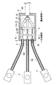
図1は、本発明多相超電導ケーブルの相分岐構造において、分岐端側にシールド接続部を具える例の概略構成図である。本例及び後述する実施例2では、図1及び図4に示すように3本のケーブルコア102を具える三相超電導ケーブル100の相分岐構造を例にして説明する。
【0027】
本発明相分岐構造は、超電導導体の外周にシールド層を有する3本のケーブルコア102と、3本のコア102が集合された集合部から各コア102間を広げた状態で各コア102を収納する分岐箱1と、分岐箱1内の各コア102のシールド層を接続するシールド接続部2とを具える。
【0028】
本例で用いた三相超電導ケーブル100は、図5に示すものと同様の構成のものである。即ち、中心から順にフォーマ200、超電導導体201、電気絶縁層202、シールド層203、保護層204を具えるケーブルコア102を3本撚り合わせて断熱管101内に収納された構成のものである。フォーマ200は、絶縁被覆された銅線を複数本撚り合わせたものを用いた。超電導導体201、シールド層203は、それぞれフォーマ200の外周、電気絶縁層202の外周にBi2223系超電導テープ線(Ag-Mnシース線)を多層に螺旋状に巻回して構成した。電気絶縁層202は、超電導導体201の外周に半合成絶縁紙(住友電気工業株式会社製PPLP:登録商標)を巻回して構成した。保護層204は、シールド層203の外周にクラフト紙を巻回して構成した。断熱管101は、SUSコルゲート管を用い、外管101aと内管101b間に断熱材を多層に配置して真空引きした真空多層断熱構造とした。また、断熱管101の外周には、ポリ塩化ビニルからなる防食層104を設けた。
【0029】
上記三相超電導ケーブル100の撚り合わされた各コア102は、それぞれ別個に取り扱い易くするべく、集合されていたケーブル100の各コア102間の間隔を広げられ分岐される。分岐箱1は、これら3本のケーブルコア102間の間隔が徐々に広げられた状態のコア102を収納する。従って、分岐箱1の一面側(図1では右面側)には、超電導ケーブル100が挿入され、この面と対向する他面側(同左面側)からは、分岐させた各コア102がそれぞれ突出される。また、分岐箱1内には、液体窒素などの冷媒が満たされ、収納されたケーブルコア102を冷却する。そのため、分岐箱1は、断熱層1aを具える断熱構造とした。また、本例において分岐箱1は、円筒状とした。
【0030】
分岐箱1内に収納されるケーブルコア102は、箱1の一面側(超電導ケーブル100の集合部側)から箱1の他面側(コア102の分岐端側)に向かって、各コア102間の間隔が徐々に広げられ、一定の間隔が保持されている。本例においてケーブルコア102の保持は、集合部側を保持する第一保持具10と、中間部を保持する第二保持具11と、第一保持具10と第二保持具11間のコア102を保持する中間保持具12とで行う。
【0031】
第一保持具10は、中心に環状部を具え、この環状部の外周に三つの中間保持具12が固定される。この第一保持具10は、3本のケーブルコア102で囲まれる空間のほぼ中心部に環状部の中心が位置するようにコア102間に配置し、各中間保持具12にそれぞれコア102を配置することで、コア102間の間隔を広げた状態に保持する。
【0032】
第二保持具11の基本的構成は、第一保持具10とほぼ同様の構成であり、環状部の径を第一保持具10よりも大きくしたものである。本例では、ケーブルコア102の伸縮に伴って分岐箱1内を移動できるように、箱1の内周面にほぼ点接触するような摺動部11aを具える。この摺動部11aは、環状部の外周で中間保持具12を固定していない個所に取り付けている。
【0033】
中間保持具12は、半円弧状の部材、いわゆる樋状の部材を組み合わせて円筒状とする構成である。本例では、一対の樋状の部材によりケーブルコア102の外周を覆い、この樋状の部材の外周をバンド(図示せず)などの締付具によりコア102の外周に固定し、コア102を保持する。また、中間保持具12内のケーブルコア102が冷媒と接触し易いように、保持具12に適宜貫通孔を設けてもよい。
【0034】
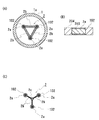
そして、本発明の特徴とするところは、各ケーブルコア102のシールド層同士をシールド接続部2にて接続する構成にある。即ち、本発明において各ケーブルコア102のシールド層は、シールド接続部2を介して閉ループを形成する。本例では、上記第二保持具11よりも分岐端側に位置するケーブルコア102のシールド層同士をシールド接続部2にて接続した。図2(A)は、図1のB-B断面図、(B)は、図1に示す領域C内のケーブルコア部分の断面図である。本例においてシールド接続部2は、図2に示すように各ケーブルコア102のシールド層203の外周をそれぞれ覆う円筒状部材2aと、円筒状部材2a同士を連結する連結部材2bとを具える。
【0035】
円筒状部材2aは、各ケーブルコア102のシールド層203の外周に取り付け易いように、コア102の外形に適合した一対の半円弧状部材から構成され、これら半円弧状部材を組み合わせることでシールド層203の外周を覆う。より具体的には、図2(B)に示すようにケーブルコア102の保護層204の一部を除去してシールド層203を露出させ、露出させたシールド層203上に一対の半円弧状部材を配置してコア102を覆う。本例において円筒状部材2aは、銅にて形成した。本例において半円弧状部材同士の接合は、半田にて行ったが、ボルトなどの結合部材を用いて行ってもよい。また、各円筒状部材2aと各ケーブルコア102のシールド層203の接合は、半田にて行い、シールド層203を構成する複数の超電導テープ線に円筒状部材2aを接触させた。
【0036】
連結部材2bは、円筒状部材2a同士を接続すると共に、ケーブルコア102間に配置されるものであり、上記円筒状部材2aと同様に銅にて形成した。本例では、3組の連結部材2bを用い、各連結部材2bの両端に円筒状部材2aを接合し、図2(A)に示すように円筒状部材2aを頂点とする三角形状にシールド接続部2を形成した(Δ結線型)。本例において連結部材2bと円筒状部材2aの接合は、半田にて行ったが、ボルトなどの結合部材を用いて行ってもよい。また、図2(C)に示すように、円筒状部材2aを頂点とする三角形の中心に中心部材2cを配置し、この中心部材2cと各円筒状部材2a間を連結するように連結部材2bを接合してシールド接続部2を形成してもよい(Y結線型)。
【0037】
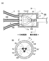
上記連結部材のより詳細な構成を説明する。図3は、シールド接続部において連結部材部分を拡大して示す概略図であり、(A)は、銅板に超電導線材を縦添えした連結部材の例、(B)は、一対の銅板片間を超電導線材にて連結させた連結部材の例である。図3(A)に示す例では、銅板20に超電導線21を縦添えして半田により接合した板状の連結部材である。本例では、超電導線21として、パウダーインチューブ法により形成したものを用いた。具体的には、Bi2223相からなる原料粉末をAgパイプに挿入した後、伸線してクラッド線材とし、このクラッド線材を複数本束ねてAgパイプに挿入した後、伸線して多心線材とし、この多心線材に圧延加工及び熱処理を施して得られたテープ線を用いた。
【0038】
図3(B)に示す例では、一対の銅板片22に超電導線23を並列に配置し、超電導線23の両端をそれぞれ銅板片22に半田にて接合した連結部材である。本例では、超電導線23として、上記と同様にパウダーインチューブ法により形成した多心線材に熱処理を施して得られた丸線を用いた。本例に示す連結部材2bの中間部は、超電導線23のみで構成される。従って、上記図3(A)に示す例と比較して、シールド接続部2の接続間抵抗をより小さくすることができる。また、丸線を用いたことで、連結部材2bの中間部が超電導線23のみであっても機械的強度に優れる。なお、丸線の代わりに上記と同様のテープ線を用いてもよい。このとき、より強度を高めるために、テープ線を複数枚積層して半田付けしたものを用いてもよい。
【0039】
また、本例では、図1に示すように分岐箱1から引き出された各ケーブルコア102の外周には、それぞれ絶縁材料であるFRPからなる断熱管3を配置しており、管3内には、箱1内と同様に冷媒が満たされる。従って、分岐箱1から突出した各ケーブルコア102も超電導状態を維持することができる。また、断熱管3の材料として、絶縁性のFRPを用いたことで、シールド接続部2から端末部4までのケーブルコア102の外周に漏洩磁場が発生しても、渦電流が生じにくい、或いは全く生じない。従って、渦電流による損失を低減することができる。なお、各ケーブルコア102の分岐端には、他のケーブルコアや接続機器などと接続可能な端末部4をそれぞれ設けている。これは、後述する実施例2についても同様である。
【0040】
上記構成を具える超電導ケーブルの相分岐構造は、超電導材料を用いたシールド接続部にて各ケーブルコアのシールド層同士を接続することで、ケーブルに電流を流すと、シールド層間は短絡された状態となる。即ち、シールド層間は、接続間抵抗が小さい状態で接続されるため、各シールド層に流れる電流の大きさを各超電導導体に流れる電流とそれぞれほぼ同等とすることができる。従って、各シールド層には、各超電導導体から発生する磁場を打ち消す程度の磁場を形成することができるため、ケーブルコアの外部に大きな磁場が発生することを効果的に抑制することができる。また、シールド接続部に超電導材料を用いることで、シールド層の接続間抵抗を非常に小さくすることができるため、同接続部に通電されることで生じる発熱量は小さく、冷凍機の負荷を過度に大きくすることがない。
【0041】
更に、本例では、分岐端側にシールド接続部を取り付けているため、各ケーブルコア間が十分に広げられた状態の個所に取り付け作業を行うことができ、同接続部の取り付け作業性に優れる。
【0042】
(実施例2)
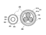
図4(A)は、本発明多相超電導ケーブルの相分岐構造において、集合部側にシールド接続部を具える例を示す概略構成図であり、(B)は、(A)のB-B断面図である。図4(A)において端末部は、省略している。この本発明相分岐構造は、基本的構成は図1に示す実施例1と同様であり、シールド接続部2'を第二保持具11よりも集合部側に取り付けた点が異なる。以下、この点を中心に説明する。
【0043】
本例に示すシールド接続部2'は、図4(B)に示すように、各ケーブルコア102のシールド層の外周をそれぞれ覆う円筒状部材2a'と、円筒状部材2a'同士を連結する連結部材2b'とを具える。本例において円筒状部材2a'は、実施例1と同様に一対の半円弧状部材からなる銅製のものを用い、ケーブルコア102の保護層204の一部を除去して露出させたシールド層の外周に配置し、ボルトにより接合することでコア102を覆った。また、各円筒状部材2a'と各ケーブルコア102のシールド層203の接合は、半田にて行った。
【0044】
本例において連結部材2b'は、円筒状部材2a同士を接続すると共に、ケーブルコア102間に配置されるものであり、三角形状の板材の頂点部分を円弧状に切り欠いた形状で、円筒状部材2a'と同様の銅にて形成した。そして、本例では、連結部材2b'の各切り欠き部分に円筒状部材2a'を配置して接合し、図4(B)に示すように円筒状部材2a'を頂点とする三角形状にシールド接続部2'を形成する(Δ結線型)。本例において連結部材2b'と円筒状部材2a'の接合は、半田にて行ったが、ボルトなどの結合部材を用いて行ってもよい。
【0045】
上記連結部材のより詳細な構成を説明する。図4(B)に示すように、本例では、銅板24に超電導線25を配置して、半田により接合している。超電導線25は、円筒状部材2a'を連結するように、即ち、図4(B)に示すように三角形状となるように配置している。本例において超電導線25は、上記実施例1と同様にパウダーインチューブ法により形成したテープ線を用いた。
【0046】
上記構成を具える超電導ケーブルの相分岐構造は、超電導材料を用いたシールド接続部にて各ケーブルコアのシールド層を接続することで、ケーブルに電流を流した際、上記実施例1と同様にシールド層の接続間抵抗を小さくすることができる。従って、各シールド層に流れる電流の大きさを超電導導体に流れる電流とほぼ同等にして、各導体から発生する磁場を各シールド層から発生する磁場にて打ち消すことができる。そのため、本発明相分岐構造は、ケーブルコアの外部に大きな磁場が発生することを効果的に抑制することができる。また、シールド接続部に超電導材料を利用することによりシールド層の接続間抵抗が極めて小さいことで、同接続部の通電により発生する熱が少なく、冷凍機の負荷を過度に大きくすることがない。
【0047】
更に、本例では、集合部側にシールド接続部を配置しているため、各ケーブルコア間の距離が小さいため、シールド接続部を小さくすることができ、分岐箱において第二保持具よりも分岐端側の空間を小さくすることができる。従って、分岐箱をよりコンパクトにすることができる。
【0048】
(実施例3)
上記実施例1及び2では、パウダーインチューブ法により形成される超電導線、即ち、超電導相と金属とからなる超電導体を用いたシールド接続部を説明した。この例では、基本的構成を上記実施例1と同様とし、超電導相のみからなる超電導体を用いたシールド接続部を用いる例を説明する。具体的には、図1に示す例において、超電導線23(図3(B)参照)としてBi2223の酸化物超電導相からなるバルク超電導体を用いる。本例では、棒状に形成したバルク超電導体を用いた。
【0049】
本例に示すシールド接続部は、連結部材に銀などの金属を介在させていないバルク超電導体を用いる。そして、このバルク超電導体は、銅板などに縦添えせずに用いる。この構成により、Bi2223系超電導テープ線(Ag-Mnシース線)から形成されるシールド層よりも臨界電流値を小さくし、かつ常電導抵抗を大きくすることができる。従って、短絡事故などの事故が発生して超電導導体に短絡電流が流れた際、シールド接続部が導体よりも先に臨界電流値を超えて大抵抗となることで、導体からシールド層に誘起される電流を小さくすることができる。従って、事故時の電流によるシールド層の損傷を低減、或いは抑制することができる。また、上記事故時、シールド接続部が短絡電流により損傷することがあっても、損傷部分を確認し易く、損傷部分の交換が同接続部のみで済むため、事故処理を容易に行うことができる。
【0050】
(実施例4)
次に、基本的構成を上記実施例2と同様とし、Re系酸化物超電導体を用いたシールド接続部を用いる例を説明する。具体的には、図4に示す例において、銅板24の代わりに基板としてNi合金板、具体的にはハステロイ(ヘインズ社登録商標)を用い、この合金板の上に公知のPVDによりYBa2Cu3Ox膜を成膜した超電導体を用いる。
【0051】
本例に示すシールド接続部は、希土類超電導体を用いることから、短絡事故などの事故が発生して超電導導体に短絡電流が流れても、上記実施例3と同様に同接続部の抵抗を大きくすることができるため、シールド層に誘起される電流を小さくすることができる。従って、事故時の電流によるシールド層の損傷を低減、或いは抑制することができる。また、上記事故時、シールド接続部が短絡電流により損傷することがあっても、損傷部分を確認し易く、損傷部分の交換が同接続部のみで済むため、事故処理を容易に行うことができる。更に、超電導層を成膜により形成するため、基板の形状を任意に変更することができ、任意の形状の連結部材を形成することができる。
【0052】
【発明の効果】
以上、説明したように本発明超電導ケーブルの相分岐構造によれば、各ケーブルコアのシールド層同士の接続に導電性材料を用いるため、シールド層の接続間抵抗を非常に小さくすることができ、超電導導体に電流を流すと、各コアのシールド層には、導体に流れる電流と大きさがほぼ同じで反対方向の電流が流れて、導体に流れる電流により発生する磁場を効果的に相殺することができる。従って、本発明は、ケーブルコアの外部に大きな磁場が発生することを効果的に抑制することができる。
【0053】
また、シールド接続部の臨界電流値をケーブルコアのシールド層の臨界電流値よりも小さくすることで、短絡事故などの事故の際、同接続部は、臨界電流値を越えた後、大きな抵抗を生じることで、シールド層に誘起される電流を抑制することができる。従って、本発明は、事故時に誘起される大電流によるシールド層の損傷を小さく、或いは皆無にすることが可能である。また、シールド接続部が事故時の大電流により損傷することがあっても、損傷個所の特定が容易であり、接続部の交換も容易に行うことができる。
【図面の簡単な説明】
【図1】本発明多相超電導ケーブルの相分岐構造において、分岐端側にシールド接続部を具える例を示す概略構成図である。
【図2】 (A)は、図1のB-B断面図、(B)は、図1に示す領域C内のケーブルコア部分の断面図、(C)は、導電性接続部の別の形態を示す断面図である。
【図3】本発明多相超電導ケーブルの相分岐構造のシールド接続部において連結部材部分を拡大して示す概略図であり、(A)は、銅板に超電導線を縦添えした連結部材の例、(B)は、一対の銅板片間を超電導線材にて接続させた連結部材の例である。
【図4】 (A)は、本発明多相超電導ケーブルの相分岐構造において、集合部側にシールド接続部を具える例を示す概略構成図であり、(B)は、(A)のB-B断面図である。
【図5】三心一括型の三相超電導ケーブルの断面図である。
【符号の説明】
1 分岐箱 1a 断熱層 2 シールド接続部 2a、2a' 円筒状部材
2b 連結部材 2b' 連結部材 3 断熱管 4 端末部
10 第一保持具 11 第二保持具 11a 摺動部 12 中間保持具
20、24 銅板 21、23、25 超電導線 22 銅板片
100 三相超電導ケーブル 101 断熱管 101a 外管 101b 内管
102 ケーブルコア 103 空間 104 防食層
200 フォーマ 201 超電導導体 202 電気絶縁層 203 シールド層
204 保護層[0001]
BACKGROUND OF THE INVENTION
The present invention relates to a branching structure in which a multiphase superconducting cable composed of a plurality of cable cores is branched for each core. In particular, the present invention relates to a phase branching structure of a multiphase superconducting cable that hardly generates a magnetic field outside each cable core at a branching portion.
[0002]
[Prior art]
Conventionally, in a superconducting cable using a superconducting conductor made of a Bi-based high-temperature superconducting tape wire or the like, a multicore multi-phase superconducting cable in which a plurality of cable cores are collectively developed is being developed. FIG. 5 is a cross-sectional view of a three-core superconducting cable of a three-core package type. The
[0003]
The
[0004]
The multi-phase superconducting cable is branched into each phase, that is, for each cable core, when these cables are connected to each other, connected to a normal conducting cable, or a termination structure is formed. The branching of each cable core is performed in a branching box maintained at an extremely low temperature, and each core is held in the branching box in a state where the space between the cores is widened. There is one described in
[0005]
On the other hand, the normal conducting multiphase power cable is also branched for each cable core in the case of connecting the cables or forming a termination structure, like the multiphase superconducting cable. The branching of each cable core is performed by using a state where the cores are spread as they are without using the branch box as described above. In this branch portion, the shield layer of each cable core is normally grounded in order to take the ground potential of each phase (see, for example, Non-Patent Document 1).
[0006]
[Patent Document 1]
Japanese Patent Laid-Open No. 2003-9330 (refer to claims)
[Non-Patent Document 1]
Kihachiro Iizuka, “New Edition, Power Cable Technology Handbook”, Denki Shoin Co., Ltd., March 25, 1989, 1st edition, 1st edition, 645 pages
[0007]
[Problems to be solved by the invention]
Conventionally, there is no known processing method for the shield layer of each cable core at the branch portion of the multiphase superconducting cable, and specific processing is desired. Here, similarly to the normal conducting cable, it is conceivable to ground the shield layer of each cable core also in the superconducting cable. However, since the superconducting cable passes a much larger current than the normal conducting cable, if the shield layer is grounded like the normal conducting cable, the shield layer of each cable core may be connected through the earth (ground). And when the shield layer of each cable core is connected via the ground, there is a problem that the magnetic field generated outside each core increases. If the shield layer of each cable core of a superconducting cable is grounded and the shield layers are connected via ground, the resistance between the shield layers is large, so the magnitude of the current flowing in the shield layer is the current flowing in the superconductor. Smaller than. For this reason, the shield layer of each cable core cannot form a magnetic field enough to cancel the magnetic field generated from the superconducting conductor of each core, and a large magnetic field may be generated outside each core.
[0008]
Therefore, a main object of the present invention is to provide a phase branching structure of a multiphase superconducting cable in which a magnetic field is hardly generated outside each cable core.
[0009]
Another object of the present invention is to provide a phase branching structure of a multiphase superconducting cable capable of suppressing a current induced in a shield layer by a short circuit current flowing in a superconducting conductor when an accident such as a short circuit accident occurs. There is to do.
[0010]
[Means for Solving the Problems]
The present invention achieves the above object by connecting the shield layers of the cable cores at the shield connection portion using the superconducting material and connecting the shield layers with lower resistance.
[0011]
That is, the phase branching structure of the multiphase superconducting cable of the present invention has a plurality of cable cores having a shield layer on the outer periphery of the superconducting conductor, and a state where each cable core is widened from an assembly portion where the plurality of cable cores are assembled. A branch box for storing each core and a shield connection part for connecting shield layers of the cable cores in the branch box are provided, and a superconducting material is used for the shield connection part.
[0012]
In a multiphase superconducting cable, when the shield layer of each cable core is connected via the ground, the resistance between the shield layers is large. Therefore, the shield layer of each core cancels the magnetic field generated from the superconducting conductor of each core. Hard to generate a magnetic field. Therefore, the present invention stipulates that the shield layer is connected by using a conductive material having a low connection resistance, particularly a superconducting material, instead of connecting the shield layers of each cable core by grounding that increases the connection resistance. To do.
[0013]
With the above configuration, the present invention can reduce the resistance between the shield layers when current is passed through the superconducting cable so that the current flowing through the shield layer of each cable core is substantially equal to the current flowing through the superconducting conductor. it can. Therefore, the present invention can substantially cancel the magnetic field generated from the superconducting conductor of each cable core by the magnetic field generated in the shield layer of each core, thereby further reducing or eliminating the leakage magnetic field generated outside each core. It is possible. In the present invention, in particular, the superconducting material is used for the shield connection portion, and the resistance between the shield layers is small. It is also possible to do. Hereinafter, the present invention will be described in more detail.
[0014]
The present invention is directed to a multiphase superconducting cable having a plurality of cable cores having shield layers on the outer periphery of the superconducting conductor. For example, a three-core one-phase superconducting cable in which three cable cores are twisted and stored in a heat insulating tube can be mentioned. A known multiphase superconducting cable may be used.
[0015]
Moreover, in this invention, a branch box is used in order to accommodate the core which branched the multiphase superconducting cable for every cable core. That is, the branch box accommodates cores in a state where each core is expanded from an aggregate portion where a plurality of cable cores constituting the multiphase superconducting cable are aggregated. The branch box is filled with a refrigerant such as liquid nitrogen for cooling the cable cores to maintain the superconducting state. Therefore, it is desirable that the branch box has a heat insulating structure.
[0016]
Each cable core may be held in the branch box using a holder. Examples of the holding tool can hold each cable core and can hold the cable core in a state where the cores are widened. In particular, a holder having a configuration that can move in the branch box as the cable core expands and contracts is preferable.
[0017]
And in this invention, in each cable core accommodated in the said branch box, shield layers are connected by the specific connection part, specifically, the shield connection part using a superconducting material. The shield connection part should just connect at least one part shield layer with respect to the longitudinal direction of the shield layer of each cable core accommodated in a branch box. Moreover, the shape of the shield connection part should just be a shape which touches at least one part with respect to the circumferential direction of the shield layer of each cable core, and can connect the shield layer of each core. When the shield layer of each cable core is formed of a plurality of superconducting strands, it is preferable that the shield layer has a shape that can be electrically connected to all the superconducting strands to be configured. For example, the shape which combined the cylindrical member which covers the outer periphery of the shield layer of each cable core, and the connection member which connects this cylindrical member is mentioned. In the present invention, a superconducting material is used for at least a part of such a shield connection portion. For example, the cylindrical member may be formed of a metal such as copper or aluminum having excellent attachment workability, and a superconducting material may be used for the connecting member. For example, the structure which connects metal cylindrical members with a superconducting wire is mentioned. In the connecting member, a metal such as copper or aluminum and a superconducting material may be used in combination. For example, a superconducting wire is vertically attached to a metal plate, or a pair of metal plate pieces are connected by a superconducting wire.
[0018]
Examples of the superconducting material include a superconducting tape wire using a Bi-based oxide superconductor such as the Bi2223 phase similar to that used for a superconducting conductor and a shield layer, and a round wire used for manufacturing this tape wire. Examples include superconducting wires. Examples of these superconducting tape wires and round wires include those formed by a powder-in-tube method. Specifically, after inserting the superconducting phase raw material powder such as Bi2223 phase into a metal pipe such as Ag, it is drawn into a clad wire, and after bundled a plurality of this clad wire is inserted into a metal pipe such as Ag The wire is drawn into a multi-core wire. A round wire is obtained by heat-treating this multi-core wire to obtain the desired superconducting phase. On the other hand, a tape wire is obtained by subjecting this multi-core wire to rolling and heat treatment. When round wire is used, (1) fewer manufacturing steps are required compared to tape wire, (2) because the cross section is circular, the structure is stronger than tape wire, and (3) from tape wire. Are easy to handle and have excellent workability.
[0019]
Here, if an accident such as a short-circuit accident occurs and a short-circuit current flows through the superconducting conductor and a large current is induced in the shield layer, the temperature of the shield layer rises due to this large current and the superconducting state can be maintained. There is a risk that so-called quenching occurs, which shifts to the normal conducting state. Therefore, it is desired to effectively suppress a large current induced in the shield layer at the time of an accident. As a countermeasure, for example, the critical current value of the shield connecting portion can be made smaller than the critical current value of the shield layer of the cable core. With this configuration, when a short circuit accident or the like occurs and a large current is induced in the shield layer and the shield connection part, the connection part exceeds the critical current value before the shield layer, and then generates a large resistance. Thus, the current induced in the shield layer can be suppressed. In other words, by quenching the shield connection portion before the shield layer, the damage caused to the shield layer by the current induced at the time of the accident can be reduced or eliminated. Further, even if the shield connection portion is damaged by a large current at the time of the accident, not only the damaged portion can be easily identified, but only the connection portion needs to be replaced, and the accident processing can be easily performed.
[0020]
In order to make the critical current value of the shield connection part smaller than the critical current value of the shield layer, that is, to make the connection part have a higher resistance in the event of an accident, it is necessary to devise a superconducting material used for the connection part. It is done. For example, when using a superconducting material formed by the powder-in-tube method, the number of superconducting wires used can be reduced. In addition, it is possible to use a superconducting wire in which the number of clad wires of the multi-core wire is smaller than that of the superconducting wire used for the shield layer. In addition, for example, a superconducting material other than the superconducting material formed by the powder-in-tube method, specifically, a superconductor composed of only a superconducting phase without a metal matrix such as Ag as described above, a so-called bulk superconductor can be mentioned. . Specific examples of the superconducting phase include the Bi-based oxide superconducting phase and rare earth oxide superconducting materials such as the composition formula Re-Ba-Cu-O (representing lanthanum-based elements such as Re: Y, Sm, Nd, Pr). Phase. The specific composition of the rare earth oxide superconducting phase is YBa 2 Cu Three Ox, Y 2 BaCuOx, NdBa 2 Cu Three Ox, Nd Four Ba 2 Cu 2 Ox, SmBa 2 Cu Three Ox, Sm 2 BaCuOx, PrBa 2 Cu Three Ox, Pr 2 BaCuOx, HoBa 2 Cu Three Examples include Ox. Since such a bulk superconductor is composed only of an oxide phase without interposing a metal such as Ag, it easily becomes a large resistance in the event of an accident. These bulk superconductors are easy to use if they are formed in an appropriate shape, for example, a rod-like body or a plate-like body.
[0021]
In addition, as a superconducting material having a high resistance in the event of an accident, a superconductor in which the above-described Re-based superconducting layer is formed on a metal substrate can be cited. Examples of the metal substrate include those formed from a Ni alloy having a high melting point. The Re-based superconducting layer may be formed by using a known CVD method or PVD method. An intermediate layer such as yttria stabilized zirconia (YSZ) may be formed between the metal substrate and the Re-based superconducting layer. This superconductor is also easy to use if the metal substrate is formed in an appropriate shape, for example, a tape shape.
[0022]
The connection between the shield connection portion and the shield layer is preferably a method having a small electrical resistance due to the connection, such as a connection by solder. In addition, when attaching a shield connection part to a shield layer, when each cable core is provided with a protective layer, the protective layer at the connection point is removed in advance.
[0023]
The shield connection part may be attached to the shield layer of the cable core drawn out from the branch box, but each core protruding from the box has liquid nitrogen in order to maintain a superconducting state like the core in the box. Insulating tubes filled with a refrigerant such as are arranged. Therefore, since the structure which attaches a shield connection part to the shield layer of each cable core protruded from the branch box becomes very complicated, in this invention, a shield connection part is attached to the core in a branch box.
[0024]
In addition, the shield connecting portion may be attached to any position of each cable core disposed in the branch box. However, when attached to the branch end side, the distance between the cores is large because each core is further widened. Therefore, the attachment workability of the connection portion is good and preferable. On the other hand, when attaching to the assembly side, the distance between the cable cores is not widened and the distance is small, so that the shield connection part can be made small. In addition, since the shield connection portion is not on the branch end side, the branch end side of the branch box can be made smaller. That is, the branch box can be made smaller.
[0025]
The branch structure of the present invention is preferably formed not only at one end of the cable core (superconducting cable) but also at both ends. When the branch structure of the present invention is provided at both ends of the superconducting cable, a branch box is provided at both ends of the cable, and the shield layers of the cores housed in each branch box are connected to each other at the shield connection portion. At this time, the shield layer of each cable core between the shield connection part at one end of the superconducting cable and the shield connection part at the other end has a magnitude almost the same as the current flowing in each superconducting conductor in the normal direction and in the opposite direction. Current is induced, so that the leakage magnetic field to the outside of the core can be canceled. Since most of the current flowing in the superconducting conductor is almost equal to the current flowing in the opposite direction, it flows in the shield layer on the collecting end side of the shield connection portion, so the shield layer between the shield connection portion and the branch end Only a current smaller than the current flowing in the superconducting conductor flows. Therefore, if the heat insulation pipe disposed on the outer periphery of each cable core protruding from the branch box is formed of an electrically low resistance material, an eddy current is generated by a leakage magnetic field generated from the shield connection portion to the outer periphery of the cable core on the branch end side. There is a risk of loss. Therefore, in order to reduce or eliminate the loss due to eddy current, it is preferable to use the heat insulating tube made of a high resistance material or an insulating material. As a high resistance material, a specific resistance ρ at a low temperature of about 77K from room temperature is 10 -Five Those of Ω · cm or more are preferable. For example, stainless steel (specific resistance ρ: 4 × 10 -Five ~ 8 × 10 -Five Ωcm). Examples of the insulating material include FRP (fiber reinforced plastic).
[0026]
DETAILED DESCRIPTION OF THE INVENTION
Embodiments of the present invention will be described below.
(Example 1)
FIG. 1 is a schematic configuration diagram of an example in which a shield connection portion is provided on a branch end side in a phase branching structure of a multiphase superconducting cable of the present invention. In this example and Example 2 described later, a phase branching structure of a three-
[0027]
The phase branching structure of the present invention accommodates the three
[0028]
The three-
[0029]
The
[0030]
The
[0031]
The
[0032]
The basic structure of the
[0033]
The
[0034]
The feature of the present invention lies in the configuration in which the shield layers of the
[0035]
The
[0036]
The connecting
[0037]
A more detailed configuration of the connecting member will be described. FIG. 3 is an enlarged schematic view showing a connecting member portion in a shield connecting portion, (A) is an example of a connecting member in which a superconducting wire is vertically attached to a copper plate, and (B) is a space between a pair of copper plate pieces. It is an example of the connection member connected with the superconducting wire. The example shown in FIG. 3 (A) is a plate-like connecting member in which a
[0038]
In the example shown in FIG. 3 (B), a
[0039]
Further, in this example, as shown in FIG. 1,
[0040]
The phase branching structure of the superconducting cable having the above configuration is a state where the shield layers are short-circuited when a current is passed through the cable by connecting the shield layers of the cable cores at the shield connection portion using the superconducting material. It becomes. That is, since the shield layers are connected in a state where the resistance between the connections is small, the current flowing through each shield layer can be made substantially equal to the current flowing through each superconducting conductor. Therefore, each shield layer can be formed with a magnetic field that cancels out the magnetic field generated from each superconducting conductor, so that the generation of a large magnetic field outside the cable core can be effectively suppressed. In addition, the use of superconducting material for the shield connection can make the resistance between the shield layers very small, so the amount of heat generated by energizing the connection is small and the load on the refrigerator is excessive. Don't make it bigger.
[0041]
Furthermore, in this example, since the shield connection portion is attached to the branch end side, the attachment work can be performed at a location where the space between the cable cores is sufficiently widened, and the attachment workability of the connection portion is excellent. .
[0042]
(Example 2)
FIG. 4 (A) is a schematic configuration diagram showing an example in which a shield connection portion is provided on the assembly side in the phase branching structure of the multiphase superconducting cable of the present invention, and (B) is a BB cross-sectional view of (A). It is. In FIG. 4A, the terminal portion is omitted. The basic structure of the phase branching structure of the present invention is the same as that of the first embodiment shown in FIG. 1, except that the
[0043]
As shown in FIG. 4 (B), the
[0044]
In this example, the connecting
[0045]
A more detailed configuration of the connecting member will be described. As shown in FIG. 4B, in this example, the
[0046]
The phase branching structure of the superconducting cable having the above configuration is similar to the first embodiment when a current is passed through the cable by connecting the shield layer of each cable core at the shield connecting portion using the superconducting material. The resistance between the shield layers can be reduced. Therefore, the magnitude of the current flowing in each shield layer can be made substantially equal to the current flowing in the superconducting conductor, and the magnetic field generated from each conductor can be canceled by the magnetic field generated from each shield layer. Therefore, the phase branch structure of the present invention can effectively suppress the generation of a large magnetic field outside the cable core. Moreover, since the resistance between the shield layers is extremely small by using a superconducting material for the shield connection portion, there is little heat generated by energization of the connection portion, and the load on the refrigerator is not excessively increased.
[0047]
Furthermore, in this example, since the shield connection part is arranged on the collecting part side, the distance between the cable cores is small, so the shield connection part can be made smaller, and the branch box is branched than the second holder. The space on the end side can be reduced. Therefore, the branch box can be made more compact.
[0048]
(Example 3)
In Examples 1 and 2 described above, a shield connection portion using a superconducting wire formed by a powder-in-tube method, that is, a superconductor composed of a superconducting phase and a metal has been described. In this example, an example will be described in which the basic configuration is the same as that of the first embodiment, and a shield connection portion using a superconductor composed of only a superconducting phase is used. Specifically, in the example shown in FIG. 1, a bulk superconductor composed of an oxide superconducting phase of Bi2223 is used as the superconducting wire 23 (see FIG. 3B). In this example, a bulk superconductor formed in a rod shape was used.
[0049]
The shield connecting portion shown in this example uses a bulk superconductor in which a metal such as silver is not interposed in the connecting member. The bulk superconductor is used without being vertically attached to a copper plate or the like. With this configuration, the critical current value can be made smaller than that of the shield layer formed from the Bi2223 superconducting tape wire (Ag-Mn sheath wire), and the normal conduction resistance can be made larger. Therefore, when an accident such as a short-circuit accident occurs and a short-circuit current flows through the superconducting conductor, the shield connection part exceeds the critical current value before the conductor and becomes a large resistance, which is induced from the conductor to the shield layer. Current can be reduced. Therefore, damage to the shield layer due to current at the time of an accident can be reduced or suppressed. Moreover, even if the shield connection part may be damaged by a short-circuit current at the time of the accident, the damaged part can be easily confirmed, and the damaged part can be replaced only by the connection part, so that the accident process can be easily performed. .
[0050]
(Example 4)
Next, an example will be described in which the basic configuration is the same as that of the second embodiment and a shield connection portion using a Re-based oxide superconductor is used. Specifically, in the example shown in FIG. 4, instead of the copper plate 24, a Ni alloy plate, specifically Hastelloy (registered trademark of Haynes), is used as a substrate. 2 Cu Three A superconductor with an Ox film is used.
[0051]
Since the shield connection part shown in this example uses a rare earth superconductor, even if an accident such as a short-circuit accident occurs and a short-circuit current flows through the superconducting conductor, the resistance of the connection part is increased as in Example 3 above. Therefore, the current induced in the shield layer can be reduced. Therefore, damage to the shield layer due to current at the time of an accident can be reduced or suppressed. Moreover, even if the shield connection part may be damaged by a short-circuit current at the time of the accident, the damaged part can be easily confirmed, and the damaged part can be replaced only by the connection part, so that the accident process can be easily performed. . Furthermore, since the superconducting layer is formed by film formation, the shape of the substrate can be arbitrarily changed, and a connecting member having an arbitrary shape can be formed.
[0052]
【The invention's effect】
As described above, according to the phase branching structure of the superconducting cable of the present invention, since the conductive material is used for the connection between the shield layers of each cable core, the resistance between the connection of the shield layers can be greatly reduced. When a current is passed through a superconducting conductor, the current flowing in the opposite direction flows through the shield layer of each core in the same direction, effectively canceling out the magnetic field generated by the current flowing in the conductor. Can do. Therefore, the present invention can effectively suppress the generation of a large magnetic field outside the cable core.
[0053]
In addition, by making the critical current value of the shield connection part smaller than the critical current value of the shield layer of the cable core, in the event of an accident such as a short circuit accident, the connection part has a large resistance after exceeding the critical current value. As a result, the current induced in the shield layer can be suppressed. Therefore, the present invention can reduce or eliminate damage to the shield layer due to a large current induced at the time of an accident. Further, even if the shield connection portion is damaged by a large current at the time of an accident, it is easy to identify the damaged portion, and the connection portion can be easily replaced.
[Brief description of the drawings]
FIG. 1 is a schematic configuration diagram showing an example in which a shield connecting portion is provided on a branch end side in a phase branching structure of a multiphase superconducting cable of the present invention.
2A is a cross-sectional view taken along the line BB in FIG. 1, FIG. 2B is a cross-sectional view taken along the cable core in the region C shown in FIG. 1, and FIG. It is sectional drawing shown.
FIG. 3 is an enlarged schematic view showing a connecting member portion in a shield connecting portion of a phase branching structure of a multiphase superconducting cable of the present invention, (A) is an example of a connecting member in which a superconducting wire is vertically attached to a copper plate; (B) is an example of a connecting member in which a pair of copper plate pieces are connected by a superconducting wire.
FIG. 4A is a schematic configuration diagram showing an example in which a shield connection portion is provided on the assembly side in the phase branching structure of the multiphase superconducting cable of the present invention, and FIG. It is sectional drawing.
FIG. 5 is a cross-sectional view of a three-core collective three-phase superconducting cable.
[Explanation of symbols]
1
10
20, 24
100 Three-
102
200 Former 201
204 Protective layer
Claims (6)
前記複数のケーブルコアが集合された集合部から各ケーブルコア間を広げた状態で各コアを収納する分岐箱と、
分岐箱内の各ケーブルコアのシールド層同士を接続するシールド接続部とを具え、
前記シールド接続部に超電導材料を用いており、
前記シールド接続部の臨界電流値がシールド層の臨界電流値よりも小さいことを特徴とする多相超電導ケーブルの相分岐構造。A plurality of cable cores having a shield layer on the outer periphery of the superconducting conductor;
A branch box for storing each core in a state where each cable core is widened from a gathering portion where the plurality of cable cores are gathered;
A shield connection for connecting the shield layers of each cable core in the branch box,
Superconducting material is used for the shield connection part ,
A phase branching structure of a multiphase superconducting cable, wherein a critical current value of the shield connection portion is smaller than a critical current value of a shield layer .
前記連結部材の少なくとも一部が超電導材料により構成されていることを特徴とする請求項1に記載の多相超電導ケーブルの相分岐構造。 The shield connecting portion is composed of a cylindrical member that covers the outer periphery of the shield layer of each cable core, and a connecting member that connects the cylindrical members,
The phase branching structure of a multiphase superconducting cable according to claim 1, wherein at least a part of the connecting member is made of a superconducting material .
前記超電導線材は、パウダーインチューブ法により形成されたテープ線であることを特徴とする請求項 The superconducting wire is a tape wire formed by a powder-in-tube method. 22 に記載の多相超電導ケーブルの相分岐構造。The phase branching structure of the multiphase superconducting cable described in 1.
Priority Applications (9)
| Application Number | Priority Date | Filing Date | Title |
|---|---|---|---|
| JP2003174666A JP4201331B2 (en) | 2003-06-19 | 2003-06-19 | Phase branching structure of multiphase superconducting cable |
| CA2468216A CA2468216C (en) | 2003-06-19 | 2004-05-26 | Phase split structure of multiphase superconducting cable |
| DK04013452.0T DK1492200T3 (en) | 2003-06-19 | 2004-06-08 | Phase divided structure of a multi-phase superconducting cable |
| EP04013452A EP1492200B1 (en) | 2003-06-19 | 2004-06-08 | Phase split structure of multiphase superconducting cable |
| US10/862,340 US7148423B2 (en) | 2003-06-19 | 2004-06-08 | Phase split structure of multiphase superconducting cable |
| TW093117267A TW200514101A (en) | 2003-06-19 | 2004-06-16 | Phase split structure of multiphase superconducting cable |
| KR1020040044906A KR100847681B1 (en) | 2003-06-19 | 2004-06-17 | Phase split structure of multiphase superconducting cable |
| CNB2004100597235A CN1316513C (en) | 2003-06-19 | 2004-06-21 | Phase split structure of multiphase superconducting cable |
| HK05102048A HK1069670A1 (en) | 2003-06-19 | 2005-03-09 | Phase split structure of multiphase superconducting cable |
Applications Claiming Priority (1)
| Application Number | Priority Date | Filing Date | Title |
|---|---|---|---|
| JP2003174666A JP4201331B2 (en) | 2003-06-19 | 2003-06-19 | Phase branching structure of multiphase superconducting cable |
Publications (2)
| Publication Number | Publication Date |
|---|---|
| JP2005012927A JP2005012927A (en) | 2005-01-13 |
| JP4201331B2 true JP4201331B2 (en) | 2008-12-24 |
Family
ID=33410979
Family Applications (1)
| Application Number | Title | Priority Date | Filing Date |
|---|---|---|---|
| JP2003174666A Expired - Fee Related JP4201331B2 (en) | 2003-06-19 | 2003-06-19 | Phase branching structure of multiphase superconducting cable |
Country Status (9)
| Country | Link |
|---|---|
| US (1) | US7148423B2 (en) |
| EP (1) | EP1492200B1 (en) |
| JP (1) | JP4201331B2 (en) |
| KR (1) | KR100847681B1 (en) |
| CN (1) | CN1316513C (en) |
| CA (1) | CA2468216C (en) |
| DK (1) | DK1492200T3 (en) |
| HK (1) | HK1069670A1 (en) |
| TW (1) | TW200514101A (en) |
Families Citing this family (20)
| Publication number | Priority date | Publication date | Assignee | Title |
|---|---|---|---|---|
| FR2878654B1 (en) * | 2004-12-01 | 2007-01-12 | Nexans Sa | CONNECTING ARRANGEMENT FOR SUPERCONDUCTING CABLES SCREENS |
| KR100706491B1 (en) * | 2005-03-03 | 2007-04-10 | 엘에스전선 주식회사 | Cryostat for three superconducting cable |
| KR100706494B1 (en) * | 2006-01-20 | 2007-04-10 | 엘에스전선 주식회사 | Superconducting cable |
| CN101982902B (en) * | 2010-09-14 | 2013-03-20 | 上海电缆研究所 | Interconnecting structure for low-temperature insulation superconducting cable shielding conductor |
| US8850832B2 (en) * | 2011-01-25 | 2014-10-07 | Friedrich Air Conditioning Co, Ltd. | Apparatus and method for installation by unlicensed personnel of a pre-charged, ductless heating/cooling system |
| KR101800017B1 (en) | 2011-02-15 | 2017-11-21 | 엘에스전선 주식회사 | Conductor Insulation Method for High Voltage Cable |
| KR101798659B1 (en) * | 2011-04-27 | 2017-11-16 | 엘에스전선 주식회사 | Super-conducting cable device |
| JP5724703B2 (en) * | 2011-07-14 | 2015-05-27 | 住友電気工業株式会社 | Method and apparatus for starting superconducting cable |
| CN103311764A (en) * | 2012-03-06 | 2013-09-18 | 刘彩声 | Switching device |
| US8608496B2 (en) | 2012-04-25 | 2013-12-17 | Pratt & Whitney Canada Corp. | Connector for multi-phase conductors |
| EP2690737B1 (en) * | 2012-07-25 | 2017-08-30 | Nexans | Assembly with three superconducting phase conductors |
| EP2819247B1 (en) * | 2013-06-25 | 2018-08-08 | Nexans | Method for connecting two superconductive cables in a manner that conducts electricity |
| CN104409168A (en) * | 2014-12-12 | 2015-03-11 | 吕珩 | Triangular shielding layer of three-phase superconducting cable |
| JP6471625B2 (en) * | 2015-06-25 | 2019-02-20 | 新日鐵住金株式会社 | Superconducting conductive element |
| CN106531326B (en) * | 2016-12-12 | 2018-06-01 | 深圳市金洋电子股份有限公司 | A kind of waterproof method for photovoltaic cable water proof type SR structures |
| CN110474284B (en) * | 2019-09-07 | 2020-07-24 | 埃塞克斯电气(南京)有限公司 | Three-core cable terminal shaping device |
| CN111029035A (en) * | 2019-12-26 | 2020-04-17 | 国网江苏省电力有限公司 | High-temperature superconducting cable structure and high-temperature superconducting cable system |
| KR20220080429A (en) * | 2020-12-07 | 2022-06-14 | 에스케이하이닉스 주식회사 | Image sensing device |
| CN114284761B (en) * | 2021-12-21 | 2023-09-12 | 深圳供电局有限公司 | Superconducting cable adapter |
| CN115911897B (en) * | 2023-03-13 | 2023-05-16 | 中国科学院合肥物质科学研究院 | Sleeve joint terminal, sleeve joint and preparation method of sleeve joint |
Family Cites Families (6)
| Publication number | Priority date | Publication date | Assignee | Title |
|---|---|---|---|---|
| JP3467295B2 (en) * | 1993-09-13 | 2003-11-17 | 三菱樹脂株式会社 | Folded lined sheet |
| IT1281651B1 (en) * | 1995-12-21 | 1998-02-20 | Pirelli Cavi S P A Ora Pirelli | TERMINAL FOR CONNECTING A SUPERCONDUCTIVE POLYPHASE CABLE TO A ROOM TEMPERATURE ELECTRICAL SYSTEM |
| TR200101843T2 (en) * | 1998-12-24 | 2001-12-21 | Pirelli Cavi E Sistemi S.P.A | Electric conduction system using superconductors |
| JP4414613B2 (en) | 2001-06-22 | 2010-02-10 | 住友電気工業株式会社 | Superconducting cable phase separation jig |
| JP4298450B2 (en) * | 2003-09-24 | 2009-07-22 | 住友電気工業株式会社 | Superconducting cable terminal structure |
| JP4593933B2 (en) * | 2004-01-22 | 2010-12-08 | 住友電気工業株式会社 | Connection structure of multiphase superconducting cable |
-
2003
- 2003-06-19 JP JP2003174666A patent/JP4201331B2/en not_active Expired - Fee Related
-
2004
- 2004-05-26 CA CA2468216A patent/CA2468216C/en not_active Expired - Fee Related
- 2004-06-08 US US10/862,340 patent/US7148423B2/en not_active Expired - Fee Related
- 2004-06-08 DK DK04013452.0T patent/DK1492200T3/en active
- 2004-06-08 EP EP04013452A patent/EP1492200B1/en not_active Expired - Fee Related
- 2004-06-16 TW TW093117267A patent/TW200514101A/en unknown
- 2004-06-17 KR KR1020040044906A patent/KR100847681B1/en not_active IP Right Cessation
- 2004-06-21 CN CNB2004100597235A patent/CN1316513C/en not_active Expired - Fee Related
-
2005
- 2005-03-09 HK HK05102048A patent/HK1069670A1/en not_active IP Right Cessation
Also Published As
| Publication number | Publication date |
|---|---|
| EP1492200B1 (en) | 2011-11-02 |
| US20040256144A1 (en) | 2004-12-23 |
| CN1316513C (en) | 2007-05-16 |
| US7148423B2 (en) | 2006-12-12 |
| EP1492200A3 (en) | 2005-05-11 |
| CA2468216A1 (en) | 2004-12-19 |
| KR100847681B1 (en) | 2008-07-23 |
| JP2005012927A (en) | 2005-01-13 |
| EP1492200A2 (en) | 2004-12-29 |
| CN1574112A (en) | 2005-02-02 |
| KR20040111106A (en) | 2004-12-31 |
| TW200514101A (en) | 2005-04-16 |
| DK1492200T3 (en) | 2012-02-20 |
| HK1069670A1 (en) | 2005-05-27 |
| CA2468216C (en) | 2012-05-29 |
Similar Documents
| Publication | Publication Date | Title |
|---|---|---|
| JP4201331B2 (en) | Phase branching structure of multiphase superconducting cable | |
| US7743485B1 (en) | Method of manufacturing a superconducting cable | |
| KR101030649B1 (en) | Intermediate joint of superconducting cable | |
| JP5663127B2 (en) | System for transmitting current including magnetically separated superconducting conductors | |
| EP2168179B1 (en) | A superconducting element joint | |
| JP4593933B2 (en) | Connection structure of multiphase superconducting cable | |
| JP4298450B2 (en) | Superconducting cable terminal structure | |
| JP2003141946A (en) | Superconducting cable | |
| WO2006085409A1 (en) | Intermediate joint structure of superconductive cable | |
| US20110275521A1 (en) | Transmission system with a superconducting cable | |
| JP2015162367A (en) | Terminal structure of superconducting cable and manufacturing method therefor | |
| WO2007080794A1 (en) | Superconducting cable | |
| JP5240008B2 (en) | DC superconducting cable | |
| US7439448B2 (en) | Phase split structure of multiphase superconducting cable | |
| JP2008243699A (en) | Connecting structure of superconducting cable, and connection method for the superconducting cable | |
| EP0830692A1 (en) | Electric conductors and cables | |
| JP5830498B2 (en) | Superconducting cable connection structure | |
| JP5771509B2 (en) | Superconducting cable | |
| JP2011086514A (en) | Superconductive cable | |
| JP2007258192A (en) | Intermediate connection part of superconductive cable |
Legal Events
| Date | Code | Title | Description |
|---|---|---|---|
| A621 | Written request for application examination |
Free format text: JAPANESE INTERMEDIATE CODE: A621 Effective date: 20060329 |
|
| A977 | Report on retrieval |
Free format text: JAPANESE INTERMEDIATE CODE: A971007 Effective date: 20080130 |
|
| A131 | Notification of reasons for refusal |
Free format text: JAPANESE INTERMEDIATE CODE: A131 Effective date: 20080305 |
|
| A521 | Request for written amendment filed |
Free format text: JAPANESE INTERMEDIATE CODE: A523 Effective date: 20080424 |
|
| TRDD | Decision of grant or rejection written | ||
| A01 | Written decision to grant a patent or to grant a registration (utility model) |
Free format text: JAPANESE INTERMEDIATE CODE: A01 Effective date: 20081002 |
|
| A01 | Written decision to grant a patent or to grant a registration (utility model) |
Free format text: JAPANESE INTERMEDIATE CODE: A01 |
|
| A61 | First payment of annual fees (during grant procedure) |
Free format text: JAPANESE INTERMEDIATE CODE: A61 Effective date: 20081006 |
|
| R150 | Certificate of patent or registration of utility model |
Free format text: JAPANESE INTERMEDIATE CODE: R150 |
|
| FPAY | Renewal fee payment (event date is renewal date of database) |
Free format text: PAYMENT UNTIL: 20111017 Year of fee payment: 3 |
|
| FPAY | Renewal fee payment (event date is renewal date of database) |
Free format text: PAYMENT UNTIL: 20121017 Year of fee payment: 4 |
|
| FPAY | Renewal fee payment (event date is renewal date of database) |
Free format text: PAYMENT UNTIL: 20131017 Year of fee payment: 5 |
|
| R250 | Receipt of annual fees |
Free format text: JAPANESE INTERMEDIATE CODE: R250 |
|
| S533 | Written request for registration of change of name |
Free format text: JAPANESE INTERMEDIATE CODE: R313533 |
|
| R350 | Written notification of registration of transfer |
Free format text: JAPANESE INTERMEDIATE CODE: R350 |
|
| LAPS | Cancellation because of no payment of annual fees |