JP4200464B2 - Molded body and manufacturing method thereof - Google Patents
Molded body and manufacturing method thereof Download PDFInfo
- Publication number
- JP4200464B2 JP4200464B2 JP2006212976A JP2006212976A JP4200464B2 JP 4200464 B2 JP4200464 B2 JP 4200464B2 JP 2006212976 A JP2006212976 A JP 2006212976A JP 2006212976 A JP2006212976 A JP 2006212976A JP 4200464 B2 JP4200464 B2 JP 4200464B2
- Authority
- JP
- Japan
- Prior art keywords
- molding
- temperature
- tag module
- resin
- tag
- Prior art date
- Legal status (The legal status is an assumption and is not a legal conclusion. Google has not performed a legal analysis and makes no representation as to the accuracy of the status listed.)
- Expired - Fee Related
Links
- 238000004519 manufacturing process Methods 0.000 title description 14
- 239000012778 molding material Substances 0.000 claims description 51
- 238000000465 moulding Methods 0.000 claims description 47
- 230000003287 optical effect Effects 0.000 claims description 30
- 238000001746 injection moulding Methods 0.000 claims description 20
- 229920005992 thermoplastic resin Polymers 0.000 claims description 19
- 239000000463 material Substances 0.000 claims description 10
- 229920000747 poly(lactic acid) Polymers 0.000 claims description 10
- 239000004626 polylactic acid Substances 0.000 claims description 10
- 230000002093 peripheral effect Effects 0.000 claims description 6
- 229920005989 resin Polymers 0.000 description 29
- 239000011347 resin Substances 0.000 description 29
- 229920003232 aliphatic polyester Polymers 0.000 description 26
- 238000002844 melting Methods 0.000 description 26
- 230000008018 melting Effects 0.000 description 26
- 239000000835 fiber Substances 0.000 description 22
- -1 Polyethylene Polymers 0.000 description 20
- 238000010438 heat treatment Methods 0.000 description 18
- 150000001875 compounds Chemical class 0.000 description 15
- 238000004891 communication Methods 0.000 description 12
- 230000007062 hydrolysis Effects 0.000 description 12
- 238000006460 hydrolysis reaction Methods 0.000 description 12
- 238000007789 sealing Methods 0.000 description 12
- 229910052739 hydrogen Inorganic materials 0.000 description 11
- 239000001257 hydrogen Substances 0.000 description 11
- 239000003112 inhibitor Substances 0.000 description 11
- UFHFLCQGNIYNRP-UHFFFAOYSA-N Hydrogen Chemical compound [H][H] UFHFLCQGNIYNRP-UHFFFAOYSA-N 0.000 description 10
- 238000002347 injection Methods 0.000 description 10
- 239000007924 injection Substances 0.000 description 10
- 229920000742 Cotton Polymers 0.000 description 9
- 238000000034 method Methods 0.000 description 9
- 239000002131 composite material Substances 0.000 description 8
- 230000000694 effects Effects 0.000 description 8
- 239000000203 mixture Substances 0.000 description 8
- 229910000679 solder Inorganic materials 0.000 description 8
- 239000004793 Polystyrene Substances 0.000 description 6
- 239000002253 acid Substances 0.000 description 6
- 230000006378 damage Effects 0.000 description 6
- 238000002474 experimental method Methods 0.000 description 6
- 230000005484 gravity Effects 0.000 description 5
- 239000012948 isocyanate Substances 0.000 description 5
- 229920003023 plastic Polymers 0.000 description 5
- 239000004033 plastic Substances 0.000 description 5
- 239000004417 polycarbonate Substances 0.000 description 5
- 229920002223 polystyrene Polymers 0.000 description 5
- 239000000126 substance Substances 0.000 description 5
- REKYPYSUBKSCAT-UHFFFAOYSA-N 3-hydroxypentanoic acid Chemical compound CCC(O)CC(O)=O REKYPYSUBKSCAT-UHFFFAOYSA-N 0.000 description 4
- 229920002988 biodegradable polymer Polymers 0.000 description 4
- 229910052736 halogen Inorganic materials 0.000 description 4
- 150000002367 halogens Chemical class 0.000 description 4
- 230000007774 longterm Effects 0.000 description 4
- 229920000515 polycarbonate Polymers 0.000 description 4
- 235000013311 vegetables Nutrition 0.000 description 4
- UHOVQNZJYSORNB-UHFFFAOYSA-N Benzene Chemical compound C1=CC=CC=C1 UHOVQNZJYSORNB-UHFFFAOYSA-N 0.000 description 3
- JVTAAEKCZFNVCJ-REOHCLBHSA-N L-lactic acid Chemical compound C[C@H](O)C(O)=O JVTAAEKCZFNVCJ-REOHCLBHSA-N 0.000 description 3
- 229920000571 Nylon 11 Polymers 0.000 description 3
- 229920000299 Nylon 12 Polymers 0.000 description 3
- 229930182556 Polyacetal Natural products 0.000 description 3
- 239000004698 Polyethylene Substances 0.000 description 3
- 239000004743 Polypropylene Substances 0.000 description 3
- XUIMIQQOPSSXEZ-UHFFFAOYSA-N Silicon Chemical compound [Si] XUIMIQQOPSSXEZ-UHFFFAOYSA-N 0.000 description 3
- 230000005856 abnormality Effects 0.000 description 3
- 239000004621 biodegradable polymer Substances 0.000 description 3
- 238000002485 combustion reaction Methods 0.000 description 3
- 230000006866 deterioration Effects 0.000 description 3
- 238000002845 discoloration Methods 0.000 description 3
- 239000003822 epoxy resin Substances 0.000 description 3
- 238000011156 evaluation Methods 0.000 description 3
- 239000000945 filler Substances 0.000 description 3
- 230000006870 function Effects 0.000 description 3
- 238000002156 mixing Methods 0.000 description 3
- VLKZOEOYAKHREP-UHFFFAOYSA-N n-Hexane Chemical compound CCCCCC VLKZOEOYAKHREP-UHFFFAOYSA-N 0.000 description 3
- 229920003229 poly(methyl methacrylate) Polymers 0.000 description 3
- 229920000647 polyepoxide Polymers 0.000 description 3
- 229920000573 polyethylene Polymers 0.000 description 3
- 239000004926 polymethyl methacrylate Substances 0.000 description 3
- 229920006324 polyoxymethylene Polymers 0.000 description 3
- 229920001155 polypropylene Polymers 0.000 description 3
- 230000009257 reactivity Effects 0.000 description 3
- 230000000630 rising effect Effects 0.000 description 3
- 229910052710 silicon Inorganic materials 0.000 description 3
- 239000010703 silicon Substances 0.000 description 3
- 230000035882 stress Effects 0.000 description 3
- 239000000758 substrate Substances 0.000 description 3
- 238000004381 surface treatment Methods 0.000 description 3
- FKTHNVSLHLHISI-UHFFFAOYSA-N 1,2-bis(isocyanatomethyl)benzene Chemical compound O=C=NCC1=CC=CC=C1CN=C=O FKTHNVSLHLHISI-UHFFFAOYSA-N 0.000 description 2
- WHBMMWSBFZVSSR-UHFFFAOYSA-M 3-hydroxybutyrate Chemical compound CC(O)CC([O-])=O WHBMMWSBFZVSSR-UHFFFAOYSA-M 0.000 description 2
- IJGRMHOSHXDMSA-UHFFFAOYSA-N Atomic nitrogen Chemical compound N#N IJGRMHOSHXDMSA-UHFFFAOYSA-N 0.000 description 2
- CURLTUGMZLYLDI-UHFFFAOYSA-N Carbon dioxide Chemical compound O=C=O CURLTUGMZLYLDI-UHFFFAOYSA-N 0.000 description 2
- HEDRZPFGACZZDS-UHFFFAOYSA-N Chloroform Chemical compound ClC(Cl)Cl HEDRZPFGACZZDS-UHFFFAOYSA-N 0.000 description 2
- QOSSAOTZNIDXMA-UHFFFAOYSA-N Dicylcohexylcarbodiimide Chemical compound C1CCCCC1N=C=NC1CCCCC1 QOSSAOTZNIDXMA-UHFFFAOYSA-N 0.000 description 2
- WHBMMWSBFZVSSR-UHFFFAOYSA-N R3HBA Natural products CC(O)CC(O)=O WHBMMWSBFZVSSR-UHFFFAOYSA-N 0.000 description 2
- 239000000654 additive Substances 0.000 description 2
- 230000000996 additive effect Effects 0.000 description 2
- 125000003178 carboxy group Chemical group [H]OC(*)=O 0.000 description 2
- 238000004040 coloring Methods 0.000 description 2
- 238000001816 cooling Methods 0.000 description 2
- 238000005238 degreasing Methods 0.000 description 2
- 150000002148 esters Chemical class 0.000 description 2
- 230000020169 heat generation Effects 0.000 description 2
- 238000004898 kneading Methods 0.000 description 2
- 230000000813 microbial effect Effects 0.000 description 2
- 229920001432 poly(L-lactide) Polymers 0.000 description 2
- 229920000728 polyester Polymers 0.000 description 2
- 239000005056 polyisocyanate Substances 0.000 description 2
- 229920001228 polyisocyanate Polymers 0.000 description 2
- 229920000642 polymer Polymers 0.000 description 2
- 239000004814 polyurethane Substances 0.000 description 2
- 229920002635 polyurethane Polymers 0.000 description 2
- 239000002994 raw material Substances 0.000 description 2
- DNIAPMSPPWPWGF-GSVOUGTGSA-N (R)-(-)-Propylene glycol Chemical compound C[C@@H](O)CO DNIAPMSPPWPWGF-GSVOUGTGSA-N 0.000 description 1
- GFNDFCFPJQPVQL-UHFFFAOYSA-N 1,12-diisocyanatododecane Chemical compound O=C=NCCCCCCCCCCCCN=C=O GFNDFCFPJQPVQL-UHFFFAOYSA-N 0.000 description 1
- NNOZGCICXAYKLW-UHFFFAOYSA-N 1,2-bis(2-isocyanatopropan-2-yl)benzene Chemical compound O=C=NC(C)(C)C1=CC=CC=C1C(C)(C)N=C=O NNOZGCICXAYKLW-UHFFFAOYSA-N 0.000 description 1
- VGHSXKTVMPXHNG-UHFFFAOYSA-N 1,3-diisocyanatobenzene Chemical compound O=C=NC1=CC=CC(N=C=O)=C1 VGHSXKTVMPXHNG-UHFFFAOYSA-N 0.000 description 1
- GNQKHBSIBXSFFD-UHFFFAOYSA-N 1,3-diisocyanatocyclohexane Chemical compound O=C=NC1CCCC(N=C=O)C1 GNQKHBSIBXSFFD-UHFFFAOYSA-N 0.000 description 1
- BDNKZNFMNDZQMI-UHFFFAOYSA-N 1,3-diisopropylcarbodiimide Chemical compound CC(C)N=C=NC(C)C BDNKZNFMNDZQMI-UHFFFAOYSA-N 0.000 description 1
- RYHBNJHYFVUHQT-UHFFFAOYSA-N 1,4-Dioxane Chemical compound C1COCCO1 RYHBNJHYFVUHQT-UHFFFAOYSA-N 0.000 description 1
- ALQLPWJFHRMHIU-UHFFFAOYSA-N 1,4-diisocyanatobenzene Chemical compound O=C=NC1=CC=C(N=C=O)C=C1 ALQLPWJFHRMHIU-UHFFFAOYSA-N 0.000 description 1
- OVBFMUAFNIIQAL-UHFFFAOYSA-N 1,4-diisocyanatobutane Chemical compound O=C=NCCCCN=C=O OVBFMUAFNIIQAL-UHFFFAOYSA-N 0.000 description 1
- CDMDQYCEEKCBGR-UHFFFAOYSA-N 1,4-diisocyanatocyclohexane Chemical compound O=C=NC1CCC(N=C=O)CC1 CDMDQYCEEKCBGR-UHFFFAOYSA-N 0.000 description 1
- SBJCUZQNHOLYMD-UHFFFAOYSA-N 1,5-Naphthalene diisocyanate Chemical compound C1=CC=C2C(N=C=O)=CC=CC2=C1N=C=O SBJCUZQNHOLYMD-UHFFFAOYSA-N 0.000 description 1
- VZXPHDGHQXLXJC-UHFFFAOYSA-N 1,6-diisocyanato-5,6-dimethylheptane Chemical compound O=C=NC(C)(C)C(C)CCCCN=C=O VZXPHDGHQXLXJC-UHFFFAOYSA-N 0.000 description 1
- 229940008841 1,6-hexamethylene diisocyanate Drugs 0.000 description 1
- LFSYUSUFCBOHGU-UHFFFAOYSA-N 1-isocyanato-2-[(4-isocyanatophenyl)methyl]benzene Chemical compound C1=CC(N=C=O)=CC=C1CC1=CC=CC=C1N=C=O LFSYUSUFCBOHGU-UHFFFAOYSA-N 0.000 description 1
- ICLCCFKUSALICQ-UHFFFAOYSA-N 1-isocyanato-4-(4-isocyanato-3-methylphenyl)-2-methylbenzene Chemical compound C1=C(N=C=O)C(C)=CC(C=2C=C(C)C(N=C=O)=CC=2)=C1 ICLCCFKUSALICQ-UHFFFAOYSA-N 0.000 description 1
- ZFFMLCVRJBZUDZ-UHFFFAOYSA-N 2,3-dimethylbutane Chemical group CC(C)C(C)C ZFFMLCVRJBZUDZ-UHFFFAOYSA-N 0.000 description 1
- IMSODMZESSGVBE-UHFFFAOYSA-N 2-Oxazoline Chemical compound C1CN=CO1 IMSODMZESSGVBE-UHFFFAOYSA-N 0.000 description 1
- KFNAHVKJFHDCSK-UHFFFAOYSA-N 2-[2-(4,5-dihydro-1,3-oxazol-2-yl)ethyl]-4,5-dihydro-1,3-oxazole Chemical compound N=1CCOC=1CCC1=NCCO1 KFNAHVKJFHDCSK-UHFFFAOYSA-N 0.000 description 1
- VOGDKZZTBPDRBD-UHFFFAOYSA-N 2-[2-(4,5-dihydro-1,3-oxazol-2-yl)phenyl]-4,5-dihydro-1,3-oxazole Chemical compound O1CCN=C1C1=CC=CC=C1C1=NCCO1 VOGDKZZTBPDRBD-UHFFFAOYSA-N 0.000 description 1
- MUBZACKCHQIRSY-UHFFFAOYSA-N 2-[3-(4,4-Dimethyl-5H-1,3-oxazol-2-yl)phenyl]-4,4-dimethyl-5H-1,3-oxazole Chemical compound CC1(C)COC(C=2C=C(C=CC=2)C=2OCC(C)(C)N=2)=N1 MUBZACKCHQIRSY-UHFFFAOYSA-N 0.000 description 1
- HMOZDINWBHMBSQ-UHFFFAOYSA-N 2-[3-(4,5-dihydro-1,3-oxazol-2-yl)phenyl]-4,5-dihydro-1,3-oxazole Chemical compound O1CCN=C1C1=CC=CC(C=2OCCN=2)=C1 HMOZDINWBHMBSQ-UHFFFAOYSA-N 0.000 description 1
- GATDZUUWVARTOQ-UHFFFAOYSA-N 2-[4-(4,4-dimethyl-5h-1,3-oxazol-2-yl)phenyl]-4,4-dimethyl-5h-1,3-oxazole Chemical compound CC1(C)COC(C=2C=CC(=CC=2)C=2OCC(C)(C)N=2)=N1 GATDZUUWVARTOQ-UHFFFAOYSA-N 0.000 description 1
- GZQKJQLFIGBEIE-UHFFFAOYSA-N 2-[4-(4,5-dihydro-1,3-oxazol-2-yl)butyl]-4,5-dihydro-1,3-oxazole Chemical compound N=1CCOC=1CCCCC1=NCCO1 GZQKJQLFIGBEIE-UHFFFAOYSA-N 0.000 description 1
- ZDNUPMSZKVCETJ-UHFFFAOYSA-N 2-[4-(4,5-dihydro-1,3-oxazol-2-yl)phenyl]-4,5-dihydro-1,3-oxazole Chemical compound O1CCN=C1C1=CC=C(C=2OCCN=2)C=C1 ZDNUPMSZKVCETJ-UHFFFAOYSA-N 0.000 description 1
- LDXQWLJXDIZULP-UHFFFAOYSA-N 2-[6-(4,5-dihydro-1,3-oxazol-2-yl)hexyl]-4,5-dihydro-1,3-oxazole Chemical compound N=1CCOC=1CCCCCCC1=NCCO1 LDXQWLJXDIZULP-UHFFFAOYSA-N 0.000 description 1
- MPPNPBNSYXFIBF-UHFFFAOYSA-N 2-[8-(4,5-dihydro-1,3-oxazol-2-yl)octyl]-4,5-dihydro-1,3-oxazole Chemical compound N=1CCOC=1CCCCCCCCC1=NCCO1 MPPNPBNSYXFIBF-UHFFFAOYSA-N 0.000 description 1
- QZWKEPYTBWZJJA-UHFFFAOYSA-N 3,3'-Dimethoxybenzidine-4,4'-diisocyanate Chemical compound C1=C(N=C=O)C(OC)=CC(C=2C=C(OC)C(N=C=O)=CC=2)=C1 QZWKEPYTBWZJJA-UHFFFAOYSA-N 0.000 description 1
- UPMLOUAZCHDJJD-UHFFFAOYSA-N 4,4'-Diphenylmethane Diisocyanate Chemical compound C1=CC(N=C=O)=CC=C1CC1=CC=C(N=C=O)C=C1 UPMLOUAZCHDJJD-UHFFFAOYSA-N 0.000 description 1
- RSCVPGQKACSLBP-UHFFFAOYSA-N 4-methyl-2-[3-(4-methyl-4,5-dihydro-1,3-oxazol-2-yl)phenyl]-4,5-dihydro-1,3-oxazole Chemical compound CC1COC(C=2C=C(C=CC=2)C=2OCC(C)N=2)=N1 RSCVPGQKACSLBP-UHFFFAOYSA-N 0.000 description 1
- FYQUELMPDYVBFY-UHFFFAOYSA-N 4-methyl-2-[4-(4-methyl-4,5-dihydro-1,3-oxazol-2-yl)phenyl]-4,5-dihydro-1,3-oxazole Chemical compound CC1COC(C=2C=CC(=CC=2)C=2OCC(C)N=2)=N1 FYQUELMPDYVBFY-UHFFFAOYSA-N 0.000 description 1
- IFIUFEBEPGGBIJ-UHFFFAOYSA-N 4-methyl-4,5-dihydro-1,3-oxazole Chemical compound CC1COC=N1 IFIUFEBEPGGBIJ-UHFFFAOYSA-N 0.000 description 1
- OKTJSMMVPCPJKN-UHFFFAOYSA-N Carbon Chemical compound [C] OKTJSMMVPCPJKN-UHFFFAOYSA-N 0.000 description 1
- 229920000089 Cyclic olefin copolymer Polymers 0.000 description 1
- 229930182843 D-Lactic acid Natural products 0.000 description 1
- JVTAAEKCZFNVCJ-UWTATZPHSA-N D-lactic acid Chemical compound C[C@@H](O)C(O)=O JVTAAEKCZFNVCJ-UWTATZPHSA-N 0.000 description 1
- 239000004593 Epoxy Substances 0.000 description 1
- 239000005058 Isophorone diisocyanate Substances 0.000 description 1
- 239000004419 Panlite Substances 0.000 description 1
- 229920000954 Polyglycolide Polymers 0.000 description 1
- BLRPTPMANUNPDV-UHFFFAOYSA-N Silane Chemical compound [SiH4] BLRPTPMANUNPDV-UHFFFAOYSA-N 0.000 description 1
- 230000021736 acetylation Effects 0.000 description 1
- 238000006640 acetylation reaction Methods 0.000 description 1
- 230000010933 acylation Effects 0.000 description 1
- 238000005917 acylation reaction Methods 0.000 description 1
- 239000000853 adhesive Substances 0.000 description 1
- 230000001070 adhesive effect Effects 0.000 description 1
- 125000003277 amino group Chemical group 0.000 description 1
- QVGXLLKOCUKJST-UHFFFAOYSA-N atomic oxygen Chemical compound [O] QVGXLLKOCUKJST-UHFFFAOYSA-N 0.000 description 1
- 230000008901 benefit Effects 0.000 description 1
- 238000006480 benzoylation reaction Methods 0.000 description 1
- HIFVAOIJYDXIJG-UHFFFAOYSA-N benzylbenzene;isocyanic acid Chemical class N=C=O.N=C=O.C=1C=CC=CC=1CC1=CC=CC=C1 HIFVAOIJYDXIJG-UHFFFAOYSA-N 0.000 description 1
- 229920000704 biodegradable plastic Polymers 0.000 description 1
- 238000006065 biodegradation reaction Methods 0.000 description 1
- VPKDCDLSJZCGKE-UHFFFAOYSA-N carbodiimide group Chemical group N=C=N VPKDCDLSJZCGKE-UHFFFAOYSA-N 0.000 description 1
- 150000001718 carbodiimides Chemical class 0.000 description 1
- 229910052799 carbon Inorganic materials 0.000 description 1
- 239000001569 carbon dioxide Substances 0.000 description 1
- 229910002092 carbon dioxide Inorganic materials 0.000 description 1
- 239000003054 catalyst Substances 0.000 description 1
- 239000000919 ceramic Substances 0.000 description 1
- 230000008859 change Effects 0.000 description 1
- 239000003795 chemical substances by application Substances 0.000 description 1
- 230000006835 compression Effects 0.000 description 1
- 238000007906 compression Methods 0.000 description 1
- 229920001577 copolymer Polymers 0.000 description 1
- 230000008878 coupling Effects 0.000 description 1
- 238000010168 coupling process Methods 0.000 description 1
- 238000005859 coupling reaction Methods 0.000 description 1
- 229940022769 d- lactic acid Drugs 0.000 description 1
- 238000006114 decarboxylation reaction Methods 0.000 description 1
- 230000007547 defect Effects 0.000 description 1
- 238000013461 design Methods 0.000 description 1
- RUVDSWKBZQKOSU-UHFFFAOYSA-N dihydroxy-(2-methylpyrimidin-4-yl)oxy-sulfanylidene-lambda5-phosphane Chemical compound CC1=NC=CC(OP(O)(O)=S)=N1 RUVDSWKBZQKOSU-UHFFFAOYSA-N 0.000 description 1
- DWVRWWLVPIJNCN-UHFFFAOYSA-N dihydroxy-sulfanylidene-(2,3,5-trimethyl-4-methylsulfanylphenoxy)-lambda5-phosphane Chemical compound CC1=CC(=C(C(=C1SC)C)C)OP(=S)(O)O DWVRWWLVPIJNCN-UHFFFAOYSA-N 0.000 description 1
- LZSFBQUMLQSWRP-UHFFFAOYSA-N dihydroxy-sulfanylidene-(2,3,5-trimethyl-4-nitrophenoxy)-lambda5-phosphane Chemical compound CC1=CC(OP(O)(O)=S)=C(C)C(C)=C1[N+]([O-])=O LZSFBQUMLQSWRP-UHFFFAOYSA-N 0.000 description 1
- 125000005442 diisocyanate group Chemical group 0.000 description 1
- BGRWYRAHAFMIBJ-UHFFFAOYSA-N diisopropylcarbodiimide Natural products CC(C)NC(=O)NC(C)C BGRWYRAHAFMIBJ-UHFFFAOYSA-N 0.000 description 1
- 239000006185 dispersion Substances 0.000 description 1
- 238000009826 distribution Methods 0.000 description 1
- 239000000428 dust Substances 0.000 description 1
- 239000008393 encapsulating agent Substances 0.000 description 1
- 238000005516 engineering process Methods 0.000 description 1
- 239000012530 fluid Substances 0.000 description 1
- 239000011521 glass Substances 0.000 description 1
- 230000009477 glass transition Effects 0.000 description 1
- RRAMGCGOFNQTLD-UHFFFAOYSA-N hexamethylene diisocyanate Chemical compound O=C=NCCCCCCN=C=O RRAMGCGOFNQTLD-UHFFFAOYSA-N 0.000 description 1
- 150000002431 hydrogen Chemical class 0.000 description 1
- 230000003301 hydrolyzing effect Effects 0.000 description 1
- 125000002887 hydroxy group Chemical group [H]O* 0.000 description 1
- 230000006872 improvement Effects 0.000 description 1
- 239000012442 inert solvent Substances 0.000 description 1
- 238000009413 insulation Methods 0.000 description 1
- 230000001788 irregular Effects 0.000 description 1
- 230000002427 irreversible effect Effects 0.000 description 1
- IQPQWNKOIGAROB-UHFFFAOYSA-N isocyanate group Chemical group [N-]=C=O IQPQWNKOIGAROB-UHFFFAOYSA-N 0.000 description 1
- 150000002513 isocyanates Chemical class 0.000 description 1
- XJRAOMZCVTUHFI-UHFFFAOYSA-N isocyanic acid;methane Chemical compound C.N=C=O.N=C=O XJRAOMZCVTUHFI-UHFFFAOYSA-N 0.000 description 1
- NIMLQBUJDJZYEJ-UHFFFAOYSA-N isophorone diisocyanate Chemical compound CC1(C)CC(N=C=O)CC(C)(CN=C=O)C1 NIMLQBUJDJZYEJ-UHFFFAOYSA-N 0.000 description 1
- 239000007788 liquid Substances 0.000 description 1
- 238000005259 measurement Methods 0.000 description 1
- 239000000155 melt Substances 0.000 description 1
- 230000006386 memory function Effects 0.000 description 1
- 229910052751 metal Inorganic materials 0.000 description 1
- 239000002184 metal Substances 0.000 description 1
- AYLRODJJLADBOB-QMMMGPOBSA-N methyl (2s)-2,6-diisocyanatohexanoate Chemical compound COC(=O)[C@@H](N=C=O)CCCCN=C=O AYLRODJJLADBOB-QMMMGPOBSA-N 0.000 description 1
- 244000005700 microbiome Species 0.000 description 1
- OIQFOVMTLWDQIZ-UHFFFAOYSA-N n'-naphthalen-1-ylmethanediimine Chemical compound C1=CC=C2C(N=C=N)=CC=CC2=C1 OIQFOVMTLWDQIZ-UHFFFAOYSA-N 0.000 description 1
- JEQPWXGHMRFTRF-UHFFFAOYSA-N n,n'-bis(2-methylpropyl)methanediimine Chemical compound CC(C)CN=C=NCC(C)C JEQPWXGHMRFTRF-UHFFFAOYSA-N 0.000 description 1
- NASVTBDJHWPMOO-UHFFFAOYSA-N n,n'-dimethylmethanediimine Chemical compound CN=C=NC NASVTBDJHWPMOO-UHFFFAOYSA-N 0.000 description 1
- NWBVGPKHJHHPTA-UHFFFAOYSA-N n,n'-dioctylmethanediimine Chemical compound CCCCCCCCN=C=NCCCCCCCC NWBVGPKHJHHPTA-UHFFFAOYSA-N 0.000 description 1
- CMESPBFFDMPSIY-UHFFFAOYSA-N n,n'-diphenylmethanediimine Chemical compound C1=CC=CC=C1N=C=NC1=CC=CC=C1 CMESPBFFDMPSIY-UHFFFAOYSA-N 0.000 description 1
- 229910052757 nitrogen Inorganic materials 0.000 description 1
- 239000003921 oil Substances 0.000 description 1
- 229920000620 organic polymer Polymers 0.000 description 1
- 150000002902 organometallic compounds Chemical class 0.000 description 1
- 229910052760 oxygen Inorganic materials 0.000 description 1
- 239000001301 oxygen Substances 0.000 description 1
- 150000002940 palladium Chemical class 0.000 description 1
- 229920002463 poly(p-dioxanone) polymer Polymers 0.000 description 1
- 229920002961 polybutylene succinate Polymers 0.000 description 1
- 239000004631 polybutylene succinate Substances 0.000 description 1
- 229920001610 polycaprolactone Polymers 0.000 description 1
- 239000004632 polycaprolactone Substances 0.000 description 1
- 238000006068 polycondensation reaction Methods 0.000 description 1
- 239000000622 polydioxanone Substances 0.000 description 1
- 229920001690 polydopamine Polymers 0.000 description 1
- 239000004633 polyglycolic acid Substances 0.000 description 1
- 229920005862 polyol Polymers 0.000 description 1
- 230000008569 process Effects 0.000 description 1
- 238000012545 processing Methods 0.000 description 1
- 229920005604 random copolymer Polymers 0.000 description 1
- 230000009467 reduction Effects 0.000 description 1
- 230000000717 retained effect Effects 0.000 description 1
- 150000003283 rhodium Chemical class 0.000 description 1
- 239000003566 sealing material Substances 0.000 description 1
- 239000004065 semiconductor Substances 0.000 description 1
- 229910000077 silane Inorganic materials 0.000 description 1
- 239000011343 solid material Substances 0.000 description 1
- 238000007711 solidification Methods 0.000 description 1
- 230000008023 solidification Effects 0.000 description 1
- 239000000243 solution Substances 0.000 description 1
- 239000002904 solvent Substances 0.000 description 1
- 230000008961 swelling Effects 0.000 description 1
- 238000001308 synthesis method Methods 0.000 description 1
- 125000000383 tetramethylene group Chemical group [H]C([H])([*:1])C([H])([H])C([H])([H])C([H])([H])[*:2] 0.000 description 1
- 230000003685 thermal hair damage Effects 0.000 description 1
- 230000008646 thermal stress Effects 0.000 description 1
- 229920001187 thermosetting polymer Polymers 0.000 description 1
- 150000003608 titanium Chemical class 0.000 description 1
- DVKJHBMWWAPEIU-UHFFFAOYSA-N toluene 2,4-diisocyanate Chemical compound CC1=CC=C(N=C=O)C=C1N=C=O DVKJHBMWWAPEIU-UHFFFAOYSA-N 0.000 description 1
- RUELTTOHQODFPA-UHFFFAOYSA-N toluene 2,6-diisocyanate Chemical compound CC1=C(N=C=O)C=CC=C1N=C=O RUELTTOHQODFPA-UHFFFAOYSA-N 0.000 description 1
- 238000012546 transfer Methods 0.000 description 1
- 238000002834 transmittance Methods 0.000 description 1
- 150000003657 tungsten Chemical class 0.000 description 1
- 230000000007 visual effect Effects 0.000 description 1
- XLYOFNOQVPJJNP-UHFFFAOYSA-N water Substances O XLYOFNOQVPJJNP-UHFFFAOYSA-N 0.000 description 1
- 238000009941 weaving Methods 0.000 description 1
Images


Classifications
-
- B—PERFORMING OPERATIONS; TRANSPORTING
- B29—WORKING OF PLASTICS; WORKING OF SUBSTANCES IN A PLASTIC STATE IN GENERAL
- B29C—SHAPING OR JOINING OF PLASTICS; SHAPING OF MATERIAL IN A PLASTIC STATE, NOT OTHERWISE PROVIDED FOR; AFTER-TREATMENT OF THE SHAPED PRODUCTS, e.g. REPAIRING
- B29C45/00—Injection moulding, i.e. forcing the required volume of moulding material through a nozzle into a closed mould; Apparatus therefor
- B29C45/14—Injection moulding, i.e. forcing the required volume of moulding material through a nozzle into a closed mould; Apparatus therefor incorporating preformed parts or layers, e.g. injection moulding around inserts or for coating articles
- B29C45/14836—Preventing damage of inserts during injection, e.g. collapse of hollow inserts, breakage
-
- B—PERFORMING OPERATIONS; TRANSPORTING
- B29—WORKING OF PLASTICS; WORKING OF SUBSTANCES IN A PLASTIC STATE IN GENERAL
- B29C—SHAPING OR JOINING OF PLASTICS; SHAPING OF MATERIAL IN A PLASTIC STATE, NOT OTHERWISE PROVIDED FOR; AFTER-TREATMENT OF THE SHAPED PRODUCTS, e.g. REPAIRING
- B29C45/00—Injection moulding, i.e. forcing the required volume of moulding material through a nozzle into a closed mould; Apparatus therefor
- B29C45/14—Injection moulding, i.e. forcing the required volume of moulding material through a nozzle into a closed mould; Apparatus therefor incorporating preformed parts or layers, e.g. injection moulding around inserts or for coating articles
- B29C45/14639—Injection moulding, i.e. forcing the required volume of moulding material through a nozzle into a closed mould; Apparatus therefor incorporating preformed parts or layers, e.g. injection moulding around inserts or for coating articles for obtaining an insulating effect, e.g. for electrical components
-
- G—PHYSICS
- G11—INFORMATION STORAGE
- G11B—INFORMATION STORAGE BASED ON RELATIVE MOVEMENT BETWEEN RECORD CARRIER AND TRANSDUCER
- G11B23/00—Record carriers not specific to the method of recording or reproducing; Accessories, e.g. containers, specially adapted for co-operation with the recording or reproducing apparatus ; Intermediate mediums; Apparatus or processes specially adapted for their manufacture
- G11B23/0014—Record carriers not specific to the method of recording or reproducing; Accessories, e.g. containers, specially adapted for co-operation with the recording or reproducing apparatus ; Intermediate mediums; Apparatus or processes specially adapted for their manufacture record carriers not specifically of filamentary or web form
- G11B23/0021—Record carriers not specific to the method of recording or reproducing; Accessories, e.g. containers, specially adapted for co-operation with the recording or reproducing apparatus ; Intermediate mediums; Apparatus or processes specially adapted for their manufacture record carriers not specifically of filamentary or web form discs
- G11B23/0028—Details
- G11B23/0035—Details means incorporated in the disc, e.g. hub, to enable its guiding, loading or driving
- G11B23/0042—Details means incorporated in the disc, e.g. hub, to enable its guiding, loading or driving with provision for auxiliary features
-
- B—PERFORMING OPERATIONS; TRANSPORTING
- B29—WORKING OF PLASTICS; WORKING OF SUBSTANCES IN A PLASTIC STATE IN GENERAL
- B29C—SHAPING OR JOINING OF PLASTICS; SHAPING OF MATERIAL IN A PLASTIC STATE, NOT OTHERWISE PROVIDED FOR; AFTER-TREATMENT OF THE SHAPED PRODUCTS, e.g. REPAIRING
- B29C45/00—Injection moulding, i.e. forcing the required volume of moulding material through a nozzle into a closed mould; Apparatus therefor
- B29C45/14—Injection moulding, i.e. forcing the required volume of moulding material through a nozzle into a closed mould; Apparatus therefor incorporating preformed parts or layers, e.g. injection moulding around inserts or for coating articles
- B29C2045/14852—Injection moulding, i.e. forcing the required volume of moulding material through a nozzle into a closed mould; Apparatus therefor incorporating preformed parts or layers, e.g. injection moulding around inserts or for coating articles incorporating articles with a data carrier, e.g. chips
-
- B—PERFORMING OPERATIONS; TRANSPORTING
- B29—WORKING OF PLASTICS; WORKING OF SUBSTANCES IN A PLASTIC STATE IN GENERAL
- B29L—INDEXING SCHEME ASSOCIATED WITH SUBCLASS B29C, RELATING TO PARTICULAR ARTICLES
- B29L2017/00—Carriers for sound or information
- B29L2017/001—Carriers of records containing fine grooves or impressions, e.g. disc records for needle playback, cylinder records
- B29L2017/003—Records or discs
- B29L2017/005—CD''s, DVD''s
Description
この発明は、樹脂モールドされたアンテナ一体のICタグモジュールを封止してなる成形体に関し、特にICタグモジュールを内蔵する電子機器筐体あるいは光ディスク成形体に関する。 The present invention relates to a molded body formed by sealing a resin-molded IC tag module integrated with an antenna, and more particularly to an electronic device casing or an optical disk molded body incorporating an IC tag module.
従来、物流・管理の効率化や製品のトレーサービリティーのために、電源が不要で非接触のIDとして、安価なバーコードラベルが存在している。しかし、傷・汚れなどに弱いこと、本体ではなく包装体に印刷・貼付けされることが多いため製造から廃棄までのライフサイクルでの使用を考えた場合は実用的ではなかった。また例えラベルを樹脂フィルムなどで保護したとしても傷・汚れに対する根本的な解決にはならず、ラベルを製品に接着するためにまつわる接着不良・剥れ、接着スペースの確保といった問題も生じていた。 Conventionally, inexpensive bar code labels exist as non-contact IDs that do not require a power source in order to improve the efficiency of logistics / management and product traceability. However, it is not practical when considering use in the life cycle from manufacturing to disposal because it is vulnerable to scratches and dirt, and is often printed and pasted on the package rather than the main body. Moreover, even if the label is protected with a resin film or the like, it has not been a fundamental solution for scratches and dirt, and problems such as poor adhesion and peeling related to the label being adhered to the product and securing of an adhesive space have also occurred.
そこで近年、IC化されたICタグが利用されるようになっている。非接触にて読み取り、または読み書きが可能であるうえ従来のバーコードに比べ情報量が多いという利点があり、このようなICタグは従来の識別方法とは一線を画すため、今後使用数、使用範囲とも急激な拡大が期待されている。 Therefore, in recent years, IC tags made into ICs have been used. It has the advantage that it can be read or read in a non-contact manner and has a larger amount of information than conventional barcodes. Since these IC tags are distinct from conventional identification methods, the number of used and used in the future The range is expected to expand rapidly.
また、ICタグそのもののコストは大量生産による価格低下だけでなく通信のためのアンテナをICに一体化するなどのICタグモジュール技術が開発されている(特許文献1,2)。そのため、将来は一個5円を切ると言われており、今後あらゆる商品の電子タグとして実装される可能性が高い。 In addition, the cost of the IC tag itself is not only reduced in price due to mass production, but also IC tag module technology has been developed such as integrating an antenna for communication with the IC (Patent Documents 1 and 2). For this reason, it is said that in the future it will cost less than 5 yen, and there is a high possibility that it will be mounted as an electronic tag for any product in the future.
しかしながら、ICタグの商品への装着は一般的にICタグシート(フィルム状に加工したインレットと呼ばれるシート)に加工した上での接着、貼り付けが主となっており、工数・コストがかかるという問題があった。また耐久性、セキュリティの点でも問題が多く破損・劣化等による不良発生があることから耐久消費財である電子機器への実装法としては適当ではない。さらに、タグの流用などの海賊行為対策も今後は必要になってくる。 However, mounting of IC tags on products is generally performed by bonding and pasting after processing into an IC tag sheet (sheet called an inlet processed into a film shape), which requires man-hours and costs. There was a problem. In addition, since there are many problems in terms of durability and security, and there are defects due to damage and deterioration, it is not suitable as a mounting method for electronic devices that are durable consumer goods. Furthermore, anti-piracy measures such as diversion of tags will become necessary in the future.
また、ICタグの接着、貼り付けなどによる実装コストが高く、かつ耐久性に問題が残る。例えば、家電製品のような耐久財にIDを付与する場合は使用後までIDとしての機能を保証する必要がある。平均的な使用期間はTVで約10年、長く使い続ける場合は20年を超えると考えられていることからIDの寿命は最低で20年、実際には30年以上が求められるものと思われる。また、著作権保護などのセキュリティ用途ではさらに不法行為に対する耐性が求められている。 In addition, the mounting cost due to the bonding and pasting of the IC tag is high, and there remains a problem in durability. For example, when assigning an ID to a durable item such as a home appliance, it is necessary to guarantee the function as an ID until after use. The average usage period is about 10 years on TV, and if it is used for a long time, it is thought that it will exceed 20 years. Therefore, the lifetime of ID is expected to be at least 20 years, and more than 30 years actually. . Further, for security purposes such as copyright protection, resistance to illegal activities is further required.
本発明は、以上の従来技術における問題に鑑みてなされたものであり、低コストで同時に衝撃・温湿度などによる品質劣化が少なく海賊行為が困難であり長期にわたって信頼性が損なわれないICタグモジュールを内蔵した成形体及びその製造方法を提供することを目的とする。 The present invention has been made in view of the above-described problems in the prior art, and is an IC tag module that is low in cost and at the same time has little quality deterioration due to impact, temperature and humidity, etc. It is an object to provide a molded body having a built-in and a method for producing the same.
前記課題を解決するために提供する本発明は、樹脂モールドされたアンテナ一体のICタグモジュールが成形材料で封止され、光ディスクの形状に成形されてなる成形体であって、前記成形材料は、185℃以下の成形温度で射出成形されてなるポリ乳酸を主原料とする熱可塑性樹脂単体または該熱可塑性樹脂を含む材料であることを特徴とする成形体である。
The present invention provided to solve the above problems is a molded body in which a resin-molded antenna-integrated IC tag module is sealed with a molding material and molded into the shape of an optical disk, and the molding material comprises: A molded article characterized by being a thermoplastic resin alone or a material containing the thermoplastic resin , the main raw material of which is polylactic acid that is injection-molded at a molding temperature of 185 ° C. or less .
ここで、前記ICタグモジュールがディスククランプエリアに配置されていることが好ましい。
Here, it is preferable that the IC tag module is disposed in a disc clamp area .
また、前記ICタグモジュールは、ICチップが前記光ディスクの内周側に位置するように配置されていることが好適である。
Further, it is preferable that the IC tag module is arranged such that an IC chip is located on the inner peripheral side of the optical disc .
前記課題を解決するために提供する本発明は、樹脂モールドされたアンテナ一体のICタグモジュールを、ポリ乳酸を主原料とする熱可塑性樹脂単体または該熱可塑性樹脂を含む材料である成形材料の185℃以下の成形温度での射出成形と同時に封止して光ディスクの形状の成形体を形成することを特徴とする成形体の製造方法である。
In order to solve the above-mentioned problems, the present invention provides a resin-molded antenna-integrated IC tag module, a thermoplastic resin alone made of polylactic acid as a main raw material or a molding material 185 which is a material containing the thermoplastic resin. It is a method for producing a molded body characterized in that a molded body having the shape of an optical disk is formed by sealing simultaneously with injection molding at a molding temperature of 0 ° C. or less .
本発明の成形体によれば、ICタグモジュールの半導体への成形時のダメージが少なく2重封止となるため長期信頼性が高い。さらにICタグモジュール内で半田の再溶融による半田不良が発生しないため、封止する電子回路において低コストの半田接続が可能となり、モジュール制約が少なくなる。
本発明の成形体の製造方法によれば、著作権や課金に使用可能な商品固有IDのセキュリティの高い実装が一体成形封止により、低コストで出来る。
According to the molded article of the present invention, the IC tag module is not damaged at the time of molding into a semiconductor and is double-sealed, so that long-term reliability is high. Furthermore, since solder failure due to remelting of solder does not occur in the IC tag module, low-cost solder connection is possible in the electronic circuit to be sealed, and module restrictions are reduced.
According to the method for manufacturing a molded article of the present invention, high-security mounting of a product unique ID that can be used for copyright and billing can be achieved at low cost by integral molding sealing.
以下に、本発明に係る成形体について説明する。
本発明に係る成形体は、樹脂モールドされたアンテナ一体のICタグモジュールが成形材料で封止されてなる成形体であって、前記成形材料は、脂肪族ポリエステル、ポリスチレン、ポリメタクリル酸メチル、ポリアセタール、ポリエチレン、ポリプロピレン、ポリアミド11、ポリアミド12のいずれか一の熱可塑性樹脂を少なくとも含むものであることを特徴とするものである。
Below, the molded object which concerns on this invention is demonstrated.
The molded body according to the present invention is a molded body in which a resin-molded antenna-integrated IC tag module is sealed with a molding material, and the molding material includes aliphatic polyester, polystyrene, polymethyl methacrylate, polyacetal. , Polyethylene, polypropylene,
ここで、成形体に封止されるICタグモジュールは、RFID(Radio Frequency Identification)と呼ばれる樹脂モールドされたアンテナ一体型のICタグモジュールである。また、電源を持つ必要がなくチップ単体でICタグの全機能を有するパッシブ型ICタグであり、例えば、大日本印刷株式会社製「Mタグ(ACCUWAVE-IM0505-SLI)」(5.45mm角、厚さ0.76mm)、日立マクセル株式会社製「コイル・オン・チップRFID(ME-Y2000)」(2.5mm角)などが挙げられる。これらのICタグモジュールはエポキシ樹脂でモールドされている。 Here, the IC tag module sealed in the molded body is a resin-molded antenna integrated IC tag module called RFID (Radio Frequency Identification). Further, it is a passive IC tag that does not need a power supply and has all the functions of an IC tag as a single chip. For example, “M tag (ACCUWAVE-IM0505-SLI)” (5.45 mm square, manufactured by Dai Nippon Printing Co., Ltd.) A thickness of 0.76 mm), “Coil-on-chip RFID (ME-Y2000)” (2.5 mm square) manufactured by Hitachi Maxell, Ltd., and the like. These IC tag modules are molded with epoxy resin.
一般にICタグの通信距離は使用周波帯、アンテナサイズ、リーダー出力パワーなどで決まり数mm〜数mの範囲が主流であるが、アンテナ内蔵型はアンテナサイズを大きく出来ないために通信距離が短くなる傾向がある。ここに例示したものは微弱型のリーダー/ライタでは数mm〜30mmの通信距離となっている。 In general, the communication distance of IC tags is determined by the frequency band used, antenna size, reader output power, etc., and the range of several mm to several meters is the mainstream, but the built-in antenna type cannot make the antenna size large, so the communication distance becomes short. Tend. In this example, a weak reader / writer has a communication distance of several mm to 30 mm.
本発明の成形体を構成する成形材料は、融点または溶融温度が230℃以下の熱可塑性樹脂単体、または該熱可塑性樹脂を含む材料からなる。ここでいう、熱可塑性樹脂は、例えば、脂肪族ポリエステル、ポリスチレン、ポリメタクリル酸メチル、ポリアセタール(融点180〜210℃)、ポリエチレン(融点130〜135℃)、ポリプロピレン(融点165℃)、ポリアミド11(融点183〜187℃)、ポリアミド12(融点183〜187℃)が挙げられる。 The molding material constituting the molded body of the present invention is made of a single thermoplastic resin having a melting point or a melting temperature of 230 ° C. or less, or a material containing the thermoplastic resin. The thermoplastic resin referred to here is, for example, aliphatic polyester, polystyrene, polymethyl methacrylate, polyacetal (melting point 180 to 210 ° C.), polyethylene (melting point 130 to 135 ° C.), polypropylene (melting point 165 ° C.), polyamide 11 ( And a polyamide 12 (melting point: 183 to 187 ° C.).
前記脂肪族ポリエステルは、生分解性を有する有機高分子化合物(生分解性高分子化合物)である。この生分解性高分子化合物は、使用後は自然界において微生物が関与して低分子化合物、最終的に水と二酸化炭素に分解する化合物(生分解性プラスチック研究会、ISO/TC−207/SC3)である。 The aliphatic polyester is a biodegradable organic polymer compound (biodegradable polymer compound). This biodegradable polymer compound is a low-molecular compound that eventually participates in microorganisms in nature after use, and a compound that eventually decomposes into water and carbon dioxide (Biodegradable Plastics Study Group, ISO / TC-207 / SC3) It is.
脂肪族ポリエステルとしては、ポリ−L−乳酸(PLLA)、L−乳酸とD−乳酸とのランダム共重合体等のポリ乳酸、またはそれらの誘導体がより好適である。一般的なポリ乳酸は、融点が160〜170℃程度、ガラス転移温度が58℃程度の生分解性に優れた結晶性ポリマーである。またこれらの他、例えばポリカプロラクトン、ポリヒドキシ酪酸、ポリヒドロキシ吉草酸、ポリエチレンスクシネート、ポリブチレンスクシネート、ポリブチレンアジペート、ポリリンゴ酸、ポリグリコール酸、ポリコハク酸エステル、ポリシュウ酸エステル、ポリジグリコール酸ブチレン、ポリジオキサノン、微生物合成ポリエステル等も適用でき、微生物合成ポリエステルとしては、例えば、3−ヒドロキシブチレート(3HB)、3−ヒドロキシバリレート(3HV)、またはその共重合体等が挙げられる。 As the aliphatic polyester, polylactic acid such as poly-L-lactic acid (PLLA), a random copolymer of L-lactic acid and D-lactic acid, or a derivative thereof is more preferable. General polylactic acid is a crystalline polymer excellent in biodegradability having a melting point of about 160 to 170 ° C. and a glass transition temperature of about 58 ° C. Besides these, for example, polycaprolactone, polyhydroxybutyric acid, polyhydroxyvaleric acid, polyethylene succinate, polybutylene succinate, polybutylene adipate, polymalic acid, polyglycolic acid, polysuccinic acid ester, polyoxalic acid ester, polydiglycolic acid Butylene, polydioxanone, microbial synthetic polyester, and the like can also be applied. Examples of the microbial synthetic polyester include 3-hydroxybutyrate (3HB), 3-hydroxyvalerate (3HV), and copolymers thereof.
また脂肪族ポリエステルの分子量(数平均分子量)は、30000〜200000程度が好適である。分子量が30000未満であると、最終的に得られる複合組成物の強度が不充分となり、一方、200000を超えると、成形性や加工性が劣化してしまうためである。 The molecular weight (number average molecular weight) of the aliphatic polyester is preferably about 30,000 to 200,000. When the molecular weight is less than 30000, the strength of the finally obtained composite composition becomes insufficient. On the other hand, when it exceeds 200000, the moldability and workability deteriorate.
また、成形材料は、後述するように成形温度230℃以下で射出成形可能であれば、融点または溶融温度が230℃より高い樹脂やフィラーを前記熱可塑性樹脂と混同してもよい。例えば、ポリ乳酸にポリカーボネートを70重量%以上混合しても、230℃以下で射出成形ができる粘度に溶融する。 Further, as will be described later, if the molding material can be injection-molded at a molding temperature of 230 ° C. or lower, a resin or filler having a melting point or a melting temperature higher than 230 ° C. may be confused with the thermoplastic resin. For example, even when 70% by weight or more of polycarbonate is mixed with polylactic acid, it melts to a viscosity that enables injection molding at 230 ° C. or lower.
前記フィラーは、ICタグモジュールの通信特性に影響を及ぼさない非金属のフィラーであることが好ましく、例えば植物繊維が挙げられる。この植物繊維は、脂肪族ポリエステルと混合することが好ましく、特に限定されるものではないが、綿繊維と紙繊維が好適である。綿繊維は平均繊維径が100μm以下のものが好ましい。平均繊維径が100μmを超えると、脂肪族ポリエステル中における分散性が低下し、最終的に目的とする複合組成物の剛性と耐熱性の向上効果が不充分となるためである。また平均繊維径の下限については、特に技術上の制限はない。 The filler is preferably a non-metallic filler that does not affect the communication characteristics of the IC tag module, and examples thereof include plant fibers. This vegetable fiber is preferably mixed with aliphatic polyester, and is not particularly limited, but cotton fiber and paper fiber are suitable. The cotton fibers preferably have an average fiber diameter of 100 μm or less. When the average fiber diameter exceeds 100 μm, the dispersibility in the aliphatic polyester is lowered, and finally the effect of improving the rigidity and heat resistance of the intended composite composition becomes insufficient. There is no particular technical limitation on the lower limit of the average fiber diameter.
また、綿繊維と紙繊維は、いわゆる脱脂処理により脂肪分を除去して用いることが好ましい。綿繊維から脂肪分を除去することにより、上述した脂肪族ポリエステ中に均一分散化が容易になり、最終的に目的とする複合組成物の剛性、及び耐熱性の向上効果が発揮され、また、綿繊維による着色が抑制されるという効果も得られるためである。但し、外観上、着色等が問題とならない場合には、特に脱脂処理は必要ない。 Further, it is preferable to use cotton fibers and paper fibers after removing fat by so-called degreasing treatment. By removing the fat from the cotton fiber, uniform dispersion is facilitated in the above-described aliphatic polyester, and finally the effect of improving the rigidity and heat resistance of the intended composite composition is exhibited. It is because the effect that the coloring by cotton fiber is suppressed is also acquired. However, degreasing is not particularly necessary when coloring and the like are not problematic in appearance.
さらに綿繊維と紙繊維は、上述した脂肪族ポリエステとの親和性や分散性を向上させるため、化学的な表面処理を施すことが好ましい。表面処理としては、アセチル化、ベンゾイル化等のアシル化処理や、シランカップリング処理等が挙げられる。
このような表面処理を施すことにより、上述した脂肪族ポリエステルとの表面密着性が向上し、樹脂と繊維との界面剥離による強度低下の抑制が図られる。
Furthermore, it is preferable that the cotton fiber and the paper fiber are subjected to a chemical surface treatment in order to improve the affinity and dispersibility with the above-described aliphatic polyester. Examples of the surface treatment include acylation treatment such as acetylation and benzoylation, and silane coupling treatment.
By performing such a surface treatment, surface adhesion with the above-described aliphatic polyester is improved, and a reduction in strength due to interfacial peeling between the resin and the fiber can be suppressed.
脂肪族ポリエステルと、上記植物繊維との混合比率(重量比)は、脂肪族ポリエステル/植物繊維=95/5〜40/60とすることが好適である。
植物繊維の含有量が5重量%未満であると、充分な耐熱性向上効果が得られず、一方において60重量%を超えると、最終的に得られる複合組成物の強度低下等、実用的な材料としての課題を招来する。
The mixing ratio (weight ratio) between the aliphatic polyester and the plant fiber is preferably aliphatic polyester / plant fiber = 95/5 to 40/60.
When the content of the plant fiber is less than 5% by weight, a sufficient heat resistance improvement effect cannot be obtained. On the other hand, when the content exceeds 60% by weight, the strength of the composite composition finally obtained is reduced. Invite issues as materials.
なお、植物繊維においては、綿繊維、紙繊維が好適であるが、特に刻苧綿であることが望ましい。ここで刻苧綿とは、機織の際に生ずる繊維のチリを集めた微細繊維であるものとする。 The vegetable fiber is preferably cotton fiber or paper fiber, but is particularly preferably engraved cotton. Here, chopped cotton is assumed to be fine fibers in which dust of fibers generated during weaving is collected.
脂肪族ポリエステルには加水分解抑制剤を添加することが好ましい。
加水分解抑制剤は、脂肪族ポリエステルの加水分解を抑制する添加剤であり、例えば、脂肪族ポリエステルの活性水素と反応性を有する化合物が挙げられる。これにより、脂肪族ポリエステル中の活性水素量が低減し、活性水素が触媒的に脂肪族ポリエステルの生分解性高分子鎖を加水分解することが回避できる。
It is preferable to add a hydrolysis inhibitor to the aliphatic polyester.
A hydrolysis inhibitor is an additive which suppresses hydrolysis of aliphatic polyester, for example, the compound which has the reactivity with the active hydrogen of aliphatic polyester is mentioned. As a result, the amount of active hydrogen in the aliphatic polyester is reduced, and it is possible to avoid the active hydrogen from catalytically hydrolyzing the biodegradable polymer chain of the aliphatic polyester.
なお、活性水素とは、酸素、窒素等と水素との結合(N−H結合やO−H結合)における水素のことであり、かかる水素は炭素と水素の結合(C−H結合)における水素に比べて反応性が高い。具体的には、生分解性高分子化合物中の、例えばカルボキシル基:−COOH、水酸基:−OH、アミノ基:−NH2、またはアミド結合:−NHCO−等における水素が挙げられる。 Note that active hydrogen is hydrogen in a bond (N—H bond or O—H bond) of oxygen, nitrogen, or the like with hydrogen, and such hydrogen is hydrogen in a bond of carbon and hydrogen (C—H bond). Reactivity is higher than Specific examples include hydrogen in a carboxyl group: —COOH, a hydroxyl group: —OH, an amino group: —NH 2 , or an amide bond: —NHCO— in the biodegradable polymer compound.
脂肪族ポリエステル中の活性水素と反応性を有する化合物としては、カルボジイミド化合物、イソシアネート化合物、オキソゾリン系化合物が挙げられる。特にカルボジイミド化合物は、脂肪族ポリエステルと溶融混練可能であり、少量の添加で、加水分解性を抑制する効果が発揮できる。 Examples of the compound having reactivity with active hydrogen in the aliphatic polyester include carbodiimide compounds, isocyanate compounds, and oxozoline compounds. In particular, a carbodiimide compound can be melt kneaded with an aliphatic polyester, and can exhibit an effect of suppressing hydrolyzability with a small amount of addition.
カルボジイミド化合物とは、分子中に一個以上のカルボジイミド基を有する化合物であり、ポリカルボジイミド化合物も含まれる。
カルボジイミド化合物の合成方法としては、例えば、触媒として、ジメチル−(3−メチル−4−ニトロフェニル)ホスホロチオエート、ジメチル−(3−メチル−4−(メチルチオ)フェニル)ホスホロチオエート、ジエチル−2−イソプロピル−6−メチルピリミジン−4−イルホスホロチオエート等の有機リン系化合物、または、例えばロジウム錯体、チタン錯体、タングステン錯体、パラジウム錯体等の有機金属化合物を用い、各種ポリマーイソシアネートを約70℃以上の温度で、無溶媒または不活性溶媒(例えば、ヘキサン、ベンゼン、ジオキサン、クロロホルム等)中で脱炭酸重縮合により製造するという方法が挙げられる。
A carbodiimide compound is a compound having one or more carbodiimide groups in the molecule, and includes a polycarbodiimide compound.
Examples of the synthesis method of the carbodiimide compound include, as a catalyst, dimethyl- (3-methyl-4-nitrophenyl) phosphorothioate, dimethyl- (3-methyl-4- (methylthio) phenyl) phosphorothioate, diethyl-2-isopropyl-6. -Organophosphorus compounds such as methylpyrimidin-4-yl phosphorothioate, or organometallic compounds such as rhodium complexes, titanium complexes, tungsten complexes, palladium complexes, etc., and various polymer isocyanates at a temperature of about 70 ° C or higher. The method of manufacturing by decarboxylation polycondensation in a solvent or an inert solvent (for example, hexane, benzene, dioxane, chloroform etc.) is mentioned.
カルボジイミド化合物の一種であるモノカルボジイミド化合物としては、ジシクロヘキシルカルボジイミド、ジイソプロピルカルボジイミド、ジメチルカルボジイミド、ジイソブチルカルボジイミド、ジオクチルカルボジイミド、ジフェニルカルボジイミド、ナフチルカルボジイミド等が挙げられ、特に工業的に入手が容易であるジシクロヘキシルカルボジイミドやジイソプロピルカルボジイミドが好ましい。 Examples of monocarbodiimide compounds that are one type of carbodiimide compounds include dicyclohexylcarbodiimide, diisopropylcarbodiimide, dimethylcarbodiimide, diisobutylcarbodiimide, dioctylcarbodiimide, diphenylcarbodiimide, naphthylcarbodiimide, and the like, which are particularly easily industrially available dicyclohexylcarbodiimide and diisopropyl. Carbodiimide is preferred.
イソシアネート化合物としては、例えば2,4−トリレンジイソシアネート、2,6−トリレンジイソシアネート、m−フェニレンジイソシアネート、p−フェニレンジイソシアネート、4,4’−ジフェニルメタンジイソシアネート、2,4’−ジフェニルメタンジイソシアネート、2,2’−ジフェニルメタンジイソシアネート、3,3’−ジメチル−4,4’−ビフェニレンジイソシアネート、3,3’−ジメトキシ−4,4’−ビフェニレンジイソシアネート、3,3’−ジクロロ−4,4’−ビフェニレンジイソシアネート、1,5−ナフタレンジイソシアネート、1,5−テトラヒドロナフタレンジイソシアネート、テトラメチレンジイソシアネート、1,6−ヘキサメチレンジイソシアネート、ドデカメチレンジイソシアネート、トリメチルヘキサメチレンジイソシアネート、1,3−シクロヘキシレンジイソシアネート、1,4−シクロヘキシレンジイソシアネート、キシリレンジイソシアネート、テトラメチルキシリレンジイソシアネート、水素添加キシリレンジイソシアネート、リジンジイソシアネート、イソホロンジイソシアネート、4,4’−ジシクロヘキシルメタンジイソシアネート、または3,3’−ジメチル−4,4’−ジシクロヘキシルメタンジイソシアネート等が挙げられる。 Examples of the isocyanate compound include 2,4-tolylene diisocyanate, 2,6-tolylene diisocyanate, m-phenylene diisocyanate, p-phenylene diisocyanate, 4,4′-diphenylmethane diisocyanate, 2,4′-diphenylmethane diisocyanate, 2, 2'-diphenylmethane diisocyanate, 3,3'-dimethyl-4,4'-biphenylene diisocyanate, 3,3'-dimethoxy-4,4'-biphenylene diisocyanate, 3,3'-dichloro-4,4'-biphenylene diisocyanate 1,5-naphthalene diisocyanate, 1,5-tetrahydronaphthalene diisocyanate, tetramethylene diisocyanate, 1,6-hexamethylene diisocyanate, dodecamethylene diisocyanate , Trimethylhexamethylene diisocyanate, 1,3-cyclohexylene diisocyanate, 1,4-cyclohexylene diisocyanate, xylylene diisocyanate, tetramethylxylylene diisocyanate, hydrogenated xylylene diisocyanate, lysine diisocyanate, isophorone diisocyanate, 4,4'-dicyclohexyl Examples include methane diisocyanate or 3,3′-dimethyl-4,4′-dicyclohexylmethane diisocyanate.
上記イソシアネート化合物は、公知の方法で合成でき、また市販品を適宜使用することができる。
市販のポリイソシアナート化合物としては、コロネート(日本ポリウレタン製商品名:水添ジフェニルメタンジイソシアネート)、またはミリオネート(日本ポリウレタン製商品名)等の、芳香族イソシアネートアダクト体が適用可能である。
特に、液状より固形物、例えばイソシアネート基をマスク剤(多価脂肪族アルコール、芳香族ポリオール等)でブロックしたポリイソシアネート化合物が好ましい。
The said isocyanate compound can be synthesize | combined by a well-known method, and a commercial item can be used suitably.
As a commercially available polyisocyanate compound, aromatic isocyanate adducts such as coronate (trade name: manufactured by Nippon Polyurethane: hydrogenated diphenylmethane diisocyanate) or myrionate (trade name: manufactured by Japan Polyurethane) are applicable.
In particular, a solid material, for example, a polyisocyanate compound in which an isocyanate group is blocked with a mask agent (polyhydric aliphatic alcohol, aromatic polyol, etc.) is more preferable than a liquid.
オキサゾリン系化合物としては、例えば、2,2’−o−フェニレンビス(2−オキサゾリン)、2,2’−m−フェニレンビス(2−オキサゾリン)、2,2’−p−フェニレンビス(2−オキサゾリン)、2,2’−p−フェニレンビス(4−メチル−2−オキサゾリン)、2,2’−m−フェニレンビス(4−メチル−2−オキサゾリン)、2,2’−p−フェニレンビス(4,4’−ジメチル−2−オキサゾリン)、2,2’−m−フェニレンビス(4,4’−ジメチル−2−オキサゾリン)、2,2’−エチレンビス(2−オキサゾリン)、2,2’−テトラメチレンビス(2−オキサゾリン)、2,2’−ヘキサメチレンビス(2−オキサゾリン)、2,2’−オクタメチレンビス(2−オキサゾリン)、2,2’−エチレンビス(4−メチル−2−オキサゾリン)、または2,2’−ジフェニレンビス(2−オキサゾリン)等が挙げられる。 Examples of the oxazoline compound include 2,2′-o-phenylenebis (2-oxazoline), 2,2′-m-phenylenebis (2-oxazoline), 2,2′-p-phenylenebis (2- Oxazoline), 2,2'-p-phenylenebis (4-methyl-2-oxazoline), 2,2'-m-phenylenebis (4-methyl-2-oxazoline), 2,2'-p-phenylenebis (4,4′-dimethyl-2-oxazoline), 2,2′-m-phenylenebis (4,4′-dimethyl-2-oxazoline), 2,2′-ethylenebis (2-oxazoline), 2, 2'-tetramethylene bis (2-oxazoline), 2,2'-hexamethylene bis (2-oxazoline), 2,2'-octamethylene bis (2-oxazoline), 2,2'-ethylenebi (4-methyl-2-oxazoline), or 2,2'- diphenylenebis (2-oxazoline).
上述した各種加水分解抑制剤の種類、または添加量により、最終的に得られる複合組成物(前記脂肪族ポリエステルと、植物繊維と、加水分解抑制剤とを含有するもの)の生分解速度や、機械的強度を制御可能であるので、この複合組成物を用いて製造する成形体の種類に応じて、種類及び配合量を決定する。
具体的には、加水分解抑制剤の添加量は、約7重量%以下とすることが好ましい。
また、加水分解抑制剤は、上述した各化合物を単独で用いてもよく、二種以上を併用してもよい。
Depending on the types or addition amounts of the various hydrolysis inhibitors described above, the biodegradation rate of the finally obtained composite composition (containing the aliphatic polyester, plant fiber, and hydrolysis inhibitor), Since the mechanical strength can be controlled, the type and blending amount are determined according to the type of the molded body produced using this composite composition.
Specifically, the addition amount of the hydrolysis inhibitor is preferably about 7% by weight or less.
Moreover, the hydrolysis inhibitor may use each compound mentioned above independently, and may use 2 or more types together.
成形材料として前記複合組成物を製造する方法としては、特に限定されるものではなく、公知の方法を適用できる。例えば、脂肪族ポリエステルに、上述した植物繊維、及び加水分解抑制剤を溶融混練することにより製造することができる。具体的には、脂肪族ポリエステルを溶融する前工程、あるいは溶融工程において植物繊維及び加水分解抑制剤を添加し混合する。
なお、植物繊維及び加水分解抑制剤は同時に添加してもよいし、個別に添加してもよい。個別に添加する場合、添加する順序は任意でよい。
また、脂肪族ポリエステルを溶融後、植物繊維又は加水分解抑制剤のいずれかを添加し、混合した後、得られた複合組成物を再び溶融し、加水分解抑制剤又は植物繊維のいずれか一方を添加し、混合するようにしてもよい。
The method for producing the composite composition as a molding material is not particularly limited, and a known method can be applied. For example, it can be produced by melt-kneading the above-described vegetable fiber and hydrolysis inhibitor into an aliphatic polyester. Specifically, the plant fiber and the hydrolysis inhibitor are added and mixed in the previous step of melting the aliphatic polyester, or in the melting step.
In addition, a vegetable fiber and a hydrolysis inhibitor may be added simultaneously, and may be added separately. When added individually, the order of addition may be arbitrary.
In addition, after melting the aliphatic polyester, after adding and mixing either the plant fiber or the hydrolysis inhibitor, the obtained composite composition is melted again, and either the hydrolysis inhibitor or the plant fiber is added. It may be added and mixed.
なお、本発明でいう、成形体とは、射出成形により成形されるものであり、例えば、DVD(デジタルビデオディスク)プレーヤー、CD(コンパクトディスク)プレーヤー、アンプ等の据置型のAV機器、スピーカー、車載用AV/IT機器、携帯電話端末、電子書籍等のPDA、ビデオデッキ、テレビ、プロジェクター、テレビ受信機器、デジタルビデオカメラ、デジタルスチルカメラ、プリンター、ラジオ、ラジカセ、システムステレオ、マイク、ヘッドフォン、TV、キーボード、ヘッドフォンステレオ等の携帯型音楽機、パソコン、及びパソコン周辺機器等の電子機器筐体、あるいは光ディスク成形体である。 In the present invention, the molded body is formed by injection molding. For example, a stationary AV device such as a DVD (Digital Video Disc) player, a CD (Compact Disc) player, an amplifier, a speaker, In-vehicle AV / IT equipment, mobile phone terminals, PDAs such as e-books, VCRs, TVs, projectors, TV receivers, digital video cameras, digital still cameras, printers, radios, radio cassettes, system stereos, microphones, headphones, TVs A portable music machine such as a keyboard and a headphone stereo, an electronic device casing such as a personal computer and a peripheral device of a personal computer, or an optical disk molding.
図1に光ディスクの形状に成形された成形体の構成例を示す。図1(a)は光ディスク成形体10の正面図、図1(b)はその側面図、図1(c)はICタグモジュール20の拡大図である。
ここでは、DVDやCDとなる光ディスク成形体の構成を示しており、光ディスク成形体10は、ディスククランプエリア11と記録エリア12とが一体成形されたものであり、ICタグモジュール20がディスククランプエリア11に配置されている。また、このときICタグモジュール20の重心が当該光ディスク成形体10の内周側に位置するように該ICタグモジュール20が配置されることが好ましい。具体的には、ICタグモジュール20のICチップ21が当該光ディスク成形体10の内周側に位置するように配置する。
FIG. 1 shows a configuration example of a molded body molded into the shape of an optical disk. FIG. 1A is a front view of the optical disk molded
Here, the configuration of an optical disk molded body to be a DVD or CD is shown. The optical disk molded
光ディスクにおいて、ICタグモジュールを内蔵することで重量のアンバランスが増え高速回転時のサーボへの影響が無視できない。例えば、DVDなどではサーボ系への負担を軽くしより安定な再生を可能とするために偏重心量が規定されている。この値が小さいほど高速回転時の安定性が増すことになり、DVDにおいては1g・cmとなっている。光ディスクでは記録/再生のビットレートを高くするために倍速以上の高回転が当たり前のように行われており、ディスクのアンバランス重量は小さいことが望ましい。回転によるアンバランス力は角速度の二乗に比例するために2倍速で安定な再生をするためには偏重心量は基準速の1/4、すなわち0.25g・cm以下となる。 In an optical disk, the IC tag module is built in, so that the weight imbalance increases and the influence on the servo during high-speed rotation cannot be ignored. For example, in a DVD or the like, the amount of eccentric gravity is defined in order to reduce the burden on the servo system and enable more stable reproduction. The smaller this value is, the higher the stability at high speed rotation is, and the DVD is 1 g · cm. In an optical disc, in order to increase the recording / reproducing bit rate, high rotation of a double speed or higher is taken for granted, and it is desirable that the unbalanced weight of the disc is small. Since the unbalance force due to rotation is proportional to the square of the angular velocity, the amount of eccentric gravity is ¼ of the reference speed, that is, 0.25 g · cm or less in order to perform stable reproduction at double speed.
そのために、例えば特開2005−209323号公報「RFIDタグ内蔵式光ディスク及び光ディスクのRFIDタグ構成方式」には、バランサーとしてダミーのチップを搭載することでアンバランス量を減らす工夫が開示されている。 For this purpose, for example, Japanese Patent Application Laid-Open No. 2005-209323 “Optical RFID tag built-in optical disk and optical disk RFID tag configuration method” discloses a device for reducing an unbalance amount by mounting a dummy chip as a balancer.
回転によるアンバランス力は以下の式(1)で表される。
(回転によるアンバランス力)=(アンバランス重量)×(中心からの距離)×(角速度)2 ・・・ (1)
The unbalance force due to rotation is expressed by the following equation (1).
(Unbalance force due to rotation) = (Unbalance weight) × (Distance from center) × (Angular velocity) 2 (1)
すなわち、同じ位置と回転速度ならアンバランス重量が小さい方が、また同じアンバランス重量ならディスク内周にICタグモジュールを位置させることで値を小さく出来るが、ディスクセンターは中心穴でありこの部分への実装は不可能であり好適な搭載エリアが存在する。 In other words, if the unbalance weight is the same at the same position and rotational speed, the value can be reduced by positioning the IC tag module on the inner periphery of the disk if the unbalance weight is the same, but the disk center is the central hole and this part This is not possible and there is a suitable mounting area.
また、アンバランス重量は以下の式(2)で表される。
(アンバランス重量)=((ICタグ密度)―(樹脂密度))×(ICタグ体積) ・・・(2)
The unbalance weight is expressed by the following formula (2).
(Unbalance weight) = ((IC tag density) − (resin density)) × (IC tag volume) (2)
アンバランス重量を小さくするにはICタグ密度と樹脂密度の差を小さくする、またはICタグモジュールのサイズを小さくすることが必要である。また、使用するICタグモジュールが決められている場合はICタグモジュールの密度と近い密度の樹脂とすることで値を小さく出来る。 In order to reduce the unbalance weight, it is necessary to reduce the difference between the IC tag density and the resin density, or to reduce the size of the IC tag module. When the IC tag module to be used is determined, the value can be reduced by using a resin having a density close to that of the IC tag module.
ここで、ICタグモジュールの密度はその構成要素により決まるが、主な構成要素はICタグチップ(シリコン)が2.33g/cm3、アンテナ基板(ガラスエポキシ)が1.5〜1.7g/cm3、パッケージモールド(エポキシ樹脂)が1.8〜1.9g/cm3である。基本構成要素が全て一般的な光ディスク成形に使われるプラスチックよりも重いためICタグモジュールの密度は光ディスク樹脂より高くなってしまう。例えば、大日本印刷株式会社製「Mタグ(ACCUWAVE-IM0505-SLI)」(5.45mm角、厚さ0.76mm)の密度は2.0g/cm3である。 Here, the density of the IC tag module is determined by its components, but the main components are 2.33 g / cm 3 for the IC tag chip (silicon) and 1.5 to 1.7 g / cm for the antenna substrate (glass epoxy). 3. Package mold (epoxy resin) is 1.8 to 1.9 g / cm 3 . Since all the basic components are heavier than the plastic used for general optical disc molding, the density of the IC tag module is higher than that of the optical disc resin. For example, the density of “M tag (ACCUWAVE-IM0505-SLI)” (5.45 mm square, thickness 0.76 mm) manufactured by Dai Nippon Printing Co., Ltd. is 2.0 g / cm 3 .
光ディスクで使われる成形材料(樹脂)は機械的特性だけではなく光学特性が重要なため短波長での透過率が高いPC/ポリカーボネート(密度1.2g/cm3)やCOP/シクロオレフィンポリマー(密度1.01g/cm3)などが使用されており添加剤は光学的特性の面で使用できない。密度が高いポリカーボネートで考えてもICタグモジュールとの密度差は0.8g/cm3ある。ここで、本発明で使用する成形材料のうち、脂肪族ポリエステルを含む材料はこれらよりも密度が高い。例えば、ポリ乳酸を主原料とする熱可塑性樹脂(三井化学社製:H100J)は密度が1.33g/cm3でありアンバランス重量を小さくするのに有利である。 Molding materials (resins) used in optical discs are not only mechanical but also optical, so PC / polycarbonate (density 1.2 g / cm 3 ) and COP / cycloolefin polymers (density) have high transmittance at short wavelengths. 1.01 g / cm 3 ) or the like is used, and the additive cannot be used in terms of optical characteristics. Even considering a high-density polycarbonate, the density difference from the IC tag module is 0.8 g / cm 3 . Here, among the molding materials used in the present invention, the material containing aliphatic polyester has a higher density than these. For example, a thermoplastic resin mainly made of polylactic acid (manufactured by Mitsui Chemicals, Inc .: H100J) has a density of 1.33 g / cm 3 and is advantageous for reducing the unbalanced weight.
また、図1(a)、(b)に示した光ディスク成形体において、12cmディスクを考えると内径部13はφ15mmの中心穴であり、半径7.5mm以内は物理的にICタグモジュール搭載不可能な領域である。また、φ45mm(半径22.5mm)より外周は信号記録エリア12であり、ROMディスクにおいては金属反射膜によりICタグの通信距離が短くなってしまうために搭載エリアとしては不適となる。従って、製造マージンを考慮した場合、半径8〜22mmが好適なICタグモジュール搭載エリアと考えられる。さらに内周の凹凸形状を考えると平坦部であるディスククランプエリア11がICタグモジュール配置に適しており半径11.0〜16.5mmがより好適と考えられる。
Further, in the optical disk molded body shown in FIGS. 1A and 1B, when considering a 12 cm disk, the
また、ICタグモジュールではICチップ(シリコンチップ)の密度が一番高いため必ずしも重心はICタグモジュール中心とならないことがある。その場合はタグ重心が光ディスク内周側に来るように配置することでより重量アンバランスを小さくし、光ディスクを安定して回転させることができる(図1(c))。 Further, in the IC tag module, since the density of the IC chip (silicon chip) is the highest, the center of gravity may not necessarily be the center of the IC tag module. In that case, by arranging the center of gravity of the tag to be on the inner peripheral side of the optical disc, the weight imbalance can be further reduced and the optical disc can be rotated stably (FIG. 1 (c)).
つぎに、本発明の成形体の製造方法について説明する。
本発明の成形体の製造方法は、樹脂モールドされたアンテナ一体のICタグモジュールを、前述した脂肪族ポリエステル、ポリスチレン、ポリメタクリル酸メチル、ポリアセタール、ポリエチレン、ポリプロピレン、ポリアミド11、ポリアミド12のいずれか一の熱可塑性樹脂単体または該熱可塑性樹脂を含む材料である成形材料の射出成形と同時に封止して形成されるものであり、このとき230℃以下の成形温度で射出成形することが好ましい。
Below, the manufacturing method of the molded object of this invention is demonstrated.
According to the method for producing a molded article of the present invention, an IC tag module integrated with a resin-molded antenna is formed by using any one of the above-described aliphatic polyester, polystyrene, polymethyl methacrylate, polyacetal, polyethylene, polypropylene,
図2は、本発明の成形体の製造方法を適用した射出成形機の構成例である。
射出成形機は、成形体の型である金型1と、金型1の空洞部に溶融した成形材料を注入するノズル2と、成形材料の移送、圧縮、混練、溶融、計量動作を含む可塑化動作などを行うスクリュー3と、筒状の外側にバンドヒータが巻かれ中にスクリュー3を内蔵した構造であり成形材料を可塑化する部分であるスクリューシリンダー4と、成形材料をスクリュー3に供給するホッパ5と、スクリュー3を前進させる射出シリンダー6と、スクリュー3を回転させる油圧モータ7とを備える。
FIG. 2 is a configuration example of an injection molding machine to which the method for producing a molded body of the present invention is applied.
The injection molding machine includes a mold 1 that is a mold of a molded body, a
ここでは、次の手順で本発明の成形体を形成する。
(S11)樹脂モールドされたアンテナ一体のICタグモジュールを金型1の空洞部の所定位置に配置する。
(S12)ホッパ5から前記成形材料をスクリュー3に供給し、油圧モータ7で回転するスクリュー3によって加熱して流動状態としつつスクリューシリンダー4内のノズル2の方向に移送する。
(S13)スクリューシリンダー4は230℃以下の成形温度(シリンダー温度)に加熱されており、スクリューシリンダー4内のノズル2側に滞留した溶融状態の成形材料は該成形温度で保持される。
(S14)射出シリンダー6がスクリュー3を前進させることにより、滞留した溶融状態の成形材料が金型1の空洞部(キャビティー)に注入される。
(S15)成形材料は金型1内で固化し、前記ICタグモジュールを封止しつつ金型1の空洞部の形状に相当する成形体となる。
Here, the molded article of the present invention is formed by the following procedure.
(S11) An IC tag module integrated with a resin-molded antenna is placed at a predetermined position in the cavity of the mold 1.
(S12) The molding material is supplied from the
(S13) The screw cylinder 4 is heated to a molding temperature (cylinder temperature) of 230 ° C. or lower, and the molten molding material staying on the
(S14) When the injection cylinder 6 advances the screw 3, the retained molten molding material is injected into the cavity (cavity) of the mold 1.
(S15) The molding material is solidified in the mold 1 and becomes a molded body corresponding to the shape of the cavity of the mold 1 while sealing the IC tag module.
この射出成形における成形時間は、使用する成形材料や成形体の形状やサイズ、金型などにより大きく変わるが、光ディスクなど短いものでは数秒、大型部品や肉厚部品など長いもので数分である。また、成形においては射出注入、保圧、冷却・固化の段階で成形材料が高温であるのは樹脂充填までの期間であり大型部品でなければ、一分以内のものが多い。 The molding time in this injection molding varies greatly depending on the molding material to be used, the shape and size of the molded body, the mold, etc., but it is several seconds for a short optical disk or the like, and several minutes for a long part such as a large part or thick part. In molding, the molding material is hot at the injection injection, holding pressure, cooling / solidification stage until the resin filling, and if it is not a large part, it is often within one minute.
射出成形時にも溶融した成形材料による温度と圧力がICタグモジュールに加わるためにより低温、低圧で成形を行うことがICタグモジュールの信頼性向上につながることは言うまでもなく、低温・低圧での成形することがICタグモジュールの電子部品へのダメージを小さくするうえで肝要となる。すなわち、ICタグモジュールの樹脂モールド及び内部の半田接合部分への熱影響を考慮する必要がある。 Needless to say, molding at low temperature and low pressure leads to improved reliability of the IC tag module because the temperature and pressure of the molten molding material are applied to the IC tag module even during injection molding. This is important in reducing damage to the electronic components of the IC tag module. That is, it is necessary to consider the thermal influence on the resin mold of the IC tag module and the internal solder joint.
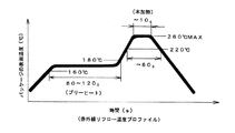
一般にICモジュール樹脂は熱による劣化が生じることが知られている。例えば半田リフローにおけるパッケージクラックはパッケージに吸収された水分とパッケージ樹脂温との関係で生じることが分かっており水分量、温度が高いほど発生しやすくなる。従ってパッケージ水分量及びパッケージ温度をより低く制御することが重要である。ふくれやクラックといった熱ストレスによる現象はすぐに電気的異常を起こすことは稀であるが耐湿特性の劣化を示すことが知られている。これらのことを考慮して図3に示すようにリフロー温度と時間は厳密に管理され、この例ではICパッケージ表面温度の最大温度は260℃/10秒間、220℃以上260℃未満の時間は最大60秒となっている。実際のリフローにおける基板実装の場合は熱による基板の反りによる圧力ストレスも同時に加わるため応力ストレスがない状態ではピーク温度を除く温度条件は緩めに移行すると考えられる。 In general, it is known that IC module resin is deteriorated by heat. For example, it is known that package cracks in solder reflow are caused by the relationship between the moisture absorbed in the package and the package resin temperature, and are more likely to occur as the moisture content and temperature are higher. Therefore, it is important to control the package moisture content and package temperature lower. It is known that phenomena caused by thermal stress such as blisters and cracks rarely cause electrical abnormalities immediately but show deterioration of moisture resistance. In consideration of these points, the reflow temperature and time are strictly controlled as shown in FIG. 3. In this example, the maximum temperature of the IC package surface temperature is 260 ° C./10 seconds, and the time between 220 ° C. and less than 260 ° C. is the maximum. It is 60 seconds. In the case of substrate mounting in actual reflow, pressure stress due to warping of the substrate due to heat is also applied at the same time, so it is considered that the temperature conditions except for the peak temperature shift loosely in the absence of stress stress.
また、一般的なICタグモジュールの樹脂モールドを構成する材料はエポキシ樹脂のような熱硬化性樹脂であり硬化後の熱変形温度は200℃程度となる。高温対応のセラミック封止タイプもあるがコストが高く一般的ではない。この場合の熱変形温度とは一定加重時における規定たわみ量発生温度を示しており素子破壊を示すものではないが、温度管理上のひとつの目安となる。 Moreover, the material which comprises the resin mold of a general IC tag module is a thermosetting resin like an epoxy resin, and the heat deformation temperature after hardening will be about 200 degreeC. There is a ceramic sealing type for high temperatures, but the cost is high and it is not common. The thermal deformation temperature in this case indicates a specified deflection amount generation temperature at a constant load and does not indicate element destruction, but is a guideline for temperature management.
以上を整理すると、ICタグモジュールのパッケージが曝される温度は260℃より低い温度が望ましく、230℃以下がよい、さらに言えば220℃以下がより好適で、200℃以下であればさらに望ましいことになる。また、モジュール内の電子部品の接続において、例えばアンテナとRFIDチップの接続が半田により行われている場合は高融点タイプでも260℃以上では再溶融が発生する。この意味でも260℃以下であることが望ましい。 In summary, the temperature to which the IC tag module package is exposed is preferably lower than 260 ° C, preferably 230 ° C or lower, more preferably 220 ° C or lower, and even more preferably 200 ° C or lower. become. Also, when connecting electronic components in the module, for example, when the antenna and the RFID chip are connected by solder, remelting occurs at 260 ° C. or higher even in the high melting point type. In this sense, the temperature is desirably 260 ° C. or lower.
封止状態での成形材料の温度(成形材料が樹脂単独の場合には樹脂温(封止樹脂温))を230℃以下にするためには該成形材料の融点または溶融温度がそれ以下である必要がある。射出成形機のスクリューシリンダー4及びノズル2の温度(成形温度)と成形材料の温度との差は、成形機の種類によって異なり、又適切な射出圧力は成形体形状及びゲート構造により影響を受け易いことはよく知られている。従って実際の成形封止状態での温度を特定することは困難ではあるが、電子機器筐体などの小型、低重量品では一般的に次のことが言える。すなわち、成形材料はスクリューシリンダー4において溶融され射出されるが成形材料の温度は射出時等のせん断発熱による影響と、成形材料固化のために100℃前後またはそれ以下に設定される金型1の壁面接触による温度低下の影響を受ける。しかし、電子機器筐体などではせん断発熱の影響は小さく金型壁面の影響が大きいためスクリューシリンダー設定温度より成形時の成形材料の温度(樹脂温)は低くなる。
In order to make the temperature of the molding material in the sealed state (resin temperature (sealing resin temperature) when the molding material is a resin alone) 230 ° C. or lower, the melting point or melting temperature of the molding material is lower than that. There is a need. The difference between the temperature (molding temperature) of the screw cylinder 4 and
ただし、金型1内での流動性を確保するために封止するICタグモジュール表面での成形材料温度(樹脂温)は該成形材料の融点または溶融温度以上であることが必要である。従って、成形機や成形体形状などによらず成形時のスクリューシリンダーの温度が成形封止時の成形材料の最高温度、成形材料の融点または溶融温度が成形封止時の成形材料の最低温度と考える。 However, the molding material temperature (resin temperature) on the surface of the IC tag module to be sealed in order to ensure fluidity in the mold 1 needs to be equal to or higher than the melting point or melting temperature of the molding material. Therefore, the temperature of the screw cylinder at the time of molding is the highest temperature of the molding material at the time of molding and the melting point or melting temperature of the molding material is the lowest temperature of the molding material at the time of molding and sealing, regardless of the shape of the molding machine or molded body. Think.
以下に、本発明を検証するために行った実験について説明する。
(実験例1)
実際のICタグモジュールを用いてパッケージダメージとパッケージ表面温度について実験を行った。ここでは、ICタグモジュールとして、大日本印刷株式会社製「Mタグ(ACCUWAVE-IM0505-SLI)」(通信周波数13.56MHz帯のアンテナ一体型、5.45mm角、厚さ750μm)を用い、該ICタグモジュール単体を加熱し樹脂モールドの状態変化及びメモリー機能への影響を評価した。
Below, the experiment conducted in order to verify this invention is demonstrated.
(Experimental example 1)
Experiments were conducted on package damage and package surface temperature using an actual IC tag module. Here, “M tag (ACCUWAVE-IM0505-SLI)” manufactured by Dai Nippon Printing Co., Ltd. (integrated antenna with a communication frequency of 13.56 MHz, 5.45 mm square, thickness 750 μm) is used as the IC tag module. The IC tag module alone was heated to evaluate the change in the state of the resin mold and the effect on the memory function.
本実験では、ICタグモジュールの加熱として常温から150℃まで2℃/秒で昇温し、150℃で2分間保持するプリヒート加熱を行い、ついで150℃からつぎの4通りの加熱を行った。なお本実験においてハロゲンランプによる加熱では昇温過程での保持時間は昇温時間の逆数と定義した。
(加熱条件1)シリコンオイルバスにて230℃まで加熱を行い、230℃で2分間の保温後終了した。
(加熱条件2)ハロゲンランプにより4方向から加熱して5℃/秒で昇温し、目標温度300℃到達で終了した。
(加熱条件3)ハロゲンランプにより4方向から加熱して1℃/秒で昇温し、目標温度300℃到達で終了した。
(加熱条件4)ハロゲンランプにより4方向から加熱して330℃まで昇温し5分間の保温後終了した。
In this experiment, the IC tag module was heated from room temperature to 150 ° C. at a rate of 2 ° C./second, preheated to hold at 150 ° C. for 2 minutes, and then heated from 150 ° C. in the following four ways. In this experiment, the heating time with the halogen lamp was defined as the reciprocal of the temperature rising time during the temperature rising process.
(Heating condition 1) Heating was performed up to 230 ° C. in a silicon oil bath, and the heating was terminated at 230 ° C. for 2 minutes.
(Heating condition 2) Heating was performed in 4 directions with a halogen lamp, the temperature was raised at 5 ° C / second, and the operation was terminated when the target temperature reached 300 ° C.
(Heating condition 3) Heating was performed in 4 directions with a halogen lamp, the temperature was raised at 1 ° C / second, and the operation was terminated when the target temperature reached 300 ° C.
(Heating condition 4) Heating was performed from 4 directions with a halogen lamp, the temperature was raised to 330 ° C., and the heat insulation was completed for 5 minutes.
評価に当っては、加熱中に樹脂モールドの燃焼状態を目視観察し、樹脂モールドの変色、変形については加熱終了後常温に戻ってから目視観察及び寸法測定により行った。また、加熱後のICタグモジュールについて通信によりID読み込み(ID)、書き込み(記録)、書き込んだコードが再生できる状態であるかどうかを評価した。それぞれ可能であれば○、不可であれば×とした。また、読み込み、書き込みはKDRコーポレーション株式会社のKI−730Rを用いた。 In the evaluation, the combustion state of the resin mold was visually observed during heating, and the discoloration and deformation of the resin mold were performed by visual observation and dimension measurement after returning to room temperature after the heating. In addition, the IC tag module after heating was evaluated for ID reading (ID), writing (recording), and whether the written code can be reproduced by communication. Each was marked with ◯ if possible, and x if not possible. For reading and writing, KI-730R manufactured by KDR Corporation was used.
表1に以上の実験結果を示す。
加熱温度230℃では2分間保持しても変色・変形は認められなかった。この結果からパッケージへの熱ダメージを抑えるには射出成形時の成形材料温度(封止樹脂温)を230℃以下にするのが有効であることが分かった。また、加熱条件2において、昇温勾配が5℃/秒(保持0.2秒)と急峻な加熱では加熱温度が295℃と低くなっているのはモジュール内での熱分布が一様ではなく一部分が高くなる影響のためと考えられる。またこの温度は燃焼開始温度であり樹脂そのものは難燃性が付与されているため燃焼続けることはなかった。この結果から300℃前後で燃焼による非可逆なパッケージダメージが生じることが分かった。また、樹脂モールドの変色は黒色化、変形はモジュール厚のふくらみとして観察され最大2%厚みが増した。ただし、通信機能は加熱条件4(加熱温度330℃/5分間保持)以外は、ROM、RAMとも正常に動作することを確認した。従って本実験例でのICタグモジュールのダメージはパッケージクラックと同じように電気的異常が短期的には発生しない信頼性低下現象と考えられる。
Table 1 shows the results of the above experiments.
Even at a heating temperature of 230 ° C. for 2 minutes, no discoloration or deformation was observed. From this result, it was found that it is effective to set the molding material temperature (sealing resin temperature) at the time of injection molding to 230 ° C. or less in order to suppress the thermal damage to the package. In

(実施例1)
ポリ乳酸を主原料とする低融点のプラスチック、ポリスチレン、ポリカーボネートの3種類の成形材料により、成形温度を変えて射出成形を行った。その用いたICタグモジュール及び成形材料は次の通りである。
(1)ICタグモジュール:大日本印刷株式会社製「Mタグ(ACCUWAVE-IM0505-SLI)」(通信周波数13.56MHz帯のアンテナ一体型、5.45mm角、厚さ750μm)
(2)成形材料:つぎの3種類の材料から選択した。
・ポリ乳酸を主原料とする熱可塑性樹脂(三井化学社製:H100J)
・ポリスチレンを主原料とする熱可塑性樹脂(PSジャパン社製:GPPS HF77)
・ポリカーボネートを主原料とする熱可塑性樹脂(帝人化成社製:パンライトL-1225L)
(Example 1)
Injection molding was performed by changing molding temperature using three types of molding materials of low melting point plastic, polystyrene, and polycarbonate mainly composed of polylactic acid. The IC tag module and molding material used are as follows.
(1) IC tag module: “M tag (ACCUWAVE-IM0505-SLI)” manufactured by Dai Nippon Printing Co., Ltd. (integrated antenna with a communication frequency of 13.56 MHz, 5.45 mm square, 750 μm thick)
(2) Molding material: selected from the following three types of materials.
・ Thermoplastic resin mainly made from polylactic acid (Mitsui Chemicals: H100J)
・ Thermoplastic resin mainly made of polystyrene (PS Japan, GPPS HF77)
・ Plastic thermoplastic resin (Teijin Chemicals: Panlite L-1225L)
射出成形に当っては、ICタグモジュールをあらかじめ金型の可動側の水平部に置いた後、金型を閉め、表2に示す成形条件で型締圧50トンの射出成形機(日精樹脂工業製、NEX500)を用いて射出成型を行った。この場合の成形温度は射出成形機のシリンダー設定温度である。なお、成型温度によらず二次圧(保圧)30MPa、射出時間15秒間、冷却時間20秒間一定とした。 In the injection molding, after placing the IC tag module on the horizontal part on the movable side of the mold in advance, the mold is closed, and the injection molding machine with a clamping pressure of 50 tons under the molding conditions shown in Table 2 (Nissei Plastic Industry) NEX500) was used for injection molding. The molding temperature in this case is the cylinder set temperature of the injection molding machine. The secondary pressure (holding pressure) was 30 MPa, the injection time was 15 seconds, and the cooling time was 20 seconds, regardless of the molding temperature.
射出成形により、金型内に置かれたICタグモジュールは成形材料の流動により成形体の端に押しつけられる形で封止され成形体を得た。その後、ICタグモジュールの変形及び通信特性を評価した。
ICタグモジュールの変形を評価するために得られた成型体からICタグモジュールを取り出して厚さを測定した。厚さはマイクロメーターにより測定した。なお、ICタグモジュールの成形材料による封止前の厚さは750μmである。また、通信評価は実験例1の場合と同じ方法で行った。
The IC tag module placed in the mold was sealed by injection molding so as to be pressed against the end of the molded body by the flow of the molding material to obtain a molded body. Thereafter, the deformation and communication characteristics of the IC tag module were evaluated.
The IC tag module was taken out from the molded body obtained for evaluating the deformation of the IC tag module, and the thickness was measured. The thickness was measured with a micrometer. The thickness of the IC tag module before sealing with the molding material is 750 μm. Further, the communication evaluation was performed by the same method as in Experiment Example 1.
表3に評価結果を示す。 Table 3 shows the evaluation results.
成形条件1では、温度と成形圧力によりICタグモジュールのパッケージが厚さ方向の押しつぶされるために厚さがもとの厚さよりも5μm薄くなっている。これに対し成形条件3〜5では加重が加わっているにもかかわらず厚さが厚くなっている。明らかに熱により加重と逆方向の変形であり、成形条件1を基準として反りや膨らみなどの厚さの増加を変形量として規定した。 Under molding condition 1, the package of the IC tag module is crushed in the thickness direction by temperature and molding pressure, so that the thickness is 5 μm thinner than the original thickness. On the other hand, in the molding conditions 3 to 5, the thickness is increased although a weight is applied. Obviously, the deformation was in the direction opposite to the load due to heat, and an increase in thickness such as warpage or swelling was defined as the deformation amount based on the molding condition 1.
また、成形材料による封止におけるICタグモジュールの反りが1%以下で長期信頼性が向上すると考え、厚さが7.5μm以上増加したものは熱によるソリや変形が起こったと判断した。なお、反り1%以下としたのは、日立化成のテクニカルレポート(URL;http://www.hitachi-chem.co.jp/japanease/report/040/40_sou.pdf)において、無鉛半田リフローに対応するための樹脂封止剤の検討が行われているが、ここでは厚さ1.4mmのQFP用封止材としてみた場合のチップ反りについてチップ厚の2%となる30μm以下を設計値としており、この2%の半分の1%以下で長期信頼性が向上すると考えたことによる。 Also, considering that the IC tag module warpage in sealing with a molding material is 1% or less and long-term reliability is improved, it was judged that warp or deformation due to heat occurred when the thickness increased by 7.5 μm or more. The warpage below 1% corresponds to lead-free solder reflow in the Hitachi Chemical Technical Report (URL; http://www.hitachi-chem.co.jp/japanease/report/040/40_sou.pdf) Resin encapsulant has been studied, but here, the design value is 30 μm or less, which is 2% of the chip thickness with respect to the chip warp when viewed as a sealing material for 1.4 mm thick QFP. This is because long-term reliability is improved by 1% or less of half of this 2%.
また、融点(樹脂により融点が存在しないものもあるがここでは樹脂溶融温度も含めて融点として説明している)が164℃及び180℃の低い成形材料を230℃以下の低温成形した成形条件1,2では射出圧の影響があるにもかかわらず1%以上の変形は生じず通信も可能だった。
成形条件3では、成形条件2と同じ樹脂を使い成形温度を260℃と高くして行ったものであり、成形温度が高い分、封止樹脂温が高くなり変形が生じたと考えられる。成形温度は260℃を超えないことが必要であることが分かった。
成形条件4では、融点260℃の成形材料を成形可能なぎりぎりの低い成形温度にて、成形条件5では同じ成形材料を逆に通常より高めの成形温度で行った例である。成形条件4は成形温度が低い分射出圧は高い。どちらも同じように変形が認められた。融点が260℃と高い成形材料を用いる場合は成形条件によらず不適と考えられる。
成形条件3〜5のいずれの場合も短期的には電気的異常は認められず長期信頼性が低下する不良現象であり市場出荷後の不良発生が生じる可能性が高く、ID交換が困難な内蔵型としての使用は困難である。
Further, molding conditions 1 in which a molding material having a low melting point of 164 ° C. and 180 ° C. at a low melting point (230 ° C. or less) is described. 1 and 2 were able to communicate without any deformation of more than 1% despite the influence of injection pressure.
In the molding condition 3, the same resin as in the
The molding condition 4 is an example in which a molding material having a melting point of 260 ° C. is molded at a molding temperature that is as low as possible, and the
In any case of molding conditions 3 to 5, there is a failure phenomenon in which no electrical abnormality is recognized in the short term and long-term reliability is lowered, and there is a high possibility that a failure will occur after shipment from the market. Use as a mold is difficult.
このように、本発明の成形体によって、低融点の脂肪族ポリエステルなどの成形材料を用いて低温一体成形封止することでタグを抜き出すなどの海賊行為に強いIDを商品に付与することが可能となり商品の製造から使用後までの長期間にわたる信頼性の高いIDとしての使用が可能となる。 As described above, the molded article of the present invention can give a product a strong ID against piracy such as extracting a tag by molding and sealing at low temperature using a molding material such as an aliphatic polyester having a low melting point. Therefore, it can be used as a highly reliable ID for a long period from the manufacture of the product to after use.
すなわち、内蔵するICタグモジュールのような電子部品の信頼性を確保するのは例えば樹脂封止により外気と遮断することが望ましいが、本発明では、ICタグモジュールをその電子部品としての信頼性を確保しつつ実際の商品に搭載するために、該ICタグモジュールを特定の成形材料からなる商品筐体などの成形体中に封止している。これによりICタグモジュールの装着のコストが低減されるだけでなく、信頼性やセキュリティを向上させることができる。 That is, in order to ensure the reliability of an electronic component such as a built-in IC tag module, it is desirable to block it from the outside air by, for example, resin sealing, but in the present invention, the reliability of the IC tag module as its electronic component is improved. The IC tag module is sealed in a molded body such as a product casing made of a specific molding material in order to be mounted on an actual product while being secured. This not only reduces the cost of mounting the IC tag module, but also improves reliability and security.
1・・・金型、2・・・ノズル、3・・・スクリュー、4・・・スクリューシリンダー、5・・・ホッパ、6・・・射出シリンダー、7・・・油圧モータ、10・・・光ディスク成形体、11・・・ディスククランプエリア、12・・・記録エリア、13・・・内径部、20・・・ICタグモジュール、22・・・ICチップ DESCRIPTION OF SYMBOLS 1 ... Mold, 2 ... Nozzle, 3 ... Screw, 4 ... Screw cylinder, 5 ... Hopper, 6 ... Injection cylinder, 7 ... Hydraulic motor, 10 ... Optical disk molded body, 11... Disk clamp area, 12... Recording area, 13... Inner diameter portion, 20.
Claims (4)
前記成形材料は、185℃以下の成形温度で射出成形されてなるポリ乳酸を主原料とする熱可塑性樹脂単体または該熱可塑性樹脂を含む材料であることを特徴とする成形体。 An IC tag module integrated with a resin-molded antenna is sealed with a molding material, and is molded into the shape of an optical disc ,
The molding material is a thermoplastic resin alone or a material containing the thermoplastic resin , the main material of which is polylactic acid formed by injection molding at a molding temperature of 185 ° C. or less .
Priority Applications (3)
| Application Number | Priority Date | Filing Date | Title |
|---|---|---|---|
| JP2006212976A JP4200464B2 (en) | 2006-08-04 | 2006-08-04 | Molded body and manufacturing method thereof |
| US11/831,617 US20080057258A1 (en) | 2006-08-04 | 2007-07-31 | Mold body and method of manufacturing the same |
| CNA2007101438687A CN101159105A (en) | 2006-08-04 | 2007-08-03 | Mold body and method of manufacturing the same |
Applications Claiming Priority (1)
| Application Number | Priority Date | Filing Date | Title |
|---|---|---|---|
| JP2006212976A JP4200464B2 (en) | 2006-08-04 | 2006-08-04 | Molded body and manufacturing method thereof |
Publications (2)
| Publication Number | Publication Date |
|---|---|
| JP2008036928A JP2008036928A (en) | 2008-02-21 |
| JP4200464B2 true JP4200464B2 (en) | 2008-12-24 |
Family
ID=39151996
Family Applications (1)
| Application Number | Title | Priority Date | Filing Date |
|---|---|---|---|
| JP2006212976A Expired - Fee Related JP4200464B2 (en) | 2006-08-04 | 2006-08-04 | Molded body and manufacturing method thereof |
Country Status (3)
| Country | Link |
|---|---|
| US (1) | US20080057258A1 (en) |
| JP (1) | JP4200464B2 (en) |
| CN (1) | CN101159105A (en) |
Families Citing this family (8)
| Publication number | Priority date | Publication date | Assignee | Title |
|---|---|---|---|---|
| JP5065833B2 (en) * | 2007-09-28 | 2012-11-07 | 株式会社日立製作所 | RFID tag |
| US8368519B2 (en) * | 2007-10-10 | 2013-02-05 | International Business Machines Corporation | Packaging a semiconductor wafer |
| WO2010054128A2 (en) | 2008-11-05 | 2010-05-14 | Red E Innovations, Llc | Dta holder, system and method |
| JP5375337B2 (en) * | 2009-05-28 | 2013-12-25 | 新日鐵住金株式会社 | Stainless steel seamless pipe manufacturing method |
| DE202010017335U1 (en) | 2010-05-18 | 2011-12-28 | Volker Elsässer | Optical disk disk |
| EP2395507B1 (en) * | 2010-05-18 | 2012-07-25 | Volker Elsässer | Optical data carrier disc |
| US9916778B2 (en) * | 2015-08-06 | 2018-03-13 | Xerox Corporation | Backlighting effect for package displays |
| GB2542361B (en) * | 2015-09-16 | 2021-03-03 | Spa Track Medical Ltd | Method of manufacturing an RFID tag assembly and RFID tag assembly |
-
2006
- 2006-08-04 JP JP2006212976A patent/JP4200464B2/en not_active Expired - Fee Related
-
2007
- 2007-07-31 US US11/831,617 patent/US20080057258A1/en not_active Abandoned
- 2007-08-03 CN CNA2007101438687A patent/CN101159105A/en active Pending
Also Published As
| Publication number | Publication date |
|---|---|
| CN101159105A (en) | 2008-04-09 |
| US20080057258A1 (en) | 2008-03-06 |
| JP2008036928A (en) | 2008-02-21 |
Similar Documents
| Publication | Publication Date | Title |
|---|---|---|
| JP4200464B2 (en) | Molded body and manufacturing method thereof | |
| JP4150015B2 (en) | Totally aromatic liquid crystal polyester resin composition and optical pickup lens holder | |
| EP2258761A1 (en) | Polyester molding for use with a casing | |
| US7645884B2 (en) | Chemical compositions for authenticatable polymers and articles, and authentication methods thereof | |
| Gehring | With radiation crosslinking of engineering plastics into the next millennium | |
| US20120217678A1 (en) | Liquid crystal polyester composition and process for producing the same | |
| JP5312783B2 (en) | Polybutylene terephthalate resin composition | |
| KR20100102539A (en) | Liquid crystalline polyester resin composition and molded article thereof | |
| EP1797556A1 (en) | Marked article and method of making the same | |
| US20100240820A1 (en) | Resin composition and molded product thereof, and method for their production | |
| US20120305178A1 (en) | Anisotropic electrically conductive adhesive film and method for manufacturing same | |
| US20020128344A1 (en) | Biodegradable resin material and method for producing the same | |
| CN103814079A (en) | Polybutylene terephthalate resin composition and welded body | |
| JP5005204B2 (en) | Case, cover or housing molded product that houses electronic components | |
| WO2002094529A1 (en) | Tablet, process for producing the same, and molded article obtained therefrom | |
| JP2006001973A (en) | Polylactic resin composition, molded body and method for fabricating the same, and oa equipment | |
| CN101712791A (en) | Resin composition and resin molded product | |
| JP4847139B2 (en) | Optical disc substrate comprising aromatic polycarbonate resin composition | |
| JP2005298617A (en) | Injection molded product | |
| JP2004176062A (en) | Tablet for optical pickup part, optical pickup part obtained therefrom, and method for preparation of the same | |
| JP2003236944A (en) | Method for manufacturing resin molded product | |
| US20080081210A1 (en) | Authenticatable articles and methods therefor | |
| TWI233936B (en) | Polymer material applied to be signal recording layer of multi-layer information storage medium | |
| JP2006073166A (en) | Optical disk and its manufacturing method | |
| TW200521183A (en) | Component of signal reading apparatus and component of sensor |
Legal Events
| Date | Code | Title | Description |
|---|---|---|---|
| A977 | Report on retrieval |
Free format text: JAPANESE INTERMEDIATE CODE: A971007 Effective date: 20080509 |
|
| A131 | Notification of reasons for refusal |
Free format text: JAPANESE INTERMEDIATE CODE: A131 Effective date: 20080520 |
|
| A521 | Request for written amendment filed |
Free format text: JAPANESE INTERMEDIATE CODE: A523 Effective date: 20080722 |
|
| TRDD | Decision of grant or rejection written | ||
| A01 | Written decision to grant a patent or to grant a registration (utility model) |
Free format text: JAPANESE INTERMEDIATE CODE: A01 Effective date: 20080911 |
|
| A01 | Written decision to grant a patent or to grant a registration (utility model) |
Free format text: JAPANESE INTERMEDIATE CODE: A01 |
|
| A61 | First payment of annual fees (during grant procedure) |
Free format text: JAPANESE INTERMEDIATE CODE: A61 Effective date: 20080924 |
|
| FPAY | Renewal fee payment (event date is renewal date of database) |
Free format text: PAYMENT UNTIL: 20111017 Year of fee payment: 3 |
|
| LAPS | Cancellation because of no payment of annual fees |