JP4198912B2 - Transition structure between symmetric stripline and asymmetric stripline - Google Patents
Transition structure between symmetric stripline and asymmetric stripline Download PDFInfo
- Publication number
- JP4198912B2 JP4198912B2 JP2001504730A JP2001504730A JP4198912B2 JP 4198912 B2 JP4198912 B2 JP 4198912B2 JP 2001504730 A JP2001504730 A JP 2001504730A JP 2001504730 A JP2001504730 A JP 2001504730A JP 4198912 B2 JP4198912 B2 JP 4198912B2
- Authority
- JP
- Japan
- Prior art keywords
- stripline
- transition structure
- section
- asymmetric
- ground plane
- Prior art date
- Legal status (The legal status is an assumption and is not a legal conclusion. Google has not performed a legal analysis and makes no representation as to the accuracy of the status listed.)
- Expired - Lifetime
Links
Images


Classifications
-
- H—ELECTRICITY
- H05—ELECTRIC TECHNIQUES NOT OTHERWISE PROVIDED FOR
- H05K—PRINTED CIRCUITS; CASINGS OR CONSTRUCTIONAL DETAILS OF ELECTRIC APPARATUS; MANUFACTURE OF ASSEMBLAGES OF ELECTRICAL COMPONENTS
- H05K1/00—Printed circuits
- H05K1/02—Details
- H05K1/0213—Electrical arrangements not otherwise provided for
- H05K1/0237—High frequency adaptations
- H05K1/024—Dielectric details, e.g. changing the dielectric material around a transmission line
-
- H—ELECTRICITY
- H01—ELECTRIC ELEMENTS
- H01P—WAVEGUIDES; RESONATORS, LINES, OR OTHER DEVICES OF THE WAVEGUIDE TYPE
- H01P5/00—Coupling devices of the waveguide type
- H01P5/08—Coupling devices of the waveguide type for linking dissimilar lines or devices
-
- H—ELECTRICITY
- H05—ELECTRIC TECHNIQUES NOT OTHERWISE PROVIDED FOR
- H05K—PRINTED CIRCUITS; CASINGS OR CONSTRUCTIONAL DETAILS OF ELECTRIC APPARATUS; MANUFACTURE OF ASSEMBLAGES OF ELECTRICAL COMPONENTS
- H05K1/00—Printed circuits
- H05K1/02—Details
- H05K1/0296—Conductive pattern lay-out details not covered by sub groups H05K1/02 - H05K1/0295
- H05K1/0298—Multilayer circuits
-
- H—ELECTRICITY
- H05—ELECTRIC TECHNIQUES NOT OTHERWISE PROVIDED FOR
- H05K—PRINTED CIRCUITS; CASINGS OR CONSTRUCTIONAL DETAILS OF ELECTRIC APPARATUS; MANUFACTURE OF ASSEMBLAGES OF ELECTRICAL COMPONENTS
- H05K2201/00—Indexing scheme relating to printed circuits covered by H05K1/00
- H05K2201/01—Dielectrics
- H05K2201/0183—Dielectric layers
- H05K2201/0191—Dielectric layers wherein the thickness of the dielectric plays an important role
-
- H—ELECTRICITY
- H05—ELECTRIC TECHNIQUES NOT OTHERWISE PROVIDED FOR
- H05K—PRINTED CIRCUITS; CASINGS OR CONSTRUCTIONAL DETAILS OF ELECTRIC APPARATUS; MANUFACTURE OF ASSEMBLAGES OF ELECTRICAL COMPONENTS
- H05K2201/00—Indexing scheme relating to printed circuits covered by H05K1/00
- H05K2201/07—Electric details
- H05K2201/0707—Shielding
- H05K2201/0715—Shielding provided by an outer layer of PCB
-
- H—ELECTRICITY
- H05—ELECTRIC TECHNIQUES NOT OTHERWISE PROVIDED FOR
- H05K—PRINTED CIRCUITS; CASINGS OR CONSTRUCTIONAL DETAILS OF ELECTRIC APPARATUS; MANUFACTURE OF ASSEMBLAGES OF ELECTRICAL COMPONENTS
- H05K2201/00—Indexing scheme relating to printed circuits covered by H05K1/00
- H05K2201/09—Shape and layout
- H05K2201/09209—Shape and layout details of conductors
- H05K2201/095—Conductive through-holes or vias
- H05K2201/09536—Buried plated through-holes, i.e. plated through-holes formed in a core before lamination
-
- H—ELECTRICITY
- H05—ELECTRIC TECHNIQUES NOT OTHERWISE PROVIDED FOR
- H05K—PRINTED CIRCUITS; CASINGS OR CONSTRUCTIONAL DETAILS OF ELECTRIC APPARATUS; MANUFACTURE OF ASSEMBLAGES OF ELECTRICAL COMPONENTS
- H05K2201/00—Indexing scheme relating to printed circuits covered by H05K1/00
- H05K2201/09—Shape and layout
- H05K2201/09818—Shape or layout details not covered by a single group of H05K2201/09009 - H05K2201/09809
- H05K2201/09845—Stepped hole, via, edge, bump or conductor
Description
【0001】
(発明の分野)
本発明は多層プリント基板、特に多層プリント基板中の対称ストリップと非対称ストリップ線路の間の遷移構造(transition)に関するものである。
【0002】
(発明の背景)
当該技術分野では多くの異なる種類の多層プリント基板が知られている。ここでは一例としてLTCC(低温同時焼成セラミック)を用いて記述するが、他のタイプの多層プリント基板に対しても本発明を適用することができる。
【0003】
簡潔に説明すると、多層プリント基板は以下の方法で製造される。プリント基板設計に基づいて、所要の情報、例えば層数、各層上のパターンの外観および寸法、相異なる層の接触位置などの情報を含む図面が得られる。
【0004】
各層はプラスチックフィルム上にセラミック塊から所定の厚に圧延された層であって、これはテープと呼ばれる。設計にしたがって、これらのテープから互いに異なるパターンが打ち抜かれ、それらは例えば、基板外縁や、層間整合用マーク、いわゆるビアによって異なる層を張り合わせるための穴などのパターンとなる。
【0005】
層を形成した後、ビア穴は適切な導電性材料で埋められる。そして、それぞれの層にパターンが印刷される。ここで導体を正確に位置決めするために共通して用いられるのがスクリーン印刷法である。これらの導体として、金、銀、あるいは他の適切な導電性材料を使用することができる。パターンが定位置に置かれると、それぞれの層が互いに積み重ねられ、すべての層が所定位置に配置される。
【0006】
次に、プリント基板全体が加圧され、直ちにオーブン内において700〜800℃の比較的低い温度(低温)で焼成される(同時焼成)、これにより、セラミック塊が焼結され、セラミックに変性する。このキュアリングすなわち硬化プロセスの後は、テープと呼ばずに、層と呼ぶのが一般的である。
【0007】
高周波信号、特にマイクロ波を使う用途では、許容できないほどの損失と障害が生じるかもしれないので、必ずしも従来の導体を使用できるとは限らない。マイクロ波信号の場合は一般に導体の上側または下側に地板を設ける必要があり、その地板に導体が接続される。導体の片面だけに地板を設けたものは、マイクロストリップと呼ばれる。これらのストリップは通常、一方の面にプリント基板、そして他方の面に空気またはそれに相当する誘電体を備えている。それ以外の場合には、導体が上側と下側の両方の地板で囲まれていることが望ましく、この導体はストリップラインと呼ばれる。導体の両側でストリップラインと地板の間の距離が同じとき、ストリップラインは対称と言われる。これらの距離が互いに異なるとき、ストリップラインは非対称と言われる。
【0008】
対称ストリップラインが最も一般的であるが、非対称ストリップラインが好ましい場合もある。例えば、2つのストリップライン間の距離が長くなるほど、遷移構造の特性が劣化する。その結果、地板に近い非対称ストリップラインと地板の反対側に近い非対称ストリップラインとの間の遷移構造の方が、2つの対称ストリップライン間の遷移構造よりも効果的かもしれない。対称ストリップラインと非対称ストリップライン間の遷移構造は同じ地板の間に形成される場合があり、その基本的なものが図1に示される。
【0009】
ストリップラインを使用する場合の1つの利点は、いわゆるストリップラインモードで例えばマイクロ波帯の信号を送信するとき、導体からの放射が小さいことであり、それがマイクロ波送信にこのような方法がしばしば利用される1つの理由である。マイクロストリップおよびストリップラインは容易に多層プリント基板に形成することができるので、上記理由によりしばしば使用される。地板によって導体を囲むことができるように、導体面と地板は一般にプリント基板内に交互に形成される。
【0010】
多層プリント基板の制作にあたっては、特別な製作ルールに従うことが必要である。例えば、そのようなルールを満たすために、50オームの導体を最小導体幅にするには、与えられた最小厚のテープが必要である。ルールを満たすためには更に、ビアの直径をテープ厚と同等寸法にする必要がある。その結果、図1に示される遷移構造の場合、ビアの直径は非対称ストリップラインの幅よりも大きい。これを補償して、ビアが適切に導体に整合するように誤差マージンを小さく維持するために、通常は導体の一端にカバーパッドを配置する(図2参照)。カバーパッドを配置することにより、ビアと導体の間に不整合が生じる。
【0011】
不整合の問題は低周波数信号の場合には実際に起こらない。しかし、例えばRF信号の場合には不整合が問題となる。一方、導体からの放射が減少するいわゆるストリップラインモードでは普通はRF信号が導通するので、不整合に関連する問題を解決することが望ましい。
【0012】
(発明の概要)
本発明は対称ストリップラインと非対称ストリップライン間の遷移構造の整合性を改善する問題を扱う。
【0013】
したがって、本発明は対称ストリップラインと非対称ストリップライン間の遷移構造を良好にすることを目的とする。
【0014】
要約すれば、本発明は、対称ストリップラインと非対称ストリップライン間の遷移構造に最も近い地板を、ビアの近傍で1レベルの距離だけ遠くに離した構成を提供する。
【0015】
本発明の構成は請求項1記載の特徴を有する。
【0016】
本発明の方法の好ましい実施例は従属請求項2から8に明記される。
【0017】
上記問題に対するこのソリューション一つの利点は、対称ストリップラインと非対称ストリップライン間の遷移構造を改善し得ることであり、これはプリント基板の機能改善および損失軽減を意味する。
【0018】
好ましい実施例と付図にしたがって、以下に発明を詳細に記述する。
【0019】
(好ましい実施例の説明)
図1は対称ストリップラインと非対称ストリップライン間に遷移構造をもつ多層プリント基板の破断図である。参照符号1は互いに積層された複数のキャリア要素、層を表す。層1は、垂直延長部分を示すために破線による分離状態で示される。層1の厚さが均一でないことを理解することができる。図1には発明の理解に必要な数の層だけが示されるが、それより多くの層1が基板に含まれることもある。
【0020】
通常、各層1の少なくとも一部に何らかの導体が設けられる。これらの導体を地板2、10、対称ストリップライン3、非対称ストリップライン4とすることが可能である。通常は、ストリップラインの両側3、4に2つの地板2、10が配置される。図1には地板2、10が1対だけしか示されていないが、複数対の地板を設けることも可能である。
【0021】
前述のように、ストリップライン3を最も近くで取り囲む地板層2、10からストリップラインまでの距離が互いに等しいとき、そのストリップラインは対称と言われる。逆に、この距離が互いに異なるとき、ストリップライン4は非対称と言われる。異なる層における2つのストリップライン、例えば対称ストリップライン3と非対称ストリップライン4を相互接続するために、いわゆるビア5が必要になる。ビア5は少なくとも1層を貫通して延在し、その端部でストリップライン3、4にそれぞれ接続される。
【0022】
しかし、多層プリント基板、例えばLTCCの製作ルールには、導体幅、ビア5のサイズ等に関していくつかの制約がある。例えば50オームの導体の導電幅を最小にするには、層厚を最小にする必要がある。また、製作ルールによればビア5を層1の厚さと同サイズにする必要があるので、それに応じてビア5の直径が定まる。したがって、ビア5の直径が非対称ストリップライン4の幅よりも大になると考えることができる。
【0023】
図2は、非対称ストリップライン4の幅d1を超えるビア径を補償する方法を示しており、この方法により、非対称ストリップライン4にビア5が確実に接続されるように誤差マージンが軽減される。いわゆるカバーパッド6が非対称ストリップライン4の一端に設けられ、このカバーパッド6はビア5に接続される。カバーパッド6の直径d2が非対称ストリップライン4の幅d1を超えると、それらのインピーダンスが異なるので、両者の間で不整合が生じる。不整合の度合いは、カバーパッド6の直径d2と非対称ストリップライン4の幅d1の比q=d1/d2に依存する。サイズの差が大きくなるにしたがって、すなわち、比qが小さくなるにしたがって、カバーパッド6と非対称ストリップライン4間の遷移構造の整合性が悪化する。
【0024】
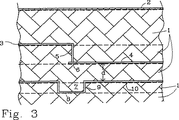
図3は発明の構成を示しており、図1と類似したものである。図1と同様に、図3には複数の層1が示されているが、その数は以下の理由に1つ増えている。2つのストリップライン3、4とビア5は変わらないが、非対称ストリップライン4のカバーパッド6が図示されているところが異なる。ただし、わかり易くするために図2よりも拡大されている。この発明構成では、地板10が非対称ストリップライン4に最も近接するように変更されている。この地板10はカバーパッド6の近傍に凹所7を有する。
【0025】
この凹所7には縦長の溝状地板8と、複数のビア9が含まれ、ビアによって溝状地板8と下側地板10の残余部分とが接続される。ビア9は通常、下側地板10と溝状地板8の両方に対して直角である。最も近い地板10からパッドとストリップラインまでの距離が互いに異なる場合は、カバーパッド6と非対称ストリップライン4間の整合性が改善されるので、それによって凹所7の構造がある程度は定まる。凹所7の構造は、例えば層1の厚さ、導体の線幅、カバーパッド6の構造、地板10から非対称ストリップライン4までの距離(図3のd)、前述の比q等に依存するので、最適設計に関する一般論を述べることはできない。しかし、いくつかの一般的なルールを以下に述べる。ほとんどの場合、凹所7はカバーパッド6の中心に置かれる。通常、凹所7がカバーパッド6の設計を反映することが望ましく、例えば、カバーパッド6の形状が円形、6角形、8角形、または長方形であれば、凹所7も同様の形状になろう。また、凹所7の半径または断面積を大きくし、溝状地板8を遠くに離すこと、すなわち1層以上に相当する距離だけ離すことによって、地板10からカバーパッド6までの距離を長くすることができる。一般に、ストリップライン4の非対称性が増すにしたがって、凹所7からカバーパッド6までの距離は長くなる。
【0026】
凹所7の下側導体面10はカバーパッド6から更に遠くに配置されるので、対称ストリップライン3から非対称ストリップライン4までのビア5による遷移構造の整合性が改善される。それにより、構造全体の性能が向上する。
【0027】
発明は以上の記述および開示実施例に制限されることなく、特許請求の範囲において変更を施すことが可能である。
【図面の簡単な説明】
【図1】 多層プリント基板の破断図であり、対称ストリップラインと非対称のストリップライン間に遷移構造を示す図。
【図2】 導体のカバーパッドとビアの接触状態を示す上面図。
【図3】 図1と類似した発明の構成を示す図であり、ビアとカバーパッドの近傍において地板を局部的に移した状態を示す図。[0001]
(Field of Invention)
The present invention relates to a multilayer printed circuit board, and more particularly to a transition between a symmetric strip and an asymmetric strip line in the multilayer printed circuit board.
[0002]
(Background of the Invention)
Many different types of multilayer printed circuit boards are known in the art. In this example, LTCC (low temperature co-fired ceramic) is used as an example, but the present invention can be applied to other types of multilayer printed boards.
[0003]
Briefly described, the multilayer printed circuit board is manufactured by the following method. Based on the printed circuit board design, a drawing is obtained that contains the required information, such as the number of layers, the appearance and dimensions of the pattern on each layer, the contact positions of the different layers, and the like.
[0004]
Each layer is a layer rolled on a plastic film from a ceramic mass to a predetermined thickness, which is called a tape. According to the design, different patterns are punched from these tapes, and they become, for example, patterns such as the outer edges of the substrate, interlayer alignment marks, so-called holes for bonding different layers by vias.
[0005]
After forming the layer, the via hole is filled with a suitable conductive material. A pattern is printed on each layer. Here, the screen printing method is commonly used to accurately position the conductor. As these conductors, gold, silver, or other suitable conductive materials can be used. When the pattern is in place, the layers are stacked on top of each other and all layers are placed in place.
[0006]
Next, the whole printed circuit board is pressurized and immediately fired in an oven at a relatively low temperature (low temperature) of 700 to 800 ° C. (co-firing), whereby the ceramic mass is sintered and denatured into ceramic. . After this curing or curing process, it is common to refer to layers rather than tapes.
[0007]
In applications using high frequency signals, especially microwaves, conventional conductors may not always be used, as unacceptable loss and failure may occur. In the case of a microwave signal, it is generally necessary to provide a ground plane above or below the conductor, and the conductor is connected to the ground plane. A structure in which a ground plane is provided only on one side of a conductor is called a microstrip. These strips typically comprise a printed circuit board on one side and air or equivalent dielectric on the other side. In other cases, it is desirable for the conductor to be surrounded by both upper and lower ground planes, which is referred to as a stripline. A stripline is said to be symmetric when the distance between the stripline and the ground plane is the same on both sides of the conductor. When these distances are different from each other, the stripline is said to be asymmetric.
[0008]
Symmetric striplines are most common, but asymmetric striplines may be preferred. For example, the longer the distance between two strip lines, the more the characteristics of the transition structure will deteriorate. As a result, a transition structure between an asymmetric stripline near the ground plane and an asymmetric stripline near the opposite side of the ground plane may be more effective than a transition structure between two symmetrical striplines. The transition structure between the symmetric stripline and the asymmetric stripline may be formed between the same ground planes, the basic one of which is shown in FIG.
[0009]
One advantage of using striplines is that when transmitting signals in the microwave band, for example, in so-called stripline mode, the radiation from the conductor is small, which is often the case with such methods for microwave transmission. This is one reason why it is used. Microstrips and striplines are often used for the above reasons because they can be easily formed on multilayer printed circuit boards. The conductor surface and the ground plane are generally formed alternately in the printed circuit board so that the conductor can be surrounded by the ground plane.
[0010]
When producing multilayer printed circuit boards, it is necessary to follow special production rules. For example, to meet such a rule, a given minimum thickness tape is required to bring a 50 ohm conductor to a minimum conductor width. Furthermore, in order to satisfy the rule, the via diameter needs to be the same size as the tape thickness. As a result, for the transition structure shown in FIG. 1, the via diameter is larger than the width of the asymmetric stripline. To compensate for this and to keep the error margin small so that the via is properly aligned with the conductor, a cover pad is usually placed at one end of the conductor (see FIG. 2). By arranging the cover pad, a mismatch occurs between the via and the conductor.
[0011]
The mismatch problem does not actually occur with low frequency signals. However, for example, in the case of an RF signal, mismatch is a problem. On the other hand, in so-called stripline mode, where the radiation from the conductors is reduced, it is usually desirable to solve the problems associated with mismatch because the RF signal is conducted.
[0012]
(Summary of Invention)
The present invention addresses the problem of improving the consistency of transition structures between symmetric and asymmetric striplines.
[0013]
Accordingly, an object of the present invention is to improve the transition structure between a symmetric stripline and an asymmetric stripline.
[0014]
In summary, the present invention provides a configuration in which the ground plane closest to the transition structure between the symmetric stripline and the asymmetric stripline is separated by one level distance near the via.
[0015]
The configuration of the present invention has the features described in claim 1.
[0016]
Preferred embodiments of the method according to the invention are specified in the
[0017]
One advantage of this solution to the above problem is that it can improve the transition structure between the symmetric stripline and the asymmetric stripline, which means improved printed circuit board functionality and reduced loss.
[0018]
The invention is described in detail below in accordance with a preferred embodiment and the accompanying drawings.
[0019]
(Description of the preferred embodiment)
FIG. 1 is a cutaway view of a multilayer printed circuit board having a transition structure between a symmetric stripline and an asymmetric stripline. Reference numeral 1 represents a plurality of carrier elements and layers stacked on each other. Layer 1 is shown separated by a broken line to show a vertical extension. It can be seen that the thickness of layer 1 is not uniform. Although only the number of layers required for understanding the invention is shown in FIG. 1, more layers 1 may be included in the substrate.
[0020]
Usually, some conductor is provided on at least a part of each layer 1. These conductors can be the ground planes 2 and 10, the
[0021]
As described above, a stripline is said to be symmetric when the distances from the ground plane layers 2, 10 that surround the
[0022]
However, the production rules for a multilayer printed circuit board, for example, LTCC, have some restrictions regarding the conductor width, the size of the via 5, and the like. For example, to minimize the conductive width of a 50 ohm conductor, the layer thickness needs to be minimized. Further, according to the production rule, the via 5 needs to have the same size as the thickness of the layer 1, and the diameter of the via 5 is determined accordingly. Therefore, it can be considered that the diameter of the via 5 is larger than the width of the
[0023]
FIG. 2 shows a method for compensating for the via diameter exceeding the width d 1 of the
[0024]
FIG. 3 shows the configuration of the invention, which is similar to FIG. Similar to FIG. 1, a plurality of layers 1 are shown in FIG. 3, but the number is increased by one for the following reasons. The two
[0025]
The recess 7 includes a vertically long groove-like ground plate 8 and a plurality of vias 9, and the groove-like ground plate 8 and the remaining portion of the
[0026]
Since the
[0027]
The invention is not limited to the above description and the disclosed embodiments, but can be modified within the scope of the claims.
[Brief description of the drawings]
FIG. 1 is a cutaway view of a multilayer printed circuit board showing a transition structure between a symmetric stripline and an asymmetric stripline.
FIG. 2 is a top view showing a contact state between a conductor cover pad and a via.
FIG. 3 is a diagram showing a configuration of the invention similar to that of FIG. 1 and showing a state in which a ground plane is locally moved in the vicinity of a via and a cover pad;
Claims (8)
Applications Claiming Priority (3)
| Application Number | Priority Date | Filing Date | Title |
|---|---|---|---|
| SE9902302-0 | 1999-06-17 | ||
| SE9902302A SE514424C2 (en) | 1999-06-17 | 1999-06-17 | Transition between symmetrical and asymmetric stripline in a multilayer PCB |
| PCT/SE2000/001012 WO2000079846A1 (en) | 1999-06-17 | 2000-06-13 | Transition between symmetric stripline and asymmetric stripline |
Publications (3)
| Publication Number | Publication Date |
|---|---|
| JP2003502968A JP2003502968A (en) | 2003-01-21 |
| JP2003502968A5 JP2003502968A5 (en) | 2007-08-02 |
| JP4198912B2 true JP4198912B2 (en) | 2008-12-17 |
Family
ID=20416131
Family Applications (1)
| Application Number | Title | Priority Date | Filing Date |
|---|---|---|---|
| JP2001504730A Expired - Lifetime JP4198912B2 (en) | 1999-06-17 | 2000-06-13 | Transition structure between symmetric stripline and asymmetric stripline |
Country Status (8)
| Country | Link |
|---|---|
| US (1) | US6348844B1 (en) |
| EP (1) | EP1195080B1 (en) |
| JP (1) | JP4198912B2 (en) |
| AU (1) | AU5856900A (en) |
| DE (1) | DE60027297T2 (en) |
| IL (1) | IL146908A (en) |
| SE (1) | SE514424C2 (en) |
| WO (1) | WO2000079846A1 (en) |
Families Citing this family (10)
| Publication number | Priority date | Publication date | Assignee | Title |
|---|---|---|---|---|
| US6483404B1 (en) * | 2001-08-20 | 2002-11-19 | Xytrans, Inc. | Millimeter wave filter for surface mount applications |
| US6873228B1 (en) | 2003-09-30 | 2005-03-29 | National Semiconductor Corporation | Buried self-resonant bypass capacitors within multilayered low temperature co-fired ceramic (LTCC) substrate |
| US6881895B1 (en) | 2003-09-30 | 2005-04-19 | National Semiconductor Corporation | Radio frequency (RF) filter within multilayered low temperature co-fired ceramic (LTCC) substrate |
| US6872962B1 (en) | 2003-09-30 | 2005-03-29 | National Semiconductor Corporation | Radio frequency (RF) filter within multilayered low temperature co-fired ceramic (LTCC) substrate |
| US20050088258A1 (en) * | 2003-10-27 | 2005-04-28 | Xytrans, Inc. | Millimeter wave surface mount filter |
| DE102006047427B4 (en) * | 2006-10-06 | 2012-10-25 | Epcos Ag | Substrate with HF-capable cable |
| DE102007038514A1 (en) * | 2007-08-16 | 2009-02-19 | Robert Bosch Gmbh | Electrical circuit arrangement and method for producing an electrical circuit arrangement |
| US8248183B2 (en) * | 2009-07-30 | 2012-08-21 | Sierra Wireless, Inc. | Circuit board pad having impedance matched to a transmission line and method for providing same |
| GB201113131D0 (en) * | 2011-07-29 | 2011-09-14 | Bae Systems Plc | Radio frequency communication |
| US11342647B2 (en) | 2019-11-26 | 2022-05-24 | Raytheon Company | Free-form dual dual-conductor integrated radio frequency media |
Family Cites Families (3)
| Publication number | Priority date | Publication date | Assignee | Title |
|---|---|---|---|---|
| DE69318879T2 (en) * | 1992-04-03 | 1998-10-08 | Matsushita Electric Ind Co Ltd | Ceramic multi-layer substrate for high frequencies |
| JP3023265B2 (en) * | 1992-09-26 | 2000-03-21 | 日本特殊陶業株式会社 | Package body for integrated circuits |
| JPH06334449A (en) * | 1993-05-25 | 1994-12-02 | Matsushita Electric Ind Co Ltd | Multi-layered board for high frequency amplifier circuit |
-
1999
- 1999-06-17 SE SE9902302A patent/SE514424C2/en unknown
-
2000
- 2000-06-13 JP JP2001504730A patent/JP4198912B2/en not_active Expired - Lifetime
- 2000-06-13 DE DE60027297T patent/DE60027297T2/en not_active Expired - Lifetime
- 2000-06-13 EP EP00944477A patent/EP1195080B1/en not_active Expired - Lifetime
- 2000-06-13 AU AU58569/00A patent/AU5856900A/en not_active Abandoned
- 2000-06-13 IL IL14690800A patent/IL146908A/en not_active IP Right Cessation
- 2000-06-13 WO PCT/SE2000/001012 patent/WO2000079846A1/en active IP Right Grant
- 2000-06-16 US US09/594,771 patent/US6348844B1/en not_active Expired - Lifetime
Also Published As
| Publication number | Publication date |
|---|---|
| JP2003502968A (en) | 2003-01-21 |
| AU5856900A (en) | 2001-01-09 |
| EP1195080B1 (en) | 2006-04-12 |
| WO2000079846A1 (en) | 2000-12-28 |
| SE9902302D0 (en) | 1999-06-17 |
| EP1195080A1 (en) | 2002-04-10 |
| SE514424C2 (en) | 2001-02-19 |
| IL146908A (en) | 2005-11-20 |
| DE60027297T2 (en) | 2007-03-29 |
| DE60027297D1 (en) | 2006-05-24 |
| SE9902302L (en) | 2000-12-18 |
| US6348844B1 (en) | 2002-02-19 |
| IL146908A0 (en) | 2002-08-14 |
Similar Documents
| Publication | Publication Date | Title |
|---|---|---|
| US5982256A (en) | Wiring board equipped with a line for transmitting a high frequency signal | |
| JP3732927B2 (en) | Multilayer wiring board | |
| JP2817487B2 (en) | Chip type directional coupler | |
| US7319370B2 (en) | 180 degrees hybrid coupler | |
| KR940006510B1 (en) | Stripline shielding techniques in low temperature co-fired ceramic | |
| US20070033457A1 (en) | Circuit board and method for manufacturing the same | |
| KR101136423B1 (en) | Circuit board assembly with reduced capacitive coupling | |
| EP0978896B1 (en) | Transmission line and transmission line resonator | |
| JP4198912B2 (en) | Transition structure between symmetric stripline and asymmetric stripline | |
| US6501181B2 (en) | Arrangement relating to electronic circuitry | |
| JP3493265B2 (en) | Dielectric waveguide line and wiring board | |
| JP4278326B2 (en) | Transition between asymmetric stripline and microstrip in a cavity | |
| JPH10135714A (en) | Coupling structure of laminated waveguide lines | |
| JP3347607B2 (en) | Laminated waveguide line | |
| US6917265B2 (en) | Microwave frequency surface mount components and methods of forming same | |
| US8154364B2 (en) | High-frequency transmission line having ground surface patterns with a plurality of notches therein | |
| JPH1174701A (en) | Connection structure for dielectric waveguide line | |
| JP4080981B2 (en) | Conversion circuit | |
| US10511076B2 (en) | RF coupler including vertically stacked coupling sections having conductive layers disposed between the coupling sections and the coupler including a surrounding electric shield | |
| JP4526713B2 (en) | High frequency circuit | |
| KR102608722B1 (en) | Transmission line structure | |
| JP2004104816A (en) | Dielectric waveguide line and wiring board | |
| KR102428983B1 (en) | wave-guide | |
| JPH0716100B2 (en) | Multilayer wiring module | |
| JP2005018627A (en) | Data transfer circuit board |
Legal Events
| Date | Code | Title | Description |
|---|---|---|---|
| RD03 | Notification of appointment of power of attorney |
Free format text: JAPANESE INTERMEDIATE CODE: A7423 Effective date: 20060411 |
|
| RD05 | Notification of revocation of power of attorney |
Free format text: JAPANESE INTERMEDIATE CODE: A7425 Effective date: 20060629 |
|
| A521 | Request for written amendment filed |
Free format text: JAPANESE INTERMEDIATE CODE: A523 Effective date: 20070613 |
|
| A621 | Written request for application examination |
Free format text: JAPANESE INTERMEDIATE CODE: A621 Effective date: 20070613 |
|
| A977 | Report on retrieval |
Free format text: JAPANESE INTERMEDIATE CODE: A971007 Effective date: 20080812 |
|
| TRDD | Decision of grant or rejection written | ||
| A01 | Written decision to grant a patent or to grant a registration (utility model) |
Free format text: JAPANESE INTERMEDIATE CODE: A01 Effective date: 20080908 |
|
| A01 | Written decision to grant a patent or to grant a registration (utility model) |
Free format text: JAPANESE INTERMEDIATE CODE: A01 |
|
| A61 | First payment of annual fees (during grant procedure) |
Free format text: JAPANESE INTERMEDIATE CODE: A61 Effective date: 20081002 |
|
| FPAY | Renewal fee payment (event date is renewal date of database) |
Free format text: PAYMENT UNTIL: 20111010 Year of fee payment: 3 |
|
| R150 | Certificate of patent or registration of utility model |
Ref document number: 4198912 Country of ref document: JP Free format text: JAPANESE INTERMEDIATE CODE: R150 Free format text: JAPANESE INTERMEDIATE CODE: R150 |
|
| FPAY | Renewal fee payment (event date is renewal date of database) |
Free format text: PAYMENT UNTIL: 20121010 Year of fee payment: 4 |
|
| R250 | Receipt of annual fees |
Free format text: JAPANESE INTERMEDIATE CODE: R250 |
|
| FPAY | Renewal fee payment (event date is renewal date of database) |
Free format text: PAYMENT UNTIL: 20131010 Year of fee payment: 5 |
|
| R250 | Receipt of annual fees |
Free format text: JAPANESE INTERMEDIATE CODE: R250 |
|
| R250 | Receipt of annual fees |
Free format text: JAPANESE INTERMEDIATE CODE: R250 |
|
| R250 | Receipt of annual fees |
Free format text: JAPANESE INTERMEDIATE CODE: R250 |
|
| R250 | Receipt of annual fees |
Free format text: JAPANESE INTERMEDIATE CODE: R250 |
|
| R250 | Receipt of annual fees |
Free format text: JAPANESE INTERMEDIATE CODE: R250 |
|
| R250 | Receipt of annual fees |
Free format text: JAPANESE INTERMEDIATE CODE: R250 |
|
| R250 | Receipt of annual fees |
Free format text: JAPANESE INTERMEDIATE CODE: R250 |
|
| R250 | Receipt of annual fees |
Free format text: JAPANESE INTERMEDIATE CODE: R250 |
|
| EXPY | Cancellation because of completion of term |