EP1195080B1 - Transition between symmetric stripline and asymmetric stripline - Google Patents
Transition between symmetric stripline and asymmetric stripline Download PDFInfo
- Publication number
- EP1195080B1 EP1195080B1 EP00944477A EP00944477A EP1195080B1 EP 1195080 B1 EP1195080 B1 EP 1195080B1 EP 00944477 A EP00944477 A EP 00944477A EP 00944477 A EP00944477 A EP 00944477A EP 1195080 B1 EP1195080 B1 EP 1195080B1
- Authority
- EP
- European Patent Office
- Prior art keywords
- stripline
- section
- asymmetric
- transition
- symmetric
- Prior art date
- Legal status (The legal status is an assumption and is not a legal conclusion. Google has not performed a legal analysis and makes no representation as to the accuracy of the status listed.)
- Expired - Lifetime
Links
Images
Classifications
-
- H—ELECTRICITY
- H05—ELECTRIC TECHNIQUES NOT OTHERWISE PROVIDED FOR
- H05K—PRINTED CIRCUITS; CASINGS OR CONSTRUCTIONAL DETAILS OF ELECTRIC APPARATUS; MANUFACTURE OF ASSEMBLAGES OF ELECTRICAL COMPONENTS
- H05K1/00—Printed circuits
- H05K1/02—Details
- H05K1/0213—Electrical arrangements not otherwise provided for
- H05K1/0237—High frequency adaptations
- H05K1/024—Dielectric details, e.g. changing the dielectric material around a transmission line
-
- H—ELECTRICITY
- H01—ELECTRIC ELEMENTS
- H01P—WAVEGUIDES; RESONATORS, LINES, OR OTHER DEVICES OF THE WAVEGUIDE TYPE
- H01P5/00—Coupling devices of the waveguide type
- H01P5/08—Coupling devices of the waveguide type for linking dissimilar lines or devices
-
- H—ELECTRICITY
- H05—ELECTRIC TECHNIQUES NOT OTHERWISE PROVIDED FOR
- H05K—PRINTED CIRCUITS; CASINGS OR CONSTRUCTIONAL DETAILS OF ELECTRIC APPARATUS; MANUFACTURE OF ASSEMBLAGES OF ELECTRICAL COMPONENTS
- H05K1/00—Printed circuits
- H05K1/02—Details
- H05K1/0296—Conductive pattern lay-out details not covered by sub groups H05K1/02 - H05K1/0295
- H05K1/0298—Multilayer circuits
-
- H—ELECTRICITY
- H05—ELECTRIC TECHNIQUES NOT OTHERWISE PROVIDED FOR
- H05K—PRINTED CIRCUITS; CASINGS OR CONSTRUCTIONAL DETAILS OF ELECTRIC APPARATUS; MANUFACTURE OF ASSEMBLAGES OF ELECTRICAL COMPONENTS
- H05K2201/00—Indexing scheme relating to printed circuits covered by H05K1/00
- H05K2201/01—Dielectrics
- H05K2201/0183—Dielectric layers
- H05K2201/0191—Dielectric layers wherein the thickness of the dielectric plays an important role
-
- H—ELECTRICITY
- H05—ELECTRIC TECHNIQUES NOT OTHERWISE PROVIDED FOR
- H05K—PRINTED CIRCUITS; CASINGS OR CONSTRUCTIONAL DETAILS OF ELECTRIC APPARATUS; MANUFACTURE OF ASSEMBLAGES OF ELECTRICAL COMPONENTS
- H05K2201/00—Indexing scheme relating to printed circuits covered by H05K1/00
- H05K2201/07—Electric details
- H05K2201/0707—Shielding
- H05K2201/0715—Shielding provided by an outer layer of PCB
-
- H—ELECTRICITY
- H05—ELECTRIC TECHNIQUES NOT OTHERWISE PROVIDED FOR
- H05K—PRINTED CIRCUITS; CASINGS OR CONSTRUCTIONAL DETAILS OF ELECTRIC APPARATUS; MANUFACTURE OF ASSEMBLAGES OF ELECTRICAL COMPONENTS
- H05K2201/00—Indexing scheme relating to printed circuits covered by H05K1/00
- H05K2201/09—Shape and layout
- H05K2201/09209—Shape and layout details of conductors
- H05K2201/095—Conductive through-holes or vias
- H05K2201/09536—Buried plated through-holes, i.e. plated through-holes formed in a core before lamination
-
- H—ELECTRICITY
- H05—ELECTRIC TECHNIQUES NOT OTHERWISE PROVIDED FOR
- H05K—PRINTED CIRCUITS; CASINGS OR CONSTRUCTIONAL DETAILS OF ELECTRIC APPARATUS; MANUFACTURE OF ASSEMBLAGES OF ELECTRICAL COMPONENTS
- H05K2201/00—Indexing scheme relating to printed circuits covered by H05K1/00
- H05K2201/09—Shape and layout
- H05K2201/09818—Shape or layout details not covered by a single group of H05K2201/09009 - H05K2201/09809
- H05K2201/09845—Stepped hole, via, edge, bump or conductor
Definitions
- the present invention relates to multilayer printed circuit boards, and more specifically to a transition between symmetric and asymmetric striplines in such boards.
- LTCC Low Temperature Co-fired Ceramic
- multilayer printed circuit boards are manufactured in the following way. There is obtained on the basis of a printed circuit board design a drawing that contains necessary information, such as the number of layers, the appearance and dimensions of the patterns on the various layers, the locations at which different layers shall contact one another, and so on.
- Each layer per se is rolled out from a ceramic mass to a predetermined thickness on a plastic film; this is a so-called tape.
- Different patterns are punched from these tapes in accordance with the design; among other things, the outer edges of the board, the marks that are later used to match the layers together, and holes for binding different layers together with so-called vias.
- the via holes are filled with a suitable conductive material.
- the patterns are then printed on each of the layers.
- a common method in this respect is to use screen printing to correctly position the conductors. These conductors may consist of gold, silver or some other suitable conductive material.
- the whole of the printed circuit board is then placed under pressure, inserted into an oven and baked immediately (Co-fired) at a relatively low temperature, 700-800 degrees centigrade (Low Temperature), wherewith the ceramic mass is sintered and transformed to a ceramic. Subsequent to this curing or hardening process, it is usual to speak of layers instead of tapes.
- a normal requirement in the case of microwave signals is the presence of an earth plane above or beneath a conductor, this earth plane following the conductor.
- a conductor only has an earth plane on one side it is called a microstrip.
- These strips are normally arranged so that they have the printed circuit board on one side and air or a corresponding dielectric on the other side.
- it is desirable that the conductor is surrounded by both an upper and a lower earth plane, this conductor then being called a stripline.
- the stripline is symmetrical.
- the stripline is said to be asymmetrical.
- symmetric striplines are the most common, there are occasions when an asymmetric stripline is preferred; for instance, the performance of a transition becomes poorer the greater the distance between the two striplines. Consequently, a transition between an asymmetric stripline close to an earth plane to an asymmetric stripline that is close to the other side of the earth plane may be more effective than a transition between two symmetric striplines.
- the transition between symmetric and asymmetric striplines is sometimes made between the same earth planes, which, in principle, is what is shown in Figure 1.
- striplines One advantage afforded by striplines is that radiation from the conductors is small when, e.g., transmitting signals in the microwave range in so-called stripline-mode, which is one reason why such signals are often transmitted in this way.
- Microstrips and striplines can be easily provided in multilayer printed circuit boards, and are consequently often used to this end. In order to enable conductors to be surrounded by earth planes, conductor planes and earth planes are normally disposed alternately in the printed circuit board.
- Mismatch problems do not actually occur in the case of low frequency signals. Mismatch, however, is a problem in the case of RF signals, for instance. Because it is otherwise usual to conduct RF signals in a so-called stripline mode, which reduces radiation from the conductors, it is desirable to solve problems associated with mismatching.
- the present invention addresses the problem of improving matching in the transition between a symmetric and an asymmetric stripline.
- one object of the present invention is to provide a transition between symmetric and asymmetric striplines that results in good matching.
- the present invention provides an arrangement with a transition between a symmetric an asymmetric stripline in which the earth plane closest to the transition is moved away through the distance of one level in the proximity of the via.
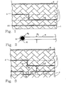
- Figure 1 is a cut-away view of a multilayer printed circuit board having a transition between a symmetric and an asymmetric stripline.
- Reference numeral 1 identifies a number of mutually stacked carrier elements, layers. The layers 1 are shown separated by broken lines, in order to illustrate their vertical extension. It will be seen that the layers 1 have different thicknesses.
- the board may also include more layers 1 than those illustrated in Figure 1, in which only those layers necessary for an understanding of the invention have been shown.
- a conductor of some kind normally lies on at least part of each layer 1.
- These conductors may be earth planes 2, 10, symmetric striplines 3 and asymmetric striplines 4.
- Normally, two earth planes 2, 10 are placed on respective sides of a stripline 3, 4.
- Figure 1 shows only one pair of earth planes 2, 10, the earth planes will often be more in number.
- a stripline 3 is said to be symmetrical when the distances to the nearest surrounding earth layers 2, 10 are mutually the same.
- the stripline 4 is said to be asymmetric when these distances are different.
- a so-called via 5 is required to interconnect two striplines in different layers, for instance to connect a symmetric stripline 3 withy an asymmetric stripline 4.
- the via 5 extends through at least one layer and connects at each end to a stripline 3, 4.
- the construction rules for multilayer printed circuit boards have certain restrictions with respect to conductor width, sizes of vias 5, etc.
- a given smallest conductive width for, e.g., a 50-ohm conductor requires a given smallest layer thickness.
- the rules also require the vias 5 to have the same size as the thickness of the layer 1, this determines, in turn, the diameter of the vias 5. This can mean that the diameter of the via 5 will be greater than the width of the asymmetric stripline 4.
- Figure 2 illustrates a method of compensating for a via diameter that is greater than the width d 1 of the asymmetric stripline 4, this method also providing a small error margin that will ensure that the via 5 is safely connected to the asymmetric stripline 4.
- One end of the asymmetric stripline 4 is provided with a so-called coverpad 6 which is placed so that the via 5 connects with the coverpad 6.
- coverpad 6 which is placed so that the via 5 connects with the coverpad 6.
- Figure 3 is a view similar to Figure 1 illustrating the inventive arrangement. Similar to Figure 1, Figure 3 illustrates a number of layers 1, these layers being one more than earlier mentioned for the reason given below.
- the two striplines 3, 4 and the via 5 are unchanged, with the exception that the coverpad 6 of the asymmetric stripline 4 has been shown, enlarged in comparison with Figure 2 for the sake of illustration.
- the inventive arrangement involves an alteration to the earth plane 10 that is located closest to the asymmetric stripline 4. This earth plane 10 has a recessed part 7 in the vicinity of the coverpad 6.
- This recessed part 7 includes a longitudinally extending recessed earth plane 8, and a number of vias 9 which connect the recessed earth plane 8 with the remainder of the lower earth plane 10.
- the vias 9 are generally perpendicular to both the lower earth plane 10 and the recessed earth plane 8. Because the match between cover pad 6 and asymmetric stripline 4 is improved when said pad and stripline are located at different distances from the nearest earth plane 10, this determines the construction of the recess part 7 to some extent.
- the recessed part 7 is most often centred on the centre point of the coverpad 6. Normally, it is desirable that the recessed part 7 reflects the design of the cover pad 6; for instance, when the coverpad 6 has a circular, hexagonal, octagonal or rectangular shape, the recessed part 7 will also be given a similar shape.
- the distance of the coverpad 6 from the earth plane 10 can be increased both by increasing the radius or cross-dimension of the recessed part 7 and by placing the recessed earth plane 8 further away, i.e. through a distance corresponding to more than one layer. Normally, the more asymmetric the stripline 4 the greater the distance of the coverpad 6 from the recessed part 7.
Landscapes
- Engineering & Computer Science (AREA)
- Microelectronics & Electronic Packaging (AREA)
- Production Of Multi-Layered Print Wiring Board (AREA)
- Structure Of Printed Boards (AREA)
- Waveguide Connection Structure (AREA)
Abstract
Description
- The present invention relates to multilayer printed circuit boards, and more specifically to a transition between symmetric and asymmetric striplines in such boards.
- Many different sorts of multilayer printed circuit boards are known to the art. LTCC (Low Temperature Co-fired Ceramic) will be used hereinafter as an example, although it will be understood that the invention can also be applied in other types of multilayer printed circuit boards.
- Briefly, multilayer printed circuit boards are manufactured in the following way. There is obtained on the basis of a printed circuit board design a drawing that contains necessary information, such as the number of layers, the appearance and dimensions of the patterns on the various layers, the locations at which different layers shall contact one another, and so on.
- Each layer per se is rolled out from a ceramic mass to a predetermined thickness on a plastic film; this is a so-called tape. Different patterns are punched from these tapes in accordance with the design; among other things, the outer edges of the board, the marks that are later used to match the layers together, and holes for binding different layers together with so-called vias.
- Subsequent to configuring the layers, the via holes are filled with a suitable conductive material. The patterns are then printed on each of the layers. A common method in this respect is to use screen printing to correctly position the conductors. These conductors may consist of gold, silver or some other suitable conductive material. When the patterns are in place, the various layers are placed one upon the other until all layers are in position.
- The whole of the printed circuit board is then placed under pressure, inserted into an oven and baked immediately (Co-fired) at a relatively low temperature, 700-800 degrees centigrade (Low Temperature), wherewith the ceramic mass is sintered and transformed to a ceramic. Subsequent to this curing or hardening process, it is usual to speak of layers instead of tapes.
- In the case of applications for high frequency signals, particularly within the microwave field, it is not always possible to use traditional conductors, since this would result in unacceptable losses and disturbances. A normal requirement in the case of microwave signals is the presence of an earth plane above or beneath a conductor, this earth plane following the conductor. When a conductor only has an earth plane on one side it is called a microstrip. These strips are normally arranged so that they have the printed circuit board on one side and air or a corresponding dielectric on the other side. In other cases, it is desirable that the conductor is surrounded by both an upper and a lower earth plane, this conductor then being called a stripline. When the distances between a stripline and the earth planes are the same on both sides of the conductor, it is said that the stripline is symmetrical. When these distances are mutually different, the stripline is said to be asymmetrical.
- Although symmetric striplines are the most common, there are occasions when an asymmetric stripline is preferred; for instance, the performance of a transition becomes poorer the greater the distance between the two striplines. Consequently, a transition between an asymmetric stripline close to an earth plane to an asymmetric stripline that is close to the other side of the earth plane may be more effective than a transition between two symmetric striplines. The transition between symmetric and asymmetric striplines is sometimes made between the same earth planes, which, in principle, is what is shown in Figure 1.
- One advantage afforded by striplines is that radiation from the conductors is small when, e.g., transmitting signals in the microwave range in so-called stripline-mode, which is one reason why such signals are often transmitted in this way. Microstrips and striplines can be easily provided in multilayer printed circuit boards, and are consequently often used to this end. In order to enable conductors to be surrounded by earth planes, conductor planes and earth planes are normally disposed alternately in the printed circuit board.
- It is necessary to follow special construction rules in the production of multilayer printed circuit boards. For instance, in order to satisfy the rules a given smallest tape thickness is required for a smallest conductor width of a 50-ohm conductor. The rules also require the diameter of the vias to be in the same order of magnitude as the thickness of the tape. Consequently, in the case of the transition shown in Figure 1, the diameter of the via is greater than the width of the asymmetric stripline. In order to compensate for this and to ensure only a small margin of error so that the via will safely meet the conductor, it is normal to place a cover pad on one end of the conductor; see Figure 2. The presence of the cover pad results in a mismatch between the via and the conductor.
- Mismatch problems do not actually occur in the case of low frequency signals. Mismatch, however, is a problem in the case of RF signals, for instance. Because it is otherwise usual to conduct RF signals in a so-called stripline mode, which reduces radiation from the conductors, it is desirable to solve problems associated with mismatching.
- The present invention addresses the problem of improving matching in the transition between a symmetric and an asymmetric stripline.
- Accordingly, one object of the present invention is to provide a transition between symmetric and asymmetric striplines that results in good matching.
- In brief, the present invention provides an arrangement with a transition between a symmetric an asymmetric stripline in which the earth plane closest to the transition is moved away through the distance of one level in the proximity of the via.
- The invention arrangement is characterised by the features set forth in the accompanying
Claim 1. - Advantageous embodiments of the inventive method will be evident from the dependent Claims 2-8.
- One advantage with this solution to the problem is that transitions between symmetric and asymmetric striplines can be made with better matching, meaning that the printed circuit board will perform better and have less losses.
- The invention will now be described in more detail with reference to preferred embodiments thereof and also with reference to the accompanying drawing.
-
- Figure 1 is a cut-away view of a multilayer printed circuit board and shows a transition between a symmetric and an asymmetric stripline.
- Figure 2 shows how a via meets the cover pad of a conductor, as seen from above.
- Figure 3 is a view similar to the view of Figure 1 showing the inventive arrangement, i.e. local movement of the earth plane in the proximity of the via and the cover pad.
- Figure 1 is a cut-away view of a multilayer printed circuit board having a transition between a symmetric and an asymmetric stripline.
Reference numeral 1 identifies a number of mutually stacked carrier elements, layers. Thelayers 1 are shown separated by broken lines, in order to illustrate their vertical extension. It will be seen that thelayers 1 have different thicknesses. The board may also includemore layers 1 than those illustrated in Figure 1, in which only those layers necessary for an understanding of the invention have been shown. - A conductor of some kind normally lies on at least part of each
layer 1. These conductors may beearth planes symmetric striplines 3 andasymmetric striplines 4. Normally, twoearth planes stripline earth planes - As earlier mentioned, a
stripline 3 is said to be symmetrical when the distances to the nearest surroundingearth layers stripline 4 is said to be asymmetric when these distances are different. A so-called via 5 is required to interconnect two striplines in different layers, for instance to connect asymmetric stripline 3 withy anasymmetric stripline 4. Thevia 5 extends through at least one layer and connects at each end to astripline - However, the construction rules for multilayer printed circuit boards, for instance LTCC, have certain restrictions with respect to conductor width, sizes of
vias 5, etc. A given smallest conductive width for, e.g., a 50-ohm conductor requires a given smallest layer thickness. As the rules also require thevias 5 to have the same size as the thickness of thelayer 1, this determines, in turn, the diameter of thevias 5. This can mean that the diameter of the via 5 will be greater than the width of theasymmetric stripline 4. - Figure 2 illustrates a method of compensating for a via diameter that is greater than the width d1 of the
asymmetric stripline 4, this method also providing a small error margin that will ensure that the via 5 is safely connected to theasymmetric stripline 4. One end of theasymmetric stripline 4 is provided with a so-calledcoverpad 6 which is placed so that the via 5 connects with thecoverpad 6. When the diameter d2 of thecoverpad 6 is greater than the width d1 of theasymmetric stripline 4, a mismatch occurs therebetween, since their impedances are different. The degree of mismatch is dependent on the quotient q=d1/d2 between the diameter d2 of thecover pad 6 and the width d1 of theasymmetric stripline 4. The greater this difference in size, i.e. the smaller that q is, the poorer the match in the transition betweencoverpad 6 andasymmetric stripline 4. - Figure 3 is a view similar to Figure 1 illustrating the inventive arrangement. Similar to Figure 1, Figure 3 illustrates a number of
layers 1, these layers being one more than earlier mentioned for the reason given below. The twostriplines coverpad 6 of theasymmetric stripline 4 has been shown, enlarged in comparison with Figure 2 for the sake of illustration. The inventive arrangement involves an alteration to theearth plane 10 that is located closest to theasymmetric stripline 4. Thisearth plane 10 has a recessed part 7 in the vicinity of thecoverpad 6. - This recessed part 7 includes a longitudinally extending recessed
earth plane 8, and a number ofvias 9 which connect the recessedearth plane 8 with the remainder of thelower earth plane 10. Thevias 9 are generally perpendicular to both thelower earth plane 10 and the recessedearth plane 8. Because the match betweencover pad 6 andasymmetric stripline 4 is improved when said pad and stripline are located at different distances from thenearest earth plane 10, this determines the construction of the recess part 7 to some extent. A general description of an optimal design cannot be given, because the construction of the recessed part 7 is dependent on the thickness of thelayers 1, the line width of the conductors, the construction of thecoverpad 6, the distance of theasymmetric stripline 4 from the earth plane 10 (d in Figure 3) and the aforesaid quotient q among other things. However, some general rules will be given hereinafter. The recessed part 7 is most often centred on the centre point of thecoverpad 6. Normally, it is desirable that the recessed part 7 reflects the design of thecover pad 6; for instance, when thecoverpad 6 has a circular, hexagonal, octagonal or rectangular shape, the recessed part 7 will also be given a similar shape. Furthermore, the distance of thecoverpad 6 from theearth plane 10 can be increased both by increasing the radius or cross-dimension of the recessed part 7 and by placing the recessedearth plane 8 further away, i.e. through a distance corresponding to more than one layer. Normally, the more asymmetric thestripline 4 the greater the distance of thecoverpad 6 from the recessed part 7. - Because the
lower conductor plane 10 in the recessed part 7 is located further away from thecoverpad 6, an improvement is achieved in the match in the transition with the via 5 from thesymmetric stripline 3 to theasymmetric stripline 4. This enhances the performance of the entire construction. - It will be understood that invention is not restricted to the described and illustrated embodiments thereof, and that modifications can be made within the scope of the accompanying Claims.
Claims (8)
- A transition between a symmetric stripline (3) and an asymmetric stripline (4) in which the via (5) between said striplines (3, 4) connects with a coverpad (6) connected to one end of the asymmetric stripline (4), characterised in that an earth plane (10), which is located nearest the asymmetric stripline (4), includes around the extension of the via (5) in a direction towards said earth plane (10), a section (7) that is located further away from the asymmetric stripline (4) than the remainder of said earth plane (10) by a number of layers (1).
- A transition according to Claim 1, characterised in that said section (7) is configured so that its shape in the longitudinal direction of the layers (1) will be essentially the same as the shape of the coverpad (6) in said direction.
- A transition according to Claim 2, characterised in that the section (7) has a circular cross-section.
- A transition according to Claim 2, characterised in that the section (7) has an hexagonal cross-section.
- A transition according to Claim 2, characterised in that the section (7) has an octagonal cross-section.
- A transition according to Claim 2, characterised in that the section (7) has a rectangular cross-section.
- A transition according to Claim 1, characterised in that said section (7) includes a bottom part (8) and a number of vias (9) that extend generally perpendicularly to said bottom part (8) and which place the bottom part (8) in electrical contact with the earth plane (10).
- A transition according to Claims 1-2, characterised in that said section (7) is centred on the centre point of the coverpad (6).
Applications Claiming Priority (3)
| Application Number | Priority Date | Filing Date | Title |
|---|---|---|---|
| SE9902302A SE514424C2 (en) | 1999-06-17 | 1999-06-17 | Transition between symmetrical and asymmetric stripline in a multilayer PCB |
| SE9902302 | 1999-06-17 | ||
| PCT/SE2000/001012 WO2000079846A1 (en) | 1999-06-17 | 2000-06-13 | Transition between symmetric stripline and asymmetric stripline |
Publications (2)
| Publication Number | Publication Date |
|---|---|
| EP1195080A1 EP1195080A1 (en) | 2002-04-10 |
| EP1195080B1 true EP1195080B1 (en) | 2006-04-12 |
Family
ID=20416131
Family Applications (1)
| Application Number | Title | Priority Date | Filing Date |
|---|---|---|---|
| EP00944477A Expired - Lifetime EP1195080B1 (en) | 1999-06-17 | 2000-06-13 | Transition between symmetric stripline and asymmetric stripline |
Country Status (8)
| Country | Link |
|---|---|
| US (1) | US6348844B1 (en) |
| EP (1) | EP1195080B1 (en) |
| JP (1) | JP4198912B2 (en) |
| AU (1) | AU5856900A (en) |
| DE (1) | DE60027297T2 (en) |
| IL (1) | IL146908A (en) |
| SE (1) | SE514424C2 (en) |
| WO (1) | WO2000079846A1 (en) |
Families Citing this family (10)
| Publication number | Priority date | Publication date | Assignee | Title |
|---|---|---|---|---|
| US6483404B1 (en) * | 2001-08-20 | 2002-11-19 | Xytrans, Inc. | Millimeter wave filter for surface mount applications |
| US6873228B1 (en) | 2003-09-30 | 2005-03-29 | National Semiconductor Corporation | Buried self-resonant bypass capacitors within multilayered low temperature co-fired ceramic (LTCC) substrate |
| US6881895B1 (en) | 2003-09-30 | 2005-04-19 | National Semiconductor Corporation | Radio frequency (RF) filter within multilayered low temperature co-fired ceramic (LTCC) substrate |
| US6872962B1 (en) | 2003-09-30 | 2005-03-29 | National Semiconductor Corporation | Radio frequency (RF) filter within multilayered low temperature co-fired ceramic (LTCC) substrate |
| US20050088258A1 (en) * | 2003-10-27 | 2005-04-28 | Xytrans, Inc. | Millimeter wave surface mount filter |
| DE102006047427B4 (en) * | 2006-10-06 | 2012-10-25 | Epcos Ag | Substrate with HF-capable cable |
| DE102007038514A1 (en) * | 2007-08-16 | 2009-02-19 | Robert Bosch Gmbh | Electrical circuit arrangement and method for producing an electrical circuit arrangement |
| US8248183B2 (en) * | 2009-07-30 | 2012-08-21 | Sierra Wireless, Inc. | Circuit board pad having impedance matched to a transmission line and method for providing same |
| GB201113131D0 (en) * | 2011-07-29 | 2011-09-14 | Bae Systems Plc | Radio frequency communication |
| US11342647B2 (en) | 2019-11-26 | 2022-05-24 | Raytheon Company | Free-form dual dual-conductor integrated radio frequency media |
Family Cites Families (3)
| Publication number | Priority date | Publication date | Assignee | Title |
|---|---|---|---|---|
| DE69318879T2 (en) * | 1992-04-03 | 1998-10-08 | Matsushita Electric Ind Co Ltd | Ceramic multi-layer substrate for high frequencies |
| JP3023265B2 (en) * | 1992-09-26 | 2000-03-21 | 日本特殊陶業株式会社 | Package body for integrated circuits |
| JPH06334449A (en) * | 1993-05-25 | 1994-12-02 | Matsushita Electric Ind Co Ltd | Multi-layered board for high frequency amplifier circuit |
-
1999
- 1999-06-17 SE SE9902302A patent/SE514424C2/en unknown
-
2000
- 2000-06-13 AU AU58569/00A patent/AU5856900A/en not_active Abandoned
- 2000-06-13 JP JP2001504730A patent/JP4198912B2/en not_active Expired - Lifetime
- 2000-06-13 IL IL14690800A patent/IL146908A/en not_active IP Right Cessation
- 2000-06-13 EP EP00944477A patent/EP1195080B1/en not_active Expired - Lifetime
- 2000-06-13 WO PCT/SE2000/001012 patent/WO2000079846A1/en active IP Right Grant
- 2000-06-13 DE DE60027297T patent/DE60027297T2/en not_active Expired - Lifetime
- 2000-06-16 US US09/594,771 patent/US6348844B1/en not_active Expired - Lifetime
Also Published As
| Publication number | Publication date |
|---|---|
| SE9902302L (en) | 2000-12-18 |
| DE60027297T2 (en) | 2007-03-29 |
| IL146908A0 (en) | 2002-08-14 |
| AU5856900A (en) | 2001-01-09 |
| EP1195080A1 (en) | 2002-04-10 |
| DE60027297D1 (en) | 2006-05-24 |
| SE9902302D0 (en) | 1999-06-17 |
| JP4198912B2 (en) | 2008-12-17 |
| JP2003502968A (en) | 2003-01-21 |
| SE514424C2 (en) | 2001-02-19 |
| US6348844B1 (en) | 2002-02-19 |
| IL146908A (en) | 2005-11-20 |
| WO2000079846A1 (en) | 2000-12-28 |
Similar Documents
| Publication | Publication Date | Title |
|---|---|---|
| EP0883328B1 (en) | Circuit board comprising a high frequency transmission line | |
| US7884682B2 (en) | Waveguide to microstrip transducer having a ridge waveguide and an impedance matching box | |
| US4821007A (en) | Strip line circuit component and method of manufacture | |
| US5057798A (en) | Space-saving two-sided microwave circuitry for hybrid circuits | |
| US4675625A (en) | Rolled delay line of the coplanar line type | |
| EP0747987B1 (en) | Vertical grounded coplanar waveguide H-bend interconnection apparatus | |
| EP1195080B1 (en) | Transition between symmetric stripline and asymmetric stripline | |
| EP3334259A1 (en) | Pcb transmission lines having reduced loss | |
| US5539360A (en) | Differential transmission line including a conductor having breaks therein | |
| US20040150487A1 (en) | Semi-suspended coplanar waveguide on a printed circuit board | |
| EP1195081B1 (en) | Transition between asymmetric stripline and microstrip in cavity | |
| KR20120051012A (en) | Microwave filter | |
| JP3493265B2 (en) | Dielectric waveguide line and wiring board | |
| US20060065434A1 (en) | Signal transmission structure and circuit substrate thereof | |
| JP3347607B2 (en) | Laminated waveguide line | |
| US6100774A (en) | High uniformity microstrip to modified-square-ax interconnect | |
| KR102040790B1 (en) | Flexible printed circuit board for RF | |
| US7166877B2 (en) | High frequency via | |
| JPH1174701A (en) | Connection structure for dielectric waveguide line | |
| US20090267711A1 (en) | High frequency circuit | |
| US10511076B2 (en) | RF coupler including vertically stacked coupling sections having conductive layers disposed between the coupling sections and the coupler including a surrounding electric shield | |
| JPH10189824A (en) | Package for housing of high-frequency element | |
| US11924967B2 (en) | Substrate, electronic circuit, antenna apparatus, electronic apparatus, and method for producing a substrate | |
| KR102608722B1 (en) | Transmission line structure | |
| JP2004104816A (en) | Dielectric waveguide line and wiring board |
Legal Events
| Date | Code | Title | Description |
|---|---|---|---|
| PUAI | Public reference made under article 153(3) epc to a published international application that has entered the european phase |
Free format text: ORIGINAL CODE: 0009012 |
|
| 17P | Request for examination filed |
Effective date: 20011227 |
|
| AK | Designated contracting states |
Kind code of ref document: A1 Designated state(s): AT BE CH CY DE DK ES FI FR GB GR IE IT LI LU MC NL PT SE |
|
| AX | Request for extension of the european patent |
Free format text: AL;LT;LV;MK;RO;SI |
|
| RAP1 | Party data changed (applicant data changed or rights of an application transferred) |
Owner name: TELEFONAKTIEBOLAGET LM ERICSSON (PUBL) |
|
| RBV | Designated contracting states (corrected) |
Designated state(s): DE FR GB |
|
| GRAP | Despatch of communication of intention to grant a patent |
Free format text: ORIGINAL CODE: EPIDOSNIGR1 |
|
| RIC1 | Information provided on ipc code assigned before grant |
Ipc: 7H 05K 1/02 A |
|
| GRAS | Grant fee paid |
Free format text: ORIGINAL CODE: EPIDOSNIGR3 |
|
| GRAA | (expected) grant |
Free format text: ORIGINAL CODE: 0009210 |
|
| AK | Designated contracting states |
Kind code of ref document: B1 Designated state(s): DE FR GB |
|
| REG | Reference to a national code |
Ref country code: GB Ref legal event code: FG4D |
|
| REF | Corresponds to: |
Ref document number: 60027297 Country of ref document: DE Date of ref document: 20060524 Kind code of ref document: P |
|
| PLBE | No opposition filed within time limit |
Free format text: ORIGINAL CODE: 0009261 |
|
| STAA | Information on the status of an ep patent application or granted ep patent |
Free format text: STATUS: NO OPPOSITION FILED WITHIN TIME LIMIT |
|
| 26N | No opposition filed |
Effective date: 20070115 |
|
| EN | Fr: translation not filed | ||
| PG25 | Lapsed in a contracting state [announced via postgrant information from national office to epo] |
Ref country code: FR Free format text: LAPSE BECAUSE OF FAILURE TO SUBMIT A TRANSLATION OF THE DESCRIPTION OR TO PAY THE FEE WITHIN THE PRESCRIBED TIME-LIMIT Effective date: 20070309 |
|
| PG25 | Lapsed in a contracting state [announced via postgrant information from national office to epo] |
Ref country code: FR Free format text: LAPSE BECAUSE OF FAILURE TO SUBMIT A TRANSLATION OF THE DESCRIPTION OR TO PAY THE FEE WITHIN THE PRESCRIBED TIME-LIMIT Effective date: 20060412 |
|
| PGFP | Annual fee paid to national office [announced via postgrant information from national office to epo] |
Ref country code: GB Payment date: 20180627 Year of fee payment: 19 Ref country code: DE Payment date: 20180627 Year of fee payment: 19 |
|
| REG | Reference to a national code |
Ref country code: DE Ref legal event code: R119 Ref document number: 60027297 Country of ref document: DE |
|
| GBPC | Gb: european patent ceased through non-payment of renewal fee |
Effective date: 20190613 |
|
| PG25 | Lapsed in a contracting state [announced via postgrant information from national office to epo] |
Ref country code: GB Free format text: LAPSE BECAUSE OF NON-PAYMENT OF DUE FEES Effective date: 20190613 Ref country code: DE Free format text: LAPSE BECAUSE OF NON-PAYMENT OF DUE FEES Effective date: 20200101 |