JP4186552B2 - LCD panel drive - Google Patents
LCD panel drive Download PDFInfo
- Publication number
- JP4186552B2 JP4186552B2 JP2002242185A JP2002242185A JP4186552B2 JP 4186552 B2 JP4186552 B2 JP 4186552B2 JP 2002242185 A JP2002242185 A JP 2002242185A JP 2002242185 A JP2002242185 A JP 2002242185A JP 4186552 B2 JP4186552 B2 JP 4186552B2
- Authority
- JP
- Japan
- Prior art keywords
- data
- bits
- output
- gradation
- liquid crystal
- Prior art date
- Legal status (The legal status is an assumption and is not a legal conclusion. Google has not performed a legal analysis and makes no representation as to the accuracy of the status listed.)
- Expired - Fee Related
Links
- 239000004973 liquid crystal related substance Substances 0.000 claims description 25
- 230000000295 complement effect Effects 0.000 claims description 22
- 238000010586 diagram Methods 0.000 description 11
- 238000000034 method Methods 0.000 description 7
- 230000000694 effects Effects 0.000 description 3
- 238000002474 experimental method Methods 0.000 description 2
- 230000006866 deterioration Effects 0.000 description 1
- 230000004044 response Effects 0.000 description 1
Images


Landscapes
- Liquid Crystal (AREA)
- Liquid Crystal Display Device Control (AREA)
- Transforming Electric Information Into Light Information (AREA)
- Control Of Indicators Other Than Cathode Ray Tubes (AREA)
Description
【0001】
【産業上の利用分野】
この発明は、液晶パネルをオーバードライブにより高速駆動する液晶パネル駆動装置に関する。
【0002】
【従来の技術】
液晶パネルの高速化のために、図1に示すように、通常電圧より高い電圧を印加するオーバードライブ駆動を行うことにより、動画表示を良好にする手法が提案されている(特開2001−265298号公報参照 IPC:G09G 3/36)。このような手法の中でも、図2に示すように、フレームメモリ101とルックアップテーブル102とを有し、このルックアップテーブル102のオーバードライブ(階調補正)データが、前フレームデータと入力データ(目標データ)の全ての組み合わせに基づいて予め実験によって求めた値に設定されている構成においては、オーバードライブを正確にかけることができる。
【0003】
【発明が解決しようとする課題】
しかしながら、ルックアップテーブルを持つ必要がある上記構成では、図3に示すように、前フレームデータを8bit 、入力データを8bit とした場合、メモリ容量が大きくなり(入力8bit 、出力8bit のデータに対し、LUTをフルに持つと、2 ^16=65536byte(×3:RGB )のメモリ容量が必要になる)、高コストとなるという欠点がある(なお、図3に示すメモリをルックアップテーブルとして使用する構成を図5に示し、この場合におけるオーバードライブ階調(前フレームデータが0階調の場合)を図7に示している)。一方、図4に示すように、前フレームデータの上位4bit 、入力データの上位4bit を用いるとすれば、メモリ容量を少なくできる(2 ^8=256byte (×3:RGB ))。しかしながら、かかるメモリをルックアップテーブルとする構成では、図6に示すように、オーバードライブデータの下位4bit は”0000”となり、図8に示すように、オーバードライブ階調(前フレームデータが0階調の場合)に段差が生じる。すなわち、入力データ(目標階調)における”xxxx0000”〜”xxxx1111”の範囲において(十進数で示すと、0から15、16から31、…)、同一の階調値になってしまい、階調表示のスクロール画面等で筋が発生するという現象が起きるという問題点がある。また、階調数が減少するので、解像度が悪くなり、表示品位が低下するという問題点もある。
【0004】
この発明は、上記の事情に鑑み、ルックアップテーブルのメモリ容量を削減しつつ出力データの段差を極力少なくし、表示品位の低下を抑制できる液晶パネルの駆動方法あるいは駆動装置を提供することを目的とする。
【0005】
【課題を解決するための手段】
この発明にかかる液晶パネル駆動装置は、上記の課題を解決するために、フレームメモリとルックアップテーブルとを用いてオーバードライブを行う液晶パネル駆動装置において、フレームメモリから読み出される前フレームデータの一部と入力データの一部とをアドレスとしてルックアップテーブルに与え、このルックアップテーブルからの出力データと前記入力データのアドレス非利用部分とに基づいてオーバードライブとなるデータを生成するように構成されたことを特徴とする。
【0006】
上記の構成であれば、例えば入力データが”xxxx0001”であるとき、ルックアップテーブルの出力”yyyy”に”0001”が組み合わされることになって”yyyy0001”となり、また、入力データが例えば”xxxx0011”であるとき、ルックアップテーブルの出力”yyyy”に”0011”が組み合わされることになって”yyyy0011”となるから、同一の階調値になってしまうのが回避され、出力の段差を極力少なくできる。ルックアップテーブルへは前フレームデータの一部と入力データの一部とがアドレスとして入力されるものとなるのでメモリ容量を少なくできる。なお、ここで例示したように、アドレス非利用部分は入力データの下位ビットで構成されるのがよい。
【0007】
また、この発明の液晶パネル駆動装置は、フレームメモリとルックアップテーブルとを用いてオーバードライブを行う液晶パネル駆動装置において、前記ルックアップテーブルからの出力データの一部が補完データとなるようにデータ設定されており、前フレームデータの一部と入力データの一部とをアドレスとしてルックアップテーブルに与え、このルックアップテーブルからの出力データにおける補完データ部分と前記入力データのアドレス非利用部分とによって補正データを生成し、この補正データと前記ルックアップテーブルからの非補完データ部分とに基づいてオーバードライブとなるデータを生成するように構成されたことを特徴とする。
【0008】
また、この発明の液晶パネル駆動装置は、フレームメモリとルックアップテーブルとを用いてオーバードライブを行う液晶パネル駆動装置において、前記ルックアップテーブルからの出力データの一部が補完データとなるようにデータ設定されており、前フレームデータの一部と入力データの一部とをアドレスとしてルックアップテーブルに与え、このルックアップテーブルからの出力データにおける補完データ部分と前記入力データのアドレス非利用部分と前フレームデータのアドレス非利用部分とによって補正データを生成し、この補正データと前記ルックアップテーブルからの非補完データ部分とに基づいてオーバードライブとなるデータを生成するように構成されたことを特徴とする。
【0009】
これらの構成であれば、前フレームデータの一部と入力データの一部とをアドレスとしてルックアップテーブルに与えたときに得られるデータには補完データが含まれており、この補完データとして段差或いは傾きに対応するデータを持たせておくことで、前記入力データのアドレス非利用部分、更には前フレームデータのアドレス非利用部分とによって補正データを生成でき、この補正データによってルックアップテーブルからの非補完データ部分を適切に補正して段差を埋めることが可能になる。
【0010】
前記補完データがルックアップテーブルの出力データの下位ビットで構成されるのがよい。
【0011】
【発明の実施の形態】
以下、この発明の駆動方法もしくは駆動装置の実施形態を図9乃至図17に基づいて説明する。
【0012】
図9に示す構成の液晶パネル駆動装置において、フレームメモリ1には、階調表示に用いる少なくとも1フレーム分の入力データ(目標データ)が入力されて保持される。入力データ(目標データ)は、8bit で構成され、液晶パネルの階調表示に用いられる。
【0013】
この入力データは1フレーム期間後にフレームメモリ1から出力されることになる。すなわち、今回入力データが与えられるとき、その1フレーム前のデータ(以下、前フレームデータという)がフレームメモリ1から読み出されるようになっている。前フレームデータの上位4bit 及び入力データの上位4bit がアドレスとしてルックアップテーブル(LUT)2に与えられる。この8ビットの信号でアドレスされるルックアップテーブル2は、各アドレスについて4bit データを持てば足りる。前フレームデータの上位4bit と入力データの上位4bit をアドレスとしたときのルックアップテーブル2の出力4bitを上位bit とし、前記入力データの下位4bit を下位側に付加することにより、オーバードライブデータとなる最終の8bit 出力データが生成される。
【0014】
図に示す例では、入力データ”11001000”(C8H)の上位4bit ”1100”と前フレームデータ”00110001”(31H)の上位4bit ”0011”がアドレスとしてルックアップテーブル2に与えられるとき、その出力は”1101”となり、これに入力データの下位4bit ”1000”が付加されて、8bit データ”11011000”(D8H)が出力される。
【0015】
これにより、従来の小容量メモリをルックアップテーブルとした場合に生じる階調段差に対し(図8参照)、図10(前フレームデータが0階調の場合)に示すように、出力の段差を極力少なくできる。すなわち、入力データが”xxxx0001”であるとき、ルックアップテーブルの出力”yyyy”に”0001”が組み合わされることになって”yyyy0001”となり、また、入力データが例えば”xxxx0011”であるとき、ルックアップテーブルの出力”yyyy”に”0011”が組み合わされることになって”yyyy0011”となるから、同一の階調値になってしまうのを回避している。
【0016】
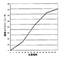
しかしながら、図10から分かるように、前フレームデータが0階調で目標階調が16のときにオーバードライブ階調として32が要求されるのに、前フレームデータが0階調で目標階調が15のときにオーバードライブ階調が15となり、目標階調の15と16の間で段差が残ることになる。この段差の残存は(特に、傾斜が大きいところでは)、図11に示すように、液晶画面においてスクロール時の尾引きとして目立つという欠点がある。
【0017】
次に、上記欠点を解消できる構成について図12乃至図17に基づいて説明していく。
【0018】
図12に示す構成の液晶パネル駆動装置において、フレームメモリ1からは8bit の前フレームデータが読み出される。入力データ(目標データ)も8bit である。前フレームデータの上位4bit 及び入力データの上位4bit がアドレスとしてルックアップテーブル(LUT)3に与えられる。このルックアップテーブル3は、各アドレスについて8bit データを持つが、その下位4bit は補完データを成すものである。この補完データは、前記段差(或いは傾斜)に対応したデータである。
【0019】
前フレームデータの下位4bit 及び入力データの下位4bit は演算回路4に入力される。また、ルックアップテーブル3の下位4bit (補完データ)も演算回路4に入力される。この演算回路4の一例を図13に示す。この図13に例示しているように、入力データの下位4bit が”1000”(8H)のとき、セレクタからの8bit 出力は”00010000”(10H)となり、前フレームデータの下位4bit が”0001”(1H)のとき、セレクタからの8bit 出力は”00000001”(01H)となる。そして、ルックアップテーブル3の出力に対して下位4bit が”0000”とされる処理がなされ、前述のセレクタ出力”00010000”(10H)が加算され、更に、前述のセレクタ出力”00000001”(01H)が減算されて、出力データ”11011111”(DFH)が得られることになる。
【0020】
上述した処理の概要は、図14に示すように、段差Sに応じて(上位ビットに応じて存在することになる下位4ビット補完データに応じて)目標階調に対するオーバードライブ階調を持ち上げる(傾斜をつける)ことに相当する。或る段差部分Snにおいて、入力データが”xxxx0000”〜”xxxx1111”の範囲ではルックアップテーブル3からの上位4bit は同じ(Sn0で示す階調)となるのであるが、内容をシンプルにして説明すると、要は、入力データが”xxxx1111”であるときには、階調を位置Sn0から段差Snの最上位置Sn15に持ち上げるように処理し、”xxxx0000”であるときには、階調を位置Sn0から持ち上げないで最下位置Sn0に維持するように処理し、その中間ではその中間に対応した持ち上げを行えばよいことになる。
【0021】
もっとも、8bit 入力データと8bit 前フレームデータをアドレスとしたときの8bit 出力データの中身は既知なのであるから、この既知の8bit 出力データに極力一致するように、入力データ下位4bit と前フレームデータ下位4bit とルックアップテーブル下位4bit を変数とした演算の中身を定めていけばよいことになる。この演算の中身としては、様々なものが考えられ得るものであるから、その演算内容を実現する演算回路についても様々なものが考えられるのであり、図12や図13に示した構成に限られないことは勿論である。
【0022】
また、上記の例による補正処理では、図15(前フレームデータが0階調の場合)にも示すように、段差Sに対する補正処理が直線的になるものであるが、これに限らず、図16に示すように、段差Sに対する補正処理が曲線的になるようにしてもよいものである。
【0023】
図17にはルックアップテーブル3の中身の一例を模式的に示している。この図において、△の領域にはデータは無く、演算で求めることになる。
【0024】
また、上記の例では、ルックアップテーブル3の8bit 中の上位4bit をLUTデータとし、下位4bit を補完データとして格納する例を示したが、これに限るものではない。例えば、ルックアップテーブル3として8bit メモリを使った場合、▲1▼LUTデータ6bit で補完データ2bit 、▲2▼LUTデータ5bit で補完データ3bit 、▲3▼LUTデータ3bit で補完データ5bit といった形態も採用し得る。また、ビット数を拡張したメモリを用いれば、▲4▼LUTデータ6bit で補完データ3bit (9bit メモリ)、▲5▼LUTデータ6bit で補完データ4bit (10bit メモリ)といった形態を採用することができる。
【0025】
補完データについては、これを4bit とする場合に、入力データ用に2bit 、前フレームデータ用に2bit といった割り振りで入力データと前フレームデータの両方を補完することができ、それぞれのビット数を増大させていくほど補正精度は高められる。ただし、このビット数はメモリ容量の削減効果との兼ね合いを考慮して定める。
【0026】
尚、オーバドライブとは、フレームメモリに記憶された前フレームデータによって示される階調よりも入力データによって示される階調(目標諧調)が大きい場合に、目標諧調よりも大きな諧調に相当するデータを出力し、このデータに基づいて過大電圧を液晶に印加する動作、あるいは、フレームメモリに記憶された前フレームデータによって示される階調よりも入力データによって示される階調(目標諧調)が小さい場合に、目標諧調よりも小さな諧調に相当するデータを出力し、このデータに基づいて過小電圧を液晶に印加する動作のいずれかの動作、もしくは両方の動作を、駆動動作の一部に含んだものを示す。したがって、ルックアップテーブルには、実験などによって求めたオーバドライブ用のデータが事前に記憶されている。
【0027】
上記実施形態は、周囲温度が一定値の場合を想定しているが、通常、表示装置の使用環境によって周囲温度は変化する。液晶は、周囲の温度によって、応答特性が変化するので、上記ルックアップテーブルを周囲温度別に複数設け、周囲温度に応じてルックアップテーブルを切り替えて用いる構成とすることもできる。また、ルックアップテーブルは1つでありながら、周囲温度に応じてルックアップテーブルの出力を、予め設定した温度補正用の計算式にしたがって補正して出力する構成とすることもできる。
【0028】
【発明の効果】
以上説明したように、この発明の液晶パネル駆動装置であれば、ルックアップテーブルのメモリ量を削減しつつ出力データ(オーバードライブデータ)の段差を極力少なくして映像表示品質を高めることができるという効果を奏する。
【図面の簡単な説明】
【図1】オーバードライブの概要を示した説明図である。
【図2】従来の液晶パネル駆動装置を示したブロック図である。
【図3】図5の従来装置のルックアップテーブルとして用いているメモリを示した説明図である。
【図4】図6の従来装置のルックアップテーブルとして用いているメモリを示した説明図である。
【図5】従来装置を示したブロック図である。
【図6】従来装置を示したブロック図である。
【図7】図5の従来装置のオーバードライブ階調を例示したグラフである。
【図8】図6の従来装置のオーバードライブ階調を例示したグラフである。
【図9】この発明の実施形態1の液晶パネル駆動装置を示した説明図である。
【図10】図9の構成によるオーバードライブ階調を例示したグラフである。
【図11】図10のオーバードライブ階調による画面表示状態を示した説明図である。
【図12】この発明の実施形態2の液晶パネル駆動装置を示した説明図である。
【図13】図12の演算回路の構成例を示した説明図である。
【図14】補正処理内容(直線的補正)を模式的に示した説明図である。
【図15】補正によるオーバードライブ階調を例示したグラフである。
【図16】他の補正処理内容(曲線的補正)を模式的に示した説明図である。
【図17】図12のルックアップテーブルの中身を例示した説明図である。
【符号の説明】
1 フレームメモリ
2 ルックアップテーブル
3 ルックアップテーブル
4 演算回路[0001]
[Industrial application fields]
The present invention relates to a liquid crystal panel driving apparatus that drives a liquid crystal panel at high speed by overdrive.
[0002]
[Prior art]
In order to increase the speed of the liquid crystal panel, as shown in FIG. 1, a method for improving the moving image display by performing overdrive driving in which a voltage higher than the normal voltage is applied has been proposed (Japanese Patent Laid-Open No. 2001-265298). No. IPC: G09G 3/36). Among these methods, as shown in FIG. 2, the
[0003]
[Problems to be solved by the invention]
However, in the above configuration that needs to have a look-up table, as shown in FIG. 3, when the previous frame data is 8 bits and the input data is 8 bits, the memory capacity increases (for
[0004]
SUMMARY OF THE INVENTION In view of the above circumstances, an object of the present invention is to provide a liquid crystal panel driving method or driving apparatus capable of reducing the step of output data as much as possible while reducing the memory capacity of a lookup table and suppressing the deterioration of display quality. And
[0005]
[Means for Solving the Problems]
In order to solve the above problems, a liquid crystal panel drive device according to the present invention is a part of previous frame data read from a frame memory in a liquid crystal panel drive device that performs overdrive using a frame memory and a lookup table. And a part of the input data are given to the look-up table as addresses, and overdrive data is generated based on the output data from the look-up table and the address unused portion of the input data. It is characterized by that.
[0006]
In the above configuration, for example, when the input data is “xxxx0001”, “0001” is combined with the output “yyyy” of the lookup table to become “yyy0001”, and the input data is, for example, “xxxx0011”. "," 0011 "is combined with the output" yyyy "of the look-up table and becomes" yyyy0011 ", so that the same gradation value is avoided, and the output level difference is minimized. Less. Since a part of the previous frame data and a part of the input data are input to the lookup table as addresses, the memory capacity can be reduced. As exemplified here, the address non-use portion is preferably composed of the lower bits of the input data.
[0007]
The liquid crystal panel drive device according to the present invention is a liquid crystal panel drive device that performs overdrive using a frame memory and a look-up table so that a part of the output data from the look-up table becomes complementary data. Is set, and a part of the previous frame data and a part of the input data are given to the lookup table as addresses, and the complementary data part in the output data from this lookup table and the address unused part of the input data The correction data is generated, and overdrive data is generated based on the correction data and the non-complementary data portion from the lookup table.
[0008]
The liquid crystal panel drive device according to the present invention is a liquid crystal panel drive device that performs overdrive using a frame memory and a look-up table so that a part of the output data from the look-up table becomes complementary data. Set, and a part of the previous frame data and a part of the input data are given to the look-up table as addresses, and the complementary data part in the output data from the look-up table, the address non-use part of the input data and the front Correction data is generated by an address non-use portion of the frame data, and overdrive data is generated based on the correction data and the non-complement data portion from the lookup table. To do.
[0009]
With these configurations, the data obtained when the part of the previous frame data and the part of the input data are given to the look-up table as addresses include supplementary data. By having data corresponding to the inclination, correction data can be generated by the address non-use portion of the input data, and further by the address non-use portion of the previous frame data. It is possible to appropriately correct the complementary data portion to fill the step.
[0010]
The complementary data may be composed of lower bits of output data of the lookup table.
[0011]
DETAILED DESCRIPTION OF THE INVENTION
Hereinafter, an embodiment of a driving method or a driving apparatus according to the present invention will be described with reference to FIGS.
[0012]
In the liquid crystal panel driving apparatus having the configuration shown in FIG. 9, the
[0013]
This input data is output from the
[0014]
In the example shown in the figure, when the upper 4 bits “1100” of the input data “11001000” (C8H) and the upper 4 bits “0011” of the previous frame data “00110001” (31H) are given to the lookup table 2 as addresses, the output Becomes “1101”, and the lower 4 bits “1000” of the input data are added to this, and 8 bit data “11011000” (D8H) is output.
[0015]
As a result, as shown in FIG. 10 (in the case where the previous frame data is 0 gradation), the output step is reduced with respect to the gradation step generated when the conventional small-capacity memory is used as a lookup table (see FIG. 8). It can be reduced as much as possible. That is, when the input data is “xxxx0001”, “0001” is combined with the output “yyyy” of the lookup table to become “yyyy0001”, and when the input data is “xxxx0011”, for example, Since “0011” is combined with the output “yyyy” of the uptable to become “yyyy0011”, the same gradation value is avoided.
[0016]
However, as can be seen from FIG. 10, when the previous frame data is 0 gradation and the target gradation is 16, an overdrive gradation of 32 is required, but the previous frame data is 0 gradation and the target gradation is In the case of 15, the overdrive gradation becomes 15, and a step remains between the
[0017]
Next, a configuration that can eliminate the above-described drawbacks will be described with reference to FIGS.
[0018]
In the liquid crystal panel driving apparatus having the configuration shown in FIG. 12, 8-bit previous frame data is read from the
[0019]
The lower 4 bits of the previous frame data and the lower 4 bits of the input data are input to the
[0020]
As shown in FIG. 14, the outline of the above-described processing raises the overdrive gradation with respect to the target gradation according to the step S (according to the lower 4-bit complementary data that will exist according to the upper bit) ( Equivalent to adding a slope). In a certain step portion Sn, the upper 4 bits from the lookup table 3 are the same (gradation indicated by Sn0) when the input data is in the range of “xxxx0000” to “xxxx1111”. In short, when the input data is “xxxx 1111”, the gradation is processed to be raised from the position Sn0 to the highest position Sn15 of the step Sn, and when it is “xxxx0000”, the gradation is not raised from the position Sn0. Processing is performed so as to maintain the lower position Sn0, and in the middle, lifting corresponding to the middle may be performed.
[0021]
However, since the contents of 8bit output data when 8bit input data and 8bit previous frame data are used as addresses are known, lower 4bit of input data and lower 4bit of previous frame data are matched as much as possible to this known 8bit output data. And the contents of the operation with the lower 4 bits of the lookup table as variables should be determined. Since various contents can be considered as the contents of this calculation, various kinds of arithmetic circuits for realizing the contents of the calculation can be considered, and are limited to the configurations shown in FIG. 12 and FIG. Of course not.
[0022]
Further, in the correction process according to the above example, as shown in FIG. 15 (when the previous frame data is 0 gradation), the correction process for the step S is linear, but the present invention is not limited to this. As shown in FIG. 16, the correction process for the step S may be curved.
[0023]
FIG. 17 schematically shows an example of the contents of the lookup table 3. In this figure, there is no data in the region of Δ, and it is obtained by calculation.
[0024]
In the above example, the upper 4 bits of the 8 bits of the lookup table 3 are stored as LUT data and the lower 4 bits are stored as complementary data. However, the present invention is not limited to this. For example, when an 8-bit memory is used as the look-up table 3, (1) LUT data 6 bits and complementary data 2 bits, (2) LUT data 5 bits, complementary data 3 bits, and (3) LUT data 3 bits and complementary data 5 bits are also used. Can do. If a memory with an expanded number of bits is used, it is possible to adopt forms such as (4) 6 bits of LUT data and 3 bits of complementary data (9-bit memory), and (5) 6 bits of LUT data and 4 bits of complementary data (10-bit memory).
[0025]
For complementary data, if this is set to 4 bits, both input data and previous frame data can be complemented by allocating 2 bits for input data and 2 bits for previous frame data, increasing the number of each bit. The correction accuracy increases as the time increases. However, the number of bits is determined in consideration of the effect of reducing the memory capacity.
[0026]
Note that overdrive refers to data corresponding to a tone larger than the target tone when the tone (target tone) indicated by the input data is larger than the tone indicated by the previous frame data stored in the frame memory. Output and applying an excessive voltage to the liquid crystal based on this data, or when the gradation (target gradation) indicated by the input data is smaller than the gradation indicated by the previous frame data stored in the frame memory , Output data corresponding to a gradation smaller than the target gradation, and apply either an operation of applying an undervoltage to the liquid crystal based on this data, or both operations included as part of the drive operation Show. Therefore, the overdrive data obtained by experiments or the like is stored in advance in the lookup table.
[0027]
In the above embodiment, it is assumed that the ambient temperature is a constant value, but the ambient temperature usually varies depending on the use environment of the display device. Since the response characteristics of the liquid crystal change depending on the ambient temperature, a plurality of lookup tables may be provided for each ambient temperature, and the lookup table may be used by switching according to the ambient temperature. Further, although there is only one look-up table, the output of the look-up table may be corrected according to a preset temperature correction formula and output according to the ambient temperature.
[0028]
【The invention's effect】
As described above, with the liquid crystal panel driving device of the present invention, it is possible to improve the video display quality by reducing the step of the output data (overdrive data) as much as possible while reducing the memory amount of the lookup table. There is an effect.
[Brief description of the drawings]
FIG. 1 is an explanatory diagram showing an outline of overdrive.
FIG. 2 is a block diagram showing a conventional liquid crystal panel driving device.
3 is an explanatory diagram showing a memory used as a lookup table of the conventional apparatus of FIG. 5; FIG.
4 is an explanatory diagram showing a memory used as a lookup table of the conventional apparatus of FIG. 6; FIG.
FIG. 5 is a block diagram showing a conventional apparatus.
FIG. 6 is a block diagram showing a conventional apparatus.
7 is a graph illustrating the overdrive gradation of the conventional device of FIG.
FIG. 8 is a graph illustrating overdrive gray levels of the conventional device of FIG. 6;
FIG. 9 is an explanatory diagram showing a liquid crystal panel driving device according to
10 is a graph illustrating overdrive gray levels according to the configuration of FIG. 9;
11 is an explanatory diagram showing a screen display state by overdrive gradation of FIG.
FIG. 12 is an explanatory view showing a liquid crystal panel driving device of Embodiment 2 of the present invention.
13 is an explanatory diagram showing a configuration example of an arithmetic circuit in FIG. 12. FIG.
FIG. 14 is an explanatory diagram schematically showing the content of correction processing (linear correction).
FIG. 15 is a graph illustrating an overdrive gradation by correction.
FIG. 16 is an explanatory view schematically showing other correction processing contents (curve correction).
FIG. 17 is an explanatory diagram illustrating the contents of the lookup table of FIG. 12;
[Explanation of symbols]
1 Frame memory 2 Look-up table 3 Look-up table 4 Arithmetic circuit
Claims (1)
Priority Applications (1)
| Application Number | Priority Date | Filing Date | Title |
|---|---|---|---|
| JP2002242185A JP4186552B2 (en) | 2002-08-22 | 2002-08-22 | LCD panel drive |
Applications Claiming Priority (1)
| Application Number | Priority Date | Filing Date | Title |
|---|---|---|---|
| JP2002242185A JP4186552B2 (en) | 2002-08-22 | 2002-08-22 | LCD panel drive |
Publications (2)
| Publication Number | Publication Date |
|---|---|
| JP2004078129A JP2004078129A (en) | 2004-03-11 |
| JP4186552B2 true JP4186552B2 (en) | 2008-11-26 |
Family
ID=32024454
Family Applications (1)
| Application Number | Title | Priority Date | Filing Date |
|---|---|---|---|
| JP2002242185A Expired - Fee Related JP4186552B2 (en) | 2002-08-22 | 2002-08-22 | LCD panel drive |
Country Status (1)
| Country | Link |
|---|---|
| JP (1) | JP4186552B2 (en) |
Families Citing this family (14)
| Publication number | Priority date | Publication date | Assignee | Title |
|---|---|---|---|---|
| JP4807938B2 (en) | 2004-05-14 | 2011-11-02 | ルネサスエレクトロニクス株式会社 | Controller driver and display device |
| JP4902116B2 (en) * | 2004-12-27 | 2012-03-21 | 株式会社 日立ディスプレイズ | Liquid crystal display |
| JP2006227235A (en) * | 2005-02-17 | 2006-08-31 | Seiko Epson Corp | Liquid crystal device, image display device using the same, and driving method of liquid crystal device |
| JP4574676B2 (en) | 2005-03-31 | 2010-11-04 | シャープ株式会社 | Driving method of liquid crystal display device |
| US8264441B2 (en) | 2005-03-31 | 2012-09-11 | Sharp Kabushiki Kaisha | Method for driving liquid crystal display apparatus |
| US8384639B2 (en) | 2006-02-07 | 2013-02-26 | Sharp Kabushiki Kaisha | Liquid crystal display device and method for emphasizing temporal signal change on a video signal based on at least a polarity for the video signal |
| JP2007233120A (en) * | 2006-03-02 | 2007-09-13 | Matsushita Electric Ind Co Ltd | Liquid crystal display |
| JP2008096875A (en) * | 2006-10-16 | 2008-04-24 | Infovision Optoelectronics Holdings Ltd | Driving circuit for active matrix type liquid crystal display device and active matrix type liquid crystal display device |
| KR101046583B1 (en) * | 2006-11-27 | 2011-07-06 | 삼성전자주식회사 | Image processing apparatus and control method |
| KR101293560B1 (en) | 2007-01-23 | 2013-08-06 | 삼성디스플레이 주식회사 | Display device and driving method thereof |
| KR100858479B1 (en) * | 2007-05-18 | 2008-09-12 | 시트로닉스 테크놀로지 코퍼레이션 | Driving method to improve response time of twisted nematic and super twisted nematic liquid crystal display without increasing graphic RAM |
| JP5010391B2 (en) | 2007-08-17 | 2012-08-29 | ザインエレクトロニクス株式会社 | Image signal processing device |
| KR20100025095A (en) * | 2008-08-27 | 2010-03-09 | 삼성전자주식회사 | Method for compensating image data, compensating apparatus for performing the method and display device having the compensating apparatus |
| KR101893949B1 (en) | 2017-12-07 | 2018-10-04 | 삼익전자공업 주식회사 | LED Individual Correction Method Based On The Operating Computer Of The LED Signboard |
-
2002
- 2002-08-22 JP JP2002242185A patent/JP4186552B2/en not_active Expired - Fee Related
Also Published As
| Publication number | Publication date |
|---|---|
| JP2004078129A (en) | 2004-03-11 |
Similar Documents
| Publication | Publication Date | Title |
|---|---|---|
| JP4186552B2 (en) | LCD panel drive | |
| KR100683997B1 (en) | LCD Panel Driver | |
| US6853384B2 (en) | Liquid crystal display device and driving method thereof | |
| JP3763397B2 (en) | Image processing apparatus, image display apparatus, personal computer, and image processing method | |
| KR100859514B1 (en) | Liquid crystal display and its driving device | |
| JP4912661B2 (en) | Display device and driving device thereof | |
| JP2006506664A (en) | Liquid crystal display device and driving method thereof | |
| JP4296381B2 (en) | Method and apparatus for driving liquid crystal display device | |
| JP2006506665A (en) | Liquid crystal display device and driving method thereof | |
| CN113223467A (en) | Display device and method of driving the same | |
| US20090091588A1 (en) | Liquid crystal driving method and circuit | |
| CN119496883A (en) | Image processing circuit and method | |
| JP4409843B2 (en) | Control circuit for liquid crystal display device performing drive compensation | |
| US20080297497A1 (en) | Control circuit and method of liquid crystal display panel | |
| JP2004109796A (en) | Liquid crystal panel driving device | |
| KR100570614B1 (en) | Gradient Representation Method of High Load Screen and Plasma Display Panel Driving Device Using the Method | |
| US7098874B2 (en) | Method and apparatus of driving plasma display panel | |
| JP4134550B2 (en) | Image display device | |
| JP2005037749A (en) | Liquid crystal drive device | |
| JP2009003180A (en) | Display method and display device | |
| JP2004343560A (en) | Image processing method, image processor, and liquid crystal display device using them | |
| JP3944204B2 (en) | Image processing apparatus and image display apparatus having the same | |
| JP2008111925A (en) | Liquid crystal display apparatus | |
| JP4369837B2 (en) | Image processing apparatus and image display apparatus having the same | |
| JP2005043725A (en) | Display device and medium gradation display method |
Legal Events
| Date | Code | Title | Description |
|---|---|---|---|
| A621 | Written request for application examination |
Free format text: JAPANESE INTERMEDIATE CODE: A621 Effective date: 20050712 |
|
| RD01 | Notification of change of attorney |
Free format text: JAPANESE INTERMEDIATE CODE: A7421 Effective date: 20051227 |
|
| A711 | Notification of change in applicant |
Free format text: JAPANESE INTERMEDIATE CODE: A711 Effective date: 20070228 |
|
| A131 | Notification of reasons for refusal |
Free format text: JAPANESE INTERMEDIATE CODE: A131 Effective date: 20071225 |
|
| A521 | Written amendment |
Free format text: JAPANESE INTERMEDIATE CODE: A523 Effective date: 20080222 |
|
| A131 | Notification of reasons for refusal |
Free format text: JAPANESE INTERMEDIATE CODE: A131 Effective date: 20080513 |
|
| A521 | Written amendment |
Free format text: JAPANESE INTERMEDIATE CODE: A523 Effective date: 20080711 |
|
| TRDD | Decision of grant or rejection written | ||
| A01 | Written decision to grant a patent or to grant a registration (utility model) |
Free format text: JAPANESE INTERMEDIATE CODE: A01 Effective date: 20080819 |
|
| A01 | Written decision to grant a patent or to grant a registration (utility model) |
Free format text: JAPANESE INTERMEDIATE CODE: A01 |
|
| A61 | First payment of annual fees (during grant procedure) |
Free format text: JAPANESE INTERMEDIATE CODE: A61 Effective date: 20080901 |
|
| R150 | Certificate of patent or registration of utility model |
Free format text: JAPANESE INTERMEDIATE CODE: R150 |
|
| FPAY | Renewal fee payment (event date is renewal date of database) |
Free format text: PAYMENT UNTIL: 20110919 Year of fee payment: 3 |
|
| FPAY | Renewal fee payment (event date is renewal date of database) |
Free format text: PAYMENT UNTIL: 20120919 Year of fee payment: 4 |
|
| FPAY | Renewal fee payment (event date is renewal date of database) |
Free format text: PAYMENT UNTIL: 20130919 Year of fee payment: 5 |
|
| S531 | Written request for registration of change of domicile |
Free format text: JAPANESE INTERMEDIATE CODE: R313531 |
|
| R350 | Written notification of registration of transfer |
Free format text: JAPANESE INTERMEDIATE CODE: R350 |
|
| LAPS | Cancellation because of no payment of annual fees |