JP4173555B2 - Flash memory VDS compensation technology to eliminate programming variability - Google Patents
Flash memory VDS compensation technology to eliminate programming variability Download PDFInfo
- Publication number
- JP4173555B2 JP4173555B2 JP54160898A JP54160898A JP4173555B2 JP 4173555 B2 JP4173555 B2 JP 4173555B2 JP 54160898 A JP54160898 A JP 54160898A JP 54160898 A JP54160898 A JP 54160898A JP 4173555 B2 JP4173555 B2 JP 4173555B2
- Authority
- JP
- Japan
- Prior art keywords
- voltage
- source
- memory cell
- bit line
- source line
- Prior art date
- Legal status (The legal status is an assumption and is not a legal conclusion. Google has not performed a legal analysis and makes no representation as to the accuracy of the status listed.)
- Expired - Fee Related
Links
Images


Classifications
-
- G—PHYSICS
- G11—INFORMATION STORAGE
- G11C—STATIC STORES
- G11C11/00—Digital stores characterised by the use of particular electric or magnetic storage elements; Storage elements therefor
- G11C11/21—Digital stores characterised by the use of particular electric or magnetic storage elements; Storage elements therefor using electric elements
- G11C11/34—Digital stores characterised by the use of particular electric or magnetic storage elements; Storage elements therefor using electric elements using semiconductor devices
-
- G—PHYSICS
- G11—INFORMATION STORAGE
- G11C—STATIC STORES
- G11C16/00—Erasable programmable read-only memories
- G11C16/02—Erasable programmable read-only memories electrically programmable
- G11C16/06—Auxiliary circuits, e.g. for writing into memory
- G11C16/10—Programming or data input circuits
-
- G—PHYSICS
- G11—INFORMATION STORAGE
- G11C—STATIC STORES
- G11C16/00—Erasable programmable read-only memories
- G11C16/02—Erasable programmable read-only memories electrically programmable
- G11C16/06—Auxiliary circuits, e.g. for writing into memory
- G11C16/30—Power supply circuits
Description
発明の分野
本発明はメモリ・セルをプログラムすることに関する。より詳細には、本発明は、メモリ装置内のフラッシュ・メモリ・セルのプログラム時にソース電圧とドレイン電圧を補償する方法と回路に関する。
背景
電気的プログラム可能読取専用メモリ(「EPROM」)、電気的消去可能プログラム可能読取専用メモリ(「EEPROM」)、フラッシュEEPROMなどの不揮発性メモリ装置は、不揮発性メモリ・セルのアレイと、そのアレイにアクセスするためのサポート回路を含む。典型的には、不揮発性メモリ・セルは電界効果トランジスタと同様の挙動を示し、データのメモリ・セルへの読み取りおよび書き込みを制御する選択ゲートまたは制御ゲート、およびメモリ・セルが記憶したデータに対応する電荷をトラップする浮動ゲートを含む。
不揮発性半導体メモリの魅力的な機能はアナログ・データを記憶できる能力である。すなわち、複数ビットのデータを単一のメモリ・セルに記憶できる。メモリ・セルの浮動ゲートに電荷が加えられると、メモリ・セルのしきい値電圧Vtが増大し、メモリ・セルのドレイン電流ID(「セル電流」)が減少する。メモリ・セルしきい値電圧Vtは、IDが次式に比例するような形でメモリ・セルのドレイン電流IDと関係する。
Gm×(VG−Vt) VD>VG−Vtの場合
(式1)
この式でGmはメモリ・セルの相互コンダクタンス、VGはメモリ・セルのゲート電圧、VDはメモリ・セルのドレイン電圧、Vtはメモリ・セルのしきい値電圧である。
複数ビットのデータを記憶するメモリ・セルでは、可能な各ビット・パターンはそれぞれ1つの状態を表す。実際に、セルはベースSデータを記憶している。Sはセルが記憶できる状態の数である。ビット・パターンは、1つまたは複数のセルの状態データを復号化した結果得られる。たとえば、2ビットのデータを記憶しているメモリ・セルでは、00、01、10、11の4種類のビット・パターンがある。これらの各ビット・パターンは、それぞれ1つの状態で表される。特定のビット・パターンによって表される特定の状態は、使用される符号化のタイプによって異なる(たとえばグレー・コーディング、バイナリなど)。符号化のタイプは一般的に、プログラミングの方法に影響を与えない。
状態は種々の方法で定義できる。しきい値電圧Vtの範囲で定義することもできるし、ドレイン電流IDの範囲、または電荷の範囲で定義することもできる。
第1図は、フラッシュ・メモリ・アレイ100の周知の部分を示している。ワード線138および140とビット線146および148の交点で形成されたフラッシュ・メモリ・セル112、114、116、118を含む。各フラッシュ・メモリ・セルは選択ゲートと浮動ゲートを含む。たとえば、フラッシュ・メモリ・セル112は制御ゲート144と浮動ゲート142を含む。フラッシュ・メモリ・セル112と114はワード線138に結合された制御ゲートを有し、フラッシュ・メモリ・セル116と118はワード線140に結合された制御ゲートを有する。フラッシュ・メモリ・セル112と116は、ビット線146に結合された1個の端子または電極と、共通ソース線150に結合された別の端子あるいは電極を有する。共通ソース線はソース電圧VPSに結合されている。同様に、フラッシュ・メモリ・セル114と118は、ビット線148に結合された1つの端子あるいは電極と、共通ソース線150に結合された別の端子あるいは電極を有する。
ワード線138と140は、各ワード線が、フラッシュ・メモリ・セル112、114、116、118にデータを読み取り、消去、プログラムするために必要な電圧を各ワード線に提供するX復号器回路に結合されているため、X線あるいは行線とも呼ばれる。同様に、ビット線146と148は、各ビット線が、フラッシュ・メモリ・セル112、114、116、118にデータを読み取り、消去、プログラムするために必要な電圧VPPを各ビット線に提供するY復号器回路と電圧生成回路に結合されているため、Y線あるいは列線とも呼ばれる。
ビット線、ワード線、共通ソース線は、これらでアレイ100の中でメモリ・セルをプログラムしたり、消去したり、読み取りするために必要な電圧をメモリ・セルに加える手段を構成している。メモリ・セル112、114、116、118は、ワード線138と140に約ゼロ・ボルトを加え、ビット線146と148を浮動させ、VPSを共通ソース線150に約12ボルトに設定することによってファウラー・ノルドハイム・トンネル効果を使用して消去できる。この構成では、メモリ・セルのアレイ全体が一度に消去できる。代替方法としては、メモリ・セルのアレイ全体を負のゲート消去を使用しても消去できる。すなわち、VPSを約5〜6ボルトに設定し、ワード線146と148に約−8〜−10ボルトを加えることによっても消去できる。メモリ・セル112、114、116、118はワード線138と140に約1〜7ボルトを加え、ビット線146と148上のVPPに約1ボルトを加え、共通ソース線150を接地させることによって読み取ることができる。
メモリ・セル112、114、116、118はまた、ビット線146または148にVPSより約4〜7ボルト高いVPPを加え、保存されている電荷の量とプログラムされているメモリ・セルのしきい値電圧を十分に変更できる電圧をワード線138または140に加えることによって、ホット電子注入によりプログラムできる。典型的には、メモリ・セルの他の行を選択せずに、ある行の1つまたは複数のフラッシュ・メモリ・セルを1度にプログラムできる。
一般的に、フラッシュ・メモリ・セルのプログラミング時間は、プログラミング中にメモリ・セルに印加されるドレイン・プログラミング電圧とソース・プログラミング電圧の差に反比例して変化する。第2図は、プログラミング中の、ソース・プログラミング電圧VSが約ゼロ・ボルトの時にメモリ・セルに加えられるプログラミング・ドレイン電圧VDに応じた、プログラミング時間に対するフラッシュ・メモリ・セルのしきい値電圧Vtの関係を示している。
第2図で、曲線223は、ドレイン・プログラミング電圧VDが約6ボルトで、ソース・プログラミング電圧VSが約ゼロ・ボルトの時における、プログラミング時間のしきい値電圧とフラッシュ・メモリ・セルの関係を示している。曲線224は、プログラミング・ドレイン電圧が約5ボルトでソース・プログラミング電圧VSが約ゼロ・ボルトの時における、フラッシュ・メモリ・セルのしきい値電圧とプログラミング時間の関係を示している。第2図に示すように、プログラミング・ドレイン電圧とソース・プログラミング電圧の差が比較的大きい場合、フラッシュ・メモリ・セルが同じしきい値電圧に達するまでのプログラミング時間はそれに従って短くなる。
第1図は、各ビット線146と148とソース線150が、ビット線を作成するために使用される材料(種々の金属、ドープされた)シリコン、ポリシリコンなど)に固有の電気的性質、物理的性質によりシステム的な抵抗を有することをも示している。たとえば、ビット線146は抵抗120と122を有し、ビット線148は抵抗124と126、共通ソース線150は抵抗128、130、132、134、136を有する。ビット線抵抗とソース線抵抗の値は、メモリ・アレイ100におけるフラッシュ・メモリ・セルの位置の関数であり、したがってシステムによる。物理的な線の抵抗は線の幾何形状によって異なり、一般的には次式で表される。
R=p×(L/A)
(式2)
この式でRは線の抵抗、pは線が作られた材料の抵抗率、Lは線の長さ、Aは線の断面積である。一般に、式2で示すように線の長さが長くなるにつれて、線の抵抗も大きくなる。したがって、フラッシュ・メモリ端子が電圧源(VSPあるいはVPPなど)から離れれば離れるほど抵抗は大きくなり、電圧源から供給される電圧からの逸脱が大きくなる。
たとえば、フラッシュ・メモリ・セル116のプログラミング中にVPSがゼロ・ボルトに設定されている場合、ゼロ・ボルトだったのが各抵抗136、134、130を通じて大きくなる。したがって、メモリ・セル116のソースにおいてソース・プログラミング電圧VSとして実際に表れる電圧は、ゼロ・ボルトより大きい電圧になる。同様に、プログラミング電圧VPPはビット線146の一番上では6ボルトで始まるが、120と122の各抵抗を通じて電圧低下を受け、ドレイン・プログラミング電圧は6ボルト未満になってしまう。したがって、プログラミング電圧差VPP−VPSに比べると、実際のプログラミング電圧差VD−VSは大幅に減少し、メモリ・セル116を所定の状態にプログラムするのに必要な時間が増加する。したがって、一般にプログラム電圧源VPPおよびVSSに近いフラッシュ・メモリ・セルをプログラムするより、プログラム電圧源VPPおよびVSSから遠いフラッシュ・メモリ・セルをプログラムする方が多くの時間が必要になる。
ビット線抵抗とソース線抵抗はまた、所与のプログラミング時間で、同じ状態にプログラムされるはずのメモリ・セルを異なる状態にプログラムさせることがある。たとえば、電圧源VPPおよびVPSに近い位置にあるメモリ・セル118のVD電圧とVS電圧はVPPとVPSに近く、所与のプログラミング時間内に特定の状態にプログラムされる。逆に、電圧源VPPおよびVPSから遠い位置にあるメモリセル116のVD電圧とVS電圧はVPPとVPSからかなり遠いので、メモリ・セル116は同じプログラミング時間内に、異なる状態にプログラムされる。したがって、フラッシュ・メモリ・セルがフラッシュ・メモリ・アレイ100中で占める位置によって、ある程度のプログラミングの変動性がある。
システムのソース線抵抗は、ある時間に同時にプログラムされるフラッシュ・メモリ・セルの数に対してソース・プログラミング電圧VSを変化させる。所与のフラッシュ・メモリ・ブロック内にある各フラッシュ・メモリ・セルのソース端子は共通ソース線150に接続されているので、共通ソース線150中を流れる電流は、一度にプログラムされるフラッシュ・メモリ・セルの数に応じて変化する。電流が共通ソース線150内で変化するため、フラッシュ・メモリ・セルの各ソースに結合された電圧も変化する。一般に、一度にプログラムされるセルの数が増えるとVSも増大する。したがって、各フラッシュ・メモリ・セルに結合されたソース・プログラミング電圧VSは、フラッシュ・メモリ装置に供給されるデータ・パターンにも依存する。
ビット線抵抗やソース線抵抗の負の影響を打ち消すために、いくつかの技術が開発されている。ある技術では、フラッシュ・メモリ・アレイ内で抵抗が低い金属線をソース・ストラップとして使用することにより、ソース線抵抗を減少させている。しかしこの技術を使用しても、選択されたメモリ・セルがソース・ストラップに対してどのような位置にあるかにより、フラッシュ・メモリ・セルに加えられるソース電圧が異なる結果になる。
米国特許第5420370に開示された別の技術では、装置ごとにビット線の一番上に加えられるドレイン・プログラミング電圧源を調節し、メモリ・セルのチャネル長さの中で、装置間のばらつきによるフラッシュ・メモリ・セルのプログラミング能力の変化を補償する。この技術は、ビット線抵抗やソース線抵抗を補償するためにプログラミング電圧源を変化させることはない。
さらに別の技術では、あるドレイン・プログラミング電圧をフラッシュ・メモリ・セル・ブロックの上半分に供給し、別のドレイン・プログラミング電圧をフラッシュ・メモリ・セル・ブロックの下半分に供給することによってビット線抵抗を補償する。この技術はソース線抵抗およびデータ・パターンの依存性を補償しない。
発明の概要
本発明では不揮発性メモリ装置と、プログラミング電圧を設定する方法を記述する。一態様では、不揮発性メモリ装置はビット線と、ソース線と、不揮発性メモリ・セルとを含む。不揮発性メモリ・セルは、ビット線に結合されたドレイン、ソース線に結合されたソース、制御ゲートおよび浮動ゲートを有する。不揮発性メモリ・セルとを含む。また、不揮発性メモリ装置は、ソース線に結合され、不揮発性メモリ・セルをプログラミングする時にソース線電圧を生成するソース電圧生成回路を含む。そのソース電圧生成回路は、メモリ・アレイ内における不揮発性メモリ・セルの位置に基づいてソース線電圧を変化させる。さらに、不揮発性メモリ装置は、ビット線に結合され、不揮発性メモリ・セルをプログラミングする時にビット線電圧を生成するドレイン電圧生成回路をも含む。ドレイン電圧生成回路は、メモリ・アレイ内における不揮発性メモリ・セルの位置に基づいて、ビット線電圧を変化させる。
本発明の他の特徴や利点は、添付の図面と以下の詳細な説明から明らかになるであろう。
【図面の簡単な説明】
本発明の特徴と利点は添付の図面に限定的ではなく例として示される。図中、同じ参照番号は同様の要素を指す。
第1図は、ビット線抵抗とソース線抵抗を含む従来技術のフラッシュ・メモリアレイである。
第2図は、ソース・プログラミング電圧を固定し、ドレイン・プログラミング電圧を変化させた場合の、フラッシュ・メモリ・セルのしきい値電圧とプログラミングの関係を示す電圧時間図である。
第3図は、ドレイン電圧生成回路と、ソース電圧生成回路を含むフラッシュ・メモリ装置の構成図である。
第4図は、メモリ・ブロックにセグメント化されたフラッシュ・メモリの一実施例を示す構成図である。
第5図は、アドレス復号器、データ・パターン・モニタ、ドレイン電圧生成回路、ソース電圧生成回路、フラッシュ・メモリ・セル、ビット線抵抗、ソース線抵抗を含む、第3図のフラッシュ・メモリ装置の一実施形態を示す構成図である。
第6図は、第3図のドレイン電圧生成器の一実施形態を示す構成図である。
第7図は、第3図のソース電圧生成器の一実施形態を示す構成図である。
第8図は、テスト・システムに結合された第3図のフラッシュ・メモリ装置を示す構成図である。
第9図は、第3図のドレイン電圧生成器および/またはソース電圧生成器を特徴付け、調整する設定の一実施形態を示すフロー・チャートである。
発明の詳細な説明
フラッシュ・メモリ・セルのソース・プログラミング電圧とドレイン・プログラミング電圧を設定する方法と装置を説明する。以下に説明する実施形態は、ビット線電圧またはソース線電圧を調整して、フラッシュ・メモリ・アレイに存在するシステムのビット線抵抗およびソース線抵抗を補償し、それによってメモリ・アレイ全体を通して各フラッシュ・メモリ・セルごとにドレイン・プログラミング電圧とソース・プログラミング電圧の差を実質的に均一に維持する実施形態である。ビット線抵抗とソース線抵抗を補償する目的は、フラッシュ・メモリ・セルのプログラミング速度を増大させ、異なる位置にあるメモリ・セルが異なる値にプログラムされる原因となるプログラミングの変動性を低減し、一度に複数のフラッシュ・メモリ・セルをプログラミングすることによって生じるプログラムの変動性を低減する助けとなることである。
以下に詳しく説明するように、本発明の一実施形態は、不揮発性メモリ・アレイ、制御回路、ソース電圧生成器、およびドレイン電圧生成器を有する不揮発性メモリ装置を含む。メモリ・アレイは第1図に示したようにアレイされ、ドレイン電圧生成器とソース電圧生成器の間にビット線抵抗とソース線抵抗を有するフラッシュ・メモリ・セルを含む。制御回路はアレイ内のプログラムされるフラッシュ・メモリ・セルのアドレスを受け取る。制御回路はアドレスを復号し、フラッシュ・メモリ・セルのアドレスをソース電圧生成回路とドレイン電圧生成器に示す。ソース電圧生成器は選択されたフラッシュ・メモリ・セルのアドレスに基づいて、ソース電圧生成器と選択されたフラッシュ・メモリ・セルのソースの間のソース線抵抗を補償するソース線電圧を生成する。同様に、ドレイン電圧生成器は選択されたフラッシュ・メモリ・セルのアドレスに基づいて、ドレイン電圧生成器と選択されたフラッシュ・メモリ・セルの間のビット線抵抗を補償するビット線電圧を生成する。したがって、フラッシュ・メモリ・アレイにおけるメモリ・セルの位置にかかわらず、選択されたメモリ・セルには実質的に一定のドレイン−ソース(VDS)プログラミング電圧差が加えられ、その結果、実質的にプログラミング速度は均一になり、プログラミングの変動性は低減する。
第3図は、本発明の実施形態を実施することのできる不揮発性メモリ装置300を示す。以下に説明する実施形態は、情報の複数の状態を記憶できるメモリ・セルを含むDRAMアレイを含んだ不揮発性メモリ・アレイでも実施できる。
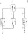
メモリ装置300はコマンド・インタフェース302、制御回路304、ドレイン電圧生成器308、ソース電圧生成器312、Y復号器316、X復号器318、Yゲート&センス増幅器320、およびメモリ・アレイ322を含む。一実施形態では、フラッシュ・メモリ装置300のすべての回路は単一の基板上にある。
メモリ・アレイ322は、第1図に示すように行と列に配置された不揮発性メモリ・セルを含む。不揮発性メモリ・セルはそれぞれのアドレスにデータを記憶する。不揮発性メモリ・セルのしきい値電圧はプログラミング中に変更することができ、したがってアナログ電圧レベルの記憶が可能である。一実施形態では、メモリアレイ322内の各メモリ・セルは、一度に1ビットのデータを記憶する。別の実施形態では、メモリ・アレイ322内の各メモリ・セルは一度に複数ビットのデータを記憶する。メモリ・アレイ322内のメモリ・セルは一般に上記のようにプログラムされ、消去され、読み取られるが、選択されたメモリ・セルのソース端子とドレイン端子に加えられるプログラミング電圧は以下に説明するように生成される。
メモリ・アレイ322は1つのメモリ・アレイを有する場合もあり、メモリ・セルのブロックを有する場合もある。メモリ・セルの各ブロックはそれぞれ独立にアドレスされる。たとえば、1つのアドレス信号線が、選択されたフラッシュ・メモリ・セルが入っているメモリ・ブロックを示し、アドレス信号線の残り部分が、その選択されたメモリ・ブロック内の選択されたメモリ・セルの位置を示すことができる。
メモリ装置300の一実施形態では、制御エンジン304はメモリ・アレイ322内の選択された1つまたは複数のメモリ・セルのプログラミングを制御する。一実施形態では、制御エンジン304はマイクロコードが制御するプロセッサを含む。別の実施形態では、制御エンジン304は、メモリ・アレイ322内のメモリ・セルをプログラムするための種々の機能を実施する状態マシンあるいは論理回路である。
制御エンジン304は、X復号器318、Y復号器316、Yゲート&センス増幅器320、ドレイン電圧生成器308、およびソース電圧生成器312の制御によってメモリ・アレイ322を管理する。制御回路304は、外部回路から加えられてバス326をアドレスし、バス336を介してY復号器316およびX復号器318に供給されるアドレスをラッチするための、アドレス・ラッチを含むこともできる。Yゲート&センス増幅器320は、メモリ・アレイ322から読み取られたデータ、または、メモリ・アレイ322にプログラムされるデータをバッファする。
読み取り、消去、プログラムのためのユーザ・コマンドはコマンド・インタフェース302を介して制御回路304に送られる。外部ユーザは、出力可能化OEB、チップ選択CEB、書き込み可能化WEBを含む制御信号を介してコマンド・インタフェース302にコマンドを発行する。他の制御信号を使用することもできる。コマンド・インタフェース302は電源電圧VCC、接地電圧VSS、プログラミング/消去電圧VPPを受け取る。VCCとVSSは、フラッシュ・メモリ装置300内の各回路に結合される。一実施形態では、VCCは約3〜6ボルトである。VPPはフラッシュ・メモリ装置300の内部で生成することもできるし、外部から供給することもできる。メモリ・アレイ322内の選択されたフラッシュ・メモリ・セルをプログラミングする間、VPPの範囲は約5〜13ボルトの間である。
フラッシュ・メモリ装置300は、フラッシュ・メモリ装置300用に制御信号、アドレス信号および/またはデータ信号を生成する、マイクロプロセッサや他のタイプのコントローラ装置または論理(プログラム可能またはその他の)に結合される。フラッシュ・メモリ装置300は任意の種類のコンピュータやデータ処理システムに使用できる。フラッシュ・メモリ装置300を使用できるコンピュータ・システムは、パーソナル・コンピュータ、ノートブック・コンピュータ、ラップトップ・コンピュータ、パーソナル・アシスタント/コミュニケータ、ミニコンピュータ、ワークステーション、メインフレーム、マルチプロセッサ・コンピュータ、他の任意のタイプのコンピュータ・システムである。さらに、フラッシュ・メモリ装置300をその中で使用できるシステムは、プリンタ・システム、セルラ電話システム、ディジタル応答システム、ディジタル・カメラ、他の任意のデータ記憶システムである。
メモリ・アレイ322内でプログラムされるメモリ・セルは、バス326で制御回路304に供給されるアドレスに応じて選択される。制御回路304はバス336を介して、選択されたフラッシュ・メモリ・セルのアドレスをY復号器316とX復号器318に送る。選択された1つまたは複数のメモリ・セルにプログラムされるデータ・パターンがデータ・バス324に与えられ、バス334を介して制御回路304からYゲート&センス増幅器320に供給される。
メモリ・アレイ322からのデータの読み取りは、バス342を介してYゲート&センス増幅器320に結合され、制御回路304によってデータ・バス324に渡される。代替方法として、メモリ・アレイ322から読み取られたデータは、制御回路304を通過せずに、制御回路304の制御下で、回路によってデータ・バス324に出力される。Yゲート&センス増幅器320は、与えられたデータの状態を、参照セルアレイ(図示せず)やその他の手段を使用して決定する。メモリ・アレイ62から読み取られたデータの状態を決定するために使用される回路の一例が、PCT出願公開、PCT/US95/06230号に開示されている。これは、SENSING SCHEMES FOR FLASH MEMORY WITH MULTILEVEL CELLSという名称で1995年12月14日に公開された国際公開WO 95/23074号である。メモリ・アレイ62から読み取られたデータの状態を決定するために使用される回路の別の例は、WRITE VERIFY SCHEMES FOR FLASH MEMORY WITH MULTILEVEL CELLSという名称の米国特許5539690号に開示されている。メモリ・アレイ62から読み取られたデータの状態を決定するために使用される回路のさらに別の例は、BIT MAP ADDRESSING SCHEMES FOR FLASH MEMORYという名称の米国特許5497354号に開示されている。
フラッシュ・メモリ装置300は、バス330を介して制御回路304に結合されたドレイン電圧生成器308を含む。ドレイン電圧生成器308は、メモリアレイ322内で選択された1つまたは複数のメモリ・セルの位置に基づいて、選択されたメモリ・セルに関連するビット線抵抗を補償するように調節された、1つまたは複数のビット線電圧を生成する。ドレイン電圧生成器308はまた、プログラミング電圧VPPも受け取る。
同様に、フラッシュ・メモリ装置300は、バス346を介して制御回路304に結合されたソース電圧生成器312を含む。メモリ・アレイ322の選択されたメモリ・セルの位置に基づいて、ソース電圧生成器312は選択されたメモリ・セルに関連するソース線抵抗を補償するように調整したソース線電圧を生成する。ソース電圧生成器312はまた、プログラミング電圧VPPも受け取る。
別の実施形態では、フラッシュ・メモリ装置300内で必要なのは、ドレイン電圧発生器308だけである。この実施形態では、ドレイン電圧生成器308は選択されたメモリ・セルのビット線に結合されたビット線電圧を調節し、選択されたメモリ・セルに結合されたビット線のビット線抵抗と、ソース線のソース線抵抗を補償する。ドレイン電圧生成器308はまたビット線電圧を調整し、データ・パターン依存性を補償する。すなわち、一度に複数の選択されたメモリ・セルをプログラムすることによって生じる、選択されたメモリ・セルのソース端子におけるソース電圧の変化を補償する。
さらに別の実施形態では、フラッシュ・メモリ装置300内で必要なのはソース電圧生成器312だけである。この実施形態では、ソース電圧生成器312は選択されたメモリ・セルの共通ソース線に結合されたソース線電圧を調整し、選択されたメモリ・セルに結合された共通ソース線のソース線抵抗と、ビット線のビット線抵抗を補償する。ソース電圧生成器312はまた、ソース線電圧を調整し、データ・パターン依存性を補償する。すなわち、一度に複数の選択されたメモリ・セルをプログラムすることによって生じる、選択されたメモリ・セルのソース端子におけるソース電圧の変化を補償する。
動作に際しては、制御回路304はプログラムされる選択されたメモリ・セルのアドレスを受け取り、そのアドレスをバス330を介してドレイン電圧生成器308に送り、バス346を介してソース電圧生成器312に送る。一実施形態では、バス330と346は同じバスである。別の実施形態では、バス330と346はバス336である。
ドレイン電圧生成器308は選択されたメモリ・セルのアドレスを受け取ると、選択されたメモリ・セル用の適切なビット線電圧を生成する。ドレイン電圧生成器308は、選択されたメモリ・セルに結合されたビット線に関連するビット線抵抗を補償するために、調整されたビット線電圧を正確に計算し生成できる状態マシン、制御論理、またはその他のタイプのインテリジェント回路である。ドレイン電圧生成器308はまた、選択されたメモリ・セルの位置に対応するビット線電圧を表す値を記憶するアドレス可能なメモリも含む。
一般的に、補償がなければ、ドレイン電圧生成器308が生成する公称ビット線電圧は、選択されたメモリ・セルをプログラミングする時、約4〜7ボルトである。選択されたメモリ・セルがドレイン電圧生成器308に近い位置にある場合(つまり、メモリ・アレイ322の一番上付近にある時)、ドレイン電圧生成器308はプログラミング中、公称ビット線電圧に少量だけ(たとえば10〜150ミリボルト)追加したビット線電圧を生成する。選択されたメモリ・セルがドレイン電圧生成器308から遠い位置にある場合(すなわち、メモリ・アレイ322の下の方にある場合)、ドレイン電圧生成器308はプログラミング中、公称ビット線電圧に多くの(200ミリボルトから2ボルトなど)追加したビット線電圧を生成する。
同様に、ソース電圧生成器312は選択されたメモリ・セルのアドレスを受け取ると、選択されたメモリ・セル用の適切なソース線電圧を生成する。ソース電圧生成器312は、選択されたメモリ・セルに結合されたソース線に関連するソース線抵抗を補償するために、調整されたソース線電圧を正確に計算し生成できる状態マシン、制御論理、あるいは他のタイプのインテリジェント回路である。ソース電圧生成器312はまた、選択されたメモリ・セルの位置に基づいてソース線電圧を表す値を記憶するアドレス可能なメモリも含む。
一般的に、補償がなければ、ソース電圧生成器312が生成する公称ソース線電圧は、選択されたメモリ・セルをプログラミングする時、約0ボルトである。一実施形態では、選択されたメモリ・セルが、ソース電圧生成器312またはソース電圧ストラップに近い位置にある時は、選択されたメモリ・セルがソース電圧生成器312またはソース・ストラップから遠い位置にある時よりも大きな正のソース線電圧(例えば10ミリボルトから2ボルトなど)を生成できる。
別の実施形態では、補償がなければ、選択されたメモリ・セルをプログラミングする時、ソース電圧生成器312が生成する公称ソース線電圧は負の電圧である。この実施形態では、ソース電圧生成器312は、選択されたメモリ・セルがソース電圧生成器312またはソース電圧ストラップより遠い位置にある時は、選択されたメモリセルがソース電圧生成器312またはソース・ストラップに近い位置にある時より、約0ボルトのより少ない負の電圧を生成するか、正の電圧を生成する。一実施形態では、選択されたメモリ・セルは負のバイアスがかかったそれ自体のウエル中に製作することができる。
当技術分野で一般に知られているように、ビット線およびソース線を作成するために使用される材料と、ビット線およびソース線の幾何形状と、ビット線およびソース線に結合された他の回路構成要素の影響が分かっている場合、ビット線抵抗およびソース線抵抗はフラッシュ・メモリ装置300を製造する前に(上記の式2を使うなどして)計算、またはシミュレーションできる。
さらに、ソース電圧生成器312は、バス324から制御回路304に供給されたデータ・パターンを受け取ることができる。データ・パターンはバス346か、別のバス(図示せず)を介して、ソース電圧生成器312に供給される。前に説明したように、データ・パターンは、複数のメモリ・セルが一度にプログラムされるように選択され、共通ソース線のソース抵抗があるために、選択されたメモリ・セルの端子におけるソース・プログラミング電圧を逸脱させることを示す。ソース電圧生成器312はさらにソース線電圧を調節し、このさらなる逸脱を補償して、選択された各メモリ・セルのソース端子で受け取られるソース・プログラミング電圧を許容できる範囲内にとどめ、所与のプログラミング時間内で選択された各メモリ・セルに適切な状態がプログラムされるようにする。ビット線抵抗およびソース線抵抗の場合と同様に、一度に複数のメモリ・セルをプログラミングする効果は、メモリ装置300を製作する前に計算でき、シミュレーションできる。
メモリ・アレイ322が個別にアドレス可能なフラッシュ・メモリ・ブロックを有する場合、さらにドレイン電圧生成器とメモリ・ブロック、また、ソース電圧生成器とメモリ・ブロックの間にビット線抵抗とソース線抵抗が存在することがある。第4図は、メモリ・アレイ322の一実施形態であるメモリ・アレイ400を示しており、402−405の、4つの個別にアドレス可能なメモリ・ブロックを有する。第4図に示すように、所与のビット線406に対して多数のビット線抵抗407−414が存在し、ソース線415に対して多数のソース線抵抗416−423が存在する。ドレイン電圧生成器308はまた、ビット線406に加えられたビット線電圧を調整し、ドレイン電圧生成器308と選択されたメモリ・セルを含む選択されたメモリ・ブロックの間に存在するビット線抵抗を補償する。同様に、ソース電圧生成器312はまた、ソース線415に加えられたソース線電圧を調整し、ソース電圧生成器312と選択されたメモリ・セルを含む選択されたメモリ・ブロックの間に存在するソース線抵抗を補償する。
ドレイン電圧生成器308とソース電圧生成器312がそれぞれ、選択されたメモリ・セルのビット線とソース線に加えられる適切なビット線電圧とソース線電圧を決定すると、選択されたメモリ・セルは種々の既知のプログラミング方法を使用してプログラムすることができる。一実施形態では、1つのメモリ・セルが一度にプログラムされる。別の実施形態では、選択された複数のメモリ・セルが一度にプログラムされる。使用できる1つのプログラミング方法は、METHOD AND CIRCUITRY FOR STORING DISCRETE AMOUNTS OF CHARGE IN A SINGLE MEMORY ELEMENTという名称の米国特許第5440505号に開示されている。
ビット線抵抗が原因で生じるビット線上の電圧低下をビット線電圧を調節して補償し、ソース線抵抗が原因で生じるソース線上の電圧増加をソース線電圧を調節して補償することにより、メモリ・アレイ322において選択された各メモリ・セルの端子の両端間の実際のドレイン−ソース(VDS)電圧を、メモリ・アレイ全体を通じて実質的に一定か均一になるように制御できる。これによって、メモリ・アレイ内の選択されたメモリ・セルの位置が原因で生じるプログラミング速度のロスが大幅に削減または除去される。また、選択されたメモリ・セルの位置、あるいはデータ依存性が原因で生じるプログラミングの変動性も削減または除去される。
第5図は、選択されたフラッシュ・メモリ・セル514を協働してプログラムする、メモリ装置300の特有の特徴がある一実施形態であるメモリ装置500を示す。選択されたメモリ・セル514は、第3図のフラッシュ・メモリ・アレイ322内のメモリ・セルである。メモリ装置500は、それぞれ第3図の制御回路304、ドレイン電圧生成器308、ソース電圧生成器312と同じ方法で動作する、制御回路504、ドレイン電圧生成器508、ソース電圧生成器512を含む。
制御回路504は、アドレス復号器506とデータ・パターン・モニタ508を含む。アドレス復号器506は選択されたメモリ・セル514のアドレスを復号化し、復号化したアドレスを、バス520を介してドレイン電圧生成器508とソース電圧生成器512に供給する。復号化され、アドレス復号器506によって出力されたアドレスは、選択されたメモリ・セル514が入っているメモリ・ブロック、選択されたメモリ・セル514の行位置、および/または選択されたメモリ・セル514の列位置を示す。
アドレス復号器506から受け取った復号化されたアドレスに応答して、ドレイン電圧生成器508は線522にHHVPWを生成する。HHVPWは、n−チャネルMOSFETトランジスタ510のゲートに結合されている。トランジスタ510は、復号n−チャネルMOSFETトランジスタ512および、選択されたフラッシュ・メモリ・セル514と直列に結合されている。トランジスタ510のドレインはプログラム/消去電圧VPPに結合され、トランジスタ510のソースは復号トランジスタ513のドレインに結合されている。一実施形態では、VPPは約9ボルトである。HHVPWはプログラミング電圧で、ビット線電圧VBLがビット線524に生成されるようにドレイン電圧生成器508によって生成される。VBLはHHVPWより約1しきい値電圧低い。一実施形態では、トランジスタ510のしきい値電圧は約2〜4ボルトである。他の実施形態では、トランジスタ510のしきい値電圧は約0.5〜2ボルトである。
ドレイン電圧生成器508は、ビット線抵抗516を補償するように、選択されたメモリ・セル514の位置に基づいてHHPVWの値を変更する。他の実施形態では、HHPVWはまた、ソース線抵抗518を補償する。
復号トランジスタ513はオプションのトランジスタであり、第3図のYゲート&センス増幅器320からゲート電圧VDCを受け取る。トランジスタ513のドレインはトランジスタ510のソースに結合され、復号トランジスタ513のソースは選択されたメモリ・セル514のドレインに結合されている。VDCが低い時、VBLは選択されたメモリ・セル514のドレインに結合されない。VDCが高い時、復号トランジスタ513はVBLを選択されたメモリ・セル514のドレインに結合する。VBLはビット線抵抗516の両端間で低下し、選択されたメモリ・セル514のドレイン端子において、ドレイン・プログラミング電圧VDになる。ビット線抵抗516の値は、前述のようにメモリ・アレイ322内で選択されたメモリ・セルが占める位置の関数であり、計算することもシミュレーションすることもできる。別の実施形態では、復号トランジスタ513はトランジスタ510と共に位置を変更する。さらに別の実施形態では、復号トランジスタ513は必要ではない。
ソース電圧生成器512は、バス520を介して、制御回路504から選択されたメモリ・セル514の復号化されたアドレスを受け取る。ソース電圧生成器512は復号化されたアドレスに応じて、線526にソース線電圧VPSを生成する。ソース線電圧526は、ソース・プログラミング電圧VSが選択されたメモリ・セル514のソース端子に結合されるように、ソース線抵抗518を補償する。ソース線抵抗518の値は、メモリ・アレイ322における選択されたメモリ・セル514の位置の関数として変化する。選択されたメモリ・セル514はさらに、X復号器318が供給するワード線電圧VWLを受け取るゲート端子を含む。
制御回路504はまた、データ・バス324上のデータ・パターンを解釈するデータ・パターン・モニタ509を含む。所与のデータ・パターンからデータ・パターン・モニタ509は一度にプログラムされる、選択されたメモリ・セルの数を決定する。一実施形態では、データ・パターン・モニタ509は、バス324上のデータ・パターン内にある高ビットまたは低ビットの数をカウントするカウンタである。
データ・パターン・モニタ509は一度にプログラムされる選択されたメモリ・セルの数の指示を、バス528を介してソース電圧生成器512に渡す。前述のように、メモリ・ブロック内で選択された各メモリ・セルは、共通ソース線に結合されたソース端子を有するので、一度に複数の選択されたメモリ・セルをプログラミングすると、各メモリ・セルが受け取るソース・プログラミング電圧VSの変動性が増大する。したがって、ソース電圧生成器512は、選択された各メモリ・セルの位置を監視すると同時に、一度にプログラムされる選択されたメモリ・セルの数を監視して、それに従ってソース線電圧VPSを生成する。
一般的に、一度にプログラムされる選択されたメモリ・セルの数が増加すると、ソース・プログラミング電圧VSは増大する。したがって、プログラミングされている選択されたメモリ・セルの数が増加する時、ソース電圧生成器512はソース線電圧VPSを減少させ、VSの増加を補償または相殺する。
HHVPWとビット線電圧VBLがビット線抵抗516を補償し、ソース線電圧VPSがソース線抵抗518を補償するので、選択されたメモリ・セル514の両端間でドレイン−ソース電圧VDSが維持され、選択されたメモリ・セル514をプログラムするために必要な時間がビット線抵抗516とソース線抵抗518のために増加することはない。さらに、データ依存性の影響は打ち消される。
一実施形態においてはドレイン電圧生成器508だけが必要であり、データ・パターン・モニタ509はプログラムされる選択されたメモリ・セルの数をドレイン電圧生成器508に送る。その後、HHPVWとビット線電圧VBLは選択されたメモリ・セルのアドレスと、一度にプログラムされる選択されたメモリ・セルの数に応じて調整される。
他の実施形態では、選択されたメモリ・セル514のアドレスは、アドレス復号器506によって復号されずに、直接、ドレイン電圧生成器508とソース電圧生成器512に結合される。さらに別の実施形態では、ドレイン電圧生成器508とソース電圧生成器512はそれぞれ、アドレス復号器および/またはデータ・パターン・モニタを含む。
第6図は、第5図のドレイン電圧生成器508の実施形態の1つであるドレイン電圧生成器600を示す。ドレイン電圧生成器600はブロック・オフセット・メモリ602と、位置オフセット・メモリ604を含み、602と604はそれぞれ、プログラムされる選択されたメモリ・セルのアドレスをバス520を介して受け取る。各ブロック・オフセット・メモリ602と位置オフセット・メモリ604はフラッシュ・メモリ・セル、EPROMセル、ROMセル、EEPROMセル、および揮発性メモリを含む他のタイプのメモリなどの、不揮発性メモリである。
ブロック・オフセット・メモリ602は選択されたメモリ・セルについてブロック・ドレスを復号化し、公称プログラミング電圧(6ボルトなど)からの第1のオフセット電圧を示す値を記憶し、メモリ・ブロック間に存在するビット線抵抗を補償する。ブロック・オフセット・メモリ602は、バス610を介して電圧生成器608に第1のオフセット電圧を示す値を供給する。一実施形態では、ブロック・オフセット・メモリ602は、バス520上で提供されるアドレスによってアクセスされるアドレスに最初のオフセット電圧を示す値を記憶する。別の実施形態では、ブロック・オフセット・メモリ602は、バス520で受け取ったアドレスに応答して第1のオフセット電圧を計算するプログラムを記憶する。
位置オフセットメモリ604は選択されたメモリ・ブロック内で選択されたメモリ・セルのアドレスを復号化し、公称プログラミング電圧からの第2のオフセット電圧を示す値を記憶する。位置オフセット・メモリ604はバス612を介して、第2のオフセット電圧を示す値を電圧生成器608に提供する。第2のオフセット電圧は、特定のビット線に結合された、選択されたメモリ・セル用の存在するビット線抵抗(たとえばビット線抵抗516)を補償する。一実施形態では、位置オフセット・メモリ604は、バス520で提供されるアドレスによってアクセスされるアドレスに第2のオフセット電圧を示す値を記憶する。別の実施形態では、位置オフセット・メモリ604はバス520上で受け取ったアドレスに応答して、第2のオフセット電圧を計算するプログラムを記憶する。
電圧生成器608は、ブロック・オフセット・メモリ602と位置オフセット・メモリ604から値を受取り、HHVPWを生成する。
第7図は第5図のソース電圧生成器512の一実施形態であるソース電圧生成器700を示す。ソース電圧生成器700は、それぞれ第6図のブロック・オフセット・メモリ702、位置オフセット・メモリ704、ブロック・オフセット・メモリ602と同じ方法で相互接続され動作する電圧生成器708、位置オフセット・メモリ604、および電圧生成器608を含む。ソース電圧生成器700はまた、データ・パターン・オフセット・メモリ706を含む。データ・パターン・オフセット・メモリ706はフラッシュ・メモリ・セル、EPROMセル、ROMセル、EEPROMセル、および揮発性メモリを含む他のタイプのメモリなどの不揮発性メモリである。
データ・パターン・オフセット・メモリは、バス528を介してデータ・パターン・モニタ509から受け取ったデータ値に応答して、バス714上に、一度にプログラムされる選択されたメモリ・セルの数に対応する、オフセット電圧に対応する値を出力する。一実施形態では、データ・パターン・オフセット・メモリ706は、バス528上でデータ値によってアクセスされるアドレスにオフセット電圧を示す値を記憶する。別の実施形態では、データ・パターン・オフセット・メモリ706は、バス528から受け取ったアドレスに応答してオフセット電圧を計算するプログラムを記憶する。別の実施形態では、データ・パターン・オフセット・メモリ706は、バス528から受け取ったアドレスに応答してオフセット電圧を計算するプログラムを記憶する。
電圧生成器708はブロック・オフセット・メモリ702、位置オフセット・メモリ704、およびデータ・パターン・オフセット・メモリ706から値を受け取り、ソース線電圧VPSを生成する。このソース線電圧VPSは、メモリ・ブロック、メモリ・ブロック内のソース線抵抗と、一度にプログラムされている選択されたいくつかのメモリ・セル間でソース線抵抗を補償する。
前述のように、ビット線抵抗とソース線抵抗は、メモリ装置300を製造する前にシミュレーションや計算ができる。第6図と第7図の実施形態では、値はその後ブロック・オフセット・メモリ602と702、位置オフセット・メモリ604と704、データ・パターン・オフセット・メモリ706に記憶され、HHVPWやVPSを生成する。別の実施形態では、ドレイン電圧生成器308とソース電圧生成器312は、HHVPWとVPSが適切にビット線抵抗とソース線抵抗を補償するように特徴づけられ、調整される。一実施形態では、ブロック・オフセットメモリ602と702、位置オフセット・メモリ604と704、データ・パターン・オフセット・メモリ706はプログラム可能なメモリで、所与のプログラミング時間に選択されたメモリ・セルをプログラムすることによって生成された状態の性質に基づいて新しい値を記憶できるように更新される。
第8図は、フラッシュ・メモリ装置300に結合されたテスト・システム802である。一実施形態では、テスト・システム802はコンピュータ制御されたテスト・システムで、アドレス・バス326、データ・バス324、制御バス804を介して適切なプログラム・コマンド、消去コマンド、読み取りコマンドをフラッシュ・メモリ装置300に送る。制御バス804は制御信号OEB、WEB、CEBなどの制御信号を含む。テスト・システム802はまたVPPをフラッシュ・メモリ装置300に供給できる。
テスト・システム802は、選択されたメモリ・セルが所定のプログラミング時間内に所定の状態にプログラムされているかどうかを判定するプロセスを制御する。選択されたメモリ・セルが所定のプログラミング時間内に所定の状態にプログラムされていない場合、ビット線電圧はドレイン電圧生成器308が生成したHHPVWを調整することによって増加され、ソース線電圧はソース電圧生成器312によって生成されたVPSを調整することによって減少される。あるいは、HHVPWとVPSの両方を調整することもできる。その後、新しい値は、新しいHHVPW値あるいは新しいVPS値に対応するドレイン電圧生成器かソース電圧生成器の、ブロック・オフセット・メモリ、位置オフセット・メモリ、データ・パターン・オフセット・メモリのいずれかに記憶される。代替方法として、ドレイン電圧生成器308またはソース電圧生成器312がそれぞれ、HHPVWあるいはVPSを計算するために使用しているソフトウェア・ルーチンが適切に調節される。
第9図はテスト・システム802が実行する1つの方法を示す図である。このプロセスはステップ900で始まる。ステップ902では、1つのメモリ・セルがプログラミングのために選択され、選択されたメモリ・セルのアドレスがフラッシュ・メモリ装置300に供給される。ステップ904では、プログラミング時間は、選択されたメモリ・セルが所定のプログラミング時間内に所定の状態にプログラムされるように設定される。ステップ906では、選択されたメモリ・セルは所定のプログラミング時間でプログラムされる。ステップ908では、選択されたメモリ・セルがプログラムされた状態を読み取ることによってプログラミングが確認される。
選択されたメモリ・セルから読み取られた状態が所望の状態であると、ステップ910で判定された場合、プロセスはステップ912で終了する。選択されたメモリ・セルから読み取られた状態が所望の状態ではない場合は、選択されたメモリ・セルは所定のプログラミング時間で所望の状態にプログラムされていない。これは、HHVPWおよび/またはVPSが、選択されたメモリ・セルに結合されたビット線抵抗やソース線を適切に補償していなかった場合に起きる。
ステップ914で、テスト・システム802は、選択されたメモリ・セルから読み取られた状態が所望の状態よりも小さく、選択されたメモリ・セルが十分に高速でプログラムされていなかったことを示すかどうかを判定する。イエスの場合、テスト・システム802は、ドレイン電圧生成器308かソース電圧生成器312にそれぞれ記憶された値かプログラムを調節することによって、HHVPWを増加させる、かつ/またはVPSを減少させる。プロセスはそれからステップ906に戻り、選択されたメモリ・セルが所定のプログラミング時間内に所望の状態にプログラムされるまで継続される。
テスト・システム802が、選択されたメモリ・セルから読み取られた状態が所望の状態より大きいと判定した場合、選択されたメモリ・セルは早くプログラムされすぎたということであり、テスト・システム802は、それぞれドレイン電圧生成器308またはソース電圧生成器312に記憶された値またはプログラムを調整することによって、HHVPWを減少させるか、VPSを増加させる。その後プロセスはステップ906に戻り、選択されたメモリ・セルが所定のプログラミング時間で所望の状態にプログラムされるまで継続される。
別の実施形態では、外部テスト・システム802は必要ではなく、制御回路304が第9図に示されたすべてのステップを実行して、フラッシュ・メモリ装置300のドレイン電圧生成器308および/またはソース電圧生成器312を自己調整する。
前記の明細書では、本発明を具体的な実施形態に関して説明した。しかし、本発明に添付の請求の範囲に記述されるように、本発明のより広い精神と範囲から離れることなく、種々の修正や変更が可能であることは明らかである。したがって明細書および図面は限定的なものではなく、例示的なものと見るべきである。 Field of Invention
The present invention relates to programming memory cells. More particularly, the present invention relates to a method and circuit for compensating source and drain voltages when programming a flash memory cell in a memory device.
background
Nonvolatile memory devices, such as electrically programmable read only memory ("EPROM"), electrically erasable programmable read only memory ("EEPROM"), flash EEPROM, etc., include an array of nonvolatile memory cells and an array Includes support circuitry for access. Typically, a non-volatile memory cell behaves like a field effect transistor and corresponds to a select or control gate that controls the reading and writing of data to and from the memory cell and the data stored by the memory cell It includes a floating gate that traps charge.
An attractive feature of non-volatile semiconductor memory is the ability to store analog data. That is, a plurality of bits of data can be stored in a single memory cell. As charge is applied to the floating gate of the memory cell, the threshold voltage Vt of the memory cell increases and the drain current ID (“cell current”) of the memory cell decreases. The memory cell threshold voltage Vt is related to the memory cell drain current ID in such a way that ID is proportional to:
Gm × (VG−Vt) When VD> VG−Vt
(Formula 1)
In this equation, Gm is the mutual conductance of the memory cell, VG is the gate voltage of the memory cell, VD is the drain voltage of the memory cell, and Vt is the threshold voltage of the memory cell.
In memory cells that store multiple bits of data, each possible bit pattern represents one state. In fact, the cell stores base S data. S is the number of states that the cell can store. The bit pattern is obtained as a result of decoding the state data of one or more cells. For example, in a memory cell storing 2-bit data, there are four types of bit patterns 00, 01, 10, and 11. Each of these bit patterns is represented by one state. The particular state represented by a particular bit pattern depends on the type of encoding used (eg, gray coding, binary, etc.). The type of encoding generally does not affect the programming method.
States can be defined in various ways. It can also be defined in the range of the threshold voltage Vt, or can be defined in the range of the drain current ID or the range of charges.
FIG. 1 shows a known portion of
The bit lines, word lines, and common source lines form a means for applying to the memory cells the voltages necessary to program, erase, and read the memory cells in the
The
In general, the programming time of a flash memory cell varies inversely with the difference between the drain programming voltage and the source programming voltage applied to the memory cell during programming. FIG. 2 shows the threshold voltage Vt of the flash memory cell with respect to programming time as a function of the programming drain voltage VD applied to the memory cell when the source programming voltage VS is approximately zero volts during programming. Shows the relationship.
In FIG. 2, curve 223 shows the relationship between the programming time threshold voltage and the flash memory cell when the drain programming voltage VD is about 6 volts and the source programming voltage VS is about zero volts. Show. Curve 224 shows the relationship between flash memory cell threshold voltage and programming time when the programming drain voltage is about 5 volts and the source programming voltage VS is about zero volts. As shown in FIG. 2, if the difference between the programming drain voltage and the source programming voltage is relatively large, the programming time for the flash memory cell to reach the same threshold voltage will be shortened accordingly.
FIG. 1 shows that each
R = p × (L / A)
(Formula 2)
In this equation, R is the resistance of the line, p is the resistivity of the material from which the line is made, L is the length of the line, and A is the cross-sectional area of the line. In general, as the length of the line increases as shown in Equation 2, the resistance of the line increases. Thus, the further away the flash memory terminal is from the voltage source (VSP or VPP, etc.), the greater the resistance and the greater the deviation from the voltage supplied from the voltage source.
For example, if VPS was set to zero volts during programming of
Bit line resistance and source line resistance may also cause a memory cell that is to be programmed to the same state to be programmed to a different state at a given programming time. For example, the VD and VS voltages of memory cell 118 located close to voltage sources VPP and VPS are close to VPP and VPS and are programmed to a particular state within a given programming time. Conversely, since the VD and VS voltages of
The source line resistance of the system varies the source programming voltage VS with respect to the number of flash memory cells that are simultaneously programmed at a certain time. Since the source terminal of each flash memory cell in a given flash memory block is connected to the
Several techniques have been developed to counteract the negative effects of bit line resistance and source line resistance. One technique reduces the source line resistance by using a low resistance metal line as the source strap in the flash memory array. However, using this technique also results in different source voltages applied to the flash memory cell depending on where the selected memory cell is relative to the source strap.
Another technique disclosed in U.S. Pat. No. 5,420,370 adjusts the drain programming voltage source applied to the top of the bit line for each device to account for device-to-device variations in the memory cell channel length. Compensates for changes in programming capabilities of flash memory cells. This technique does not change the programming voltage source to compensate for bit line resistance or source line resistance.
Yet another technique provides a bit line by supplying one drain programming voltage to the upper half of the flash memory cell block and another drain programming voltage to the lower half of the flash memory cell block. Compensate for resistance. This technique does not compensate for source line resistance and data pattern dependencies.
Summary of the Invention
The present invention describes a non-volatile memory device and a method for setting a programming voltage. In one aspect, a non-volatile memory device includes a bit line, a source line, and a non-volatile memory cell. The non-volatile memory cell has a drain coupled to the bit line, a source coupled to the source line, a control gate and a floating gate. Non-volatile memory cells. The non-volatile memory device also includes a source voltage generation circuit that is coupled to the source line and generates a source line voltage when programming the non-volatile memory cell. The source voltage generation circuit changes the source line voltage based on the position of the nonvolatile memory cell in the memory array. In addition, the non-volatile memory device also includes a drain voltage generation circuit that is coupled to the bit line and generates a bit line voltage when programming the non-volatile memory cell. The drain voltage generation circuit changes the bit line voltage based on the position of the nonvolatile memory cell in the memory array.
Other features and advantages of the present invention will be apparent from the accompanying drawings and from the detailed description that follows.
[Brief description of the drawings]
The features and advantages of the invention are illustrated by way of example and not limitation in the accompanying drawings. In the figures, like reference numerals refer to like elements.
FIG. 1 is a prior art flash memory array including bit line resistance and source line resistance.
FIG. 2 is a voltage time diagram showing the relationship between the threshold voltage of the flash memory cell and programming when the source programming voltage is fixed and the drain programming voltage is changed.
FIG. 3 is a block diagram of a flash memory device including a drain voltage generation circuit and a source voltage generation circuit.
FIG. 4 is a block diagram illustrating one embodiment of a flash memory segmented into memory blocks.
FIG. 5 illustrates the flash memory device of FIG. 3 including an address decoder, data pattern monitor, drain voltage generation circuit, source voltage generation circuit, flash memory cell, bit line resistance, source line resistance. It is a block diagram which shows one Embodiment.
FIG. 6 is a block diagram showing an embodiment of the drain voltage generator of FIG.
FIG. 7 is a block diagram showing an embodiment of the source voltage generator of FIG.
FIG. 8 is a block diagram illustrating the flash memory device of FIG. 3 coupled to a test system.
FIG. 9 is a flow chart illustrating one embodiment of a setting for characterizing and adjusting the drain voltage generator and / or source voltage generator of FIG.
Detailed Description of the Invention
A method and apparatus for setting the source and drain programming voltages of a flash memory cell is described. The embodiments described below adjust the bit line voltage or source line voltage to compensate for the system bit line resistance and source line resistance present in the flash memory array, and thereby each flash throughout the memory array. An embodiment that maintains a substantially uniform difference between the drain programming voltage and the source programming voltage for each memory cell. The purpose of compensating bit line resistance and source line resistance is to increase the programming speed of flash memory cells, reduce the programming variability that causes memory cells at different locations to be programmed to different values, It helps to reduce the program variability caused by programming multiple flash memory cells at once.
As described in detail below, one embodiment of the present invention includes a non-volatile memory device having a non-volatile memory array, a control circuit, a source voltage generator, and a drain voltage generator. The memory array is arranged as shown in FIG. 1 and includes flash memory cells having a bit line resistance and a source line resistance between the drain voltage generator and the source voltage generator. The control circuit receives the address of the flash memory cell to be programmed in the array. The control circuit decodes the address and presents the address of the flash memory cell to the source voltage generator circuit and the drain voltage generator. The source voltage generator generates a source line voltage that compensates for the source line resistance between the source voltage generator and the source of the selected flash memory cell based on the address of the selected flash memory cell. Similarly, the drain voltage generator generates a bit line voltage that compensates for the bit line resistance between the drain voltage generator and the selected flash memory cell based on the address of the selected flash memory cell. . Thus, regardless of the location of the memory cell in the flash memory array, a substantially constant drain-source (VDS) programming voltage difference is applied to the selected memory cell, resulting in substantially programming. Speed is uniform and programming variability is reduced.
FIG. 3 illustrates a
The
The
In one embodiment of the
User commands for reading, erasing and programming are sent to the
The
The memory cells that are programmed in the
Reading data from
The
Similarly,
In another embodiment, only the
In yet another embodiment, only the
In operation,
When
In general, without compensation, the nominal bit line voltage generated by the
Similarly, when the
In general, without compensation, the nominal source line voltage generated by the
In another embodiment, without compensation, the nominal source line voltage generated by the
As is generally known in the art, the materials used to make the bit lines and source lines, the geometry of the bit lines and source lines, and other circuits coupled to the bit lines and source lines If the effects of the components are known, the bit line resistance and source line resistance can be calculated or simulated (eg, using Equation 2 above) prior to manufacturing the
Further, the
If the
When the
By adjusting the bit line voltage to compensate for the voltage drop on the bit line caused by the bit line resistance, and adjusting the source line voltage to compensate for the voltage increase on the source line caused by the source line resistance, The actual drain-source (VDS) voltage across the terminals of each memory cell selected in the
FIG. 5 illustrates a
The
In response to the decoded address received from
The
Decoding
The
The
Data pattern monitor 509 passes an indication of the number of selected memory cells that are programmed at one time to source
In general, as the number of selected memory cells programmed at a time increases, the source programming voltage VS increases. Thus, when the number of selected memory cells being programmed increases, the
Since HHVPW and bit line voltage VBL compensate
In one embodiment, only the
In other embodiments, the address of the selected
FIG. 6 shows a
Block offset memory 602 decodes the block address for the selected memory cell, stores a value indicating a first offset voltage from a nominal programming voltage (such as 6 volts), and exists between the memory blocks. Compensates for bit line resistance. Block offset memory 602 provides a value indicative of the first offset voltage to
The position offset
The
FIG. 7 shows a
The data pattern offset memory corresponds to the number of selected memory cells that are programmed on the
The
As described above, the bit line resistance and the source line resistance can be simulated and calculated before the
FIG. 8 is a
FIG. 9 is a diagram illustrating one method performed by the
If it is determined at
In
If
In another embodiment, an
In the foregoing specification, the invention has been described with reference to specific embodiments. However, it will be apparent that various modifications and changes may be made without departing from the broader spirit and scope of the invention as set forth in the claims appended hereto. The specification and drawings are accordingly to be regarded as illustrative rather than restrictive.
Claims (7)
前記不揮発性メモリ・セルをプログラミングする際に、該不揮発性メモリ・セルの前記メモリ・アレイ内における位置に基づいたソース線調整電圧を生成して前記不揮発性メモリ・セルのソース線電圧を変えることによって、プログラムされる各メモリ・セルの端子の両端間の実際のドレイン−ソース(VDS)電圧を、該各メモリ・セルの位置に依らず実質的に一定か均一になるように制御する、前記ソース線に結合されたソース線電圧調整回路とを備え、さらに、
このソース線電圧調整回路がソース線調整電圧を生成するための情報を更新可能に格納したプログラム可能不揮発性メモリを備えていることを特徴とする不揮発性メモリ装置。A memory array including a bit line, a source line, a non-volatile memory cell having a drain coupled to the bit line, a source coupled to the source line, a control gate, and a floating gate;
When programming the nonvolatile memory cell, changing the source line voltage of the nonvolatile memory cell to generate a source line adjustment voltage based on the position in the memory array of nonvolatile memory cells The actual drain-source (VDS) voltage across the terminals of each memory cell being programmed is controlled to be substantially constant or uniform regardless of the location of each memory cell, A source line voltage regulation circuit coupled to the source line, and
A non-volatile memory device comprising a programmable non-volatile memory in which the source line voltage adjusting circuit stores information for generating a source line adjusting voltage in an updatable manner.
前記不揮発性メモリ・セルをプログラミングする際に、該不揮発性メモリ・セルの前記メモリ・アレイ内における位置に基づいたビット線調整電圧を生成して前記不揮発性メモリ・セルのビット線電圧を変化させることによって、プログラムされる各メモリ・セルの端子の両端間の実際のドレイン−ソース(VDS)電圧を、前記メモリ・セルの位置に依らず実質的に一定か均一になるように制御する、前記ビット線に結合されたビット線電圧調整回路とを備え、さらに、
このビット線電圧調整回路がビット線調整電圧を生成するための情報を更新可能に格納したプログラム可能不揮発性メモリを備えていることを特徴とする不揮発性メモリ装置。A memory array including a bit line, a source line, a non-volatile memory cell having a drain coupled to the bit line, a source coupled to the source line, a control gate, and a floating gate;
When programming the nonvolatile memory cell, changing the generate bit line adjustment voltage based on the position in the memory array and the bit line voltage of the nonvolatile memory cell of the nonvolatile memory cell Thereby controlling the actual drain-source (VDS) voltage across the terminals of each memory cell being programmed to be substantially constant or uniform regardless of the location of the memory cell, A bit line voltage regulation circuit coupled to the bit line, and
A non-volatile memory device comprising a programmable non-volatile memory in which information for generating a bit line adjusting voltage is renewably stored in the bit line voltage adjusting circuit.
前記不揮発性メモリ・セルをプログラミングする際に、一度にプログラムされる不揮発性メモリ・セルの数に基づいたソース線調整電圧を生成して前記不揮発性メモリ・セルのソース線電圧を変化させることによって、プログラムされる各メモリ・セルの端子の両端間の実際のドレイン−ソース(VDS)電圧を、データ依存性なく実質的に一定か均一になるように制御する、前記ソース線に結合されたソース線電圧調整回路とを備え、さらに、
このソース線電圧調整回路がソース線調整電圧を生成するための情報を更新可能に格納したプログラム可能不揮発性メモリを備えていることを特徴とする不揮発性メモリ装置。A plurality of non-volatile memories each having a plurality of bit lines, a source line, a drain coupled to one of the plurality of bit lines, a source coupled to the source line, a control gate, and a floating gate A memory array including cells;
When programming the nonvolatile memory cell, by which to generate a source line adjustment voltage based on the number of programmed by non-volatile memory cell to change the source line voltage of the nonvolatile memory cell at a time A source coupled to the source line that controls the actual drain-source (VDS) voltage across the terminals of each memory cell being programmed to be substantially constant or uniform without data dependence A line voltage adjustment circuit, and
A non-volatile memory device comprising a programmable non-volatile memory in which the source line voltage adjusting circuit stores information for generating a source line adjusting voltage in an updatable manner.
前記不揮発性メモリ・セルをプログラミングする際に、一度にプログラムされる不揮発性メモリ・セルの数に基づいたビット線調整電圧を生成して前記不揮発性メモリ・セルのビット線電圧を変化させることによって、プログラムされる各メモリ・セルの端子の両端間の実際のドレイン−ソース(VDS)電圧を、データ依存性なく実質的に一定か均一になるように制御する、前記ビット線に結合されたビット線電圧調整回路とを備え、さらに、
このビット線電圧調整回路がビット線調整電圧を生成するための情報を更新可能に格納したプログラム可能不揮発性メモリを備えていることを特徴とする不揮発性メモリ装置。A plurality of non-volatile memories each having a plurality of bit lines, a source line, a drain coupled to one of the plurality of bit lines, a source coupled to the source line, a control gate, and a floating gate A memory array including cells;
When programming the nonvolatile memory cell, by which to generate a bit line adjustment voltage based on the number of programmed by non-volatile memory cell to change the bit line voltage of the nonvolatile memory cell at a time A bit coupled to the bit line that controls the actual drain-source (VDS) voltage across the terminals of each memory cell being programmed to be substantially constant or uniform without data dependence A line voltage adjustment circuit, and
A non-volatile memory device comprising a programmable non-volatile memory in which information for generating a bit line adjusting voltage is renewably stored in the bit line voltage adjusting circuit.
制御回路によって、前記複数の不揮発性メモリ・セルのアドレスを復号化して復号化されたアドレスを生成するステップと、
前記復号化されたアドレスに基づいた所定のソース線調整電圧を生成するための情報を更新可能に格納したプログラム可能不揮発性メモリを備えたソース線電圧調整回路であって、プログラムされる各メモリ・セルの端子の両端間の実際のドレイン−ソース(VDS)電圧を、該各メモリ・セルの位置に依らず実質的に一定か均一になるように制御するよう構成されたソース線電圧調整回路によって、前記ソース線に結合されたソース線電圧を調整してソース線抵抗を補償するステップとを含む方法。A plurality of non-volatile memory cells in programming a plurality of non-volatile memory cells each having a drain coupled to a bit line having a bit line resistance and a source coupled to a source line having a source line resistance A method of setting a source line voltage of a cell ,
Decoding a plurality of non-volatile memory cell addresses by a control circuit to generate a decoded address;
A source line voltage adjustment circuit comprising a programmable nonvolatile memory in which information for generating a predetermined source line adjustment voltage based on the decoded address is stored in an updatable manner. By a source line voltage regulation circuit configured to control the actual drain-source (VDS) voltage across the cell terminals to be substantially constant or uniform regardless of the location of each memory cell . Adjusting the source line voltage coupled to the source line to compensate for source line resistance.
制御回路によって、前記複数の不揮発性メモリ・セルのアドレスを復号化して復号化されたアドレスを生成するステップと、
前記復号化されたアドレスに基づいた所定のビット線調整電圧を生成するための情報を更新可能に格納したプログラム可能不揮発性メモリを備えたビット線電圧調整回路であって、プログラムされる各メモリ・セルの端子の両端間の実際のドレイン−ソース(VDS)電圧を、該各メモリ・セルの位置に依らず実質的に一定か均一になるように制御するよう構成されたビット線電圧調整回路によって、前記選択されたメモリ・セルに結合されたビット線のビット線電圧を調整して、ビット線抵抗を補償するステップを含む方法。A plurality of non-volatile memory cells in programming a plurality of non-volatile memory cells each having a drain coupled to a bit line having a bit line resistance and a source coupled to a source line having a source line resistance A method of setting a bit line voltage of a cell ,
Decoding a plurality of non-volatile memory cell addresses by a control circuit to generate a decoded address;
A bit line voltage adjustment circuit comprising a programmable non-volatile memory in which information for generating a predetermined bit line adjustment voltage based on the decoded address is stored in an updatable manner, each memory being programmed By a bit line voltage regulator circuit configured to control the actual drain-source (VDS) voltage across the cell terminals to be substantially constant or uniform regardless of the location of each memory cell . Adjusting the bit line voltage of a bit line coupled to the selected memory cell to compensate for bit line resistance.
制御回路によって、前記複数の不揮発性メモリ・セルのアドレスを復号化して復号化されたアドレスを生成するステップと、
前記復号化されたアドレスに基づいた所定のソース線調整電圧を生成するための情報を更新可能に格納したプログラム可能不揮発性メモリを備えたソース線電圧調整回路であって、プログラムされる各メモリ・セルの端子の両端間の実際のドレイン−ソース(VDS)電圧を、該各メモリ・セルの位置に依らず実質的に一定か均一になるように制御するソース線電圧調整回路によって、前記選択された不揮発性メモリ・セルに結合されたソース線に結合されたソース線電圧を調整して、ソース線抵抗を補償するステップと、
前記復号化されたアドレスに基づいた所定のビット線調整電圧を生成するための情報を更新可能に格納したプログラム可能不揮発性メモリを備えたビット線電圧調整回路であって、プログラムされる各メモリ・セルの端子の両端間の実際のドレイン−ソース(VDS)電圧を、該各メモリ・セルの位置に依らず実質的に一定か均一になるように制御するビット線電圧調整回路によって、前記選択された不揮発性メモリ・セルに結合されたビット線のビット線電圧を調整してビット線抵抗を補償するステップとを含む方法。A plurality of non-volatile memory cells in programming a plurality of non-volatile memory cells each having a drain coupled to a bit line having a bit line resistance and a source coupled to a source line having a source line resistance A method of setting a source line voltage and a bit line voltage of a cell ,
Decoding a plurality of non-volatile memory cell addresses by a control circuit to generate a decoded address;
A source line voltage adjustment circuit comprising a programmable nonvolatile memory in which information for generating a predetermined source line adjustment voltage based on the decoded address is stored in an updatable manner. The selected by a source line voltage regulator circuit that controls the actual drain-source (VDS) voltage across the cell terminals to be substantially constant or uniform regardless of the location of each memory cell. Adjusting the source line voltage coupled to the source line coupled to the non-volatile memory cell to compensate for the source line resistance;
A bit line voltage adjustment circuit comprising a programmable non-volatile memory in which information for generating a predetermined bit line adjustment voltage based on the decoded address is stored in an updatable manner, each memory being programmed The selected by a bit line voltage regulation circuit that controls the actual drain-source (VDS) voltage across the cell terminals to be substantially constant or uniform regardless of the location of each memory cell. Adjusting the bit line voltage of the bit line coupled to the non-volatile memory cell to compensate the bit line resistance.
Applications Claiming Priority (3)
| Application Number | Priority Date | Filing Date | Title |
|---|---|---|---|
| US08/828,873 | 1997-03-31 | ||
| US08/828,873 US5798966A (en) | 1997-03-31 | 1997-03-31 | Flash memory VDS compensation techiques to reduce programming variability |
| PCT/US1998/001599 WO1998044510A1 (en) | 1997-03-31 | 1998-01-28 | Flash memory vds compensation techniques to reduce programming variability |
Publications (3)
| Publication Number | Publication Date |
|---|---|
| JP2001517350A JP2001517350A (en) | 2001-10-02 |
| JP2001517350A5 JP2001517350A5 (en) | 2005-07-14 |
| JP4173555B2 true JP4173555B2 (en) | 2008-10-29 |
Family
ID=25252981
Family Applications (1)
| Application Number | Title | Priority Date | Filing Date |
|---|---|---|---|
| JP54160898A Expired - Fee Related JP4173555B2 (en) | 1997-03-31 | 1998-01-28 | Flash memory VDS compensation technology to eliminate programming variability |
Country Status (9)
| Country | Link |
|---|---|
| US (1) | US5798966A (en) |
| JP (1) | JP4173555B2 (en) |
| KR (1) | KR100313746B1 (en) |
| CN (1) | CN100392759C (en) |
| AU (1) | AU6252398A (en) |
| DE (1) | DE19882265B4 (en) |
| TW (1) | TW425557B (en) |
| WO (1) | WO1998044510A1 (en) |
| ZA (1) | ZA981131B (en) |
Families Citing this family (101)
| Publication number | Priority date | Publication date | Assignee | Title |
|---|---|---|---|---|
| DE60041050D1 (en) * | 2000-07-18 | 2009-01-22 | St Microelectronics Srl | Method and circuit for changing the threshold voltages of nonvolatile memory cells |
| US7247304B2 (en) * | 2001-08-23 | 2007-07-24 | Genmab A/S | Methods of treating using anti-IL-15 antibodies |
| EP1331644B1 (en) * | 2001-12-28 | 2007-03-14 | STMicroelectronics S.r.l. | Regulation method for the source voltage in a nonvolatile memory cell during programming and corresponding program circuit |
| US6781884B2 (en) * | 2002-03-11 | 2004-08-24 | Fujitsu Limited | System for setting memory voltage threshold |
| JP2004110871A (en) * | 2002-09-13 | 2004-04-08 | Fujitsu Ltd | Nonvolatile semiconductor storage device |
| US6639824B1 (en) * | 2002-09-19 | 2003-10-28 | Infineon Technologies Aktiengesellschaft | Memory architecture |
| KR100550790B1 (en) * | 2003-03-07 | 2006-02-08 | 주식회사 하이닉스반도체 | Drain pump for a flash memory |
| US6909638B2 (en) * | 2003-04-30 | 2005-06-21 | Freescale Semiconductor, Inc. | Non-volatile memory having a bias on the source electrode for HCI programming |
| US6891758B2 (en) * | 2003-05-08 | 2005-05-10 | Micron Technology, Inc. | Position based erase verification levels in a flash memory device |
| KR100688494B1 (en) * | 2003-07-10 | 2007-03-02 | 삼성전자주식회사 | Flash memory device |
| JP4278140B2 (en) * | 2003-09-03 | 2009-06-10 | シャープ株式会社 | Semiconductor memory device |
| US7009887B1 (en) * | 2004-06-03 | 2006-03-07 | Fasl Llc | Method of determining voltage compensation for flash memory devices |
| KR100606173B1 (en) * | 2004-08-24 | 2006-08-01 | 삼성전자주식회사 | Method and apparatus for verifying an initial state of non-volatile memory device |
| US7218570B2 (en) * | 2004-12-17 | 2007-05-15 | Sandisk 3D Llc | Apparatus and method for memory operations using address-dependent conditions |
| JP4746326B2 (en) * | 2005-01-13 | 2011-08-10 | 株式会社東芝 | Nonvolatile semiconductor memory device |
| KR100714485B1 (en) * | 2005-08-23 | 2007-05-07 | 삼성전자주식회사 | Non volatile semiconductor memory device |
| KR100735010B1 (en) | 2005-09-08 | 2007-07-03 | 삼성전자주식회사 | Flash memory device and voltage generating circuit for the same |
| US20070140019A1 (en) * | 2005-12-21 | 2007-06-21 | Macronix International Co., Ltd. | Method and apparatus for operating a string of charge trapping memory cells |
| KR101333503B1 (en) * | 2006-02-03 | 2013-11-28 | 삼성전자주식회사 | Semiconductor memory device controlling program voltage according to number of program cells and program method thereof |
| US7313018B2 (en) * | 2006-03-08 | 2007-12-25 | Macronix International Co., Ltd. | Methods and apparatus for a non-volatile memory device with reduced program disturb |
| WO2007132457A2 (en) | 2006-05-12 | 2007-11-22 | Anobit Technologies Ltd. | Combined distortion estimation and error correction coding for memory devices |
| WO2007132456A2 (en) | 2006-05-12 | 2007-11-22 | Anobit Technologies Ltd. | Memory device with adaptive capacity |
| CN103258572B (en) | 2006-05-12 | 2016-12-07 | 苹果公司 | Distortion estimation in storage device and elimination |
| US8060806B2 (en) * | 2006-08-27 | 2011-11-15 | Anobit Technologies Ltd. | Estimation of non-linear distortion in memory devices |
| WO2008053472A2 (en) | 2006-10-30 | 2008-05-08 | Anobit Technologies Ltd. | Reading memory cells using multiple thresholds |
| US8151163B2 (en) | 2006-12-03 | 2012-04-03 | Anobit Technologies Ltd. | Automatic defect management in memory devices |
| US8151166B2 (en) | 2007-01-24 | 2012-04-03 | Anobit Technologies Ltd. | Reduction of back pattern dependency effects in memory devices |
| CN101715595A (en) | 2007-03-12 | 2010-05-26 | 爱诺彼得技术有限责任公司 | Adaptive estimation of memory cell read thresholds |
| US8001320B2 (en) | 2007-04-22 | 2011-08-16 | Anobit Technologies Ltd. | Command interface for memory devices |
| WO2008139441A2 (en) * | 2007-05-12 | 2008-11-20 | Anobit Technologies Ltd. | Memory device with internal signal processing unit |
| US8234545B2 (en) | 2007-05-12 | 2012-07-31 | Apple Inc. | Data storage with incremental redundancy |
| JP4504397B2 (en) * | 2007-05-29 | 2010-07-14 | 株式会社東芝 | Semiconductor memory device |
| US8259497B2 (en) * | 2007-08-06 | 2012-09-04 | Apple Inc. | Programming schemes for multi-level analog memory cells |
| US8174905B2 (en) | 2007-09-19 | 2012-05-08 | Anobit Technologies Ltd. | Programming orders for reducing distortion in arrays of multi-level analog memory cells |
| US8068360B2 (en) | 2007-10-19 | 2011-11-29 | Anobit Technologies Ltd. | Reading analog memory cells using built-in multi-threshold commands |
| WO2009050703A2 (en) | 2007-10-19 | 2009-04-23 | Anobit Technologies | Data storage in analog memory cell arrays having erase failures |
| US8000141B1 (en) | 2007-10-19 | 2011-08-16 | Anobit Technologies Ltd. | Compensation for voltage drifts in analog memory cells |
| WO2009063450A2 (en) | 2007-11-13 | 2009-05-22 | Anobit Technologies | Optimized selection of memory units in multi-unit memory devices |
| US8225181B2 (en) * | 2007-11-30 | 2012-07-17 | Apple Inc. | Efficient re-read operations from memory devices |
| US8209588B2 (en) | 2007-12-12 | 2012-06-26 | Anobit Technologies Ltd. | Efficient interference cancellation in analog memory cell arrays |
| US8456905B2 (en) * | 2007-12-16 | 2013-06-04 | Apple Inc. | Efficient data storage in multi-plane memory devices |
| US8085586B2 (en) | 2007-12-27 | 2011-12-27 | Anobit Technologies Ltd. | Wear level estimation in analog memory cells |
| US8156398B2 (en) | 2008-02-05 | 2012-04-10 | Anobit Technologies Ltd. | Parameter estimation based on error correction code parity check equations |
| US8230300B2 (en) | 2008-03-07 | 2012-07-24 | Apple Inc. | Efficient readout from analog memory cells using data compression |
| US8400858B2 (en) | 2008-03-18 | 2013-03-19 | Apple Inc. | Memory device with reduced sense time readout |
| US8059457B2 (en) | 2008-03-18 | 2011-11-15 | Anobit Technologies Ltd. | Memory device with multiple-accuracy read commands |
| JP2009301691A (en) * | 2008-06-17 | 2009-12-24 | Renesas Technology Corp | Nonvolatile semiconductor memory device |
| JP2010055735A (en) * | 2008-07-31 | 2010-03-11 | Panasonic Corp | Semiconductor storage device |
| US7995388B1 (en) | 2008-08-05 | 2011-08-09 | Anobit Technologies Ltd. | Data storage using modified voltages |
| US8169825B1 (en) | 2008-09-02 | 2012-05-01 | Anobit Technologies Ltd. | Reliable data storage in analog memory cells subjected to long retention periods |
| US8949684B1 (en) | 2008-09-02 | 2015-02-03 | Apple Inc. | Segmented data storage |
| US8000135B1 (en) | 2008-09-14 | 2011-08-16 | Anobit Technologies Ltd. | Estimation of memory cell read thresholds by sampling inside programming level distribution intervals |
| US8482978B1 (en) | 2008-09-14 | 2013-07-09 | Apple Inc. | Estimation of memory cell read thresholds by sampling inside programming level distribution intervals |
| US8239734B1 (en) | 2008-10-15 | 2012-08-07 | Apple Inc. | Efficient data storage in storage device arrays |
| US8261159B1 (en) | 2008-10-30 | 2012-09-04 | Apple, Inc. | Data scrambling schemes for memory devices |
| US8094509B2 (en) * | 2008-10-30 | 2012-01-10 | Spansion Llc | Apparatus and method for placement of boosting cell with adaptive booster scheme |
| US8208304B2 (en) | 2008-11-16 | 2012-06-26 | Anobit Technologies Ltd. | Storage at M bits/cell density in N bits/cell analog memory cell devices, M>N |
| KR20100058166A (en) * | 2008-11-24 | 2010-06-03 | 삼성전자주식회사 | Nonvolatile memory device and memory system thereof |
| US8248831B2 (en) | 2008-12-31 | 2012-08-21 | Apple Inc. | Rejuvenation of analog memory cells |
| US8397131B1 (en) | 2008-12-31 | 2013-03-12 | Apple Inc. | Efficient readout schemes for analog memory cell devices |
| KR20100084285A (en) * | 2009-01-16 | 2010-07-26 | 삼성전자주식회사 | Semi-conductor memory device for compensating for operating current difference between near-cell and far-cell in consideration of cell position |
| US8924661B1 (en) | 2009-01-18 | 2014-12-30 | Apple Inc. | Memory system including a controller and processors associated with memory devices |
| JP5468023B2 (en) * | 2009-02-06 | 2014-04-09 | パナソニック株式会社 | Nonvolatile semiconductor memory |
| US8228701B2 (en) * | 2009-03-01 | 2012-07-24 | Apple Inc. | Selective activation of programming schemes in analog memory cell arrays |
| US8259506B1 (en) | 2009-03-25 | 2012-09-04 | Apple Inc. | Database of memory read thresholds |
| US8832354B2 (en) | 2009-03-25 | 2014-09-09 | Apple Inc. | Use of host system resources by memory controller |
| US8238157B1 (en) | 2009-04-12 | 2012-08-07 | Apple Inc. | Selective re-programming of analog memory cells |
| US8479080B1 (en) | 2009-07-12 | 2013-07-02 | Apple Inc. | Adaptive over-provisioning in memory systems |
| US8004875B2 (en) * | 2009-07-13 | 2011-08-23 | Seagate Technology Llc | Current magnitude compensation for memory cells in a data storage array |
| US8495465B1 (en) | 2009-10-15 | 2013-07-23 | Apple Inc. | Error correction coding over multiple memory pages |
| JP5259552B2 (en) * | 2009-11-02 | 2013-08-07 | 株式会社東芝 | Nonvolatile semiconductor memory device and driving method thereof |
| US8677054B1 (en) | 2009-12-16 | 2014-03-18 | Apple Inc. | Memory management schemes for non-volatile memory devices |
| US8694814B1 (en) | 2010-01-10 | 2014-04-08 | Apple Inc. | Reuse of host hibernation storage space by memory controller |
| US8572311B1 (en) | 2010-01-11 | 2013-10-29 | Apple Inc. | Redundant data storage in multi-die memory systems |
| KR101644979B1 (en) * | 2010-02-01 | 2016-08-03 | 삼성전자주식회사 | Nonvolatile memory device and read method thereof |
| US8619489B2 (en) | 2010-04-30 | 2013-12-31 | Stmicroelectronics S.R.L. | Driving circuit for memory device |
| US8694853B1 (en) | 2010-05-04 | 2014-04-08 | Apple Inc. | Read commands for reading interfering memory cells |
| US8572423B1 (en) | 2010-06-22 | 2013-10-29 | Apple Inc. | Reducing peak current in memory systems |
| US8595591B1 (en) | 2010-07-11 | 2013-11-26 | Apple Inc. | Interference-aware assignment of programming levels in analog memory cells |
| US9104580B1 (en) | 2010-07-27 | 2015-08-11 | Apple Inc. | Cache memory for hybrid disk drives |
| US8767459B1 (en) | 2010-07-31 | 2014-07-01 | Apple Inc. | Data storage in analog memory cells across word lines using a non-integer number of bits per cell |
| US8856475B1 (en) | 2010-08-01 | 2014-10-07 | Apple Inc. | Efficient selection of memory blocks for compaction |
| US8694854B1 (en) | 2010-08-17 | 2014-04-08 | Apple Inc. | Read threshold setting based on soft readout statistics |
| CN103119656A (en) | 2010-09-24 | 2013-05-22 | 株式会社东芝 | Nonvolatile semiconductor memory device |
| JP5502773B2 (en) * | 2011-02-01 | 2014-05-28 | 株式会社東芝 | Nonvolatile semiconductor memory device |
| US9021181B1 (en) | 2010-09-27 | 2015-04-28 | Apple Inc. | Memory management for unifying memory cell conditions by using maximum time intervals |
| US8923040B2 (en) * | 2013-01-30 | 2014-12-30 | Taiwan Semiconductor Manufacturing Co., Ltd. | Accommodating balance of bit line and source line resistances in magnetoresistive random access memory |
| US9202579B2 (en) * | 2013-03-14 | 2015-12-01 | Sandisk Technologies Inc. | Compensation for temperature dependence of bit line resistance |
| JP6149598B2 (en) * | 2013-08-19 | 2017-06-21 | ソニー株式会社 | Storage control device, storage device, information processing system, and storage control method |
| US9633742B2 (en) | 2014-07-10 | 2017-04-25 | Sandisk Technologies Llc | Segmentation of blocks for faster bit line settling/recovery in non-volatile memory devices |
| US9728262B2 (en) * | 2015-10-30 | 2017-08-08 | Sandisk Technologies Llc | Non-volatile memory systems with multi-write direction memory units |
| CN106297887B (en) * | 2016-07-27 | 2020-05-19 | 深圳市航顺芯片技术研发有限公司 | Boosting circuit and method for improving programming precision of EEPROM (electrically erasable programmable read-Only memory) |
| WO2019044061A1 (en) * | 2017-09-01 | 2019-03-07 | ソニー株式会社 | Memory controller for dynamically controlling power-supply voltage of memory |
| US10199100B1 (en) * | 2017-09-28 | 2019-02-05 | Inston Inc. | Sensing circuit and memory using thereof |
| CN110718257A (en) * | 2018-07-11 | 2020-01-21 | 西安格易安创集成电路有限公司 | Voltage bias circuit and method |
| US10910064B2 (en) * | 2018-11-06 | 2021-02-02 | Sandisk Technologies Llc | Location dependent impedance mitigation in non-volatile memory |
| US10755788B2 (en) | 2018-11-06 | 2020-08-25 | Sandisk Technologies Llc | Impedance mismatch mitigation scheme that applies asymmetric voltage pulses to compensate for asymmetries from applying symmetric voltage pulses |
| US10650898B1 (en) * | 2018-11-06 | 2020-05-12 | Sandisk Technologies Llc | Erase operation in 3D NAND flash memory including pathway impedance compensation |
| US11205480B1 (en) * | 2020-09-11 | 2021-12-21 | Micron Technology, Inc. | Ramp-based biasing in a memory device |
| US11556416B2 (en) | 2021-05-05 | 2023-01-17 | Apple Inc. | Controlling memory readout reliability and throughput by adjusting distance between read thresholds |
| US11847342B2 (en) | 2021-07-28 | 2023-12-19 | Apple Inc. | Efficient transfer of hard data and confidence levels in reading a nonvolatile memory |
Family Cites Families (12)
| Publication number | Priority date | Publication date | Assignee | Title |
|---|---|---|---|---|
| EP0441409B1 (en) * | 1987-07-29 | 1993-10-06 | Kabushiki Kaisha Toshiba | Nonvolatile semiconductor memory device |
| US5077691A (en) * | 1989-10-23 | 1991-12-31 | Advanced Micro Devices, Inc. | Flash EEPROM array with negative gate voltage erase operation |
| US5557572A (en) * | 1992-04-24 | 1996-09-17 | Nippon Steel Corporation | Non-volatile semiconductor memory device |
| US5440405A (en) * | 1992-09-02 | 1995-08-08 | Ricoh Company, Ltd. | Method and system for error correction using asynchronous digital facsimile protocol |
| US5420370A (en) * | 1992-11-20 | 1995-05-30 | Colorado School Of Mines | Method for controlling clathrate hydrates in fluid systems |
| DE4328581A1 (en) * | 1993-08-25 | 1995-03-02 | Nico Pyrotechnik | Smoke missile |
| SG47058A1 (en) * | 1993-09-10 | 1998-03-20 | Intel Corp | Circuitry and method for selecting a drain programming voltage for a nonvolatile memory |
| US5422845A (en) * | 1993-09-30 | 1995-06-06 | Intel Corporation | Method and device for improved programming threshold voltage distribution in electrically programmable read only memory array |
| US5477499A (en) * | 1993-10-13 | 1995-12-19 | Advanced Micro Devices, Inc. | Memory architecture for a three volt flash EEPROM |
| US5440505A (en) * | 1994-01-21 | 1995-08-08 | Intel Corporation | Method and circuitry for storing discrete amounts of charge in a single memory element |
| US5497354A (en) * | 1994-06-02 | 1996-03-05 | Intel Corporation | Bit map addressing schemes for flash memory |
| US5539690A (en) * | 1994-06-02 | 1996-07-23 | Intel Corporation | Write verify schemes for flash memory with multilevel cells |
-
1997
- 1997-03-31 US US08/828,873 patent/US5798966A/en not_active Expired - Lifetime
-
1998
- 1998-01-28 JP JP54160898A patent/JP4173555B2/en not_active Expired - Fee Related
- 1998-01-28 DE DE19882265T patent/DE19882265B4/en not_active Expired - Fee Related
- 1998-01-28 AU AU62523/98A patent/AU6252398A/en not_active Abandoned
- 1998-01-28 WO PCT/US1998/001599 patent/WO1998044510A1/en active IP Right Grant
- 1998-01-28 CN CNB98803865XA patent/CN100392759C/en not_active Expired - Fee Related
- 1998-02-11 ZA ZA9801131A patent/ZA981131B/en unknown
- 1998-02-18 TW TW087102262A patent/TW425557B/en not_active IP Right Cessation
-
1999
- 1999-09-29 KR KR1019997008899A patent/KR100313746B1/en not_active IP Right Cessation
Also Published As
| Publication number | Publication date |
|---|---|
| CN100392759C (en) | 2008-06-04 |
| KR100313746B1 (en) | 2001-11-16 |
| AU6252398A (en) | 1998-10-22 |
| DE19882265B4 (en) | 2005-02-10 |
| DE19882265T1 (en) | 2000-05-25 |
| CN1251683A (en) | 2000-04-26 |
| JP2001517350A (en) | 2001-10-02 |
| KR20010005825A (en) | 2001-01-15 |
| TW425557B (en) | 2001-03-11 |
| ZA981131B (en) | 1999-08-11 |
| US5798966A (en) | 1998-08-25 |
| WO1998044510A1 (en) | 1998-10-08 |
Similar Documents
| Publication | Publication Date | Title |
|---|---|---|
| JP4173555B2 (en) | Flash memory VDS compensation technology to eliminate programming variability | |
| WO1998044510A9 (en) | Flash memory vds compensation techniques to reduce programming variability | |
| US6975542B2 (en) | NAND flash memory with improved read and verification threshold uniformity | |
| KR100743695B1 (en) | Temperature-compensated bias generator | |
| KR100888844B1 (en) | Flash memory device capable of improving program performance and program method thereof | |
| US8107296B2 (en) | Mitigation of data corruption from back pattern and program disturb in a non-volatile memory device | |
| KR101434403B1 (en) | Flash memory device, programming method thereof and memory system including the same | |
| US20080137460A1 (en) | Temperature compensation of memory signals using digital signals | |
| US6577540B2 (en) | Flash memory device capable of preventing an over-erase of flash memory cells and erase method thereof | |
| US5801991A (en) | Deselected word line that floats during MLC programming of a flash memory | |
| US7120060B2 (en) | Memory device with non-volatile reference memory cell trimming capabilities | |
| KR20060066958A (en) | Flash memory device capable of reducing program time | |
| US6229732B1 (en) | Regulated voltage supply circuit for inducing tunneling current in floating gate memory devices | |
| US6108263A (en) | Memory system, method for verifying data stored in a memory system after a write cycle and method for writing to a memory system | |
| KR100281798B1 (en) | Flash memory device | |
| WO2000014747A1 (en) | Regulated voltage supply circuit for inducing tunneling current in floating gate memory devices | |
| KR20180039970A (en) | Method for programming non-volatile memory device and method for operating system having the same |
Legal Events
| Date | Code | Title | Description |
|---|---|---|---|
| A521 | Written amendment |
Free format text: JAPANESE INTERMEDIATE CODE: A523 Effective date: 20041004 |
|
| A621 | Written request for application examination |
Free format text: JAPANESE INTERMEDIATE CODE: A621 Effective date: 20041004 |
|
| A977 | Report on retrieval |
Free format text: JAPANESE INTERMEDIATE CODE: A971007 Effective date: 20070514 |
|
| A131 | Notification of reasons for refusal |
Free format text: JAPANESE INTERMEDIATE CODE: A131 Effective date: 20070529 |
|
| A521 | Written amendment |
Free format text: JAPANESE INTERMEDIATE CODE: A523 Effective date: 20070828 |
|
| A131 | Notification of reasons for refusal |
Free format text: JAPANESE INTERMEDIATE CODE: A131 Effective date: 20071113 |
|
| A521 | Written amendment |
Free format text: JAPANESE INTERMEDIATE CODE: A523 Effective date: 20080213 |
|
| TRDD | Decision of grant or rejection written | ||
| A01 | Written decision to grant a patent or to grant a registration (utility model) |
Free format text: JAPANESE INTERMEDIATE CODE: A01 Effective date: 20080715 |
|
| A01 | Written decision to grant a patent or to grant a registration (utility model) |
Free format text: JAPANESE INTERMEDIATE CODE: A01 |
|
| A61 | First payment of annual fees (during grant procedure) |
Free format text: JAPANESE INTERMEDIATE CODE: A61 Effective date: 20080814 |
|
| R150 | Certificate of patent or registration of utility model |
Free format text: JAPANESE INTERMEDIATE CODE: R150 |
|
| FPAY | Renewal fee payment (event date is renewal date of database) |
Free format text: PAYMENT UNTIL: 20110822 Year of fee payment: 3 |
|
| FPAY | Renewal fee payment (event date is renewal date of database) |
Free format text: PAYMENT UNTIL: 20110822 Year of fee payment: 3 |
|
| FPAY | Renewal fee payment (event date is renewal date of database) |
Free format text: PAYMENT UNTIL: 20120822 Year of fee payment: 4 |
|
| FPAY | Renewal fee payment (event date is renewal date of database) |
Free format text: PAYMENT UNTIL: 20130822 Year of fee payment: 5 |
|
| R250 | Receipt of annual fees |
Free format text: JAPANESE INTERMEDIATE CODE: R250 |
|
| LAPS | Cancellation because of no payment of annual fees |