JP4169447B2 - Organic-inorganic composite particles, method for producing the same, and use thereof - Google Patents
Organic-inorganic composite particles, method for producing the same, and use thereof Download PDFInfo
- Publication number
- JP4169447B2 JP4169447B2 JP2000005778A JP2000005778A JP4169447B2 JP 4169447 B2 JP4169447 B2 JP 4169447B2 JP 2000005778 A JP2000005778 A JP 2000005778A JP 2000005778 A JP2000005778 A JP 2000005778A JP 4169447 B2 JP4169447 B2 JP 4169447B2
- Authority
- JP
- Japan
- Prior art keywords
- group
- liquid crystal
- particles
- organic
- spacer
- Prior art date
- Legal status (The legal status is an assumption and is not a legal conclusion. Google has not performed a legal analysis and makes no representation as to the accuracy of the status listed.)
- Expired - Fee Related
Links
Images


Description
【0001】
【発明の属する技術分野】
本発明は、有機質無機質複合体粒子、その製造方法および用途に関する。
【0002】
【従来の技術】
液晶表示板(LCD)は、2枚の対向する電極基板と、前記電極基板間に介在するスペーサーおよび液晶物質とで構成されている。スペーサーは、液晶層の厚みを均一かつ一定に保つために使用される。
【0003】
液晶表示板の実用に際して要求される表示性能として、一般に、高速応答性、高コントラスト性、広視野角性等が挙げられる。これら諸性能の実現のためには、液晶層の厚み、つまり、2枚の電極基板の隙間距離を厳密に一定に保持しなければならない。
【0004】
このような要望に応じた液晶表示板用スペーサーとしては、ゾル−ゲル法で製造したシリカ粒子(特開昭62−269933号公報)、前記シリカ粒子を焼成したもの(特開平1−234826号公報)、スチレン系単量体やジビニルベンゼン系単量体等を懸濁重合させて得られるスチレン系やジビニルベンゼン系ポリマー粒子(特開昭61−95016号公報)、重合性不飽和基とアルコキシシリル基とを有するシラン化合物を、加水分解・縮合、重合させた後、熱処理して得られる有機質無機質複合体粒子(特開平8−81561号公報)等がある。これらは、いずれも、粒子径分布が狭く、粒子径が良く揃った球状粒子である。
【0005】
これらのうちでも、有機質無機質複合体粒子は、凝集しにくく、液晶表示板等の正確な間隔で配置されるべき1対の部材間の隙間距離を一定に保持するために必要な機械的復元性と、少ない個数で隙間距離を一定に保持するために必要な強度とを有している。しかしながら、有機質無機質複合体粒子を液晶表示板のスペーサーとして用いる場合、ポリイミド等からなる液晶配向膜への付着性が低いことから、スペーサーが移動しやすく、そのために輝点の発生や粒子周囲の光抜けが増大し、表示品位が低下するという問題がある。また、粒子表面に導体層を設けて導電性粒子として使用する場合、粒子表面と導体層との密着性が低いことから、加圧による導体層の剥がれ落ち・電気的に接続されるべきではない電極間のショート・電気的に接続されるべき電極間の接触不良が起こるという問題がある。
【0006】
【発明が解決しようとする課題】
したがって、本発明が解決しようとする課題は、衝撃や振動を受けても電極基板や液晶配向膜等に物理的損傷を与えにくく、ポリイミド等の液晶配向膜への付着力が高く、しかも粒子径分布が狭くて凝集のない有機質無機質複合体粒子、その製造方法および用途を提供することである。
【0007】
【課題を解決するための手段】
上記課題を解決するため、本発明は、以下の構成を提供する。
(1) 一般式(1)
【0008】
【化3】

(ここで、R1 はエポキシ基を有する一価の有機基を表し、R2 は水素原子、炭素数1〜5のアルキル基および炭素数2〜5のアシル基からなる群から選ばれる少なくとも一つの一価の有機基を表し、R3 は炭素数1〜5のアルキル基およびフェニル基からなる群から選ばれる少なくとも一つの一価の有機基を表す。X+Y+Z=4、Xは1または2、Yは2または3、Zは0または1である。)
で表される化合物およびその誘導体からなる群から選ばれた少なくとも一つの第1シリコン化合物の加水分解・縮合と、R1 中のエポキシ基の硬化剤による硬化とにより得られる有機質無機質複合体粒子。
(2) 上記一般式(1)で表される化合物およびその誘導体からなる群から選ばれた少なくとも一つの第1シリコン化合物を加水分解・縮合する縮合工程と、
前記縮合工程中および/または縮合工程後に、R1 中のエポキシ基を硬化剤により硬化させる硬化工程とを含む、有機質無機質複合体粒子の製造方法。
(3) 上記(1) 記載の有機質無機質複合体粒子を本体とし、その表面に導体層が形成されてなる、導電性粒子。
(4) 上記(1) 記載の有機質無機質複合体粒子を本体とする、液晶表示板用スペーサー。
(5) 電極基板間に介在させるスペーサーとして、上記(4) 記載の液晶表示板用スペーサーが用いられてなる液晶表示板。
【0010】
【発明の実施の形態】
[有機質無機質複合体粒子およびその製造方法]
本発明の有機質無機質複合体粒子の製造方法は、縮合工程と硬化工程とを含む。
【0011】
縮合工程は、一般式(1)
【0012】
【化4】
(ここで、R1 はエポキシ基を有する一価の有機基を表し、R2 は水素原子、炭素数1〜5のアルキル基および炭素数2〜5のアシル基からなる群から選ばれる少なくとも一つの一価の有機基を表し、R3 は炭素数1〜5のアルキル基およびフェニル基からなる群から選ばれる少なくとも一つの一価の有機基を表す。X+Y+Z=4、Xは1または2、Yは2または3、Zは0または1である。)
で表される化合物およびその誘導体からなる群から選ばれた少なくとも一つの第1シリコン化合物の加水分解・縮合を行う工程である。
【0014】
縮合工程では、第1シリコン化合物とともに、下記の第2シリコン化合物を併用することができる。第2シリコン化合物は、次の一般式(2):
【0015】
【化5】
(ここで、R4 はアルキル基、アリール基および不飽和脂肪族残基からなる群から選ばれた少なくとも1種の基を示し、前記基は置換基を有していてもよい;R5 は水素原子と、炭素数1〜5のアルキル基と、炭素数2〜5のアシル基とからなる群から選ばれた少なくとも1つの1価基を示し;nは0〜2の整数を示す)で表される化合物およびその誘導体からなる群から選ばれる少なくとも1つである。
【0017】
一般式(1)および(2)において、加水分解性基はR2 O、R5 Oであり、水酸基と炭素数1〜5のアルコキシ基と炭素数2〜5のアシロキシ基とからなる群から選ばれる少なくとも一つの一価の有機基である。一般式(1)および(2)において、R2 O基の数(Y)は2個または3個であり、R5 O基の数(4−n)は2〜4個であるが、それぞれ互いに異なっていても良いし、2個以上が同じであっても良い。好ましいR2 O基、R5 O基は、加水分解・縮合速度が大きい点で、メトキシ基、エトキシ基、プロポキシ基およびアセトキシ基であり、メトキシ基およびエトキシ基がより好ましい。第1シリコン化合物および第2シリコン化合物は、R2 O基、R5 O基が水により加水分解し、更に縮合することにより、ポリシロキサン骨格を形成する。
【0018】
一般式(1)において、R1 はエポキシ基を有する一価の有機基である。一般式(1)において、R1 の数(X)は1個または2個であるが、2個の場合、それぞれ互いに異なっていても良いし、同じであっても良い。また、R1 に含まれるエポキシ基の数は2個以上であっても良い。R1 の種類は特に限定されないが、粒子の凝集を防止し、粒子径分布のシャープな粒子が得られる点、また、ポリイミド等からなる液晶配向膜への付着性が高い点で、エポキシシクロヘキシル基、グリシドキシ基を有する炭素数1〜20の一価の有機基が好ましい。
【0019】
一般式(1)において、R3 は、炭素数1〜5のアルキル基およびフェニル基から選ばれる少なくとも一つの一価の有機基である。R3 としては、メチル基、エチル基、プロピル基等が挙げられるが、粒子の凝集を防止し、粒子径分布のシャープな粒子が得られる点でメチル基およびエチル基が好ましい。
【0020】
一般式(1)で表される化合物の具体例としては、β−(3,4−エポキシシクロヘキシル)エチルトリメトキシシラン、3,4−エポキシブチルトリメトキシシラン、γ−グリシドキシプロピルトリメトキシシラン、γ−グリシドキシプロピルメチルジエトキシシラン、γ−グリシドキシプロピルメチルジメトキシシラン、γ−グリシドキシプロピルトリエトキシシラン等が挙げられる。
【0021】
一般式(2)において、R4 は、アルキル基、アリール基および不飽和脂肪族残基からなる群から選ばれた少なくとも1種の基を示し、前記基は置換基を有していてもよい。一般式(2)において、R4 の数(n)は0〜2個であるが、2個の場合、それぞれ互いに異なっていても良いし、同じであっても良い。
【0022】
一般式(2)で表される化合物の具体例としては、テトラメトキシシラン、テトラエトキシシラン、テトライソプロポキシシラン、テトラブトキシシラン、テトラアセトキシシラン等の一般式(2)でn=0の4官能性シラン;メチルトリメトキシシラン、メチルトリエトキシシラン、エチルトリメトキシシラン、エチルトリエトキシシラン、フェニルトリメトキシシラン、メチルトリアセトキシシラン、ビニルトリメトキシシラン、3−(メタ)アクリロキシプロピルトリメトキシシラン等の一般式(2)でn=1の3官能性シラン;ジメチルジメトキシシラン、ジメチルジエトキシシラン、3−(メタ)アクリロキシプロピルメチルジメトキシシラン、ジアセトキシジメチルシラン、ジフェニルジシランジオール等の一般式(2)でn=2の2官能性シラン等が挙げられる。
【0023】
一般式(1)および(2)で表される化合物の誘導体としては、たとえば、一般式(1)および(2)で表される化合物の有する一部のR2 O基やR5 O基がβ−ジカルボニル基および/または他のキレート化合物を形成し得る基で置換された化合物;一般式(1)および(2)で表される化合物および/またはそのキレート化合物を部分的に加水分解・縮合して得られた低縮合物等を挙げることができる。
【0024】
これらの第1シリコン化合物、第2シリコン化合物はそれぞれ単独で用いてもよいし、2種以上併用してもよい。
第2シリコン化合物の量は、特に限定されないが、多量に使用すると種類によっては得られる有機質無機質複合体粒子の形状が球状にならなかったり、粒子径の制御が困難になったり、粒子径分布が広がったりすることもあるので、第1シリコン化合物に対して、好ましくは1〜50重量%、さらに好ましくは5〜25重量%である。
【0025】
縮合工程では、第1シリコン化合物と、必要に応じて使用される第2シリコン化合物と(以下では、両者をまとめて「原料」と言うことがある)を、水を含む溶媒中で、加水分解し、縮合させる。加水分解と縮合は、一括、分割、連続等、任意の方法を採ることができる。加水分解や縮合させるにあたり、アンモニア、尿素、エタノールアミン、テトラメチルアンモニウムハイドロオキサイド、アルカリ金属水酸化物、アルカリ土類金属水酸化物等の触媒を用いてもよい。また、溶媒中には、水や触媒以外の有機溶剤が存在していてもよい。有機溶剤の具体例としては、メタノール、エタノール、イソプロパノール、n−ブタノール、イソブタノール、sec−ブタノール、t−ブタノール、ペンタノール、エチレングリコール、プロピレングリコール、1,4−ブタンジオール等のアルコール類;アセトン、メチルエチルケトン等のケトン類;酢酸エチル等のエステル類;イソオクタン、シクロヘキサン等の(シクロ)パラフィン類;ジオキサン、ジエチルエーテル等のエーテル類;ベンゼン、トルエン等の芳香族炭化水素類等が単独で、または、混合して用いられる。
【0026】
加水分解と縮合は、たとえば、上記した原料またはその有機溶剤溶液を水を含む溶媒に添加し、0〜100℃、好ましくは0〜70℃の範囲で30分〜100時間攪拌することによって行われる。
【0027】
また、上記のような方法により得られた粒子を、種粒子として予め合成系に仕込んでおき、上記原料を添加して該種粒子を成長させていっても良い。
このようにして原料を、水を含む溶媒中で適切な条件の下で加水分解、縮合させることにより、粒子が析出しスラリーが生成する。析出した粒子は平均粒子径が0.5μm以上の任意の粒子径でしかも粒度分布のシャープな粒子である。ここで、適切な条件とは、たとえば、得られるスラリーに対して、原料濃度については30重量%以下、水濃度については50重量%以上、触媒濃度については10重量%以下が好ましく用いられる。
【0028】
たとえば、水濃度、触媒濃度、有機溶剤濃度、原料濃度、原料の添加時間、温度、種粒子の濃度を、たとえば、それぞれ、50〜99.99重量%、0.01〜10重量%、0〜90重量%、0.1〜30重量%、0.001〜500時間、0〜100℃、0〜10重量%に設定することにより、加水分解・縮合で生成する粒子の平均粒子径を、後述の範囲内にすることができる。また、水濃度、触媒濃度、有機溶剤濃度を、それぞれ、上記範囲内に設定することにより、生成する粒子の粒子径の変動係数を、後述の範囲内にすることができる。
【0029】
硬化工程は、R1 中のエポキシ基を硬化剤により硬化する工程であり、これにより有機ポリマー骨格が形成されるようになる。エポキシ基を硬化剤により硬化しない場合には、粒子内の架橋形成が不十分となるために、粒子間の合着が起こり易く、凝集物が発生する。硬化剤により硬化することで、粒子の合着を防止し、単分散状態の粒子を得ることができる。硬化工程は、縮合工程の前、縮合工程中、縮合工程の後のいずれであってもよいが、縮合工程中および/または縮合工程後であることが好ましい。すなわち、第1シリコン化合物を含む原料を加水分解・縮合して得られた中間生成物・粒子が有するエポキシ基を硬化剤により硬化することが好ましい。
【0030】
ここで硬化剤による硬化としては、(1)エポキシ基の開環による重付加反応と、(2)触媒によりイオン的にエポキシ基を開環−付加重合させる反応とが挙げられる。
【0031】
(1)のエポキシ基の開環による重付加反応を行うための硬化剤としては、活性水素を有する化合物が挙げられ、前記化合物は加水分解性シリル基を有していても良い。硬化剤に加水分解性シリル基を有する場合はエポキシ基と硬化剤との反応に加えて、硬化前の粒子中に存在するシラノール基および/またはアルコキシシリル基と硬化剤中の加水分解性シリル基との縮合による硬化が行われる。また、エポキシ基と反応する活性水素を有する有機基を2個以上硬化剤中に有する場合、それらは互いに同一であっても良いし、異なっていても良い。活性水素を有する硬化剤としては、アミノ基、カルボン酸無水物、水酸基、メルカプト基等を有する化合物が挙げられるが、これらに限定されるものではない。
【0032】
前記アミノ基を有する硬化剤として、ジエチレントリアミン、トリエチレンテトラミン、イソホロンジアミン、m−キシレンジアミン、ジアミノジフェニルメタン、ジアミノジフェニルスルホン、メラミン、ジアリルメラミン等のポリアミン類;モノエタノールアミン、ジエタノールアミン、プロパノールアミン等のアルコールアミン類が挙げられる。
【0033】
前記カルボン酸無水物を有する硬化剤としては、無水フタル酸、無水マレイン酸、無水ピロメリット酸、ベンゾフェノンテトラカルボン酸無水物、無水トリメリット酸、ピメリン酸等が挙げられる。
【0034】
前記水酸基を有する硬化剤としては、ビスフェノールA、フェノールノボラック等が挙げられる。
前記メルカプト基を有する硬化剤としては、トリオキサントリメチレンメルカプタン、トリアジントリチオール、トリアジンジチオール類、ポリスルフィド等が挙げられる。
【0035】
また、エポキシ基と反応可能な有機基と加水分解性シリル基とを有する化合物としては、例えばアミノ基と加水分解性シリル基とを有する化合物、メルカプト基と加水分解性シリル基とを有する化合物が例示される。
【0036】
アミノ基と加水分解性シリル基とを有する化合物としては、3−アミノプロピルトリメトキシシラン、3−アミノプロピルトリエトキシシラン等の加水分解性シリル基を3個有する3官能性シラン化合物、3−アミノプロピルメチルジエトキシシラン、N−(2−アミノエチル)−3−アミノプロピルメチルジメトキシシランなどの加水分解性シリル基を2個有する2官能性シラン化合物、3−アミノプロピルジメチルエトキシシラン等の加水分解性シリル基を1個有する1官能性シラン化合物が挙げられる。
【0037】
メルカプト基と加水分解性シリル基とを有する化合物としては、メルカプトメチルトリメトキシシラン、3−メルカプトプロピルトリエトキシシラン、3−メルカプトプロピルトリメトキシシラン等の加水分解性シリル基を3個有する3官能性シラン化合物、メルカプトメチルジエトキシシラン、3−メルカプトプロピルメチルジメトキシシラン等の加水分解性シリル基を2個有する2官能性シラン化合物が挙げられる。
【0038】
これらのエポキシ基と反応可能な有機基と加水分解性シリル基とを有する化合物のうち、3官能性および2官能性化合物が十分に硬化反応を行う上で好ましい。
【0039】
(2)のイオン的にエポキシ基を開環−付加重合させるための硬化剤としては、第3アミン類、イミダゾール類等のエポキシ基をアニオン重合により重合させる化合物と、ルイス酸等のエポキシ基をカチオン重合により重合させる化合物が挙げられる。
【0040】
前記第3アミン類としては、ベンジルジメチルアミン、2−(ジメチルアミノメチル)フェノール、2,4,6−トリス(ジメチルアミノメチル)フェノール等が挙げられる。
【0041】
前記イミダゾール類としては、2−メチルイミダゾール、2−フェニルイミダゾール、2−エチル−4−メチルイミダゾール等が挙げられる。
前記ルイス酸としては、三フッ化ホウ素・アミン錯体等が挙げられる。
【0042】
硬化剤の量としては、原料(第1シリコン化合物と第2シリコン化合物の総量)に対して、0.1〜80重量%であることが好ましく、より好ましくは1〜50重量%である。前記範囲を下回る場合にはエポキシ基の硬化が不十分となり、粒子間の合着が起こり易くなる。また、前記範囲を上回る場合には余剰の硬化剤が多量に発生し硬化工程後の粒子洗浄に時間を要するため好ましくない。
【0043】
エポキシ基を硬化する方法としては、加水分解・縮合して得られた粒子の水を含む溶媒スラリーに硬化剤を添加溶解して、そのまま硬化しても良いし、また、加水分解・縮合して得られた粒子を、濾過、遠心分離、減圧濃縮等の従来公知の方法を用いてスラリーから単離した後、硬化剤を含有する水、または有機溶媒等の溶液に分散させて硬化しても良く、これらに限定されるものではない。特に上記原料を加水分解・縮合した後、反応系に硬化剤を共存させて硬化反応を行う方法が好ましい。また前記方法により得られた硬化粒子中のエポキシ基の開環により生成する水酸基を水酸基と反応可能な硬化剤によりさらに硬化反応を行っても良い。水酸基と反応可能な硬化剤としては、例えばイソシアネート基を2個以上有する化合物が例示され、具体的にはトリレンジイソシアネート、イソホロンジイソシアネート、ヘキサメチレンジイソシアネート等が挙げられる。
【0044】
前記縮合工程、硬化工程により本発明の付着性の優れた有機質無機質複合体微粒子が得られるが、生成した粒子を濾過、遠心分離、減圧濃縮等の従来公知の方法を用いて上記スラリーより単離した後、熱処理を行っても良い。熱処理は、800℃以下の温度が好ましく、より好ましくは100〜600℃の温度、更に好ましくは150〜500℃の温度で、乾燥および焼成のための熱処理を施す。ここで、低い温度で熱処理を行うと、シロキサン単位中に存在するシラノール基同士の脱水縮合反応が充分に起こらないため、必要な強度が得られない場合がある。
【0045】
熱処理する際の雰囲気は何ら制限なく用い得るが、有機ポリマーの分解を抑制し、必要な機械的復元性を得るためには、雰囲気中の酸素濃度が10容量%以下である場合がより好ましい。熱処理温度が200℃〜800℃の範囲であると、有機質無機質複合体粒子を得るためには熱処理する際の雰囲気中の酸素濃度が10容量%以下であることが好ましく、熱処理温度が200℃以下であると、空気中でも有機質無機質複合体粒子を得ることができる。また、熱処理する際に減圧下で行っても良い。 縮合工程、硬化工程および熱処理工程から選ばれる少なくとも1つの工程中および/または後に、生成した粒子を着色することにより着色された有機質無機質複合体粒子が得られる。すなわち、本発明の製造方法は、製造時の適宜の工程において染料および/または顔料を共存させて粒子中に染料および/または顔料を導入することにより着色された有機質無機質複合体粒子を生成することができる。
【0046】
着色する場合の有機質無機質複合体微粒子の色は、光が透過しない色が好ましい。光が透過しない色は、光抜けを防止でき、画質のコントラストを向上できるので、液晶表示板用スペーサーの色として好ましい。光が透過しない色としては、黒、濃青、紺、紫、青、濃緑、緑、茶、赤などの色が挙げられるが、特に好ましくは、黒、濃青または紺である。染料は着色しようとする色に応じて適宜選択して使用され、例えば、染色方法によって分類された、分散染料、酸性染料、塩基性染料、反応染料、硫化染料等が挙げられる。これらの染料の具体例は、「化学便覧応用科学編 日本化学会編」(1986年丸善株式会社発行)の1399頁〜1427頁、「日本化薬染料便覧」(1973年日本化薬株式会社発行)に記載されている。
【0047】
染料および染色の色としては、上記したものが挙げられる。中でも、塩基性染料が好ましい。これは、ポリシロキサン中のシラノール基が酸性であるため、塩基性(カチオン性)染料が吸着されやすく、染色されやすいからである。顔料は、たとえば、カーボンブラック、鉄黒、クロムバーミリオン、モリブデン赤、べんがら、黄鉛、クロム緑、コバルト緑、群青、紺青などの無機顔料;フタロシアニン系、アゾ系、キナクリドン系などの有機顔料がある。しかしながら、顔料は、その平均粒子径が0.4μm以下でないと、本発明の有機質無機質複合体微粒子中に導入されない場合があるので、染料を使用する方が好ましい。
【0048】
有機質無機質複合体粒子の平均粒子径については、特に限定はないが、好ましくは0.5μm以上、より好ましくは0.5〜50μm、さらに好ましくは1〜25μm、最も好ましくは1.5〜20μmである。平均粒子径が0.5μmを下回ると1対の部材間に隙間を形成するのが困難であり、後述の液晶表示板用スペーサーおよび導電性粒子としては用いられない領域である。
【0049】
有機質無機質複合体粒子は、スペーサーとして用いる場合に電極基板の隙間距離の均一性の面から、たとえば、好ましくは20%以下、さらに好ましくは10%以下、最も好ましくは8%以下の粒子径の変動係数を有する。前記上限値を上回ると隙間距離の均一性が低下して画像ムラを起こしやすくなる。粒子径の変動係数は、次式:
【0050】
【数1】
で定義される。
本発明では、平均粒子径と粒子径の標準偏差は、電子顕微鏡撮影像の任意の粒子200個の粒子径を実測して次式より求めた。
【0052】
【数2】
有機質無機質複合体粒子の形状は、球状、針状、板状、鱗片状、破砕状、俵状、まゆ状、金平糖状等の任意の粒子形状で良く、特に限定されないが、液晶表示板用スペーサーとして用いる場合には隙間距離を均一に一定とする上で球状が好ましい。これは、粒子が球状であると、すべてまたはほぼすべての方向について一定またはほぼ一定の粒径を有するからである。
【0054】
本発明の有機質無機質複合体粒子は、凝集しにくく、液晶表示板等の正確な間隔で配置されるべき1対の部材間の隙間距離を一定に保持するために必要な機械的復元性と、少ない個数で隙間距離を一定に保持するために必要な強度とを有している。しかも、原料として、従来技術の重合性不飽和基を有するシリコン化合物に代えて、エポキシ基を有するシリコン化合物を用いるので、得られる粒子の表面にはエポキシ基に由来する水酸基やエーテル結合と、エポキシ基の硬化剤に由来するアミノ基、エステル結合、チオエーテル結合等の官能基が存在するため、ポリイミド等からなる液晶配向膜への付着性が向上し、衝撃や振動を与えても電極基板や配向膜等への物理的損傷を与えにくい。
[導電性粒子]
本発明の導電性粒子は、上記で得られた有機質無機質複合体粒子を本体とし、その表面に導体層を有する。
【0055】
本発明の導電性粒子は、上記の本発明の有機質無機質複合体粒子を本体とし、粒子の表面にエポキシ基に由来する水酸基やエーテル結合と、エポキシ基の硬化剤に由来するアミノ基、エステル結合、チオエーテル結合等の官能基が存在しており、粒子表面に親水性が付与されている。そのため、粒子表面と導体層との密着性に優れ、一対の電極間の隙間距離を一定に保持しやすく、加圧による導体層の剥がれ落ち・電気的に接続されるべきではない電極間のショート・電気的に接続されるべき電極間の接触不良が起こらない。
【0056】
導体層に使用される金属としては、従来公知のものが挙げられ、たとえば、ニッケル、金、銀、銅、インジウムやこれらの合金等が挙げられるが、特に、ニッケル、金、インジウムは導電性が高いので好ましい。導体層の厚みは、充分な導通があれば特に限定されないが、0.01〜5μmの範囲が好ましく、0.02〜2μmの範囲が特に好ましい。厚みが前記範囲よりも薄いと導電性が不充分となることがあり、前記範囲よりも厚いと粒子と導体層の熱膨張率の差により導体層が剥がれ落ちやすくなる。導体層は、1層でも2層以上でも良く、2層以上の場合には異なる導体からなる層が上下に配されてもよい。
【0057】
導体層を有機質無機質複合体粒子表面に形成する方法としては、従来公知の方法がとられ、特に限定されないが、たとえば、化学メッキ(無電解メッキ)法、コーティング法、PVD(真空蒸着、スパッタリング、イオンプレーティングなど)法などが挙げられ、中でも、化学メッキ方法が容易に本発明の導電性粒子が得られるので好ましい。
【0058】
本発明の導電性粒子は、液晶表示板、LSI、プリント配線基板等のエレクトロニクスの電気的接続材料として特に有用である。
[液晶表示板用スペーサー]
本発明の液晶表示板用スペーサーは、上記で得られた有機質無機質複合体粒子を本体とする。
【0059】
本発明の液晶表示板用スペーサーは、実質的には上記有機質無機質複合体粒子からなるので、凝集しにくく、液晶表示板等の正確な間隔で配置されるべき1対の部材間の隙間距離を一定に保持するために必要な機械的復元性と、少ない個数で隙間距離を一定に保持するために必要な強度とを有している。しかもエポキシ基に由来する水酸基やエーテル結合と、エポキシ基の硬化剤に由来するアミノ基、エステル結合、チオエーテル結合等の官能基が存在しており、ポリイミド等の材質中に存在する官能基との相互作用が強いことから、ポリイミド等からなる液晶配向膜への付着性が高く、スペーサーが移動しにくい。そのため、衝撃や振動を受けたときに電極基板や配向膜等の部材に対して物理的損傷を与えることがなく、またスペーサーの移動による輝点の発生や粒子周囲の光抜けの増大を起こすことがなく、液晶表示板の画質向上を図ることができる。
【0060】
上記有機質無機質複合体粒子が染料および/または顔料を含むことで着色されたものであるときには、本発明の液晶表示板用スペーサーは着色スペーサーとして有用である。
【0061】
液晶表示板において、電極基板間に電圧を印加することにより、液晶は光学的変化を生じて画像を形成する。これに対しスペーサーは、電圧印加によって光学的変化を示さない。従って、画像を表示させた時の暗部において、着色されていないスペーサーは、光抜けが生じ、輝点として確認される場合があり、画質のコントラストを低下することがある。本発明の液晶表示板用スペーサーを実質的に構成する有機質無機質複合体粒子が、染料および/または顔料で着色されているときには、光抜けが生じにくく、画質のコントラスト低下が起きにくい。着色された液晶表示板用スペーサーの好ましい色は、光が透過しにくいかまたは透過しない色である。たとえば、黒、濃青、紺、紫、青、濃緑、緑、茶、赤等の色が挙げられるが、特に好ましくは、黒、濃青、紺色である。
【0062】
本発明の有機質無機質複合体粒子は、それ自身でも優れた付着性を有するが、さらにその表面に被覆または化学結合によって接着剤層が形成された液晶表示板用スペーサーは、接着性スペーサーとして有用である。接着剤層は、たとえば、加熱すると接着性を示すものであってもよい。
【0063】
接着性スペーサーは、加熱加圧されることにより接着剤層が溶融して電極基板に付着し、接着剤層が冷却固化することにより電極基板に固着する。接着性スペーサーは、その接着性により電極基板の隙間において移動しにくくなるので、配向膜の損傷防止や隙間距離の均一性を維持でき、画質向上を図ることができる。
【0064】
接着剤層としては、熱可塑性樹脂が好ましい。熱可塑性樹脂のガラス転移温度が150℃以下が好ましく、100℃以下がより好ましく、80℃以下がより一層好ましい。これは、短時間の加熱加圧で基板と接着するからである。ガラス転移温度が高すぎると、加熱しても基板と接着しない場合があり、逆に低すぎると、スペーサー同士が融着し易くなるので、最も好ましくは40〜80℃の範囲である。また、熱可塑性樹脂の種類としては、特に限定されないが、好ましくは(メタ)アクリル系樹脂である。接着剤層は、1層でも2層以上でも良く、2層以上の場合には異なる熱可塑性樹脂からなる層が上下に配されてもよい。
【0065】
接着性スペーサーは、たとえば、上記有機質無機質複合体粒子に接着剤層を被覆または化学結合させることによって得られる。接着剤として熱可塑性樹脂を用いる場合、具体的には、In situ重合法、コーアセルベーション法、界面重合法、液中硬化被覆法、液中乾燥法、高速気流中衝撃法、気中懸濁被覆法、スプレードライング法等の従来公知の樹脂被覆方法によって本発明の有機質無機質複合体粒子表面が熱可塑性樹脂層で被覆または化学結合される。高速気流中衝撃法は、簡単に被覆することができるので好ましい。高速気流中衝撃法は、たとえば、本発明の有機質無機質複合体粒子と熱可塑性樹脂の粉体とを混合し、この混合物を気相中に分散させ、衝撃力を主体とする機械的熱的エネルギーを複合体粒子と熱可塑性樹脂粉体とに与えることで、有機質無機質複合体粒子表面を熱可塑性樹脂で被覆する方法であり、簡便に被覆することができるので好ましい。
【0066】
このような高速気流中衝撃法を利用した装置としては、奈良機械製作所(株)製ハイブリダイゼーションシステムや、ホソカワミクロン(株)製メカノフュージョンシステム、川崎重工業(株)製クリプトロンシステム等がある。
【0067】
接着性スペーサーは、上述した有機質無機質複合体粒子の特徴をそのまま有し、しかも、接着性を有しているので、液晶表示板の画質向上に特に有用である。
接着性スペーサーも、着色時には前述と同じ作用効果を持つ。
[液晶表示板]
本発明の液晶表示板は、従来の液晶表示板において、従来のスペーサーの代わりに、上述したような本発明の液晶表示板用スペーサーを電極基板間に介在させたものであり、同スペーサーの粒子径と同じかまたはほぼ同じ隙間距離を有する。使用されるスペーサーの量は、通常30〜400個/mm2 、好ましくは50〜300個/mm2 である。
【0068】
本発明の液晶表示板に用いられる上記スペーサーは、ポリイミド等への配向膜への付着性が高く、液晶表示板に衝撃や振動を与えても、スペーサーの移動が抑制され、電極基板や配向膜等の部材に対しての物理的損傷が防止される。また、スペーサーの移動による、スペーサー周囲の輝点の発生や光抜けの増大が抑制され、表示品位の向上が期待される。
【0069】
本発明の液晶表示素子は、たとえば、図1に見るように、第1電極基板110と、第2電極基板120と、液晶表示素子用スペーサと、シール材と液晶とを備えている。第1電極基板110は、第1基板11と、第1基板11の表面に形成された第1電極5とを有する。第2電極基板120は、第2基板12と、第2基板12の表面に形成された第2電極5とを有し、第1電極基板110と対向している。液晶表示素子用スペーサとしては上述の本発明のものが使用され、第1電極基板110と第2電極基板120との間に介在し、その電極基板間の間隔を保持する。シール材2は、第1電極基板110と第2電極基板120とを周辺部で接着する。液晶7は、第1電極基板110と第2電極基板120との間に封入されており、第1電極基板110と第2電極基板120とシール材2とで囲まれた空間に充填されている。
【0070】
本発明の液晶表示板において、スペーサー以外の、電極基板、シール材、液晶などについては従来と同様のものを同様に使用することができる。
電極基板は、ガラス基板、フィルム基板などの基板と、基板の表面に形成された電極とを有しており、必要に応じて、電極基板の表面に電極を覆うように形成された配向膜をさらに有する。シール材としては、エポキシ樹脂接着シール材などが使用される。液晶としては、従来より用いられているものでよく、たとえば、ビフェニル系、フェニルシクロヘキサン系、シッフ塩基系、アゾ系、アゾキシ系、安息香酸エステル系、ターフェニル系、シクロヘキシルカルボン酸エステル系、ビフェニルシクロヘキサン系、ピリミジン系、ジオキサン系、シクロヘキシルシクロヘキサンエステル系、シクロヘキシルエタン系、シクロヘキセン系、フッ素系などの液晶が使用できる。
【0071】
本発明の液晶表示板を作製する方法としては、たとえば、本発明のスペーサーを面内スペーサーとして2枚の電極基板のうちの一方の電極基板に湿式法または乾式法により均一に散布したものに、本発明のスペーサーをシール部スペーサーとしてエポキシ樹脂等の接着シール材に分散させた後、もう一方の電極基板の接着シール部分にスクリーン印刷などの手段により塗布したものを載せ、適度の圧力を加え、100〜180℃の温度で1〜60分間の加熱、または、照射量40〜300mJ/cm2 の紫外線照射により、接着シール材を加熱硬化させた後、液晶を注入し、注入部を封止して、液晶表示板を得る方法を挙げることができるが、液晶表示板の作製方法によって本発明が限定されるものではない。
【0072】
本発明の液晶表示板は、上記液晶表示板用スペーサーを電極基板間に介在させているので、電極基板間の隙間距離が一定に保持される。また、衝撃や振動を受けても電極基板が物理的損傷を受けることはなく、スペーサーが移動しにくいため、輝点の発生やスペーサ周囲の光抜けの問題がなく、液晶表示板の画質が高い。
【0073】
本発明の液晶表示板は、従来の液晶表示板と同じ用途、たとえば、テレビ、モニター、パーソナルコンピューター、ワードプロセッサー、カーナビゲーションシステム、DVD、デジタルビデオカメラ、PHS(携帯情報端末)などの画像表示素子として使用される。
【0074】
【実施例】
以下に、本発明の実施例と、本発明の範囲を外れた比較例とを示すが、本発明は下記実施例に限定されない。
【0075】
下記実施例中の液晶表示板は、以下の方法により作製した。図1にみるように、まず、300mm×345mm×1.1mmの下側ガラス基板11上に、電極(たとえば、透明電極)5及びポリイミド配向膜4を形成した後、ラビングを行って下側電極基板110を得た。その下側電極基板110に、メタノール30容量部、イソプロパノール20容量部、水50容量部の混合溶媒中に本発明の液晶表示板用スペーサー(この場合、面内スペーサー)8が1重量%となるように均一に分散させたものを、1〜10秒間散布した。
【0076】
一方、300mm×345mm×1.1mmの上側ガラス基板12上に、電極(たとえば、透明電極)5及びポリイミド配向膜4を形成した後、ラビングを行って上側電極基板120を得た。そして、エポキシ樹脂接着シール材2中にシリカスペーサー(この場合、シール部スペーサー)3が30容量%となるように分散させたものを、上側電極基板120の接着シール部分にスクリーン印刷した。
【0077】
最後に、上下側電極基板120,110を、電極5及び配向膜4がそれぞれ対向するように、本発明のスペーサー8を介して貼り合わせ、0.5kg/cm2 の圧力を加え、150℃の温度で30分間加熱し、接着シール材2を加熱硬化させた。その後、2枚の電極基板120,110の隙間を真空とし、さらに、大気圧に戻すことにより、作製する液晶表示板の種類に応じてビフェニル系及びフェニルシクロヘキサン系などの液晶物質を混合した液晶7を注入し、注入部を封止した。そして、上下ガラス基板12,11の外側にPVA(ポリビニルアルコール)系偏光膜6を貼り付けて液晶表示板とした。
【0078】
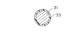
スペーサー8は、図2に示すように、着色されていない有機質無機質複合体粒子31からなるものであってもよい。このときには、パネルに振動や衝撃を加えても物理的損傷が起こりにくいし、スペーサー周囲の光抜けの増大が抑制される。このため、コントラストの向上など表示品位の向上ができる。
【0079】
スペーサー8は、図3に示すように、着色されている有機質無機質複合体粒子32からなるものであってもよい。このときには、スペーサー8による光抜けが起こりにくくなるので、輝点が目立たなくなり、表示品位がより向上するという利点がさらに得られる。
【0080】
スペーサー8は、図4に示すように、着色されていない有機質無機質複合体粒子31とこの粒子31表面に形成された接着剤層33とを含むものであってもよい。このときには、スペーサーがさらに移動しにくくなるため、配向膜等の部材の損傷が防がれ、表示品位の向上をより高めるという利点がさらに得られる。
【0081】
スペーサー8は、図5に示すように、着色された有機質無機質複合体粒子32とこの粒子32表面に形成された接着剤層33とを含むものであってもよい。このときには、スペーサー8による光抜けが起こりにくくなるので、輝点が目立たなくなり、表示品位がより向上するという利点と、スペーサーが移動しにくくなるため、配向膜等の部材の損傷が防がれ、表示品位の向上をより高めるという利点とがさらに得られる。
【0082】
導電性粒子は、図6に示すように、有機質無機質複合体粒子34とこの粒子34表面に形成された導体層35とを含む。導体層35は、たとえば、無電解メッキにより形成された金属被膜であり、1層でも2層以上でもよい。
[実施例1]
冷却管、温度計、滴下口のついた4つ口フラスコ中に25%アンモニア水5g、水600gを混合した溶液(A液)を入れ、25±2℃に保持し、攪拌しながらこの溶液中に、β−(3,4−エポキシシクロヘキシル)エチルトリメトキシシラン60g、メタノール160gを混合した溶液(B液)を滴下口から添加して、β−(3,4−エポキシシクロヘキシル)エチルトリメトキシシランの加水分解・縮合を行った。撹拌を継続しながら、1時間後に硬化剤としての2−ジ−n−ブチルアミノ−4,6−ジメルカプト−s−トリアジン5gを滴下口から添加し、さらに1時間撹拌を行った。その後、50℃に昇温し、硬化反応を進めた。
【0083】
加熱を1時間続けた後、室温まで冷却し、硬化粒子の懸濁体を得た。得られた懸濁体を光学顕微鏡で観察したところ粒子間の合着は認められなかった。
次に、この懸濁体を濾過により固液分離し、得られたケーキをメタノールによる洗浄を3回繰り返して行い、得られた硬化粒子を窒素雰囲気下280℃で2時間加熱して複合体粒子(1)を得た。複合体粒子(1)は平均粒子径5.1μm、変動係数3.0%であった。
【0084】
上記で得られた複合体粒子(1)を用いて従来公知の方法によりB版大のTFT型液晶表示板(1)を作製した。液晶表示板(1)は隙間距離が非常に均一化されており、非常に良好な表示品位であった。次に、120℃でアニールした後、液晶表示板(1)に1000回の殴打試験を行い、透過率が5%となるように電圧を印可して、殴打試験前後のスペーサ周囲の光抜け状態を目視で観察したところ、スペーサの移動による配向膜の傷付けによる輝点、及びスペーサー周囲の光抜けの増大はほとんど認められず、隙間距離も均一であり良好な表示品位を維持していた。
[実施例2]
実施例1において硬化剤をジアミノジフェニルメタンに変更した以外は実施例1の操作を繰り返して、複合体粒子(2)を得た。得られた複合体粒子(2)は平均粒子径4.9μm、変動係数3.4%であった。
【0085】
この複合体粒子(2)を用いて従来公知の方法によりB版大のTFT型液晶表示板(2)を作製したところ、実施例1と同様の結果が得られた。
[実施例3]
実施例1において硬化剤をベンジルジメチルアミンに変更した以外は実施例1の操作を繰り返して、複合体粒子(3)を得た。得られた複合体粒子(3)は平均粒子径6.0μm、変動係数3.6%であった。
【0086】
この複合体粒子(3)を用いて従来公知の方法によりB版大のTFT型液晶表示板(3)を作製したところ、実施例1と同様の結果が得られた。
[実施例4]
実施例1において硬化剤を無水ピロメリット酸に変更した以外は実施例1の操作を繰り返して、複合体粒子(4)を得た。得られた複合体粒子(4)は平均粒子径5.3μm、変動係数3.6%であった。
【0087】
この複合体粒子(4)を用いて従来公知の方法によりB版大のTFT型液晶表示板(4)を作製したところ、実施例1と同様の結果が得られた。
[実施例5]
冷却管、温度計、滴下口のついた4つ口フラスコ中に25%アンモニア水5g、水600gを混合した溶液(A液)を入れ、25±2℃に保持し、攪拌しながらこの溶液中に、β−(3,4−エポキシシクロヘキシル)エチルトリメトキシシラン60g、メタノール160gを混合した溶液(B液)を滴下口から添加して、β−(3,4−エポキシシクロヘキシル)エチルトリメトキシシランの加水分解・縮合を行った。撹拌を継続しながら、1時間後に硬化剤としての2−ジ−n−ブチルアミノ−4,6−ジメルカプト−s−トリアジン5gを滴下口から添加し、さらに1時間撹拌を行った。その後、50℃に昇温し、硬化反応を進めた。加熱を1時間続けた後、室温まで冷却し、硬化粒子の懸濁体を得た。
【0088】
次に、この懸濁体を濾過により固液分離し、得られたケーキをメタノールによる洗浄を3回繰り返して行い、得られた硬化粒子を冷却管、温度計、滴下口のついた4つ口フラスコに入れた。次いで滴下口からトルエン100g、及びトリレンジイソシアネート(TDI)10gを加えて、80℃で3時間撹拌を行い、エポキシ基の開環により生成した水酸基のイソシアネートによる硬化反応を行った。撹拌後室温まで冷却し硬化粒子の懸濁体を得た。 次に、この懸濁体を濾過により固液分離し、得られたケーキをトルエンによる洗浄を2回とそれに引き続くメタノールによる洗浄を1回行い、得られた硬化粒子を窒素雰囲気下280℃で2時間加熱して複合体粒子(5)を得た。複合体粒子(5)は平均粒子径5.0μm、変動係数3.7%であった。
【0089】
上記で得られた、複合体粒子(5)を用いて従来公知の方法によりB版大のTFT型液晶表示板(5)を作製したところ、実施例1と同様の結果が得られた。[実施例6]
冷却管、温度計、滴下口のついた4つ口フラスコ中に25%アンモニア水5g、水600gを混合した溶液(A液)を入れ、25±2℃に保持し、攪拌しながらこの溶液中に、β−(3,4−エポキシシクロヘキシル)エチルトリメトキシシラン60g、メタノール160gを混合した溶液(B液)を滴下口から添加して、β−(3,4−エポキシシクロヘキシル)エチルトリメトキシシランの加水分解・縮合を行った。撹拌を継続しながら、1時間後に硬化剤としての3−メルカプトプロピルトリメトキシシラン10gを滴下口から添加し、さらに1時間撹拌を行った。その後、50℃に昇温し、硬化反応を進めた。
【0090】
加熱を1時間続けた後、室温まで冷却し、硬化粒子の懸濁体を得た。得られた懸濁体を光学顕微鏡で観察したところ粒子間の合着は認められなかった。
次に、この懸濁体を濾過により固液分離し、得られたケーキをメタノールによる洗浄を3回繰り返して行い、得られた硬化粒子を窒素雰囲気下280℃で2時間加熱して複合体粒子(6)を得た。複合体粒子(6)は平均粒子径4.8μm、変動係数3.6%であった。
【0091】
上記で得られた、複合体粒子(6)を用いて従来公知の方法によりB版大のTFT型液晶表示板(6)を作製したところ、実施例1と同様の結果が得られた。[実施例7]
酸性染料であるKayacyl Sky Blue R(日本化薬(株)製)4gを水100gに溶解した溶液と、実施例1で得られた複合体粒子(1)15gを水500gに分散した分散液とを混合し、オートクレーブ中で150℃で1時間加圧加熱処理した。処理後、濃青色に着色された粒子を濾過で捕集し、更に水洗を3回繰り返した後、200℃で真空乾燥して濃青色に着色された複合体粒子(7)を得た。複合体粒子(7)は平均粒子径5.0μm、変動係数3.8%であった。
【0092】
この複合体粒子(7)を用いて従来公知の方法によりB版大のSTN型液晶表示板(7)を作製したところ、実施例1と同様の結果が得られるとともに、輝点(光抜け)が少なかった。
[実施例8]
塩基性染料であるKayacryl Black NP200(日本化薬(株)製)4gを水250gに溶解し、酢酸を加えてpHを4とした後、実施例1で得られた複合体粒子(1)10gを加えて良く撹拌しながら95℃で8時間加熱して黒色に着色された複合体粒子(8)を得た。複合体粒子(8)は平均粒子径4.9μm、変動係数4.1%であった。
【0093】
この複合体粒子(8)を用いて従来公知の方法によりB版大のSTN型液晶表示板(8)を作製したところ、実施例7と同様の結果が得られた。
[実施例9]
実施例1において、A液に塩基性染料であるKayacryl Black NP200(日本化薬(株)製)3gを加えたこと以外は実施例1の操作を繰り返して、黒色に着色された複合体粒子(9)を得た。複合体粒子(9)は平均粒子径5.2μm、変動係数4.0%であった。
【0094】
この複合体粒子(9)を用いて従来公知の方法によりB版大のSTN型液晶表示板(9)を作製したところ、実施例7と同様の結果が得られた。
[実施例10]
実施例1で得られた複合体粒子(1)30gと熱可塑性樹脂粒子(メチルメタクリレート84wt%とn−ブチルアクリレート16wt%との共重合体、ガラス転移温度70℃、平均粒子径0.3μm)1gとを混合し、更に奈良機械製作所製ハイブリダイゼーションシステムNHS−0型を使用して複合体粒子(1)の表面を熱可塑性樹脂で被覆して表面に接着層を有する複合体粒子(10)を得た。得られた接着層を有する複合体粒子(10)をSEM観察したところ複合体粒子(10)の表面は完全に熱可塑性樹脂で被覆されており、その断面をTEMで観察したところ、被覆層の厚みは0.08μmであった。
【0095】
この複合体粒子(10)を用いて従来公知の方法によりB版大のTFT型液晶表示板(10)を作製した。液晶表示板(10)は隙間距離が非常に均一化されており、非常に良好な表示品位であった。次に120℃でアニールした後、液晶表示板(10)に1000回の殴打試験を行い、透過率が5%となるように電圧を印可して、殴打試験前後のスペーサ周囲の光抜け状態を目視で観察したところ、スペーサの移動による配向膜の傷付けによる輝点、及びスペーサー周囲の光抜けの増大はほとんど認められず、隙間距離も均一であり良好な表示品位を維持していた。
[実施例11]
実施例10において、複合体粒子(1)の代わりに実施例9で得られた複合体粒子(9)を使用したこと以外は実施例10の操作を繰り返して、表面に接着層を有する黒色に着色された複合体粒子(11)を得た。得られた接着層を有する複合体粒子(11)をSEM観察したところ複合体粒子(11)の表面は完全に熱可塑性樹脂で被覆されており、その断面をTEMで観察したところ、被覆層の厚みは0.08μmであった。
【0096】
この複合体粒子(11)を用いて従来公知の方法によりB版大のSTN型液晶表示板(11)を作製したところ、実施例10と同様の結果が得られるとともに、輝点(光抜け)が少なかった。
[実施例12]
実施例1で得られた複合体粒子(1)に無電解Niメッキを施した後、さらに無電解金メッキを施し、導電性粒子(12)を得た。得られた導電性粒子(12)は平均粒子径5.9μm、変動係数4.2%であった。得られた導電性粒子(12)をSEM及びXMAで観察したところ、導電性粒子(12)の表面は完全にNiでメッキ被覆され、その上に金でメッキ被覆されており、その断面をTEMで観察したところ、被覆層の厚みは0.3μmであった。導電性粒子(12)のメッキ層の密着性を下記の手法で評価したところ、評価結果は○であり、非常に良好な耐剥離性を示した。
<導電性粒子のメッキ層の密着性の評価方法>
導電性粒子とジルコニアビーズ90gをマヨネーズ瓶に入れ、ホールピペットでヘキサン10mlを加える。次にペイントシェーカーで10分間振とうを行い、終了後、ピペットで試料溶液を吸い上げ、金属顕微鏡で観察し最もメッキ層剥離の激しい視野を観察し、その剥離数から下記の判定基準で判定する。
【0097】
メッキ層の剥離した粒子数:1個…○,2〜10個…△,10個以上…×
[比較例1]
冷却管、温度計、滴下口のついた4つ口フラスコに25%アンモニア水5g、水600gを混合した溶液(A液)を入れ、25±2℃に保持し、攪拌しながらこの溶液中に、β−(3,4−エポキシシクロヘキシル)エチルトリメトキシシラン60g、メタノール160gを混合した溶液(B液)を滴下口から添加して、β−(3,4−エポキシシクロヘキシル)エチルトリメトキシシランの加水分解・縮合を行った。硬化剤を加えずに撹拌を2時間行った後、50℃に昇温した。
【0098】
加熱を1時間続けた後、室温まで冷却し得られた懸濁体を光学顕微鏡で観察したところ粒子間の合着が多数認められた。
[比較例2]
冷却管、温度計、滴下口のついた4つ口フラスコ中に25%アンモニア水2.9g、メタノール10.1g、水141.1gを混合した溶液(A液)を入れ、25±2℃に保持し、攪拌しながらこの溶液中に、γ−メタクリロキシプロピルトリメトキシシラン27g、メタノール54g、ラジカル重合開始剤として2,2′−アゾビス(2,4−ジメチルバレロニトリル)0.14gを混合した溶液(B液)を滴下口から添加して、γ−メタクリロキシプロピルトリメトキシシランの加水分解・縮合を行った。撹拌を継続しながら、20分後、窒素雰囲気中で70±5℃に加熱し、ラジカル重合を行った。
【0099】
加熱を2時間続けた後、室温まで冷却し、重合体粒子の懸濁体を得た。懸濁体を濾過により固液分離し、得られたケーキをメタノールによる洗浄を3回繰り返して行い、得られた重合体粒子を窒素雰囲気下200℃で2時間加熱して比較複合体粒子(2)を得た。比較複合体粒子(2)は平均粒子径4.2μm、変動係数3.8%であった。
【0100】
比較複合体粒子(2)を用いて実施例1と同様の方法により作製したB版大のTFT型液晶表示板の1000回の殴打試験前後のスペーサー周囲の光抜けの程度、スペーサーの移動による配向膜の傷付けによる輝点の程度、及び表示品位を目視で評価した。結果を表1に示す。比較複合体粒子(2)では1000回殴打試験前後の性能が複合体粒子(1)よりも劣っていた。
[比較例3]
比較例2で得られた比較複合体粒子(2)に無電解Niメッキを施した後、さらに無電解金メッキを施し、比較導電性粒子(3)を得た。得られた比較導電性粒子(3)は平均粒子径4.51μm、変動係数4.2%であった。得られた比較導電性粒子(3)をSEM及びXMAで観察したところ、比較導電性粒子(3)の表面は完全にNiでメッキ被覆され、その上に金でメッキ被覆されており、その断面をTEMで観察したところ、被覆層の厚みは0.47μmであった。比較導電性粒子(3)のメッキ層の密着性を上記の手法で評価したところ、評価結果は△であり、導電性粒子(11)よりは劣った性能であった。
【0101】
【表1】
【発明の効果】
本発明の有機質無機質複合体粒子は、原料として、従来技術の重合性不飽和基を有するシリコン化合物に代えて、エポキシ基を有するシリコン化合物を用いるので、得られる粒子の表面にはエポキシ基に由来する水酸基やエーテル結合と、エポキシ基の硬化剤に由来するアミノ基、エステル結合、チオエーテル結合等の官能基が存在しており、ポリイミド等の材質からなる液晶配向膜等に対する付着性が高い。
【0103】
本発明にかかる有機質無機質複合体粒子の製造方法は、粒子間の合着が起こらず、粒子径分布の狭い、前記有機質無機質複合体粒子を簡便にかつ歩留まり良く製造することができる。
【0104】
本発明の導電性粒子は、粒子の表面にエポキシ基に由来する水酸基やエーテル結合と、エポキシ基の硬化剤に由来するアミノ基、エステル結合、チオエーテル結合等の官能基が存在するため、粒子表面に親水性が付与されており、粒子表面と導体層との密着性に優れるため、一対の電極間の隙間距離を一定に保持しやすく、加圧による導体層の剥がれ落ち・電気的に接続されるべきではない電極間のショート・電気的に接続されるべき電極間の接触不良が起こらず、接着信頼性が高い。このためエレクトロニクスの実装材料として有用である。
【0105】
本発明の液晶表示板用スペーサーは、上記有機質無機質複合体粒子からなるので、正確な間隔で配置されるべき1対の電極基板間の隙間距離を一定に保持することができるとともに、液晶配向膜等への付着性が高く、強い衝撃や振動を受けても電極基板や配向膜等に対して物理的損傷を与えることがない。また、スペーサーが移動しにくく、配向膜の傷付けによる輝点の発生や粒子周囲の光抜けの増大を抑制するため、液晶表示板の画質向上を図ることができる。
【図面の簡単な説明】
【図1】 本発明の液晶表示板の1実施例を表す部分断面図である。
【図2】 本発明の液晶表示板用スペーサーの1実施例を表す断面図である。
【図3】 本発明の液晶表示板用スペーサーの1実施例を表す断面図である。
【図4】 本発明の液晶表示板用スペーサーの1実施例を表す断面図である。
【図5】 本発明の液晶表示板用スペーサーの1実施例を表す断面図である。
【図6】 本発明の導電性粒子の1実施例を表す断面図である。
【符号の説明】
2 接着シール材
3 シール部スペーサー
4 配向膜
5 電極
6 偏光膜
7 液晶
8 面内スペーサー
11 下側ガラス基板
12 上側ガラス基板
31 有機質無機質複合体粒子
32 有機質無機質複合体粒子
33 接着剤層
34 有機質無機質複合体粒子
35 導体層
110 下側電極基板
120 上側電極基板[0001]
BACKGROUND OF THE INVENTION
The present invention relates to organic-inorganic composite particles, a method for producing the same, and uses.
[0002]
[Prior art]
A liquid crystal display panel (LCD) is composed of two opposing electrode substrates, a spacer interposed between the electrode substrates, and a liquid crystal substance. The spacer is used to keep the thickness of the liquid crystal layer uniform and constant.
[0003]
Display performance required for practical use of a liquid crystal display panel generally includes high-speed response, high contrast, wide viewing angle, and the like. In order to realize these various performances, the thickness of the liquid crystal layer, that is, the gap distance between the two electrode substrates must be kept strictly constant.
[0004]
As a spacer for a liquid crystal display panel according to such a request, silica particles produced by a sol-gel method (Japanese Patent Laid-Open No. 62-269933), and those obtained by firing the silica particles (Japanese Patent Laid-Open No. 1-234826) ), Styrene-based or divinylbenzene-based polymer particles obtained by suspension polymerization of styrene-based monomers or divinylbenzene-based monomers (JP-A 61-95016), polymerizable unsaturated groups and alkoxysilyl There are organic-inorganic composite particles (JP-A-8-81561) obtained by subjecting a silane compound having a group to hydrolysis / condensation / polymerization and then heat treatment. These are all spherical particles having a narrow particle size distribution and a well-equipped particle size.
[0005]
Among these, the organic-inorganic composite particles are less likely to aggregate, and the mechanical resilience necessary to maintain a constant gap distance between a pair of members that should be arranged at an accurate interval such as a liquid crystal display panel. And a strength required to keep the gap distance constant with a small number. However, when organic-inorganic composite particles are used as spacers for liquid crystal display panels, the spacers are easy to move because of their low adhesion to the liquid crystal alignment film made of polyimide, etc. There is a problem in that omission increases and display quality decreases. In addition, when a conductive layer is provided on the particle surface and used as a conductive particle, the adhesion between the particle surface and the conductive layer is low, and the conductive layer should not be peeled off or electrically connected by pressurization. There is a problem that a short circuit between the electrodes and a contact failure between the electrodes to be electrically connected occur.
[0006]
[Problems to be solved by the invention]
Therefore, the problem to be solved by the present invention is that even when subjected to impact or vibration, physical damage to the electrode substrate or the liquid crystal alignment film is difficult, the adhesion to the liquid crystal alignment film such as polyimide is high, and the particle size An organic-inorganic composite particle having a narrow distribution and no aggregation, a method for producing the same, and an application thereof are provided.
[0007]
[Means for Solving the Problems]
In order to solve the above problems, the present invention provides the following configurations.
(1) General formula (1)
[0008]
[Chemical 3]
(Where R 1 Represents a monovalent organic group having an epoxy group, R 2 Represents at least one monovalent organic group selected from the group consisting of a hydrogen atom, an alkyl group having 1 to 5 carbon atoms and an acyl group having 2 to 5 carbon atoms; Three Represents at least one monovalent organic group selected from the group consisting of an alkyl group having 1 to 5 carbon atoms and a phenyl group. X + Y + Z = 4, X is 1 or 2, Y is 2 or 3, and Z is 0 or 1. )
Hydrolysis / condensation of at least one first silicon compound selected from the group consisting of a compound represented by: 1 Organic-inorganic composite particles obtained by curing an epoxy group inside with a curing agent.
(2) a condensation step of hydrolyzing and condensing at least one first silicon compound selected from the group consisting of the compound represented by the above general formula (1) and derivatives thereof;
R during and / or after the condensation step 1 A method for producing organic-inorganic composite particles, comprising a curing step of curing an epoxy group therein with a curing agent.
(3) Conductive particles comprising the organic-inorganic composite particles according to (1) as a main body and a conductor layer formed on the surface thereof.
(4) A spacer for a liquid crystal display panel comprising the organic-inorganic composite particles according to (1) as a main body.
(5) A liquid crystal display panel using the liquid crystal display panel spacer described in (4) above as a spacer interposed between electrode substrates.
[0010]
DETAILED DESCRIPTION OF THE INVENTION
[Organic inorganic composite particles and method for producing the same]
The method for producing organic-inorganic composite particles of the present invention includes a condensation step and a curing step.
[0011]
The condensation step is represented by the general formula (1)
[0012]
[Formula 4]
(Where R 1 Represents a monovalent organic group having an epoxy group, R 2 Represents at least one monovalent organic group selected from the group consisting of a hydrogen atom, an alkyl group having 1 to 5 carbon atoms and an acyl group having 2 to 5 carbon atoms; Three Represents at least one monovalent organic group selected from the group consisting of an alkyl group having 1 to 5 carbon atoms and a phenyl group. X + Y + Z = 4, X is 1 or 2, Y is 2 or 3, and Z is 0 or 1. )
And hydrolyzing and condensing at least one first silicon compound selected from the group consisting of a compound represented by the formula:
[0014]
In the condensation step, the following second silicon compound can be used in combination with the first silicon compound. The second silicon compound has the following general formula (2):
[0015]
[Chemical formula 5]
(Where R Four Represents at least one group selected from the group consisting of an alkyl group, an aryl group and an unsaturated aliphatic residue, and the group may have a substituent; R Five Represents at least one monovalent group selected from the group consisting of a hydrogen atom, an alkyl group having 1 to 5 carbon atoms, and an acyl group having 2 to 5 carbon atoms; n represents an integer of 0 to 2) Or at least one selected from the group consisting of derivatives thereof.
[0017]
In the general formulas (1) and (2), the hydrolyzable group is R 2 O, R Five O and at least one monovalent organic group selected from the group consisting of a hydroxyl group, an alkoxy group having 1 to 5 carbon atoms, and an acyloxy group having 2 to 5 carbon atoms. In the general formulas (1) and (2), R 2 The number (Y) of O groups is 2 or 3, and R Five The number of O groups (4-n) is 2 to 4, but may be different from each other, or two or more may be the same. Preferred R 2 O group, R Five The O group is a methoxy group, an ethoxy group, a propoxy group, or an acetoxy group, with a high hydrolysis / condensation rate, and a methoxy group and an ethoxy group are more preferable. The first silicon compound and the second silicon compound are R 2 O group, R Five The O group is hydrolyzed with water and further condensed to form a polysiloxane skeleton.
[0018]
In the general formula (1), R 1 Is a monovalent organic group having an epoxy group. In the general formula (1), R 1 The number of (X) is one or two, but in the case of two, they may be different from each other or the same. R 1 The number of epoxy groups contained in may be two or more. R 1 The type of is not particularly limited, but it is possible to obtain particles having a sharp particle size distribution by preventing aggregation of the particles, and also because of high adhesion to a liquid crystal alignment film made of polyimide or the like, an epoxycyclohexyl group, glycidoxy. A C1-C20 monovalent organic group having a group is preferred.
[0019]
In the general formula (1), R Three Is at least one monovalent organic group selected from an alkyl group having 1 to 5 carbon atoms and a phenyl group. R Three Examples thereof include a methyl group, an ethyl group, and a propyl group, and a methyl group and an ethyl group are preferable from the viewpoint of preventing aggregation of particles and obtaining particles having a sharp particle size distribution.
[0020]
Specific examples of the compound represented by the general formula (1) include β- (3,4-epoxycyclohexyl) ethyltrimethoxysilane, 3,4-epoxybutyltrimethoxysilane, and γ-glycidoxypropyltrimethoxysilane. Γ-glycidoxypropylmethyldiethoxysilane, γ-glycidoxypropylmethyldimethoxysilane, γ-glycidoxypropyltriethoxysilane, and the like.
[0021]
In the general formula (2), R Four Represents at least one group selected from the group consisting of an alkyl group, an aryl group, and an unsaturated aliphatic residue, and the group may have a substituent. In the general formula (2), R Four The number (n) of is from 0 to 2, but in the case of two, they may be different from each other or the same.
[0022]
Specific examples of the compound represented by the general formula (2) include tetrafunctional silanes such as tetramethoxysilane, tetraethoxysilane, tetraisopropoxysilane, tetrabutoxysilane, and tetraacetoxysilane, where n = 0. Silane; methyltrimethoxysilane, methyltriethoxysilane, ethyltrimethoxysilane, ethyltriethoxysilane, phenyltrimethoxysilane, methyltriacetoxysilane, vinyltrimethoxysilane, 3- (meth) acryloxypropyltrimethoxysilane, etc. General formula (2) of general formula (2), such as trifunctional silane of n = 1; dimethyldimethoxysilane, dimethyldiethoxysilane, 3- (meth) acryloxypropylmethyldimethoxysilane, diacetoxydimethylsilane, diphenyldisilanediol, etc. 2) n = They include bifunctional silane of.
[0023]
Examples of the derivatives of the compounds represented by the general formulas (1) and (2) include, for example, some Rs of the compounds represented by the general formulas (1) and (2) 2 O group and R Five Compounds in which the O group is substituted with a β-dicarbonyl group and / or a group capable of forming another chelate compound; compounds represented by the general formulas (1) and (2) and / or chelate compounds thereof are partially Examples thereof include a low condensate obtained by hydrolysis / condensation.
[0024]
These first silicon compound and second silicon compound may be used alone or in combination of two or more.
The amount of the second silicon compound is not particularly limited, but when used in a large amount, the shape of the organic-inorganic composite particles obtained may not be spherical, it may be difficult to control the particle size, or the particle size distribution may be Since it may spread, it is preferably 1 to 50% by weight, more preferably 5 to 25% by weight, based on the first silicon compound.
[0025]
In the condensation step, the first silicon compound and the second silicon compound used as necessary (hereinafter, both may be collectively referred to as “raw materials”) are hydrolyzed in a solvent containing water. And condensed. Hydrolysis and condensation can take any method such as batch, split, and continuous. For hydrolysis or condensation, a catalyst such as ammonia, urea, ethanolamine, tetramethylammonium hydroxide, alkali metal hydroxide, or alkaline earth metal hydroxide may be used. In the solvent, an organic solvent other than water and the catalyst may be present. Specific examples of the organic solvent include methanol, ethanol, isopropanol, n-butanol, isobutanol, sec-butanol, t-butanol, pentanol, ethylene glycol, propylene glycol, 1,4-butanediol and other alcohols; acetone Ketones such as methyl ethyl ketone; esters such as ethyl acetate; (cyclo) paraffins such as isooctane and cyclohexane; ethers such as dioxane and diethyl ether; aromatic hydrocarbons such as benzene and toluene alone or , Mixed and used.
[0026]
Hydrolysis and condensation are performed, for example, by adding the above-described raw material or an organic solvent solution thereof to a solvent containing water and stirring at 0 to 100 ° C., preferably 0 to 70 ° C. for 30 minutes to 100 hours. .
[0027]
Alternatively, the particles obtained by the method described above may be charged in advance in the synthesis system as seed particles, and the seed particles may be grown by adding the raw materials.
In this manner, the raw material is hydrolyzed and condensed under a suitable condition in a solvent containing water, whereby particles are precipitated and a slurry is generated. The precipitated particles are particles having an average particle size of 0.5 μm or more and a sharp particle size distribution. Here, as appropriate conditions, for example, a raw material concentration of 30% by weight or less, a water concentration of 50% by weight or more, and a catalyst concentration of 10% by weight or less are preferably used for the obtained slurry.
[0028]
For example, the water concentration, the catalyst concentration, the organic solvent concentration, the raw material concentration, the raw material addition time, the temperature, and the seed particle concentration are set to, for example, 50 to 99.99 wt%, 0.01 to 10 wt%, and 0 to 0, respectively. By setting 90% by weight, 0.1 to 30% by weight, 0.001 to 500 hours, 0 to 100 ° C., and 0 to 10% by weight, the average particle size of particles generated by hydrolysis and condensation is described later. Can be within the range. Further, by setting the water concentration, the catalyst concentration, and the organic solvent concentration within the above ranges, the coefficient of variation of the particle diameter of the generated particles can be set within the ranges described below.
[0029]
The curing process is R 1 This is a step of curing the epoxy group therein with a curing agent, whereby an organic polymer skeleton is formed. In the case where the epoxy group is not cured by the curing agent, the cross-linking formation in the particles becomes insufficient, so that coalescence between the particles is likely to occur and aggregates are generated. By curing with a curing agent, coalescence of particles can be prevented and monodispersed particles can be obtained. The curing step may be before the condensation step, during the condensation step, or after the condensation step, but is preferably during the condensation step and / or after the condensation step. That is, it is preferable to cure the epoxy group of the intermediate product / particle obtained by hydrolysis / condensation of the raw material containing the first silicon compound with a curing agent.
[0030]
Examples of curing with a curing agent include (1) a polyaddition reaction by ring opening of an epoxy group and (2) a reaction in which an epoxy group is ionically ring-opened and added by a catalyst.
[0031]
Examples of the curing agent for performing the polyaddition reaction by ring opening of the epoxy group of (1) include a compound having active hydrogen, and the compound may have a hydrolyzable silyl group. When the curing agent has a hydrolyzable silyl group, in addition to the reaction between the epoxy group and the curing agent, silanol groups and / or alkoxysilyl groups present in the particles before curing and the hydrolyzable silyl group in the curing agent Curing by condensation with is performed. Moreover, when it has two or more organic groups which have active hydrogen which reacts with an epoxy group in a hardening | curing agent, they may mutually be the same and may differ. Examples of the curing agent having active hydrogen include, but are not limited to, compounds having an amino group, a carboxylic acid anhydride, a hydroxyl group, a mercapto group, and the like.
[0032]
Examples of the curing agent having an amino group include polyamines such as diethylenetriamine, triethylenetetramine, isophoronediamine, m-xylenediamine, diaminodiphenylmethane, diaminodiphenylsulfone, melamine, and diallylmelamine; alcohols such as monoethanolamine, diethanolamine, and propanolamine Examples include amines.
[0033]
Examples of the curing agent having a carboxylic acid anhydride include phthalic anhydride, maleic anhydride, pyromellitic anhydride, benzophenone tetracarboxylic anhydride, trimellitic anhydride, pimelic acid, and the like.
[0034]
Examples of the curing agent having a hydroxyl group include bisphenol A and phenol novolac.
Examples of the curing agent having a mercapto group include trioxane trimethylene mercaptan, triazine trithiol, triazine dithiols, polysulfide and the like.
[0035]
Examples of the compound having an organic group capable of reacting with an epoxy group and a hydrolyzable silyl group include a compound having an amino group and a hydrolyzable silyl group, and a compound having a mercapto group and a hydrolyzable silyl group. Illustrated.
[0036]
Examples of the compound having an amino group and a hydrolyzable silyl group include a trifunctional silane compound having three hydrolyzable silyl groups such as 3-aminopropyltrimethoxysilane, 3-aminopropyltriethoxysilane, and the like. Bifunctional silane compounds having two hydrolyzable silyl groups such as propylmethyldiethoxysilane, N- (2-aminoethyl) -3-aminopropylmethyldimethoxysilane, and hydrolysis of 3-aminopropyldimethylethoxysilane And monofunctional silane compounds having one functional silyl group.
[0037]
Examples of the compound having a mercapto group and a hydrolyzable silyl group include trifunctional compounds having three hydrolyzable silyl groups such as mercaptomethyltrimethoxysilane, 3-mercaptopropyltriethoxysilane, and 3-mercaptopropyltrimethoxysilane. Examples thereof include bifunctional silane compounds having two hydrolyzable silyl groups such as a silane compound, mercaptomethyldiethoxysilane, and 3-mercaptopropylmethyldimethoxysilane.
[0038]
Of these compounds having an organic group capable of reacting with an epoxy group and a hydrolyzable silyl group, trifunctional and bifunctional compounds are preferred for sufficiently carrying out the curing reaction.
[0039]
As the curing agent for ionically ring-opening-addition polymerization of the epoxy group of (2), a compound that polymerizes an epoxy group such as tertiary amines and imidazoles by anionic polymerization and an epoxy group such as Lewis acid are used. Examples include compounds that are polymerized by cationic polymerization.
[0040]
Examples of the tertiary amines include benzyldimethylamine, 2- (dimethylaminomethyl) phenol, 2,4,6-tris (dimethylaminomethyl) phenol, and the like.
[0041]
Examples of the imidazoles include 2-methylimidazole, 2-phenylimidazole, 2-ethyl-4-methylimidazole, and the like.
Examples of the Lewis acid include boron trifluoride / amine complex.
[0042]
The amount of the curing agent is preferably 0.1 to 80% by weight, more preferably 1 to 50% by weight, based on the raw material (total amount of the first silicon compound and the second silicon compound). When it is less than the above range, the epoxy group is not sufficiently cured, and coalescence between particles tends to occur. On the other hand, if it exceeds the above range, a large amount of excess curing agent is generated, and it takes time to clean the particles after the curing step.
[0043]
As a method of curing the epoxy group, a curing agent may be added and dissolved in a solvent slurry containing water of particles obtained by hydrolysis / condensation and cured as it is, or by hydrolysis / condensation. The obtained particles are isolated from the slurry using a conventionally known method such as filtration, centrifugal separation, vacuum concentration, etc., and then dispersed in a solution containing a curing agent or an organic solvent to be cured. Well, it is not limited to these. Particularly preferred is a method in which after curing and condensing the above raw materials, a curing reaction is carried out in the presence of a curing agent in the reaction system. Further, the curing reaction may be further performed with a curing agent capable of reacting the hydroxyl group generated by ring opening of the epoxy group in the cured particle obtained by the above method with the hydroxyl group. Examples of the curing agent capable of reacting with a hydroxyl group include compounds having two or more isocyanate groups, and specific examples include tolylene diisocyanate, isophorone diisocyanate, and hexamethylene diisocyanate.
[0044]
The organic inorganic composite fine particles having excellent adhesion of the present invention can be obtained by the condensation step and the curing step, but the produced particles are isolated from the slurry using a conventionally known method such as filtration, centrifugation, and vacuum concentration. After that, heat treatment may be performed. The heat treatment is preferably performed at a temperature of 800 ° C. or less, more preferably at a temperature of 100 to 600 ° C., and even more preferably at a temperature of 150 to 500 ° C. for drying and firing. Here, when heat treatment is performed at a low temperature, the dehydration condensation reaction between silanol groups present in the siloxane unit does not occur sufficiently, and thus the required strength may not be obtained.
[0045]
Although the atmosphere during the heat treatment can be used without any limitation, it is more preferable that the oxygen concentration in the atmosphere is 10% by volume or less in order to suppress the decomposition of the organic polymer and obtain the necessary mechanical restoration. When the heat treatment temperature is in the range of 200 ° C. to 800 ° C., the oxygen concentration in the atmosphere during the heat treatment is preferably 10% by volume or less in order to obtain organic-inorganic composite particles, and the heat treatment temperature is 200 ° C. or less. If so, organic-inorganic composite particles can be obtained even in the air. Further, the heat treatment may be performed under reduced pressure. Colored organic-inorganic composite particles are obtained by coloring the generated particles during and / or after at least one step selected from a condensation step, a curing step and a heat treatment step. That is, the production method of the present invention produces colored organic-inorganic composite particles by introducing a dye and / or pigment into the particles in the presence of a dye and / or pigment in an appropriate process during production. Can do.
[0046]
In the case of coloring, the color of the organic-inorganic composite fine particles is preferably a color that does not transmit light. A color that does not transmit light is preferable as a color of a spacer for a liquid crystal display panel because light leakage can be prevented and contrast of image quality can be improved. Examples of the color that does not transmit light include black, dark blue, amber, purple, blue, dark green, green, brown, red, and the like, with black, dark blue, and amber being particularly preferable. The dye is appropriately selected and used according to the color to be colored, and examples thereof include disperse dyes, acid dyes, basic dyes, reactive dyes, sulfur dyes and the like classified according to the dyeing method. Specific examples of these dyes are the pages from 1399 to 1427 of the “Chemical Handbook Applied Science Edition, Chemical Society of Japan” (published by Maruzen Co., Ltd., 1986), “Nippon Kayaku Dye Handbook” (published by Nippon Kayaku Co., Ltd. )It is described in.
[0047]
Examples of the dye and dyeing color include those described above. Of these, basic dyes are preferred. This is because since the silanol group in the polysiloxane is acidic, the basic (cationic) dye is easily adsorbed and dyed easily. Examples of the pigment include inorganic pigments such as carbon black, iron black, chromium vermilion, molybdenum red, red pepper, yellow lead, chromium green, cobalt green, ultramarine blue, and bitumen; organic pigments such as phthalocyanine, azo, and quinacridone is there. However, since the pigment may not be introduced into the organic-inorganic composite fine particles of the present invention unless the average particle size is 0.4 μm or less, it is preferable to use a dye.
[0048]
The average particle size of the organic / inorganic composite particles is not particularly limited, but is preferably 0.5 μm or more, more preferably 0.5 to 50 μm, still more preferably 1 to 25 μm, and most preferably 1.5 to 20 μm. is there. When the average particle diameter is less than 0.5 μm, it is difficult to form a gap between a pair of members, and this is a region that is not used as a spacer for liquid crystal display plates and conductive particles described later.
[0049]
When the organic / inorganic composite particles are used as spacers, for example, the variation in particle diameter is preferably 20% or less, more preferably 10% or less, and most preferably 8% or less, from the viewpoint of uniformity of the gap distance between the electrode substrates. Has a coefficient. When the upper limit is exceeded, the uniformity of the gap distance is lowered and image unevenness is likely to occur. The coefficient of variation in particle size is
[0050]
[Expression 1]
Defined by
In the present invention, the average particle size and the standard deviation of the particle size were obtained from the following equation by actually measuring the particle size of 200 arbitrary particles in an electron microscope image.
[0052]
[Expression 2]
The shape of the organic-inorganic composite particles may be any particle shape such as spherical, needle-like, plate-like, scale-like, crushed, bowl-like, eyebrows, and confetti, but is not particularly limited. In order to make the gap distance uniform and constant, a spherical shape is preferable. This is because when the particles are spherical, they have a constant or nearly constant particle size in all or almost all directions.
[0054]
The organic-inorganic composite particles of the present invention are less likely to aggregate, and mechanical resilience necessary to maintain a constant gap distance between a pair of members that should be arranged at an accurate interval, such as a liquid crystal display panel, It has the strength necessary to keep the gap distance constant with a small number. Moreover, since a silicon compound having an epoxy group is used as a raw material instead of the silicon compound having a polymerizable unsaturated group of the prior art, a hydroxyl group or an ether bond derived from the epoxy group and an epoxy group are formed on the surface of the obtained particles. Since there are functional groups such as amino groups, ester bonds, and thioether bonds derived from the group curing agent, the adhesion to the liquid crystal alignment film made of polyimide and the like is improved. Hard to cause physical damage to membranes.
[Conductive particles]
The electroconductive particle of this invention makes the main body the organic-inorganic composite particle | grains obtained above, and has a conductor layer on the surface.
[0055]
The conductive particles of the present invention have the above-described organic-inorganic composite particles of the present invention as a main body, and hydroxyl groups and ether bonds derived from epoxy groups on the surface of the particles, and amino groups and ester bonds derived from epoxy group curing agents. , A functional group such as a thioether bond is present, and hydrophilicity is imparted to the particle surface. Therefore, the adhesion between the particle surface and the conductor layer is excellent, it is easy to keep the gap distance between a pair of electrodes constant, the conductor layer is peeled off by pressurization, and the short between electrodes that should not be electrically connected・ No poor contact between electrodes to be electrically connected.
[0056]
Examples of the metal used for the conductor layer include conventionally known metals, such as nickel, gold, silver, copper, indium, and alloys thereof. In particular, nickel, gold, and indium are conductive. It is preferable because it is high. The thickness of the conductor layer is not particularly limited as long as there is sufficient conduction, but the range of 0.01 to 5 μm is preferable, and the range of 0.02 to 2 μm is particularly preferable. If the thickness is less than the above range, the conductivity may be insufficient, and if it is greater than the above range, the conductor layer is likely to be peeled off due to the difference in thermal expansion coefficient between the particles and the conductor layer. The conductor layer may be one layer or two or more layers, and in the case of two or more layers, layers made of different conductors may be arranged above and below.
[0057]
As a method for forming the conductor layer on the surface of the organic / inorganic composite particles, a conventionally known method is used and is not particularly limited. For example, a chemical plating (electroless plating) method, a coating method, PVD (vacuum deposition, sputtering, Among them, the chemical plating method is preferable because the conductive particles of the present invention can be easily obtained.
[0058]
The conductive particles of the present invention are particularly useful as electrical connection materials for electronics such as liquid crystal display boards, LSIs, and printed wiring boards.
[Liquid crystal panel spacer]
The spacer for a liquid crystal display panel of the present invention has the organic-inorganic composite particles obtained above as the main body.
[0059]
Since the spacer for a liquid crystal display panel of the present invention is substantially composed of the organic-inorganic inorganic composite particles, it is difficult to agglomerate, and a gap distance between a pair of members that should be arranged at an accurate interval such as a liquid crystal display panel is set. It has the mechanical resilience necessary to keep it constant, and the strength necessary to keep the gap distance constant with a small number. Moreover, there are hydroxyl groups and ether bonds derived from epoxy groups, and amino groups, ester bonds, thioether bonds, and other functional groups derived from epoxy curing agents, and functional groups present in materials such as polyimide. Since the interaction is strong, the adhesion to the liquid crystal alignment film made of polyimide or the like is high, and the spacer is difficult to move. Therefore, when subjected to impact or vibration, there is no physical damage to members such as the electrode substrate and alignment film, and the generation of bright spots due to the movement of the spacer and the increase of light leakage around the particles are caused. Therefore, the image quality of the liquid crystal display panel can be improved.
[0060]
When the organic / inorganic composite particles are colored by containing a dye and / or pigment, the spacer for a liquid crystal display panel of the present invention is useful as a colored spacer.
[0061]
In the liquid crystal display panel, when a voltage is applied between the electrode substrates, the liquid crystal undergoes an optical change to form an image. On the other hand, the spacer does not show an optical change by voltage application. Therefore, in a dark part when an image is displayed, an uncolored spacer causes light leakage and may be confirmed as a bright spot, which may lower the image quality contrast. When the organic-inorganic composite particles that substantially constitute the spacer for a liquid crystal display panel of the present invention are colored with a dye and / or a pigment, light leakage hardly occurs and image quality contrast hardly decreases. A preferred color of the colored spacer for the liquid crystal display panel is a color that does not easily transmit light or does not transmit light. For example, black, dark blue, amber, purple, blue, dark green, green, brown, red, and the like can be mentioned, and black, dark blue, and amber are particularly preferable.
[0062]
Although the organic / inorganic composite particles of the present invention have excellent adhesion by themselves, a spacer for a liquid crystal display panel having an adhesive layer formed on the surface thereof by coating or chemical bonding is useful as an adhesion spacer. is there. For example, the adhesive layer may exhibit adhesiveness when heated.
[0063]
The adhesive spacer melts and adheres to the electrode substrate when heated and pressurized, and adheres to the electrode substrate when the adhesive layer cools and solidifies. Since the adhesive spacer is difficult to move in the gap between the electrode substrates due to its adhesiveness, it is possible to prevent damage to the alignment film and maintain the uniformity of the gap distance, thereby improving the image quality.
[0064]
As the adhesive layer, a thermoplastic resin is preferable. The glass transition temperature of the thermoplastic resin is preferably 150 ° C. or lower, more preferably 100 ° C. or lower, and even more preferably 80 ° C. or lower. This is because it is bonded to the substrate by heating and pressing for a short time. If the glass transition temperature is too high, it may not adhere to the substrate even if heated. Conversely, if it is too low, the spacers are likely to be fused together, so the temperature is most preferably in the range of 40 to 80 ° C. The type of the thermoplastic resin is not particularly limited, but is preferably a (meth) acrylic resin. The adhesive layer may be one layer or two or more layers, and in the case of two or more layers, layers made of different thermoplastic resins may be arranged one above the other.
[0065]
The adhesive spacer can be obtained, for example, by coating or chemically bonding an adhesive layer on the organic-inorganic composite particles. When a thermoplastic resin is used as an adhesive, specifically, an in situ polymerization method, a coacervation method, an interfacial polymerization method, a submerged curing coating method, a submerged drying method, a high-velocity impact method, an air suspension The surface of the organic-inorganic composite particles of the present invention is coated or chemically bonded with a thermoplastic resin layer by a conventionally known resin coating method such as a coating method or a spray drying method. The high-speed in-air impact method is preferable because it can be easily coated. In the high-speed air impact method, for example, the organic-inorganic composite particles of the present invention and a thermoplastic resin powder are mixed, and the mixture is dispersed in the gas phase to obtain mechanical thermal energy mainly composed of impact force. Is preferably applied to the composite particles and the thermoplastic resin powder by coating the surface of the organic / inorganic composite particles with a thermoplastic resin.
[0066]
Examples of apparatuses utilizing such a high-speed impact in air current method include a hybridization system manufactured by Nara Machinery Co., Ltd., a mechano-fusion system manufactured by Hosokawa Micron Co., Ltd., and a kryptron system manufactured by Kawasaki Heavy Industries, Ltd.
[0067]
The adhesive spacer is particularly useful for improving the image quality of the liquid crystal display panel because it has the characteristics of the organic-inorganic composite particles as described above and has adhesiveness.
Adhesive spacers also have the same effects as described above when colored.
[LCD panel]
The liquid crystal display panel of the present invention is a conventional liquid crystal display panel in which the spacer for a liquid crystal display panel of the present invention as described above is interposed between electrode substrates in place of the conventional spacer. It has the same or almost the same gap distance as the diameter. The amount of spacer used is usually 30-400 pieces / mm 2 , Preferably 50-300 pieces / mm 2 It is.
[0068]
The spacer used in the liquid crystal display panel of the present invention has high adhesion to the alignment film on polyimide or the like, and even when an impact or vibration is applied to the liquid crystal display panel, the movement of the spacer is suppressed, and the electrode substrate or alignment film Physical damage to such members is prevented. In addition, generation of bright spots around the spacer and increase in light leakage due to the movement of the spacer are suppressed, and an improvement in display quality is expected.
[0069]
As shown in FIG. 1, for example, the liquid crystal display element of the present invention includes a
[0070]
In the liquid crystal display panel of the present invention, other than the spacers, electrode substrates, sealing materials, liquid crystals, and the like can be used in the same manner.
The electrode substrate has a substrate such as a glass substrate or a film substrate, and an electrode formed on the surface of the substrate, and an alignment film formed so as to cover the electrode on the surface of the electrode substrate as necessary. Also have. An epoxy resin adhesive sealing material or the like is used as the sealing material. As the liquid crystal, those conventionally used may be used. For example, biphenyl, phenylcyclohexane, Schiff base, azo, azoxy, benzoate, terphenyl, cyclohexylcarboxylate, biphenylcyclohexane , Pyrimidine-based, dioxane-based, cyclohexylcyclohexane ester-based, cyclohexylethane-based, cyclohexene-based, and fluorine-based liquid crystals can be used.
[0071]
As a method for producing the liquid crystal display panel of the present invention, for example, the spacer of the present invention is used as an in-plane spacer and uniformly dispersed on one of the two electrode substrates by a wet method or a dry method. After dispersing the spacer of the present invention as a seal portion spacer in an adhesive seal material such as an epoxy resin, put the one applied by means of screen printing or the like on the adhesive seal portion of the other electrode substrate, and apply an appropriate pressure, Heating at a temperature of 100 to 180 ° C. for 1 to 60 minutes, or irradiation amount of 40 to 300 mJ / cm 2 Examples include a method of injecting liquid crystal and sealing the injection portion after heat-curing the adhesive sealing material by UV irradiation of the above, and obtaining a liquid crystal display plate. Is not limited.
[0072]
In the liquid crystal display panel of the present invention, since the liquid crystal display panel spacer is interposed between the electrode substrates, the gap distance between the electrode substrates is kept constant. In addition, the electrode substrate is not physically damaged by shock or vibration, and the spacer is difficult to move, so there is no problem of bright spots or light leakage around the spacer, and the image quality of the liquid crystal display panel is high. .
[0073]
The liquid crystal display panel of the present invention is used in the same applications as conventional liquid crystal display panels, for example, as image display elements for televisions, monitors, personal computers, word processors, car navigation systems, DVDs, digital video cameras, PHSs (personal digital assistants), etc. used.
[0074]
【Example】
Examples of the present invention and comparative examples outside the scope of the present invention are shown below, but the present invention is not limited to the following examples.
[0075]
The liquid crystal display panels in the following examples were produced by the following method. As shown in FIG. 1, first, an electrode (for example, a transparent electrode) 5 and a polyimide alignment film 4 are formed on a lower glass substrate 11 of 300 mm × 345 mm × 1.1 mm, and then the lower electrode is rubbed. A
[0076]
On the other hand, after forming the electrode (for example, transparent electrode) 5 and the polyimide alignment film 4 on the 300 mm × 345 mm × 1.1 mm
[0077]
Finally, the upper and
[0078]
As shown in FIG. 2, the
[0079]
As shown in FIG. 3, the
[0080]
As shown in FIG. 4, the
[0081]
As shown in FIG. 5, the
[0082]
As shown in FIG. 6, the conductive particles include organic-inorganic
[Example 1]
A solution (liquid A) in which 5 g of 25% aqueous ammonia and 600 g of water were mixed was placed in a four-necked flask equipped with a condenser, a thermometer and a dripping port, and kept at 25 ± 2 ° C. while stirring. A solution (liquid B) prepared by mixing 60 g of β- (3,4-epoxycyclohexyl) ethyltrimethoxysilane and 160 g of methanol was added from the dropping port, and β- (3,4-epoxycyclohexyl) ethyltrimethoxysilane was added. Was hydrolyzed and condensed. While continuing stirring, 5 hours later, 5 g of 2-di-n-butylamino-4,6-dimercapto-s-triazine as a curing agent was added, and stirring was further performed for 1 hour. Then, it heated up at 50 degreeC and advanced hardening reaction.
[0083]
Heating was continued for 1 hour and then cooled to room temperature to obtain a suspension of cured particles. When the obtained suspension was observed with an optical microscope, no coalescence between the particles was observed.
Next, this suspension is subjected to solid-liquid separation by filtration. The obtained cake is washed with methanol three times, and the resulting cured particles are heated at 280 ° C. for 2 hours in a nitrogen atmosphere to form composite particles. (1) was obtained. The composite particles (1) had an average particle size of 5.1 μm and a coefficient of variation of 3.0%.
[0084]
Using the composite particles (1) obtained above, a B-size TFT liquid crystal display panel (1) was prepared by a conventionally known method. The liquid crystal display panel (1) had a very uniform gap distance and a very good display quality. Next, after annealing at 120 ° C., the liquid crystal display panel (1) was subjected to a strike test 1000 times, a voltage was applied so that the transmittance was 5%, and the light leakage around the spacer before and after the strike test. As a result of visual observation, almost no increase in bright spots due to scratches on the alignment film due to movement of the spacers and light leakage around the spacers was observed, the gap distance was uniform, and good display quality was maintained.
[Example 2]
Except that the curing agent was changed to diaminodiphenylmethane in Example 1, the operation of Example 1 was repeated to obtain composite particles (2). The obtained composite particles (2) had an average particle size of 4.9 μm and a coefficient of variation of 3.4%.
[0085]
Using this composite particle (2), a B-size large TFT type liquid crystal display panel (2) was produced by a conventionally known method, and the same results as in Example 1 were obtained.
[Example 3]
Except that the curing agent was changed to benzyldimethylamine in Example 1, the operation of Example 1 was repeated to obtain composite particles (3). The obtained composite particles (3) had an average particle size of 6.0 μm and a coefficient of variation of 3.6%.
[0086]
Using this composite particle (3), a B-size large TFT type liquid crystal display panel (3) was produced by a conventionally known method, and the same results as in Example 1 were obtained.
[Example 4]
Except having changed the hardening | curing agent into pyromellitic anhydride in Example 1, operation of Example 1 was repeated and composite particle | grains (4) were obtained. The obtained composite particles (4) had an average particle size of 5.3 μm and a coefficient of variation of 3.6%.
[0087]
When this composite particle (4) was used to produce a B-size TFT liquid crystal display panel (4) by a conventionally known method, the same results as in Example 1 were obtained.
[Example 5]
A solution (liquid A) in which 5 g of 25% aqueous ammonia and 600 g of water were mixed was placed in a four-necked flask equipped with a condenser, a thermometer and a dripping port, and kept at 25 ± 2 ° C. while stirring. A solution (liquid B) prepared by mixing 60 g of β- (3,4-epoxycyclohexyl) ethyltrimethoxysilane and 160 g of methanol was added from the dropping port, and β- (3,4-epoxycyclohexyl) ethyltrimethoxysilane was added. Was hydrolyzed and condensed. While continuing stirring, 5 hours later, 5 g of 2-di-n-butylamino-4,6-dimercapto-s-triazine as a curing agent was added, and stirring was further performed for 1 hour. Then, it heated up at 50 degreeC and advanced hardening reaction. Heating was continued for 1 hour and then cooled to room temperature to obtain a suspension of cured particles.
[0088]
Next, this suspension is subjected to solid-liquid separation by filtration, and the resulting cake is washed with methanol three times, and the resulting cured particles are transferred to a four-necked tube with a condenser, a thermometer, and a dripping port. Placed in flask. Next, 100 g of toluene and 10 g of tolylene diisocyanate (TDI) were added from the dropping port, and the mixture was stirred at 80 ° C. for 3 hours to carry out a curing reaction of the hydroxyl group generated by ring opening of the epoxy group with isocyanate. After stirring, the mixture was cooled to room temperature to obtain a suspension of cured particles. Next, this suspension is subjected to solid-liquid separation by filtration, and the obtained cake is washed twice with toluene and then once with methanol, and the obtained cured particles are washed at 280 ° C. in a nitrogen atmosphere at 2 ° C. for 2 hours. The composite particles (5) were obtained by heating for a period of time. The composite particles (5) had an average particle size of 5.0 μm and a coefficient of variation of 3.7%.
[0089]
Using the composite particles (5) obtained above, a B-size TFT liquid crystal display panel (5) was produced by a conventionally known method, and the same results as in Example 1 were obtained. [Example 6]
A solution (liquid A) in which 5 g of 25% aqueous ammonia and 600 g of water were mixed was placed in a four-necked flask equipped with a condenser, a thermometer and a dripping port, and kept at 25 ± 2 ° C. while stirring. A solution (liquid B) prepared by mixing 60 g of β- (3,4-epoxycyclohexyl) ethyltrimethoxysilane and 160 g of methanol was added from the dropping port, and β- (3,4-epoxycyclohexyl) ethyltrimethoxysilane was added. Was hydrolyzed and condensed. While continuing stirring, 10 g of 3-mercaptopropyltrimethoxysilane as a curing agent was added from the dropping port after 1 hour, and stirring was further performed for 1 hour. Then, it heated up at 50 degreeC and advanced hardening reaction.
[0090]
Heating was continued for 1 hour and then cooled to room temperature to obtain a suspension of cured particles. When the obtained suspension was observed with an optical microscope, no coalescence between the particles was observed.
Next, this suspension is subjected to solid-liquid separation by filtration. The obtained cake is washed with methanol three times, and the resulting cured particles are heated at 280 ° C. for 2 hours in a nitrogen atmosphere to form composite particles. (6) was obtained. The composite particles (6) had an average particle size of 4.8 μm and a coefficient of variation of 3.6%.
[0091]
Using the composite particles (6) obtained above, a B-size TFT liquid crystal display panel (6) was produced by a conventionally known method, and the same results as in Example 1 were obtained. [Example 7]
A solution in which 4 g of an acid dye Kayacyl Sky Blue R (manufactured by Nippon Kayaku Co., Ltd.) is dissolved in 100 g of water, and a dispersion in which 15 g of the composite particles (1) obtained in Example 1 are dispersed in 500 g of water; Were mixed and heated under pressure in an autoclave at 150 ° C. for 1 hour. After the treatment, the particles colored in dark blue were collected by filtration, and further washed with water three times, and then vacuum dried at 200 ° C. to obtain complex particles (7) colored in dark blue. The composite particles (7) had an average particle size of 5.0 μm and a coefficient of variation of 3.8%.
[0092]
Using this composite particle (7), a B-size STN type liquid crystal display panel (7) was produced by a conventionally known method. As a result, the same results as in Example 1 were obtained, and a bright spot (light loss) was obtained. There were few.
[Example 8]
4 g of Kayacryl Black NP200 (manufactured by Nippon Kayaku Co., Ltd.), a basic dye, is dissolved in 250 g of water and adjusted to pH 4 by adding acetic acid, and then 10 g of the composite particles (1) obtained in Example 1 And heated at 95 ° C. for 8 hours with good stirring to obtain composite particles (8) colored black. The composite particles (8) had an average particle diameter of 4.9 μm and a coefficient of variation of 4.1%.
[0093]
Using this composite particle (8), a B-size STN type liquid crystal display panel (8) was produced by a conventionally known method, and the same results as in Example 7 were obtained.
[Example 9]
In Example 1, the same procedure as in Example 1 was repeated except that 3 g of Kayacryl Black NP200 (manufactured by Nippon Kayaku Co., Ltd.), a basic dye, was added to the liquid A. 9) was obtained. The composite particles (9) had an average particle size of 5.2 μm and a coefficient of variation of 4.0%.
[0094]
Using this composite particle (9), a B-size STN type liquid crystal display panel (9) was produced by a conventionally known method, and the same results as in Example 7 were obtained.
[Example 10]
30 g of the composite particles (1) obtained in Example 1 and thermoplastic resin particles (copolymer of 84 wt% methyl methacrylate and 16 wt% n-butyl acrylate, glass transition temperature 70 ° C., average particle diameter 0.3 μm) 1 g is mixed, and the surface of the composite particle (1) is coated with a thermoplastic resin using a hybridization system NHS-0 manufactured by Nara Machinery Co., Ltd., and the composite particle (10) has an adhesive layer on the surface. Got. When the composite particles (10) having the obtained adhesive layer were observed with an SEM, the surfaces of the composite particles (10) were completely covered with a thermoplastic resin, and the cross section was observed with a TEM. The thickness was 0.08 μm.
[0095]
Using this composite particle (10), a B-size TFT liquid crystal display panel (10) was produced by a conventionally known method. The liquid crystal display panel (10) had a very uniform gap distance and a very good display quality. Next, after annealing at 120 ° C., the liquid crystal display panel (10) was subjected to a strike test 1000 times, a voltage was applied so that the transmittance was 5%, and the light leakage state around the spacer before and after the strike test was performed. As a result of visual observation, bright spots due to the damage of the alignment film due to the movement of the spacer and increase in light leakage around the spacer were hardly observed, the gap distance was uniform, and good display quality was maintained.
[Example 11]
In Example 10, the procedure of Example 10 was repeated except that the composite particle (9) obtained in Example 9 was used in place of the composite particle (1), so that the surface was black with an adhesive layer. Colored composite particles (11) were obtained. When the composite particle (11) having the obtained adhesive layer was observed with an SEM, the surface of the composite particle (11) was completely covered with a thermoplastic resin, and the cross section was observed with a TEM. The thickness was 0.08 μm.
[0096]
When this composite particle (11) was used to produce a B-size large STN type liquid crystal display panel (11) by a conventionally known method, the same results as in Example 10 were obtained, and a bright spot (light loss) was obtained. There were few.
[Example 12]
The composite particles (1) obtained in Example 1 were subjected to electroless Ni plating, and then subjected to electroless gold plating to obtain conductive particles (12). The obtained conductive particles (12) had an average particle size of 5.9 μm and a coefficient of variation of 4.2%. When the obtained conductive particles (12) were observed with SEM and XMA, the surfaces of the conductive particles (12) were completely plated with Ni and then plated with gold. The thickness of the coating layer was 0.3 μm. When the adhesion of the plated layer of the conductive particles (12) was evaluated by the following method, the evaluation result was “good”, indicating very good peel resistance.
<Method for evaluating adhesion of plating layer of conductive particles>
Place 90 g of conductive particles and zirconia beads in a mayonnaise bottle and add 10 ml of hexane with a whole pipette. Next, shake with a paint shaker for 10 minutes, and after completion, suck up the sample solution with a pipette, observe it with a metal microscope, observe the field of view where the plating layer is most severely peeled, and determine from the number of peels according to the following criteria.
[0097]
Number of particles peeled off from plating layer: 1 ... ○, 2-10 ... △, 10 or more ... ×
[Comparative Example 1]
Put a solution (solution A) in which 5 g of 25% aqueous ammonia and 600 g of water were mixed into a four-necked flask equipped with a condenser, thermometer, and dripping port, and kept at 25 ± 2 ° C. while stirring. , Β- (3,4-epoxycyclohexyl) ethyltrimethoxysilane 60 g and methanol 160 g mixed solution (Liquid B) was added from the dropping port, and β- (3,4-epoxycyclohexyl) ethyltrimethoxysilane was added. Hydrolysis and condensation were performed. Stirring was performed for 2 hours without adding a curing agent, and then the temperature was raised to 50 ° C.
[0098]
After heating was continued for 1 hour, the suspension obtained by cooling to room temperature was observed with an optical microscope, and many coalesces between particles were observed.
[Comparative Example 2]
A solution (liquid A) in which 2.9 g of 25% aqueous ammonia, 10.1 g of methanol and 141.1 g of water were mixed was put into a four-necked flask equipped with a condenser, a thermometer, and a dripping port, and the temperature was adjusted to 25 ± 2 ° C. While maintaining and stirring, 27 g of γ-methacryloxypropyltrimethoxysilane, 54 g of methanol, and 0.14 g of 2,2′-azobis (2,4-dimethylvaleronitrile) as a radical polymerization initiator were mixed in this solution. A solution (liquid B) was added from the dropping port to hydrolyze and condense γ-methacryloxypropyltrimethoxysilane. While continuing stirring, 20 minutes later, the mixture was heated to 70 ± 5 ° C. in a nitrogen atmosphere to perform radical polymerization.
[0099]
Heating was continued for 2 hours and then cooled to room temperature to obtain a suspension of polymer particles. The suspension was subjected to solid-liquid separation by filtration, and the resulting cake was washed with methanol three times. The resulting polymer particles were heated at 200 ° C. for 2 hours in a nitrogen atmosphere to produce comparative composite particles (2 ) The comparative composite particle (2) had an average particle diameter of 4.2 μm and a coefficient of variation of 3.8%.
[0100]
The degree of light leakage around the spacer before and after 1000 strike tests of a B-size large TFT type liquid crystal display panel produced by the same method as in Example 1 using the comparative composite particles (2), and orientation by movement of the spacer The degree of the bright spot due to the scratch on the film and the display quality were visually evaluated. The results are shown in Table 1. The comparative composite particle (2) was inferior to the composite particle (1) in performance before and after the 1000 strike test.
[Comparative Example 3]
The comparative composite particles (2) obtained in Comparative Example 2 were subjected to electroless Ni plating and then further subjected to electroless gold plating to obtain comparative conductive particles (3). The obtained comparative conductive particles (3) had an average particle diameter of 4.51 μm and a coefficient of variation of 4.2%. When the obtained comparative conductive particles (3) were observed with SEM and XMA, the surface of the comparative conductive particles (3) was completely plated with Ni, and then plated with gold, and the cross section Was observed by TEM, and the thickness of the coating layer was 0.47 μm. When the adhesion of the plated layer of the comparative conductive particles (3) was evaluated by the above method, the evaluation result was Δ, which was inferior to the conductive particles (11).
[0101]
[Table 1]
【The invention's effect】
Since the organic-inorganic composite particles of the present invention use a silicon compound having an epoxy group instead of the silicon compound having a polymerizable unsaturated group according to the prior art as a raw material, the surface of the obtained particle is derived from an epoxy group. There are functional groups such as amino groups, ester bonds, and thioether bonds derived from epoxy group curing agents and high adhesion to liquid crystal alignment films made of materials such as polyimide.
[0103]
The method for producing organic-inorganic composite particles according to the present invention can produce the organic-inorganic composite particles having a narrow particle size distribution easily and with good yield without causing coalescence between particles.
[0104]
Since the conductive particle of the present invention has a hydroxyl group or an ether bond derived from an epoxy group on the particle surface and a functional group such as an amino group, an ester bond or a thioether bond derived from an epoxy group curing agent, the particle surface Since the hydrophilicity is imparted to the electrode and the adhesion between the particle surface and the conductor layer is excellent, the gap distance between the pair of electrodes is easily maintained, and the conductor layer is peeled off and electrically connected by pressurization. There is no short circuit between the electrodes that should not be done, contact failure between the electrodes that should be electrically connected, and high adhesion reliability. Therefore, it is useful as a packaging material for electronics.
[0105]
Since the spacer for a liquid crystal display panel of the present invention is composed of the above organic-inorganic composite particles, it can maintain a constant gap distance between a pair of electrode substrates to be arranged at an accurate interval, and can also be a liquid crystal alignment film. The electrode substrate, the alignment film and the like are not physically damaged even when subjected to strong impact or vibration. In addition, since the spacer is difficult to move and generation of bright spots due to scratches on the alignment film and an increase in light leakage around the particles are suppressed, the image quality of the liquid crystal display panel can be improved.
[Brief description of the drawings]
FIG. 1 is a partial sectional view showing an embodiment of a liquid crystal display panel of the present invention.
FIG. 2 is a cross-sectional view showing an embodiment of a spacer for a liquid crystal display panel of the present invention.
FIG. 3 is a cross-sectional view showing an embodiment of a spacer for a liquid crystal display panel of the present invention.
FIG. 4 is a cross-sectional view showing an embodiment of a spacer for a liquid crystal display panel of the present invention.
FIG. 5 is a cross-sectional view showing one embodiment of the spacer for a liquid crystal display panel of the present invention.
FIG. 6 is a cross-sectional view illustrating an example of conductive particles of the present invention.
[Explanation of symbols]
2 Adhesive sealant
3 Seal part spacer
4 Alignment film
5 electrodes
6 Polarizing film
7 Liquid crystal
8 In-plane spacer
11 Lower glass substrate
12 Upper glass substrate
31 Organic inorganic composite particles
32 Organic-inorganic composite particles
33 Adhesive layer
34 Organic-inorganic composite particles
35 Conductor layer
110 Lower electrode substrate
120 Upper electrode substrate
Claims (5)
で表される化合物およびその誘導体からなる群から選ばれた少なくとも一つの第1シリコン化合物の加水分解・縮合と、R1 中のエポキシ基の硬化剤による硬化とにより得られる有機質無機質複合体粒子。General formula (1)
Organic-inorganic composite particles obtained by hydrolysis / condensation of at least one first silicon compound selected from the group consisting of a compound represented by formula (1) and derivatives thereof, and curing of an epoxy group in R 1 with a curing agent.
で表される化合物およびその誘導体からなる群から選ばれた少なくとも一つの第1シリコン化合物を加水分解・縮合する縮合工程と、
前記縮合工程中および/または縮合工程後に、R1 中のエポキシ基を硬化剤により硬化させる硬化工程とを含む、有機質無機質複合体粒子の製造方法。General formula (1)
A condensation step of hydrolyzing and condensing at least one first silicon compound selected from the group consisting of a compound represented by:
Wherein during the condensation step and / or after the condensation step, and a curing step of curing by the curing agent of the epoxy group in R 1, the manufacturing method of the organic and inorganic composite particles.
Priority Applications (1)
| Application Number | Priority Date | Filing Date | Title |
|---|---|---|---|
| JP2000005778A JP4169447B2 (en) | 2000-01-06 | 2000-01-06 | Organic-inorganic composite particles, method for producing the same, and use thereof |
Applications Claiming Priority (1)
| Application Number | Priority Date | Filing Date | Title |
|---|---|---|---|
| JP2000005778A JP4169447B2 (en) | 2000-01-06 | 2000-01-06 | Organic-inorganic composite particles, method for producing the same, and use thereof |
Publications (2)
| Publication Number | Publication Date |
|---|---|
| JP2001192451A JP2001192451A (en) | 2001-07-17 |
| JP4169447B2 true JP4169447B2 (en) | 2008-10-22 |
Family
ID=18534401
Family Applications (1)
| Application Number | Title | Priority Date | Filing Date |
|---|---|---|---|
| JP2000005778A Expired - Fee Related JP4169447B2 (en) | 2000-01-06 | 2000-01-06 | Organic-inorganic composite particles, method for producing the same, and use thereof |
Country Status (1)
| Country | Link |
|---|---|
| JP (1) | JP4169447B2 (en) |
Families Citing this family (4)
| Publication number | Priority date | Publication date | Assignee | Title |
|---|---|---|---|---|
| JP2005314706A (en) * | 1994-07-12 | 2005-11-10 | Nippon Shokubai Co Ltd | Organic inorganic composite particle, its production method and its use |
| JP4911843B2 (en) * | 2001-09-11 | 2012-04-04 | 株式会社日本触媒 | Organic-inorganic composite particles, production method thereof, and use thereof |
| JP4108340B2 (en) * | 2002-01-23 | 2008-06-25 | 宇部日東化成株式会社 | Conductive silica-based particles |
| CN116790095B (en) * | 2023-06-15 | 2024-01-09 | 广东宝士电气有限公司 | Casting type refractory bus duct and processing technology thereof |
-
2000
- 2000-01-06 JP JP2000005778A patent/JP4169447B2/en not_active Expired - Fee Related
Also Published As
| Publication number | Publication date |
|---|---|
| JP2001192451A (en) | 2001-07-17 |
Similar Documents
| Publication | Publication Date | Title |
|---|---|---|
| KR0184232B1 (en) | Organic-inorganic composite particles and production process therefor | |
| JP4163316B2 (en) | Organic-inorganic composite particles, method for producing the same, and use thereof | |
| JP4169447B2 (en) | Organic-inorganic composite particles, method for producing the same, and use thereof | |
| JP3088069B2 (en) | Method for producing organic-inorganic composite particles | |
| JP4751782B2 (en) | Polymer particles | |
| JP5393292B2 (en) | Liquid crystal sealing agent for liquid crystal dropping method and liquid crystal display cell using the same | |
| CN102250626A (en) | Liquid crystal aligning agent, liquid crystal aligning film and liquid crystal display elememt | |
| TW556020B (en) | Spacer for liquid crystal displays, production process therefor, and liquid crystal display | |
| JP4095293B2 (en) | Method for producing polymer particles | |
| JP3697132B2 (en) | Organic inorganic composite particles | |
| JP2939432B2 (en) | Particles, spacer for liquid crystal display panel, and liquid crystal display panel | |
| JP4022177B2 (en) | Organic inorganic composite fine particles and uses thereof | |
| JP3836925B2 (en) | Manufacturing method of spacer for liquid crystal display panel | |
| JP2005314706A (en) | Organic inorganic composite particle, its production method and its use | |
| JP2004123454A (en) | Silica particle and method of manufacturing the same | |
| JP3609981B2 (en) | LIQUID CRYSTAL DISPLAY ELEMENT SPACER, ITS MANUFACTURING METHOD, AND LIQUID CRYSTAL DISPLAY ELEMENT | |
| JP4205193B2 (en) | Adhesive spacer for liquid crystal display panel, its manufacturing method and liquid crystal display panel | |
| JP3697133B2 (en) | Organic-inorganic composite particles, production method thereof, and use thereof | |
| JP2003228075A (en) | Composition for wet-scattering spacer particle | |
| JP4121106B2 (en) | Manufacturing method of adhesive spacer for liquid crystal display panel | |
| JP3453381B2 (en) | Adhesive spacer for liquid crystal display panel, its manufacturing method and liquid crystal display panel | |
| JP4911843B2 (en) | Organic-inorganic composite particles, production method thereof, and use thereof | |
| JPH08146435A (en) | Spacer for liquid crystal display panel, its production and liquid crystal display panel | |
| JP3192123B2 (en) | Spacer for liquid crystal display panel and liquid crystal display panel | |
| JP3542866B2 (en) | Adhesive spacer for liquid crystal display panel, method for producing the same, and liquid crystal display panel |
Legal Events
| Date | Code | Title | Description |
|---|---|---|---|
| A621 | Written request for application examination |
Free format text: JAPANESE INTERMEDIATE CODE: A621 Effective date: 20060825 |
|
| RD02 | Notification of acceptance of power of attorney |
Free format text: JAPANESE INTERMEDIATE CODE: A7422 Effective date: 20070125 |
|
| A977 | Report on retrieval |
Free format text: JAPANESE INTERMEDIATE CODE: A971007 Effective date: 20080716 |
|
| TRDD | Decision of grant or rejection written | ||
| A01 | Written decision to grant a patent or to grant a registration (utility model) |
Free format text: JAPANESE INTERMEDIATE CODE: A01 Effective date: 20080729 |
|
| A01 | Written decision to grant a patent or to grant a registration (utility model) |
Free format text: JAPANESE INTERMEDIATE CODE: A01 |
|
| A61 | First payment of annual fees (during grant procedure) |
Free format text: JAPANESE INTERMEDIATE CODE: A61 Effective date: 20080805 |
|
| FPAY | Renewal fee payment (event date is renewal date of database) |
Free format text: PAYMENT UNTIL: 20110815 Year of fee payment: 3 |
|
| R150 | Certificate of patent or registration of utility model |
Ref document number: 4169447 Country of ref document: JP Free format text: JAPANESE INTERMEDIATE CODE: R150 Free format text: JAPANESE INTERMEDIATE CODE: R150 |
|
| FPAY | Renewal fee payment (event date is renewal date of database) |
Free format text: PAYMENT UNTIL: 20120815 Year of fee payment: 4 |
|
| FPAY | Renewal fee payment (event date is renewal date of database) |
Free format text: PAYMENT UNTIL: 20120815 Year of fee payment: 4 |
|
| FPAY | Renewal fee payment (event date is renewal date of database) |
Free format text: PAYMENT UNTIL: 20130815 Year of fee payment: 5 |
|
| LAPS | Cancellation because of no payment of annual fees |