JP4168397B2 - Boron doped titanium nitride layer for high aspect ratio semiconductor devices - Google Patents
Boron doped titanium nitride layer for high aspect ratio semiconductor devices Download PDFInfo
- Publication number
- JP4168397B2 JP4168397B2 JP2003517937A JP2003517937A JP4168397B2 JP 4168397 B2 JP4168397 B2 JP 4168397B2 JP 2003517937 A JP2003517937 A JP 2003517937A JP 2003517937 A JP2003517937 A JP 2003517937A JP 4168397 B2 JP4168397 B2 JP 4168397B2
- Authority
- JP
- Japan
- Prior art keywords
- contact
- layer
- conductive contact
- titanium
- opening
- Prior art date
- Legal status (The legal status is an assumption and is not a legal conclusion. Google has not performed a legal analysis and makes no representation as to the accuracy of the status listed.)
- Expired - Lifetime
Links
Images


Classifications
-
- H—ELECTRICITY
- H10—SEMICONDUCTOR DEVICES; ELECTRIC SOLID-STATE DEVICES NOT OTHERWISE PROVIDED FOR
- H10D—INORGANIC ELECTRIC SEMICONDUCTOR DEVICES
- H10D64/00—Electrodes of devices having potential barriers
- H10D64/01—Manufacture or treatment
- H10D64/011—Manufacture or treatment of electrodes ohmically coupled to a semiconductor
-
- H—ELECTRICITY
- H10—SEMICONDUCTOR DEVICES; ELECTRIC SOLID-STATE DEVICES NOT OTHERWISE PROVIDED FOR
- H10P—GENERIC PROCESSES OR APPARATUS FOR THE MANUFACTURE OR TREATMENT OF DEVICES COVERED BY CLASS H10
- H10P14/00—Formation of materials, e.g. in the shape of layers or pillars
- H10P14/40—Formation of materials, e.g. in the shape of layers or pillars of conductive or resistive materials
- H10P14/42—Formation of materials, e.g. in the shape of layers or pillars of conductive or resistive materials using a gas or vapour
- H10P14/43—Chemical deposition, e.g. chemical vapour deposition [CVD]
-
- H—ELECTRICITY
- H10—SEMICONDUCTOR DEVICES; ELECTRIC SOLID-STATE DEVICES NOT OTHERWISE PROVIDED FOR
- H10W—GENERIC PACKAGES, INTERCONNECTIONS, CONNECTORS OR OTHER CONSTRUCTIONAL DETAILS OF DEVICES COVERED BY CLASS H10
- H10W20/00—Interconnections in chips, wafers or substrates
- H10W20/01—Manufacture or treatment
- H10W20/031—Manufacture or treatment of conductive parts of the interconnections
- H10W20/056—Manufacture or treatment of conductive parts of the interconnections by filling conductive material into holes, grooves or trenches
-
- H—ELECTRICITY
- H10—SEMICONDUCTOR DEVICES; ELECTRIC SOLID-STATE DEVICES NOT OTHERWISE PROVIDED FOR
- H10W—GENERIC PACKAGES, INTERCONNECTIONS, CONNECTORS OR OTHER CONSTRUCTIONAL DETAILS OF DEVICES COVERED BY CLASS H10
- H10W20/00—Interconnections in chips, wafers or substrates
- H10W20/40—Interconnections external to wafers or substrates, e.g. back-end-of-line [BEOL] metallisations or vias connecting to gate electrodes
Landscapes
- Internal Circuitry In Semiconductor Integrated Circuit Devices (AREA)
- Electrodes Of Semiconductors (AREA)
- Semiconductor Memories (AREA)
- Insulated Gate Type Field-Effect Transistor (AREA)
- Parts Printed On Printed Circuit Boards (AREA)
Description
本発明は、半導体デバイス製作の分野に関し、特に半導体デバイスの形成において導電性コンタクトを作る方法に関する。 The present invention relates to the field of semiconductor device fabrication, and more particularly to a method for making conductive contacts in the formation of semiconductor devices.
半導体製造は、回路密度を最大にする方向に進んでいるので、電子部品が多くの層及び種々の場所に形成される。このことは、基板において異なる高さで金属層間又は他の導電性層間での電気的接続を必要とする。そのような相互接続は、絶縁層を通して下地の導電性形態にコンタクト開口部を形成することにより通常与えられる。回路密度が高くなるにつれて、電気的コンタクトに対する開口部の寸法が狭く及び深くなり、高アスペクト比の開口部内に適当な導電性充填物を与えるという課題をもたらす。 As semiconductor manufacturing is proceeding to maximize circuit density, electronic components are formed in many layers and various locations. This requires electrical connections between metal layers or other conductive layers at different heights in the substrate. Such interconnections are typically provided by forming contact openings in the underlying conductive form through an insulating layer. As circuit density increases, the size of the opening to the electrical contact becomes narrower and deeper, resulting in the problem of providing a suitable conductive fill within the high aspect ratio opening.
通常、コンタクトプラグを形成する際に、チタンの薄層がシリコンベース層(基板)の頂部上に堆積され、その後タングステン又は他の電気的に導電性のプラグ材料が化学的気相堆積(CVD)により六フッ化タングステン(WF6)から堆積されてコンタクトホールを充填する。しかしながら、いくつかのタングステン(W)プラグの制限がある。タングステンは、高アスペクト比の形態に対して適当な充填物を与えない。さらに、タングステンプラグの形成において前駆物質ガスとしてのWF6の使用は、フッ素成分が隣接する誘電体層に浸透して横方向の侵食及び虫食いを引き起こす結果となる。 Typically, in forming contact plugs, a thin layer of titanium is deposited on top of a silicon base layer (substrate), followed by chemical vapor deposition (CVD) of tungsten or other electrically conductive plug material. It is deposited from tungsten hexafluoride (WF 6) by filling the contact hole. However, there are some tungsten (W) plug limitations. Tungsten does not provide a suitable filling for high aspect ratio forms. Furthermore, the use of WF 6 as a precursor gas in the formation of tungsten plugs results in the fluorine component penetrating into the adjacent dielectric layer, causing lateral erosion and worm erosion.
窒化チタン(TiN)膜は、集積回路(IC)デバイスが0.15ミクロン寸法未満に小さくなっていくときに、タングステンプラグの制限を克服し得る魅力的な特性を有する。TiN膜は、前駆物質ガスとしてテトラキスジメチル−アミドチタン(TDMAT)及びアンモニアを用いて低圧化学的気相堆積(LPCVD)により堆積される。しかしながら、TDMAT膜は高い炭素含有量を有し、酸素存在下で高温に晒されたときに、多孔質になり、それゆえ導電性コンタクトとして使用できない。 Titanium nitride (TiN) films have attractive properties that can overcome the limitations of tungsten plugs as integrated circuit (IC) devices become smaller than 0.15 micron dimensions. TiN films are deposited by low pressure chemical vapor deposition (LPCVD) using tetrakisdimethyl-amido titanium (TDMAT) and ammonia as precursor gases. However, TDMAT films have a high carbon content and become porous when exposed to high temperatures in the presence of oxygen and therefore cannot be used as conductive contacts.
薄いTiN膜及びライナー(liner)はまた、絶縁性層を覆うチタン(Ti)ライナー上にCVDにより四塩化チタン(TiCl4)及びアンモニア(NH3)から堆積される。薄いライナーを形成するために有用であるけれども、純粋なTiCl4−ベースTiNが堆積されてビア又は他のコンタクト開口部を充填するときに、特にTiN層が約150から約200オングストローム厚よりも厚くなるときは、その材料はTi薄層に良く密着しない。 A thin TiN film and liner are also deposited from titanium tetrachloride (TiCl 4 ) and ammonia (NH 3 ) by CVD on a titanium (Ti) liner covering the insulating layer. Although useful for forming thin liners, the TiN layer is particularly thicker than about 150 to about 200 Angstroms thick when pure TiCl 4 -based TiN is deposited to fill vias or other contact openings. The material does not adhere well to the Ti thin layer.
したがって、半導体デバイスにおいて高アスペクト比の形態に導電性コンタクトを形成する際に、タングステンに置き換えられる充填材料として使用され得る窒化チタン材料を提供することが望ましい。 Accordingly, it is desirable to provide a titanium nitride material that can be used as a filler material to replace tungsten when forming conductive contacts in high aspect ratio configurations in semiconductor devices.
本発明は、半導体デバイスの構造において導電性コンタクトを形成する方法、及びそれらの方法により形成された導電性部品を提供する。この方法は、メモリデバイスのような集積回路における絶縁層下の電気的部品に対してコンタクトを作るために有用である。 The present invention provides methods of forming conductive contacts in the structure of semiconductor devices and conductive components formed by those methods. This method is useful for making contacts to electrical components under an insulating layer in an integrated circuit such as a memory device.
本TiCl4−ベース窒化チタン膜は、高アスペクト比の形態、特に3:1又はそれよりも大きいアスペクト比を有する開口部及び他の形態においてタングステン(W)プラグに置き換わる導電性コンタクトとして特に有用である。それらの膜はまた半導体構造の絶縁性層を通して形成されたコンタクト開口部内に導電性コンタクト又は相互接続のための充填材料として使用される純粋なTiCl4−ベース窒化チタン膜の欠点を克服する。純粋なTiCl4−ベース窒化チタン充填物は、コンタクト開口部の絶縁性側壁の表面に良く密着せず、コンタクト開口部内の充填物の厚さが約200オングストローム又はそれより大きいとき、与えられた圧力のために少なくとも部分的に絶縁性層にクラックを生じさせる。 The present TiCl 4 -based titanium nitride film is particularly useful as a conductive contact that replaces tungsten (W) plugs in high aspect ratio forms, particularly openings having an aspect ratio of 3: 1 or greater, and other forms. is there. These films also overcome the disadvantages of pure TiCl 4 -based titanium nitride films used as filler material for conductive contacts or interconnects in contact openings formed through the insulating layer of the semiconductor structure. Pure TiCl 4 -based titanium nitride fill does not adhere well to the surface of the insulating sidewall of the contact opening, and the applied pressure when the fill thickness in the contact opening is about 200 angstroms or greater. For this reason, the insulating layer is cracked at least partially.
本発明は、ジボラン(B2H6)をガス混合物に混合して堆積プロセス中にTiCl4−ベース窒化チタン膜にドーピングすることにより純粋TiCl4−ベース窒化チタンプラグ又はバリア膜の課題を克服する。TiCl4−ベース窒化チタン膜を形成するために使用される前駆物質ガスへのB2H6の付加で、その導電特性に実質的に影響を与えることなしに、得られる窒化チタン膜の機械的特性を向上することが見出された。特に、ボロンドープの窒化チタンコンタクトを形成するために使用されるガス混合物は、側壁からのコンタクトの剥離及び絶縁性層の本体のクラックを実質的になくすようにコンタクト開口部の絶縁性側壁に導電性コンタクトを密着させるレベルを与えるためのホウ素量を有するコンタクトを与えるために効果的な量のジボラン(B2H6)を含む。この混合物はさらに、半導体デバイス及び/又はメモリ若しくは論理アレイ内のアクティブエリアに/から基板内で導電性又はアクティブエリアと効果的に電気的に接触するために所定のレベルでコンタクトの導電性を維持するために効果的な窒素レベルをコンタクトに与えるようなアンモニア(NH3)量を含む。 The present invention overcomes the challenge of pure TiCl 4 -based titanium nitride plugs or barrier films by mixing diborane (B 2 H 6 ) into the gas mixture and doping the TiCl 4 -based titanium nitride film during the deposition process. . The addition of B 2 H 6 to the precursor gas used to form the TiCl 4 -based titanium nitride film mechanically affects the resulting titanium nitride film without substantially affecting its conductive properties. It has been found to improve the properties. In particular, the gas mixture used to form the boron-doped titanium nitride contact is electrically conductive on the insulating sidewall of the contact opening so as to substantially eliminate contact stripping from the sidewall and cracking of the body of the insulating layer. An effective amount of diborane (B 2 H 6 ) is included to provide a contact having a boron content to provide a level of intimate contact. This mixture further maintains the conductivity of the contacts at a predetermined level for effective electrical contact with or in the substrate within the substrate to / from the active area in the semiconductor device and / or memory or logic array. The amount of ammonia (NH 3 ) is included so as to provide the contact with an effective nitrogen level.
一つの態様において、本発明は、半導体構造のビア又は他のコンタクト開口部に窒化チタン導電性コンタクトを形成する方法を提供する。開口部は、下地シリコン基板に、ソース/ドレイン領域のような導電性エリアに絶縁性層を通して形成される。その方法は、約3:1又はそれより大きいアスペクト比及び約0.25μm又はそれより小さい幅寸法を有するビア又は他の開口部内に導電性コンタクトを形成するために特に有用である。 In one aspect, the present invention provides a method of forming a titanium nitride conductive contact in a via or other contact opening of a semiconductor structure. The opening is formed in the underlying silicon substrate through an insulating layer in a conductive area such as a source / drain region. The method is particularly useful for forming conductive contacts in vias or other openings having an aspect ratio of about 3: 1 or greater and a width dimension of about 0.25 μm or less.
本発明の方法の一実施の形態によれば、窒化チタン導電性コンタクトは、コンタクト開口部の底部でシリコン基板上にチタンシリサイド(TiSix)を含むシード(seed)層を、好ましくは約250から約300オングストロームの厚さにまず堆積することにより形成される。好ましくは、TiSixシード層は、プラズマ励起化学的気相堆積(PECVD)により四塩化チタン(TiCl4)及び水素(H2)から堆積される。 According to one embodiment of the method of the present invention, the titanium nitride conductive contact has a seed layer comprising titanium silicide (TiSix) on the silicon substrate at the bottom of the contact opening, preferably from about 250 to about. Formed by first depositing to a thickness of 300 Angstroms. Preferably, TiSix seed layer is deposited from a titanium tetrachloride (TiCl 4) and hydrogen (H 2) by plasma excitation chemical vapor deposition (PECVD).
ボロンドープ窒化チタン膜(すなわち、ホウ窒化チタン、TiBxNy)がその後、通常約1000から約3000オングストロームの厚さに、コンタクト開口部を充填するた
めにシード層上に堆積される。好ましくは、TiBxNy層は、約1から約15Torrの圧力、約550から約700℃の温度で熱CVDにより、TiCl4、NH3、B2H6並びに一つ若しくはそれ以上のキャリアガスのガス混合物から堆積される。基板はその後、例えば化学的機械的研磨により、余剰の材料を除去するために処理されて開口部に導電性コンタクトが形成され得る。
Boron-doped titanium nitride film (i.e., titanium boride nitride, TiBxNy) thereafter, the normal thickness of from about 1000 to about 3000 angstroms, is deposited on the seed layer to fill the contact opening. Preferably, the TiBxNy layer is formed by thermal CVD at a pressure of about 1 to about 15 Torr and a temperature of about 550 to about 700 ° C., and a gas mixture of TiCl 4 , NH 3 , B 2 H 6 and one or more carrier gases. Deposited from. The substrate can then be processed to remove excess material, such as by chemical mechanical polishing, to form conductive contacts in the openings.
本発明の方法の他の実施の形態において、多層窒化チタン導電性コンタクトが、半導体構造のコンタクト開口部内に形成される。チタンシリサイドシード層が、コンタクト開口部の底部でシリコン基板上にまず形成される。層状コンタクトを形成するために、窒化チタンとボロンドープ窒化チタンとの交互層(alternating layers)がその後シード層上に堆積される。交互層の形成の際に、窒化チタン(非ドープ)を含む層が、TiCl4及びNH3を含む第1のガス混合物から堆積されて、通常約100から約500オングストローム厚の層を形成し得る。その後ボロンドープ窒化チタンの中間層を堆積するためにガス混合物にジボラン(B2H6)が導入されて、通常約100から500オングストローム厚の層を形成し得る。ガス混合物へのジボランの流れはその後、ドープされない窒化チタン層の次層を堆積するために、約100から約500オングストロームの通常の厚さで停止され得る。最上層が非ドープの窒化チタンであるように、ドープと非ドープの窒化チタンとのさらなる交互層が堆積されて開口部を充填し得る。 In another embodiment of the method of the present invention, a multi-layer titanium nitride conductive contact is formed in the contact opening of the semiconductor structure. A titanium silicide seed layer is first formed on the silicon substrate at the bottom of the contact opening. To form a layered contact, alternating layers of titanium nitride and boron doped titanium nitride are then deposited on the seed layer. In forming the alternating layers, a layer containing titanium nitride (undoped) is being deposited from the first gas mixture comprising TiCl 4 and NH 3, usually to form a layer of from about 100 to about 500 angstroms thick . Diborane (B 2 H 6 ) can then be introduced into the gas mixture to deposit an intermediate layer of boron-doped titanium nitride to form a layer typically about 100 to 500 angstroms thick. The diborane flow into the gas mixture can then be stopped at a typical thickness of about 100 to about 500 angstroms to deposit the next layer of undoped titanium nitride layer. Further alternating layers of doped and undoped titanium nitride can be deposited to fill the opening so that the top layer is undoped titanium nitride.
本発明の他の態様は、半導体回路の半導体構造に形成された導電性コンタクトである。半導体構造は、シリコン基板、被覆(overlying)絶縁性層、下地シリコン基板を露出するように絶縁性層を通して形成されたコンタクト開口部、及び開口部内に形成された導電性コンタクトを有する。 Another aspect of the present invention is a conductive contact formed in a semiconductor structure of a semiconductor circuit. The semiconductor structure has a silicon substrate, an overlying insulating layer, a contact opening formed through the insulating layer to expose the underlying silicon substrate, and a conductive contact formed in the opening.
本発明に係る導電性コンタクトの一つの実施の形態において、コンタクトは、開口部の底部で基板上に形成された薄いチタンシリサイド層を覆うボロンドープ窒化チタン層を有する。 In one embodiment of the conductive contact according to the present invention, the contact has a boron-doped titanium nitride layer covering a thin titanium silicide layer formed on the substrate at the bottom of the opening.
他の実施の形態において、導電性コンタクトは、コンタクト開口部の底部でシリコン基板上に堆積された薄いチタンシリサイド層を覆う窒化チタンの多層を有する。コンタクトは、コンタクト開口部を充填する非ドープ及びボロンドープの窒化チタンの積層被覆層を有する。非ドープ窒化チタン層は、チタンシリサイド層を覆い、また導電性コンタクトの最上層を形成する。個々の層のそれぞれの厚さは、通常約100から約500オングストロームである。 In another embodiment, the conductive contact comprises a multilayer of titanium nitride covering a thin titanium silicide layer deposited on the silicon substrate at the bottom of the contact opening. The contact has a laminate coating of undoped and boron-doped titanium nitride that fills the contact opening. The undoped titanium nitride layer covers the titanium silicide layer and forms the top layer of conductive contact. The thickness of each individual layer is typically about 100 to about 500 angstroms.
本発明の他の態様は、ボロンドープ窒化チタンを含む前述の導電性コンタクトを含む集積回路(IC)デバイスである。ICデバイスは、メモリ又は論理セルのアレイ、内部回路、及びセルアレイ及び内部回路に繋がれた少なくとも一つの概ね鉛直な導電性コンタクトを有する。 Another aspect of the invention is an integrated circuit (IC) device comprising the aforementioned conductive contact comprising boron doped titanium nitride. The IC device has an array of memory or logic cells, internal circuitry, and at least one generally vertical conductive contact connected to the cell array and internal circuitry.
本発明に係る集積回路デバイスの一つの実施の形態において、ICデバイスは、コンタクト開口部の底部で露出された基板上に堆積されたチタンシリサイドの薄い層上で絶縁性コンタクト開口部内に形成されたボロンドープ窒化チタンの導電性コンタクトを有する。集積回路デバイスの他の実施の形態において、導電性コンタクトは、多層であり、コンタクト開口部の底部で基板を覆うチタンシリサイド層上に堆積された、窒化チタン(非ドープ)とボロンドープ窒化チタンとの交互層を有する。そのコンタクトは、トランジスタのソース/ドレイン領域又はメモリ若しくは論理セルアレイ、又は他の半導体デバイスのような導電性エリア又はアクティブエリアと電気的に接触する。 In one embodiment of an integrated circuit device according to the present invention, an IC device is formed in an insulating contact opening on a thin layer of titanium silicide deposited on a substrate exposed at the bottom of the contact opening. It has a conductive contact of boron doped titanium nitride. In another embodiment of the integrated circuit device, the conductive contact is multi-layered and consists of titanium nitride (undoped) and boron doped titanium nitride deposited on a titanium silicide layer covering the substrate at the bottom of the contact opening. Has alternating layers. The contacts are in electrical contact with conductive or active areas such as transistor source / drain regions or memory or logic cell arrays, or other semiconductor devices.
有利には、この膜は、高アスペクト比デバイスにおけるタングステンプラグ充填物の制限を克服する。その特性データは、タングステンのものと比較して優れた結果を示す。本発明は、半導体製造において実施するために迅速で簡単で安価である導電性コンタクトを形成するプロセスを提供する。 Advantageously, this film overcomes the limitations of tungsten plug filling in high aspect ratio devices. The characteristic data shows excellent results compared to that of tungsten. The present invention provides a process for forming conductive contacts that is fast, simple and inexpensive to implement in semiconductor manufacturing.
本発明の好ましい実施の形態は、実例としての目的でのみ、以下の添付図面を参照して以下に説明される。以下の図全体を通して、参照番号が図において使用され、同じ又は同種の部分を示すためにいくつかの図を通して及び説明において同じ参照番号が使用される。 Preferred embodiments of the present invention will now be described, by way of example only, with reference to the following accompanying drawings. Throughout the following figures, reference numerals are used in the figures, and the same reference numerals are used throughout the several figures and in the description to indicate the same or similar parts.
本発明は、集積回路を作る方法、特にディスクリート半導体デバイス又はそのようなデバイスの部分の導電性又はアクティブエリア間に電気的接続を与える導電性コンタクトを形成する方法を包含する。特に、本発明は、ボロンドープ窒化チタン膜を組み込むコンタクト構造に関する。本発明は、3:1又はそれより大きい高アスペクト比を有する開口部及び他の形態における導電性コンタクトを与える際に特に有用である。 The present invention includes a method of making an integrated circuit, particularly a method of forming a conductive contact that provides electrical connection between the conductive or active areas of discrete semiconductor devices or portions of such devices. In particular, the present invention relates to contact structures that incorporate boron-doped titanium nitride films. The present invention is particularly useful in providing openings having high aspect ratios of 3: 1 or greater and other forms of conductive contacts.
本発明は、好ましい形態を説明する目的のみに、それらを制限する目的でなく、図面を参照して概して説明されるであろう。図は、本発明に係る半導体デバイスの製造で使用するための処理ステップを示す。それらの処理ステップが全製造プロセスの部分のみであることが容易に明らかになる。 The present invention will now be generally described with reference to the drawings, for the purpose of illustrating preferred embodiments only and not for the purpose of limiting them. The figure shows the processing steps for use in the manufacture of a semiconductor device according to the invention. It will be readily apparent that those processing steps are only part of the overall manufacturing process.
集積回路は、種々のレベルの半導体基板に形成される多数の電子半導体デバイスを含む。典型的な半導体デバイスは、キャパシタ、抵抗、トランジスタ、ダイオードなどを含む。集積回路の製造において、非隣接構造的レベルで位置するディスクリート半導体デバイスは、例えば相互接続又は導電性コンタクト構造と電気的に接続される。導電性コンタクトは、通常電気的コミュニケーションに置かれている半導体デバイス間又は半導体デバイスの部分間で形成される導電性材料の領域を含む。導電性コンタクトは、半導体デバイス間に電流を伝達するコンジットとしての役割を果たす。特定のタイプの導電性コンタクト構造は、局部相互接続、コンタクト、埋め込みコンタクト、ビア、プラグ及び充填されたトレンチを含む。本発明は特に、半導体デバイスの製作において使用される導電性コンタクトを作成する方法に関する。 Integrated circuits include a large number of electronic semiconductor devices formed on various levels of semiconductor substrates. Typical semiconductor devices include capacitors, resistors, transistors, diodes, and the like. In the manufacture of integrated circuits, discrete semiconductor devices located at non-adjacent structural levels are electrically connected with, for example, interconnects or conductive contact structures. Conductive contacts include regions of conductive material formed between semiconductor devices or portions of semiconductor devices that are typically placed in electrical communication. Conductive contacts serve as conduits that carry current between semiconductor devices. Certain types of conductive contact structures include local interconnects, contacts, buried contacts, vias, plugs and filled trenches. In particular, the present invention relates to a method for making conductive contacts used in the fabrication of semiconductor devices.
この出願において、語句「半導体ウエハフラグメント」又は「ウエハフラグメント」又は「ウエハ」は、限定されないが、半導体ウエハ(単独又はそれらの上に他の材料を有するアセンブリで)及び半導電性材料層(単独又は他の材料を含むアセンブリで)のようなバルク半導電性材料を含む半導体材料を含むいかなる構成をも意味するように理解されるべきである。語句「基板」は、限定されないが、半導電性ウエハフラグメント又は上述したウエハを含むいかなる支持構造をいう。 In this application, the phrase “semiconductor wafer fragment” or “wafer fragment” or “wafer” includes, but is not limited to, a semiconductor wafer (alone or in an assembly having other materials thereon) and a semiconductive material layer (alone It should be understood to mean any configuration that includes a semiconductor material including a bulk semiconducting material, such as (or in an assembly including other materials). The phrase “substrate” refers to any support structure including, but not limited to, a semiconductive wafer fragment or a wafer as described above.
本発明の方法の第1の実施の形態は、導電性コンタクト34を形成する方法において、図1Aから図1Dを参照して記載される。コンタクトは、拡散領域に繋がるように図示され説明されるが、本発明のコンタクトは、半導体回路の構造内で必要であるどこにでも使用され得る。
A first embodiment of the method of the present invention is described in a method of forming a
図1Aを参照して、予備的な処理ステップでの半導体ウエハフラグメント10が示される。処理進行中のウエハフラグメント10は、一つ若しくはそれ以上の半導体層又は他のフォーメーション、及び半導体デバイスのアクティブ又は動作可能な部分を含み、半導体ウエハ基板又はその上に形成された種々のプロセス層を伴うウエハを有する。
With reference to FIG. 1A, a
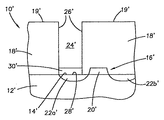
ウエハフラグメント10は、シリコン含有ベース層又は基板12を含むように示される。典型的な基板12は、導電性増強材料で概して軽くドーピングされた単結晶シリコンである。トランジスタ構造16及び被覆絶縁性層18が基板12の表面14に形成されている。ゲート20及び隣接するソース/ドレイン拡散領域22a,22bを含むトランジスタ16は、当該技術で既知であり使用される従来の方法により形成され得る。
絶縁性層18は、単一層又は多層で、酸化物、例えば二酸化シリコン(SiO2)、リンケイ酸ガラス(PSG)、ホウケイ酸ガラス(BSG)及びホウリンケイ酸ガラス(BPSG)を含む。図示された実施の形態ではBPSGである。BPSG絶縁性層18は、絶縁性側壁26及び底部28により規定されたビア又は他のコンタクト開口部24を与えるために、パターニングされたフォトレジスト層(図示せず)でマスクして、既知のフォトリソグラフィー技術、例えば反応性イオンエッチング(RIE)を用いてエッチングされる。コンタクト開口部は、電気的コンタクトが形成される下地シリコン基板12における拡散領域22a(すなわち、ソース/ドレイン領域)に延在する。
The insulating
図1Bを参照して、チタンシリサイド(TiSix)シード層30は、コンタクト開口部24の底部28でシリコン基板の露出表面14上に形成される。通常、シード層は、約250から約300オングストロームの厚さに形成される。拡散領域22aを有する界面で形成された得られたTiSixシード層30は、コンタクト領域における低抵抗のために有用である。チタンシリサイド層を形成する技術及びプロセス系は、当該技術において良く知られており、例えば米国特許第6,086,442号(サンドフ他)及び第5,976,976号(ドア他)に記載されている。
Referring to FIG. 1B, a titanium silicide (TiSix)
好ましくは、TiSixシード層30は、四塩化チタン(TiCl4)、水素(H2)、並びにアルゴン(Ar)及び/又はヘリウム(He)のようなキャリアガスを含むソースガスからRFプラズマを形成することを含む従来のプラズマ励起化学的気相堆積(PECVD)により形成され、基板(シリコン)表面上にチタン(Ti)層を堆積する。チタン膜が堆積されたとき、チタンがシリコンと反応してTiSix膜層30を形成する。TiSixシード層30の配合物を達成するための典型的なプロセス条件は、約600℃のウエハ温度、約0.5から約20Torrのプロセス圧力、約100から約800ワットの電力範囲(平行平板単一ウエハプラズマ反応器を用いる)、並びに約150から約300sccmのTiCl4、約1000から約8000sccmの水素(H2)、約1000sccmのアルゴン(Ar)及び約50sccmの窒素(N2)の流量を含む。
Preferably, the
TiSixシード層を形成する好ましいプロセスはPECVD技術によるが、TiSixシード層30はまた、コンタクト開口部の底部で基板12の表面14上に物理的気相堆積(PVD)、すなわちスパッタリングによりチタンの薄層を堆積し、その後窒素、アルゴン、アンモニア又は水素のような大気ガスにおいてアニールステップ(約650℃)を行うことにより形成され得る。これは、チタンを拡散領域22aの表面14で露出したシリコンと反応させてTiSixシード層30を形成する。そのようなプロセスは、チタン金属がシリコンアクティブ領域に接触するところにのみTiSixが形成されるので、自己整合(self-aligning)と言われる。
Although the preferred process for forming the TiSix seed layer is by PECVD technology, the
TiSixシード層30を堆積する方法の他の例は、従来の低圧CVD(LPCVD)プロセスによるものである。典型的なプロセス条件は、ヘリウムのようなキャリアガス中に約5:1の比で四塩化チタン(TiCl4)とシラン(SiH4)又はジクロロシラン(SiH2Cl2)のようなシリコン前駆物質又はソースガスとを加えたものを用いて、約650℃から約900℃のプロセス温度、及び約10mTorrから約1Torrの圧力を含む。
Another example of a method for depositing the
コンタクト開口部の絶縁性側壁からのコンタクトの剥離及び絶縁性層のクラックのような純粋TiCl4ベース窒化チタンプラグ又はコンタクトの使用において起こる問題を克服するために、本発明は、ボロンドープしたTiCl4ベース窒化チタン充填物(ホウ窒化チタン)を用いて図1Dに示すように導電性コンタクト又はプラグ34を形成する。好ましくは、前述の導電性コンタクトは、従来の熱化学的気相堆積(TCVD)プロセスにより形成される。そのようなTCVD技術及びプロセス系は、当該技術において良く知られており、例えば米国特許第6,037,252号(ヒルマン他)及び第5,908,947号(アイヤー及びシャラン)に記載されている。TCVD系は、コールドウォール/ホットサブストレート反応器及びホットウォール反応器、プラズマ励起反応器、放射ビーム励起反応器などのような標準の熱反応器を含む。 To overcome the problems that occur in the use of pure TiCl 4 based titanium nitride plugs or contacts, such as contact stripping from the insulating sidewalls of the contact openings and cracking of the insulating layer, the present invention provides a boron doped TiCl 4 base. Conductive contacts or plugs 34 are formed using a titanium nitride fill (titanium boronitride) as shown in FIG. 1D. Preferably, the aforementioned conductive contacts are formed by a conventional thermochemical vapor deposition (TCVD) process. Such TCVD techniques and process systems are well known in the art and are described, for example, in US Pat. Nos. 6,037,252 (Hillman et al.) And 5,908,947 (Ayer and Sharan). Yes. TCVD systems include standard thermal reactors such as cold wall / hot substrate reactors and hot wall reactors, plasma excited reactors, radiation beam excited reactors, and the like.
通常、TCVDプロセスにおいて、基板及び/又はガス前駆物質が加熱される反応チャンバ(図示せず)に基板が置かれる。好ましくは、基板は、前駆物質ガスの分解温度を超える温度に加熱される。ガスが反応チャンバに導入され、基板と接触するとき、ガスは基板表面で分解し、金属と前駆物質又は反応ガスの元素(element)とを含むホウ窒化チタン膜を堆積する。 Typically, in a TCVD process, the substrate is placed in a reaction chamber (not shown) in which the substrate and / or gas precursor is heated. Preferably, the substrate is heated to a temperature above the decomposition temperature of the precursor gas. As the gas is introduced into the reaction chamber and contacts the substrate, the gas decomposes at the substrate surface, depositing a titanium boronitride film containing the metal and the precursor or reactive gas elements.
ホット又はコールドウォール熱化学的気相堆積を用いて本発明に係るボロンドープTiN層を堆積する典型的なTCVDプロセスにおいて、ウエハフラグメント10はTCVD反応器(図示せず)内に置かれ、四塩化チタン(TiCl4)、ジボラン(B2H6)、アンモニア(NH3)、並びにアルゴン、ヘリウム及び/又は窒素のような不活性キャリアガスを含むガス材料が、コンタクト開口部24内でチタンシリサイド(TiSix)シード層30上にボロンドープしたTiCl4ベースホウ窒化チタンの層32を化学的気相堆積堆積するために効果的な条件下で反応器に流される。ガス材料は、コンタクト開口部に完全に充填するような厚さに堆積され、図1Cに示す構造になる。ガスの好ましい流量は、TiCl4が約100から500sccm、B2H6が約100から約1000sccm、及びNH3が約100から約1000sccmである。反応器(ホットウォール)内又はサセプタ(コールドウォール)の好ましい温度は、反応器内での圧力条件が約1Torrから約15Torr、好ましくは約10Torrで、約550℃から約700℃、好ましくは約560℃から約650℃の温度である。通常、コンタクト開口部を充填するために、約1000から約3000オングストロームの材料が通常堆積される。
In a typical TCVD process for depositing a boron doped TiN layer according to the present invention using hot or cold wall thermochemical vapor deposition, the
堆積した導電性層32は、一般式TiBxNy(ホウ窒化チタン)を有するTiCl4ベースボロンドープ窒化チタンを含む。その系中に流されるB2H6及びNH3ガスの量は、形成されたコンタクト34が側壁に着いたままになり、側壁から剥がれず、絶縁性層18の本体に実質的なクラックが発生しないような、コンタクト開口部24の絶縁性側壁26への密着レベルを有する充填物を与えるように維持される。
ガス混合物においてB2H6を含めないで作られたTiCl4ベースTiNコンタクトは、コンタクト開口部の絶縁性側壁への密着レベルが低い。これは、結果として開口部の側壁からコンタクトが剥離することになる。さらに、そのようなコンタクトが約200オングストローム又はそれより大きい厚さになると、充填材料の高い熱ストレスが絶縁性層のクラックを引き起こし得る。TiCl4及びNH3ガス成分に対してB2H6の量を増加して添加すると、開口部24の絶縁性側壁26とコンタクト34の充填材料との密着度が向上し、熱ストレスレベルが減少してそれは絶縁性層18のクラックを実質的になくす。しかしながら、ホウ素量が増加するとまた、コンタクト34の導電率レベルが減少(及び抵抗が増加)する。この影響を打ち消すために、拡散エリア22a又は他の半導体構造との効果的な電気的接触のための所定レベルで、形成されたコンタクト34の導電性を維持するために効果的である量で、ガス混合物においてアンモニアが与えられる。
TiCl 4 -based TiN contacts made without B 2 H 6 in the gas mixture have a low level of adhesion to the insulating sidewall of the contact opening. As a result, the contact peels from the side wall of the opening. Furthermore, when such contacts are about 200 angstroms thick or greater, the high thermal stress of the filler material can cause cracking of the insulating layer. When the amount of B 2 H 6 is increased with respect to the TiCl 4 and NH 3 gas components, the adhesion between the insulating
図1Dを参照して、余剰の導電性層32はその後、当該技術において既知の方法、例えば化学的機械的研磨(CMP)により除去されて、半導体デバイスの種々の部分に対して拡散領域(導電性エリア)22aに/から電気的接続を与えるための導電性コンタクト又はプラグ34を形成し得る。
Referring to FIG. 1D, excess
得られたコンタクト34は、コンタクト開口部の底部で基板上に堆積された薄いチタンシリサイド層を覆うボロンドープ窒化チタン層を有する。コンタクト34は、開口部の絶縁性側壁に対する高レベルの密着性を有し、絶縁性層のクラックを実質的になくすような単位面積当たりの力(すなわちGdynes/cm2)で測定される十分に低い熱ストレスレベルを有し、低電気抵抗性で高導電性である。
The resulting
図示しないけれども、パッシベーション層がその後デバイス上に形成され得る。任意に、他の相互接続及びコンタクト構造(図示せず)がその構造を覆って形成され得る。 Although not shown, a passivation layer can then be formed on the device. Optionally, other interconnect and contact structures (not shown) can be formed over the structure.
本発明の方法の他の実施の形態において、図2Aから図2Fに図示するように、多層窒化チタン導電性コンタクトがウエハフラグメントに作られ得る。 In another embodiment of the method of the present invention, a multi-layer titanium nitride conductive contact can be made on the wafer fragment, as illustrated in FIGS. 2A-2F.
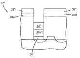
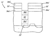
図2Aを参照して、処理前のウエハフラグメント10'が示される。簡単に、ウエハフラグメント10'は、ソース/ドレイン領域のような導電性エリア22a'を有するシリコン含有基板12'、例えば単結晶シリコンを含む。例えばBPSGを含む被覆絶縁層18'は、露出表面19'と、側壁26'及び底部28'を有するコンタクト開口部24'とを有する。コンタクト開口部24'は、導電性エリア22a'に延在する。
Referring to FIG. 2A, a
図2Bを参照して、薄いチタンシリサイド(TiSix)層30'が開口部24'の底部28'で導電性エリア22a'上に形成される。TiSix層30'は、好ましくは約250から約300オングストロームの厚さを有する。TiSix層30'は、前述したように従来の方法により、好ましくはTiCl4、H2及び一つ又はそれ以上のキャリアガスを用いたPECVDにより形成され得る。
Referring to FIG. 2B, a thin titanium silicide (TiSix)
層状導電性コンタクトは、ボロンドープ窒化チタン層が非ドープ窒化チタンの2つの層間に挟まれるように、TiCl4ベース窒化チタンとボロンドープTiCl4ベース窒化チタンとの交互層をコンタクト開口部に堆積することにより形成される。多層コンタクトは、約550℃から約700℃、好ましくは560℃から約650℃の温度で、約1Torから約15Torr、好ましくは10Torrの圧力で従来の熱CVD処理により形成され得る。 Layered conductive contact, as boron-doped titanium nitride layer is sandwiched between two layers of undoped titanium nitride, by depositing alternating layers of the TiCl 4 based on titanium nitride and boron-doped TiCl 4 based titanium nitride in the contact opening It is formed. The multi-layer contact may be formed by conventional thermal CVD processing at a temperature of about 550 ° C. to about 700 ° C., preferably 560 ° C. to about 650 ° C., and a pressure of about 1 Tor to about 15 Torr, preferably 10 Torr.
四塩化チタン(TiCl4)、アンモニア(NH3)及び一つ又はそれ以上のキャリアガスを含むガス混合物が反応器に流され、TiSixシード層30'上に非ドープ窒化チタンの層36a'を所望の厚さ、通常約100から約500オングストロームに形成し得る。得られた構造が図2Cに示される。ガス混合物の好ましい流量は、TiCl4が約100から約500sccm及びNH3が約100から約1000sccmである。
A gas mixture comprising titanium tetrachloride (TiCl 4 ), ammonia (NH 3 ), and one or more carrier gases is flowed into the reactor to provide an undoped
図2Dに示すように、その後ジボラン(B2H6)が反応器に流され、ボロンドープ窒化チタンを含む層32'がTiCl4、NH3及びB2H6を含むガス混合物から非ドープ窒化チタン上に堆積される。ボロンドープ窒化チタン層32'は、約100から約500オングストロームの所望の厚さに堆積される。ガス混合物の好ましい流量は、TiCl4が約100から約500sccm、NH3が約100から約1000sccm、及びB2H6が約100から約1000sccmである。前述したように、NH3及びB2H6の流れは、得られる多層コンタクトの密着性、熱ストレスレベル及び導電性を変更するために制御され得る。
As shown in FIG. 2D, diborane (B 2 H 6 ) is then flowed into the reactor and the
B2H6の流れがその後止められ、第1のガス混合物(すなわちTiCl4、NH3)が反応器内に流されて、図2Eに示すように、非ドープ窒化チタンを含む層36b'が形成される。窒化チタン層36b'は、通常約100から約500オングストロームの所望の厚みに堆積される。窒化チタン層36b'は、開口部を充填するように堆積され得る。あるいは、ボロンドープ窒化チタンのさらなる層が、所望により非ドープ窒化チタンの2つの層間に堆積されて、非ドープ窒化チタンを含む最上層のコンタクトでコンタクト開口部24'を充填し得る。
The flow of B 2 H 6 is then turned off and the first gas mixture (ie, TiCl 4 , NH 3 ) is flowed into the reactor to create a
余剰材料は、図2Fに図示するように、例えばCMPにより除去され、導電性コンタクト34'を形成し得る。
Excess material may be removed, for example, by CMP, as shown in FIG. 2F, to form a
非ドープ窒化チタン間にボロンドープ窒化チタン32'の層を挟むことで、TiCl4ベースTiN充填材料における熱ストレスを実質的に減少する。これは、充填物を導電性コンタクトとして使用させ、高アスペクト比形態におけるタングステン(W)プラグに置き換えさせる。交互層のこの組み合わせは、コンタクト開口部の側壁から、形成されたコンタクトの剥離を実質的になくす密着レベルを有するTiCl4ベースTiNコンタクトを達成する。また、特にコンタクトの厚さが約500オングストローム又はそれより大きくなるとき、絶縁性層の本体のクラックを実質的に減少するより低いレベルの熱ストレスを与える。さらに、得られたコンタクトは、拡散領域又は他の導電性構造に対する効果的な電気的コンタクト用の高い導電性レベルを有する。
By sandwiching a layer of boron-doped
本発明の方法にしたがって、ボロンドープTiCl4ベース窒化チタン(TiN)コンタクトをBPSG層の高アスペクト比開口部に形成した。ジボラン(B2H6)の流れをテスト範囲にわたって変えて、BPSG絶縁性層上のボロンドープTiCl4ベースTiNコンタクトの熱ストレス(Gdynes/cm2)変化をテストした。 In accordance with the method of the present invention, boron doped TiCl 4 based titanium nitride (TiN) contacts were formed in the high aspect ratio openings of the BPSG layer. Diborane (B 2 H 6 ) flow was varied over the test range to test the thermal stress (Gdynes / cm 2 ) change of boron doped TiCl 4 based TiN contacts on the BPSG insulating layer.
シリコン基板層及びBPSGの被覆層を有するウエハフラグメントを与えた。BPSG層を通してコンタクト開口部を形成した。開口部のアスペクト比は10:1であった。 A wafer fragment having a silicon substrate layer and a coating layer of BPSG was provided. A contact opening was formed through the BPSG layer. The aspect ratio of the opening was 10: 1.
カリフォルニア、サンタクララのアプライドマテリアルカンパニーから市販されているセンチュラシステム(Centura system)を用いて10Torrの圧力で熱CVDによりTiCl4ベースTiN膜を堆積した。次のように反応器内に前駆物質ガスを流した:TiCl4を340sccm、NH3を200sccm、アルゴン(Ar)を3000sccm、ガス状窒素(N2)を2000sccm。200sccmから600sccmの範囲の流量で反応器内にジボラン(B2H6)を流した。2つの異なる温度600℃及び650℃でデータを測定した。
TiCl 4 -based TiN films were deposited by thermal CVD at a pressure of 10 Torr using a Centura system commercially available from the Applied Materials Company of Santa Clara, California. The precursor gas was flowed into the reactor as follows: TiCl 4 340 sccm,
その結果をグラフの形で図3A及び図3Bに示す。それらに示されるように、ボロン(すなわちB2H6)の量が増加するにつれて、TiCl4ベースTiN材料のストレス(Gdynes/cm2)が中間の又はゼロのストレスレベル及びそれより下に減少する。したがって、B2H6流を変えることにより、材料が絶縁性層(例えばBPSG)をクラックさせないようにTiCl4ベースTiN膜の熱ストレスを調整することができる。 The results are shown in graph form in FIGS. 3A and 3B. As shown, as the amount of boron (ie B 2 H 6 ) increases, the stress (Gdynes / cm 2 ) of the TiCl 4 based TiN material decreases to medium or zero stress levels and below. . Thus, by varying the B 2 H 6 flow can material to adjust the thermal stress of TiCl 4 base TiN film so as not to crack the insulation layer (e.g., BPSG).
法令にしたがって、本発明は、構造的及び方法的形態に関して大体の仕様を言葉で説明している。しかしながら、ここで開示された手段は本発明を効果に至らしめる好ましい形を含むので、本発明が示され記載された特定の形態に限定されないことに留意すべきである。したがって、本発明は、均等論にしたがって適切に解釈された添付請求項の適正な範囲内でその形又は変形例のすべてで請求される。 In accordance with the statute, the present invention verbally describes the general specifications with regard to structural and methodological forms. It should be noted, however, that the means disclosed herein are not limited to the specific forms shown and described, as they include preferred forms that effect the invention. Therefore, the invention is claimed in all its forms or variations within the proper scope of the appended claims properly interpreted according to the doctrine of equivalents.
Claims (16)
前記開口部内における前記基板上にチタンシリサイド層を形成することと、
前記チタンシリサイド層上にホウ窒化チタンを含む充填物を形成して、前記開口部を充填することと
を有する方法。A method of forming a conductive contact in the opening in the insulating layer exists on the substrate,
Forming a Chitanshirisai de layer on the substrate within the opening,
Wherein forming a filling containing boric titanium nitride over the titanium silicide layer, a method and a filling said opening.
合物、ならびにジボランを含まない、四塩化チタン及びアンモニアを含むガス混合物を用いる化学気相堆積を含む、請求項5に記載の方法。 Wherein forming the packings, titanium tetrachloride, ammonia, and gas mixtures containing diborane, and does not include diborane, including chemical vapor deposition using a gas mixture containing titanium tetrachloride and ammonia, to claim 5 The method described.
Applications Claiming Priority (2)
| Application Number | Priority Date | Filing Date | Title |
|---|---|---|---|
| US09/918,919 US6696368B2 (en) | 2001-07-31 | 2001-07-31 | Titanium boronitride layer for high aspect ratio semiconductor devices |
| PCT/US2002/024088 WO2003012860A2 (en) | 2001-07-31 | 2002-07-30 | Boron-doped titanium nitride layer for high aspect ratio semiconductor devices |
Publications (3)
| Publication Number | Publication Date |
|---|---|
| JP2005527098A JP2005527098A (en) | 2005-09-08 |
| JP2005527098A5 JP2005527098A5 (en) | 2006-01-05 |
| JP4168397B2 true JP4168397B2 (en) | 2008-10-22 |
Family
ID=25441171
Family Applications (1)
| Application Number | Title | Priority Date | Filing Date |
|---|---|---|---|
| JP2003517937A Expired - Lifetime JP4168397B2 (en) | 2001-07-31 | 2002-07-30 | Boron doped titanium nitride layer for high aspect ratio semiconductor devices |
Country Status (7)
| Country | Link |
|---|---|
| US (2) | US6696368B2 (en) |
| EP (1) | EP1412976B1 (en) |
| JP (1) | JP4168397B2 (en) |
| KR (1) | KR100715389B1 (en) |
| CN (1) | CN100352035C (en) |
| AT (1) | ATE532212T1 (en) |
| WO (1) | WO2003012860A2 (en) |
Families Citing this family (17)
| Publication number | Priority date | Publication date | Assignee | Title |
|---|---|---|---|---|
| US20030036242A1 (en) * | 2001-08-16 | 2003-02-20 | Haining Yang | Methods of forming metal-comprising materials and capacitor electrodes; and capacitor constructions |
| US6746952B2 (en) * | 2001-08-29 | 2004-06-08 | Micron Technology, Inc. | Diffusion barrier layer for semiconductor wafer fabrication |
| US7067416B2 (en) | 2001-08-29 | 2006-06-27 | Micron Technology, Inc. | Method of forming a conductive contact |
| US7164165B2 (en) * | 2002-05-16 | 2007-01-16 | Micron Technology, Inc. | MIS capacitor |
| US7150789B2 (en) * | 2002-07-29 | 2006-12-19 | Micron Technology, Inc. | Atomic layer deposition methods |
| US6890596B2 (en) * | 2002-08-15 | 2005-05-10 | Micron Technology, Inc. | Deposition methods |
| US6753271B2 (en) * | 2002-08-15 | 2004-06-22 | Micron Technology, Inc. | Atomic layer deposition methods |
| US6673701B1 (en) * | 2002-08-27 | 2004-01-06 | Micron Technology, Inc. | Atomic layer deposition methods |
| KR100487563B1 (en) * | 2003-04-30 | 2005-05-03 | 삼성전자주식회사 | Semiconductor device and method of forming the same |
| US7233073B2 (en) * | 2003-07-31 | 2007-06-19 | Matsushita Electric Industrial Co., Ltd. | Semiconductor device and method for fabricating the same |
| US7358172B2 (en) * | 2006-02-21 | 2008-04-15 | International Business Machines Corporation | Poly filled substrate contact on SOI structure |
| CN103022163A (en) * | 2011-09-22 | 2013-04-03 | 比亚迪股份有限公司 | Crystal silicon solar cell and preparation method thereof |
| EP3032575B1 (en) * | 2014-12-08 | 2020-10-21 | IMEC vzw | Method for forming an electrical contact. |
| US10854505B2 (en) | 2016-03-24 | 2020-12-01 | Taiwan Semiconductor Manufacturing Company, Ltd. | Removing polymer through treatment |
| US10355139B2 (en) | 2016-06-28 | 2019-07-16 | Sandisk Technologies Llc | Three-dimensional memory device with amorphous barrier layer and method of making thereof |
| US10361213B2 (en) * | 2016-06-28 | 2019-07-23 | Sandisk Technologies Llc | Three dimensional memory device containing multilayer wordline barrier films and method of making thereof |
| US20180331118A1 (en) | 2017-05-12 | 2018-11-15 | Sandisk Technologies Llc | Multi-layer barrier for cmos under array type memory device and method of making thereof |
Family Cites Families (21)
| Publication number | Priority date | Publication date | Assignee | Title |
|---|---|---|---|---|
| JPH05267220A (en) | 1992-03-19 | 1993-10-15 | Sony Corp | Adhesion layer for semiconductor device and method for forming metal plug |
| US5747116A (en) | 1994-11-08 | 1998-05-05 | Micron Technology, Inc. | Method of forming an electrical contact to a silicon substrate |
| US5946594A (en) | 1996-01-02 | 1999-08-31 | Micron Technology, Inc. | Chemical vapor deposition of titanium from titanium tetrachloride and hydrocarbon reactants |
| FR2744461B1 (en) * | 1996-02-01 | 1998-05-22 | Tecmachine | TITANIUM NITRIDE DOPED BY BORON, SUBSTRATE COATING BASED ON THIS NEW COMPOUND, HAVING HIGH HARDNESS AND ALLOWING VERY GOOD WEAR RESISTANCE, AND PARTS WITH SUCH COATING |
| US5908947A (en) | 1996-02-09 | 1999-06-01 | Micron Technology, Inc. | Difunctional amino precursors for the deposition of films comprising metals |
| US5990021A (en) | 1997-12-19 | 1999-11-23 | Micron Technology, Inc. | Integrated circuit having self-aligned CVD-tungsten/titanium contact plugs strapped with metal interconnect and method of manufacture |
| US5700716A (en) | 1996-02-23 | 1997-12-23 | Micron Technology, Inc. | Method for forming low contact resistance contacts, vias, and plugs with diffusion barriers |
| JPH09306870A (en) | 1996-05-15 | 1997-11-28 | Nec Corp | Forming barrier film |
| US5977636A (en) | 1997-01-17 | 1999-11-02 | Micron Technology, Inc. | Method of forming an electrically conductive contact plug, method of forming a reactive or diffusion barrier layer over a substrate, integrated circuitry, and method of forming a layer of titanium boride |
| US5976976A (en) | 1997-08-21 | 1999-11-02 | Micron Technology, Inc. | Method of forming titanium silicide and titanium by chemical vapor deposition |
| US5856237A (en) * | 1997-10-20 | 1999-01-05 | Industrial Technology Research Institute | Insitu formation of TiSi2/TiN bi-layer structures using self-aligned nitridation treatment on underlying CVD-TiSi2 layer |
| US6037252A (en) | 1997-11-05 | 2000-03-14 | Tokyo Electron Limited | Method of titanium nitride contact plug formation |
| US6156638A (en) | 1998-04-10 | 2000-12-05 | Micron Technology, Inc. | Integrated circuitry and method of restricting diffusion from one material to another |
| KR100331261B1 (en) * | 1998-12-30 | 2002-08-22 | 주식회사 하이닉스반도체 | Manufacturing Method of Semiconductor Device |
| US6086442A (en) | 1999-03-01 | 2000-07-11 | Micron Technology, Inc. | Method of forming field emission devices |
| US6329670B1 (en) | 1999-04-06 | 2001-12-11 | Micron Technology, Inc. | Conductive material for integrated circuit fabrication |
| US6200649B1 (en) * | 1999-07-21 | 2001-03-13 | Southwest Research Institute | Method of making titanium boronitride coatings using ion beam assisted deposition |
| US6635939B2 (en) * | 1999-08-24 | 2003-10-21 | Micron Technology, Inc. | Boron incorporated diffusion barrier material |
| DE10019164A1 (en) | 2000-04-12 | 2001-10-18 | Mannesmann Ag | SIM lock on certain IMSI areas of a SIM card for prepaid and postpaid cards |
| US7067416B2 (en) * | 2001-08-29 | 2006-06-27 | Micron Technology, Inc. | Method of forming a conductive contact |
| US6746952B2 (en) * | 2001-08-29 | 2004-06-08 | Micron Technology, Inc. | Diffusion barrier layer for semiconductor wafer fabrication |
-
2001
- 2001-07-31 US US09/918,919 patent/US6696368B2/en not_active Expired - Lifetime
-
2002
- 2002-07-30 KR KR1020047001585A patent/KR100715389B1/en not_active Expired - Lifetime
- 2002-07-30 AT AT02765900T patent/ATE532212T1/en active
- 2002-07-30 EP EP02765900A patent/EP1412976B1/en not_active Expired - Lifetime
- 2002-07-30 WO PCT/US2002/024088 patent/WO2003012860A2/en not_active Ceased
- 2002-07-30 CN CNB028152131A patent/CN100352035C/en not_active Expired - Lifetime
- 2002-07-30 JP JP2003517937A patent/JP4168397B2/en not_active Expired - Lifetime
- 2002-11-04 US US10/287,203 patent/US6822299B2/en not_active Expired - Lifetime
Also Published As
| Publication number | Publication date |
|---|---|
| KR100715389B1 (en) | 2007-05-08 |
| WO2003012860A3 (en) | 2003-11-27 |
| US6822299B2 (en) | 2004-11-23 |
| JP2005527098A (en) | 2005-09-08 |
| US20030025206A1 (en) | 2003-02-06 |
| US20030075802A1 (en) | 2003-04-24 |
| ATE532212T1 (en) | 2011-11-15 |
| US6696368B2 (en) | 2004-02-24 |
| CN100352035C (en) | 2007-11-28 |
| EP1412976B1 (en) | 2011-11-02 |
| KR20040019102A (en) | 2004-03-04 |
| CN1539164A (en) | 2004-10-20 |
| EP1412976A2 (en) | 2004-04-28 |
| WO2003012860A2 (en) | 2003-02-13 |
Similar Documents
| Publication | Publication Date | Title |
|---|---|---|
| KR100546943B1 (en) | Semiconductor Device Formation Method | |
| US6940172B2 (en) | Chemical vapor deposition of titanium | |
| US6171943B1 (en) | Methods of forming a contact having titanium silicide formed by chemical vapor deposition | |
| JP4168397B2 (en) | Boron doped titanium nitride layer for high aspect ratio semiconductor devices | |
| US6888252B2 (en) | Method of forming a conductive contact | |
| US6746952B2 (en) | Diffusion barrier layer for semiconductor wafer fabrication | |
| US5977636A (en) | Method of forming an electrically conductive contact plug, method of forming a reactive or diffusion barrier layer over a substrate, integrated circuitry, and method of forming a layer of titanium boride | |
| US6245674B1 (en) | Method of forming a metal silicide comprising contact over a substrate | |
| US6433434B1 (en) | Apparatus having a titanium alloy layer | |
| KR100543653B1 (en) | Metal wiring formation method of semiconductor device | |
| KR100607756B1 (en) | Tungsten contact electrode manufacturing method of semiconductor device | |
| KR20060058583A (en) | Conductive structure, manufacturing method thereof, semiconductor device including same and manufacturing method thereof | |
| KR100406562B1 (en) | Method for forming metal line | |
| KR20050002094A (en) | Method for forming a metal line in semiconductor device |
Legal Events
| Date | Code | Title | Description |
|---|---|---|---|
| A521 | Request for written amendment filed |
Free format text: JAPANESE INTERMEDIATE CODE: A523 Effective date: 20050729 |
|
| A621 | Written request for application examination |
Free format text: JAPANESE INTERMEDIATE CODE: A621 Effective date: 20050729 |
|
| A977 | Report on retrieval |
Free format text: JAPANESE INTERMEDIATE CODE: A971007 Effective date: 20070403 |
|
| A521 | Request for written amendment filed |
Free format text: JAPANESE INTERMEDIATE CODE: A821 Effective date: 20071004 |
|
| RD02 | Notification of acceptance of power of attorney |
Free format text: JAPANESE INTERMEDIATE CODE: A7422 Effective date: 20071004 |
|
| RD04 | Notification of resignation of power of attorney |
Free format text: JAPANESE INTERMEDIATE CODE: A7424 Effective date: 20071005 |
|
| A131 | Notification of reasons for refusal |
Free format text: JAPANESE INTERMEDIATE CODE: A131 Effective date: 20080325 |
|
| A521 | Request for written amendment filed |
Free format text: JAPANESE INTERMEDIATE CODE: A821 Effective date: 20080617 Free format text: JAPANESE INTERMEDIATE CODE: A523 Effective date: 20080617 |
|
| TRDD | Decision of grant or rejection written | ||
| A01 | Written decision to grant a patent or to grant a registration (utility model) |
Free format text: JAPANESE INTERMEDIATE CODE: A01 Effective date: 20080715 |
|
| A01 | Written decision to grant a patent or to grant a registration (utility model) |
Free format text: JAPANESE INTERMEDIATE CODE: A01 |
|
| A61 | First payment of annual fees (during grant procedure) |
Free format text: JAPANESE INTERMEDIATE CODE: A61 Effective date: 20080724 |
|
| FPAY | Renewal fee payment (event date is renewal date of database) |
Free format text: PAYMENT UNTIL: 20110815 Year of fee payment: 3 |
|
| R150 | Certificate of patent or registration of utility model |
Ref document number: 4168397 Country of ref document: JP Free format text: JAPANESE INTERMEDIATE CODE: R150 Free format text: JAPANESE INTERMEDIATE CODE: R150 |
|
| FPAY | Renewal fee payment (event date is renewal date of database) |
Free format text: PAYMENT UNTIL: 20110815 Year of fee payment: 3 |
|
| FPAY | Renewal fee payment (event date is renewal date of database) |
Free format text: PAYMENT UNTIL: 20120815 Year of fee payment: 4 |
|
| R250 | Receipt of annual fees |
Free format text: JAPANESE INTERMEDIATE CODE: R250 |
|
| FPAY | Renewal fee payment (event date is renewal date of database) |
Free format text: PAYMENT UNTIL: 20130815 Year of fee payment: 5 |
|
| R250 | Receipt of annual fees |
Free format text: JAPANESE INTERMEDIATE CODE: R250 |
|
| R250 | Receipt of annual fees |
Free format text: JAPANESE INTERMEDIATE CODE: R250 |
|
| R250 | Receipt of annual fees |
Free format text: JAPANESE INTERMEDIATE CODE: R250 |
|
| R250 | Receipt of annual fees |
Free format text: JAPANESE INTERMEDIATE CODE: R250 |
|
| R250 | Receipt of annual fees |
Free format text: JAPANESE INTERMEDIATE CODE: R250 |
|
| R250 | Receipt of annual fees |
Free format text: JAPANESE INTERMEDIATE CODE: R250 |
|
| R250 | Receipt of annual fees |
Free format text: JAPANESE INTERMEDIATE CODE: R250 |
|
| R250 | Receipt of annual fees |
Free format text: JAPANESE INTERMEDIATE CODE: R250 |
|
| R250 | Receipt of annual fees |
Free format text: JAPANESE INTERMEDIATE CODE: R250 |
|
| R250 | Receipt of annual fees |
Free format text: JAPANESE INTERMEDIATE CODE: R250 |
|
| EXPY | Cancellation because of completion of term |