JP4159288B2 - Imaging system including a detector framing node - Google Patents
Imaging system including a detector framing node Download PDFInfo
- Publication number
- JP4159288B2 JP4159288B2 JP2002001008A JP2002001008A JP4159288B2 JP 4159288 B2 JP4159288 B2 JP 4159288B2 JP 2002001008 A JP2002001008 A JP 2002001008A JP 2002001008 A JP2002001008 A JP 2002001008A JP 4159288 B2 JP4159288 B2 JP 4159288B2
- Authority
- JP
- Japan
- Prior art keywords
- dfn
- event
- image
- data
- bus
- Prior art date
- Legal status (The legal status is an assumption and is not a legal conclusion. Google has not performed a legal analysis and makes no representation as to the accuracy of the status listed.)
- Expired - Fee Related
Links
- 238000009432 framing Methods 0.000 title claims description 106
- 238000003384 imaging method Methods 0.000 title description 64
- 239000000872 buffer Substances 0.000 claims description 250
- 230000015654 memory Effects 0.000 claims description 244
- 238000001514 detection method Methods 0.000 claims description 162
- 230000006854 communication Effects 0.000 claims description 154
- 238000004891 communication Methods 0.000 claims description 154
- 230000004044 response Effects 0.000 claims description 123
- 239000000835 fiber Substances 0.000 claims description 89
- 230000005855 radiation Effects 0.000 claims description 64
- 230000005540 biological transmission Effects 0.000 claims description 34
- 239000013307 optical fiber Substances 0.000 claims description 34
- 229910021417 amorphous silicon Inorganic materials 0.000 claims description 26
- 238000012360 testing method Methods 0.000 description 126
- 238000010586 diagram Methods 0.000 description 116
- 230000006870 function Effects 0.000 description 63
- 238000000034 method Methods 0.000 description 60
- 230000000747 cardiac effect Effects 0.000 description 45
- 238000012546 transfer Methods 0.000 description 42
- 238000009607 mammography Methods 0.000 description 40
- 238000012545 processing Methods 0.000 description 39
- 230000008569 process Effects 0.000 description 33
- 238000013515 script Methods 0.000 description 29
- 238000004883 computer application Methods 0.000 description 20
- 238000012937 correction Methods 0.000 description 20
- 230000008859 change Effects 0.000 description 17
- 230000007704 transition Effects 0.000 description 14
- 238000013461 design Methods 0.000 description 12
- 238000002594 fluoroscopy Methods 0.000 description 12
- 238000012544 monitoring process Methods 0.000 description 12
- 230000008707 rearrangement Effects 0.000 description 12
- 230000003287 optical effect Effects 0.000 description 11
- 230000008439 repair process Effects 0.000 description 10
- 230000002950 deficient Effects 0.000 description 9
- 238000007726 management method Methods 0.000 description 9
- 238000003860 storage Methods 0.000 description 9
- 238000005516 engineering process Methods 0.000 description 8
- 230000005669 field effect Effects 0.000 description 8
- 238000004519 manufacturing process Methods 0.000 description 7
- 238000013507 mapping Methods 0.000 description 7
- 230000001960 triggered effect Effects 0.000 description 7
- 238000004422 calculation algorithm Methods 0.000 description 6
- 239000013078 crystal Substances 0.000 description 6
- 239000010408 film Substances 0.000 description 6
- OAICVXFJPJFONN-UHFFFAOYSA-N Phosphorus Chemical compound [P] OAICVXFJPJFONN-UHFFFAOYSA-N 0.000 description 5
- 230000002159 abnormal effect Effects 0.000 description 5
- 239000008186 active pharmaceutical agent Substances 0.000 description 5
- 239000003990 capacitor Substances 0.000 description 5
- 238000006243 chemical reaction Methods 0.000 description 5
- 230000008878 coupling Effects 0.000 description 5
- 238000010168 coupling process Methods 0.000 description 5
- 238000005859 coupling reaction Methods 0.000 description 5
- 238000002059 diagnostic imaging Methods 0.000 description 5
- 230000000694 effects Effects 0.000 description 5
- 239000011521 glass Substances 0.000 description 5
- 230000010354 integration Effects 0.000 description 5
- 230000001360 synchronised effect Effects 0.000 description 5
- 230000003139 buffering effect Effects 0.000 description 4
- 210000004027 cell Anatomy 0.000 description 4
- 229910052751 metal Inorganic materials 0.000 description 4
- 239000002184 metal Substances 0.000 description 4
- 229910021421 monocrystalline silicon Inorganic materials 0.000 description 4
- 239000002245 particle Substances 0.000 description 4
- 238000012805 post-processing Methods 0.000 description 4
- 102100036409 Activated CDC42 kinase 1 Human genes 0.000 description 3
- 102100031941 Enhancer of polycomb homolog 2 Human genes 0.000 description 3
- 101000928956 Homo sapiens Activated CDC42 kinase 1 Proteins 0.000 description 3
- 101000920664 Homo sapiens Enhancer of polycomb homolog 2 Proteins 0.000 description 3
- 238000010521 absorption reaction Methods 0.000 description 3
- 230000009471 action Effects 0.000 description 3
- 230000007175 bidirectional communication Effects 0.000 description 3
- 238000004364 calculation method Methods 0.000 description 3
- 230000007547 defect Effects 0.000 description 3
- 230000001934 delay Effects 0.000 description 3
- 238000011161 development Methods 0.000 description 3
- 230000018109 developmental process Effects 0.000 description 3
- 230000005670 electromagnetic radiation Effects 0.000 description 3
- 239000000463 material Substances 0.000 description 3
- 210000004940 nucleus Anatomy 0.000 description 3
- 238000002360 preparation method Methods 0.000 description 3
- 238000002601 radiography Methods 0.000 description 3
- 230000008672 reprogramming Effects 0.000 description 3
- 239000000523 sample Substances 0.000 description 3
- 239000007787 solid Substances 0.000 description 3
- 230000003068 static effect Effects 0.000 description 3
- 239000000758 substrate Substances 0.000 description 3
- 229910052715 tantalum Inorganic materials 0.000 description 3
- GUVRBAGPIYLISA-UHFFFAOYSA-N tantalum atom Chemical compound [Ta] GUVRBAGPIYLISA-UHFFFAOYSA-N 0.000 description 3
- 230000000007 visual effect Effects 0.000 description 3
- 101100288236 Arabidopsis thaliana KRP4 gene Proteins 0.000 description 2
- 101100433979 Bos taurus TNK2 gene Proteins 0.000 description 2
- 101150002258 HDR1 gene Proteins 0.000 description 2
- 101100385394 Zea mays ACK2 gene Proteins 0.000 description 2
- 230000008901 benefit Effects 0.000 description 2
- 230000002457 bidirectional effect Effects 0.000 description 2
- 230000015572 biosynthetic process Effects 0.000 description 2
- XQPRBTXUXXVTKB-UHFFFAOYSA-M caesium iodide Chemical compound [I-].[Cs+] XQPRBTXUXXVTKB-UHFFFAOYSA-M 0.000 description 2
- 238000013500 data storage Methods 0.000 description 2
- 201000010099 disease Diseases 0.000 description 2
- 208000037265 diseases, disorders, signs and symptoms Diseases 0.000 description 2
- 238000009826 distribution Methods 0.000 description 2
- 230000001976 improved effect Effects 0.000 description 2
- 230000006872 improvement Effects 0.000 description 2
- 230000000977 initiatory effect Effects 0.000 description 2
- 238000007689 inspection Methods 0.000 description 2
- 230000003993 interaction Effects 0.000 description 2
- PWPJGUXAGUPAHP-UHFFFAOYSA-N lufenuron Chemical compound C1=C(Cl)C(OC(F)(F)C(C(F)(F)F)F)=CC(Cl)=C1NC(=O)NC(=O)C1=C(F)C=CC=C1F PWPJGUXAGUPAHP-UHFFFAOYSA-N 0.000 description 2
- 238000002595 magnetic resonance imaging Methods 0.000 description 2
- 230000007246 mechanism Effects 0.000 description 2
- 238000012986 modification Methods 0.000 description 2
- 230000004048 modification Effects 0.000 description 2
- 230000002093 peripheral effect Effects 0.000 description 2
- 238000000623 plasma-assisted chemical vapour deposition Methods 0.000 description 2
- 238000007781 pre-processing Methods 0.000 description 2
- 238000007639 printing Methods 0.000 description 2
- 230000000644 propagated effect Effects 0.000 description 2
- 238000012887 quadratic function Methods 0.000 description 2
- 230000002829 reductive effect Effects 0.000 description 2
- 230000003252 repetitive effect Effects 0.000 description 2
- 238000004088 simulation Methods 0.000 description 2
- 208000010392 Bone Fractures Diseases 0.000 description 1
- XUIMIQQOPSSXEZ-UHFFFAOYSA-N Silicon Chemical compound [Si] XUIMIQQOPSSXEZ-UHFFFAOYSA-N 0.000 description 1
- MCVAAHQLXUXWLC-UHFFFAOYSA-N [O-2].[O-2].[S-2].[Gd+3].[Gd+3] Chemical compound [O-2].[O-2].[S-2].[Gd+3].[Gd+3] MCVAAHQLXUXWLC-UHFFFAOYSA-N 0.000 description 1
- 230000005856 abnormality Effects 0.000 description 1
- 230000003213 activating effect Effects 0.000 description 1
- 230000004913 activation Effects 0.000 description 1
- 238000004458 analytical method Methods 0.000 description 1
- -1 and in particular Inorganic materials 0.000 description 1
- 238000013459 approach Methods 0.000 description 1
- 238000003491 array Methods 0.000 description 1
- 210000000481 breast Anatomy 0.000 description 1
- 230000015556 catabolic process Effects 0.000 description 1
- 210000003855 cell nucleus Anatomy 0.000 description 1
- 210000000038 chest Anatomy 0.000 description 1
- 238000011976 chest X-ray Methods 0.000 description 1
- 239000011248 coating agent Substances 0.000 description 1
- 238000000576 coating method Methods 0.000 description 1
- 238000002591 computed tomography Methods 0.000 description 1
- 238000004590 computer program Methods 0.000 description 1
- 238000001816 cooling Methods 0.000 description 1
- 125000004122 cyclic group Chemical group 0.000 description 1
- 238000013523 data management Methods 0.000 description 1
- 238000006731 degradation reaction Methods 0.000 description 1
- 230000000593 degrading effect Effects 0.000 description 1
- 230000003111 delayed effect Effects 0.000 description 1
- 230000001066 destructive effect Effects 0.000 description 1
- 238000002405 diagnostic procedure Methods 0.000 description 1
- 230000005686 electrostatic field Effects 0.000 description 1
- 239000010437 gem Substances 0.000 description 1
- 210000005260 human cell Anatomy 0.000 description 1
- 235000003642 hunger Nutrition 0.000 description 1
- 239000012535 impurity Substances 0.000 description 1
- 238000010348 incorporation Methods 0.000 description 1
- 239000012212 insulator Substances 0.000 description 1
- 238000002697 interventional radiology Methods 0.000 description 1
- 238000012423 maintenance Methods 0.000 description 1
- 239000011159 matrix material Substances 0.000 description 1
- 230000005499 meniscus Effects 0.000 description 1
- 150000002739 metals Chemical class 0.000 description 1
- 239000000203 mixture Substances 0.000 description 1
- 238000012806 monitoring device Methods 0.000 description 1
- 238000009206 nuclear medicine Methods 0.000 description 1
- 238000004091 panning Methods 0.000 description 1
- 230000036961 partial effect Effects 0.000 description 1
- 230000001575 pathological effect Effects 0.000 description 1
- 230000000149 penetrating effect Effects 0.000 description 1
- 238000003825 pressing Methods 0.000 description 1
- 238000011112 process operation Methods 0.000 description 1
- 238000003672 processing method Methods 0.000 description 1
- 230000001681 protective effect Effects 0.000 description 1
- 230000002285 radioactive effect Effects 0.000 description 1
- 238000001454 recorded image Methods 0.000 description 1
- 230000002441 reversible effect Effects 0.000 description 1
- 238000012552 review Methods 0.000 description 1
- 230000000630 rising effect Effects 0.000 description 1
- 238000012216 screening Methods 0.000 description 1
- 239000004065 semiconductor Substances 0.000 description 1
- 238000007493 shaping process Methods 0.000 description 1
- 230000007781 signaling event Effects 0.000 description 1
- 229910052710 silicon Inorganic materials 0.000 description 1
- 239000010703 silicon Substances 0.000 description 1
- 229910000679 solder Inorganic materials 0.000 description 1
- 238000005476 soldering Methods 0.000 description 1
- 230000007480 spreading Effects 0.000 description 1
- 238000003892 spreading Methods 0.000 description 1
- 238000004544 sputter deposition Methods 0.000 description 1
- 230000037351 starvation Effects 0.000 description 1
- 239000000126 substance Substances 0.000 description 1
- 238000001356 surgical procedure Methods 0.000 description 1
- 230000026676 system process Effects 0.000 description 1
- 238000002560 therapeutic procedure Methods 0.000 description 1
- 239000010409 thin film Substances 0.000 description 1
- 210000001519 tissue Anatomy 0.000 description 1
- 238000003325 tomography Methods 0.000 description 1
- 230000001052 transient effect Effects 0.000 description 1
- 238000000411 transmission spectrum Methods 0.000 description 1
- 201000008827 tuberculosis Diseases 0.000 description 1
- 238000012800 visualization Methods 0.000 description 1
- 238000004876 x-ray fluorescence Methods 0.000 description 1
Images


Classifications
-
- A—HUMAN NECESSITIES
- A61—MEDICAL OR VETERINARY SCIENCE; HYGIENE
- A61B—DIAGNOSIS; SURGERY; IDENTIFICATION
- A61B6/00—Apparatus or devices for radiation diagnosis; Apparatus or devices for radiation diagnosis combined with radiation therapy equipment
- A61B6/42—Arrangements for detecting radiation specially adapted for radiation diagnosis
- A61B6/4208—Arrangements for detecting radiation specially adapted for radiation diagnosis characterised by using a particular type of detector
- A61B6/4233—Arrangements for detecting radiation specially adapted for radiation diagnosis characterised by using a particular type of detector using matrix detectors
-
- A—HUMAN NECESSITIES
- A61—MEDICAL OR VETERINARY SCIENCE; HYGIENE
- A61B—DIAGNOSIS; SURGERY; IDENTIFICATION
- A61B6/00—Apparatus or devices for radiation diagnosis; Apparatus or devices for radiation diagnosis combined with radiation therapy equipment
- A61B6/44—Constructional features of apparatus for radiation diagnosis
- A61B6/4417—Constructional features of apparatus for radiation diagnosis related to combined acquisition of different diagnostic modalities
-
- A—HUMAN NECESSITIES
- A61—MEDICAL OR VETERINARY SCIENCE; HYGIENE
- A61B—DIAGNOSIS; SURGERY; IDENTIFICATION
- A61B6/00—Apparatus or devices for radiation diagnosis; Apparatus or devices for radiation diagnosis combined with radiation therapy equipment
- A61B6/48—Diagnostic techniques
- A61B6/486—Diagnostic techniques involving generating temporal series of image data
- A61B6/487—Diagnostic techniques involving generating temporal series of image data involving fluoroscopy
-
- G—PHYSICS
- G16—INFORMATION AND COMMUNICATION TECHNOLOGY [ICT] SPECIALLY ADAPTED FOR SPECIFIC APPLICATION FIELDS
- G16H—HEALTHCARE INFORMATICS, i.e. INFORMATION AND COMMUNICATION TECHNOLOGY [ICT] SPECIALLY ADAPTED FOR THE HANDLING OR PROCESSING OF MEDICAL OR HEALTHCARE DATA
- G16H30/00—ICT specially adapted for the handling or processing of medical images
- G16H30/20—ICT specially adapted for the handling or processing of medical images for handling medical images, e.g. DICOM, HL7 or PACS
-
- G—PHYSICS
- G16—INFORMATION AND COMMUNICATION TECHNOLOGY [ICT] SPECIALLY ADAPTED FOR SPECIFIC APPLICATION FIELDS
- G16H—HEALTHCARE INFORMATICS, i.e. INFORMATION AND COMMUNICATION TECHNOLOGY [ICT] SPECIALLY ADAPTED FOR THE HANDLING OR PROCESSING OF MEDICAL OR HEALTHCARE DATA
- G16H30/00—ICT specially adapted for the handling or processing of medical images
- G16H30/40—ICT specially adapted for the handling or processing of medical images for processing medical images, e.g. editing
-
- G—PHYSICS
- G16—INFORMATION AND COMMUNICATION TECHNOLOGY [ICT] SPECIALLY ADAPTED FOR SPECIFIC APPLICATION FIELDS
- G16H—HEALTHCARE INFORMATICS, i.e. INFORMATION AND COMMUNICATION TECHNOLOGY [ICT] SPECIALLY ADAPTED FOR THE HANDLING OR PROCESSING OF MEDICAL OR HEALTHCARE DATA
- G16H40/00—ICT specially adapted for the management or administration of healthcare resources or facilities; ICT specially adapted for the management or operation of medical equipment or devices
- G16H40/60—ICT specially adapted for the management or administration of healthcare resources or facilities; ICT specially adapted for the management or operation of medical equipment or devices for the operation of medical equipment or devices
- G16H40/63—ICT specially adapted for the management or administration of healthcare resources or facilities; ICT specially adapted for the management or operation of medical equipment or devices for the operation of medical equipment or devices for local operation
-
- A—HUMAN NECESSITIES
- A61—MEDICAL OR VETERINARY SCIENCE; HYGIENE
- A61B—DIAGNOSIS; SURGERY; IDENTIFICATION
- A61B6/00—Apparatus or devices for radiation diagnosis; Apparatus or devices for radiation diagnosis combined with radiation therapy equipment
- A61B6/50—Apparatus or devices for radiation diagnosis; Apparatus or devices for radiation diagnosis combined with radiation therapy equipment specially adapted for specific body parts; specially adapted for specific clinical applications
- A61B6/502—Apparatus or devices for radiation diagnosis; Apparatus or devices for radiation diagnosis combined with radiation therapy equipment specially adapted for specific body parts; specially adapted for specific clinical applications for diagnosis of breast, i.e. mammography
-
- H—ELECTRICITY
- H04—ELECTRIC COMMUNICATION TECHNIQUE
- H04N—PICTORIAL COMMUNICATION, e.g. TELEVISION
- H04N5/00—Details of television systems
- H04N5/30—Transforming light or analogous information into electric information
- H04N5/32—Transforming X-rays
Landscapes
- Health & Medical Sciences (AREA)
- Engineering & Computer Science (AREA)
- Life Sciences & Earth Sciences (AREA)
- Medical Informatics (AREA)
- Public Health (AREA)
- General Health & Medical Sciences (AREA)
- Radiology & Medical Imaging (AREA)
- Nuclear Medicine, Radiotherapy & Molecular Imaging (AREA)
- Biomedical Technology (AREA)
- Physics & Mathematics (AREA)
- Molecular Biology (AREA)
- Veterinary Medicine (AREA)
- Optics & Photonics (AREA)
- Heart & Thoracic Surgery (AREA)
- High Energy & Nuclear Physics (AREA)
- Surgery (AREA)
- Animal Behavior & Ethology (AREA)
- Biophysics (AREA)
- Primary Health Care (AREA)
- Pathology (AREA)
- Epidemiology (AREA)
- General Business, Economics & Management (AREA)
- Business, Economics & Management (AREA)
- Mathematical Physics (AREA)
- Apparatus For Radiation Diagnosis (AREA)
- Nuclear Medicine (AREA)
- Transforming Light Signals Into Electric Signals (AREA)
- Closed-Circuit Television Systems (AREA)
Description
【0001】
【発明の背景】
本発明は、レントゲン検査のデジタル画像データを制御し、獲得し、処理する方法とシステムと装置に関し、特に、獲得したレントゲン検査/X線デジタル画像データを制御して、非リアルタイムのオペレーティングシステムを実行するコンピュータに送る方法とシステムと装置に関する。
【0002】
医療撮像は、放射線、例えば、ガンマ線やX線や高周波の音波や磁界や中性子や帯電粒子を用いて身体の内部構造の画像を生成する専門技術である。診断放射線医学では、病気の発見と診断に放射線を用いるが、インターベンショナルラジオロジーでは、放射線を用いて病気や身体上の異常を治療する。
【0003】
X線撮影は、放射線、例えば、ガンマ線やX線や中性子や帯電粒子等を貫通させることによって不透明な試料の画像を生成する技術である。不均質のオブジェクトに放射線が送られると、オブジェクトの厚さと密度と化学成分の違いに基づいて放射線は別々に吸収される。オブジェクトから出る放射線によってX線撮影画像が形成されるが、この画像を、画像検出媒体、例えば、写真用フィルム上に直接生成するか、もしくは、まず光画像を生成するために蛍光体を使って生成してもよい。X線撮影はオブジェクトの内部構造全体の非破壊検査技術であって、従来から医療用および工業用に用いられている。X線撮影によって、結核や骨折等の病状と、素材の製造上の欠陥、例えば、クラックや割れ目や穴を非破壊的に検出することができる。
【0004】
X線撮影は、医療向けアプリケーションと工業向けアプリケーションでは特に有用である。X線は電磁放射線であって、ウィルヘルムコンラートレントゲン氏によって1895年に偶然発見された。X線はレントゲン線とも呼ばれる。1895年頃、レントゲン氏は、オブジェクト、例えば、手の内部をX線が伝搬して、写真用フィルムを露光すると内部構造を明らかにできることを発見した。X線は可視光とは異なる性質を示し、レントゲン氏によって「X線」と命名された。ここで、「X」とは未知のものを表す。X線は従来の光学用光レンズを使って焦点が合わされるのではなくて、例えば、高度な焦束技術を利用して焦点が合わされる。今日では、X線は2.4×10¹⁶Hzから5×10¹⁹Hzまでの周波数範囲の電磁放射線として分類される。ほとんどのX線の波長は原子よりも短いため、粒状の、即ち、光子エネルギーの弾丸のような物と相互作用する。指数関数的吸収則に基づいてX線は物質に吸収される。
【0005】
【数1】
![]()
![]()
ここで、IoはX線の初期強度であり、IXはオブジェクト通過後の強度であって、オブジェクトは厚さxと密度ρと線吸収係数μと質量吸収係数μ/ρを備える。
【0007】
X線は、天体現象、例えば、星や天体内部の反応や、X線管等のX線生成電子デバイスによって形成される。一般的に、X線管では、静電界で電子等の帯電粒子を加速させて、固体のターゲットと衝突させて急にX線を停止させることによって、X線が作り出される。この衝突では、ぎっしりと詰まった電子が高いエネルギー状態に移行するため、固体ターゲットがイオン化される。固体ターゲットの電子が本来のエネルギー状態に戻るときに、X線が作り出される。電極の配置によって粒子ビームを成形して加速したり、、もしくは、それを行わずにカソードからアノードへ真空管内部の電子を加速させることによって、X線管内部でX線が作り出される。
【0008】
一般的に、X線の電子検出は電子X線撮影法、もしくは、レントゲン透視法と呼ばれる。電子検出の前に、X線撮影画像が写真用フィルム上で得られるかもしくは蛍光スクリーンに表示される。蛍光スクリーン上のX線のリアルタイムでの目視観測は蛍光透視と呼ばれる。しかしながら、早くも1930年代には、受光に応じて電気信号を作成するために、(真空管形の)光電子増倍管が開発された。一般的に、光電子増倍管は光学的範囲に入る光線によく反応するため、しばしば蛍光物質と光学的に結合することによって、非光学的な電磁放射線を検出することができる。蛍光物質は非光学的放射線、例えば(核医学で用いられる放射性アイソトープから発せられる)ガンマ線やX線を光学的放射線に変換する。1980年の初め頃、一般的に光電子増倍管/シンチレータ検出器がアモルファスシリコンベースの光電セルに取って代わられた。
【0009】
レントゲン透視法には、蛍光間接撮影法としても知られる一ショットのX線検出法と、蛍光透視法としても知られる複数ショットのX線検出法が含まれる。放射線乳房撮影法は、照射する前に胸部を強く押し付けるレントゲン透視法であって、詳細情報を最大にし、被曝を最小にする。コンピュータ断層撮影法(「CT」)は、コンピュータ体軸断層撮影法(「CAT」)とも呼ばれ、細いX線ビームを発しながらX線管が人体の周りを回転するレントゲン透視法である。受信したX線ビーム情報はコンピュータ内部で結合され、2次元もしくは3次元の解剖学的医療画像を作成する。磁気共鳴影像法(「MRI」)は、各原子核が無線信号を送受信する無線のように動くように、高強度磁石が人体の細胞内部の原子核の回転を揃える診断処理を備える。外部の高周波信号を人体に印加して、細胞の原子核が回転することを妨げる。無線信号が停止すると、弱い無線信号を発しながら、印加された磁界によって原子核が再構成される。弱い無線信号は人体の様々な組織に対応し、これを検出することによって解剖学上の画像が作成される。
【0010】
レントゲン透視法とそれに関連する医療診断撮像技術では、放射線が透過して、その結果得られる画像データを検出し、処理する精密なタイミングを正確に制御する。一般的に医療診断撮像法では、非常に多くの画像データを獲得し、制御し、続いて、高速データ転送速度でコンピュータ処理機器と通信を行う。医療診断撮像の生成と検出と処理を制御するために、コンピュータワークステーションはリアルタイムオペレーティングシステム(「RTOS」)を採用して、動作を制御する。リアルタイムオペレーティングシステム、例えば、カリフォルニア州アラメダにあるウィンドリヴァーシステムズ社のVXWORKS(登録商標)は、リアルタイムの信号送信イベントにすぐに応答するオペレーティングシステムである。一方、非リアルタイム・オペレーティングシステム、例えばWINDOWS(登録商標)プラットフォームやUNIX(登録商標)プラットフォームはタスクが完了するまでタスク形式で動作を処理する。WINDOWS(登録商標)もUNIX(登録商標)も非リアルタイムマルチタスクオペレーティングシステムであって、一台または複数のプロセッサが連続的に割り込みを受けて、マルチタスクベースのシステムイベントに応答する。市販の高速プロセッサによって、マルチタスクオペレーティングシステムは同時に発生する多数のイベントを制御する。しかしながら、医療診断撮像法で用いられる時のように、マルチタスクオペレーティングシステムは、設計上、リアルタイム処理機器の高スループットでの要求にリアルタイムに応答することはできない。
【0011】
【発明の簡潔な概要】
このため、放射線生成システムと画像検出システムをリアルタイムに制御する撮像システムを提供することが望ましい。撮像システムは、ホストメモリと少なくとも一つのホストプロセッサを有するホストコンピュータを含む。また、撮像システムは、複数の様々なフラットパネル検出器から画像データを受信するようにプログラムされる検出器フレーミングノードも含む。検出器フレーミングノードは、ホストオペレーティングシステムとは独立した通信用バスを介して少なくとも一つのホストプロセッサに画像データを通信する。
【0012】
さらに、コンピュータ通信バスを介してホストコンピュータのホストメモリと画像データを通信するためのコンピュータ通信インタフェースを含む検出器フレーミングノードも提供することが望ましい。ホストコンピュータはオペレーティングシステムを実行するホストプロセッサを含む。ホストプロセッサの制御から独立して、画像データはコンピュータ通信インタフェースからホストメモリに通信される。また、検出器フレーミングノードはコンピュータ通信インタフェースを介して、ホストコンピュータから複数のイベントインストラクションを受信する制御部も備える。イベントインストラクションは、放射線生成システムと画像検出システムを選択的に制御する。イベントインストラクションは、リアルタイムに所定の時間間隔で実行される。
【0013】
【発明の実施の形態】
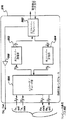
図1を参照すると、レントゲン検査用デジタル画像データを制御し、獲得し、処理するための方法とシステムと装置が示されている。撮像システム100は放射線生成システム109と画像検出システム112とホストコンピュータ114と検出器フレーミングノード304を備える。ホストコンピュータ114はモニタ119とホストプロセッサ115とホストメモリ117を含む。本発明の一実施形態によれば、撮像システム100は画像検出監視システムである。本発明の別の実施形態によれば、撮像システム100の構成要素は1台の装置として機能する。
【0014】
放射線生成システム109はオブジェクト106を通過し、画像検出システム112によって検出される放射線を生成する。本発明の一実施形態によれば、放射線生成システム109はオブジェクト106に対する放射線(104)を生成し、焦点を合わせるX線生成部102を含む。本発明の一実施形態によれば、放射線104はX線である。本発明の別の実施形態によれば、放射線104は連続して生成された複数の放射線群発波とみなされる。本発明の一実施形態によれば、オブジェクト106は人体である。オブジェクト106を通過すると、X線104はX線撮影画像108を形成し、これはその後の検出に使われる。一般的に、X線制御システム110から出力された制御信号に応答して、X線生成部102によってX線が生成される。X線撮影画像108は画像検出システム112によって受信され、X線撮影用デジタル画像に変換される。次に、X線撮影用デジタル画像は画像検出システム112から出力され、ホストコンピュータ114に送られる。ホストコンピュータ114は、放射線生成システム109と画像検出システム112を電子的に制御する。
【0015】
画像検出システム112はX線撮影画像108を受信するためのフラットパネル検出器116を含む。フラットパネル検出器116は動作中に熱くなるため、電力を供給し、冷却するための電源/チラー118に接続される。X線撮影用デジタル画像はフラットパネル検出器116からホストコンピュータ114へ出力される。
【0016】
図2(従来技術)はフラットパネル検出器116の上方概観図である。フラットパネル検出器116は、X線撮影の際の画像レセプタを備える一つの検出技術である。例えば、フラットパネル検出器116によって、既存のX線撮像フィルム、例えば、単純フィルムやスポットフィルムはX線撮影の用途に置き換えられる。また、薄型パッケージであるため、フラットパネル検出器116は、デジタルX線撮影用の、また、蛍光間接撮影やデジタル蛍光透視用の撮像増圧器とビデオカメラとシネカメラとフォトスポット撮像等と置き換えられる。心臓/外科用デジタルX線パネルのフラットパネル検出器116の領域は26cm×26cm、X線撮影用デジタルX線パネルの場合は、45cm×56cm、乳房撮影用デジタルX線パネルの場合は29cm×34cmである。ガラスプレート126と金属の筐体128によってX線レセプタと電子検出機器とそれに関連するエレクトロニクスの周りを囲んでそれらを物理的に保護する。
【0017】
図3(従来技術)は、図2のラインIII−IIIに沿ったフラットパネル検出器116の分解断面図である。図示されているように、X線撮影画像108は、ガラスプレート126を通過し、X線検出パネル134に吸収される。本発明の一実施形態によれば、X線検出パネル134はX線検出用の一枚パネルである。X線検出パネル134はアモルファスシリコンのX線検出パネルである。X線検出パネル134は、X線撮影画像108を光学的なX線撮影画像132に変換する蛍光層130を含む。蛍光層130は、X線検出パネル134、特にアモルファスシリコンパネル136に蒸着される。蛍光層130はガドリニウム酸硫化物Gd2O2S:Tb、もしくはヨウ化セシウムCsI(TI)の形態をとる。高エネルギーのX線を受信する場合は、ヨウ化セシウム蛍光層が用いられる。
【0018】
アモルファスシリコンパネル136は、光学的X線撮影画像132を受信し、複数の代表的な画像データ値138に変換するフォトダイオード/トランジスタアレイである。画像データ値138は配線エレクトロニクス140によってアナログ形式で受信され、アナログ画像データとしてパネル136から出力される。本技術分野では既知の半導体技術によって、蛍光層130とアモルファスシリコンパネル136と配線エレクトロニクス140はシリコンガラス基板上に形成される。同時に、蛍光層130とアモルファスシリコンパネル136と配線エレクトロニクス140とガラス基板144はX線検出パネル134を構成する。
【0019】
図4(従来技術)は金属筐体128から取り出されたX線検出パネル134の上方概観図である。図4(従来技術)に示されるように、アモルファスシリコンパネル136は複数の光電セル146を形成する。各光電セル146から出力された電気情報は対応する複数のコンタクトフィンガー150によってコンタクトリード148に送信される。コンタクトフィンガー150はコンタクトリード148とアモルファスシリコンパネル136間を接続する。図示されているように、蛍光層130はアモルファスシリコンパネル136の上部に形成される。
【0020】
X線検出パネル134は光センサアレイを狭い要素間隔で備え、また、多数の要素を備えて、射影されたX線撮影画像を適切に受信して検出する。アモルファスシリコンパネル136は比較的大きなガラス基板144上に形成された薄膜技術である。プラズマ加速化学蒸着法(「PECVD」)とスパッタリングとメニスカス被覆法によって絶縁体と様々な金属とアモルファスシリコンの11層が蒸着され、電界効果トランジスタ(「FET」)とダイオードと配線とコンタクトが形成される。X線検出パネル134は産業用と医療用のパネル、特に20cm×20cmの心臓/外科用デジタルX線パネルと、41cm×41cmのX線撮影用デジタルX線パネルと、19cm×23cmの乳房撮影用デジタルX線パネルを形成する。心臓/外科用デジタルX線パネルは200μmピッチで1024列×1024行、X線撮影用デジタルX線パネルは200μmピッチで2048列×2048行、乳房撮影用デジタルX線パネルは100μmピッチで1920列×2304行をそれぞれ有する。
【0021】
フラットパネル検出器を形成する場合、アモルファスシリコンには単結晶シリコンよりも多くの利点があり、特に、アモルファスシリコンは単結晶シリコンと区別可能である。アモルファスシリコンは、一定の形式を持たず、また実際の、即ち明らかな結晶構造をもたないことを特徴とする。一方、単結晶シリコンは、単結晶として成長し、ウエハーにスライスされ、さらに不純物を取り除くために研磨されて集積回路となる。アモルファスシリコンは単結晶構造を用いていないため、単結晶シリコンよりも大きなパネルを形成できる。しかしながら、アモルファスシリコンには、100倍から1000倍の欠点の増加と、信号ラグ特性や信号オフセット特性に影響する切り替え速度の大幅な減少が見られる。蛍光層130、CsI(TI)はX線を光線に変換し、アモルファスシリコンパネル136上に蒸着されて密に接続される。CsI(TI)は、複数の光導体と同様に動作する針状構造を構成して、光が外へ広がることを防ぐ。また、CsI(TI)はアモルファスシリコン層136の量子効率に十分適合した伝送スペクトルを提供する。
【0022】
図5(従来技術)はアモルファスシリコンパネル136上に形成された光電セルアレイ152の概略図である。図示されているように、行ライン(n),(n+1),(n+2)...等のスキャンに応答して、複数の光電セル154が順次トリガされる。従って、列ライン(m),(m+1),(m+2)...等に沿って対応する出力が読み出される。各光電セル154はフォトダイオード156と電界効果トランジスタ158を含む。フォトダイオード156はバイアスライン160によってバイアスされ、電界効果トランジスタ158によって適切な時に放電される。電界効果トランジスタ158は対応する適切な列ラインからの放電を制御する。動作中、電界効果トランジスタ158は、適切な行ラインに約+11Vの高電圧をかけることによってオンとなる。電界効果トランジスタ158は、適切な行ラインに約−11Vの低電圧をかけることによってオフとなる。
【0023】
X線照射によって、アモルファスシリコンのフォトダイオード156に正孔対が生成され、X線検出パネル134に部分的な放電が起こる。続いて、電界効果トランジスタ158がオンになると、フォトダイオード156が再充電されて、フォトダイオード156の再充電に必要な電荷量が測定される。動作中、X線照射時は全行ラインがオフ、即ち、−11Vとなる。次に、行ラインが順次オン、即ち、+11Vとなる。行「n+1」が読み出されるときに行「n」からの出力がアナログ情報からデジタル情報に変換されるように、適切な列ライン上の信号のA/D変換がパイプライン化される。A/D変換に利用される期間は、ほぼ各行ラインの読み出しに利用される時間である。
【0024】
図6(従来技術)は本発明の一実施形態に係るフラットパネル検出器116の電気接続の概略図である。フラットパネル検出器116は一つのアモルファスシリコンと、複数の行マルチチップモジュール164と複数の列マルチチップモジュール166に電気接続されたX線検出パネル134を備える。行マルチチップモジュール164からの連続するトリガ信号に応答して、全列が列マルチチップモジュール166に読み出される。列マルチチップモジュール166は検出パネル134から読み出されたアナログ読み出し信号をデジタル信号に変換する。これらの信号はその後リファレンス/レギュレータボード122で受信される。
【0025】
リファレンス/レギュレータボード122は列マルチチップモジュール166から出力されたデータを結合し、そのデータを検出器制御ボード124に出力する。即ち、行マルチチップモジュール164は電界効果トランジスタ158をオン/オフする。一方、列マルチチップモジュール166はそれぞれ列信号を読み出す。リファレンス/レギュレータボード122は、検出器制御ボード124と制御/データ信号を通信しながら、行モジュールと列モジュールに電圧を供給する。
【0026】
図7(従来技術)は本発明の別の実施形態に係るフラットパネル検出器116の電気接続のブロック図である。フラットパネル検出器116は、例えば、心臓/外科用デジタルX線パネルとX線撮影用デジタルX線パネルに見られる電気接続の概略を表す。図示されているように、フラットパネル検出器116は第1パネル部172と第2パネル部174を有する心臓/外科用スプリットパネルX線検出パネル170を含む。本発明の一実施形態によれば、スプリットパネルX線検出パネル170は心臓/外科用スプリットパネルX線検出パネルである。第1パネル部172と第2パネル部174はそれぞれ行マルチチップモジュール176によってトリガされる。第1パネル部172からの出力は第1列マルチチップモジュール178に受信され、第2パネル部174からの出力は第2列マルチチップモジュール180にそれぞれ受信される。
【0027】
図8(従来技術)は、心臓/外科用デジタルX線パネル182としてのスプリットパネル、例えばスプリットパネル170の一実施形態の概略図である。心臓/外科用デジタルX線パネル182は第1パネル部184と第2パネル部186から構成される。スキャンライン0から511は第1パネル部184と第2パネル部186で見られる。従って、行スキャンライン0がトリガされると、2本の行表示ライン、即ち、0と1023が同時にアクティブになり、第1パネル部184と第2パネル部186から対応する列出力ラインが出力される。同様に、第1パネル部184と第2パネル部186で行スキャンライン1が同時にアクティブになると、第1パネル部184と第2パネル部186から対応する列出力ラインが出力される。対応する各パネル部からの各スキャンラインがアクティブになると、各パネル部からの全ての列出力ラインからそれぞれの値が出力される。従って、行スキャンライン0がアクティブになると、第1パネル部184から列出力ライン0−1023が同時に出力され、また第2パネル部186から列出力ライン1024−2047が同時に出力される。
【0028】
図9(従来技術)は、列マルチチップモジュール178、180と、リファレンス/レギュレータボード122のブロック図である。列マルチチップモジュール178は第1パネル部172から出力された列信号を受信し、第2列マルチチップモジュール180は第2パネル部174からの列出力信号を受信する。従って、第1列マルチチップモジュール178からの出力はリファレンス/レギュレータボード122によって結合され、結合された信号出力188は検出器制御ボード124によって受信される。同様に、列マルチチップモジュールは列1024−2047から出力された列信号を受信し、それらを結合し、リファレンス/レギュレータボード122に転送する。リファレンス/レギュレータボード122は受信した信号を結合し、その後結合された信号出力189を出力する。出力188や出力189を含む、リファレンス/レギュレータボードからの結合された出力信号を集めたものが出力195である。
【0029】
リファレンス/レギュレータボード122はマルチチップモジュール178からの出力を結合するための第1の結合部192と、列1024−2047に対応するマルチチップモジュール180からの出力を結合するための第2の結合部194を含む。各マルチチップモジュール178は8個のアナログ読み出し用チップ(「ARC」)196を含み、それらのチップはデジタル読み出し用チップ(「DRC」)198に対応する出力を提供する。従って、DRC198からの出力はリファレンス/レギュレータボード122によって受信される。
【0030】
各ARCチップ196は非線形ランプ比較型A/D変換器を利用する。また、各ARCチップ196は32本のアナログ入力を受信し、データを8ビットチャネルの12ビットシリアル、グレースケールコード化マルチプレクスデータに変換する。次に、各DRCチップ198は4個のARCチップ196から12ビットシリアル、グレーコード化マルチプレクスデータを受信し、シリアルからパラレルへ変換し、グレーコードを12ビットバイナリコードに変換する。各ARCチップ196は受信データをアナログからデジタルに変換するが、これは、全ARC196の全チャネルに共通のD/Aコンバータによって生成された平方根コード化ランプと、コンパレータの各データラインからの信号を比較することによって行われる。ランプ電圧は一定のクロック速度にあわせて増加する。ランプ電圧が保持電圧と一致すると、コンパレータはトリップして、ランプカウンタ値がラッチされる。各データラインの変換時間は、少なくとも受信した全ての列データラインを変換するために用いられる最小クロック数とクロック周期の積の時間と同じくらい長い。信号数が増加すると、ランプ電圧ステップが増加する。量子雑音は各信号の平方根として増加するため、雑音が一定比率となるステップサイズでランプ電圧ステップは二次関数的に増加する。前述の方法によって、行モジュールと列モジュールへ向かう制御信号のインタフェース条件では、約32.5MHzのクロック信号を用いて列モジュール178、180と検出器制御ボード124間のデータ出力をバッファリングする。
【0031】
図10(従来技術)は検出器制御ボード124のブロック図である。一般的に、検出器制御ボード124は、第1列マルチチップモジュール178からの出力188に対応する12ビットバイナリコード化データ「A」を受信する。また、検出器制御ボード124は、第2列マルチチップモジュール180からの出力に対応する12ビットバイナリコード化データ「B」も受信する。入力されたバイナリコード化データA、Bは各々レジスタ200、202に受信される。レジスタ200、202からの出力はそれぞれデコードルックアップテーブル(「LUT」)204、206に転送される。デコードLUT204、206はランダムアクセスメモリであって、12ビットバイナリの二次関数的コードデータを15ビットバイナリの線形コード・データに変換する。
【0032】
検出器制御ボード124の動作は制御部208によって制御される。制御部208はフィールドプログラマブルゲートアレイ(「FPGA」)として構成される。制御部208はデコードLUT204から16ビットの画素データと、デコードLUT206から16ビットの画素データを受信し、その画素データを結合して32ビットワードにする。その後、32ビットワードは画像通信インタフェース210に出力される。本発明の一実施形態によれば、画像通信インタフェース210は光ファイバーインタフェースである。各32ビットワードは2つの16ビット画素の組み合わせであって、検出器制御ボード124から別々に出力される。各32ビットワードに含まれる2つの画素は、(以下に詳細に示され、また図13(従来技術)を参照して)一枚の乳房撮影用デジタルX線パネル224のように並んでいる、即ち、2枚のパネル、例えば心臓/外科用デジタルX線パネル182の第1パネル部184と第2パネル部186の出力から交互に受信される。以下に示され、また、図11(従来技術)を参照すると、X線撮影用デジタルX線パネル228は2つのパネル部230、232を含むので、心臓/外科用デジタルX線パネル182の画素フォーマットを備える。心臓/外科用デジタルX線パネル182とX線撮影用デジタルX線パネル228に対応するスプリットパネル検出システムは、データを「再配列」した後で、従来のコンピュータのモニタ上に表示する。検出器フレーミングノード304でのデータの再配列について以下で詳述する。
【0033】
画像通信インタフェース210は制御部208から受信した32ビットワードをエンコーダ/デコーダ部212にクロック同期で送る。エンコーダ/デコーダ部212は受信した各32ビットワードをエラー訂正機能を有する4つの10ビットワードに変換する。10ビットワードは続いてトランスミッタ214で受信される。トランスミッタ214は受信した10ビットワードを2ビット、即ち、クロックビットとシグナルビットを有するシリアルデータに変換する。トランスミッタ214は2ビットデータを光ファイバートランシーバ216に出力し、光ファイバー信号に変換する。続いて、光ファイバー信号は画像検出バス377を介して以下に詳細に示される検出器フレーミングノードに送信される。本発明の一実施形態によれば、画像検出バス377は光ファイバーデータリンクである。同様に、光ファイバートランシーバ216は画像検出バス377から光ファイバー信号を受信し、その受信した光学信号は2ビットデータに変換され、レシーバ218によって受信される。続いて、レシーバ218は、クロックとデータ信号を含む2ビットの受信データをエラー訂正機能を有する10ビットワードに変換する。続いて、10ビットワードはエンコーダ/デコーダ部212によって受信され、レジスタ220に記憶された後、制御部208に送信される32ビットワードに変換される。また、光ファイバートランシーバ216からの出力は光ファイバー信号検出部222によって受信され、制御部208と共にタイミング/プロトコルを維持する。制御部208は発振器224からクロックで動作する。制御部208は制御ライン226を介してリファレンス/レギュレータボード122に制御信号を提供する。制御部208はカリフォルニア州サンノゼにあるアルテック社製のFPGA,Flex10k50である。
【0034】
図11(従来技術)は、X線撮影用デジタルX線パネル228としてのスプリットパネル検出器、例えばスプリットパネル170の概略図である。X線撮影用デジタルX線パネル228は第1パネル部230と第2パネル部232から構成される。X線撮影用デジタルX線パネル228は41×41cmであって、200μmピッチで合計2048列×2048行を有する。フラットパネル検出器116に関して図示された実施形態は、図7の実施形態と比べて、2倍の行マルチチップモジュール176と2倍の列マルチチップモジュール180を有する。各スキャンラインが順次トリガされる時、列出力ライン0から2047は全て第1パネル部230から画素情報を同時に出力する。また、列出力ライン2048から4095は第2パネル部232から画素情報を同時に出力する。X線撮影用デジタルX線パネル228は心臓/外科用デジタルX線パネル182の表面積のおよそ4倍を占める。X線撮影用デジタルX線パネル228は、広い表面積が必要な用途、例えば胸部X線に用いられ、心臓/外科用デジタルX線パネル182は、より小さい表面積を必要とする処置での用途、例えば外科的処置での心臓の蛍光透視に用いられる。
【0035】
図12(従来技術)は本発明の別の実施形態に係るフラットパネル検出器116の電気的接続のブロック図である。フラットパネル検出器116は、行マルチチップモジュール238によってトリガされる一枚パネル236を含む。一枚パネル236は列マルチチップモジュール240、242によって読み出される。偶数番号の列が列マルチチップモジュール240によって読み出され、奇数番号の列が列マルチチップモジュール242によって読み出されるように、列マルチチップモジュール240,242は一枚パネル236の反対側に配置される。一枚パネル236をハードウェアと接続するために、物理的空間を追加できるようにして、一枚パネル236の反対側から列を交互に読み出すことによって、列密度が高められる。
【0036】
図13(従来技術)は、乳房撮影用デジタルX線パネル244としての一枚パネル検出器、例えば一枚パネル236の一実施形態の概略図である。乳房撮影用デジタルX線パネル244は19×23cmであって、100μmピッチで1920列×2304行を有する。乳房撮影用デジタルX線パネル244は合計2048列を有する。しかしながら、利用可能な2048列のうち実際に用いられるのは1920列である。残りの128列によってデジタルX線パネル244の列全体に間隔が空けられ、容易に修理できる。列出力ラインは乳房撮影用デジタルX線パネル244の交互の側から交互に出力される。本構成によって、製造が容易となり、またハードウェアの乳房撮影用デジタルX線パネル244への接続アセンブリが簡素化される。
【0037】
乳房撮影用デジタルX線パネル244に含まれる128本の修理ラインを用いて、製造上の欠陥により開放となった列アドレスラインを修理する。修理ラインはアドレスラインの両端を横切り、絶縁層によって分離される。レーザを用いて絶縁層からアドレスラインを修理ラインに結合することによって、修理接続が容易になる。行アドレスラインの場合では、行アドレスラインはフラットパネル検出器116上のスペアラインを用いて完全に修理されるため、読み出しシステムが修理を行う必要はない。列の修理の場合では、データが後処理によってソートされるように、修理ラインからのデータはフラットパネル検出器116から異なる順番で出力される。
【0038】
図14(従来技術)は、本発明の別の実施形態に係るフラットパネル検出器116の電極接続のブロック図である。フラットパネル検出器116は2つの行マルチチップモジュールセット、即ち、第1行マルチチップモジュール248と第2行マルチチップモジュール250を含む。第1、第2列マルチチップモジュール178、180とは異なり、第1、第2行マルチチップモジュール248、250は、パネルの行を横切って冗長に接続される。従って、もし、第1もしくは第2パネル部172もしくは174に欠陥があるならば、オプションとして、各行をその別の側からトリガすることによって、行の完全性が保持される。
【0039】
上に示されたフラットパネル検出器116の各実施形態は、冗長な行マルチチップモジュール250によって構成され、パネル構成に欠陥がある場合にデータの完全性を保持することができる。
【0040】
図15はリアルタイムのレントゲン検査撮像システム300のブロック図である。システム300は様々な医療向けアプリケーションに用いられ、また、設計や製造やデバイスの試験と修理にも用いられる。システム300は複数の様々な検出器パネルをサポートし、特に、検出器パネル設計の異なる3つのファミリ、即ち、心臓/外科用とX線撮影用と乳房撮影用のアプリケーションをサポートする。システム300はスクリプト309からユーザアプリケーション301を実行するホストコンピュータ114を含む。獲得部DLL313とDFNデバイスドライバ314によって、ユーザアプリケーション301は検出器フレーミングノード304と通信する。
【0041】
システム300は、リアルタイムオペレーティングシステム、VXWORKS(登録商標)を用いたTMS320−C80プロセッサとPCに基づく従来の画像検出コントローラサブシステム(「IDC」)に取って代わるものである。システム300は1秒間に30フレームを獲得し、蛍光透視用の1024×1024画素の画像処理を行う。画像検出バス377は、ホストコンピュータ114と検出器制御ボード124間に1.25Gビット/秒の光ファイバー通信リンクを提供する。画像検出バス377によって、特に、画像検出システム112の検出器制御ボード124とコンピュータ通信バス302との接続に適した周辺部配線(「PCI」)カードとして具体化される検出器フレーミングノード(「DFN」)304間の通信が行われる。本発明の一実施形態によれば、コンピュータ通信バス302はPCIバスであって、特に、33MHzで動作するPCIバスである。本発明の別の実施形態によれば、コンピュータ通信バス302は66MHzで動作するPCIバスである。検出器制御ボード124自体は、ウィスコンシン州ミルウォーキーにあるジェネラルエレクトリックメディカルシステムズ社製のアポロ共通検出器制御用プリント配線基板(「PWA」)で具体化されている。アポロ共通検出器制御用PWAは、乳房デジタル撮影法の全分野(「FFDM」)を含む様々な用途に用いられる。検出器フレーミングノード304を用いることによって、画像獲得後の画像処理に非リアルタイムホストコンピュータ114の利用が容易になる。
【0042】
市販されている一つもしくは複数のプロセッサPCハードウェア、例えば、カリフォルニア州サンタクララにあるインテル社製のPENTIUM(登録商標)クラスのプロセッサに基づいて、システム300は獲得と制御を行う。システム300は、現在と期待されるX線物療法による一データ獲得/制御システムであって、設計と製造の両方に対するシステムアプリケーションをサポートする。柔軟なアーキテクチャを備えて、技術の改良や将来技術に対するニーズに焦点を当てている。
【0043】
システム300はサポートされている検出器のパラメータをフレーム間で制御することによって、画像の一つもしくは複数のフレームの獲得をサポートする。獲得された画像の行数と列数は入力パラメータとしてサポートされ、外部のフレームトリガによってデータ獲得タイミングを制御する。1024×1024アレイの場合は30フレーム/秒で、また2048×2048画像の場合は7.5フレーム/秒で、システム300はゲイン/オフセット訂正画像を獲得して表示する。システム300は非リアルタイム・オペレーティングシステムをサポートし、システムの機能性をテストする。有効な一実施形態によれば、非リアルタイム・オペレーティングシステムはWINDOWS NT 4.0(登録商標)であって、C++言語ベースのアプリケーションをサポートする。モジュラーソフトウェアはアプリケーションの結合と上級ユーザやプログラマに対してより直接的なハードウェアアクセスをサポートするように構成されている。ユーザによってコード化されたテストアプリケーションや一般化されたデータ獲得ルーチンは別々のモジュールに提供される。
【0044】
システム300は、一つもしくは複数のフレーム領域を含む、一つもしくは複数のフレームの生データとゲイン/オフセット訂正データの両方を保管できる。一つもしくは複数のフレームと一つもしくは複数のフレーム領域の高分解能表示では、新たに獲得されたデータと保管されたデータの両方をサポートすることができる。放射線生成システム109、もしくはグリッド制御されたX線管は、リアルタイムバスインタフェースを介して制御される。2μ秒のタイミング分解能を有するX線生成器をリアルタイムでトリガする処理は、最大16秒までの時間遅延をプログラマブルに制御することによって支援される。
【0045】
システム300はリアルタイム画像データ獲得システムであって、このシステムでは画像データが所定のフレームレートで獲得され、獲得される画像フレーム数は獲得時に決定される。獲得前に、イベントコンパイラ408は、リアルタイムバス379を介して反復トリガの実行時間を設定することによってフレームレートを設定する。同様に、反復トリガから画像検出システム112への画像リクエストコマンドを遅らせることによって、イベントコンパイラ408は画像の獲得のための設定を行う。フラットパネル検出器116のスキャン前にインテグレーション期間があって、この期間で蛍光体で遅延が起こり、また、フォトダイオードアレイの正孔対の収集が可能になる。リアルタイムデータ獲得するために、画像検出システム112から検出器フレーミングノード304へ画像データを転送する際に最小のバッファリングを行うことによって、画像検出システム112と検出器フレーミングノード304が同期して動作することができる。
【0046】
本発明の一実施形態によれば、システム300は以下のように構成される。

システム300は上記の従来のIDCテストシステムを改良したものである。上述のリアルタイムパラメータは、従来技術のVXWORKS(登録商標)オペレーティングシステム(「OS」)で一枚のPCIカードとして動作するように具体化された検出器フレーミングノード304で捕らえられる。検出器フレーミングノード(「DFN」)304は、ファイバーチャネル通信回路とバッファメモリとPCI通信コントローラとX線生成器を制御するリアルタイムバスとDFN304上の全回路を制御するファームウェアプログラマブルFPGAセットを備える。外付けPCIメモリカードをDFN304と共に用いてコンピュータメモリを拡張し、生の画素X線画像データを記憶する。データ獲得動作とその後のデータ処理はユーザが作成したアプリケーションから行う。関数ライブラリからハードウェア機能がアクセスされ、設計やデバイスの修理/製造領域でのユーザの様々なニーズが支援される。
【0048】
図15は、特に本発明の一実施形態に係るシステム300の動作を示す。特定の画像を獲得するためには、正確な一連の画像フレームとそれに関連する獲得パラメータが必要である。従って、フレーム毎にX線パルスに対する読み出し遅延や検出器パラメータ等を特定することができる。それらの属性の記述情報はスクリプト309のフレームシーケンス310で捕らえられる。プログラムアプリケーションは、フレームシーケンス構造によってデータ獲得システムを構成し、システムにトリガを与えてフレームの獲得を開始する。フレームシーケンス310は、テスト毎に実行される試験の種類によって異なる。ハードウェアレベルでは、ホストコンピュータ114からのインストラクションシーケンスに応じて獲得が行われる。本発明の一実施形態によれば、インストラクションはイベントインストラクションであって、総称してイベントシーケンス312として既知である。各イベントインストラクションは十分な時間間隔で実行される。イベントインストラクションは外部デバイス、例えば、バスインタフェースを介して通信するコマンドから制御するイベントをトリガする。例えば、イベントインストラクションは、画像検出バス377を介して画像検出システム112に送信される32ビットの制御ワードと、リアルタイムバス379を介して放射線生成システム109に送信されるX線パルストリガコマンドを含む。フレームシーケンス310に基づいて、実行されるそれらのイベントインストラクション全体のリストが構成される。イベントシーケンス312はリアルタイムに構築されなくてもよいため、非リアルタイム・オペレーティングシステムを実行するホストコンピュータ114上で容易に実行され、イベントコンパイラをサポートできる。一旦、イベントシーケンス312が認識されると、リアルタイムに実行するために、詳細情報がDFN304に送信される。
【0049】
図15は画像獲得中のシステム300からの制御情報/データフローを示すブロック図である。図示されているように、フレームシーケンス310はスクリプト309によって作成される。ターゲット制御ハードウェアの詳細を認識しているコンパイラによって、フレームシーケンス310はイベントシーケンス312に翻訳される。イベントシーケンス312はテスト制御部311によって受信され、コンピュータ通信バス302を介してDFNデバイスドライバ314に送信され、最後に検出器フレーミングノード304に送信される。次に、実行の準備のためにイベントシーケンス312が記憶される。コンピュータ通信バス302を介してBegin Sequenceコマンドを送信することによって、イベントシーケンス312が開始される。ホストコンピュータ114に割り当てられたリアルタイム制御の範囲は、イベントシーケンス312を開始する時期を決定することに限定される。その後、ホストコンピュータ114は画像獲得処理から完全にはずされる。
【0050】
イベントシーケンス312が完了すると、ホストコンピュータ114は獲得したデータの他に、イベントシーケンスの実行中に記録された様々な診断と効果を検索する。従って、ホストコンピュータ114には前処理/後処理の役目も含まれるため、リアルタイム動作からは完全に除外される。
【0051】
図示されているように、検出器フレーミングノード304は、獲得制御部324によってコンピュータ通信バス302を介してコマンドとその応答の通信を行う。獲得制御部324によってイベントシーケンス312はイベントキュー322と通信する。イベントキュー322からイベントインストラクションが放射線生成システム109に送信される。放射線照射中に、画像検出システム112からイベントインストラクションがイベントキュー322に送信される。また、画像検出システム112からフレーム記憶部325によってレントゲン検査画像データが受信され、ホストコンピュータ114に送信するために獲得制御部324に送信される。ホストコンピュータ114では、画像データ316がDFNデバイスドライバ314と獲得ダイナミックリンクライブラリ(「獲得部DLL」)313を介して転送され、その後、ゲイン/オフセット/欠陥画素補正部318によってゲインとオフセットと欠陥画素が補正される。補正が完了すると、テスト演算部320とインタフェースされた後に、画像データはディスクアーカイブ308に送信される。
【0052】
図16は、リアルタイム・レントゲン検査撮像を行うためのソフトウェアシステム328のブロック図である。ユーザアプリケーションインタフェース(「API」)330は、ホストコンピュータ114上で実行されて獲得ハードウェアをユーザアプリケーション301にリンクするソフトウェアである。獲得部DLL313は、ソフトウェアシステム328内の要素と通信するソフトウェアである。獲得部DLL313は、ユーザAPI330とDFNデバイスドライバ314と双方向通信を行う。図示されているように、DFNデバイスドライバ314は検出器フレーミングノード304と双方向通信を行い、その後、放射線生成システム109と画像検出システム112と通信する。また、ユーザAPI330は、表示ライブラリ335と画像処理ライブラリ336とアーカイブライブラリ337と通信する。
【0053】
ソフトウェアシステム328と通信するために、エクセルユーザインタフェース339にインストラクションが準備され、トランスレータ331によって翻訳された後、パールスクリプト部333によって受信される。また、イベントコンパイラ408はバイナリファイル部329に情報を出力する。ユーザAPI330と獲得部DLL313とDFNデバイスドライバ314に制御されて、バイナリファイル部329からの出力情報がEP374上のEABメモリ474にロードされる。バイナリファイル部はイベントシーケンス312を制御する情報を含む。イベントシミュレータ407にタイミング情報を作成する高分解能ディスプレイ338上でイベントシーケンス312をデバッグすることができる。
【0054】
図17は、リアルタイム・レントゲン検査撮像を行うためのハードウェアシステム340のブロック図である。ハードウェアシステム340はデータ獲得/制御ハードウェアを含む。また、ハードウェアシステム340はテスタハードウェアのブロック図である。検出器フレーミングノード304以外のハードウェアの構成要素は市販されている(「COTS」)。ホストコンピュータ114はホストプロセッサ115によって制御される。本発明の別の実施形態によれば、ホストプロセッサ115は共に動作する一対のプロセッサとして構成される。本発明のさらに別の実施形態によれば、ホストプロセッサ115は、配線された複数のプロセッサとして構成される。ホストメモリ117は以下に詳述されるコンピュータRAM334とPCI RAMカード336によって構成される。ハードウェアシステム340は、60Mバイト/秒のデータ転送速度に対応する30フレーム/秒で1024×1024の画像(2Mバイト)を受信する。コンピュータ通信バス302は、132Mバイト/秒の転送速度を有する。第1PCIサブバス342の調整によって、コンピュータ通信バス302を通過する転送速度は132Mバイト/秒より遅くなる。
【0055】
ハードウェアシステム340は、コンピュータ通信バス302に接続されるDFN304を含む。コンピュータ通信バス302は、ブリッジ344によって接続された第1PCIサブバス342と第2PCIサブバス346からなる。第2PCIサブバス346は、小型コンピュータ用周辺機器インタフェース(「SCSI」)348によってディスクアーカイブ308と接続される。また、第2PCIサブバス346は、PCIグラフィックスカードによって高分解能ディスプレイ338に接続される。第2PCIサブバス346は、ブリッジ352によって、ホストプロセッサ115と加速グラフィックスポート(「AGP」)256とコンピュータRAM334を接続する。AGP356は、ビデオカード358によってモニタ360を接続する高速グラフィックスポートである。
【0056】
リアルタイムモードでは、30フレーム/秒の連続した表示速度が調停の競合によって決まるように、PCI302バス調停部は、第1PCIサブバス342と第2PCIサブバス346上のデータ転送速度を落とす。ハードウェアデバッグモードでは、DFN304にコマンドを送信することによって、ホストプロセッサ115からDFNハードウェアのテストが開始される。このテストの結果(即ち、悪い、良い)はホストコンピュータ114に返される。このハードウェアデバッグモードを利用して、本明細書で後述されるビルトインセルフテスト(「BIST」)を実行する。リアルタイムモードではDFN304上のバッファメモリからデータが直接コンピュータRAM334に送信され、ほぼ同時に表示される。
【0057】
図18は、検出器フレーミングノード304のブロック図である。画像検出インタフェース376は、(図10(従来技術)を参照して上述された)検出器制御ボード124と通信して、そこから画像データを受信する。本発明の一実施形態によれば、画像検出インタフェース376は光ファイバーインタフェースである。DFNメモリ部380は合計10個の8メガビットSRAMを含む。DFNメモリ部380は5個のフレームバッファメモリ部381を含み、フレームバッファメモリ部381は各々2個の8メガビットSRAMを備える。一フレームバッファメモリ部381が満杯になると、そのメモリ部のデータがコンピュータ通信バス302に読み出され、続いてデータは別のフレームメモリバッファ部381に書き込まれる。例えば、2048×2048の大きな画像はDFNメモリ部380に直接読み出されるが、このとき、データ獲得プロセッサ(「DAP」)372の制御下でデータを書き込んでいる間にデータが再配列される。DAP372とイベントプロセッサ(「EP」)374はFPGAであって、これらを用いてリアルタイムバスインタフェース378を制御する。リアルタイムバスインタフェース378はリアルタイムバス379に接続される。また、画像検出インタフェース376によって、EP374は画像検出バスを介したデータの読み出し/書き込みを制御する。コンピュータ通信インタフェース382は特定用途向け集積回路(「ASIC」)の形態のPCIインタフェースとして具体化され、ローカルバス384とコンピュータ通信バス302間のバス通信を制御する。図示されているように、光ファイバーテストコネクタ390はバス接続用画像検出インタフェース376とDFN制御部370とインタフェースする。
【0058】
撮像システム100は、様々なX線画像パネル設計やアプリケーションのサポートを含むサポートを様々なユーザに提供する。従って、フレキシブルなテストが提供され、様々な画像獲得モードがサポートされる。撮像システム100が利用する獲得モードはターゲットアプリケーションとユーザに対して示される。例えば、少なくとも4つの特定モード、即ち、ハードウェアデバッグとパネル設定とシングルフレームとリアルタイム性がサポートされる。しかしながら、撮像システム100の形式上の能力は一般的にデータ管理と帯域幅を考慮して特定される。
【0059】
図19は、1024×1024の心臓/外科用デジタルX線画像に対する推定処理能力を示す表である。暫定の推定性能と共に様々な動作モードが示される。注目の二つのケースが分類されている。第1のケースはリアルタイムのケースであって、ハードウェアの帯域幅で目的のフレームレート以内でパイプライン化された一シーケンスを獲得し、補正し、表示する。後処理と呼ばれる第2のケースでは、アルゴリズムの複雑さやパネルサイズを考慮すると、ハードウェアの帯域幅が不十分である。結果として、データはリアルタイムに獲得され、記憶され、遅延期間中に処理され、最後に目的のフレームレートで表示される。
【0060】
図19に示されているように、「gbr」は特別にサポートされた3つの補正アルゴリズム、即ち、オフセット補正ではなく、心臓/外科用デジタルX線とX線撮影用デジタルX線と乳房撮影用デジタルX線に対応する補正アルゴリズムを表す。これらは、ゲイン補正(g)と欠陥画素補正(b)と修理ライン補正(r)である。
【0061】
図20は、400MバイトのPC RAMメモリまたは個々のPCIメモリカード上のメモリの利用可能なフレーム記憶部を示す表である。テストモードはハードウェアテストモードを含み、DFN304を介して接続されたPCIハードウェアカードと外部デバイスのステータス/機能情報をアクセスできる。これにはDFN304カード自体と外付けPCIメモリカードと画像検出バス377と検出器制御ボード124と(放射線生成システム109と通信するための)リアルタイムバス379のテストが含まれる。
【0062】
パネル設定モードは、パネル調整時のパネルテストの最初で用いられ、ほぼリアルタイムの視覚化は画像検出システム112と確実に適切に柔軟にコンタクトするために有用である。ここで、一つの処理オペレーションとして、DFN304でデータ獲得と再配列が行われる。データは、PCI RAMカード336をバイパスしてコンピュータRAM334に直接転送される。その他のアプリケーションでは、データはコンピュータRAM334ではなくて、PCI RAMカード336、もしくは別の市販されている画像処理カードに送られる。データがPCI RAMカード336に入れられると、ホストプロセッサ115はその後の処理のためにそのデータをアクセスすることができる。市販の画像処理カードの場合、データはそのカード内でさらに処理された後、コンピュータ通信バス302を介してホストプロセッサ115に送られる。結果として、1024×1024の画像の場合、データは30フレーム/秒で表示され、2048×2048の画像の場合は7.5フレーム/秒で表示される。画像の獲得と表示の間には1フレームもしくは2フレームの遅延がある。データがホストコンピュータ114に直接転送されるアプリケーションでは、利用可能なコンピュータRAM334は記憶するフレーム数が限定される。
【0063】
シングルフレームモードでは、乳房撮影用デジタルX線テスタとX線撮影用デジタルX線テスタが含まれ、比較的少量のフレームが獲得される典型的なアプリケーションが提供される。一つ以上のフレームがDFN304上のDFNメモリブロック380で捕らえられ、再配列され、コンピュータRAM334に転送され、ホストプロセッサ115内で処理され、ゲインとオフセットと欠陥コラムとARC196のチャネルと欠陥画素が補正される。ARC196のチャネル補正にはゲイン/オフセット補正が含まれ、チャネル毎に変化するARCのゲインを補正する。補正後、フレームが高分解能ディスプレイ338に表示される。2048×2048の画像の場合、データ獲得完了から表示までの遅延は0.25秒未満であると予測される。獲得後、少量のフレームがまだコンピュータRAM334の中にあり、表示後にそのアプリケーションで利用可能となる。
【0064】
リアルタイムモードの一実施形態は、心臓/外科用デジタルX線テスタ、もしくはX線撮影用デジタルX線テスタであって、データが順次獲得され、再配列され、処理され、表示されるようなリアルタイムディスプレイを備える。1024×024の画像の場合、データ獲得から表示までの遅延は約0.03−0.06秒である。1024×1024の画像は30フレーム/秒でサポートされる。本モードでは、第nフレームが記憶され、表示される。ここで、nは1から10であって、オペレータの制御下で、1024×1024のデータの最後の60フレームを記憶することができる。
【0065】
図21は、データ獲得/ソフトウェアインフェース動作の制御を実行するソフトウェアテスタインタフェース400の概略図である。ソフトウェアテスタインタフェース400はテスタアプリケーション402を含み、テスタリソース404を介して獲得ハードウェア418をアクセスすることができる。テスタリソース404は、バッチ処理インタフェース406とプログラミングインタフェースライブラリ337とハードウェアドライバライブラリ339を含む。バッチ処理インタフェース406は、コンフィグレーション・ファイル412とシーケンスファイル414と較正ファイル416を含む。ソフトウェアテスタインタフェース400は、ハードウェアドライバライブラリ339とプログラミングインタフェースライブラリ337への直接インタフェースであって、連続して獲得するために有用な高レベルのCコールを備える。また、ハードウェアドライバライブラリ339はソフトウェアライブラリであって、イベントコンパイラを備え、検出器フレーミングノード304上でユーザが定義したフレームシーケンスを詳細なイベントインストラクションに翻訳して、リアルタイムイベントを処理する。
【0066】
プログラミングインタフェースライブラリ337はプログラミングインタフェースであって、画像の獲得に関してテスタアプリケーションの書き込みを支援する。プログラミングインタフェースは明確な機能サブセットを備え、ハードウェアインタフェースはテスタの全機能をアクセスするものである。プログラミングインタフェースライブラリ337は高レベル機能を含んでおり、ハードウェアドライバとユーザアプリケーション、即ち、テスタアプリケーション402間をインタフェースするものである。この層にはハードウェアデバイスを集めて、ステータス情報を記録する機能が含まれる。また、この層によって、ユーザは特定の獲得モードで獲得ハードウェアをコンフィグレーションして、獲得シーケンスを開始することができる。
【0067】
画像獲得の詳細はフレームシーケンスを定義する構造によって特定される。この構造はユーザプログラムによってプログラミングインタフェース内の獲得サブルーチンに送られる。リターン・オブジェクトはデータとヘッダに対するポインタであって、その後ユーザプログラムで利用可能である。別の方法ではは、データは直接ディスクに保存しても良い。起こりうる様々な補正や表示オプションに対して便利なインタフェースは、このレベルで利用可能である。記述値に対する特定のデバイスでのヘッダの解釈は、この層で発生する。
【0068】
ユーザプログラムが利用可能なライブラリ関数の例を以下に示す。
【0069】
1−Get hardware status(ハードウェアステータスの獲得)
2−Configure acquisition system(獲得システムのコンフィグレーション)
3−Acquire and display data sequence(raw) ((生)データシーケンスの獲得と表示)
4−Acquire and display data sequence(corrected)((補正済み)データシーケンスの獲得と表示)
5−Store data sequence to disk(データシーケンスをディスクに記憶)
【0070】
バッチ処理インタフェース406は、プログラミングインタフェースライブラリ337のプログラミングインタフェースのサブセットであって、画像獲得のためのテキストベースのメカニズムを提供する。コンフィグレーション・ファイル412とシーケンスファイル414はテキストファイルであって、フレームシーケンスを獲得するために全ての情報を定義する。この情報を二つのファイルに分割することによって、フレーム間のパラメータの変化が間違いなくサポートされる。最も単純な動作モードでは、ユーザは共通のテキストエディタでこれらのファイルを変更し、コマンドを用いて獲得を開始することが認められている。リターン・ヘッダはコンフィグレーション・ファイルとシーケンスファイルに定義されたように獲得パラメータを反映するものである。
【0071】
シーケンス全体で一定の情報がコンフィグレーション・ファイル412に含まれる。例えば、ファームウェアの改訂番号やシリアル番号やパネルの種類や処理段階やテスタの位置が含まれる。また、コンフィグレーション・ファイル412に含まれる情報には、再配列オプションと補正オプションとアーカイブオプションと表示オプションが含まれる。較正ファイル416は、ゲインとオフセットと欠陥画素と画素毎のARC196のチャネルゲインについてデータを補正するための全情報を含む。対照的に、シーケンスファイル414は、シーケンスの各フレームの特定の獲得パラメータを含む。これらの特定の獲得パラメータは全ての検出パラメータとイベントタイミングを含む。
【0072】
図22は、コンピュータ通信バス302によってシステムコンポーネントと相互作用するハードウェアドライバインタフェース410のブロック図である。ハードウェアドライバインタフェース410は、イベントコンパイラ408の主要素としてノコマンドを含み、フレームシーケンスの記述構造を詳細なイベントインストラクションセットに翻訳し、そのインストラクションセットは検出器フレーミングノード304のイベントプロセッサ374上のキューにロードされる。ハードウェアドライバインタフェース410は、イベントコンパイラ408とハードウェアデバッグツールキット409と外部デバイスに対する複数の外部デバイスサポート411を含む。外部デバイスサポートは、複数の外部デバイス、例えば、検出器フレーミングノード304や高分解能ディスプレイ338等をサポートする。ハードウェアドライバインタフェース410は、バスインタフェースによって外部デバイスと通信する。コマンドを利用して基本的なメッセージを外部デバイスに送信し、応答メッセージ、例えば、検出器のメッセージやX線ステータスメッセージをユーザアプリケーションに戻すことができる。テストシステムの開発には、各ハードウェアをデバッグして検査するためのソフトウェアセットが関わる。ツールキットとしてテスタ製品の一部としてこのソフトウェアを明確な形にし、文書化し、提供して、ユーザや保守管理者によるシステムサポートを支援する。イベントコンパイラ408はソフトウェアパッケージであって、フレームシーケンスファイルを獲得し、DFN304内のDFN制御部370にロードされる制御ワードセットを生成して、所望の制御機能を実現する。
【0073】
図17に示されるように、ハードウェアシステム340はハードウェアとソフトウェアを備え、市販のディスプレイドライバカードの駆動をウィンドーレベルで制御して、データの獲得結果を表示する。ディスプレイは生の保存画像と処理された保存画像の両方を表示する。表示データは、蛍光体の非線形性を示すためのガンマ補正部を含む8ビットである。最低倍率では、表示される最下位ビット(「LSB」)と画像検出システム112から受信した最下位ビットには一対一の相関関係がある。第2のモニタ368を用いてユーザインタフェースが提供される。画像表示部は、Xia機能、例えば、パンやズームや画素振幅の表示をサポートする。オプションとして、選択された画素の行番号と列番号は、注目領域の統計量の演算値と共に表示される。
【0074】
ディスクアーカイブ308は短期記憶に用いられ、取り外し可能ディスクドライブまたは書き込み可能650MバイトCD−ROMで実施される。生画像と処理された画像と共に記述情報のヘッダを保存する能力がサポートされている。
【0075】
ホストコンピュータ114はネットワークサポートを備え、10/100Mビット/秒のイーサネットカードとイーサネットを介してデータ転送を行うためのソフトウェアから構成される。その他のデバイス、例えば、パネルテストで用いられるLEDやコリメータがサポートされる。それらのサポートにはさらに別のPCIカードや、そのPCIカードにデータを収集する、即ち、送信するためのCプログラムのドライバが含まれる。
【0076】
放射線生成システム109を制御したり、それからの制御を受けるために、8ビットリアルタイムパラレルI/Oバス379が用いられる。タイミングはDFN制御部370から提供される。X線生成から検出器制御ボード124上のデータ獲得までの遅延はソフトウェアの制御下で与えられる。従って、データ獲得とX線生成の同期化が行われる。X線生成電圧と電流と共に、テスタハードウェアやソフトウェアを介してX線生成部102をオン/オフする動作は、ソフトウェア制御下で設定される。制御グリッドを用いてX線生成部102がパルス制御される。パルス間の電流/電圧は200m秒の時間分解能で制御される。別の方法では、X線生成器102に個々のインタフェースが提供される。
【0077】
また、8ビットリアルタイムパラレルI/Oバス379を用いて放射線生成システム109のX線生成器102を制御する。DFN304上のDFN制御部370によってタイミングが提供される。X線生成から検出器制御ボード124上のデータ獲得までの遅延はソフトウェアの制御下で与えられる。X線生成器102はオン/オフ信号でトリガされる。別の方法では、生成器の電圧と電流と照射時間が設定されて、測定される。同様に、8ビットリアルタイムパラレルI/Oバス379を用いて、X線撮影用デジタルX線のX線生成器を制御する。
【0078】
図23は、検出器制御ボード124のコンフィグレーション設定を示すブロック図である。ファイバーチャネルインタフェースハードウェアを介して検出器フレーミングノード304は検出器制御ボード124とインタフェースし、1.25GHzの通信レートをサポートする。図23のコンフィグレーション設定を制御することによって、ユーザはデータ獲得処理を制御することができる。
【0079】
図1と図18を参照して、検出器フレーミングノード304によって、ホストコンピュータ114は放射線生成システム109と画像検出システム112とインタフェースすることができる。従って、検出器フレーミングノード304は検出器制御ボード124と通信するためのファイバーチャネルインタフェースと、放射線生成システム109と通信するためのRS−485リアルタイムバスインタフェース378と、ホストコンピュータ114と通信するためのコンピュータ通信インタフェース382をサポートする。DFN304のアーキテクチャのブロック図が図18で示されており、直前で説明したインタフェースを示している。インタフェース通信用のハードウェアと共に2つのFPGAがカードを介してデータフローを制御する。EP374はシーケンサを備え、検出器とX線イベントインストラクションをリアルタイムに組み合わせる。また、EP374はホストコンピュータ114と通信するコマンドインタープリタを備える。DAP372はフレーム読み出し中での画像データのルーティングを制御し、画像検出バス377とローカルバス384とDFNメモリ部380間のブリッジチップとして動作する。
【0080】
検出器フレーミングノード304は、DFN制御部370の形態でプログラマブルロジックに基づくアーキテクチャをサポートする。DFN制御部370は、内蔵プロセッサ上の一対のFPGAから構成されることが好ましい。第1に、FPGA用のファームウェアは、一つのASICに組み込むためにVHDLハードウェア記述言語で書かれ、その大部分は独立したプラットフォームのまま残る。第2に、検出器フレーミングノード304のVHDLシミュレーションによって、ハードウェアの開発時間が短縮される。第3に、プログラマブルロジックデバイスを用いることによって、DFN304の設計の簡素化することができ、DFN304上の様々なクライアント・バス、即ち、画像検出バス377とコンピュータ通信バス302とリアルタイムバス379間の信号のカスタムルーティングが可能となる。コンフィグレーション可能な論理を用いることによって設計とシミュレーションとプログラミングを簡素化することができる。
【0081】
検出器フレーミングノード304は、32ビット、33MHzのコンピュータ通信インタフェース382を用いて60Mバイト/秒の転送レートをサポートする。別の実施形態によれば、コンピュータ通信インタフェース382は64ビットのPCIインタフェースである。DFNメモリ部380は2Mバイトのフレームバッファとして具現化された5個のフレームバッファメモリ部381を含む。各フレームバッファメモリ部381は、損失やデータ中断なしに画像検出バス377からコンピュータ通信バス302への連続したデータ転送を容易にする(バースト転送が発生する)。5個のバッファを用いることによって、損失やデータ中断なしに一乳房撮影用デジタルX線画像を捕らえるための余裕ができる。リアルタイムバス379は8チャネルの全二重リアルタイムバスインタフェース(RS−485)である。
【0082】
検出器フレーミングノード304は、シリアル接続を介して放射線生成システム109を制御する。言い換えれば、検出器フレーミングノード304は、X線生成・外部制御部と直列接続されている。検出器フレーミングノード304は、1.25Gボーレートで動作する画像検出インタフェース376と、32ビット、33MHzのコンピュータ通信インタフェース382と、8ビットのRS−485リアルタイムバスインタフェース378と、検出器イベントインストラクションとX線インストラクションのリアルタイムシーケンスとビルトインセルフテスト(「BIST」)と、フィールドの再生と、パワーダウン能力と、60Mバイト/秒のソフトウェアリセットの連続データスループットと、キー信号の監視をサポートする。BISTは5個のフレームバッファメモリ部381の全て、即ち、10個のSRAMと、画像検出バス377上の電気的ループバックテストと、リアルタイムバス379上の電気的ループバックテストで提供される。
【0083】
検出器フレーミングノード304の主な構成要素は以下に示す表1に基づいて具現化される。
テストと監視を行うために、自己温度監視とユニークボードIDとレイアウト改訂番号とDFN制御部370の再生用のJTAGポート542とFPGA EEPROMの再プログラミングのためのJTAGポート544と視覚的診断インジケータとローカルバスアクセス用のコネクタと画像検出バス377アクセス用のコネクタとDAP/EPテストバス384アクセス用のコネクタが検出器フレーミングノード304によってサポートされる。
【0085】
EP374は、アルテラフレックスファミリ社製−1スピードグレード200KゲートFPGAであって、バスマスタ能力を有する32ビットのローカルデータバスをサポートする。また、EP374は、20ビット・ローカルアドレスバスと32ビット・テストバスとDAP372への32ビットのダイレクトリンクと32ビット・ファイバーチャネル受信用バスと32ビット・ファイバーチャネル送信用バスと12ビット・ファイバーチャネル制御バスと31.25MHzファイバーチャネル基準クロック入力と36/33MHzのローカルバスクロック入力と低電力動作用2.5Vコアと3.3VのTTLコンパチブルインタフェースをサポートする。EP374は8個の視覚的診断インジケータを駆動し、オンボード温度センサとインタフェースする。同様に、EP374は利用可能な5ビットのレイアウト改訂コードを読み出し、ボードIDチップとインタフェースする。
【0086】
DAP372は、アルテラフレックスファミリ社製−1スピードグレード200KゲートFPGAであって、32ビット・ローカルデータバスとバスマスタ能力を有する20ビット・アドレスバスと32ビット・ファイバーチャネル受信用バスと32ビット・31.25MHzファイバーチャネル基準クロック入力と36/33MHzローカルバスクロック入力とローカルバス調停ロジックとSRAMアドレスバスとSRAMデータバスとSRAM制御ラインとSRAMクロックとJTAGバスコントローラと32ビット・テストバスと低電力動作用2.5Vコアと3.3V・TTLコンパチブルI/Oをサポートする。
【0087】
図18は、検出器フレーミングノード304のブロック図である。DFN304によって、ホストコンピュータ114は放射線生成システム109とX線画像検出システム112とインタフェースでき、X線デジタル画像獲得処理を制御する。DFN304は画像検出インタフェース376とリアルタイムバスインタフェース378を含む。DFN制御部370は2つのFPGAからなり、DFN304を介してデータフローを制御する。EP374はシーケンサを備え、検出器とX線イベントインストラクションをリアルタイムに組み合わせる。また、EP374はコマンドインタープリタを備え、コンピュータ通信バス302を介してホストコンピュータ114と通信する。DAP372はフレーム読み出し中の画像データのルーティングを制御し、画像検出バス377とローカルバス384とDFNメモリ部380間のブリッジチップとして動作する。
【0088】
図24は、フィールドプログラマブルゲートアレイ(「FPGA」)440の概略図である。DFN304に内蔵されている機能の大部分は2つのFPGA440をDFN制御部370として用いることによって実現される。FPGA440は高速カスタムロジックとバス集中アプリケーションに用いられる多数のユーザI/Oを備える。DFN304上のロジックは全てVHDLハードウェア記述言語を用いて記述されているので、様々なFPGAアーキテクチャに対して移植性が高い。DFN304に用いられる特定のFPGAは、大量のコンフィグレーション可能な配線と共にロジックアレイブロック(「LAB」)442のマトリクスを含む。図24に示されるように、各LAB442は、それに関連するローカル配線リソースと共に8つの論理要素(「LE」)444にさらに分割される。各LE444は、組み合わせ論理関数を実現するためのルックアップテーブルに基づく4入力SRAMを備え、フリップフロップに接続される。信号はユーザI/Oパッドセルとの間で送受信されるが、ユーザI/Oパッドセル自体はパラメータ、例えば出力立上り時間やオープンコレクタ出力等を変更するようにコンフィグレーション可能である。論理密度や動作速度のためにFPGA440が選択される。
【0089】
図25はEP374のブロック図である。EP374はDFN304の制御デバイスとして用いられる。図25に示されるように、EP374は、互いに通信してDFN304の機能の様々な態様を制御する多数のサブユニットからなる。これらの各サブユニットについて順に議論する。
【0090】
EP制御部450は、EP374の動作を監視し、ローカルバス384とファイバーチャネルインタフェース480とイベントシーケンサ部470間の相互作用を調整する。EP制御部450は、EP374内で生じる様々な動作をパラメータ化する複数の制御レジスタ454と実行中に起きた問題をホストコンピュータ114に記録するために用いられる複数のエラーレジスタ452を保持する。EP制御部450は、マスタ制御部456によってエラーレジスタ452と制御レジスタ454間の相互作用を調整する。
【0091】
PCI/ローカルバスインタフェース部460は、EP374とローカルバス384間の通信のホストとなる。コンピュータ通信インタフェース382とのローカルバス接続を介して、PCI/ローカルバスインタフェース部460は、コンピュータ通信バス302を介してDFN304に送信されるコマンドの主な応答部として機能する。PCI/ローカルバスインタフェース部460は、ホストコンピュータ114からのコマンドを処理するPCIコマンドインタープリタ462を含む。例えば、コマンドには、次のシーケンスのデータとともにイベントシーケンサ部470内のEABメモリ474へイベントキューをロードしたり、開始シーケンスコマンドの処理が含まれる。
【0092】
イベントシーケンサ部470は、EABメモリ474にイベントキューを保管し、シーケンス動作中はイベントインストラクションをデコードし、実行する。イベントキューはEP374上の利用可能なオンチップEABメモリ474を用いて具体化される。EABメモリ474のイベントキューは、最も効率よくメモリリソースを利用するためにバイト単位で構成される。EABメモリ474内でのイベントの順序付けやイベントキューの読み出し/書き込みは、キュー制御部472によって制御される。イベントインタープリタ476によってイベントインストラクションの翻訳が実行される。シーケンス実行中にイベントインストラクションがイベントキューから読み出されるとき、様々なインタフェースから送信されるデータは、それをさらに処理するためにイベントインタープリタ476によってEP374上のその他のユニットに転送される。
【0093】
ファイバーチャネルインタフェース480は、画像検出インタフェース376との通信を保持しなければならない。データは、FC EP送信部484によって送信され、EP FC受信部486によって受信される。リンクの状態は、通信が喪失しているかどうか、または異常状態が起こっているときにホストコンピュータ114に通知するEP FC制御部482によって監視される。36.0MHzのローカルバスクロックで実行されるほとんどのEP374とは異なり、EP FC送信部484は31.25MHzのファイバーチャネル送信クロック584で実行される。同様に、EP FC受信部486はファイバーチャネル受信クロック585で実行される。この非同期動作によって、画像検出バス377とローカルバス384間のレートを変える。ファイバーチャネルインタフェース480内のユニットは、ハンドシェーキング/ダブルバッファレジスタ用のフラグを用いて、残りのEP374と非同期通信を行う。
【0094】
EPリアルタイムバスインタフェース490は、EABメモリ474内のイベントキューからのリクエストを処理するが、このリクエストは、リアルタイムバス379の状態を変更を求めるリクエストである。また、EPリアルタイムバスインタフェース490は、外部デバイス(例えば放射線生成システム109)が強制的にリアルタイムバス379の状態になったとき、イベントキューとホストコンピュータ114に通知しなければならない。
【0095】
EP374に対しては、2本のグローバルクロック入力信号、即ち、GCLK1入力信号492とGCLK2入力信号494がある。これらの入力信号は、2つの専用クロックツリーを用いて、デバイス上の全ての論理に最適に分配置される。EP374では、GCLK1 492とGCLK2 494は、36.0MHzのローカルクロック574と31.25MHzのファイバーチャネル送信クロック584によってそれぞれ駆動される。
【0096】
また、さらに4本の専用グローバル信号ラインがあるが、これらのタイミングは最適化されていない。EP374では、これらは3本のリセット信号トリガ496に接続される。コンピュータ通信インタフェース382によって2本のリセットトリガ(USERoとLCL_rst)が生成され、以下に詳細に示すように、パワーオンリセット回路から第3の信号が発せられる。
【0097】
図26は、DAP372のブロック図であって、DAP372はDFN制御部370で用いられる第2のFPGAである。DAP372は主に、31.25MHzで有効に動作する画像検出バス377から受信したデータと36.0MHzで動作するコンピュータ通信バス302間のレートを変えることに関係する。DAP372は、の画像検出バス377から受信したデータを第1のフレームバッファメモリ部381に記憶することによってレートを変更し、同時に、第2のフレームバッファメモリ部381から以前記憶されたデータをコンピュータ通信インタフェース382を介してコンピュータ通信バス302に読み出す。
【0098】
図26に示されるように、DAP372は多数のサブユニットからなり、これらはDFN304の画像データフローを調整する。まず、DAP FC受信部500では、32ビットの画像データが31.25MHzのファイバーチャネル受信クロックレートで受信される。各32ビットワードは2つの16ビット画素値を備え、各々検出器制御ボード124によって同時に読み出される。結合された32ビットワードは、ファイバーチャネル受信クロックを用いてファーストインファーストアウト(「FIFO」)部502に書き込まれる。同時に、データはDAP FIFO部502から画素再配列部504に非同期に読み出される。画素再配列部504によって実行される再配列機能は、以下に詳細に示される。このデータは36.0MHzのローカルバスクロックレートで処理される。画素は、画素再配列部からクロスバー506に送られ、クロスバーは現在アクティブなフレームバッファメモリ部381に対する画素の経路づけをおこなう。
【0099】
現在アクティブな受信フレームバッファメモリ部381に受信データが記憶されると同時に、以前記憶されたデータが現在アクティブな記憶フレームバッファメモリ部381からコンピュータ通信バス302に読み出される。データは再びクロスバー506で経路づけされる、この場合は、コンピュータ通信インタフェース382に送信され、その後コンピュータ通信バス302に送信される。DFN304内の5つの利用可能なフレームバッファメモリ部381は各々、コンピュータ通信バス302上で通信を終了させる可能性に対処するため、タイミングセーフガードを加える。通信が中断されても、受信回路は続けて画像検出システム112から受信するデータを記憶するが、もしそうでなければ、このデータは失われる。コンピュータ通信バス302が再び選ばれると、データは引き続き36.0MHzのローカルバスクロックレートで転送される。これにより、中断されずにデータを転送でき、また画像検出バス377とコンピュータ通信バス302間のレートを変えることができる。
【0100】
データフローアーキテクチャの一部として、DAP372は、EP374とコンピュータ通信インタフェース382とDAP372間にあるローカルバス384へのアクセスを調整するローカルバス調整器507を備える。実際、クロスバー506とコンピュータ通信インタフェース382間は双方向接続である。この双方向性によって、コンピュータ通信バス302によってアドレス生成器512を直接制御すると同時に、ホストコンピュータ114はフレームバッファメモリ部381の直接読み出し/書き込みが可能となる。
【0101】
図26に示されるように、DAP372はアドレスバスとフレームバッファメモリ部381の読み出し/書き込み信号を制御する。画像フレームコントローラ508は、アクセスされる検出パネルの種類の詳細情報(ライン長、ライン/画像)によってコンフィグレーションが行われ、入ってくる画素データを追跡して適切なフレーミングを維持することを保証する。ライン長もしくはフレームサイズが一貫していないイベントではエラーが生成され、ホストコンピュータ114に報告される。ライン再配列部510は、アドレス生成器512にデータを供給することによって、現在アクティブの受信/記憶フレームバッファメモリ部381に対する適切なアドレスを生成させる。同時に、様々なメモリ部制御信号の正確なタイミングが、読み出し/書き込みサイクル制御部514によって保持される。フレームバッファメモリ部381に関する詳細情報が以下に示される。
【0102】
DAP372へのグローバルクロック入力信号は、GCLK1 516とGCLK2 518の2本である。これらの入力信号は、2つの専用クロックツリーを用いて、デバイス上の全ての論理に最適に分配置される。DAP372上では、GCLK1 516とGCLK2 518は36.0MHzのローカルバスクロックと31.25MHzのファイバーチャネル受信クロック584によってそれぞれ駆動される。また、さらに4本の専用グローバル信号ラインがある。DAP372上では、専用グローバル信号ラインは3本のリセット信号トリガ520に接続される。コンピュータ通信インタフェース382によって2本のリセットトリガ(USERoとLCL_rst)が生成され、以下に詳細に示すように、パワーオンリセット回路から第3の信号が生成される。
【0103】
DAP制御部521はDAP372の動作を監視しなければならない。DAP制御部521は、DAP372で発生する様々な動作をパラメータ化する制御レジスタ524を保持する。また、DAP制御部521は、実行中の問題をホストコンピュータ144に報告するために用いられるエラーレジスタ522を保持する。最初の電源投入時、またホストコンピュータ114からのコマンドに関して正常に動作している間、RAM BIST528は、フレームバッファメモリ部381のビルトインセルフテストを実行する。詳細な情報を以下で示す。
【0104】
図27は、DFN制御部370とパワーオンリセット部535のブロック図である。テスト/デバッグの他にフィールド内のファームウエアの更新を容易にするために、プログラマブルメモリ部329によって、DAP372とEP374のコンフィグレーションを行うことができる。プログラマブルメモリ部329は、DAP EEPROM部532とEP EEPROM部530を備える。別の方法では、DAP372とEP374は、プログラマブルJTAGポートJTAG1 542とJTAG2 544である。典型的なオペレーションでは、最初にホストコンピュータ114に電源が投入されるときに、DFN304に電源が投入される。この段階では、DAP372とEP374の各々は、それぞれのEEPROMからブートするため、それぞれのEEPROMからデータをロードすることによって動作可能となる。図27は、DFN304のコンフィグレーション回路を示す。DAP372とEP374は各々、それに関連するEEPROM部を備えるが、このEEPROM部は、デイジーチェーンされプログラム用記憶場所を備える2つのEPC2チップを備える。DAP372とEP374の各々ののEEPROM部が簡潔に示されている。各EPC2チップはソケット型20ピンPLCCパッケージであって、再プログラミングのために容易に取り外すことができる。図示されているように、コンフィグレーション、即ち、データのロード処理は、シリアルデータを1ラインに供給してデバイスのコンフィグレーションを行う受動シリアルモードで行われる。
【0105】
プログラマブル制御部529は、最初のブートシーケンスインストラクションを記憶し、検出器フレーミングノード制御部370を制御する。制御部570によるリセット、もしくは検出器フレーミングノード304に最初に電源を投入するために、プログラマブル制御部529は、最初のブートシーケンスインストラクションをロードする。本発明の一実施形態によれば、最初のブートシーケンスインストラクションは、ホストコンピュータ114からコンピュータ通信インタフェース382を介して検出器フレーミングノードメモリ部380に更新インストラクションを送ることによって更新される。更新インストラクションは、検出器フレーミングノードメモリ部380からプログラマブルメモリ部529に送られる。JTAGループ545は、更新インストラクションをローカルバス384からプログラマブルメモリ部529に送る。
【0106】
図27に示されるように、DAPパワーオンリセット(「POR」)部536とEP POR部534を用いて、DFN304に電源が投入されてからさらに140m秒の間reconfigラインをロウに保持することによって、コンフィグレーションが完了する。これにより、100m秒の電源立ち上がり時間が確保できなかった場合でも、DAP372とEP374のコンフィグレーションを確実に行うことができる。別の方法では、プッシュボタンスイッチを用いて各POR回路部を手動でディスエーブルにし、電力をボードに循環させずにFPGAを再びコンフィグレーションすることができる。FPGAのコンフィグレーションに関与する全信号ラインは、ボードの最上層で利用可能となっているので、ボードの初期テスト中に問題が検出されたときに、FPGAのコンフィグレーションのデバッグが容易になる。また、DAP372もしくはEP374のリブートを選択的にディスエーブルにするために、ジャンパが提供することによって、コンフィグレーション中、もしくは特定のデバイスによる問題のデバッグが支援される。
【0107】
DFN304のテスト/デバッグ中、図示されたJTAGポート542、544を介して、FPGAのコンフィグレーションとEEPROM部530、532のプログラミングが完了する。FTAG1 542はEP374とDAP372を含むループに提供される。デバッグ、もしくはファームウェアの開発中に問題が生じたとき、実装されていない0オームのレジスタを用いてEP374もしくはDAP372をループから解除させることが可能となる。
【0108】
JTAG2 544は、2つのEEPROM部530,532を含むループに提供され、EEPROM部530,532をプログラムするために用いられる。カリフォルニア州サンノゼにあるアルテラ社製のByte BlasterケーブルとMaxPlusIIソフトウェアを用いて、それぞれのJTAGポートを介してEEPROM部530、532をプログラムすることができる。図28に示されるように、JTAG2 544はDAP EEPROM部532とEP EEPROM部530を含む第2のJTAGループ545に備えられて、EP374とDAP372をプログラムするために用いられる。
【0109】
DFN304がフィールド内に存在するときに、オプションとして、ファームウェアを異なるバージョンに更新することができる。便宜上、ホストコンピュータ114を開けてEEPROMデバイスを最近のバージョンのものに交換せずに、直接更新することができる。EEPROM部のインシステム・プログラミング性能は、上述したように各JTAGポートを介してサポートされる。DFN304によって、Byte BlasterケーブルやMaxPlusIIソフトウェアを用いずに、ホストコンピュータ114は、コンピュータ通信バス302を介して、JTAG1 542やJTAG2 544を直接アクセスできる。
【0110】
図27に示されるように、EEPROM部530,532をJTAG2ポート544からプログラム可能とする第2のJTAGループ545は、ユーザI/Oピンを介してDAP372に接続される。ファームウェアの古いバージョンを用いてボードFPGAが適切にコンフィグレーションされると、EEPROM部は、DAP372に常駐するファームウェアのアプリケーションを用いて再プログラム可能である。EEPROM部のデータはコンピュータ通信バス302を介してフレームバッファメモリ部381に転送される。フレームバッファメモリ部381から、DAPファームウェアによってデータが読み出され、シリアル化され、フォーマット情報やコマンド情報と共に、それぞれのJTAGバスを介して転送される。
【0111】
対応するJTAGバスを介してDAP372が、EEPROM部を再プログラムした後で、DPA372はJTAGコマンドを発行して、EEPROM部に、DAP372とEP374の自動的な再コンフィグレーションを実行させる。EP EEPROM部530とDAP EEPROM部532を構成するEPC2チップの再プログラミングを可能にする試みが一つある。エラーチェック処理によってデバイスが正確にプログラムされることが保証されるが、これではユーザがEPC2に誤ったファームウエアのプログラミングを行うことを防ぐことができない。ソフトウェアインターロックを用いたり、また一般的な予防策によってこの状況は緩和される。EEPROM部は常に物理的にDFN304に戻される。
【0112】
DFN304は5つのフレームバッファメモリ部381にグループ化された10個の9.4MビットSRAMを用いる。以下に詳細に示されるが、SRAMへのアドレスバスとデータバスは、これらのデバイスを制御し画素データ再配列アルゴリズムを実行するDAP372に接続される。SRAMが連続して読み出されるとき、メモリマップド高分解能ディスプレイ333に正確に表示するためにデータを再び整列させるように検出パネルの各行からSRAMへデータを書き込むことによって、各フラットパネル検出器のデータ再配列が行われる。ダイレクトメモリアクセス(「DMA」)用のコンピュータ通信バス302を用いて、データはSRAMからホストコンピュータ114のコンピュータRAM334に転送される。
【0113】
各SRAMは100ピン薄型クワッドフラットパック(「TQFP」)パッケージに含まれる。部品は256K×36として構成され、12n秒サイクルタイムを有する。アドレス信号と、データ入力信号と、出力イネーブル信号とリニアバーストイネーブル信号を除く全ての制御信号はクロックの立ち上がりエッジで真となる。SRAMは36MHzで動作するため、先頭の部分に余裕ができる。通常、データは2つの16ビットワードであるため、各SRAMの下位4ビットは用いられず、有効なメモリ容量は8.4Mビットである。全てのピンが検査のために利用可能であるため、TQFPパッケージによってデバッグが可能となる。しかしながら、BGAパッケージを用いることによって、製造の歩留まりが向上する。DFN304が形成されたボードの各物理的サイドに5つのSRAMを配置することによって、アドレス/データライン長を最小にすることができる。各フレームバッファメモリ部381を構成するSRAM対は物理的なボードのサイドに交互に配置される。
【0114】
一対のSRAMとして構成されるフレームバッファメモリ部381へのデータの書き込みと、一対のSRAMである第2のフレームバッファメモリ部381からのデータの読み出しは同時に発生する。これは、データを処理し、5対の8.4MビットSRAMの対するデータの読み出し/書き込みを行うDAP372に5本の32ビットデータバスと5本の18ビットアドレスバスを提供することによって実現される。従って、600ピンDAP372の250ピンが、SRAMのアドレス用とデータ用に用いられる。
【0115】
18ビット・アドレスバスと32ビット・データバスの他に、用いられるSRAM制御ピンはライトイネーブルピン(WE#)と3本のチップセレクトピン(CS1#,CS2,CS2#)とスリープモードピン(ZZ)である。CS1#を用いて読み出し/書き込み用のSRAMを選択する。CS2とCS2#を用いて、以下に示される心臓/外科用デジタルX線フラットパネルとX線撮影用デジタルX線フラットパネルのデータ再配列スキームを実施する。スリープモードは電力を抑えるために用いられる。#はそのピンがアクティブロウであることを示すことに注意されたい。
【0116】
図28は、心臓/外科用デジタルX線パネル482から読み出されるデータの概略図である。図示されているように、第1の心臓スキャンライン185は第1パネル部184から読み出されるデータラインであって、第2の心臓スキャンライン187は第2パネル部186から読み出されるデータラインである。各スキャンライン185,187はスプリットパネル184,186間の中心方向に向う。一番上のパネルの一番上の行と一番下のパネルの一番下の行から同時に画素を読み出すことによって、スプリットパネルの各々からデータが読み出される。アクティブフレームバッファメモリ部381へのデータ書き込みに備えて、最初の4つの画素(一番上の行からの2つと一番下の行からの2つ)からDAP372にデータが記憶される。
【0117】
心臓/外科用デジタルX線の場合、心臓/外科用デジタルX線パネル182から読み出されるデータは、DFN304のDFNメモリ部380のSRAM A1,A2に記憶される。SRAM A1,A2はフレームバッファメモリ部381を備える。図28は、実際に読み出されるデータとSRAMの対応、即ち、2つのSRAMを表す。DFNメモリ部380は10個のSRAMを有する。
【0118】
図29は、X線撮影用デジタルX線パネル228から読み出されるデータの概略図である。図示されているように、第1のX線撮影スキャンライン231は第1パネル部230から読み出されるデータラインであって、第2のX線撮影スキャンライン233は第2パネル部232から読み出されるデータラインである。各スキャンライン231,233はスプリットパネル230,232間をセンターラインに向かって進む。X線撮影用デジタルX線の場合、X線撮影用デジタルX線パネル228から読み出されるデータは、DFN304のDFNメモリ部380のSRAM A1,B1,C1,D1とA2,B2,C2,D2に記憶される。それぞれの対のSRAM A1,A2とB1,B2とC1,C2とD1,D2は各々、一つのフレームバッファメモリ部381を有する。図29は、実際に読み出されるデータとSRAMの対応、即ち、8つのSRAMを表す。DFNメモリ部380は10個のSRAMを有する。
【0119】
図30は、乳房撮影用デジタルX線パネル244から読み出されるデータの概略図である。図示されているように、乳房撮影スキャンライン245は、乳房撮影用デジタルX線パネル244から読み出されるデータラインである。スキャンライン245は、パネル244を横切って下方向に進む。乳房撮影用デジタルX線の場合、パネル244から読み出されるデータは、DFN304のDFNメモリ部380のSRAM A,B,C,D,E,F,G,Hに記憶される。物理SRAMは上述されたSRAM A1,A2とB,B2とC1,C2とD1,D2と同じである。しかしながら、フレームバッファメモリ部381のSRAM内のシーケンシャルデータ記憶部に対応するためその呼称は変わる。図30は、実際に読み出されるデータとSRAM、即ち、8つのSRAMのの対応を表す。DFNメモリ部380は10個のSRAMを有する。
【0120】
図31は、心臓/外科用のアプリケーションで、DFNメモリ部380を構成する複数のSRAM A1,A2,B1,B2,C1,C2,D1,D2,E1,E2に読み込まれるレントゲン検査/デジタル画像データの概略図である。DFNメモリ部380に読み込まれるデータは、図28の心臓/外科用デジタルX線パネル182から読み出されるデータと同じである。複数のSRAMは、A1,A2とB1,B2とC1,C2とD1,D2とE1,E2の対として示され、SRAMの各対は同時にデータを記憶することを示す。図示されているように、心臓/外科用デジタルX線パネル182からデータが読み出されるとき、データはリアルタイムにDFNメモリ部380に記憶される。心臓/外科用デジタルX線パネル182によって利用されるデータ量は約2Mバイトであるため、2つのSRAM、即ち、SRAM A1とSRAM A2が各画像に用いられる。
【0121】
心臓/外科用デジタルX線パネル182を蛍光透視アプリケーションで用いて、30フレーム/秒のリアルタイム動画像を獲得するとき、各SRAM対は動画像の一フレームをリアルタイムに記憶する。図18では、各SRAM対はフレームバッファメモリ部381として示されている。DFN304によって、第1のフレームバッファメモリ部381は、第2のフレームバッファメモリ部381がデータを読み出すときに同時にデータを獲得することができる。図31,32,33で示された各SRAMは、常に一対のSRAMチップを選択するために用いられるチップセレクトピン#1、即ち、CS#1を有する。
【0122】
図32は、X線撮影用デジタルX線のアプリケーションで、DFNメモリ部380を構成する複数のSRAM A1,A2,B1,B2,C1,C2,D1,D2,E1,E2に読み込まれるX線撮影用デジタル画像データの概略図である。DFNメモリ部380に読み込まれるデータは、図29のX線撮影用デジタルX線パネル228から読み出されるデータと同じである。複数のSRAMはA1,A2とB1,B2とC1,C2とD1,D2とE1,E2の対として示され、同時に、対をなす各SRAMはデータと共に記憶されることを示す。図示されているように、X線撮影用デジタルX線パネル228からデータが読み出されるとき、データはリアルタイムにDFNメモリ部380に記憶される。X線撮影用デジタルX線パネル228によって利用されるデータ量は約8Mバイトであるため、8つのSRAM、即ち、SRAM A1,A2,B1,B2,C1,C2,D1,D2が各画像に用いられる。図32は、DFNメモリ部380、特に、対のSRAM B1,B2でに獲得されるX線撮影用デジタルX線画像を示す。
【0123】
図33は、乳房撮影用デジタルX線のアプリケーションで、DFNメモリ部380を構成する複数のSRAM A1,A2,B1,B2,C1,C2,D1,D2,E1,E2に読み込まれる乳房撮影用デジタル画像データの概略図である。DFNメモリ部380に読み込まれるデータは、図30の乳房撮影用デジタルX線パネル244から読み出されるデータと同じである。複数のSRAMが、特にA、B,C,D,E,F,G,H,I,Jとして示され、各SRAMは対ではなくて個別にデータを獲得することを示す。乳房撮影用デジタルX線パネル244は「スプリットパネル」ではなく一枚パネルであるため、上述したその他のケースと同様に、データが格納される。X線撮影用デジタルX線パネル228からデータが読み出されるとき、データはリアルタイムにDFNメモリ部380に格納される。乳房撮影用デジタルX線パネル244によって利用されるデータ量は約8Mバイトであるため、8つのSRAM、即ち、SRAM A,B,C,D,E,F,G,Hが各画像に用いられる。図33は、DFNメモリ部380に獲得される一つの乳房撮影用デジタルX線画像を示す。
【0124】
図34は、コンピュータRAM334内の心臓/外科用デジタルX線画像のメモリ割り当ての概略図である。別の方法では、心臓/外科用デジタルX線画像は、PCI RAMカード336に記憶される。ホストコンピュータ114の制御下で、デジタルX線画像はコンピュータ制御のメモリ内で処理されて、表示される。
【0125】
図35は、コンピュータRAM334内のX線撮影用デジタルX線画像のメモリ割り当ての概略図である。別の方法では、X線撮影用デジタルX線画像はPCI RAMカード336に記憶される。ホストコンピュータ114の制御下で、デジタルX線画像はコンピュータ制御のメモリ内で処理されて、表示される。
【0126】
図36は、コンピュータRAM334内の乳房撮影用デジタルX線画像のメモリ割り当ての概略図である。別の方法では、乳房撮影用デジタルX線画像はPCI RAMカード336に記憶される。ホストコンピュータ114の制御下で、デジタルX線画像はコンピュータ制御のメモリ内で処理されて、表示される。
【0127】
図31−33は、DFNメモリ部380に書き込まれるデータを示す。一般的に、フラットパネル検出器からの最初の読み出し中は、対応するチップセレクト制御ピンラインCS2#ラインをロウにすることによって、フラットパネル検出器の一番上の行から最初の2画素が一番上の一番左のSRAM A1に書き込まれる。DFN304上のファームウェアによって制御されるアドレスライントリガA18(不図示)は、このライトサイクルではロウである。次に、CS2ラインをハイにすることによって、フラットパネル検出器の一番下の行から最初の2画素が一番左下のSRAM A2に記憶される。アドレスライントリガA18は、このライトサイクルではハイである。実際に、フラットパネル検出器の一番上の行から最初に2つの16ビット画素がSRAM A1に1つの32ビットロングワードとして書き込まれる。同様に、フラットパネル検出器の一番下の行から最初に2つの16ビット画素が、SRAM A2に1つの32ビットワードとして書き込まれる。
【0128】
上述した態様で、フラットパネル検出器からのデータの読み出しが続けられるので、フラットパネル検出器の一番上の複数の画素対と、画素検出バスを横断する一番下のフラットパネルからの複数の画素対が交互に送られる。SRAM A1とSRAM A2が満杯のとき、データはSRAM B1とSRAM B2等に記憶される。一例として、心臓/外科用デジタルX線パネル182から画像を獲得する場合、SRAM A1とSRAM A2が満杯のとき、画像の上部分がSRAM A1に記憶され、画像の下部分がSRAM A2に記憶される。次に、データは次のSRAM対、即ち、SRAM B1とSRAM B2に格納される。まずデータが順次SRAM A1から読み出され、次に順次SRAM A2から読み出されるように、データは順次SRAMから読み出され、従来の左から右への手順で再配列を実行する。読み出しの際は、データはモニタに表示するために再フォーマット化される。
【0129】
一対のSRAMは、心臓/外科用デジタルX線画像に対応する2Mバイトのデータを保持する。X線撮影用デジタルX線の場合、画像は4対のメモリチップに、即ち、8Mバイトのデータが記憶される。SRAMメモリチップの各対は、パネルから、2Mバイトのデータストライプを記憶するものとして見られる。一対のSRAMメモリチップのデータが満杯になると、それらをPCIバス383を介して読み出すことができる。フラットパネル検出器から出力された画像フレーム全体のうちの一部がDFN304に記憶され、別の部分はホストコンピュータ114に送信される。従って、4048×4048より大きいパネルがサポートされる。
【0130】
一枚フラットパネルを有する乳房撮影用デジタルX線のコンフィグレーションでは、再配列は行われない。一枚フラットパネルから連続する画素の順にデータが一度に2ビットずつ読み出され、同様に10個のSRAM A1,A2,B1,...等に順次書き込まれる。DAP372のファームウェアは、再配列せずに乳房撮影用デジタルX線を処理する。
【0131】
上に示されたように、デジタルX線画像データは、各フラットパネル検出器から直接ではなく、ARCチップ196やDRCチップ198(図9を参照)を介してSRAMメモリに送られ、検出器制御ボード124でシリアルフォーマットに変換され、画像検出バス377を介してDFN304にシリアル送信され、32ビットパラレルワードに変換される。ファイバーチャネルクロックは31.25MHzに設定され、32ビットワードはこのレートでDAP372レジスタに記憶される。一つの32ビットワードには、スプリットパネル検出器の一番上のパネルから一つと一番下のパネルから一つの心臓/外科用デジタルX線用とX線撮影用デジタルX線用の2つの16ビット画素が含まれる。コンピュータ通信バス302の36MHzクロックを用いて、データがメモリに書き込まれたり、メモリから読み出される。コンピュータ通信バス302を介して、コンピュータ通信バス302の33MHzクロックレートでデータが転送される。コンピュータ通信インタフェース382のFIFO内、もしくはオプションとしてDAP372では、画像検出バス377からローカルバス384にクロックレートを変換するためにバッファリングする。
【0132】
図37は、コンピュータ通信インタフェース382、即ち、32ビット、33MHzのPCIバスマスタI/Oアクセラレータチップの概略図である。コンピュータ通信インタフェース382はPCIクラスを指定し、最大132Mバイト/秒の転送レートでバーストモードで動作する。コンピュータ通信インタフェース382は、33MHzで動作するコンピュータ通信バス302と36MHzかそれ以上で動作するDFNローカルバス384をインタフェースする。コンピュータ通信インタフェース382内部にはファーストインファーストアウト(「FIFO」)メモリが含まれており、2本のバス間のデータレートを変えることができる。コンピュータ通信インタフェース382の構成には、DMAエンジンとダイレクトスレーブ/ダイレクトマスター性能と、メールボックスレジスタとドアベルレジスタを利用したPCIメッセージ送信が含まれる。
【0133】
DMAを用いて、DFN304上の2Mバイトのメモリバッファから直接コンピュータRAM334に画像を転送する。コンピュータ通信インタフェース382上のDMAエンジンを用いて、コンピュータアプリケーションとDFN304上のプロセッサの両方からのデータ転送を管理する負荷を軽減する。DMA設定はコンピュータ通信インタフェース382に書き込まれる4つの32ビットワードデータを有する。32ビットワードデータは、ローカルベースアドレスとPCIベースアドレスと、転送サイズと転送を開始するためのコマンドを含む。メモリバッファをコンピュータRAM334に転送しなければならないときに、これらの4つの32ビットワードデータがEP374によって書き込まれる。
【0134】
ダイレクトスレーブ動作モードは、DFN304に対する全てのコンピュータアクセスに用いられる。コンピュータ通信インタフェース382は、DFN304が常駐するコンピュータ通信バス302上のアドレスを認識するようにプログラムされる。DFN304の所定のメモリ空間内のメモリがアクセスされると、コンピュータ通信インタフェース382はコンピュータ通信バス302上で応答し、DFN304のローカルバス側でメモリアクセスを実行する。本動作モードを用いて、DAP372とEP374上のレジスタの読み出し/書き込みを行い、DFN304上のメモリバッファのメモリをアクセスし、DFN304にコマンドを送信する。
【0135】
ダイレクトマスタ動作モードは、検出器情報をホストコンピュータ114に送信するために用いられる。発行されたコマンドからDFN304がアクノリッジを受信すると、DFN304はこの情報をコンピュータRAM334内の所定のバッファに送信する。ホストコンピュータ114はバッファ空間を設定し、この通信モードが用いられる前に、DFN304がデータをコンピュータRAM334に転送することを認める。
【0136】
コンピュータ通信インタフェース382は、多数のメールボックスレジスタと、DFN304とコンピュータアプリケーション間のメッセージ送信に用いられる2本のドアベルレジスタを有する。32ビットの送信ドアベルレジスタと32ビットの受信ドアベルレジスタがある。メールボックスレジスタを用いてコマンド結果をDFN304に記憶する。送信ドアベルレジスタを用いてホストコンピュータ114に割り込み信号を送信する。割り込みはコマンド完了信号やエラーを含む多数の要因から起こる。
【0137】
一般的なコンピュータ通信インタフェース382のPCIバス側の信号を以下の表2に示す。
表3にコンピュータ通信インタフェース382のローカルバス側の信号を示す。
表4にコンピュータ通信インタフェース382の一般的な信号を示す。
図38は、画像検出インタフェース376のブロック図である。DFN304は、画像検出システム112からEP374へ1.25Gbpsのレートでデータを転送できる画像検出インタフェース376をサポートする。このインタフェースは、市販の高速RAIDディスクアレイ製品に広く用いられているファイバーチャネル規格(ANSI規格X3T11)を修正したものである。システムクロックレートは、リアルタイムオペレーティングシステムを利用する従来のIDCシステムよりも速くなっており、1.0625GHzから最大1.25GHzである。この変更により、速くなった画像データ転送レートをサポートできる。
【0141】
画像検出バス377介した送信は、階層構造を持つ層の抽象概念に分けられ、各処理キーはGビット通信システム全体を示す。しかしながら、物理層と伝送プロトコル層(それぞれFC−0とFC−1)は関連している。何故ならば、これらの層が画像検出システム112によって実現されるからである。画像検出システム112内のエレクトロニクスは、3つのカスタムICセットと光ファイバートランシーバモジュールを用いてFC−0とFC−1規格を実現する。
【0142】
図38は、DFN304上の画像検出インタフェース376のブロック図である。画像検出インタフェース376はエンコーダ/デコーダ部566と光ファイバー送信部562と光ファイバー受信部564と光ファイバートランシーバ560を含む。バッファ部568は、光ファイバートランシーバ560に接続され、そこから信号検出信号、sig_detを出力する。FC−0層は1.0625GHzで動作する全二重シリアル通信リンクを定義するものである。画像検出システム112は、本規格から幾分かそれており、1.25GHzで動作する。
【0143】
図38に示されるように、物理層は、光ファイバー送信部562チップと光ファイバー受信部564と光ファイバートランシーバ560を備える。光ファイバー送信部562は、125MHzで10ビットの入力を受け付け、その入力を最大1.25GHz送信レートまでシリアル化する。トランミッタ562は、差動エミッタカップルドロジック(「PECL」)インタフェースを介して光ファイバーモジュールを駆動する。同様に、受信部564は1.25GHzレートで光ファイバートランシーバ560のPECLの出力によって駆動される。レシーバは、入力データストリームを不連続化して、125MHzのレートで10ビットのデータを生成する。31.25MHz基準クロックを40倍にすることによって、オンボードのフェーズロックドループ(「PLL」)を用いて光ファイバー送信部562によって、1.25GHzの送信クロックが生成される。同様に、デシリアライザは受信するシリアルデータから1.25GHzのクロックを取り戻し、1.25GHzクロックを40で除算することによって31.25MHzの受信クロックを生成する。
【0144】
ファイバーチャネル規格は、ジッタノイズに関する問題を避けるために、基準クロックの正確なタイミングを厳密に必要としている。このため、DFN304で高品質の水晶発振子を用いて、基準クロックを確実に安定させる。また、1.25GHzの送受信チャネルで完全な信号を得ることについても潜在的な問題がある。送受信用チップは光ファイバートランシーバモジュールにできるだけ接近して配置される。さらに、これらの信号は、ボードの最上層のマイクロストリップラインに経路づけすることによって、容量性負荷を最小にすることができる。
【0145】
FC−1層は、通信プロトコルを定義するものであるが、この通信プロトコルによって、31.25MHzのレートで32ビットワードのデータパケットが送受信される。FC−1層は8ビット/10ビットの符号化機能と共に、巡回冗長検査(「CRC」)処理機能を備え、データの完全性を保証する。また、この層は、画像検出バス377の反対側にあるデバイスとの同期データ通信を確立して、これを維持する。これらの各機能は以下でさらに議論される。
【0146】
図38で示されるように、ファイバーチャネルサブシステムの伝送プロトコル層はエンコーダ/デコーダ部566を備える。エンコーダ/デコーダ部566は2本の独立した32ビットデータバス、即ち、送信用1本と受信用1本を介してEP374とインタフェースする。送信用データバスも受信用データバスも31.25MHzワードレートで動作する。エンコーダ/デコーダ部566は入力データを取得し、8ビット/10ビットの符号化を実行し、10ビットワードを光ファイバー送信部562に出力する。また、エンコーダ/デコーダ部566は光ファイバー受信部564から10ビットワードを受信し、8ビット/10ビット・リバース符号化を行い、32ビットの受信データをEP374に出力する。これらの機能の他に、エンコーダ/デコーダ部566は、画像検出バス377の状態を監視し、ステータス情報をEP374に提供する。
【0147】
FC−0層は125MHzのレートで10ビットワードのデータを送受信する。実際に、これらの10ビットワードは、EP372によって送受信される8ビットデータにマップされる特殊文字である。この8ビット/10ビット符号化は、PLLのふらつきの影響を緩和するために行われる。受信回路のPLLが、受信するシリアルデータから1.25GHzの送信クロックを正確に回復し続けるように、10ビットの文字の各々には多数のハイ−ロウ遷移が含まれる。エンコーダ/デコーダ部566は受信する32ビットワードを取得し、ワードデータを連続したバイトデータとして分析し、8ビット/10ビットのマップを取って、光ファイバー送信部562への出力を生成する。同様に、エンコーダ/デコーダ部566は光ファイバー受信部564からの入力を取得し、復号化を実行し、結果として得られたバイトデータを32ビットワードにアセンブルする。8ビット送信データをマップする256文字の他に、リンクやフレーミングやステータス情報を提供する多数のユーティリティ文字がある。これらについては、以下でさらに詳細に議論される。送信されたデータの完全性をさらに確実にするために、エンコーダ/デコーダ部566は、入出力される32ビットデータのCRC処理を実行する。
【0148】
画像検出バス377のプロトコルに基づいて、EP374からのデータは、データフレームと呼ばれる4つ以上の32ビットワードパケットで送信される。データフレームはデータワードと、オーダセットと呼ばれる特定のコマンドワードを備える。通常、画像検出システム112と通信するときに遭遇するデータフレームには3種類ある。
【0149】
図33,34,35は、3種類のデータフレームの各々のブロック図である。EP374とDAP372は、図示されたデータフレームを受け付けたり、送信する。オーダセットはファイバーチャネル規格によって定義されるユニークな32ビットワードを有し、特定の情報をEP374に送るために用いられる。8ビット/10ビットの符号化中に、オーダセットはエンコーダ/デコーダ部566によって検出され、CRXC0信号ラインを用いてEP374をフラグ付けする。このラインがロウのとき、EP372に送られたデータがオーダセットを構成する。画像検出システム112は、ファイバーチャネル規格によって定義されたほんの少しのオーダセットを利用する。データフレームの先頭はSOFn1,SOFn2,もしくはSOFn3を用いて示され、データフレームの最後はEOFnを用いて示される。有効なデータが送信されないときは、IDLEオーダセットが送信される。
【0150】
図39は、コマンドデータフレーム620、即ち、用いられる最も単純な種類のデータフレームのブロック図である。コマンドデータフレーム620を用いて、画像検出バス377を介してコマンドを画像検出システム112に送信する。コマンドデータフレーム620が受信され、処理されると、アクノリッジが返される。また、このアクノリッジはコマンドデータフレームの形である。コマンドデータフレームはSOFn1から開始し、2つの32ビットデータワードがその後に続く。第1のワードHDR1は送信されるコマンドの種類を定義する。第2のワードHDR2は特定のコマンドの引数を提供する。データフレームは、オーダセット文字、EOFnで終了する。
【0151】
図40は、画像検出データフレーム622のブロック図である。画像検出データフレーム622はコマンドデータフレーム620と同様であるが、データフレームの開始文字はSOFn2であることと、HDR1とHDR2は、528ワードが一つのデータフレームで送信されるように、画素値データを備える一連の32ビットデータワードに置換される点で異なっている。データフレームが完了すると、EOFn文字が送信される。
【0152】
図41は、画像完了データフレーム624のブロック図である。画像完了データフレーム624を用いて、完成画像全体の最後を示すが、これは、データフレームの先頭がSOFn1からSOFn3に取って代わられたことを除いて、コマンドデータフレーム582と同じである。
【0153】
画像検出インタフェース376に電源が投入されると、トランスミッタ/レシーバチップは画像検出バス377の反対側にあるシステムと通信を開始する。しかしながら、有効なデータがリンクを介して転送される前に、二つのシステム間の同期が確立される。リンクの同期化の第1の工程は、光ファイバー受信部564によって受信されるシリアルデータを適切なフレームに構成することである。エンコーダ/デコーダ部566がリセットから立ち上がると、エンコーダ/デコーダ部566は光ファイバー受信部564上のSYNCENラインをアサートする。光ファイバー受信部は、リンクの反対側のシステムから送信される特定のK28.5ファイバーチャネルの「コンマ」文字を強制的に検索させる。一旦この文字が見つかると、光ファイバー受信部564は受信するシリアルデータを10ビット境界にワード配列し、SYNCラインを用いてエンコーダ/デコーダ部566に通知する。
【0154】
エンコーダ/デコーダ部566は、既知のフレーミングキャラクタに入力される8ビットデータワードを監視して、その他のシステムとの適切な通信が確立されているかどうかを判定する。一旦リンクが成功すると、エンコーダ/デコーダ部566はSYNCENをデアサートする。現在のシステムでは、SYNCENはWRDSYNCラインに接続される。また、WRDSYNCラインはEP374に接続され、リンクの同期が確立されたことをEP374に通知する。
【0155】
もし、画像検出バス377の通常動作中にリンクの同期化が幾分か失われると(例えば、画像検出バス377の差し込みが入っていない)、エンコーダ/デコーダ部566は異常な状態が存在することを検出する。この場合、エンコーダ/デコーダ部566はWRDSYNCライン(「SYNCEN」)を再アサートし、同時に、コンピュータ114に問題が発生したことを通知し、レシーバに強制的にワード配列を検索させる。画像検出インタフェース376は同期が再確立されるまで、最適な10ビット文字を検索しつづける。
【0156】
システムが同期化を試みている間、EP374は受信ステータスライン上で進行状態を監視する。また、EP374は受信データバス上の非フレームデータを監視し、画像検出バス377の状態に関するステータス情報を提供する特定のデータワード(例えばIDLEオーダセット)を検索する。もし同期化が失敗したならば、制御ブロックはエンコーダ/デコーダ部566をリセットし、もう一度ロックを試みる。2回試みても同期が確立されないならば、コンピュータ114にエラーが報告される。
【0157】
光ファイバートランシーバ560によって、DFN304に対して媒体を変え、そして、SIGDET信号を出力する。光ファイバートランシーバ560の受信フォトダイオードが光パワーの検出に失敗すると、信頼性のある動作を行うために、このSIGDET信号はロウになる。次に、この信号は光ファイバートランシーバ560からバッファ568に出力される。通常、この状況はリンクの反対側のシステムがオフになるか、もしくは画像検出バス377のケーブルの差し込みが入っていないことを意味する。SIGDETがロウならば、オプションとして、オペレータがファイバーケーブルを再接続するか、もしくはさらに問題を調査するようにコンピュータ114にエラーが報告される。
【0158】
画像検出インタフェース376は、表5に示される多数の制御送信信号を含む。送信信号の構成を以下に示す。
以下の表6は受信信号の構成を示す。
図42は、リアルタイムバスインタフェース378の一チャネルの概略図である。DFN304はリアルタイムバスインタフェース378を介して、GEメディカルシステムズ(「GEMS」)規格の放射線生成システム109と通信する。この規格には、0Vと5Vレベルで動作する全二重/差動信号ライングループが含まれる。リアルタイムバス379には12本のチャネルがあり、オプションとしてさらにチャネルを追加しても良い。電気電子技術者協会(「IEEE」)はRS−485として周知の規格を維持しており、この規格は通常、高速SCSIインタフェース製品に適用される。リアルタイムバスインタフェース378は、IEEE RS−485のサブセットを実施し、RS−485を満たすように設計されたトランシーバチップを用いる。特に、リアルタイムバスインタフェース378のRS−485トランシーバのチャネル569が図示されている。データはDラインに入力され、送信バッファ570で記憶され、Out AとOutBに差動出力される。エミッタ結合論理(「ECL」)とは異なり、これらの出力には大きな信号差がある。例えば、Out Aが5VならばOut Bは0Vとなる(またこの逆もある)。出力ドライバはDEラインによって有効となる。データはR出力ラインを駆動する受信バッファ572によって受信され、シングルエンド変換に特異な影響を与える。レシーバはREラインによってディスエーブルになる。レシーバを用いてドライバ出力を監視することによって、セルフテストに有効な冗長性が与えられる。
【0161】
リアルタイムバスインタフェース378は、一つのデバイス上に3本のRS−485チャネルを有する。送信出力イネーブルラインは各々制御されるが、受信出力イネーブルラインの制御は1本のピン上でまとめて行われる。従って、EP374に送られる合計9つの基本信号のために、リアルタイムインタフェース378は、3つのチャネル入力/出力/制御バスを有する。各チャネルは60mAを駆動でき、最大10MHz(30n秒パルス)で動作する。リアルタイムバスインタフェース378は、EP374からトランシーバチップに送られる36本の基本信号ラインを含み、全12チャネルを制御する。31ピン超小型D型雌コネクタを用いて、DFN304カードの外部でリアルタイムバス379を利用することができる。また、リアルタイムバスインタフェース378の一部には電圧抑制器が含まれ、放射線生成システム109に接続されるケーブルの差し込みがDFN304に投入される電源から抜かれていても、また、望ましくない過渡状態が放射線生成システム109によって生成されても、確実にトランシーバがダメージを受けないようにする。
【0162】
図43は、DFNクロックシステム582のブロック図である。クロックシステム582は、多数の様々な通信モードで間のインタフェースをとるように設計されている。これらのインタフェースに対応するために、4種類のクロックが用いられる。特に、これらのクロックの分配と生成について図示されている。
【0163】
図43に示されるように、ファイバーチャネル送信クロックによって、画像検出バス377を介して31.25MHzで送信することができる。ファイバーチャネル送信クロック584はファイバーチャネル送受信回路PLL用の基準クロックとして用いられる。DFN304の水晶発振子は、ファイバーチャネル送信クロック584を生成する。このクロックは、10%より大きい偏差を持たない50%デューティサイクルを有する。このクロックのジッタノイズは40ppm未満である。
【0164】
ファイバーチャネル送信クロック584は、クロックバッファ576に記憶され、画像検出バス277回路と同様に、EP372とDAP372とFCテストポート(不図示)に分配置される。ファイバーチャネル送信クロック584をEP374で用いて、FC送信ロジックを直接駆動する。クロック384はEP374上の利用可能な2本のグローバルクロックピンのうちの1本に送られる。DAP372では、ファイバーチャネル送信クロック584が専用グローバル入力信号のうちの1本に送られる。
【0165】
光ファイバー受信部564に配置されるフェーズロックドループによって、受信されるファイバーチャネル信号データからファイバーチャネル受信クロック585が回復される。このクロックは、画像検出バス377の反対側で生成されるものであって、31.25MHzの送信クロックと非同期の31.25MHzのクロックである。ファイバーチャネル受信クロック585は、2つのクロックバッファチップのうちの1つで記憶され、DAP372とEP374とFCテストポートに分配置される。DAP372では、ファイバーチャネル受信クロック585が利用可能なグローバル入力信号のうちの1本に送られる。この構成によって、画像検出バス377からDFNメモリ部380のデータ記憶部用のローカルバスへのレート変更を促進するオンチップFIFOにクロックを用いることが可能となる。
【0166】
ローカルクロック574はDFN304の水晶発振子によって生成され、ローカルバス384を介して交信する全デバイスにメインクロックを提供する。このクロックは36.0MHzで動作する。コンピュータ通信インタフェース382は最大50MHzまで動作するため、ローカルバスのクロック速度の上限が決まる。ローカルバスのクロック速度は、PCIバスの稼働率を改善するため、コンピュータ通信バス302のクロック速度よりも幾分か速いものが選択される。
【0167】
ローカルクロック574は2つのクロックバッファチップのうちの1つによって記憶され、コンピュータ通信インタフェース382とDAP372とEP374とローカルバステストポート577に送られる。ローカルクロック574は、タイミング特性を最適化するため、DAP372上の2本の専用クロック入力のうちの1本とEP374に送られる。全ローカルバスデバイスの他に、このクロックはバッファされて、DFNメモリ部380上の全SRAMチップに送られる。
【0168】
PCIクロック587は、コンピュータ114上のPCIバス調整器によって生成され、PCIカードエッジコネクタ上のDFN304が利用可能である。このクロックは、コンピュータ通信インタフェース382によって排他的に用いられ、分配するためにバッファされることはない。上述された31.25MHzと36.0MHzのクロックは各々2つのクロックバッファチップ、即ち、クロックバッファ576のうちの1つによってバッファされる。
【0169】
図44は、クロックバッファ576のブロック図である。クロックバッファ576はそれぞれ出力イネーブル制御を有する5つのバッファの2バンクを含む。ディスエーブルのとき、クロックバッファチップからの出力はハイインピーダンスになる。これらの出力の制御は、USERo信号から経路づけされるか、ソフトウエアによってローカルクロック574をディスエーブルにするためにコンピュータ通信インタフェース382から経路づけされるか、または、ファームウエアによってFCクロックをディスエーブルにするためにEP374から経路づけされて実行される。ローカルクロック574は、ディスエーブルにできないドライバによって直接バッファされる。この構成によって、チップはスタンバイモードで動作可能となり、ボードの残りの部分にはクロックが供給されないため、消費電力が削減される。
【0170】
異常動作が発生すると、電源投入時かデバッグ中か正常動作中に、DFN304のDAP372とEP374は、周知の状態にリセットされる。再コンフィグレーション時に、周知の状態になるように設計されるデバイスもあるが、これがDFN304が適切に動作するための所望の初期状態であるという保証はない。コンピュータ通信バス302上のDFN304の初期的なリセットによって望ましくない結果となる可能性がある。何故ならば、通常コンピュータオペレーティングシステムよりかなり以前にDFN304のコンフィグレーションが行われるためであり、また、それが画像検出システム112と放射線生成システム109の両方を制御しているからである。従って、DFN304を最適な所定の状態にするために、オンボードリセット回路が提供される。本節で説明されたように、DFN304は電源投入時か、ソフトウェアまたはハードウェアによってリセットされる。
【0171】
図45は、パワーオンリセットシステム588の概略図である。電源投入時、DFN304はアクティブ回路によって既知の状態になる。図45に示されるように、パワーオンリセット部535では、電源が安定してから少なくとも140m秒の間、またFPGAが首尾よくコンフィグレーションされる(EEPROMからFPGAメモリにデータがロードされる)ように、DAP372とEP374のリセット状態が維持される。FPGAコンフィグレーション回路の出力(EP_configとDAP_config)を用いて、両方のFPGAが首尾よくコンフィグレーションされたことを確認してから、デバイスに対するリセットが解除される。リセットは、電源が安定し、両方のFPGAが首尾よくコンフィグレーションされてからさらに140m秒の間ロウを維持する。これにより、両方のFPGAを別々の時にコンフィグレーションできるため、同時に機能を開始することが保証される。
【0172】
POR部535からのリセット信号はDAP372とEP374に送られ、4本の専用入力ラインのうちの1本に接続される。これらの専用入力ラインは各FPGAデバイス上の全ロジックからアクセス可能である。ファームウェアは、このグローバル入力ラインの状態に基づく非同期リセットのためにコード化される。
【0173】
電源投入時のリセットの他に、DFN304はコンピュータのリセットボタンが押されたときにリセットする。図45に示されるように、この機能はローカルバスリセット出力ピンを用いて、コンピュータ通信インタフェース382から提供される。このピンはPCI RST#ラインがアサートされているときは常にロウを維持する。PCI RST#がアサートされると、コンピュータ通信インタフェース382はPCI EEPROM606によって指定されたようにデフォルトのコンフィグレーションにリセットされる。また、リセット信号はローカルバスリセットピンを介して、ローカルバス384上の全デバイスに伝搬される。この信号はEP374とDAP372に送られ、これらのデバイスで4本の専用入力のうちの2本目に接続される。パワーオンリセット時、これらのグローバル入力によって、2つのデバイスをファームウエアで非同期リセットする。また、ファームウェアでこれらの信号とパワーオンリセット信号との論理和をとる。
【0174】
ソフトウェア(USERo)リセットは、DFN304とファームウエアのデバッグに用いられる。ソフトウェア(USERo)は、コンピュータ通信インタフェース382とは独立して、DAP372とEP374回路を有効にリセットすることができる。これは、ソフトウェアリセット機能によって可能となる。コンピュータ通信インタフェース382はプログラム可能であって、一ビットをレジスタ位置に書き込むことによってUSERo専用ラインの状態を変更することができる。図45に示されるように、このラインはDAP372とEP374の利用可能な3本目のグローバル入力ラインに接続され、オプションとして、コンピュータ通信インタフェース382をリセットせずにこれらのデバイスをリセットするために用いられる。「PCIリセット」を発行することによって、コンピュータ通信インタフェース382とFPGAの両方がリセットされるが、コンピュータ通信インタフェース382とFPGAデバイスの両方に関する複雑な問題のデバッグを試みているときには、望ましくない。また、ソフトウェアからDFN304を直接リセットできるため、異常オペレーションが発生したときに有益である。テスト/デバッグのために、多数のテストバス信号を用いて複数のFPGAデバイスを一緒に、もしくは別々にリセットする。この機能は、ユーザI/Oピン入力信号の非同期リセットとしてファームウェアにコード化される。
【0175】
DFN304には3種類の電源領域、即ち、5Vと3.3Vと2.5Vがある。5Vデバイスの電源は、PCIコネクタから直接外される。1つの5V電源プレーンがある。この電源供給によって動作する主なデバイスは、リアルタイムバスインタフェース378とファイバーチャネルインタフェース376である。コネクタ表面に実装された2つの10V、47μFのタンタルコンデンサと1つの0.1μFのコンデンサを使って、この電源供給を非結合状態にしている。モジュールから電源への不要な接続を避けるために、光ファイバートランシーバモジュールへの電源は、2つのパイネットワーク型フィルタによって非結合状態にされる。カード上の3.3Vデバイスへの電源は、PCIコネクタから直接外される。1つの3.3V電源プレーンがある。この電源供給を受けないで動作する主なデバイスは、コンピュータ通信インタフェース382とSRAMバッファメモリと2つのFPGAデバイスである。コネクタ表面に実装された2つの10V、47μFのタンタルコンデンサと1つの0.1μFのコンデンサによって、この電源供給を非結合状態にしている。DFN304上の2.5Vデバイスへの電源は、2.5Vレギュレータを局所的に用いて生成される。1つの2.5V電源プレーンがある。この電源供給を受けないで動作する主なデバイスは、FPGA(コア論理)である。レギュレータの出力部の2つの10V・47μFタンタルコンデンサによって、この電源供給を非結合状態にしている。供給電圧を正確に監視するために、レギュレータ上のセンスラインはFPGAデバイスの中央付近にある2.5Vパワープレーンに接続されている。
一つの筐体で複数の検出器フレーミングノードを用いるアプリケーションや、厳しい消費電力制限のあるアプリケーション(例えば、バッテリで動作するPC)では、DFN304はパワーダウン動作モードをサポートしている。
【0176】
リセットパワーダウンモードでは、コンピュータ114が、コンピュータ通信インタフェース382へのPCI書き込みによってこの信号を更新するまで、FPGAと画像検出バス377デバイスは、コンピュータ通信インタフェース382のUSERo信号によるリセット状態を維持する。この方法によって、全デバイスに対するクロックラインはトグル状態が維持されるが、これらのチップの動的な論理は切り替わらない。コンピュータ通信インタフェース382は、カード全体の消費電力に大きな影響を与えない。従って、コンピュータ通信インタフェース382は、パワーダウンモードでは十分に動作可能である。クロックパワーダウンモードでは、クロックバッファチップ上の出力イネーブル制御ラインをアサートすることによって、ローカルバスとファイバーチャネルクロックがディスエーブルとなる。ボード上で現在実装されていないジャンパによって、コンピュータ通信インタフェース382からのUSERo信号をこれらの制御ラインに与える。これらのジャンパを実装することによって、カードの電力を節約する好適な方法としてのクロックパワーダウンモードが選択される。
【0177】
DFN304上の主要なシステムの適切な機能を検証するために、ビルトインセルフテスト(「BIST」)ファームウェアルーチンを備えている。これらのルーチンは電源投入時に自動的に実行され、通信が確立されると、検出されたエラーをコンピュータ114に報告する。また、コンピュータ通信バス302からの直接的なコマンドによって、これらのテストを実行することもできる。
【0178】
ファイバーチャネルループバックテストは、画像検出インタフェース376をテストするように設計されている。このテストは、EP374がLOOPEN信号ラインをアサートすることによって開始される。この信号ラインは、光ファイバー受信部564への光ファイバー送信部562の出力を短絡させるものである。これにより、エンコーダ/デコーダ部566からEP374へのループが閉じられる。次に、EP374は、リンクを介してFCコマンドの送信を試みて、期待されるエコーを見つけるためにリターン・バスを監視する。コマンドワードフォーマットには1と0の交互パターンが含まれ、送受信バスラインの短絡/開放をテストするように設計されている。正確なパターンが受信された場合、テストは合格である。結果はコンピュータ114に報告される。このテストは光ファイバートランシーバモジュールを検証するのではなく、オプションとして、LOOPENをアサートせずにテストを実行するように設定可能である。この場合、短いファイバーケーブルはモジュール出力部からその入力部へループし、ループを閉じる。このテストは、DFN304のデバッグに利用可能である。
【0179】
また、リアルタイムバスインタフェース378は、トランシーバチップセット・エレクトロニクスの完全性についてもテストされる。EP374は、送信バス上のデバイスへデータを書き込み、受信バス上のそのデータを監視することによってこのテストを実行する。チップは、各チャネルに配線されたレシーバとトランスミッタを備えるため、送信されたものは自動的に受信される。テストには、送受信データバス・トレースとチップピンの開放/短絡をチェックするように設計された1と0の交互パターンの一連のワードが含まれる。このテストが成功することは、チップ自体が正確に機能することを示す。さらに、31ピン小型Dコネクタへのトレースとコネクタのハンダ接合に関するテストがこのテストに追加される。特定の外部テストコネクタによって、全奇数チャネルに全偶数チャネルが短絡する。データは偶数チャネルに送信され、奇数チャネルで監視される、また、その逆もある。このテストは、コネクタへの全通信チェインが機能していることを示すものである。一般的に、このテストは自動的に実行されず、リアルタイムバスインタフェース378のデバッグに利用可能である。
【0180】
RAMビルトインセルフテスト(「BIST」)は、DFN304にも提供される。DFNメモリ部380は10個の8メガビットSRAMデバイスを備え、DAP372にそれらの大部分が接続される。これらのデバイスはボード出荷中にダメージを受ける可能性があるため、徹底的なRAM BISTテストによってテストしなければならない。RAM BISTには3つの関連テストが含まれ、それらは全てDAP372のファームウェアによって実行される。第1のテストでは、奇数メモリ位置と偶数メモリ位置には1と0の交互のパターンが配置され、読み出されて、チェックされる。第2のテストでは、奇数値と偶数値が反転される。第3のテストでは、特定位置のアドレス値がその位置に書き込まれる。DFNメモリ部380全体が満杯になると、データが読み出され、オリジナルデータと比較される。これらの3種類のテストは、カード上のSRAMの全ビットが最適であることを検証し、トレースとSRAMチップ上のピン間とDAP372上の大部分のピンの短絡についてチェックする。
【0181】
DFN304は、ビルトイン・テスト機能と監視機能を有する。可観測性を上げるために、専用テストポートとジャンパとテストポイントが利用され、また、温度が監視される。テストポートはDFN304のテストとデバッグを容易にし、大多数のテストポイントは、ダイレクトアクセス用小型テストポートに経路づけられる。特に、ローカルバス384と画像検出バス377に接続された内部バスとDAM372とEP374を接続するバスは、テストポートに接続される。ドータボードはその上にバストランシーバを有し、それらに著しい負荷を与えずにこれらのライン上の信号を高速監視する。EP374とDAP372をテストするときにこれらのバスを用いるが、それらはFPGAデバイスであるため直接検査されない。コンピュータ通信インタフェース382も同様に細線表面実装部であるため、検査しにくい。テストクリップがボード上の幾つかのデバイスに存在するが、専用テストポートによってアクセスが簡単になる。
【0182】
図46は、検出器フレーミングノード304の物理PCIカード590上のチップ配置を示すブロック図である。複雑な電気レイアウトと、PCIカードで利用可能な限定されたボード空間で、物理PCIカード590上のチップセット・エレクトロニクスの物理的配置が検討された。図示されているように、物理PCIカード590上のその他のデバイスに関してテストポートも実装されている。
【0183】
図46に示されるように、5つのSRAMチップ600が物理PCIカードの片側に配置される。上述したが、1対のSRAMチップ600を用いて各フレームバッファメモリ部380(図18を参照)を構成する。従って、各フレームバッファメモリ部380では、1つのSRAMチップ600が物理PCIカード590の第1の側に配置され、また別のSRAMチップ600は第2の側に配置される。このように、ほとんどのアドレスラインとデータラインは共有されるため、物理PCIカード590の径路づけを最小にすることができる。さらに、DAP EEPROM部530は、物理的にEEPROMチップ592、594を備え、また、EP EEPROM部532は、EEPROMチップ596,598を備える。図示されているように、JTAG1ポート542とJTAG2 ポート544は物理PCIカード590の端に物理的に配置される。リアルタイムバスインタフェース378は、4つのインタフェースチップ602からなり、リアルタイムバスコネクタ604を介したリアルタイムバス379を用いてプロトコルを実現する。コンピュータ通信インタフェース382は、別の回路要素であるPCI EEPROM606によってプログラムされる。図示されているように、光ファイバー送信部562と光ファイバー受信部564は各々、物理PCIカード590上の別々の回路要素である。
【0184】
ファイバーチャネルポート610は、信号を監視するために物理PCIカード590上に配置される。全ファイバーチャネル送受信データバス信号と共にステータス信号と送受信クロックは、ファイバーチャネルテストポート610に送られる。ローカルバステストポート612は、全ローカルデータ/アドレスバス信号を受信する。また、ローカルバス384に対する全制御信号は、ローカルバステストポート612に送られる。DAP/EP/テストポート614には、DAP372上の専用ユーザI/Oピンを含む合計50本のラインと、EP374上の50本のラインが含まれる。DAP372とEP374からのラインは結合され、DAP/EP/テストポート614に送られる。これらの信号によってFPGAデバイス内部の信号が監視される。また、これらは、DAP372とEP間のさらに別の専用通信バスを構成し、さらに別の機能を内蔵している。
【0185】
また、ボードテストの便宜上、テストポイントグループを容易にアクセスすることができる。本セクションでは、これらのポイントは識別される。これらはテストバスポートと無関係の孤立ポイントであって、特に図示はしない。
【0186】
温度の監視は熱急騰を防ぐため、また、カードの動作を統計的に追跡するために行われる。3種類の温度監視デバイスが物理PCIカード590に内蔵されている。これらのデバイスは、FPGAと画像検出バス377とSRAMメモリバッファの下にある。デバイスはI2Cバスを介して読み出され、DFN304上の温度監視レジスタから読み出すことによってコンピュータ114はそれらの出力を利用することができる。また、これらのデバイスは一定間隔でFPGA自体によって直接監視される。もし、所定の限度以上の温度上昇が観測されると、DFN304が自動的にパワーダウンモードに入る前に温度オーバフローエラーがコンピュータ114に送られる。
【0187】
追跡目的でボード改訂コードがDFN304に与えられる。ボード改訂コードは、物理的なボード・アートワークに組み込まれる。このコードは、改訂番号を生成するためにハイまたはロウに直接結合されたEP374に経路付けされた8本のユーザI/Oピンを含む。改訂コードピンに対応するボード改訂番号レジスタに問い合わせすることによって、コンピュータ114はこの改訂番号を直接読み出すことができる。
【0188】
ユニークなボードシリアル番号も追跡目的で提供される。作成されるボードは全て、ユニークなシリアル番号を有する。このシリアル番号は、ダラスセミ社製のSiシリアル番号ICであるDS2401Zを用いて生成される。シリアル番号ICは、EP374に接続されている1本のライン上で問い合わせられる。結果として得られたシリアル番号は、コンピュータ114から直接読み出し可能なレジスタEP374に記憶される。
【0189】
図47は、16Mバイトアドレス空間のマッピング616を示すブロック図である。DFN304は物理PCIカード590に含まれ、次にコンピュータ114のPCIスロットに配置される。DFN304は、PCIバス302上の16Mバイトのアドレス空間を占める。コンピュータ114内のPCIコントローラは、DFN304のベースアドレスを決定する。PCIアドレスウィンドーの16Mバイトは、図47に示されるように構成される。フレームバッファA−Eは、DFN304上の2Mバイト・メモリである。EP374とDAP372上のレジスタの配置はそれぞれ、24ビットの16進アドレスxA00000とxB00000からそれぞれ始まる。DFN304は、2つのメカニズム、即ち、1)EP374またはDAP372のレジスタに書き込むことによって、もしくは、2)EP374にコマンドを送信することによって制御される。獲得部DLL313を介してユーザプログラムからEP374とDAP372のレジスタをアクセスすることができる。EPのファームウェアレジスタを以下の表7に示す。
DFN304の制御を維持するために、DAP372はDAP制御部521を含み、またホストコンピュータ114にエラー状態を報告するために複数のエラーレジスタを有する。表8はDAPレジスタとその説明を示す。
ホストコンピュータ114は、複数のコマンドをDFN304に発行するが、それらのコマンドはEP374のPCIコマンドインタープリタ462によって受信されて翻訳される。32ビットロングワードを16進アドレス位置xA00200に書き込むことによって、DFN304に対する全コマンドが実行される。発行されたコマンドはロングワードの最上位8ビット(「MSB」)によって指定される。以下の表9に、サポートされているコマンドを示す。各コマンドは最大24ビットのパラメータ空間を有し、コマンド動作を指定する。また、DFN304の4本のレジスタ(コマンドパラメータレジスタ)がパラメータ空間を追加するために予約されている。コマンドパラメータレジスタを用いる場合は、これらのパラメータをロードしてからコマンドを実行する。特定のコマンドに用いられるパラメータ数は発行されるコマンドによって異なる。各コマンドを以下に説明する。
【0192】
コマンドを発行すると、DFN304はそのコマンドの実行を試みる。コマンドインタープリタ462が行う工程は以下のとおりである。
【0193】
1.コマンドをデコードし、承認されたコマンドかどうか決定する。
【0194】
2.DFN304の上位レベル状態に基づいてコマンドの有効性をテストする。
【0195】
3.コマンドを、その機能を備えるDAPもしくはEP上のサブブロックに対して発行する。
【0196】
4.コマンドタイムアウトカウンタを設定して、開始する。
【0197】
5.コマンドインタープリタ462は、実行中のサブブロックがコマンドを実行するまで、またはコマンドタイムアウト信号がアサートされるまで待機する。
【0198】
6.発行されたコマンドは、コンピュータ通信インタフェース382のメールボックスレジスタ0にコピーされる。
【0199】
7.コマンドの結果は、コンピュータ通信インタフェース382のメールボックスレジスタ1から4にコピーされる。
【0200】
8.コンピュータ通信インタフェース382のドアベルレジスタの少なくとも1ビットが設定され、コマンド実行が完了し、DFN304が別のコマンドを発行できることを示す。
【0201】
承認されたコマンドを以下の表9に示す。
各コマンドはユニークなコマンドコードを有する。各コマンドのコマンドコードを以下の表に示す。全コマンドは、DFN304の1ステートまたは複数のステートで実行される。
【0203】
図48は、DFN304の上位レベルステートを示すブロック図とそれらのステートで利用可能なコマンドを示す。図示されているように、BISTオペレーション部630はコマンドBIST_CMPをDIAGNOSTICオペレーション部632に送る。次に、DIAGNOSTICオペレーション部632はTESTオペレーション部634とNORMALオペレーション部638と双方向通信する。TESTオペレーション部634はRUN_Tオペレーション部636と双方向通信し、NORMALオペレーション部638はRUNオペレーション部640と双方向通信する。
【0204】
DFN制御部370が上記のオペレーションを実行しているときは、その他のオペレーションはDFN304に発行されない。DFN制御部370はパワーアップシーケンスの実行を完了すると、DIAGNOSTICステートに遷移する。このとき、カードはコマンドに応答する。通常、DFN304に対してコマンドが発行され、その発行されたコマンドが現在のステートで有効なものであれば、DFN304はそのステートで有効なコマンドを実行する。DFN304に対して発行されたコマンドが現在のステートで有効でないならば、DFN304はコマンドを受信し、解釈はしたがステートエラーのため実行されないことを示す割り込みメッセージで応答する。DFN304に対して発行されたコマンドが解釈されないならば、DFN304はコマンドを受信したが解釈されないことを示す割り込みメッセージで応答する。
【0205】
以下に示すように、1つ以上の24ビット・パラメータ空間の引数フィールドを用いてさらに指定しなければならないコマンドもあれば、さらに別の引数を用いなくてもよいコマンドもある。
【0206】
GET STATUS:1つまたは全ステータス関数のスナップショットを取得する。
複数の画像バッファ制御レジスタによってPCバッファが管理される。以下の表10に示されるDAP372を用いて画像バッファを制御する。
以下の議論では、フラグbFULL(LAST_WRTN_DFNのビット)はバッファが満杯であることを示し、フラグbAllowWrap(END_QUEUE_PTRのビット)はラップが有効であることを示す。
【0209】
ホストコンピュータ114はフレームバッファ用にメモリの割り当てを行い、それらを管理する。バッファ数は、X線アプリケーションとホストコンピュータ114に利用可能なメモリ量によって異なる。バッファは、少なくとも1フレームの画像データを入れるために十分な大きさである。画像バッファの実サイズはアプリケーションによって異なる。(即ち、心臓/外科用デジタルX線の場合は2Mバイト、X線撮影用デジタルX線の場合は8Mバイト、乳房撮影用デジタルX線の場合は9Mバイトである。)コンピュータがデータの獲得を必要とする場合は、DFN304が読み出すベースアドレスリストを作成する。このリストには、ホストコンピュータ114が管理しているN個のバッファの全て、もしくはサブセットが含まれる。
【0210】
連続動作の場合は、リストがラップする。ラップが発生したかどうかを示すために、上にリストされたLAST_WRTN_DFNレジスタは、ラップの発生を示すフラグを有する。このリストは、Begin Sequenceコマンド、即ち、DFN304からデータフレームを転送するコマンドの前に設定される。上にリストされた3本のレジスタ(IMG_BUF_BAS_ADRとNUM_BUFFERSとEND_QUEUE_PTR)は、「begin sequence」コマンドの前に初期化される。リストのエントリ数が「N」ならば、END_QUEUE_PTRレジスタは通常「N」に設定され、DFN304が用いる1からN−1の全バッファがフリーであることを示す。
【0211】
DFNはbFullをFALSEに、LAST_WRTN_DFNを0に初期化し、ドライバはEND_QUEUE_PTRを0に初期化する。獲得前に、ドライバは「END QUUE_PTR」ビットを0(ラップなし)または1(ラップ)に設定する。
【0212】
以下のオペレーションでは、フラグビットを「bAllowWrap」と呼ぶ。
【0213】
一例として、画像がDFNメモリ内にあり、ホストコンピュータ114に転送する必要があるとDFNが決定すると、DFN304は以下のオペレーションを実行する。
【0214】
ホストコンピュータ114は、画像をマッピングし、その後そのマッピングを解除し、END_QUEUE_PTRを更新する。ホストコンピュータ114によってEND_QUEUE_PTRが書きこまれるときに、常にファームウェアはこの処理を行う。
if (bAllow Wrap = TRUE)
write to END_QUEUE_PTR sets bFull= FALSE
else /* bAllow Wrap FALSE */
write to END_QUEUE_PTR does nothing to bFull
【0216】
ホストコンピュータ114がフレームを処理して表示する前に、DFN304はデータをそのフレームに転送する。フレームがDFN304によって満たされることをホストコンピュータ114が待っている場合は、ホストコンピュータ114は、DFN304を連続的にポーリングする必要はない。ドアベルメッセージにはさらに多くの種類があるため、オプションとして、DFN304からのドアベルメッセージは、DFN304がバッファを満たしたことを示す。画像全体のDMA転送が1回以上実行されるならば、各DMA転送の後ではなく、画像全体が転送された後にドアベルが設定される。ドアベルメッセージを受信した後、ホストコンピュータ114はDFN304の最終バッファカウント(レジスタ3)を読み出す。処理したいバッファが満杯ならば、そのバッファを処理して表示する。ホストコンピュータ114は、バッファ処理の終了後、ラップを認証し、「ホスト最終バッファ」カウント(レジスタ4)をインクリメントする。DFN304にエラーがあると、バッファ管理回路は、DAP_ENABLE_REGレジスタのビット「2」を設定することによってバッファ管理回路自体をディスエーブルにする。DFN304が画像バッファを備える場合、ホストコンピュータ114へ転送すると、バッファ管理回路をディスエーブルにするエラー状態が生じるので、VAL (register 4) = (VAL(register 3) +1) mod Nが成立するかどうかをDFN304が解釈することができる。
【0217】
応答ログは画像データ情報を獲得したものである。本発明の一実施形態によれば、コマンドやエラーが発生すると、画像データ情報にはそのコマンドやエラーが含まれ、それに対応する獲得された画像に画像データ情報を関連付けることができる。応答ログを管理するために、DFN304で応答ログパケットが生成されると、それらはホストコンピュータ114に送信される。イベントキューの実行中に検出器に送信されるコマンドがイネーブルであれば、応答ログパケットが生成される。応答ログパケットを生成することによって、検出器に送信されるコマンドはイネーブルもしくはディスエーブルとされる。
【0218】
応答ログ(「RL」)エントリフォーマットの定義
このフォーマットには、応答ログ(「RL」)エントリ毎にユニークなType識別子が含まれる。このフォーマットによって、アプリケーションはRLデータから特定の種類の情報を容易にふるい分けることができる。Type識別子はClassセクションとSubclassセクションに分けられ、チェイン形成用に予約された4ビットを含んでいる。チェイン形成によって、利用可能な最大128バイトまでノデータを備える一つのRLエントリが作成される。RLエントリフォーマットには、シーケンスを開始してからの経過時間である32ビットのタイムスタンプが含まれる。Begin SequenceコマンドもしくはReset Timerコマンドを用いて、DFNドライバによって書かれた24ビットのユニークな識別子がシーケンスIDに含まれ、DFNモードはカードの現在のオペレーションモード(例えば、DiagnosticやRun等)を反映する。エントリ用のデータを記憶する32ビットのフィールドが5つある。これらの用途は、応答ログエントリの種類に基づいて定義される。不正RLバッファのふるい分けを容易にする所定のセパレータによって、その構造が終了する。応答ログエントリは、リトルエンディアン(Little Endian)フォーマットで構成される。即ち、フィールドもしくはオブジェクトの最下位バイトが応答ログ737(図61)の下位アドレスを占める。例えば、応答ログエントリは、Typeフィールドビット7:0とそのサブクラスと予約済チェイン情報で始まる。
【0219】
以下の表11は応答ログ(「RL」)エントリフォーマットの構造を示す。
応答ログ(「RL」)エントリクラス
RLエントリの特定クラスが多数定義されているので、特定情報を検索する際にデータを容易に分類することができる。現在定義されたクラスは表12に示され、このセクションで議論される。クラス0x03のRLエントリのレポートは、それぞれのイベントコードのビットフィールドを用いて個々にディスエーブルにされる。クラス0x02,0x04,0x06のレポートは、DFN304のレジスタのビットを用いて個々にディスエーブルにされる。クラスフィールド「−S−」は、4ビットのサブクラス・プレースホルダであって、クラスフィールド「−N−」は、RLエントリをチェイン化するために予約されたプレースホルダである。
【0221】
表12は、現在定義されているRLエントリクラスを示す。
表12
クラス クラスコード サブクラス
画像タグ 0x01 −x0
検出器コマンド 0x02 −x0,x1,x2
キューイベント 0x03 −x0
画像読み出し 0x04 −x0,x1
リアルタイムバスステート 0x05 −x0
DMA情報 0x06 −x0
シーケンス遷移 0x07 −x0,x1,x2,,x3
エラー 0x0E −x0
【0222】
画像タグ
各画像の画像検出バス377上でフレームの最後(SOFn3)が受信されると、画像タグが生成される。タグは、フレームシーケンスが開始する最後の正確な時間を2μ秒・フレームシーケンスカウンタの計数時刻で記録したものである。また、特定フレームの順序画像番号も記録される。また、画像データが受信された時アクティブだった特定画像向けレジスタの設定情報も記録する。この設定情報には、画像とブロックサイズと画像の読み出しを制御するさらに別のフレームオプションが含まれる。また、このエントリでは、検出器からの画像データのフォーマット化に関する詳細情報を提供するSOFn3から読み出されたデータを記録する。
【0223】
以下の表13は、画像タグRLエントリフォーマットを示す。
検出器コマンド
コマンドが送信されて検出器でそれが実行されると、検出器コマンドRLエントリが生成される。アクノリッジが検出器から受信されるか、ファイバーチャネル・タイムアウトを過ぎるまで、エントリは生成されない。エントリには、オリジナルコマンドと検出器の応答情報が含まれる。また、デバッグのためにDFNを起動せずに、自動的検出器アクノリッジ用に、RLエントリが作成される。この場合、フィールド1,2は0xFFFFFFFであって、異常状態を示し、フィールド3,4は検出器応答を保持する。
【0225】
表14は、検出器コマンドRLエントリフォーマットを示す。
イベントキュー情報
検出器キューイベントが実行されるときは常にイベントキューRLエントリが生成される。エントリにはイベント記述子が含まれ、このイベント記述子はイベントタイプ用のバイトコードと共にキューポインタの現在値をそれぞれのイベントインストラクション用のEABメモリに与える。イベントインストラクションの引数はフィールド2と3に記憶される。ループインストラクションのループポインタの現在値と同様に、追加の情報がフィールド4に記憶される。ループエントリは常にループからエントリを生成する。
【0227】
表15は、イベントキュー応答ログ(「RL」)エントリフォーマットを示す。
画像読み出し情報
画像読み出し関連情報は、これらのRLエントリを用いて記録される。この情報は、画像読み出し中に検出器から受信したデータに組み込まれ、検出器読み出しファームウェアのデバッグに用いられる。このデータは、画像獲得中に受信したSOFn2、SOFn3コマンドに対応する。上で議論されたように、SOFn1コマンドのデータは画像タグに記憶される。
【0229】
表16は、画像読み出しRLエントリフォーマットを示す。
リアルタイムバスステート
リアルタイムバス379上で状態変化が検出されると、リアルタイムバスステートRLエントリが生成される。この情報は、獲得中のリアルタイムバス379のラインの実ステートを追跡するために有用である。
【0231】
表17は、リアルタイムバスステートRLエントリフォーマットを示す。
DMA情報
現在の画像バッファのDMAが起動されると、DMA情報RLエントリが生成される。この情報は、サードパーティのPCIカードが利用可能なバス上の帯域幅を下げるという問題を含むDMAの問題をデバッグするために有用である。
【0233】
表18は、DMA RLエントリフォーマットを示す。
シーケンス遷移
シーケンスに関連した遷移が起こると常に、シーケンス遷移RLエントリが生成される。この種のRLエントリが生成されると常に、シーケンスタイマがリセットされることに注意していただきたい。ユーザモードプログラムが検出器とイベントシーケンス(「チットチャット」モード)を除く交信を開始すると、ドライバはシーケンスタイマをリセットし、次のRLエントリで用いられるシーケンスIDをDFN304に送る。アーカイブDLLは、全RLエントリから相対的タイミング情報が供給される時、システムの絶対時間を続けて追跡する。
【0235】
表19は、シーケンス遷移RLエントリフォーマットを示す。
エラー
エラーRLエントリは、DFN304もしくはファイバーチャネルリンクに関する問題から生成されたエラーを記録する。
【0237】
表20は、RLエントリのエラーフォーマットを示す。
表21は、応答ログの制御に用いられるDFN304のレジスタを示す。
DFN304は、最初(電源投入時とエラー後)は応答ログパケットの送信ガディスエーブルとされる。転送を有効にするために、ホストコンピュータ114は、応答ログ回路をコンフィグレーションし、続いて回路を有効にする。コンピュータは、応答ログバッファサイズと2本のバッファのベースアドレスをSIZE_RES_LOGレジスタとBASE_LOG_AレジスタとBASE_LOG_Bレジスタに書き込むことによって、2本の応答ログバッファをコンフィグレーションする。2本の応答ログバッファのサイズは同じであって、32バイトの整数倍である。応答ログバッファは、4Kページバウンダリ(即ち、ビット11−0は0)から始まる。
【0240】
ホストコンピュータ114は、EP_ENABLE_REGのYビットをクリアして、応答ログ737を有効にする。起動時、DFN304は応答バッファAのベースアドレスを用いて第1の応答ログエントリを行う。第2の応答ログエントリは、32バイト(10000)によってオフセットされる応答バッファのベースアドレスに送られる。次の応答ログエントリは、応答ログエントリ数の32(バイト)倍でオフセットされる応答バッファAのベースアドレスに転送される。応答バッファAが満杯(アドレスがBASE_LOG_A+SIZEを越える)のとき、DFN304はRES_LOG_FULLのYYビットをセットして、バッファAが満杯であることを示す。PCI9054のドアベルレジスタのZZビットもセットされ、ホストコンピュータに割り込みが送られる。RES_LOG_FULLレジスタのYZビットがセットされていないならば、DFN304は、応答バッファBへの応答ログエントリの書き込みをベースアドレスから開始し、応答ログバッファBが満杯になるまで続ける。バッファBが満杯のとき、DFN304はERL_LOG_FULLのYZビットをセットして、バッファBが満杯であることを示し、またPCI9054のドアベルレジスタのZZビットをセットして、別の割り込みをコンピュータに送る。次に、DFN304は、RES_LOG_FULLレジスタのYYビットがクリアされたかどうかをチェックする。もしYYビットがクリアされたならば、DFN304は応答ログバッファAを再度利用する。DFN304は応答ログバッファをAからB、もしくはBからAに切り替えると、次のバッファ(RES_LOG_FULLレジスタのYYまたはYZ)の応答ログフルフラグがクリアされると予測する。コンピュータがそのビットをクリアしなかったならば、エラー状態となる。もしエラー状態になると、RES_LOG_FULLレジスタのYY、YZ,E1ビットがセットされ、DFN304はEP_ENABLE_REGレジスタのYビットをセットして、応答ログ回路をディスエーブルにしテリセットする。このビットをクリアすることによって、応答ログ回路が再起動される。回路が再起動されると、DFN304は応答ログバッファAのベースアドレスへの応答ログエントリの転送を開始する。
【0241】
ホストコンピュータ114はSwitch RL bufferコマンドを発行して、2本の応答ログバッファ間を強制的に切り替える。もしこれが起こると、DFN304は即座にバッファAとBを切り替える。応答ログバッファAが現在アクティブのバッファであるときに強制的に切り替ワルならば、RES_LOG_FULLレジスタのYYビットがセットされ、ドアベル割り込みがコンピュータにセットされる。DFN304は、応答ログバッファBのベースアドレスへの応答ログエントリの送信を開始する。もしRES_LOG_FULLのYZビットがセットされるならば、エラーが起こり、DFN304はEP_ENABLE_REGレジスタのYビットをセットして応答ログ回路をディスエーブルにする。
【0242】
常に、ホストコンピュータ114は、2本のレジスタRESP_LOG_STAT_AとRESP_LOG_STAT_Bを読み出し、応答ログ回路の状態を決定する。これらのステータスレジスタの内容にはそれぞれ、応答ログバッファAとBに書き込まれた最終応答ログエントリのアドレスが含まれる。また、応答ログバッファAかBが最終応答ログエントリのターゲットであったかどうかを示すフラグも含まれる。強制的に切り替えられた後ニ、それらを読み出して切り替え前に発生した応答ログエントリ数を決定する。それらは応答ログバッファが両方とも満杯になった後に読み出され、どちらのバッファにより古い応答ログエントリが含まれているかを決定する。
【0243】
ファイバーチャネルループバック
ファイバーチャネルループバックテストは、ファイバーチャネルチップセットをテストするために設計されテイる。このテストは、EP374デバイスがLOOPEN信号ラインをアサートすることによって開始される。この信号ラインは、光ファイバー送信部562の光ファイバー受信部564の受信入力ブへの複数の出力を短絡させる。これにより、エンコーダ/デコーダ部566からEP374へのループが閉じる。次に、EP374はリンクを介してFCコマンドの送信を試み、リターン・バスの予測エコーを監視する。コマンドワードフォーマットには1と0の交互のパターンが含まれ、送受信バスラインの短絡/開放をテストするように設計されている。もし正確なパターンが受信されたら、テストは合格である。結果はコンピュータに報告される。
【0244】
このテストでは、光ファイバートランシーバモジュールは検証できないが、LOOPENをアサートせずにテストを実行するように設定することができる。この場合、短いファイバーケーブルがモジュール出力からその入力へループされ、ループを閉じる。一般的にこのテストは、DFN304のデバッグに利用可能である。
【0245】
リアルタイムバスループバック
リアルタイムバスインタフェース379は、トランシーバチップセットエレクトロニクスの完全性をテストすることができる。送信バス上のデバイスへデータを書き込み、受信バスのデータを監視することによって、EP374はリアルタイムバスループバックテストを実行する。チップはチャネルが共に配線されたレシーバとトランスミッタを有し、送信されたものは自動的に受信される。送受信データバストレースとチップピンの開放/短絡をチェックするように設計された1と0の交互パターンの一連のワードが、リアルタイムバスループバックテストに含まれる。リアルタイムバスループバックテストが成功することは、チップ自体が正確に機能することを示す。
【0246】
さらに、リアルタイムバスループバックテストには、コネクタはんだ接合部だけでなく31ピン小型Dコネクタへのトレースのテストが追加されている。外部テストコネクタは、全ての偶数チャネルを全ての奇数チャネルに短絡させる。データは偶数チャネルに送信され、奇数チャネルで監視される、またその逆もある。リアルタイムバスループバックテストは、コネクタに対する全通信チェインは順調であって、一般的に自動的には実行されないことを示す。リアルタイムバスループバックテストは、リアルタイムバス379のデバッグに利用可能である。
【0247】
RAMビルトインセルフテスト(「BIST」)
DFN304は、大部分がDAP372に接続される10個の8メガビットSRAMデバイスを有する。これらのデバイスは、ボード出荷中にダメージを受ける可能性があるため、RAM BISTテストによって徹底的にテストする。
【0248】
RAM BISTには3つの関連テストが含まれ、それらは全てDAP372のファームウェアによって実行される。第1のテストでは、奇数メモリ位置と偶数メモリ位置は1/0の交互パターンが満たされ、読み出され、チェックされる。第2のテストでは、奇数値と偶数値が反転される。第3のテストでは、特定位置のアドレス値がその位置に書き込まれる。RAM全体が満杯になると、データが読み出され、元データと比較される。
【0249】
これらの3種類のテストは、カード上のRAMの全ビットが最適であることを検証し、トレースとSRAMデバイス上のピン間とDAP372上の大部分のピンの短絡をチェックする。
【0250】
割り込み
DFN304は、割り込み生成をサポートするが、割り込みには応答しない。DFN304によって生成された割り込み処理手順は、ここで定義される。DFN304上で生成された割り込みは、PCI割り込みピンには直接発行されない。コンピュータ通信インタフェース382は、割り込みをコンピュータ通信バス302に発行してクリアする。
【0251】
コンピュータ通信インタフェース382は、DFN304とコンピュータ通信バス302に割り込みを生成するための2本のドアベルレジスタを含む。コンピュータ通信バス302で割り込みを生成するために用いられるドアベルレジスタは、ローカル−PCI間ドアベルレジスタ(L2PDBELL)である。コンピュータ通信インタフェース382ベースアドレスからx64のオフセットで、PCI側(即ち、ホストコンピュータ114)からこのレジスタはアクセスされる。ホストコンピュータ114はこのレジスタを読み出し、どのドアベルビットがセットされたかを決定する。DFN304は特定ビットに1を書き込むことによってドアベルをセットする。ホストコンピュータ114は、そのビット位置に「1」を書き込むことによってドアベルビットをクリアする。
【0252】
ホストコンピュータ114は、コンピュータ通信インタフェース382上の割り込み制御/ステータスレジスタ(INTSCR)の2ビットをセットすることによって、DFN304が生成した割り込みを有効にする。このレジスタは、PCI側から、コンピュータ通信インタフェース382のベースアドレスに対しx68のオフセットでアクセスされる。DFNで生成された割り込みは、ビット8のPCI割り込みイネーブルビットと、ビット9のPCIドアベル割り込みイネーブルビットをセットすることによって有効となる。
【0253】
L2PDBELLレジスタは32ビットのレジスタである。特定の種類のドアベルは、ユニークな割り込みメッセージである。DFN304によって生成された割り込みの一般的な処理方法を以下に示す。
【0254】
L2PDBELLレジスタを読み出す。
【0255】
割り込みを生成したビットを検査して割り込み要因を決定する。
【0256】
アクションを実行する。
【0257】
DFN304の割り込み要因をクリアする。
【0258】
割り込みを生成したL2PDBELLレジスタのビットをクリアする。
【0259】
L2PDBELLレジスタを再度読み出してPCI割り込みがクリアされたことを決定する。
【0260】
割り込みの原因次第では、上記工程3と4が用いられない場合もある。
【0261】
特定の各割り込みによってL2PDBELLレジスタにセットされた特定のビットを、以下の表22に示す。
「予約済」と記されたビットは将来利用するためのものであって、通常DFN304によってセットされることはない。「エラー」と記されたビットはDFN304のDAP FPGAもしくはEP FPGAでエラーがトラップされたことを示す。DFN304がこれらのビットのうちの一つをセットするならば、表22に示された適切なエラーレジスタを読み出すことによってエラーの実原因を決定することができる。正常な環境下では、エラーはDFN304でクリアされた後に、コンピュータ通信インタフェース382でクリアされる。
【0263】
L2PDBELLレジスタのビット0から12をセットすることによって引き起こされた割り込みは、正常実行中に生成される割り込みである。
【0264】
DAP/EPの交信
EP374からDAP372に送られる情報は、応答ログのアセンブリに用いられ、DAP372とEP374を接続するFPGAバスのビット(49:34)を用いてDAP372に通信される。
【0265】
DAP372が応答ログエントリをアセンブルするために必要な全情報セットは、2μ秒間隔毎に1回づつ通信される。ほとんどの情報は、ER374内のイベントキューから生成される。続いて、EP374が2μ秒のパルスを受信するとすぐにEP374からデータがシリアル化される。イベントキューからの第1のワードはインストラクションワードであって、現在のイベントインストラクションに対応してどの応答ログエントリを生成するかを示す。
【0266】
インストラクションワードフォーマットを以下の表23に示す。
DPA372に転送される次の20ワード(ワード1から20)もイベントキューから作成され、16ビットワードにシリアル化される。
【0268】
順序を以下の表24に示す。
表24
名前 説明
ワード1 検出器コマンド−フィールド1(ビット15:0)
ワード2 検出器コマンド−フィールド1(ビット31:16)
ワード3 検出器コマンド−フィールド2(ビット15:0)
ワード4 検出器コマンド−フィールド2(ビット31:16)
ワード5 検出器コマンド−フィールド3(ビット15:0)
ワード6 検出器コマンド−フィールド3(ビット31:16)
ワード7 検出器コマンド−フィールド4(ビット15:0)
ワード8 検出器コマンド−フィールド4(ビット31:16)
ワード9 イベントキュー情報−フィールド1(ビット15:0)
ワード10 イベントキュー情報−フィールド1(ビット31:16)
ワード11 イベントキュー情報−フィールド2(ビット15:0)
ワード12 イベントキュー情報−フィールド2(ビット31:16)
ワード13 イベントキュー情報−フィールド3(ビット15:0)
ワード14 イベントキュー情報−フィールド3(ビット31:16)
ワード15 イベントキュー情報−フィールド4(ビット15:0)
ワード16 イベントキュー情報−フィールド4(ビット31:16)
ワード17 RTバスステート−フィールド1(ビット15:0)
ワード18 RTバスステート−フィールド1(ビット31:16)
ワード19 RTバスステート−フィールド2(ビット15:0)
ワード20 RTバスステート−フィールド2(ビット31:16)
【0269】
DAP372に転送される次の6ワード(21から26)はエラー信号である。次の6ワードは表25に示されるように、以下の順序で転送される。
表25
名前 説明
ワード21 EPエラー −(ビット15:0)
ワード22 EPエラー −(ビット31:16)
ワード23 キューエラー −(ビット15:0)
ワード24 キューエラー −(ビット31:16)
ワード25 ファイバーチャネルエラー −(ビット15:0)
ワード26 ファイバーチャネルエラー −(ビット31:16)
【0270】
システム概要
図1に示されるように、撮像システム100はアップグレード可能なデジタルX線システムを提供し、コンピュータプラットフォームに広く利用可能なPCテクノロジを利用する。撮像システム100は、タスクベースの非リアルタイム・オペレーティングシステム下で実行される。同時に、撮像システム100は画像獲得中に発生するロウレベルイベントを制御する。ハイレベルとロウレベルの機能は、リソースを最適に利用するために区分化される。特に、リアルタイムで発生する全機能はハードウェアに組み込まれ、コンピュータオペレーティングシステムのリアルタイム動作の負荷が除かれる。複雑なデータ処理オペレーションは実行されないため、多くの場合、これらの機能はハードウェアで実現することに適している。対照的に、画像処理機能、例えば、ゲイン/オフセット補正をカスタムハードウェアで実現するには比較的費用がかかる。
【0271】
このため、撮像システム100は、単純な特定用途向けハードウエアを用いてリアルタイム制御を行い、ホストコンピュータ114上の画像データを処理する。
【0272】
イベントシーケンス
画像獲得処理には、正確な時間間隔で起こり、放射線生成システム109と画像検出システム112の制御を含むイベントシーケンスが含まれる。大抵の場合、画像獲得前にこれらのイベントが最適に起こる正確な順序をユーザは知っている。このシーケンスは、実行される試験の種類と、ユーザが画像獲得を通して学習したい情報の種類に依存して、その獲得毎に変化する。従って、実行されるイベントインストラクションシーケンスのリスト、即ち、記述が構築される。このリストは、リアルタイムには構築されないため、ホストコンピュータ114上で実行される。一旦、イベントシーケンスが認識されると、その詳細情報が特定用途向けハードウェアに送信され、リアルタイムに実行される。
【0273】
図15に戻って、上で詳述されたように、獲得制御ソフトウェア、例えば、テスト制御アプリケーション306によって画像獲得の高レベル記述が生成される。この記述には、獲得されるフレームシーケンスが含まれ、またオプションとして、詳細情報、例えばフレーム時間や獲得中に用いられる発振器のゲインが含まれる。ターゲット制御ハードウェアの詳細情報を認識しているコンパイラによって、フレームシーケンスはイベントシーケンスに翻訳される。コンピュータ通信バス302を介してこのイベントシーケンスは、検出器フレーミングノード304に送られ、実行準備のために記憶される。コンピュータ通信バス302を介してBegin Sequenceコマンドを送信することによって、シーケンスの実行が開始される。ホストコンピュータ114に割り当てられるリアルタイム制御の範囲は、シーケンスが開始されるとき決定される。イベントシーケンスが完了すると、ホストコンピュータ114は獲得したデータの他に、イベントシーケンスの実行中に記録された様々な診断とレスポンスを検索する。従って、ホストコンピュータ114は前処理/後処理の役割ももつため、リアルタイム動作の負荷が完全に除去される。
【0274】
イベントグラフ
図49は、通常の画像獲得シーケンスを示すイベントグラフ650の例である。イベントグラフ650の例には独立した一連のイベントが含まれ、それらは各々所定の時点で発生するようにスケジュールされている。イベントグラフ650の例を参照すると、左側から始まる一連の無効フレーム(データリターンなしのパネルスキャン)が示されている。これらは、検出器フレーミングノード304がイベントシーケンス前にアイドル状態であるときに取得される無効フレームを表す。このアイドル状態は、DFNNormalモードと呼ばれ、デフォルト・オペレーション状態である。イベントシーケンスはトリガされ、システムがNormalモードでなくなると開始され、Runモード(イベントシーケンス実行)に入る。イベントシーケンスの第1のイベントインストラクションE0は、フレームに検出器フレーミングノード304を設定するものである。E1は、第1フレームの開始から第1フレームの読み出しを開始するまでの遅延時間である。この直後には、画像リクエストであるE2と、画像読み出し時間のための遅延E3が続く。E3が完了すると、E4では次のフレームが設定され、第2フレームの遅延E5が始まる。フレームはE6−E7上で読み出され、EndQイベントインストラクションE8は、イベントシーケンスの最後に対応する。このポイントに到達すると、実行は完了し、システムはRunモードからNormalモードに移行する。
【0275】
図49に示されたシーケンスの実行中に2つのデータフレームが獲得される。これらのフレームは、コンピュータRAM334に直接転送される。また、検出器フレーミングノード304に送られて、読み出しを開始させるコマンドの各々によって、アクノリッジが検出器フレーミングノード304から返される。このアクノリッジはイベント毎に記録され、応答ログバッファ737(以下で詳述する)のコンピュータRAM334に記憶される。この全て情報とコンピュータRAM334のフレームデータに対するポインタは、イベントシーケンスが完了するとすぐに上位のレベルコンピュータアプリケーションに送られる。コンピュータ通信バス302を介して検出器フレーミングノード304に別のbegin sequenceコマンドを送信することによって、シーケンスは再び繰り返される。
【0276】
標準イベントセット
検出器フレーミングノード304のファームウェア用標準イベントセットには、最少の数のイベントインストラクションが含まれ、機能、即ち撮像システム100の機能をサポートする。これらのイベントインストラクションは、機能によって大まかにグループ化される。各イベントインストラクションには、イベントを特定する一つのオペレーションコード・バイトと、適用可能な時に使われる引数バイトが含まれる。全オペレーションコードワードは1バイト長であって、それらの引数は図示されているように複数バイト長である。オペレーションコードバイトと引数バイトは、EP374の検出器フレーミングノード304のEABメモリ474を最適に利用するためにパックされる。各イベント毎の制御/データワードフォーマットを示した複数の図について以下で説明する。図はオペレーションコードで始まるEABメモリ474のデータの正確なバイトの順序を示す。複数バイトワードは、「(0)」の最上位バイトから配列されたバイトで示される。
【0277】
図50は、標準イベントセット660の表である。全イベントインストラクションは2μ秒クロックの1サイクルでEABメモリ474から読み出され、処理される。
【0278】
図51は、Sendイベント670のブロック図である。このイベントインストラクションによってコマンドワードS1,S2がデバイスに送られる。検出器フレームノード304からの応答はホストコンピュータ114上の応答ログ737に記録される。送信イベント670を実行するためのパールスクリプト(Perl Script)の例を以下に示す。
【0279】
Send (0x2001, 1x2);
上の例は、様々な数を使うことができるように、Send(「コマンド」、「引数」)というフォーマットを備える。この例では、DFNSignatureRequestコマンドが画像検出システム112の検出器制御ボード124に送られる。検出器制御ボード124からの応答は応答ログ737に記録され、模範的な形式を備える。
【0280】
ACK1 = 0x20021
ACK2 = 0x40300100
上に示されるように、ACK1=「コマンド」であって、ACK2=「シグニチャ」である。検出器制御ボード124は、Cardiac H20ファームウエアを実行していることを示すシグニチャを用いて応答する。sendイベント670を用いてStore Scan Setup Parametersコマンドを検出器制御ボード124に送信する。この場合、S1はコマンドフォーマット「0x00004020」を有し、S2は記憶される32ビットパラメータワードである。sendイベント670はRead Temperatureコマンドにも用いられる。この場合、S1は「0x00004100」であって、S2はディスエーブルである。このコマンド処理の後、検出器制御ボード124は、応答ログ737に記録される2つの32ビットワードを有するアクノリッジを用いて応答する。これらのうちの第1のものは、コマンド「0x0000FFFF」が認識されないならば、オリジナルのS1ワードのコピーである。第2のワードはリクエストされた温度である。イベントシーケンスクロックの2μ秒のクロック単位で送信が実行される。FCタイムアウトは、ユーザがプログラムしたカード上のレジスタを用いて設定される。デバイスからの応答がなくこのタイムアウトを越えたならば、エラーが生成される。ファイバーチャネルACKのリターン・タイムアウトは、1024*28n秒=28.672m秒のタイムアウトで28n秒をインクリメントするように設定される。タイムアウトは、DFNドライバによって公称値(例えば256カウント)に設定される。検出器フレーミングノード304によってファイバーチャネルエラー状態が検出され、PCI割り込みを用いてホストコンピュータ114に送られる。それらも応答ログ737に記録される。sendイベント670は、その実行のタイムアウトを備える。リターン情報は検出器フレーミングノード304によって監視され、その情報が受信されて正確に処理されたかどうかが判定される。
【0281】
図52は、報告されたファイバーチャネルエラー672の表である。
【0282】
図53は、Delay Tイベント680のブロック図である。このイベントインストラクションは、Tで与えられる実行時の遅延を提供する。ここで、Tは32ビットバイナリワードであって、2μ秒のイベントシーケンスのクロック単位数を表す。フレームの読み出しタイミングは、バックグランドで30Hzのインクリメントを数える割り込みシステムでは明確に規定されていない。DFN Runモードでは、フレーム読み出しの正確なタイミングが、イベントキューのイベントインストラクションによって完全に保持される。パールスクリプトの例を以下に示す。
【0283】
Delay(16500);
パールスクリプトでは、このイベントインストラクションに対する引数が2μ秒のイベント・クロック単位で提供される。このため、上の例では、33m秒の遅延時間は、心臓画像のフレーム時間である。Delayイベントは、検出器制御ボード124の連続読み出し間の遅延を生成するために有用である。この遅延は、読み出しオペレーションによって得られる残りの遅延を有する所定フレームのフレーム時間全体のうちの一部を構成する。また、このイベントインストラクションを用いて、画像データの読み出しによる遅延を考慮することができる。Delay Tイベント680を用いて明フレームの始めと放射線生成システム109がオンにされる時点の間に遅延を挿入する。
【0284】
図54は、Loop KNイベント684のブロック図である。このイベントインストラクションでは、イベントキューポインタをデクリメントして、イベントキューセクションでのループを可能にする。ループは、loopイベント前に発生するインストラクションで実行される。ポインタが移動する距離はKによって与えられ、ループの実行回数はN+2によって与えられる。ループポインタはゼロベースであって、ループの最初の時間までには、ループインストラクションが到達しないことに注意されたい。これらの2つの約束事によって、カウンタにさらに2カウントが追加される。ループはLoopイベント前のイベントインストラクションで実行されるため、ループは少なくとも1回(N=0)実行されることに注意していただきたい。ここではNは1バイト長であるため、257回のループ(255+2)が許可される。パールスクリプトの例を以下に示す。
【0285】
Send(0X007000, 0x1);
Delay(16500);
LoopKN(2, 20);
【0286】
この例では、検出器フレーミングノード304は、33m秒/フレームのフレームレートで22回読み出される。これは、上記画像リクエストコマンド、例えば16500回の2μ秒カウントの遅延後にSend(「画像リクエスト」)とLoopKNステートメントを送信することによって実現される。パールファイルでは、イベントインストラクション数に関してジャンプ距離「K」が提供されるが、バイナリイベントコンパイラ出力COFFファイルでは、ジャンプ距離「K」は実バイトで指定される。コンパイラは、イベント・インストラクションを指定するこれらの2つの方法の間での対応を取る。Loop KNイベントは、検出器フレーミングノード304から所定数のデータフレームを取得するために有用である。loop KNイベントは、暗フレームと明フレームの両方を含むイベントシーケンス・セクションを包含することができる。このように、比較的短いイベントインストラクション・シーケンスを用いて、連続した長い画像を表現することができる。
【0287】
図55は、Loop KFイベント686のブロック図である。Loop KFイベントはバイナリフォーマットを備える。図55は、EABメモリ474のバイトの順序を示す。この順序は、エンディアンの順序付けが異なるため、(「TYPE,MASK,STATE」が「STATE,MASK,TYPE」)となるようにパールスクリプトで反転される。このイベントインストラクションはイベントキューポインタをデクリメントして、イベントキューセクションでループを可能とする。ポインタが移動する距離はKによって与えられる。Fフラグが受信されるまでループを続ける。FはType(RTバス=「00」、ホストフラグ=「01」)とMaskとStateによって記述される。ネストされたループの1レイヤーが許可される。フラグの記述に関しては、Wait Fを参照されたい。パールスクリプトの例を以下に示す。
【0288】
Send("image request");
Delay(16500);
LoopKF(2, 0xAAFR01);
【0289】
この例では、ホストフラグがユーザアプリケーションから受信されるまで、33m秒/フレームのフレームレートで、不確定期間に検出器フレーミングノード304が読み出される(フラグを定義するためのWait Fを参照)。これは、16500回の2μ秒カウントの遅延後に、画像リクエストコマンド(「画像リクエスト」)とLoopKFステートメントを送信することによって実現される。パールファイルでは、イベントインストラクション数としてジャンプ距離「K」が与えられるが、バイナリイベントコンパイラ出力のCOFFファイルでは、ジャンプ距離「K」は実バイトで指定される。コンパイラは、イベントを指定するこれらの2つの方法の間の対応を取る。Loop KFイベント686を用いて、イベントキューと、明フレームを獲得するための外部入力の同期が取られる。無効フレームを含むイベントインストラクション・シーケンスは、リアルタイムバス379からのフラグFを待つイベントを備えるLoop KFループ内に配置される。放射線生成システム109の準備ができると、リアルタイムバス379は状態Fに変わり、イベントキューからLoop KFを出して、次のイベント、即ちデータフレームに進む。また、X線をオンにしたデータフレームによって、以前の検出器無効オペレーションのロック工程で明フレームを実現することができる。LoopKFイベントを用いて、検出器の動作をデバッグするための無限ループを生成する。ループは、実行完了を示すホストコンピュータ114からのフラグに敏感である。
【0290】
図56は、バイナリフォーマットのWait Fイベント694のブロック図である。図56は、EABメモリ474のWait Fイベント694のバイト順序を示す。この順序は、エンディアンの順序付けが異なるため、パールスクリプトでは反転される(「TYPE,MASK,STATE」が「STATE,MASK,TYPE」となる)。Wait Fイベント694は、フラグFが受信されるまでキューの実行を中断する。フラグの正確な特性は、上で示されたように、TYPEとMASKとSTATEフィールドで決定される。Typeを用いて、フラグの始まりが示される(TYPE「00」=RTバス、TYPE「01」=ホストフラグ)。Maskを用いてどのビットをテストするか選択し、STATEは、テストに合格するために必要な、それに対応する状態を保持する。例えば、RTバス上のビット0をオンにするには、以下のTYPEとMASKとSTATEの構成、即ち、(「00,01,01」)を用いる。必要であれば、以前の状態を変更せずに、所定のビットを変更するのにリアルタイムバス379を読み出さなくても良いように、その他のビットから独立してビットをオンにすることができることに注意されたい。DFNReadRTBState()ファンクションコールを用いると、ホストコンピュータ114はリアルタイムバス379を読み出す。パールスクリプトの例を以下に示す。
【0291】
Wait(0x0A0F01);
【0292】
この例では、コンピュータアプリケーションからパターン「XA」が受信されるまで、実行はWaitステートメントで中断する。この場合、MASKは「0F」であるため、受信するホストフラグの下位4ビットがテストされる。乳房撮影の場合、オペレータは、放射線生成システム109の「Prepa」ボタンと「Graphe」ボタンを押下し、Grapheによって、X線管に実際に電圧を印加しながら、X線照射を開始する。XキューのWait Fイベントは、オプションとして、オペレータのコンソール上のGrapheボタンが押されたことを示す信号を検索する。Grapheボタンは、リアルタイムバス379を用いてインタフェースされ、また、フラグに効果的に対応する状態でテストされる信号ビットによって表される。このフラグが受信されると、次のイベントインストラクション、即ち、放射線生成システム109に対するFlag Fコマンドの実行に移って、放射線生成システム109をオンにするように要求する。Wait Fイベントを用いてイベントキューオペレーションとホストコンピュータ114を同期化する。Wait Fイベントを用いて、ホストコンピュータ114での準備ができたことを示す信号が送られるまで実行を停止する。例えば、画像ループでWait Fを用いると、オペレータはオプションとして、ホストコンピュータ114上のキーボードを押して正確な時間間隔で連続する画像の獲得を行って、ホストコンピュータ114に本シーケンスの次のフレームに進むように命令する。キーボードキーが押される毎に、ホストコンピュータ114は、Flag Fを使って、EABメモリ474のイベントキューに知らせる。
【0293】
図57は、バイナリフォーマットのFlag Fイベント696のブロック図である。図57はEABメモリ474のバイトの順序を示す。この順序は、エンディアンの順序付けが異なるため、パールスクリプトで反転される(「TYPE,MASK,STATE」が「STATE,MASK,TYPE」となる)。このイベントインストラクションはFlag Fを生成する。フラグの正確な特性は、上で示しように決定される。TYPEを用いて、フラグをリアルタイムバス379に適用できるかどうかを示すか(TYPE=「00」)、もしくはホストコンピュータ114に対して割り込みを生成する(TYPE=「01」)。MASKを用いてどのビットを制御するかを選択し、STATEは各ビットに対応したレベルを保持する。リアルタイムバス379上のフラグは、次のイベントフラグによってクリアされるまでそのままである。ホストコンピュータ114に送信されたフラグによって、一つの割り込みが生成され、(STATExMASK)フラグ値がコンピュータアプリケーションに送信される。パールスクリプトの例を以下に示す。
【0294】
Flag(0xB1F100);
【0295】
この例では、リアルタイムバスフラグ(TYPE=「00」)が生成される。MASKは「F1」であるため、上位4ビットは全て指定された状態「B」に変化するが、下位4ビットでは、最下位ビットが変化する。flag Fイベントを用いて、放射線生成システム109をオンにするための信号でX線を生成させる。これはリアルタイムバス379上の適切なビットを選択して、そのビットを所望のレベルに設定することによって行われる。このビットは、後で別のflag Fイベントを用いてクリア可能である。flag Fイベントを用いて、コンピュータに同期して画像を獲得し、ホストコンピュータ114に対してフラグを生成し、前のWait FイベントでGrapheボタンが検出されたことを示す。ホストコンピュータ114は、オプションとして、この情報を用いて画像獲得状態であることを知らせる。
【0296】
図58は、End Qイベント697のブロック図である。このイベントはイベントシーケンスの最後を構成する。このイベントに到達すると、検出器フレーミングノード304がRunモードからNormalモードになり、実行完了をホストコンピュータ114に通知する。ENDQイベント697はイベントコンパイラによって自動的に挿入され、パールスクリプトでは示されない。
【0297】
実現される典型的なイベントシーケンスの例を以下に示す。それらは本願で提言されるアーキテクチャの柔軟性を示すことを目的としている。各々の例には、シーケンスの実行が時間どおりになされていること示すイベントグラフが含まれる。グラフには、本シーケンスでのイベントキューの表現も添付される。
【0298】
図59は、乳房撮影シーケンスのイベントグラフ698である。乳房撮影用の画像獲得処理は、外部イベントによって制御されるイベントシーケンスの好適な例である。放射線生成システム109に基づく典型的な乳房撮影用デジタルX線獲得の例を示す。テスタシステムは、電圧がX線管に印加されたことを示すリアルタイムバス379上の信号としてのGrapheプッシュボタンへのアクセス権を備える。この単純な例でのX線オン時間は、コンソールで設定される技術の一部としてユーザによって手動で設定される(即ち、mA)。テスタは、リアルタイムバスを介してX線照射の最初の段階を制御するが、オンタイムで直接制御はしない。アプリケーションコードによって、イベントキューを正確に設定して、所定のmAの設定に依存する遅延を実現することができる。
【0299】
図60は、イベントキュー700のブロック図である。キューが適切に設定されると、コンピュータ通信バス302のBegin Sequenceコマンドを用いてホストコンピュータ114は、本シーケンスを開始する。この時点で、検出器フレーミングノード304はNormalモードから抜けて、本シーケンスの実行を開始する。無効フレーム上でのループによってイベントキューが開始して、Grapheボタンが押されるまで待つ(RT1)。グラフに示されているように、これはイベントE0−E2を用いて行われ、E1は無効のSendイベントであって、E2はLoopKFイベントである。引数を定義するときに、制御イベントE2は、ループを開始するイベントに戻るための距離Kと、そのループを終了させるフラグRT1を必要とする。この場合、ループは2つのイベントを含んでいるため、K=2である。RT1は、(Grapheの押下によって)どの信号を監視し、どの状態(ハイもしくはロウ)を検索するかを指定することによって定義されるリアルタイムバス379のフラグである。Grapheが押されると、イベントキューはその変化を検出し、無効ループから抜けて、画像の獲得を開始する。
【0300】
本シーケンスの次のグループのイベントは、オフセット、即ち、暗フレーム獲得処理を開始して、明フレームの開始とX線照射の開始を同期させる。これらのイベントはE3−E10に対応する。E4はSendイベントであって、画像リクエストを検出器フレーミングノード304に送信する。画像リクエストの読み出し遅延には、DelayイベントE5を用いる必要がある。E5が実行を完了すると、データはフレームバッファのDFN上に局所的に記憶される。獲得が完了すると、この本フレームバッファから、コンピュータ通信バス302を介してホストコンピュータ114をダイレクトメモリアクセスするトリガが与えられる。X線照射は、明フレームの開始時点から調整され、E6はこの時間遅延を提供するものである。遅延に続いて、リアルタイムバス379上のX線オン信号に対応するフラグRT2の値を変更することによって、E7はX線オン信号を放射線生成システム109に送信する。上述したように、現在の乳房撮影用テストシステムは、X線オンタイム期間を設定する機能を有していない。従って、このX線オン信号は、いつ照射を開始するかを放射線生成システム109に命令するものであって、X線オフ信号は使用しない。E11がキューを終了すると、このシーケンスが終了する。EndQイベントはDFNをRunモードからNormalモードに移行し、パネルをアイドル状態にして、無効にする。
【0301】
図61は、心臓のゲート・シーケンスのイベントグラフ702である。心臓のゲート・シーケンスでの画像獲得処理では、わずかに異なる例である外部制御のイベントシーケンスを備える。リアルタイムバス上のトリガ信号は、フレームシーケンス内でいつ画像を獲得するかを制御するゲートを提供するものとする。そのようなゲート信号はハートモニタに備えられ、心臓の動きの特定の位相と光画像の獲得を同期させる。
【0302】
図62は、イベントキュー704のブロック図である。乳房撮影用デジタルX線の場合は、ホストコンピュータ114は、コンピュータ通信バス302上のBegin Sequenceコマンドを用いて、シーケンスを開始する。
【0303】
シーケンスの開始と同時に、Wait FイベントE0は、心拍がリアルタイムバス入力(RT1)上で検出されるまでシーケンスの実行を中断する。心拍が検出されると、検出器フレーミングノード304はパネル統合時間を開始させるために一旦無効になる(E1−E2)。その後、X線はE3でオンになる。10ms後に生成器が自動的にオフになると仮定すると、E4はこの期間が終了するまで待つ。E5−E6は、統合期間を完了し、検出器フレーミングノード304が読み出される。EndQのE8で本シーケンスを終了させる命令を出すコンピュータアプリケーションからのホストフラグHF1を待つE7を使って、E0−E6の全体をループする。
【0304】
連続的に本シーケンスが実行され、コンピュータアプリケーションから終了の命令があるまで心拍と同期が取られる。心拍が検出されるまで、設定されたレートでネストされたループの2つの層を交互に使って、パネルをディスエーブルにすることができる。第1のループでパネルをディスエーブルにし、第2のループではコンピュータアプリケーションが終了の命令を出すまでその全体(無効化+単一画像の獲得)を繰り返す。
【0305】
DFN自動無効化機能
図63は、自動無効化シーケンス706のイベントグラフである。イベントシーケンスの実行中に送信される画像リクエストの他に、検出器フレーミングノード304はDFN Normalモード時にユーザがプログラムしたレートで自動的に無効リクエストを送信することができる。自動無効化機能を利用するためには、まず、ユーザアプリケーションは無効にするための所望のレートを設定する。これは、例えばDLLファンクションコールDFNSetAutoscrubDelay()(一般的に以下で定義される)によって行われ、2μ秒カウントの無効フレーム時間をその引数とみなす。また、ファンクションコールと共に用いる場合は、ユーザアプリケーションは自動無効化機能をオンにする。
【0306】
検出器の平衡
画質の劣化やフラットパネル検出器116のダメージを防ぐために、画像が獲得されていないときも、一定のレートで画像検出システム112をスキャンする。検出器によって制御されるファームウェア、即ち、検出器制御ボード124によって制御されるファームウェアは、アイドル状態が長期間続く場合は、自動無効化モードに入るように設計される。しかしながら、通常のオペレーションでは、フラットパネル検出器116は、画像が獲得されていないときに連続して無効にされる。このため、ユーザがこの機能をオンにすると、検出器フレーミングノード304はNormalモード時にフラットパネル検出器116を無効にするように設計される。
【0307】
タイミング遷移
画像アーチファクトの発生を防ぐため、検出器フレーミングノードのアイドル状態から画像獲得まで継ぎ目のなく遷移させる。検出器フレーミングノードの自動無効化機能によって、BeginSequenceリクエストが受信されるまで、ユーザが設定したレートで検出器フレーミングノード304が無効にされる。精密なタイミングを維持するため、イベントキューは最後の無効のフレーム時間が完了するまで待ってから、イベントシーケンスの実行を開始する。このため、キューの第1のイベントが、検出器無効化zまたは画像リクエストであるならば、完全な遷移が発生する。イベントシーケンスが終了すると、EndQに遭遇したときにdetector scrubコマンドを送信することによってイベントキューはすぐに自動無効化を開始する。このため、(EndQを除く)キューの最後の2イベントが無効(または画像リクエスト)であって、その後にDFN自動無効化フレーム時間レジスタにプログラムされた遅延と同じ遅延時間が続くならば、終了時に完全な遷移が発生する。
【0308】
構成と用途
バスドライバの構成
リアルタイムバス379は双方向である。バス上の各チャネルの方向制御は、(以下で詳述される)DFNSetRTBDirection() DLLファンクションコールによって、ユーザからアクセス可能である。電源投入時、全てのリアルタイムバスチャネルは入力として開始する。イベントシーケンスによってチャネルはハイに駆動されても、実際には、チャネルは、ユーザアプリケーションによってそのドライバがオンになるまでハイインピーダンス状態を維持する。従って、全てのリアルタイムバスチャネルの方向はイベントシーケンスの開始前に設定される。
【0309】
デフォルト状態の設定
検出器フレーミングノード304は、リアルタイムバスドライバのデフォルト状態を維持する。この機能は、システムエラーが発生するイベントでバスを「安全な」状態に戻すように設計される。また、デフォルト状態は、(以下に示す)DFNSetRTBDirection() DLLファンクションコールを用いて設定される。ユーザアプリケーションは、イベントシーケンスの開始前にデフォルト状態の値を設定する。
【0310】
Queue変数−リアルタイムシーケンス制御
Queue変数はコンピュータアプリケーションとイベントシーケンス間の通信を提供する。これらを用いてパラメータを迅速に変更し、また、画像獲得前に一般的なフレームテンプレートを設定する。この第2のアプリケーションによって、パラメータ、例えば、フレーム時間や獲得間での共通電極電圧を変更するときにパールスクリプトを繰り返し編集する必要がなくなる。
【0311】
Queue変数はASCIIの「キー」として動作し、ユーザアプリケーションによって変更されるパールスクリプトの数を示す。ユーザアプリケーションはDLLファンクションコールを用いて所定のキーの値を検出器フレーミングノード304に送る。イベントインストラクション自体からは分離し、「Queue変数の空間」と呼ばれるEABメモリ474の領域に、これらの値が書き込まれる。イベントキューがその引数にQueue変数を有するキューのインストラクションに到達すると、キューはQueue変数の空間のQueue変数の現在値を示すアドレスを読み出す。続いて、キューはQueue変数の現在値を用いてインストラクションを処理する。検出器フレーミングノード304はQueue変数値が書き込まれている時にキューがそれらを読み出すことを防ぐため、ユーザプログラムは、キューの実行前、もしくは実行中にいつでもこの値を変更できる。Queue変数がホストコンピュータ114によって変更されると、Queue変数値はすぐにEABメモリ474で更新されるが、イベントキューが特定のQueue変数を用いる特定のイベントインストラクションに到達するとき、この更新値の影響が現れる。
【0312】
Queue変数−リアルタイムシーケンス制御
Queue変数は、ホストアプリケーションとイベントシーケンス間の通信を提供する。オプションとして、Queue変数を用いて、飛行中に、例えば画像獲得中にパラメータを変更したり、また、オプションとして、画像シーケンスを開始する前に一般的なフレームテンプレートを設定することができる。一般的なテンプレートによって、パラメータ、例えば、フレーム時間や獲得間の共通電極電圧を変更するときにパールスクリプトを繰り返し編集する必要がなくなる。
【0313】
Queue変数はASCIIの「キー」として動作し、ユーザアプリケーションによって変更できるパールスクリプトの数を示す。ユーザアプリケーションは、DLLファンクションコールを用いて所定のキーの更新値をDFN304に送る。イベントインストラクションからは分離し、「Queue変数の空間」と呼ばれるEABメモリ474の領域に、これらの値が書き込まれる。イベントキューが引数にQueue変数を有するキュー内のインストラクションに到達すると、キューは、Queue変数空間のQueue変数の現在値を示すアドレスを読み出す。続いて、キューはQueue変数の現在値を用いてインストラクションを処理する。オプションとして、キューの実行前もしくは実行中にいつでもユーザプログラムはこの値を変更できる。DFN304は、Queue変数が書き込まれている間にキューがQueue変数値を読み出すことを防ぐため、競合が避けられる。Queue変数がホストコンピュータ114によって変更されると、EABメモリ474の変数値はすぐに更新されるが、イベントキューが特定のQueue変数を用いるイベントインストラクションに到達するとき、この更新値の影響が現れる。
【0314】
パールスクリプトQueue変数の範囲と定義と用途
標準イベント設定で定義されるイベントインストラクションに対する全引数(ループジャンプ距離Kを除く)は、オプションとして、Queue変数を用いてパラメータ化される。例えば、Queue変数は、オプションとして、LoopKNイベントのN値に対して定義される。従って、ユーザアプリケーションは、オプションとして、それぞれのCOFFファイルを再編集せずにフレームシーケンスの反復数を変更する。検出パラメータは、Sendイベントによって開始される検出器コマンドを用いて設定されるため、SendイベントのQueue変数を定義することによって、ユーザは、オプションとして、全検出パラメータをパラメータ化することができる。同様に、フレーム時間もフレームのDelayイベントのQueue変数を定義することによってパラメータ化することができる。
【0315】
Queue変数の定義と利用
パールスクリプトでは、Queue変数は、フレームに対するプリアンブルで、また階層の上位レベルで定義される。それらにはデフォルト値が与えられるが、このデフォルト値とは、COFFファイルがEABメモリ474に書き込まれるときにそのメモリ位置にロードされる値である。デフォルト値は、フレームレベルでまたは柔軟性を加えるため階層レベルで定義できる。
【0316】
図64は、上位レベルのQueue変数の定義フォーマットを示す。図65は、フレームレベルのQueue変数の定義フォーマットを示す。この例では、Queue変数delay_qvがDelayイベントインストラクションをパラメータ化するために定義される。Queue変数は型に分類されていないが、割り当てられたデフォルト値でなければならない。割り当てられたデフォルト値は、20m秒のデフォルトに設定されるフレームレベルでdelay_qvに対して実行される。また、割り当てられたデフォルト値は、10m秒に設定される上位レベルで実行される。Queueパラメータによって、上位レベルのデフォルトが割り当てられないイベントで用いられるフレームレベルデフォルトよりも先に上位レベルの定義が行われる。Queueパラメータによって、フレームのファンクションコールと共にcompile_initコールはアクティブにされるQueue変数(?%qv)のリストに送られる。一旦、デフォルト値が定義されると、イベントインストラクションの引数の数と変数名を単純に置換することによってQueue変数が用いられる。認識される変数にシングルクォーテーションマークが用いられる。
【0317】
ユーザアプリケーションでのQueue変数の利用
ユーザアプリケーションでDFN304上のQueue変数値を更新するために、ユーザアプリケーションはEABメモリ474のQueue変数の位置に対するリファレンスを必要とする。このリファレンスはASCIIキーの形で提供されるが、これは、パールスクリプトで定義されるときのQueue変数名と同じものである。DFNメモリのそれぞれのメモリ位置にASCIIキーをマッピングするテーブルが、編集中のCOFFファイルに記憶される。このテーブルはQueue変数シンボルテーブルと呼ばれ、COFFファイルが読み出されるとDLLに送られる。DLLはこのテーブルを用いて、Queue変数がASCIIキーで提供されたときにメモリ位置を調べる。
【0318】
DFNChangeQueueVariable()によるQueue変数の変更
【0319】
図66は、所定のASCII名を有するファクションコールのフォーマットである。ユーザアプリケーションは、DFNChangeQueueVariable()DLLファンクションコールによってDFNメモリのQueue変数値を更新する。図66に示されるように、このファンクションコールのフォーマットでは、SymNameは、パールスクリプトで定義された名前と同じQueue変数のASCII名であって、sndBufは、DFNメモリに書き込まれるQueue変数値である。BuffSizeは書き込まれるバイト数であって、debugは、コールの成功をフィードバックをDLLデベロッパに与える。
【0320】
Queue変数はイベントインストラクションの引数に対応し、これらはイベントの種類によってサイズが異なるため、ユーザはBufsizeによって書き込まれるバイト数を指定する。
【0321】
統合されたQueue変数例
Queue変数を用いるとき、システム全体が統合体として機能するように、ユーザアプリケーションとイベントシーケンスの両方のソースコードが設計される。
【0322】
図67は、C++ユーザアプリケーションを説明するためのアプリケーションソースコードの例である。図示されたQueue変数例には、画像のキャプチャ時に無限にループするイベントキューとホストアプリケーションによってリアルタイムに修正される変数によって決定されるフレーム時間が含まれる。ユーザアプリケーションセクションとイベントシーケンスセクションのソースコードによって、上述の動作が実現される。
【0323】
図68は、パールスクリプトのイベントシーケンスを説明するアプリケーションの例である。パールスクリプトでは、画像獲得処理には、画像リクエスト、Send($image_cmd)とその後に続く統合時間と読み出し時間の両方を含む遅延Delay(delay_qv)が含まれる。この遅延はqueue変数delay_qvによってパラメータ化される。delay_qvは2μ秒イベントクロックの20000カウントに初期化され、合計40m秒のdelay2であることに注意していただきたい。また、シングルクォーテーションを用いるQueue変数と「$」接頭辞を用いるPerl変数は区別される。ユーザアプリケーションからホストフラグ(0xAAFF01)が受信されるまで、LoopKFステートメントを用いて画像獲得処理をループして、キューを停止するように命令する。この期間中、オプションとして、ユーザアプリケーションはdelay_qvを更新することによって、どの地点においてもフレーム時間を変更することができる。
【0324】
ユーザアプリケーションとイベントシーケンスは互いに同期して実行されるため、queue変数が変更される正確な時間は未知である。しかしながら、値が用いられる正確な時はDelayインストラクションが次に評価される時点であるため、正確に定義される。queue変数の変更がイベントキューの実行と同期化される場合、これはホストフラグを用いて行われる。オプションとして、変更のために十分な時間をホストが持てるように、イベントキューは、変数の更新が必要な時点の前の短い区間をユーザアプリケーションに通知することができる。
【0325】
ホストアプリケ−ション側では、HF.bin coffファイルを開始することによってホストは実行を開始する。このファイルにはframe_type1のコンパイルされたコードが含まれている。図69の簡略化された例では、ホストアプリケーションは次に進み、遅延値とqueue変数を更新する。別の方法では、ユーザアプリケーションは、シーケンスの実行開始を命令するホストフラグを待つ。ユーザアプリケーションは続いて、キーボードのポーリングを行う、即ち、GUIからの入力を取得し、そのときのオペレータのリクエストに基づいて特定の変数がインクリメントされるべきかデクリメントされるべきかを命令する。
【0326】
別の方法では、ユーザアプリケーションはユーザからの入力を取得した後にシーケンスを実行し、BeginSequenceを発行する直前にqueue変数を更新する。これは、例えば、獲得フォーマットが同じであるが、テストが実行されるたびにフレーム時間が変化する一連のテストを実行するときに有用である。この場合、queue変数を用いることによって、ユーザアプリケーションはCOFFファイルを再編集する必要なしにフレーム時間を変更できる。
【0327】
C++プログラムを用いて獲得パラメータの複雑な変化を生成する複雑なテストでは、ユーザアプリケーションは、オプションとして、イベントキューと同期して繰り返し実行する。ユーザアプリケーション側のループのたびに、様々な獲得パラメータが更新される。例えば、フレーム時間は、オプションとして、100μ秒間のインクリメントで、20m秒から100m秒に変化し、各フレームセットの後、平均画素レベルが計算され、次の画像もしくは画像グループの共通電極電圧を設定するために用いられる。イベントキュー側では、各画像もしくは画像グループの後で、キューはホストにそれが終了したことを通知し、ホストが次の画像獲得の準備ができるまで待ってから処理を続ける。獲得が完了すると、ホストはシーケンスを中断してループを終了する。
【0328】
画像獲得
画像獲得での性能上の目標は、画像をリアルタイムで獲得して表示することである。1k×1kの心臓/外科用デジタルX線画像の場合、獲得/表示レートは30フレーム/秒である。しかしながら、記録された画像の場合、オプションとして、別のレートが用いられる。30フレーム/秒の表示レートでは、60MHzのPCではちらつきが表示される。通常、レビュー用のワークステーションは70MHzで実行する。これにより、ディスプレイの垂直帰線消去を避けることができる。2k×2kの蛍光X線撮影用デジタルX線画像の場合、獲得/表示レートは7.5フレーム/秒である。その他の画像サイズ(注目領域)やその他のパネルの獲得/表示レートは異なる。
【0329】
オペレーティングシステムの選択は、システムアーキテクチャの設計に影響を及ぼす。オペレーティングシステムが獲得する画像が多ければ多いほど、オペレーティングシステムが失う画像も多くなる。30フレーム/秒のシーケンスでわずかなフレーム表示の失敗は気付かれずに済む。7.5フレーム/秒の蛍光X線撮影用レートでの同様の失敗はより目立つ(特に移動するファントムの場合)が、許容できる。
【0330】
獲得処理では、ホストコンピュータ114の関与が最小限にされる。利用可能なメモリは、オペレーティングシステムによって管理区域に分けられ、第2の区域はオペレーティングシステムからは独立して管理される。後方支援として、オペレーティングシステムを物理メモリの下位256Mバイト(TBD)に限定するブートコンフィギュレーション(boot.ini)に、1つのオプションが適用される。
【0331】
DFN304用のドライバは、この境界より上の部分の物理メモリを管理する。獲得開始時、ドライバは利用可能な物理メモリを2Mバイトのブロックに分割する。しかしながら、X線撮影用デジタルX線の場合、複数の2Mバイトのブロックを用いて1つの画像を作成する。物理アドレス・リストは、DFNドライバによって獲得カードに送られる。画像が到着するたびに、DFN304はその画像をこのリストの次の物理アドレスにコピーして、ホストコンピュータ114に割り込みをかける。ホストコンピュータ114はこの割り込みをある時点で処理する。ありそうもないシナリオは、ホストコンピュータ114の割り込み処理前に、DFN304が画像をコピーして、1回以上ホストコンピュータ114に割り込みを掛けることである。DFN304はホストコンピュータ114がどれくらいの画像を転送したかを判定することを可能にするレジスタを有するため、ホストコンピュータ114はこの状況を検出することができる。
【0332】
DFN304用デバイスドライバは、利用可能な画像バッファ・リストを保持する。コンピュータアプリケーションが画像を処理する準備ができるたびに、ドライバはコンピュータアプリケーションに画像アドレスを送信する。WINDOWS NT(登録商標)オペレーティングシステムでは、そのドライバがオペレーティングシステムの管理領域外にこれらの画像バッファを配置するできるサービスを提供する。ドライバは、ホストコンピュータ114がこれらのバッファ内容を表示した後に、それらを再利用するオプションを備える。コンピュータアプリケーションが入力画像ストリームに追従できない場合、1つ以上の画像バッファの表示をプログラムでスキップすることができる。
【0333】
図70は、DFN304とホストコンピュータ114のコンピュータRAM334間で共有されるメモリマップアーキテクチャのブロック図である。図示されているように、ホストコンピュータ114の物理コンピュータメモリ362には、マッピングされた仮想メモリとAGPメモリとマッピングされていない仮想メモリが含まれる。マッピングされた仮想メモリは、高分解能ディスプレイ338に表示される。1つ以上の2Mバイトバッファを利用して一つの画像を記憶する。マッピングされたフレームのキャッシュを使って、1つの画像を一度に表示する。
【0334】
連続表示モードでは、アプリケーションはいくつかの即ち「N」個の画像バッファを、DFNメモリユニット380に配置する。所定の時間で、最後の「N」個の画像がこれらのバッファに保存される。コンピュータアプリケーションのプログラムによって、これらの1つ以上の最後の「N」個の画像をスキップする場合は、その画像データはまだ利用可能である。その他のオペレーティングモードは、コンピュータアプリケーション「N」画像獲得モードである。いずれのシナリオでも、アプリケーションが画像を表示しなかったとしても、コンピュータアプリケーションが保持したいと望む「N」個の画像は一つも失われない。これらのバッファは配置されない。どのデータ獲得システムにも避けがたいレイテンシが存在する。DFN304は10Mバイトのバッファメモリを有し、レイテンシの緩和に役立つ。注意深くシステムを設計すると共にバッファリングによって、フレームが失われる可能性を最小にすることができる。
【0335】
この画像獲得方法、即ち、ホストコンピュータ114が各フレームの獲得に直接関係していない方法には、多数のメリットがある。DFN304が複数のメモリ範囲を管理しないように、画像バッファは物理的に隣接している。1つの範囲は、物理的に隣接したメモリブロックである。このため、2Mバイトの心臓画像は、1ページがPENTIUM(登録商標)クラスのプロセッサ上の4096バイトの512メモリページを有する。2つのメモリページが物理的に隣接していない場合、この画像の範囲を512程度にすることができる。
【0336】
コンピュータアプリケーションは、オペレーティングシステムによって実行される画像の各メモリページのページング・オペレーションを扱うことはない。このページング動作は、各画像を処理するための利用時間に影響を及ぼす。画像ファイルは、極めて大きなものであってもよい。オペレーティングシステムがWINDOWS NT(登録商標)である一実施形態によれば、2Gバイトの仮想アドレス空間が提供される。オペレーティングシステムがWINDOWS NT SERVER、ENTERPRISE EDITION(登録商標)である別の一実施形態によれば、3Gバイトの仮想アドレス空間を有する。オペレーション中の所定の時間では、いくつかの画像が仮想アドレス空間に含まれる。
【0337】
有効な一実施形態によれば、WINDOWS NT(登録商標)ドライバは、直接DMAを管理する。この場合、コンピュータアプリケーションは、バッファの仮想アドレスをドライバに送信する。ドライバは記憶しているこのバッファの各ページをロックして、物理アドレス・リストを構築する。この結果得られたリストは、散在収集リストと同様である。オペレーティングシステムは、ドライバが作成した物理アドレス・リストを用いてDMAを実行するためのルーチンを備える。この場合、ホストコンピュータ114は、DFN304による起動ではなく、DMAを起動する。また、コンピュータアプリケーションでは画像バッファのページングに対処し、全画像バッファは利用可能な仮想アドレス空間上で限定されているため、この方法は好ましくない。ホストコンピュータ114は各DMAに関与している。DFN304上でバッファリングすることによって、ホストコンピュータ114によって引き起こされるレイテンシが許可される。ホストプロセッサ115が忙しすぎてDMAによる割り込みに応答できないならば、画像処理と表示を実行することはできない。この方法をオプションとして用いて画像獲得を管理する。
【0338】
検出器フレーミングノード304の画像転送動作によって、画像獲得処理からホストプロセッサ115が開放される。検出器フレーミングノード304では、リアルタイム・オペレーティングシステムを利用しなくても、連続する全画像を獲得することなどの難しいリアルタイム性に対する必要条件が満たされる。検出器フレーミングノード304は散在収集性のDMAを実行しない。何故ならば、各バッファの物理アドレスは、ホストメモリのページ境界に位置決めされ、また各バッファは物理的に隣接しているためである。
【0339】
従来のシステムでは、画像獲得システムから1つ以上の画像をリクエストする。一般的に、各リクエストは一つの画像に対するものであるが、アプリケーションによっては複数の突出したリクエストを出すかもしれない。ホストのオペレーティングシステムの制限によって、アプリケーションがシーケンス全体にリクエストをキューイングすることは通常避けられる。画像獲得に用いられるような最新の高性能デバイスは、伝統的にDMAを用いてホストメモリとのデータ転送を行う。DMAは、設定するには比較的複雑な手続きが必要である。ホストプロセッサ115は異なる複数の時間に関与するようになって、転送リクエストを完了させることがでlきる。従来のホストオペレーティングシステムでは、各転送リクエストを個別に処理する。オペレーティングシステムが仮想メモリをサポートする場合は、転送が保留されている間、オペレーティングシステムによって、ターゲットアドレス範囲のメモリページがディスクと交換されることはない。別のオペレーティングシステムでは、このオペレーションを別の方法で説明する。WINDOWS NT(登録商標)とWINDOWS 2000(登録商標)の実施形態では、ページはオプションとしてロックされる。また、プローブオペレーションを追加することによって、ターゲットページがアクセス可能であることを保証する。その他のオペレーティングシステムは同様のテストを実行する。この詳細情報を無視するとセキュリティの問題が起こり、またプローブとロックオペレーションを利用することは、比較的高価である。
【0340】
オペレーティングシステムの拡張として機能するデバイスドライバは、画像獲得用ハードウェアと通信する。オペレーティングシステムは、通常、ページを検査しロックしてからドライバにリクエストを送信する。別の方法では、ドライバは転送リクエストを受信すると、上述の簿記を実行する。WINDOWS NT(登録商標)の実施形態は両方の技術をサポートする。続いて、デバイスドライバはDMAの設定に必要なリソースを割り当てる。
【0341】
一般的に、アプリケーションは仮想メモリアドレスを利用して動作する。これらのアドレスは、ホストプロセッサのメモリ管理ユニット(「MMU」)へのアクセス権を必要とする。MMUは、DMAの間は利用不可能である。しかしながら、転送を制御するデバイスは物理アドレスを使って動作する。ターゲットアドレスが仮想的に隣接していても、それらは物理的には隣接していない。実際、物理アドレスは非常に細かく分けられている。これらの細分化された物理アドレスの範囲は各々「メモリ範囲」もしくは簡単に「範囲」と呼ばれる。ドライバは範囲リストを獲得デバイスに送信する。範囲リストは、しばしば多数の非常に限定されたリソースを利用する。このため、ドライバは一つのリクエストで画像全体の転送を記述することはできない。また、1つ以上の範囲を有する転送が完了するたびにDMAハードウェアはホストプロセッサに割り込みをかける。
【0342】
従来のメモリ管理技術を用いたベストケースのシナリオでは、ホストプロセッサは転送の開始と転送の完了に関与する。一般的に、転送を完了するコードは、実際に次のリクエストを開始する。ホストプロセッサは、転送毎に1回関与する。ワーストケースのシナリオでは、リソースの制限のため、転送は多数のリクエストに分割される。非リアルタイム・オペレーティングシステムは、割り込みレイテンシ(割り込みに対する応答に用いられる時間)を制限できない。非リアルタイム・オペレーティングシステムを実行するホストプロセッサが割り込みに対して非常に遅く応答する場合は、画像データが退避される。
【0343】
検出器フレーミングノード304は、獲得処理のシナリオからホストプロセッサ115を完全に開放する。画像獲得を開始する前に、ホストプロセッサ115上のデバイスドライバは物理アドレス・リストを検出器フレーミングノード304に送信する。これらのアドレスは、ホストオペレーティングシステムを管理するメモリ以外のアドレスである。このリストの各アドレスはかなり大きい、物理的に連続した(例えば画像全体を保持するのに十分な)メモリブロックを表す。検出器フレーミングノード304は、このアドレスリストを循環キューとして扱う。画像が利用可能になると、検出器フレーミングノード304はアドレスを除去して、ホストコンピュータ114に対してDMAを開始する。転送が完了すると、検出器フレーミングノード304はホストプロセッサ115に割り込みを送る。ホストプロセッサ115は一定時間ウィンドーでこの割り込みに応答する必要はない。
【0344】
次の画像が利用可能になると、たとえホストプロセッサ115が第1の割り込みに応答しなかったとしても、検出器フレーミングノードはアドレスリストから次のアドレスを除去し、別のDMAを起動する。ホストプロセッサ115が割り込みを処理するまで割り込み要求はアサートされたままであるため、第2の転送は、第2の割り込みを引き起こさない。ホストプロセッサ115上のデバイスドライバがいくつの画像が転送されたかを判定できるするように、検出器フレーミングノード304はステート情報を保持する。デバイスドライバが検出器フレーミングノード304に送信する物理メモリアドレスリストには、N個のエントリがある。デバイスドライバは、N個の画像獲得後、検出器フレーミングノード304に停止するようにリクエストするか、もしくはデバイスドライバは、オプションとして、検出器フレーミングノード304に画像を連続して獲得するようにリクエストする。後者の場合、(N個以上の画像が獲得されると仮定して)最後のN個の画像はホストコンピュータ114上に保存される。
【0345】
ホストプロセッサ115上で実行するアプリケーションソフトウェアは、オプションとして、連続した画像をリクエストする。アプリケーションは画像を表示、保管、さもなければ処理できる。ホストプロセッサ115が受信する画像シーケンスから遅れてしまうならば、ホストプロセッサ115は1つ以上の画像を無視してもよい。ホストプロセッサ115が各画像を処理してもしなくても、リクエストされた保存ウィンドー(即ち、N個の画像の獲得と保存、連続画像の獲得と最後のN個の画像の保存)以外の画像は失われない。
【0346】
画像処理
撮像システム100で実行するタスクベースのオペレーティングシステムは、オフセット、ゲイン、欠陥画素の補正を実行するための処理と、コントラストを管理するためのウィンドーレベルの処理をサポートするという処理に関する必要条件を満たす。利用可能時間内に画像処理を完了するために、PentiumクラスのMMXインストラクションセットが利用される。これらのインストラクションによって、ホストプロセッサ115は4つの16ビット値で同時に動作することが可能となる。ホストプロセッサ115はスーパースケーラであるため、4つ以上のオペレーションが実際には1本のラインで実行される。ホストプロセッサ115は、1回のクロックで2つのMMXインストラクションを発行できる。ホストプロセッサ115が実際にクロック毎に2つのインストラクションを発行できるように、ホストプロセッサ115とコンピュータRAM334を合体すると、性能は維持される。
【0347】
ほとんどのデータがキャッシュから発せられ、ホストプロセッサ115が比較的遅いメモリ読み出しの完了を待たないように、メモリは体系的にアクセスされる。自然の順序(即ち、画像がメモリに記憶される順序)で各画像を処理し、推奨の32バイト配列の全データ構造を保つことによって、性能が改善される。
【0348】
PENTIUM(登録商標)クラスのプロセッサは各々、オンチップ(L1)データキャッシュとオンチップインストラクションキャッシュを有する。オンチップキャッシュの他に、PENTIUM(登録商標)クラスのプロセッサは各々、第2の(L2)キャッシュを有する。データとインストラクションはメモリからL2キャッシュへ、そしてL1キャッシュへ流れる。L1キャッシュから動作することによって性能が最適化されるが、メモリから動作すると、性能は低くなる。
【0349】
処理アルゴリズムは非常にコンパクトであって、インストラクションキャッシュの管理は特に含まれない。L1データキャッシュは4ウェイ・セットアソシアティブである。統合されたL2キャッシュは、4ウェイ・セットアソシアティブである。仮想アドレスの最下位5ビットは、オフセットをキャッシュラインに指定するものである。アドレスの次の7ビットは、キャッシュラインを指定する。プロセッサは、擬似/最低使用頻度(アルゴリズム)を使った複数のキャッシュ方法を制御する。ホストプロセッサ115がメモリから別のキャッシュラインをフェッチするたびに、ホストプロセッサ115は4本のライン候補のうちの「最も古い」ものと置換する。10ビット整数部と15ビット少数部に関する一定の2進演算が用いられる。
【0350】
図70は、一定データ(オフセットと整数ゲインと分数ゲイン)を構成する一定メモリフォーマットの概略図である。入力された画像は、ページ配列構成を有する。このデータ構成は、生成されたコードに影響を及ぼす別の有益な側面を有する。コンパイラは、頻繁に用いられるアドレスをインデックスレジスタの限定数で保持しようとする。入力データアレイ用に別々のアレイが用いられる場合、また、補正された画像のアドレスを保持するために別のレジスタが用いられた場合、コンパイラにとって、インデックスレジスタが不足することになる。これらのアレイは連続的に配置されるが、以前のリストのように分散されないならば、コンパイラは1つのレジスタを用いてベースアドレスをポイントすることができるが、各構成要素(整数ゲインと分数ゲインとオフセット)に対してベースアドレスを得るためには大きなオフセットが必要となる。これらの大きなオフセットは1n秒/クロックより速くデコードする能力に影響を及ぼす。インストラクションの不足は、最終的にホストプロセッサ115の餓死をもたらす。
【0351】
高速データ転送速度と、デジタル撮像の大容量データのために、画像検出システム112のデジタルX線検出器をリアルタイムに監視することが困難となる。しかしながら、撮像システム100は、多数の監視/追跡点を備える。これらの機能は、有用であり、柔軟であり、コンフィグレーション可能である。大容量のシステム診断情報を獲得することによって、目的のアプリケーションに適さない程度までシステムスループットが劣化する。しかしながら、特定のデータにアクセス権を提供することに失敗すると、診断上の問題が困難なものになる。また、既存の技術を利用できる様々な検出器やその方法の特性や性能を予測することができない。非リアルタイムコンピュータ上で画像獲得を実行する場合は、問題はさらに難しいものとなる。以下で示されるように、任意の検出器機能は、非リアルタイム獲得コンピュータ上で完全にコンフィグレーション可能な方法で監視される。
【0352】
1つ以上のイベントがX線画像獲得を制御する。X線画像獲得イベントはゼロ以上のデジタルレントゲン検査画像を生成する。イベントには画像検出システム112を制御するものもあれば、放射線生成システム109を制御し、外部環境と同期するものもある。イベントは事前に計算され、結果として得られたバイトコードが検出器フレーミングノード304にダウンロードされる。検出器フレーミングノード304は放射線生成システム109と画像検出システム112の両方を制御する。検出器フレーミングノード304は2μ秒クロックで検出器/X線イベントを実行する。各検出器コマンドには、検出器フレーミングノード304がコマンドを追跡するかどうかを示すビットフラグが含まれる。また、この情報の生成を制御するフレームパラメータレジスタがある。検出器の自動的な動作によって、応答ログエントリが生成される。
【0353】
画像の読み出し中、応答ログエントリには画像の先頭部分(SOFN1)とパケットの先頭部分(SOFN2)と画像の最後の部分(SOFN3)が含まれる。イベントキューは、オプションとして、開始時間とイベント名と応答ログ737に対する引数を送信する。また、ループコマンドは、オプションとして、反復毎に応答ログエントリを生成する。DMAの完了はタイムスタンプと、シーケンスとバッファ位置の順序を示す画像番号と、DMAパケットサイズと、転送するコンピュータのメモリアドレスを含む応答ログエントリを提供する。
【0354】
検出器コマンド毎の獲得を追跡する能力によって、以下に示すように柔軟性が提供される。エンジニアは、コマンドベースで、また、解決しようとしている問題にふさわしいやり方でコマンドの追跡を行うことができる。正常動作では、システム性能を落とすことを避けるために、追跡は最小限にされるか、もしくは、削除される。各追跡は応答ログエントリと呼ばれる。応答ログエントリは32バイト長であって、タイムスタンプと、検出器フレーミングノード304に送信される2つのコマンドワードと、検出器フレーミングノード304から受信される2つのコマンドアクノリッジと画像タグと獲得開始イベントを含む。
【0355】
タイムスタンプの分解能は、DFN304がバイトコードを解釈する速度に等しい。ホストコンピュータ114は、コンピュータRAM334内の分割された2つのPCバッファの物理アドレスをDFN304に与える。各PCバッファはページ配列され、物理的に連続しており、複数の32バイト長からなる整数である。各PCバッファを連続させることによって、コンピュータメモリ管理の詳細がDFN304から隠され、DFN304が実行する簿記プロシージャが非常に簡素化される。DFN304は、選択されたPCバッファを単純なダイレクトマスタDMAサイクルでアクセスする。
【0356】
2本のPCバッファのうちの1本が満杯になると、DFN304は別のバッファに切り替えてホストプロセッサ115に割り込みをかける。ホストプロセッサ115は選択された第1のPCバッファを空にしてから、第2のバッファPCを満杯にする。ホストプロセッサ115は、この選択されたPCバッファのサイズをコンフィグレーションすることができる。正常なオペレーションでは、ホストプロセッサ115は、選択されたバッファを十分大きくすることによって、応答ログ・バッファフル割り込みのサービスを行う場合のオーバヘッドを非常に小さくすることができる。DFN304が応答ログバッファを満杯にできる16Mバイト/秒のレートは、ホストコンピュータ114がこの選択されたバッファからデータをコピーできるレートよりもかなり遅いため、ホストプロセッサ115が遅れることはない。DFN304が第2のPCバッファを満杯にしてから、ホストプロセッサ115が第1のPCバッファを空にするイベントでは、DFN304は応答ログエントリの書き込みを停止させて、エラーを生成する。
【0357】
いくつかの環境下では、コンピュータアプリケーションは大容量応答ログバッファが満杯になるまで待つことを望まない。この場合、DFN304は、応答ログバッファをコマンド上で切り替えることができる。DFN304上のレジスタは各PCバッファのデータ量を示し、現在アクティブとなっているPCバッファを示す。DFN304がPCバッファを満杯にし始めたときにコンピュータアプリケーションがバッファの切り替えをリクエストすると、潜在的な競合条件が発生する。この問題は、現在の応答ログバッファが空の時に切り替えるというリクエストを無視することによって避けられる。
【0358】
図71は、オペレーティングシステムとドライバインタフェース730のブロック図である。DFNデバイスドライバ314は、WINDOWS(登録商標)プラットフォームオペレーティングシステムの設計と機能のために示される。特に、有効な一実施形態によれば、DFNデバイスドライバ314は、WINDOWS NT4.0(登録商標)、SP5のオペレーティングシステム上で実行するように設計される。オペレーティングシステムは、ユーザプログラムから直接ハードウェアをアクセスさせない。デバイスドライバ334はカーネルモードプログラムであって、ハードウェアをアクセスするためのインタフェースを提供し、また、DFNハードウェアとオペレーティングシステムとの交信を制御する。
【0359】
図示されているように、インタフェース730は、オペレーティングシステムカーネル734とインタフェースする複数のユーザインタフェース732を含む。オペレーティングシステムカーネル734は、デバイスドライバ334とインタフェースし、次にデバイスドライバ334は検出器フレーミングノード304とインタフェースする。DFN304が画像検出システム112から画像を受信すると、DFN304は、DMAによってコンピュータRAMにデータを転送する。通常、オペレーティングシステムカーネル734はホストコンピュータ114上の全メモリを制御する。DFN304によるDMA動作性能が非常に複雑になるようにメモリが細分化される、即ち、構成されることがある。DFN304は、DMAを用いてコンピュータRAM334の連続するメモリバッファに画像を入力する。
【0360】
DFN304が画像用に用いることができる大容量で連続したメモリバッファを維持するため、MAXMEMと呼ばれるブート時間パラメータによって、コンピュータRAM334の上位部分がオペレーティングシステムカーネル734から「取り除かれる」。MAXMEM下にあるメモリはオペレーティングシステムカーネル734によって管理され、MAXMEM上にあるメモリはDFNデバイスドライバ334によって管理される。例えば、512MバイトRAMを有するシステムでは、MAXMEMは128Mバイトに設定される。0−128Mバイトのアドレスはオペレーティングシステムカーネル734によって制御され、オペレーティングシステムと(DFNデバイスドライバ334を含む)デバイスドライバとユーザプログラムを保持する。オペレーティングシステムカーネル734が管理しない128−512Mバイトのアドレスは、DFNデバイスドライバ334とDFNハードウェアによって利用される。レジストリ値は、DFNデバイスドライバ334がこの空間を構成することを支援するものである。
【0361】
MAXMEMより上のメモリの構成
DFNデバイスドライバ334とDFN304は、以下の3つのもののためにMAXMEMより上の空間を用いる。即ち、1)応答ログバッファ、2)DFN304が獲得中に画像を転送する物理アドレス・リスト、3)検出器の画像であある。この設計によって、DFN304はコンピュータRAM334の区域をそのアドレス空間にマッピングすることができる。この「共有DFNウィンドー」は2Mバイトに限定される。DFN304は、応答ログエントリをこの空間に書き込む。また、DFN304は検出器画像が転送されるこの空間から物理メモリアドレス・リストを読み出す。物理アドレス・リストはMAXMEMより上にあって、2Mバイトの共有DFNウィンドー以外にあるバッファを示す。
【0362】
図72は、コンピュータRAM334のメモリ構成を示すブロック図である。この配置はDFNデバイスドライバ334によって用いられる。図示されているように、オペレーティングシステムカーネル734は、0Mバイトと128Mバイトの間に存在する。物理アドレスリスト736と応答ログバッファAと応答ログバッファBは、128Mバイトと130Mバイトの間に存在し、検出器画像は130Mバイトと512Mバイトの間に配置される。物理アドレス・リストは、その中に65,536(64K)個の4バイトアドレス(合計256Kバイト)だけを備えることができ、このリストを保持するバッファは256KBの物理アドレス境界上にある。応答ログバッファは、4Kバイトの物理アドレス境界から始まり、(32バイト/応答ログエントリ)サイズの整数個の応答ログエントリを備える。各応答ログバッファは、262,144バイト、即ち、8192個の応答ログエントリよりも小さい。
【0363】
物理アドレス・リスト
獲得中に、「フレーム」とも呼ばれる検出器画像が読み出される。各画像は、図72の「検出器画像」というメモリ範囲のバッファに入力される。画像収集は「シーケンス」と呼ばれ、ユニークな識別子を備える。一度に1つのシーケンスを「最新の」ものとすることができるが、一度に1つ以上のシーケンスがメモリにあってもよい。
【0364】
獲得を開始する前に、ユーザは、DFNデバイスドライバ334に幾つかのフレームシーケンスを配置することを命令する。DFNデバイスドライバ334は、フレーム毎に1つのアドレスリストを検出器画像領域に作成する。このリストは、共有DFNウィンドーの物理アドレスリスト領域736のDFN304に与えられる。
【0365】
図73はブロック図であって、コンピュータRAM334が、2つの割り当てられたシーケンス、即ち、どちらか1つが最新であってデータ取得に利用可能なシーケンスを求める方法を示すものである。画像検出システム112からDFN304上に画像が到着すると、ファームウェアはこのアドレスリストを少し移動させ、DFN304からコンピュータRAM334への画像のDMAを実行させる。ユーザは、表示や計算や保管等のための画像アクセスに用いるこれらのバッファに対するポインタをリクエスト(「マップリクエスト」と呼ぶ)できる。
【0366】
物理アドレスを、ユーザプログラムによる利用に適した仮想アドレスに変換する、即ち、マップすることによって、ページテーブルエントリ(「PTE」)と呼ばれるWINDOWS NT(登録商標)のリソースが利用される。これは限定されたリソースである、即ち、プログラムはエラーが起きる前に一定量のリソースを用いることができる。無制限の数の同時マッピングが許可されている場合、DFNデバイスドライバ334は全システムPTEを使い、そして、WINDOWS NT(登録商標)はクラッシュする。これに焦点を当てて、30Mバイトのデータを一度にマップすることを許す。これは検出器のサイズとは無関係である。このため、2Mバイトの画像サイズを有する心臓/外科用デジタルX線の場合、15枚の画像を一度にマップできる。8Mバイトの画像サイズを有するX線撮影用デジタルX線の場合、3枚の画像を一度にマップできる。PTEの使用を制御するレジストリキーはPhysicalMemory/MaximumPageTableEntriesである。マップされたメモリのページ毎に1つのページテーブルエントリが用いられる。WINDOWS NT(登録商標)のメモリのページは4Kバイトである。このため、30Mバイトのメモリの場合、30Mバイト/4Kバイト=7680=0x1E00 PTEが必要となる。
【0367】
さらに多くのデータをマップすることを可能とするためにレジストリの設定を変更することができる。しかしながら、この数の設定が大きすぎるとシステムがクラッシュする可能性がある。もしシステムがクラッシュすると、ブルースクリーンに「PTEなし」というエラー状態が表示されるが、この値はレジストリキーを変更することによって手動で小さくすることができる。このセクションでは、同時にマップできる画像数を扱う。ユーザプログラムが一度に非常に多くの画像をマップしようとすると、DFNデバイスドライバ334はエラーを返す。ユーザプログラムは、1つ以上のマップされたバッファのマップを解除してからマップリクエストを再発行する。リアルタイムで獲得中、それらがマップされた順にバッファのマップが解除される。これは保管情報(非リアルタイム)の再生にはあてはまらない。
【0368】
獲得に対してラップ(Wap)がディスエーブルならば、ファームウェアは最大設定数までバッファを転送できる。画像検出システム112から多くの画像が到着する場合、DFN304によってオーバライトエラーが生成される。獲得に対してラップが有効ならば、アドレスリストは循環キューとみなされる。バッファがマップされ、その後マップが解除されると、DFNデバイスドライバ334はテールポインタを更新して、ユーザがデータバッファを利用したことをファームウェアに通知する。ファームウェアは未使用のデータバッファをオーバライトしない。ユーザコードが十分な速さでバッファをマップ/マップ解除できないならば、画像はそれらが消費される速度よりも早く到着して、ファームウェアはオーバライトエラーを生成する。ラップモードでは、獲得終了時、せいぜい最後の「n」個のバッファがメモリ内に存在する。ここで、「n」はシーケンスのフレーム数である。
【0369】
応答ログバッファ
DFN304は、オプションとして、ユーザプログラムに関連するタイミングと、画像検出システム112のイベントを検出するために利用できる応答ログ(「RL」)エントリを生成する。テスト記録を与え、また、画像検出システム112でのデーの解釈を支援するために、画像データがRLエントリに記憶される。起動時に、DFNデバイスドライバ304は、2つのバッファアドレスと、RLエントリを保持できるバッファサイズをDFNファームウェアに与える。これらのバッファは共有DFNウィンドーに存在し、各々同じサイズであって、整数個のRLエントリの大きさである。RLエントリは32バイトである。
【0370】
動作中、RLエントリは、ファームウェアによってRLバッファA738に書き込まれる。バッファが満杯になると、DFNデバイスドライバ334に割り込みが送られ、ファームウェアはLFバッファB740に複数のエントリをさらに書き込む。DFNデバイスドライバ334は、(以下で説明されるユーザモードのプログラムからの命令に基づいて)バッファA738のデータを処分し、それを空としてマーク付けする。ファームウェアがRLバッファB740を満杯にすると、バッファフル割り込みがDFNデバイスドライバ334に送られ、ファームウェアは、今度はRLバッファAを満杯にする。また、DFNデバイスドライバ334はバッファBのデータを処分し、バッファを空としてとマーク付けする。DFNデバイスドライバ334がフルRLバッファのデータを処分して、それを空としてマーク付けしてから、ファームウエアは別のバッファを満杯にし、そして、今度はフルバッファに戻る。そうしなければ、カードでオーバライトエラーが生成される。
【0371】
RLバッファを扱うのはユーザプログラムである。システムが最初にブートされると、ファームウェアとDFNデバイスドライバ334が実行されて、RLエントリが発生する。バッファフル割り込みでは、DFNデバイスドライバ334割り込みハンドラは、バッファが空であるとして単にマーク付けすることで、データを効果的に処分する。
【0372】
ユーザプログラムによってRLデータを保持するためには、DFNデバイスドライバ334を「RL保存」モードにする。続いて、ユーザプログラムによって、フルRLバッファの内容を取得するバッファに対するポインタが、DFNデバイスドライバ334に与えられる。例えば、獲得中、ユーザプログラムはRLデータを保持する。DFNデバイスドライバ334は、フルRLバッファを処分しないことを認識している。ユーザプログラムは、RL読み出しリクエストを発行する。フルRLバッファが存在する(残りの.バッファA738)ならば、データはバッファAからユーザバッファにコピーされ、RL A738は空であるとしてマーク付けされる。フルRLバッファが存在しないならば、読み出しは保留としてマーク付けされる。その後、RLバッファ(A)フル割り込みが発生すると、DFNデバイスドライバ334は保留中の読み出しリクエストを見つける。バッファAのデータはユーザバッファにコピーされ、続いて、A738は空であるとしてマーク付けされる。
【0373】
DFNデバイスドライバ334が「RL保存」モードであって、目立ったユーザ読み出しリクエストなしにRLバッファ(A)フル割り込みが発生する場合、ユーザコードがそれを読み出すまで、データは単にRLバッファに残される。ユーザコードがRLバッファBを満杯にする前にRLバッファAを読み出そうとしないならば、カードによってオーバライトエラーが生成される。
【0374】
検出器画像
検出器画像は、MAXMEMより上にあるメモリと2MバイトのDFNウィンドー以外に書き込まれる。DFNデバイスドライバ334がこの領域を管理する。最初は、そのフル領域はフリーである。シーケンスが割り当てられると、検出器サイズのバッファを用いて画像が保持される。再生中に、各フレーム、もしくはシーケンス全体を削除することができる、即ち、メモリをフリーリストに戻すことができる。ユーザプログラムがシーケンスを割り当てようとしても十分なメモリがない場合は、DFNデバイスドライバ334によってエラーが返される。ユーザはフレームもしくはシーケンスを削除して十分な空間をフリーにする。シーケンスが割り当てられていない場合は、ユーザはシステムに多くのRAMを追加する(PhysicalMemory/PhysicalMemorySizeレジストリキーを増やす)かまたはMAXMEMを縮小する(PhysicalMernory/Maxmemレジストリキーを減らす)。MAXMEMを縮小することによって、WINDOWS NT(登録商標)の性能に影響を及ぶ。レジストリが修正されると常に、DFNデバイスドライバ334が適切な値を用いるように、システムは再ブートされる。
【0375】
DFN304のプログラミング
DFN304は、画像検出システム112を制御し、画像検出バス377を介して画像検出システム112に画像を獲得させる。一連のコマンドまとめて、DFN304ファームウェアによって実行されるイベントキュープログラムとすることができる。これらのコマンドはまとめられて、共通オブジェクトファイルフォーマット(「COFF」)ファイルにコンパイルされるシーケンスと呼ばれるプログラムとなる。COFFファイルはDFN304にロードされ、BeginSequenceコマンドが発行され、DFN304は実行を開始する。以下に示すように、複数の種類のデータがCOFFファイルで生成される。
【0376】
一般的に、シーケンスの主な結果は、画像検出システム112からの一連のX線画像である。上で示されたように、X線画像は、DFN304からコンピュータRAM334にDMA転送される。画像転送が完了すると、DFNデバイスドライバ334は「DMA完了」割り込みを受けとる。ユーザコードが事前にマップリクエストを発行していた場合は、この到着した画像のアドレスが返される。ユーザコードによって、画像を表示したり、データの演算を実行することができる。完了すると、ユーザコードは画像のマップを解除し、次の画像を要求する。画像のマップを解除しても、コンピュータRAM334からその画像は削除されない。ラップモードで画像がオーバライトされる場合、もしくは再生中にユーザが画像を明示的に削除する場合に、画像は獲得中に破壊される。ユーザプログラムは、画像が獲得されるときにその画像をマップする必要はない。COFFファイルで生成された全画像を保持するために十分なフレームがそのシーケンスに存在する場合、エラーは起こらず、そのデータはコンピュータRAM334内に存在する。後の再生中に、画像をマップすることができる。
【0377】
応答ログ
DFNファームウェアは、獲得中に応答ログ(「RL」)エントリを生成する。RLエントリは、画像とDMAのオペレーションとリアルタイムバスとファームウェア状態遷移とエラーに関する情報を保持する。RLエントリのクラスには、体系的に生成されるものもあれば、選択的にオン/オフされるクラスもある。
【0378】
RLバッファが満杯になると、「RLバッファフル」割り込みがDFNデバイスドライバ334に送信される。ユーザコードが事前に読み出しリクエストを発行したならば、RLバッファの内容はユーザメモリバッファにコピーされる。尚、これは、引数としてDFNデバイスドライバ334に供給されたものである。ユーザコードは、獲得が完了するまでメモリリストにこのバッファを記憶し、それをディスクに書き込み、獲得を実行している間にその解析を試みることができる。続いて、ユーザコードは別のRL読み出しリクエストを発行して、次のフルRLバッファを待つ。
【0379】
応答ログバッファは検出器画像とは異なる。何故ならば、それらはMAXMEMの上にあるメモリからユーザ空間にコピーされるからである。画像はMAXMEMの上にあるメモリに残され、単純にユーザ仮想アドレス空間にマップされる。このため、ユーザは、それらをRLバッファに格納、即ち、記憶しておく必要がある。
【0380】
ユーザが、十分な速さでRL読み出しを発行できない場合、上述したようなエラーが起こる。RLバッファをディスクに書き込む、もしくはデータが取得されている間にRLバッファを解析することはできない。何故ならば、時間がかかりすぎるためである。
【0381】
ホストフラグ
COFFファイルをユーザに知らせる、即ち、ユーザと同期させる必要がある。この場合、ホストフラグを用いて通知を行う。ユーザプログラムはホストフラグ読み出しリクエストを発行して、これらのフラグを見る。ホストフラグが発生したならば、ホストフラグが読み出しリクエストに返される。さもなければ、読み出しリクエストはホストフラグが発生するまで、もしくは画像獲得が完了するまで保留のままとなる。
【0382】
2種類のホストフラグ、即ち、通知と待機がありうる。通知ホストフラグを用いて、イベントが発生したこと、もしくは、COFFファイル内のあるポイントに到達したことをユーザに通知することができる。割り込みが生成されると、ドライバは、ホストフラグに関連する8ビット数値を記録する。ホストフラグ読み出しが保留されている場合、この数値はユーザに返される。さもなければ、この数値は読み出しリクエストが発行されるまで記憶される。通知ホストフラグが用いられる処理はこれだけである。
【0383】
また、待機ホストフラグは、イベントが発生したことや、COFFファイル内のあるポイントに到達したことをユーザに通知するが、イベントキューはユーザからの応答を待っている。通知フラグと同様に、待機フラグは割り込みを生成し、ドライバはフラグに関連する8ビット数値を記録する。この数値は、ホストフラグ読み出しリクエストを介してユーザに返される。続いて、ユーザは同じ8ビット数値を用いてイベントキューに応答する。待機フラグは、幾つかの初期化処理が終了したことをユーザに通知する。ユーザは、例えば、特定のアクションを行う必要がある。例えば、画像検出システム112上でアクションを行うか、もしくは、何らかの方法でターゲットを配置する等である。ユーザが、8ビットの待機ホストフラグパターンを利用して応答するまで、キューは連続しない。従って、キューとユーザは同期して動作する。
【0384】
エラー
DFN304の動作中に様々なエラーが起こる可能性がある。大雑把に言うと、これらのエラーはホストフラグとイベントキューと応答ログと(獲得と記憶とDMAを含む)画像とファイバーチャネルに関連する。各種のエラークラスのうち1つ以上が一度に起こりうる。例えば、ファイバーチャネルケーブルが非接続になると、無効レシーバデータとCRCと同期喪失エラーが発生する。1つのリターンコードを用いてユーザにそれらのエラーを通知する。ユーザは、完全な(拡張された)リストを得るためのビットマスクをドライバに要求する。特定クラスのエラーは、そのクラスに関連する要求に応じて返される。例えば、ドライバに対するRead and Set Host flagsコールで、ホストフラグ拡張エラーが発生したことがユーザに通知される。続いて、ソフトウェアは、モジュラースレッドで、データの種類とエラーを処理する。
【0385】
レントゲン検査用撮像システムによるデータの獲得
図15を再び参照すると、ユーザは、システム100を制御してデータを獲得するために、C言語またはそれと等価な言語でコンピュータプログラムを書くことによって撮像システムを制御する。ユーザアプリケーションは、獲得部DLL313とDFNデバイスドライバ314を利用して、共通オブジェクトファイルフォーマット(「COFF」)ファイルと呼ばれるバイナリファイルをEP EABメモリ474にロードする。このバイナリファイルは、イベントコンパイラ408と呼ばれるソフトウェアプログラムによって作成される。バイナリファイルを用いてイベントキューを生成する。イベントキューは、X線生成器と画像検出バス377を介した画像検出システム112からのデータ獲得を制御する。
【0386】
図16を参照すると、イベントコンパイラ408は、パールスクリプトをその入力として取りこむ。別の方法では、エクセルユーザインタフェース339からのデータを用いて、トランスレータ331によってパールスクリプトを生成する。イベントシミュレータ407とイベントシミュレータ407用の高分解能ディスプレイ338は、オプションとして、テスト目的でイベントコンパイラ408からの出力を受けとる。ユーザAPI330は、4つのライブラリ、即ち、1)獲得部DLL313と2)表示ライブラリ335と3)画像処理ライブラリ336と4)アーカイブライブラリ337をアクセスするCプログラムである。全てのライブラリは、オプションとして、DLLライブラリである。従って、ユーザアプリケーションは、オプションとして、ライブラリをリンクするが、アプリケーションプログラムを再コンパイルするときに、再コンパイルしない。
【0387】
一部はイベントキュー(バイナリファイルとパールスクリプト333によって決定される)によって制御され、一部は獲得部DLL313とDFNデバイスドライバ314とその他のライブラリを用いるユーザアプリケーションプログラムによって制御される複数のモードで、ユーザは画像を獲得する。ユーザは、一枚のフレームや複数枚のフレームを獲得でき、また連続するフレームを獲得することもできる。オプションとして、X線生成部203が30フレーム/秒で照射し、心臓用デジタルX線パネルとDFN304とコンピュータRAM334への連続したデータストリームに後者のモード(「蛍光透視」もしくは「ラップ」と呼ばれる)が用いられる。コンピュータメモリ334は、例えば1Gバイトに限定されるので、コンピュータメモリ334は、2Mバイトフレームのうちの500(46秒)を保持できる。従って、このモードでは、コンピュータメモリ334は循環バッファとして見なされ、データの最後の16秒分がコンピュータメモリ334に保持される。
【0388】
ドライバ動作シナリオ
一例として、パネルをテストするユーザプログラムは、DFNデバイスドライバ314に対する一連のコールを作成しなければならない。このセクションでは、データ獲得シナリオの一例に関連するファンクションコールを示す。
【0389】
1.まずユーザは、DFNイベントキューで実行される一連のコマンドを含むCOFFファイルを生成する。このファイルは獲得が行われるたびに再利用される。
【0390】
2.DFN304と画像検出バス377はリセットされる(IOCTL_DFN_RESET, IOCTL_ DFN_RESET_FC)。
【0391】
3.フレームとROIサイズが読み出される(IOCTL_DFN_GET_ALLOCATION_FRAME_SIZE, IOCTL_ DFN_GET_ALLOCATION_ROI_SIZE)。必要ならば、フレームと所望のROIサイズが設定される(IOCTL_DFN_SET_ALLOCATION_FRAME_SIZE, IOCTL_DFN_SET_ALLOCATION_ROI_SIZE)。
【0392】
4.ユーザは、所望のフレーム数をシーケンスに割り当てる(IOCTL_ DFN_ALLOCATE_IMAGE_BUFFERS)。
【0393】
5.ユーザは割り当てられたシーケンスを最新のものにする(IOCTL_ DFN_SET_CURRENT_SEQUENCE)。
【0394】
6.ユーザが望むならば、ユーザはシーケンス上でラップモードを有効にする(IOCTL_DFN_SET_SEQUENCE_WRAP)。
【0395】
7.COFFファイルライブラリルーチンを用いてCOFFファイルが開かれる。
【0396】
8.DFN304を、NORMAL(もしくはTEST)モードに入れる(IOCTL_DFN_SET_MODE)。
【0397】
9.カードをCOFFファイルを用いてプログラムする(IOCTL_DFN_PROGRAM_DFN_CARD)。
【0398】
10.オプションとして、プログラムを検証できる(IOCTL_DFN VERIFY_DFN_CARD_PROGRAM)。
【0399】
11.COFFファイルの実行開始がDFN304に通知される(IOCTL_DFN_BEGIN_ACQ_SEQUENCE)。
【0400】
12.この時点でデータの獲得が開始される。
【0401】
a.独立したスレッドでは、ユーザコードは画像バッファのマップ/マップ解除をリクエストできる(IOCTL_DFN_MAP_BUFFER, IOCTL_DFN_UNMAP_BUFFER)。バッファのマップは、0から順番に行われることに注意されたい。マップ解除コールも、0から順番に行われる。
【0402】
b.別の独立したスレッドでは、ユーザコードは、応答ログデータを読み出し(IOCTL _DFN_GET_RESPONSE_LOG)、1つのフルRLバッファを保持するために十分大きなバッファを提供する(IOCTL_DFN_GET_RL_BUFFER_SiZE)。
【0403】
c.別の独立したスレッドでは、オプションとして、どれもがCOFFファイルによって生成される場合に、ユーザはホストフラグ読み出しを公表する(IOCTL_DFN_ GET_ HOST_FLAGS)。
【0404】
d.ユーザが早く獲得を終了したいと望むならば、キューを停止できる(IOCTL_DFN_ABORT_SEQUENCE)。
【0405】
14.COFFファイルが完成すると、オリジナルのBEGIN_ACQ_SEQUENCEコールが首尾よく返される。カードはNORMAL(もしくはTEST)モードである。
【0406】
15.ユーザは、カードをDIAGNOSTICモードに戻すことができる。シーケンスサイズが読み出される(IOCTL_DFN_QUERY_SEQUENCE_SIZE)。画像をマップし表示して保管することができ、それに続いて、システムがリアルタイム獲得モードでないので、不連続にマップを解除することができる。
【0407】
16.望ましくないフレームを削除できる(IOCTL_DFN_DELETE_FRAME, IOCTL_DFN_IS_FRAME_PRESENT)。シーケンスをメモリから削除できる(IOCTL_DFN_DEALLOCATE_IMAGE_BUFFERS)。
【0408】
獲得部DLL313に対するコンピュータアプリケーションによって作成可能であって、検出器フレーミングノード304を制御するファンクションコールを以下に示す。各DLLファンクションコールは、関連する記述を有する。
【0409】
DENOpenSystem
DFNドライバを接続し、画像獲得を設定する。
【0410】
DFNCloseSystem
ルーズスレッドを除去し、DFNドライバ接続を閉じる。
【0411】
DFNOpenSequence
特定のイベントシーケンスファイルをオープンし、画像バッファを配置する。
【0412】
DFNCloseSequence
PCメモリの画像バッファの割り当てを取り消す。
【0413】
DFNOpenArchiveSequence
画像バッファを割り当てるが、以前のアーカイブからPCメモリを満杯にする。
【0414】
DFNBeginSequence
特定のイベントシーケンスCOFFファイルをロードし、実行する。
【0415】
DFNBeginSequenceNoMapping
画像マップなしのBeginSequence。
【0416】
DFNBeginSequenceNoMappingNo Log
応答ログエントリとバッファマップなしのBeginSequence。
【0417】
DFNBeginSequenceNo Log
応答ログエントリ記録なしのBeginSequence。
【0418】
DFNWaitForSystemIdle
現在実行されているイベントシーケンスが終了するまでブロックする。
【0419】
DFNWaitTimeoutForSystemIdle
特定のタイムアウトが終了するまでWaitForSystemIdle。
【0420】
DFNAbortSequence
現在DFN304で実行されているシーケンスを終了する。
【0421】
DFN DeleteSequence
特定のシーケンスに対して割り当てられた画像バッファをフリーにする。
【0422】
DFNGetSequenceName
シーケンスIDに基づくシーケンスのASCII名を返す。
【0423】
DFNRenameSequence
シーケンスIDに基づいてシーケンス名を変更する。
【0424】
DFNGetSequenceLengthAllocated
所定のシーケンスに割り当てられた画像バッファ数を返す。
【0425】
DFNGetSequenceLengthAcquired
所定のシーケンスで獲得された実画像数を返す。
【0426】
DFNGetSequenceFrameSize
所定のシーケンスIDに用いられる実フレームサイズを返す。
【0427】
DFNGetBeginSequenceTimestamp
所定のシーケンスが開始された日時を返す。
【0428】
DFNGetCurrentSequenceID
現在選択されているシーケンスIDを返す。
【0429】
DFNFindSequenceID
ASCIIストリング名に対応するシーケンスIDを返す。
【0430】
DFNGetBeginSequenceTime
所定のシーケンスが開始された正確な時間(秒単位)を返す。
【0431】
DFNSetArchiveSequenceTime
事前に保管されたシーケンスの再ロード開始時間を設定する。
【0432】
DFNGetExtendedErrorInformation
報告されたドライバエラーに対する拡張エラー情報を返す。
【0433】
DFNHardReset
DFN304上で実施されない。
【0434】
DFNSoftReset
DFN304の状態リセットを実行する。
【0435】
DFNDetectorHardwarePresentSpecification
DFN304の存在なしに、特定のドライバモードをオンにして、DLLをテストする。
【0436】
DFNGetBoardVersionInfo
DFNボードの改訂とシリアル番号とファームウェアの改訂情報を返す。
【0437】
DFNGetDriverAndDLLVersions
DLLとドライバのソフトウェア改訂ストリングを返す。
【0438】
DFNSelfTest
DFN304にハードウェアビルトインセルフテストを実行するようリクエストする。
【0439】
DFNSendDetectorCommand
特定のファイバーチャネルコマンドを検出器に送信する。
【0440】
DFNResetFC
ファイバーチャネルチップセットを直接リセットする。
【0441】
DFNAccessLocalBus
DFNローカルバス384に対する直接読み出し、もしくは、書き込みを行う。
【0442】
DFNGetResponseLogSizeForSequence
所定のシーケンスIDの応答ログエントリ数を返す。
【0443】
DFNGetResponseLogForSequence
所定のシーケンスIDの全応答ログエントリを返す。
【0444】
DFNGetResponseLogSizeForFrame
所定のフレームの応答ログエントリ数を返す。
【0445】
DFNBeginResponseLogChitchat
Diagnosticモードで応答ログエントリの記録を開始する。
【0446】
DFNEndResponseLogchitchat
Diagnosticモードで応答ログエントリの記録を停止する。
【0447】
DFNForceRLBufferFlip
ドライバに強制的に現在アクティブのRLバッファを返させ、バッファを切り替えさせる。
【0448】
DFNGetResponseLogForFrame
所定のフレームの全応答ログエントリを返す。
【0449】
DFNGetResponseLogOfRunningSequence
現在アクティブのRLバッファの特定の区域を返す。
【0450】
DFNOpenSequentialPlaybacksequence
連続再生のため、以前獲得したシーケンスをオープンする。
【0451】
DFNOpenRandomPlaybacksequence
GetSpecificFrameを用いてランダムアクセスのためのシーケンスを選択する。
【0452】
DFNGetSpecificFrame
Random Playbackモードのときに特定のフレームを返す。
【0453】
DFNGetNextFrame
最新の画像を返し、フレームポインタを更新する。
【0454】
DFNDeleteFrame
メモリから特定のフレームを除去する。
【0455】
DFNIsFramePresent
メモリに特定のフレームが存在するか否かを返す。
【0456】
DFNGetFreeFramCount
メモリ内の利用可能なエンプティフレーム数を返す。
【0457】
DFNGetSequenceframeRange
メモリ内にまだ存在する最小/最高フレーム数を返す。
【0458】
DFNSetWrapMode
循環画像バッファのラップをオン/オフにする。
【0459】
DFNIsWrapModeSet
Wrapモードがオンであるかオフであるかをチェックする。
【0460】
DFNIsWordSwapModeSet
WordSwapビットの状態を返す。1=ワードはスワップされた。0=スワップされていない。
【0461】
DFNImageWordSwap
乳房撮影用デジタルX線獲得のため、WordSwapをオンまたはオフにする。
【0462】
DFNSetROI
DFN上で実施されない。
【0463】
DFNGetAllocationROI
DFN上で実施されない。
【0464】
DFNGetSequenceROI
DFN上で実施されない。
【0465】
DFNGetAllocationFrameSize
次の獲得のために、メモリを割り当てるために用いられるフレームサイズを返す。
【0466】
DFNSetFrameSize
獲得中にDFNが用いる検出器フレームサイズを設定する。
【0467】
DFNImageReorder
画像再配列をオン/オフにする。X線撮影用デジタルX線パネル228と心臓/外科用デジタルX線パネル182に適用する。
【0468】
DFNIsReorderModeSet
画像再配列がオンにされているかオフにされているかをチェックする。
【0469】
EABメモリ474(イベントキュー)のメモリ読み出し/書き込みファンクションコールを以下に示す。
【0470】
DFNLoadEvents
COFFファイルイベントインストラクションを、DFN304に直接ダウンロードする。
【0471】
DFNGetEventsFromEAB
DFN EABメモリからイベントキューデータを返す。
【0472】
DFNGetEABMemSizes
DFN EAB(イベントキュー)メモリのサイズをバイト単位で返す。
【0473】
DFNwriteEABMemory
DFN EABメモリの特定アドレスに書き込む。
【0474】
DFNReadEABMemory
DFN EABメモリの特定アドレスから読み出す。
【0475】
DFNSetAutoscrubDelay
自動無効化コマンド間の遅延をμ秒カウントで設定する。
【0476】
DFNGetAutoscrubDelay
DFNから現在プログラムされている自動無効化遅延情報を返す。
【0477】
DFNEnableAutoscrub
DFNに制御される自動無効化機能をオンにする。
【0478】
DFNisableAutoscrub
DFNに制御される自動無効化機能をオフにする。
【0479】
DFNReadRTBState
リアルタイムバスラインの現在の状態のスナップショットを返す。
【0480】
DENSetRTBDirection
リアルタイムバスラインの方向を個別に設定する。
【0481】
DFNSetRTBLine
リアルタイムバスラインの値を個別に強制的にハイまたはロウにする。
【0482】
ホストフラグファンクションコールを以下に示す。
【0483】
DENGetNextHostFlag
DFNイベントキューからの次のホストフラグを待つ
DFNGetNextHostFlagTimeout
ホストフラグが受信されないならば、タイムアウト付きのGetNextHostflag。
【0484】
DFNSetWaitTypeHostFlag
特定のホストフラグを用いてDFN304に合図する。
【0485】
Queue変数ファンクションコールを以下に示す。
【0486】
DFNChangeQueucVariable
特定アドレスでqueue変数を特定値に変更する。
【0487】
DFNReadQueueVariable
特定アドレスでqueue変数の現在値を返す。
【0488】
DFNドライバのファンクションコールを以下に示す。
【0489】
IOCTL_DFN_GET_EXT_ERROR_INFO
DFNエラーの拡張エラー情報を返す。
【0490】
IOCTL_DFN_CLR_EXT_ERROR_INFO
DFN304のハードウェアエラーレジスタのドライバコピーのビットをクリアする。
【0491】
IOCTL_DFN_BEGIN_RL_CHITCHAT_MODE
非同期検出通信の応答ログデータの記録を開始する。
【0492】
IOCTL_DFN_END_RL_CHITCHAT_MODE
非同期検出通信の応答ログデータの記録を終了する。
【0493】
IOCTL_DFN_GET_RL_BUFFER_SIZE
応答ログバッファのサイズをバイト単位で返す。
【0494】
IOCTL_DFN_GET_RESPONSE_LOG
次の利用可能なフル応答ログバッファを返す。
【0495】
IOCTL_DFN_FORCE_RL_BUFFER_FLIP
DFN304に現在のRLデスティネーションバッファを切り替えさせる。
【0496】
IOCTL_DFN_GET_RL_CLASS_ENABLE_MASK
どのクラスが現在記録されているかを示す応答ログクラスエントリマスクを返す。
【0497】
IOCUL_DFN_SET_RL_CLASS_ENABLE_MASK
どのクラスが記録されるかを決定する応答ログクラスエントリマスクを修正する。
【0498】
IOCTL_DFN_ABORT_RLREAD_REQUESTS
全ての応答ログ読み出しリクエストをクリアする。
【0499】
IOCTL_DFN_GET_FRAME_SIZE
シーケンスのフレームサイズを返す。
【0500】
IOCTL_DFN_GET_ALLOCATION_FRAME_SIZE
次のシーケンスの割り当てで用いられるフレームサイズを返す。
【0501】
IOCTL_DFN_SET_ALLOCATION_FRAME_SIZE
将来のシーケンスのフレームサイズを設定する。
【0502】
IOCTL_DFN_GET_ROI_SIZE
シーケンスのROIサイズを返す。
【0503】
IOCTL_DFN_GET_ALLOCATION_ROI_SIZE
次のシーケンスの割り当てで用いられるROIサイズを返す。
【0504】
IOCTL_DFN_SET_ALLOCATION_ROT_SIZE
将来のシーケンスのROIサイズを設定する。
【0505】
IOCTL_DFN_ALLOCATE_IMAGE_BUFFERS
特定数のバッファを用いて画像シーケンスの作成を試みる。
【0506】
IOCTL_DFN_SET_CURRENT_SEQUENCE
シーケンス識別子に対応するシーケンスを現在のシーケンスとする。
【0507】
IOCTL_DFN_DEALLOCATE_IMAGE_BUFFERS
全てのバッファとの割り当てられたシーケンスに関するシーケンス情報をフリーにする。
【0508】
IOCTL_DFN_SET_IMAGE_REORDER
記録のデフォルトに関わらず、シーケンスを強制的に再配列する。
【0509】
IOCTL_DFN_CLR_IMAGE_REORDER
記録のデフォルトに関わらず、シーケンスを強制的に再配列しない。
【0510】
IOCTL_DFN_QUERY_SEQUENCE_SIZE
シーケンスのフレーム数とシーケンスのその他の情報を返す。
【0511】
IOCTL_DFN_DELETE_FRAME
現在のシーケンスから順序を示すフレーム番号によって指定されたフレームを削除する。
【0512】
IOCTL_DFN_IS_FRAME_PRESENT
指定されたフレーム番号が現在のシーケンスに存在するかどうかを報告する。
【0513】
IOCTL_DFN_GET_FREE_FRAME_CNT
フリーメモリで利用可能な特定サイズのフレーム数を返す。
【0514】
IOCTL_DFN_MARK_ARCHIVE_SEQUENCE
アーカイブからシーケンスがフルになると、すぐにマップリクエストを強制的に完了させる。
【0515】
IOCTL_DFN_SET_SEQUENCE_WRAP
ラップモードで実施可能なシーケンスを定義する。
【0516】
IOCTL_DFN_GET_CURRENT_SEQUENCE_ID
現在のシーケンスのシーケンス識別子を返す。
【0517】
IOCTL_DFN_MAP_BUFFER
現在のシーケンスで指定された画像バッファのアドレスを返す。
【0518】
IOCTL_DFN_UNMAP_BUFFER
現在のシーケンスで指定された画像バッファのマップを解除する。
【0519】
IOCTL_DFN_DELETE_ALL_SEQUENCES
ドライバによっての割り当てられた全てのシーケンスを削除する。
【0520】
IOCTL_DFN_SET_DETECTOR_WORDSWAP
デフォルトに関わらず画素ワードをシーケンス上で強制的にスワップする。
【0521】
IOCTL_DFN_CLR_ DETECTOR_WORDSWAP
デフォルトに関わらず画素ワードをシーケンス上で強制的にスワップしない。
【0522】
IOCTL_DFN_RESET
DFNボードファームウェアをリセットする。
【0523】
IOCTL_DFN_RESET_FC
ファイバーチャネルハードウェアをリセットする。
【0524】
IOCTL_DFN_GET_VERSION_INFO
DFN304のバージョンとS/Nと、EP374とDAP372のファームウェア改訂番号を返す。
【0525】
IOCTL_DFN_GET_EAB_MEM_SIZES
EABメモリとその中の各キュー領域のサイズを返す。
【0526】
IOCTL_DFN_WRITE_EAB_MEMORY
このコマンドを用いてEABメモリ474にデータを書き込むことができる。
【0527】
IOCTL_DFN_READ_EAB_MEMORY
このコマンドを用いてEP374のEABメモリからデータを読み出すことができる。
【0528】
IOCTL_DFN_PROGRAM_DFN_CARD
ユーザが生成したCOFFファイルからコードを用いてEABメモリ474をプログラムする。
【0529】
IOCTL_DFN_VERIFY_DFN_CARD_PROGRAM
事前にプログラムされたEABメモリ474のコードを返す。
【0530】
IOCTL_DFN_GET_GEN_DATA_CFG
DFN304のテスト画像生成器回路のコンフィグレーション設定を返す。
【0531】
IOCTL_DFN_SET_GEN_DATA_CFG
DFN304のテスト画像生成器の指定されたコンフィグレーション設定をセットする。
【0532】
IOCTL_DFN_BEGIN_ACQ_SEQUENCE
イベントキューを開始し、データ獲得を開始する。
【0533】
IOCTL_DFN_ABORT_SEQUENCE
ENDQが受信される前に現在実行しているDFN獲得を停止する。
【0534】
IQCTL_DFN_SET_AUTOSCRUB_DELAY
連続自動無効化リクエスト間の遅延を2μ秒クロック単位で設定する。
【0535】
IOCTL_DFN_GET_AUTOSCRUB_DELAY
連続自動無効化リクエスト間の遅延を2μ秒クロック単位で返す。
【0536】
IOCTL_DFN_ENABLE_AUTOSCRUB
DFN304の自動無効化回路をオンにする。
【0537】
IOCL_DFN_DISABLE_AUTOSCRUB
DFN304の自動無効化回路をオフにする。
【0538】
IOCTL_DFN_CONFIG_RTB
DFN304上のリアルタイムバスのデフォルト状態とドライバの指示を設定する。
【0539】
IOCTL_DFN_READ_RTB
デフォルト設定と指示の設定を含むリアルタイムバスラインの現在の状態を返す。
【0540】
IOCTL_DFN_WRITE_RTB
イベントキューによって用いられる状態/マスクフォーマットでリアルタイムバス379にデータを書き込む。
【0541】
IOCTL_DFN_GET_MODE
EPステートマシンの現在の状態(Normal、Run、Diagnostic)を返す。
【0542】
IOCTL_DFN_SET_MODE
EPステートマシンの現在の状態(Normal、Run、Diagnostic)を設定する。
【0543】
IOCTL_DFN_GET_HOST_FLAGS
イベントキューからホストフラグを読み出す。
【0544】
IOCTL_DFN_SET_WAIT_HOST_FLAG
イベントキューから特定のホストフラグを待つ間ブロックする。
【0545】
IOCTL_DFN_CLR_ALL_HOST_FLAGS
未決のホストフラグ、即ち、ホストフラグリクエストをクリアする。
【0546】
IOCTL_DFN_ACCESS_LOCAL_BUS
カードがDiagnosticモードの間にDFNローカルバスに対する読み出し、もしくは、書き込みを行う。
【0547】
IOCTL_DFN_SEND_DETECTOR_CMD
Diagnosticモードの間に検出器にコマンドを直接送信する。
【0548】
IOCTL_DFN_SEND_DFN_CMD
DiagnosticモードでDFNコマンドを直接実行するためにドライバをバイパスする。
【0549】
IOCTL_DFN_SET_TRACE_LEVEL
カーネルデバッガによる追跡メッセージの印刷を制御するデバッグ追跡レベルを設定する。
【0550】
IOCTL_DFN_GET_TRACE_LEVEL
カーネルデバッガによる追跡メッセージの印刷を制御するデバッグ追跡レベルを返す。
【0551】
IOCTL_DFN_BUGCHECK
解析用のクラッシュダンプを生成するためにシステムを強制的にクラッシュさせる。
【0552】
IOCTL_DFN_SET_BREAK_FLAG
ドライバがチェックしたバージョンによって、全関数に対するエントリを更新する。
【0553】
IOCTL_DFN_CLEAR_BREAK_FLAG
ドライバがチェックしたバージョンによって、全関数に対するエントリを更新しない。
【0554】
IOCTL_DFN_DUMP_HEAP_LIST
フリーメモリに蓄積された情報と、シーケンスメモリの使用情報を出力ファイルに対してダンプする。
【0555】
IOCTL_DFN_SET_LEDS
特定の状態に従って、DFN LEDを個別にオンまたはオフする。
【0556】
IOCTL_DFN_GET_BASE_ADDRESSES
ユーザアプリケーションがDFNメモリ空間を直接アクセスできるようにカーネル仮想アドレスを返す。
【0557】
IOCTL_DFN_FREE_BASE_ADDRESSES
特定のカーネル仮想アドレスを開放する。
【0558】
IOCTL_DFN_DUMP_DFN_MEMORY
DFNメモリの区域をファイルに書き込む。
【0559】
IOCTL_DFN_MAP_PHYS_ADDR
物理アドレスを、MAXMEMの上にあるRAMをアクセスするために用いられるユーザ仮想アドレスにマップする。
【0560】
IOCTL_DFN_UNMAP_PHYS_ADDR
特定のユーザ仮想アドレスを開放する。
【0561】
IOCTL_DFN_READ_DFN_ADDR
入力引数で与えられるオフセットでDFNボードを読み出すよう試みる。
【0562】
IOCTL_DFN_WRITE_DFN_ADDR
入力引数で与えられるオフセットでDFNボードに値を書き込むよう試みる。
【0563】
IOCTL_DFN_GET_FC_LOOPBACK
ファイバーチャネルループバックの状態を返す。0=ループバックはディスエーブル。1=ループバックはイネーブル。
【0564】
IOCTL_DFN_SET_FC_LOOPBACK
ファイバーチャネルループバックを、イネーブルまたはディスエーブルにする。0=ループバックはディスエーブル。1=ループバックはイネーブル。
【0565】
本発明は、その精神とその原理的な特徴から逸脱することなく様々な形態で具現化可能であるため、本実施形態の例を図示しているが、これに限定されることはない。本発明の原理と精神から逸脱せずに、これらの実施形態を変更できることは当業者にとって明らかなことである。従って、本発明の範囲は、上の記載によるのではなく、添付の請求項によって定義され、請求項の範囲内にある全ての変更やその範囲内にある等価物は請求項に含まれる。
【図面の簡単な説明】
【図1】図1は、ホストコンピュータと放射線生成システムと画像検出システムを含む撮像システムのブロック図である。
【図2】図2(従来技術)は、フラットパネル検出器の上方透視図である。
【図3】図3(従来技術)は、図2のラインIII−IIIに沿ったフラットパネル検出器の分解断面図である。
【図4】図4(従来技術)は、保護用金属筐体から取り出されたX線検出パネルの上方透視図である。
【図5】図5(従来技術)は、アモルファスシリコンパネル上に構成された光電セルアレイの概略図である。
【図6】図6(従来技術)は、アモルファスシリコン一枚パネル検出システムの電気接続のブロック図である。
【図7】図7(従来技術)は、アモルファスシリコンスプリットパネル検出システムの電気接続のブロック図である。
【図8】図8(従来技術)は、スプリットパネル、即ち、心臓/外科用デジタルX線パネルの概略図である。
【図9】図9(従来技術)は、列マルチチップモジュールとスプリットパネル検出システムの基準/レギュレータボードのブロック図である。
【図10】図10(従来技術)は、検出器制御ボードのブロック図である。
【図11】図11(従来技術)は、スプリットパネル、即ち、X線撮影用デジタルX線パネルの概略図である。
【図12】図12(従来技術)は、アモルファスシリコン一枚パネル検出システムの電気接続のブロック図である。
【図13】図13(従来技術)は、一枚パネル乳房撮影用デジタルX線パネルの概略図である。
【図14】図14(従来技術)は、冗長な行マルチチップモジュールを有するスプリットパネル検出システムの電極接続のブロック図である。
【図15】図15は、撮像システムの制御/データフローのブロック図である。
【図16】図16は、リアルタイムレントゲン検査撮像用ソフトウェアシステムのブロック図である。
【図17】図17は、リアルタイムレントゲン検査撮像用ハードウェアシステムのブロック図である。
【図18】図18は、検出器フレーミングノードのブロック図である。
【図19】図19は、1024×1024の心臓/外科用デジタルX線画像に対する推定処理能力を示す表である。
【図20】図20は、400MバイトのPC RAMメモリの利用可能なフレーム記憶部を示す表である。
【図21】図21は、データ獲得とソフトウェアテスタインフェースオペレーションの制御を実行するソフトウェアテスタインタフェースの概略図である。
【図22】図22は、コンピュータ通信バスによってシステムの構成要素と交信するハードウェアインタフェースのブロック図である。
【図23】図23は、検出器制御ボードの設定を示すブロック図である。
【図24】図24は、フィールドプログラマブルゲートアレイの概略図である。
【図25】図25は、イベントプロセッサのブロック図である。
【図26】図26は、データアドレスプロセッサのブロック図である。
【図27】図27は、検出器フレーミングノード制御部とパワーオンリセット部のブロック図である。
【図28】図28は、心臓/外科用デジタルX線パネルから読み出されるデータの概略図である。
【図29】図29は、X線撮影用デジタルX線パネルから読み出されるデータの概略図である。
【図30】図30は、乳房撮影用デジタルX線パネルから読み出されるデータの概略図である。
【図31】図31は、読み出されて複数のスタティックランダムアクセスメモリに入る心臓/外科用デジタル画像データの概略図である。
【図32】図32は、読み出されて複数のスタティックランダムアクセスメモリに入るX線撮影用デジタル画像データの概略図である。
【図33】図33は、読み出されて複数のスタティックランダムアクセスメモリに入る乳房撮影用デジタル画像データの概略図である。
【図34】図34は、一心臓/外科用デジタルX線画像のPCランダムアクセスメモリへのメモリ割り当ての概略図である。
【図35】図35は、一X線デジタル画像のPCランダムアクセスメモリへのメモリ割り当ての概略図である。
【図36】図36は、一乳房撮影用X線デジタル画像のPCランダムアクセスメモリへのメモリ割り当ての概略図である。
【図37】図37は、PCIインタフェースの概略図である。
【図38】図38は、画像検出インタフェースのブロック図である。
【図39】図39は、ファイバーチャネルコマンドデータフレームのブロック図である。
【図40】図40は、ファイバーチャネル画像検出データフレームのブロック図である。
【図41】図41は、ファイバーチャネル画像完了データフレームのブロック図である。
【図42】図42は、リアルタイムバスインタフェースの一チャネルの概略図である。
【図43】図43は、DFNクロックシステムのブロック図である。
【図44】図44は、クロックバッファのブロック図である。
【図45】図45は、パワーオンリセットシステムの概略図である。
【図46】図46は、検出器フレーミングノードの物理PCIカード上のチップ配置を示すブロック図である。
【図47】図47は、16MバイトのPCIアドレス空間のマッピングのブロック図である。
【図48】図48は、検出器フレーミングノードの上位レベルステートのブロック図とそれらのステートで利用可能なコマンドを示す。
【図49】図49は、典型的な画像獲得シーケンスを示すイベントグラフである。
【図50】図50は、標準イベントセットの表である。
【図51】図51は、Sendイベントのブロック図である。
【図52】図52は、報告されたファイバーチャネルエラーの表である。
【図53】図53は、Delay Tイベントのブロック図である。
【図54】図54は、Loop KNイベントのブロック図である。
【図55】図55は、Loop KFイベントのブロック図である。
【図56】図56は、Wait Fイベントのブロック図である。
【図57】図57は、Flag Fイベントのブロック図である。
【図58】図58は、End Qイベントのブロック図である。
【図59】図59は、乳房撮影シーケンスのイベントグラフである。
【図60】図60はイベントキューのブロック図である。
【図61】図61は、心臓のゲートシーケンスのイベントグラフである。
【図62】図62は、イベントキューのブロック図である。
【図63】図63は、自動無効化シーケンスのイベントグラフである。
【図64】図64は、上位レベルのQueue変数の定義フォーマットを示す。
【図65】図65は、フレームレベルのQueue変数の定義フォーマットを示す。
【図66】図66は、所定のASCII名を有するファクションコールのフォーマットである。
【図67】図67は、ソースコードを説明するC++ユーザアプリケーションの例である。
【図68】図68は、ソースコードを説明するパールスクリプトイベントシーケンスの例である。
【図69】図69は、メモリマップアーキテクチャのブロック図である。
【図70】図70は、一定のデータを構成する一定のメモリフォーマットの概略図である。
【図71】図71は、オペレーティングシステムカーネルとDFNドライバインタフェースのブロック図である。
【図72】図72は、PC RAMのメモリ構成を示すブロック図である。
【図73】図73は、配置された2つのシーケンスをPC RAMが検索する方法を示すブロック図である。[0001]
BACKGROUND OF THE INVENTION
The present invention relates to a method and system and apparatus for controlling, acquiring and processing X-ray examination digital image data, and more particularly to controlling acquired X-ray examination / X-ray digital image data to execute a non-real-time operating system. The present invention relates to a method, system, and apparatus for sending to a computer.
[0002]
Medical imaging is a specialized technique that generates images of the internal structure of the body using radiation, for example, gamma rays, X-rays, high-frequency sound waves, magnetic fields, neutrons, and charged particles. In diagnostic radiology, radiation is used to detect and diagnose diseases, while in interventional radiology, radiation is used to treat diseases and physical abnormalities.
[0003]
X-ray imaging is a technique for generating an image of an opaque sample by penetrating radiation, for example, gamma rays, X-rays, neutrons, charged particles, or the like. When radiation is sent to an inhomogeneous object, the radiation is absorbed separately based on the difference in thickness, density and chemical composition of the object. Radiation from the object forms an X-ray image that is generated directly on an image detection medium, such as photographic film, or first using a phosphor to generate a light image. It may be generated. X-ray imaging is a non-destructive inspection technique for the entire internal structure of an object and has been used for medical and industrial purposes. By X-ray imaging, pathological conditions such as tuberculosis and bone fractures, and defects in manufacturing the material, such as cracks, cracks and holes, can be detected nondestructively.
[0004]
X-ray imaging is particularly useful in medical and industrial applications. X-rays are electromagnetic radiation that was discovered by chance in 1895 by Wilhelm Konradentgen. X-rays are also called X-ray rays. Around 1895, Roentgen discovered that X-rays propagated inside objects, such as the hand, to reveal the internal structure when exposed to photographic film. X-rays have different properties from visible light and have been named “X-rays” by Roentgen. Here, “X” represents an unknown one. X-rays are not focused using conventional optical optical lenses, but are focused using, for example, advanced focusing techniques. Today, X-rays are classified as electromagnetic radiation in the frequency range from 2.4 × 10¹⁶ Hz to 5 × 10¹⁹ Hz. Because most X-ray wavelengths are shorter than atoms, they interact with granular, ie photon energy bullets. X-rays are absorbed by matter based on the exponential absorption law.
[0005]
[Expression 1]
![]()
![]()
Where I o Is the initial intensity of X-rays and I X Is the strength after passing through the object, and the object has a thickness x, a density ρ, a linear absorption coefficient μ, and a mass absorption coefficient μ / ρ.
[0007]
X-rays are formed by celestial phenomena, for example, reactions inside stars and celestial bodies, and X-ray generating electronic devices such as X-ray tubes. In general, in an X-ray tube, X-rays are generated by accelerating charged particles such as electrons in an electrostatic field and suddenly stopping the X-rays by colliding with a solid target. In this collision, the tightly packed electrons shift to a high energy state, so that the solid target is ionized. X-rays are produced when the electrons of the solid target return to their original energy state. X-rays are created inside the X-ray tube by shaping and accelerating the particle beam depending on the placement of the electrodes, or by accelerating electrons inside the vacuum tube from the cathode to the anode without doing so.
[0008]
In general, electron detection of X-rays is called electron X-ray imaging or X-ray fluoroscopy. Prior to electron detection, an X-ray image is obtained on a photographic film or displayed on a fluorescent screen. Visual observation of X-rays on a fluorescent screen in real time is called fluoroscopy. As early as the 1930s, however, photomultiplier tubes (in the form of vacuum tubes) were developed to create electrical signals in response to light reception. In general, photomultiplier tubes respond well to light that falls in the optical range, so often non-optical electromagnetic radiation can be detected by optically coupling with a fluorescent material. Fluorescent materials convert non-optical radiation, such as gamma rays (emissions from radioactive isotopes used in nuclear medicine) and X-rays into optical radiation. Around the beginning of 1980, photomultiplier / scintillator detectors were generally replaced by amorphous silicon based photocells.
[0009]
The X-ray fluoroscopy method includes a one-shot X-ray detection method also known as a fluorescence indirect imaging method and a multi-shot X-ray detection method also known as a fluoroscopy method. Radiation mammography is an x-ray fluoroscopy that strongly presses the chest before irradiation, maximizing detailed information and minimizing exposure. Computed tomography (“CT”), also called computed body tomography (“CAT”), is an X-ray fluoroscopy in which an X-ray tube rotates around a human body while emitting a thin X-ray beam. The received X-ray beam information is combined inside the computer to create a two-dimensional or three-dimensional anatomical medical image. Magnetic resonance imaging ("MRI") includes a diagnostic process in which a high-strength magnet aligns the rotation of nuclei inside human cells so that each nucleus moves like a radio that transmits and receives radio signals. An external high frequency signal is applied to the human body to prevent the cell nuclei from rotating. When the radio signal is stopped, the nucleus is reconstructed by the applied magnetic field while emitting a weak radio signal. Weak radio signals correspond to various tissues of the human body, and an anatomical image is created by detecting them.
[0010]
In X-ray fluoroscopy and related medical diagnostic imaging techniques, radiation is transmitted and the resulting image data is detected and precisely controlled for precise timing. In general, in medical diagnostic imaging, a large amount of image data is acquired and controlled, and then communicated with computer processing equipment at a high data transfer rate. In order to control the generation, detection and processing of medical diagnostic imaging, computer workstations employ a real-time operating system (“RTOS”) to control operation. Real-time operating systems, such as VXWORKS® from Wind River Systems, Inc., Alameda, California, are operating systems that respond immediately to real-time signaling events. On the other hand, non-real-time operating systems such as WINDOWS (registered trademark) platform and UNIX (registered trademark) platform process operations in a task format until the task is completed. Both WINDOWS and UNIX are non-real-time multitasking operating systems in which one or more processors are continuously interrupted and respond to multitasking based system events. With a commercially available high speed processor, the multitasking operating system controls a number of events that occur simultaneously. However, as used in medical diagnostic imaging, multitasking operating systems cannot by design respond in real time to the high throughput demands of real time processing equipment.
[0011]
BRIEF SUMMARY OF THE INVENTION
Therefore, it is desirable to provide an imaging system that controls the radiation generation system and the image detection system in real time. The imaging system includes a host computer having a host memory and at least one host processor. The imaging system also includes a detector framing node that is programmed to receive image data from a plurality of different flat panel detectors. The detector framing node communicates image data to at least one host processor via a communication bus independent of the host operating system.
[0012]
It is further desirable to provide a detector framing node that includes a computer communication interface for communicating image data with a host memory of a host computer via a computer communication bus. The host computer includes a host processor that executes an operating system. Independent of the control of the host processor, the image data is communicated from the computer communication interface to the host memory. The detector framing node also includes a controller that receives a plurality of event instructions from the host computer via the computer communication interface. Event instructions selectively control the radiation generation system and the image detection system. Event instructions are executed at predetermined time intervals in real time.
[0013]
DETAILED DESCRIPTION OF THE INVENTION
Referring to FIG. 1, a method, system and apparatus for controlling, acquiring and processing X-ray examination digital image data is shown. The imaging system 100 includes a
[0014]
The
[0015]
[0016]
FIG. 2 (prior art) is a top view of the
[0017]
FIG. 3 (Prior Art) is an exploded cross-sectional view of the
[0018]
[0019]
FIG. 4 (prior art) is an upper schematic view of the
[0020]
The
[0021]
When forming a flat panel detector, amorphous silicon has many advantages over single crystal silicon, and in particular, amorphous silicon is distinguishable from single crystal silicon. Amorphous silicon is characterized by having no fixed form and no actual or obvious crystal structure. On the other hand, single crystal silicon grows as a single crystal, is sliced into a wafer, and is further polished to remove impurities to form an integrated circuit. Since amorphous silicon does not use a single crystal structure, a panel larger than that of single crystal silicon can be formed. However, amorphous silicon has a 100 to 1000 times increase in defects and a significant decrease in switching speed that affects signal lag characteristics and signal offset characteristics. The
[0022]
FIG. 5 (prior art) is a schematic diagram of a
[0023]
X-ray irradiation generates hole pairs in the
[0024]
FIG. 6 (Prior Art) is a schematic diagram of electrical connections of a
[0025]
The reference /
[0026]
FIG. 7 (Prior Art) is a block diagram of electrical connections for a
[0027]
FIG. 8 (prior art) is a schematic diagram of one embodiment of a split panel, such as
[0028]
FIG. 9 (prior art) is a block diagram of the
[0029]
The reference /
[0030]
Each
[0031]
FIG. 10 (prior art) is a block diagram of the
[0032]
The operation of the
[0033]
The
[0034]
FIG. 11 (prior art) is a schematic diagram of a split panel detector, for example, a
[0035]
FIG. 12 (Prior Art) is a block diagram of electrical connections for a
[0036]
FIG. 13 (Prior Art) is a schematic diagram of one embodiment of a single panel detector, such as a
[0037]
The 128 repair lines included in the mammography
[0038]
FIG. 14 (Prior Art) is a block diagram of electrode connection of a
[0039]
Each embodiment of the
[0040]
FIG. 15 is a block diagram of a real-time X-ray
[0041]
The
[0042]
Based on one or more commercially available processor PC hardware, for example, a PENTIUM® class processor manufactured by Intel Corporation in Santa Clara, California, the
[0043]
The
[0044]
The
[0045]
The
[0046]
According to one embodiment of the present invention,
[0048]
FIG. 15 illustrates the operation of the
[0049]
FIG. 15 is a block diagram illustrating control information / data flow from the
[0050]
When the event sequence 312 is complete, the
[0051]
As shown, the
[0052]
FIG. 16 is a block diagram of a software system 328 for performing real-time radiographic imaging. The user application interface (“API”) 330 is software that runs on the
[0053]
Instructions are prepared in the
[0054]
FIG. 17 is a block diagram of a
[0055]
[0056]
In the real-time mode, the
[0057]
FIG. 18 is a block diagram of
[0058]
The imaging system 100 provides support to various users, including support for various X-ray image panel designs and applications. Thus, flexible testing is provided and various image acquisition modes are supported. The acquisition mode utilized by the imaging system 100 is shown to the target application and the user. For example, at least four specific modes are supported: hardware debug, panel settings, single frame and real-time. However, the formal capabilities of the imaging system 100 are generally specified in consideration of data management and bandwidth.
[0059]
FIG. 19 is a table showing the estimated processing capability for a 1024 × 1024 cardiac / surgical digital X-ray image. Various operating modes are shown with provisional estimated performance. Two cases of attention are classified. The first case is a real-time case, which acquires, corrects, and displays a sequence that is pipelined within the target frame rate with hardware bandwidth. In the second case called post-processing, the hardware bandwidth is insufficient considering the complexity of the algorithm and the panel size. As a result, data is acquired and stored in real time, processed during the delay period, and finally displayed at the desired frame rate.
[0060]
As shown in FIG. 19, “gbr” is not a three-supported correction algorithm, ie, offset / correction, but cardiac / surgical digital x-ray, x-ray digital x-ray and mammography. The correction algorithm corresponding to a digital X-ray is represented. These are gain correction (g), defective pixel correction (b), and repair line correction (r).
[0061]
FIG. 20 is a table showing the available frame storage of 400 Mbytes of PC RAM memory or memory on individual PCI memory cards. The test mode includes a hardware test mode and can access status / function information of PCI hardware cards and external devices connected via the
[0062]
The panel setting mode is used at the beginning of panel testing during panel adjustment, and near real-time visualization is useful to ensure proper and flexible contact with the
[0063]
The single frame mode includes a mammography digital X-ray tester and a radiography digital X-ray tester, and provides a typical application in which a relatively small amount of frames are acquired. One or more frames are captured by the
[0064]
One embodiment of the real-time mode is a cardiac / surgical digital x-ray tester, or a radiographic digital x-ray tester, wherein the data is sequentially acquired, rearranged, processed and displayed Is provided. For a 1024 × 024 image, the delay from data acquisition to display is approximately 0.03-0.06 seconds. 1024 × 1024 images are supported at 30 frames / second. In this mode, the nth frame is stored and displayed. Here, n is 1 to 10, and the last 60 frames of 1024 × 1024 data can be stored under the control of the operator.
[0065]
FIG. 21 is a schematic diagram of a
[0066]
The
[0067]
The details of image acquisition are specified by the structure that defines the frame sequence. This structure is sent by the user program to an acquisition subroutine in the programming interface. The return object is a pointer to the data and header and can then be used by the user program. Alternatively, the data may be saved directly to disk. A convenient interface for the various corrections and display options that can occur is available at this level. Interpretation of the header on a specific device for the described value occurs at this layer.
[0068]
Examples of library functions that can be used by user programs are shown below.
[0069]
1-Get hardware status (Hardware status acquisition)
2-Configuration acquisition system (acquisition system configuration)
3-Acquire and display data sequence (raw) (acquisition and display of (raw) data sequence)
4-Acquire and display data sequence (corrected) (acquisition and display of (corrected) data sequence)
5-Store data sequence to disk (data sequence stored on disk)
[0070]
The
[0071]
Certain information for the entire sequence is included in the
[0072]
FIG. 22 is a block diagram of a
[0073]
As shown in FIG. 17, the
[0074]
The
[0075]
The
[0076]
An 8-bit real-time parallel I /
[0077]
In addition, the
[0078]
FIG. 23 is a block diagram showing configuration settings of the
[0079]
With reference to FIGS. 1 and 18, the
[0080]
The
[0081]
The
[0082]
The
[0083]
The main components of
For testing and monitoring, self-temperature monitoring, unique board ID, layout revision number,
[0085]
EP374 is a -1 speed grade 200K gate FPGA manufactured by Altera Flex Family, and supports a 32-bit local data bus having a bus master capability.
[0086]
The
[0087]
FIG. 18 is a block diagram of
[0088]
FIG. 24 is a schematic diagram of a field programmable gate array (“FPGA”) 440. Most of the functions built in the
[0089]
FIG. 25 is a block diagram of EP374.
[0090]
The
[0091]
The PCI / local
[0092]
The
[0093]
The
[0094]
The EP real-
[0095]
For
[0096]
There are also four dedicated global signal lines, but their timing is not optimized. In
[0097]
FIG. 26 is a block diagram of the
[0098]
As shown in FIG. 26,
[0099]
Received data is stored in the currently active received frame
[0100]
As part of the data flow architecture, the
[0101]
As shown in FIG. 26, the
[0102]
There are two global clock input signals to the
[0103]
The
[0104]
FIG. 27 is a block diagram of the
[0105]
The
[0106]
As shown in FIG. 27, by using the DAP power-on reset (“POR”) unit 536 and the
[0107]
During testing / debugging of the
[0108]
[0109]
Optionally, the firmware can be updated to a different version when the
[0110]
As shown in FIG. 27, a
[0111]
After
[0112]
The
[0113]
Each SRAM is included in a 100-pin thin quad flat pack (“TQFP”) package. The part is configured as 256K × 36 and has a 12 nsec cycle time. All control signals except the address signal, data input signal, output enable signal and linear burst enable signal are true at the rising edge of the clock. Since the SRAM operates at 36 MHz, there is a margin at the beginning. Since the data is usually two 16-bit words, the lower 4 bits of each SRAM are not used and the effective memory capacity is 8.4 Mbits. Since all pins are available for inspection, debugging is possible with the TQFP package. However, the production yield is improved by using the BGA package. By placing five SRAMs on each physical side of the board on which the
[0114]
Data writing to the frame
[0115]
In addition to the 18-bit address bus and 32-bit data bus, the SRAM control pins used are a write enable pin (WE #), three chip select pins (CS1 #, CS2, CS2 #), and a sleep mode pin (ZZ). ). A read / write SRAM is selected using CS1 #. Using CS2 and CS2 #, the following data rearrangement schemes for cardiac / surgical digital X-ray flat panel and radiographic digital X-ray flat panel are implemented. The sleep mode is used to save power. Note that # indicates that the pin is active low.
[0116]
FIG. 28 is a schematic diagram of data read from the cardiac / surgical
[0117]
In the case of a cardiac / surgical digital X-ray, data read from the cardiac / surgical
[0118]
FIG. 29 is a schematic diagram of data read out from the
[0119]
FIG. 30 is a schematic diagram of data read from the mammography
[0120]
FIG. 31 shows X-ray examination / digital image data read into a plurality of SRAMs A1, A2, B1, B2, C1, C2, D1, D2, E1, and E2 constituting the
[0121]
When the cardiac / surgical
[0122]
FIG. 32 shows an application of digital X-rays for X-ray imaging. X-ray imaging read into a plurality of SRAMs A1, A2, B1, B2, C1, C2, D1, D2, E1, and E2 constituting the
[0123]
FIG. 33 is an application of mammography digital X-ray, and mammography digital read into a plurality of SRAMs A1, A2, B1, B2, C1, C2, D1, D2, E1, and E2 constituting the
[0124]
FIG. 34 is a schematic diagram of memory allocation for cardiac / surgical digital x-ray images in
[0125]
FIG. 35 is a schematic diagram of memory allocation of digital X-ray images for X-ray imaging in the
[0126]
FIG. 36 is a schematic diagram of memory allocation of mammography digital X-ray images in
[0127]
31-33 shows data written to the
[0128]
In the manner described above, reading of data from the flat panel detector is continued, so that a plurality of pixel pairs at the top of the flat panel detector and a plurality of pixels from the bottom flat panel traversing the pixel detection bus are used. Pixel pairs are sent alternately. When SRAM A1 and SRAM A2 are full, data is stored in SRAM B1 and SRAM B2, etc. As an example, when acquiring an image from the cardiac / surgical
[0129]
A pair of SRAM holds 2 Mbytes of data corresponding to a cardiac / surgical digital X-ray image. In the case of digital X-rays for X-ray imaging, an image is stored in four pairs of memory chips, that is, 8 Mbytes of data. Each pair of SRAM memory chips is seen from the panel as storing a 2 Mbyte data stripe. When the data in the pair of SRAM memory chips is full, they can be read out via the PCI bus 383. A part of the entire image frame output from the flat panel detector is stored in the
[0130]
In a mammography digital X-ray configuration with a single flat panel, no rearrangement takes place. Data is read out in the order of consecutive pixels from one flat panel, two bits at a time, and similarly, ten SRAMs A1, A2, B1,. . . Etc. are written sequentially. The
[0131]
As shown above, digital X-ray image data is not sent directly from each flat panel detector, but via the
[0132]
FIG. 37 is a schematic diagram of a
[0133]
The image is transferred directly from the 2 Mbyte memory buffer on the
[0134]
The direct slave mode of operation is used for all computer access to the
[0135]
The direct master mode of operation is used to send detector information to the
[0136]
The
[0137]
The signals on the PCI bus side of a general
Table 3 shows signals on the local bus side of the
Table 4 shows general signals of the
FIG. 38 is a block diagram of the
[0141]
Transmission via the
[0142]
FIG. 38 is a block diagram of the
[0143]
As shown in FIG. 38, the physical layer includes an optical
[0144]
The Fiber Channel standard strictly requires the exact timing of the reference clock to avoid problems with jitter noise. For this reason, the
[0145]
The FC-1 layer defines a communication protocol. By this communication protocol, a 32-bit word data packet is transmitted and received at a rate of 31.25 MHz. The FC-1 layer is equipped with a cyclic redundancy check (“CRC”) processing function as well as an 8-bit / 10-bit encoding function to ensure data integrity. This layer also establishes and maintains synchronous data communication with devices on the other side of the
[0146]
As shown in FIG. 38, the transmission protocol layer of the Fiber Channel subsystem includes an encoder /
[0147]
The FC-0 layer transmits and receives 10-bit word data at a rate of 125 MHz. In fact, these 10-bit words are special characters that are mapped to 8-bit data transmitted and received by EP372. This 8-bit / 10-bit encoding is performed in order to reduce the influence of PLL fluctuation. Each 10-bit character contains a number of high-low transitions so that the PLL of the receiving circuit continues to accurately recover the 1.25 GHz transmit clock from the received serial data. The encoder /
[0148]
Based on the protocol of the
[0149]
33, 34, and 35 are block diagrams of three types of data frames.
[0150]
FIG. 39 is a block diagram of a
[0151]
FIG. 40 is a block diagram of the image
[0152]
FIG. 41 is a block diagram of the image
[0153]
When the
[0154]
The encoder /
[0155]
If link synchronization is somewhat lost during normal operation of the image detection bus 377 (eg, the
[0156]
While the system attempts to synchronize,
[0157]
An
[0158]
The
Table 6 below shows the structure of the received signal.
FIG. 42 is a schematic diagram of one channel of the real-
[0161]
The real-
[0162]
FIG. 43 is a block diagram of the
[0163]
As shown in FIG. 43, it is possible to transmit at 31.25 MHz via the
[0164]
The fiber
[0165]
The fiber channel reception clock 585 is recovered from the received fiber channel signal data by the phase-locked loop disposed in the
[0166]
The
[0167]
The
[0168]
The
[0169]
FIG. 44 is a block diagram of the
[0170]
When an abnormal operation occurs, the
[0171]
FIG. 45 is a schematic diagram of a power-on
[0172]
A reset signal from the
[0173]
In addition to resetting when the power is turned on, the
[0174]
Software (USERo) reset is used to debug the
[0175]
The
For applications that use multiple detector framing nodes in a single enclosure or applications that have severe power consumption limitations (eg, PCs that run on batteries), the
[0176]
In reset power-down mode, the FPGA and the
[0177]
A built-in self test (“BIST”) firmware routine is provided to verify proper functioning of the major systems on the
[0178]
The fiber channel loopback test is designed to test the
[0179]
The real-
[0180]
A RAM built-in self test (“BIST”) is also provided to
[0181]
The
[0182]
FIG. 46 is a block diagram showing a chip arrangement on the
[0183]
As shown in FIG. 46, five
[0184]
The
[0185]
In addition, the test point group can be easily accessed for the convenience of the board test. In this section, these points are identified. These are isolated points unrelated to the test bus port and are not particularly shown.
[0186]
Temperature monitoring is done to prevent thermal spikes and to statistically track card activity. Three types of temperature monitoring devices are built in the
[0187]
A board revision code is provided to
[0188]
A unique board serial number is also provided for tracking purposes. Every board that is created has a unique serial number. This serial number is generated using DS2401Z which is a Si serial number IC manufactured by Dallas Semi. The serial number IC is queried on one line connected to EP374. The resulting serial number is stored in a register EP374 that can be read directly from the
[0189]
FIG. 47 is a block diagram illustrating a
In order to maintain control of the
The
[0192]
When issuing a command,
[0193]
1. Decode the command and determine if it is an approved command.
[0194]
2. Test the validity of the command based on the upper level state of the
[0195]
3. A command is issued to a sub-block on the DAP or EP having the function.
[0196]
4). Set the command timeout counter and start.
[0197]
5. The
[0198]
6). The issued command is copied to the
[0199]
7). The result of the command is copied to mailbox registers 1 to 4 of the
[0200]
8). At least one bit of the doorbell register of the
[0201]
The approved commands are shown in Table 9 below.
Each command has a unique command code. The command code for each command is shown in the table below. All commands are executed in one or more states of the
[0203]
FIG. 48 shows a block diagram showing the upper level states of
[0204]
When the
[0205]
As shown below, some commands must be further specified using one or more argument fields in the 24-bit parameter space, while other commands may not require additional arguments.
[0206]
GET STATUS: Take a snapshot of one or all status functions.
The PC buffer is managed by a plurality of image buffer control registers. The
In the discussion below, the flag bFULL (LAST_WRTN_DFN bit) indicates that the buffer is full, and the flag bAllowWrap (END_QUEUE_PTR bit) indicates that the wrap is valid.
[0209]
The
[0210]
For continuous operation, the list wraps. To indicate whether a wrap has occurred, the LAST_WRTN_DFN register listed above has a flag indicating the occurrence of a wrap. This list is set before a Begin Sequence command, that is, a command for transferring a data frame from the
[0211]
The DFN initializes bFull to FALSE and LAST_WRTN_DFN to 0, and the driver initializes END_QUEUE_PTR to 0. Prior to acquisition, the driver sets the “END QUEUE_PTR” bit to 0 (no wrap) or 1 (wrap).
[0212]
In the following operations, the flag bit is referred to as “bAllowWrap”.
[0213]
As an example, if the DFN determines that the image is in DFN memory and needs to be transferred to the
[0214]
The
if (bAllow Wrap = TRUE)
write to END_QUEUE_PTR sets bFull = FALSE
else ** bAllow Wrap FALSE * /
write to END_QUEUE_PTR doses noting to bFull
[0216]
Before the
[0217]
The response log is obtained by acquiring image data information. According to an embodiment of the present invention, when a command or error occurs, the image data information includes the command or error, and the image data information can be associated with the acquired image corresponding thereto. When response log packets are generated by the
[0218]
Response log ("RL") entry format definition
This format includes a unique Type identifier for each response log (“RL”) entry. This format allows an application to easily screen certain types of information from RL data. The Type identifier is divided into a Class section and a Subclass section, and includes 4 bits reserved for chain formation. Chain formation creates one RL entry with up to 128 bytes of available data. The RL entry format includes a 32-bit time stamp that is an elapsed time from the start of the sequence. A 24-bit unique identifier written by the DFN driver using the Begin Sequence command or Reset Timer command is included in the sequence ID, and the DFN mode reflects the current operation mode of the card (eg, Diagnostics, Run, etc.). . There are five 32-bit fields for storing data for entry. These uses are defined based on the type of response log entry. The structure ends with a predetermined separator that facilitates screening of the illegal RL buffer. The response log entry is configured in a little endian format. That is, the least significant byte of the field or object occupies the lower address of the response log 737 (FIG. 61). For example, a response log entry begins with Type field bits 7: 0, its subclass, and reserved chain information.
[0219]
Table 11 below shows the structure of the response log (“RL”) entry format.
Response log ("RL") entry class
Since many specific classes of RL entries are defined, data can be easily classified when searching for specific information. Currently defined classes are shown in Table 12 and discussed in this section. Class 0x03 RL entry reports are individually disabled using the bit field of each event code. Reports of class 0x02, 0x04, 0x06 are individually disabled using
[0221]
Table 12 shows the currently defined RL entry classes.
Table 12
Class Class code Subclass
Image tag 0x01 -x0
Detector command 0x02 -x0, x1, x2
Queue event 0x03 -x0
Image readout 0x04 -x0, x1
Real-time bus state 0x05 -x0
DMA information 0x06 -x0
Sequence transition 0x07 -x0, x1, x2, x3
Error 0x0E -x0
[0222]
Image tag
When the end of frame (SOFn3) is received on the
[0223]
Table 13 below shows the image tag RL entry format.
Detector command
When a command is sent and executed at the detector, a detector command RL entry is generated. No entry is generated until an acknowledge is received from the detector or the Fiber Channel timeout is exceeded. The entry includes the original command and detector response information. Also, an RL entry is created for automatic detector acknowledgment without activating DFN for debugging. In this case, fields 1 and 2 are 0xFFFFFFF indicating an abnormal condition, and fields 3 and 4 hold the detector response.
[0225]
Table 14 shows the detector command RL entry format.
Event queue information
An event queue RL entry is generated whenever a detector queue event is executed. The entry includes an event descriptor, which provides the current value of the queue pointer along with the byte code for the event type to the EAB memory for each event instruction. The event instruction arguments are stored in
[0227]
Table 15 shows the event queue response log (“RL”) entry format.
Image readout information
Image readout related information is recorded using these RL entries. This information is incorporated into the data received from the detector during image readout and is used for debugging the detector readout firmware. This data corresponds to the SOFn2 and SOFn3 commands received during image acquisition. As discussed above, the data of the SOFn1 command is stored in the image tag.
[0229]
Table 16 shows the image read RL entry format.
Real-time bus state
When a state change is detected on the
[0231]
Table 17 shows the real-time bus state RL entry format.
DMA information
When the DMA of the current image buffer is activated, a DMA information RL entry is generated. This information is useful for debugging DMA problems, including the problem of lowering the bandwidth on the bus available to third party PCI cards.
[0233]
Table 18 shows the DMA RL entry format.
Sequence transition
Whenever a transition associated with a sequence occurs, a sequence transition RL entry is generated. Note that the sequence timer is reset whenever this type of RL entry is generated. When the user mode program initiates communication with the detector except for the event sequence ("chit chat" mode), the driver resets the sequence timer and sends the sequence ID used in the next RL entry to the
[0235]
Table 19 shows the sequence transition RL entry format.
error
The error RL entry records errors generated from problems with the
[0237]
Table 20 shows the error format of the RL entry.
Table 21 shows registers of the
The
[0240]
The
[0241]
The
[0242]
The
[0243]
Fiber Channel loopback
The fiber channel loopback test is designed and tested for testing fiber channel chipsets. This test is initiated by the EP374 device asserting the LOOPEN signal line. This signal line short-circuits a plurality of outputs to the reception input terminal of the
[0244]
This test does not verify the fiber optic transceiver module, but can be set to run the test without asserting LOOPEN. In this case, a short fiber cable is looped from the module output to its input, closing the loop. In general, this test can be used to debug the
[0245]
Real-time bus loopback
The real-
[0246]
In addition, the real-time bus loopback test includes a test for tracing to a 31-pin small D connector as well as a connector solder joint. The external test connector shorts all even channels to all odd channels. Data is transmitted on even channels and monitored on odd channels, and vice versa. The real-time bus loopback test indicates that the entire communication chain for the connector is successful and generally does not run automatically. The real-time bus loopback test can be used for debugging the real-
[0247]
RAM built-in self test ("BIST")
The
[0248]
The RAM BIST includes three related tests, all of which are performed by the DAP372 firmware. In the first test, the odd and even memory locations are filled with 1/0 alternating patterns, read and checked. In the second test, odd and even values are inverted. In the third test, the address value at a specific location is written to that location. When the entire RAM is full, the data is read and compared with the original data.
[0249]
These three types of tests verify that all bits of RAM on the card are optimal and check for shorts between traces and pins on the SRAM device and most pins on the
[0250]
interrupt
[0251]
[0252]
The
[0253]
The L2PDBELL register is a 32-bit register. Certain types of doorbells are unique interrupt messages. A general processing method of the interrupt generated by the
[0254]
Read the L2PDBELL register.
[0255]
Check the bit that generated the interrupt to determine the interrupt source.
[0256]
Perform the action.
[0257]
Clear the
[0258]
Clear the bit in the L2PDBELL register that generated the interrupt.
[0259]
Read the L2PDBELL register again to determine that the PCI interrupt has been cleared.
[0260]
Depending on the cause of the interruption, steps 3 and 4 may not be used.
[0261]
The specific bits set in the L2PDBELL register by each specific interrupt are shown in Table 22 below.
The bits marked “Reserved” are for future use and are not normally set by the
[0263]
An interrupt caused by setting bits 0-12 of the L2PDBELL register is an interrupt generated during normal execution.
[0264]
DAP / EP communication
Information sent from the
[0265]
The complete set of information necessary for
[0266]
The instruction word format is shown in Table 23 below.
The next 20 words (
[0268]
The order is shown in Table 24 below.
Table 24
Name Description
Word 11 Event queue information-field 2 (bits 15: 0)
Word 13 Event queue information-field 3 (bits 15: 0)
Word 18 RT Bus State-Field 1 (bits 31:16)
Word 19 RT bus state-field 2 (bits 15: 0)
Word 20 RT bus state-field 2 (bits 31:16)
[0269]
The next 6 words (21 to 26) transferred to the
Table 25
Name Description
Word 21 EP error-(bits 15: 0)
Word 22 EP error-(bits 31:16)
Word 24 Queue error-(bits 31:16)
Word 25 Fiber Channel error-(bits 15: 0)
Word 26 Fiber Channel error-(bits 31:16)
[0270]
System overview
As shown in FIG. 1, the imaging system 100 provides an upgradeable digital x-ray system and utilizes widely available PC technology for computer platforms. The imaging system 100 runs under a task-based non-real time operating system. At the same time, the imaging system 100 controls low level events that occur during image acquisition. High-level and low-level functions are partitioned to make optimal use of resources. In particular, all functions that occur in real time are built into the hardware, eliminating the load of real time operation of the computer operating system. Since complex data processing operations are not performed, these functions are often suitable for hardware implementation. In contrast, image processing functions, such as gain / offset correction, are relatively expensive to implement with custom hardware.
[0271]
For this reason, the imaging system 100 performs real-time control using simple application-specific hardware and processes image data on the
[0272]
Event sequence
The image acquisition process includes an event sequence that occurs at precise time intervals and includes control of the
[0273]
Returning to FIG. 15, as detailed above, a high-level description of image acquisition is generated by acquisition control software, eg, test control application 306. This description includes the acquired frame sequence and optionally includes detailed information such as frame time and oscillator gain used during acquisition. The frame sequence is translated into an event sequence by a compiler that recognizes the detailed information of the target control hardware. This event sequence is sent to the
[0274]
Event graph
FIG. 49 is an example of an
[0275]
Two data frames are acquired during the execution of the sequence shown in FIG. These frames are transferred directly to the
[0276]
Standard event set
The standard event set for firmware of the
[0277]
FIG. 50 is a table of the
[0278]
FIG. 51 is a block diagram of the
[0279]
Send (0x2001, 1x2);
The above example has the format Send (“command”, “argument”) so that different numbers can be used. In this example, the DFNSignatureRequest command is sent to the
[0280]
ACK1 = 0x20021
ACK2 = 0x40300100
As shown above, ACK1 = "command" and ACK2 = "signature". The
[0281]
FIG. 52 is a table of reported
[0282]
FIG. 53 is a block diagram of the
[0283]
Delay (16500);
In the Perl script, an argument for this event instruction is provided in units of an event clock of 2 μs. Therefore, in the above example, the delay time of 33 milliseconds is the frame time of the heart image. The Delay event is useful for generating a delay between successive readings of the
[0284]
FIG. 54 is a block diagram of a
[0285]
Send (0X007000, 0x1);
Delay (16500);
LoopKN (2, 20);
[0286]
In this example,
[0287]
FIG. 55 is a block diagram of a
[0288]
Send ("image request");
Delay (16500);
LoopKF (2, 0xAAFR01);
[0289]
In this example, the
[0290]
FIG. 56 is a block diagram of a
[0291]
Wait (0x0A0F01);
[0292]
In this example, execution is interrupted with a Wait statement until the pattern “XA” is received from the computer application. In this case, since MASK is “0F”, the lower 4 bits of the received host flag are tested. In the case of mammography, the operator presses the “Prepa” button and the “Graph” button of the
[0293]
FIG. 57 is a block diagram of a
[0294]
Flag (0xB1F100);
[0295]
In this example, a real-time bus flag (TYPE = “00”) is generated. Since MASK is “F1”, all the upper 4 bits change to the designated state “B”, but the least significant bit changes in the lower 4 bits. The flag F event is used to generate X-rays with a signal for turning on the
[0296]
FIG. 58 is a block diagram of
[0297]
An example of a typical event sequence to be realized is shown below. They are intended to show the flexibility of the architecture proposed in this application. Each example includes an event graph that indicates that the execution of the sequence is on time. An expression of the event queue in this sequence is also attached to the graph.
[0298]
FIG. 59 is an
[0299]
FIG. 60 is a block diagram of the
[0300]
The event of the next group in this sequence starts an offset, that is, a dark frame acquisition process, and synchronizes the start of a bright frame and the start of X-ray irradiation. These events correspond to E3-E10.
[0301]
FIG. 61 is an
[0302]
FIG. 62 is a block diagram of the
[0303]
Concurrently with the start of the sequence, the Wait F event E0 suspends execution of the sequence until a heartbeat is detected on the real-time bus input (RT1). Once a heartbeat is detected,
[0304]
This sequence is executed continuously and synchronized with the heartbeat until a termination command is received from the computer application. The panel can be disabled by alternating two layers of nested loops at a set rate until a heartbeat is detected. The panel is disabled in the first loop and the whole (invalidation + single image acquisition) is repeated until the computer application issues a termination command in the second loop.
[0305]
DFN automatic invalidation function
FIG. 63 is an event graph of the automatic invalidation sequence 706. In addition to image requests sent during the execution of an event sequence,
[0306]
Detector balance
In order to prevent degradation of image quality and damage to the
[0307]
Timing transition
In order to prevent the occurrence of image artifacts, a seamless transition is made from the idle state of the detector framing node to the image acquisition. The detector framing node auto-invalidation function invalidates the
[0308]
Configuration and use
Bus driver configuration
The
[0309]
Setting the default state
The
[0310]
Queue variable-real-time sequence control
The Queue variable provides communication between the computer application and the event sequence. These parameters are used to quickly change parameters, and a general frame template is set before image acquisition. This second application eliminates the need for repeated editing of the pearl script when changing parameters such as the frame time and the common electrode voltage between acquisitions.
[0311]
The Queue variable acts as an ASCII “key” and indicates the number of perl scripts that are modified by the user application. The user application sends a predetermined key value to the
[0312]
Queue variable-real-time sequence control
The Queue variable provides communication between the host application and the event sequence. Optionally, the Queue variable can be used to change parameters during flight, for example during image acquisition, and optionally to set a generic frame template before starting an image sequence. The general template eliminates the need for repeated editing of the pearl script when changing parameters such as the frame time and the common electrode voltage between acquisitions.
[0313]
The Queue variable acts as an ASCII “key” and indicates the number of perl scripts that can be changed by the user application. The user application sends a predetermined key update value to the
[0314]
Range, definition and usage of pearl script queue variable
All arguments to the event instructions defined in the standard event settings (except for the loop jump distance K) are optionally parameterized using a Queue variable. For example, a Queue variable is optionally defined for the N value of the LoopKN event. Thus, the user application optionally changes the number of repetitions of the frame sequence without re-editing each COFF file. Since the detection parameters are set using a detector command initiated by the Send event, defining the Queue variable for the Send event allows the user to optionally parameterize all detection parameters. Similarly, the frame time can also be parameterized by defining a Queue variable for the Delay event of the frame.
[0315]
Definition and use of Queue variable
In the Perl script, the Queue variable is defined in the preamble for the frame and at a higher level in the hierarchy. They are given a default value, which is the value that is loaded into that memory location when the COFF file is written to the
[0316]
FIG. 64 shows the definition format of the upper level Queue variable. FIG. 65 shows the definition format of the frame-level Queue variable. In this example, a Queue variable delay_qv is defined to parameterize the Delay event instruction. Queue variables are not classified into types, but must be assigned default values. The assigned default value is executed for delay_qv at the frame level set to the default of 20 ms. Also, the assigned default value is executed at a higher level set to 10 milliseconds. The Queue parameter defines the higher level prior to the frame level default used in events that are not assigned a higher level default. With the Queue parameter, the complete_init call is sent to the list of Queue variables (?% Qv) to be activated along with the frame function call. Once a default value is defined, a Queue variable is used by simply replacing the number of event instruction arguments and the variable name. Single quotation marks are used for recognized variables.
[0317]
Using Queue variables in user applications
In order for the user application to update the Queue variable value on the
[0318]
Changing the Queue variable using DFNChangeQueueVariable ()
[0319]
FIG. 66 shows a format of a function call having a predetermined ASCII name. The user application updates the Queue variable value of the DFN memory by the DFNChangeQueueVariable () DLL function call. As shown in FIG. 66, in this function call format, SymName is the ASCII name of the same Queue variable as the name defined in the pearl script, and sndBuf is the Queue variable value written to the DFN memory. BuffSize is the number of bytes written, and debug provides feedback to the DLL developer on the success of the call.
[0320]
Since the Queue variable corresponds to an argument of the event instruction, and these have different sizes depending on the type of the event, the user specifies the number of bytes written by Bufsize.
[0321]
Integrated Queue variable example
When using Queue variables, the source code for both the user application and the event sequence is designed so that the entire system functions as an integration.
[0322]
FIG. 67 is an example of application source code for explaining a C ++ user application. The illustrated Queue variable example includes an event queue that loops indefinitely when an image is captured and a frame time determined by a variable that is modified in real time by the host application. The above-described operation is realized by the source code of the user application section and the event sequence section.
[0323]
FIG. 68 shows an example of an application for explaining an event sequence of a pearl script. In the Perl script, the image acquisition process includes an image request, Send ($ image_cmd), and a delay Delay (delay_qv) including both an integration time and a readout time that follow. This delay is parameterized by the queue variable delay_qv. Note that delay_qv is initialized to 20000 count of 2 μs event clock and is a total of 40 ms delay2. Further, a Queue variable using a single quotation and a Perl variable using a “$” prefix are distinguished. Until the host flag (0xAAFF01) is received from the user application, loop the image acquisition process using the LoopKF statement and instruct the queue to stop. During this period, the user application can optionally change the frame time at any point by updating delay_qv.
[0324]
Since the user application and the event sequence are executed in synchronization with each other, the exact time at which the queue variable is changed is unknown. However, the exact time the value is used is precisely defined because it is the next time the Delay instruction is evaluated. If the change of the queue variable is synchronized with the execution of the event queue, this is done using a host flag. Optionally, the event queue can inform the user application for a short period before the time when the variable needs to be updated so that the host has sufficient time to change.
[0325]
On the host application side, HF. By starting the bin coff file, the host begins execution. This file contains the compiled code for frame_type1. In the simplified example of FIG. 69, the host application proceeds to update the delay value and queue variable. Alternatively, the user application waits for a host flag that commands the start of execution of the sequence. The user application will then perform keyboard polling, i.e., get input from the GUI and instruct whether a particular variable should be incremented or decremented based on the current operator request.
[0326]
In another method, the user application executes the sequence after obtaining input from the user, and updates the queue variable immediately before issuing BeginSequence. This is useful, for example, when running a series of tests that have the same acquisition format but vary in frame time each time the test is run. In this case, by using the queue variable, the user application can change the frame time without having to re-edit the COFF file.
[0327]
For complex tests that use C ++ programs to generate complex changes in acquisition parameters, the user application optionally runs repeatedly in synchronization with the event queue. Various acquisition parameters are updated at each loop of the user application. For example, the frame time optionally changes from 20 msec to 100 msec in 100 μsec increments, and after each frame set, the average pixel level is calculated to set the common electrode voltage for the next image or image group. Used for. On the event queue side, after each image or group of images, the queue notifies the host that it has finished and waits until the host is ready to acquire the next image before continuing. When the acquisition is complete, the host interrupts the sequence and ends the loop.
[0328]
Image acquisition
The performance goal in image acquisition is to acquire and display images in real time. For a 1k x 1k cardiac / surgical digital x-ray image, the acquisition / display rate is 30 frames / second. However, for recorded images, another rate is optionally used. At a display rate of 30 frames / second, flicker is displayed on a 60 MHz PC. Typically, review workstations run at 70 MHz. This avoids vertical blanking of the display. In the case of a 2k × 2k digital X-ray image for fluorescent X-ray photography, the acquisition / display rate is 7.5 frames / second. Other image sizes (regions of interest) and other panel acquisition / display rates are different.
[0329]
The choice of operating system affects the design of the system architecture. The more images the operating system acquires, the more images the operating system loses. A slight frame display failure is not noticed in the sequence of 30 frames / second. A similar failure at a rate for X-ray fluorescence of 7.5 frames / second is more noticeable (especially for moving phantoms) but acceptable.
[0330]
In the acquisition process, the involvement of the
[0331]
The driver for
[0332]
The device driver for
[0333]
FIG. 70 is a block diagram of a memory map architecture shared between the
[0334]
In continuous display mode, the application places several or “N” image buffers in the
[0335]
This image acquisition method, that is, the method in which the
[0336]
The computer application does not handle the paging operation for each memory page of the image performed by the operating system. This paging operation affects the usage time for processing each image. The image file may be very large. According to one embodiment where the operating system is WINDOWS NT®, a 2 Gbyte virtual address space is provided. According to another embodiment in which the operating system is WINDOWS NT SERVER, ENTERPRISE EDITION®, it has a 3 Gbyte virtual address space. At a given time during operation, several images are included in the virtual address space.
[0337]
According to one useful embodiment, the WINDOWS NT® driver directly manages the DMA. In this case, the computer application sends the virtual address of the buffer to the driver. The driver locks each page of this buffer that it stores and builds a physical address list. The resulting list is similar to the scattered collection list. The operating system includes a routine for performing DMA using a physical address list created by the driver. In this case, the
[0338]
By the image transfer operation of the
[0339]
In conventional systems, one or more images are requested from the image acquisition system. In general, each request is for a single image, but some applications may issue multiple outstanding requests. Due to host operating system limitations, it is usually avoided that an application queues requests throughout the sequence. Modern high performance devices such as those used for image acquisition traditionally use DMA to transfer data to and from the host memory. DMA requires a relatively complicated procedure to set up. The
[0340]
A device driver that functions as an extension of the operating system communicates with the image acquisition hardware. The operating system typically inspects and locks the page before sending a request to the driver. Alternatively, the driver performs the bookkeeping described above when it receives a transfer request. The WINDOWS NT® embodiment supports both technologies. Subsequently, the device driver allocates resources necessary for setting the DMA.
[0341]
In general, an application operates using a virtual memory address. These addresses require access to the host processor's memory management unit ("MMU"). The MMU is not available during DMA. However, the device that controls the transfer operates using the physical address. Even if the target addresses are virtually adjacent, they are not physically adjacent. In fact, physical addresses are very finely divided. Each of these subdivided physical address ranges is called a “memory range” or simply “range”. The driver sends the range list to the acquisition device. Range lists often utilize a number of very limited resources. For this reason, the driver cannot describe the transfer of the entire image in one request. Also, the DMA hardware interrupts the host processor whenever a transfer having one or more ranges is completed.
[0342]
In a best case scenario using conventional memory management techniques, the host processor is responsible for initiating the transfer and completing the transfer. In general, the code that completes the transfer actually initiates the next request. The host processor is involved once per transfer. In the worst case scenario, the transfer is divided into a number of requests due to resource limitations. Non-real-time operating systems cannot limit interrupt latency (the time used to respond to an interrupt). If the host processor executing the non-real time operating system responds very slowly to the interrupt, the image data is saved.
[0343]
The
[0344]
When the next image becomes available, the detector framing node removes the next address from the address list and activates another DMA, even if the
[0345]
Application software running on the
[0346]
Image processing
The task-based operating system executing on the imaging system 100 satisfies the requirements for processing to support offset, gain, and defective pixel correction and window level processing to manage contrast. . To complete the image processing within the available time, a PMX class MMX instruction set is used. These instructions allow
[0347]
The memory is systematically accessed so that most data comes from the cache and the
[0348]
Each of the PENTIUM® class processors has an on-chip (L1) data cache and an on-chip instruction cache. In addition to the on-chip cache, each PENTIUM® class processor has a second (L2) cache. Data and instructions flow from memory to the L2 cache and then to the L1 cache. Performance is optimized by operating from the L1 cache, but performance is reduced when operating from memory.
[0349]
The processing algorithm is very compact and does not specifically include instruction cache management. The L1 data cache is 4-way set associative. The integrated L2 cache is 4-way set associative. The least significant 5 bits of the virtual address are used to specify an offset for the cache line. The next 7 bits of the address specify a cache line. The processor controls multiple caching methods using pseudo / minimum usage frequency (algorithm). Each time the
[0350]
FIG. 70 is a schematic diagram of a constant memory format that constitutes constant data (offset, integer gain, and fractional gain). The input image has a page arrangement configuration. This data structure has another useful aspect that affects the generated code. The compiler tries to keep frequently used addresses with a limited number of index registers. If a separate array is used for the input data array, and if another register is used to hold the corrected image address, the compiler will run out of index registers. If these arrays are arranged sequentially but are not distributed as in the previous list, the compiler can point to the base address using one register, but each component (integer gain and fractional gain). In order to obtain a base address, a large offset is required. These large offsets affect the ability to decode faster than 1 ns / clock. The lack of instructions ultimately leads to starvation of the
[0351]
Due to the high data transfer rate and the large volume of digital imaging data, it is difficult to monitor the digital X-ray detector of the
[0352]
One or more events control x-ray image acquisition. An x-ray image acquisition event generates zero or more digital x-ray examination images. Some events control the
[0353]
During the reading of the image, the response log entry includes the top part of the image (SOFN1), the top part of the packet (SOFN2), and the last part of the image (SOFN3). The event queue optionally sends a start time, an event name, and arguments for the response log 737. The loop command also optionally generates a response log entry for each iteration. Completion of DMA provides a response log entry that includes a time stamp, an image number indicating the sequence and sequence of buffer positions, a DMA packet size, and the memory address of the transferring computer.
[0354]
The ability to track acquisition for each detector command provides flexibility as shown below. Engineers can track commands on a command basis and in a manner appropriate to the problem they are trying to solve. In normal operation, tracking is minimized or eliminated to avoid degrading system performance. Each trace is called a response log entry. The response log entry is 32 bytes long and includes a time stamp, two command words sent to the
[0355]
The resolution of the time stamp is equal to the speed at which the
[0356]
When one of the two PC buffers is full, the
[0357]
Under some circumstances, the computer application does not want to wait until the large response log buffer is full. In this case, the
[0358]
FIG. 71 is a block diagram of the operating system and
[0359]
As shown,
[0360]
In order to maintain a large, continuous memory buffer that
[0361]
Memory configuration above MAXMEM
[0362]
FIG. 72 is a block diagram showing a memory configuration of the
[0363]
Physical address list
During acquisition, a detector image, also called a “frame”, is read out. Each image is input to a buffer in a memory range “detector image” in FIG. Image collection is called a “sequence” and has a unique identifier. One sequence can be “latest” at a time, but more than one sequence can be in memory at a time.
[0364]
Before starting acquisition, the user instructs the
[0365]
FIG. 73 is a block diagram showing how the
[0366]
By converting the physical address into a virtual address suitable for use by the user program, that is, mapping, a WINDOWS NT (registered trademark) resource called a page table entry (“PTE”) is used. This is a limited resource, ie the program can use a certain amount of resource before an error occurs. If an unlimited number of simultaneous mappings are allowed, the
[0367]
Registry settings can be changed to allow more data to be mapped. However, if this number is set too high, the system may crash. If the system crashes, a blue screen will display an error status “No PTE”, but this value can be manually reduced by changing the registry key. This section deals with the number of images that can be mapped simultaneously. If the user program tries to map too many images at once, the
[0368]
If wrap is disabled for acquisition, the firmware can transfer up to the maximum number of buffers. If many images arrive from the
[0369]
Response log buffer
The
[0370]
In operation, the RL entry is written by firmware to RL buffer A738. When the buffer is full, an interrupt is sent to the
[0371]
It is the user program that handles the RL buffer. When the system is first booted, the firmware and
[0372]
In order to hold the RL data by the user program, the
[0373]
If the
[0374]
Detector image
The detector image is written to other than the memory above MAXMEM and the 2 Mbyte DFN window. The
[0375]
Programming of DFN304
The
[0376]
In general, the main result of the sequence is a series of X-ray images from the
[0377]
Response log
The DFN firmware creates a response log (“RL”) entry during acquisition. The RL entry holds information about the image, DMA operation, real-time bus, firmware state transition, and error. Some classes of RL entries are systematically generated, and some classes are selectively turned on / off.
[0378]
When the RL buffer is full, an “RL buffer full” interrupt is sent to the
[0379]
The response log buffer is different from the detector image. This is because they are copied from the memory above MAXMEM to user space. The image is left in memory above MAXMEM and is simply mapped into the user virtual address space. For this reason, the user needs to store them in the RL buffer.
[0380]
If the user cannot issue an RL read fast enough, the error described above will occur. The RL buffer cannot be analyzed while the RL buffer is written to disk or data is being acquired. This is because it takes too much time.
[0381]
Host flag
It is necessary to inform the user of the COFF file, that is, to synchronize with the user. In this case, notification is performed using the host flag. The user program issues a host flag read request to see these flags. If a host flag occurs, the host flag is returned to the read request. Otherwise, the read request remains pending until a host flag is generated or until image acquisition is complete.
[0382]
There can be two types of host flags: notification and standby. The notification host flag can be used to notify the user that an event has occurred or that a certain point in the COFF file has been reached. When an interrupt is generated, the driver records an 8-bit number associated with the host flag. If host flag reading is pending, this number is returned to the user. Otherwise, this number is stored until a read request is issued. This is the only process that uses the notification host flag.
[0383]
The standby host flag notifies the user that an event has occurred or that a certain point in the COFF file has been reached, but the event queue is waiting for a response from the user. Similar to the notification flag, the wait flag generates an interrupt, and the driver records an 8-bit number associated with the flag. This number is returned to the user via a host flag read request. The user then responds to the event queue with the same 8-bit number. The standby flag notifies the user that some initialization processing has been completed. The user needs to perform a specific action, for example. For example, an action is performed on the
[0384]
error
Various errors can occur during operation of the
[0385]
Data acquisition by X-ray imaging system
Referring again to FIG. 15, the user controls the imaging system by writing a computer program in C language or an equivalent language in order to control system 100 and acquire data. The user application uses the
[0386]
Referring to FIG. 16, the
[0387]
Some are controlled by event queue (determined by binary file and pearl script 333), some are controlled by user application program using
[0388]
Driver operation scenario
As an example, a user program that tests a panel must make a series of calls to the
[0389]
1. First, the user generates a COFF file including a series of commands executed in the DFN event queue. This file is reused every time it is acquired.
[0390]
2. The
[0390]
3. The frame and the ROI size are read (IOCTL_DFN_GET_ALLOCATION_FRAME_SIZE, IOCTL_DFN_GET_ALLOCATION_ROI_SIZE). If necessary, the frame and the desired ROI size are set (IOCTL_DFN_SET_ALLOCATION_FRAME_SIZE, IOCTL_DFN_SET_ALLOCATION_ROI_SIZE).
[0392]
4). The user assigns the desired number of frames to the sequence (IOCTL_DFN_ALLOCATE_IMAGE_BUFFERS).
[0393]
5. The user updates the assigned sequence (IOCTL_DFN_SET_CURRENT_SEQUENCE).
[0394]
6). If the user wants, the user enables wrap mode on the sequence (IOCTL_DFN_SET_SEQUENCE_WRAP).
[0395]
7). The COFF file is opened using the COFF file library routine.
[0396]
8). The
[0397]
9. Program card with COFF file (IOCTL_DFN_PROGRAM_DFN_CARD).
[0398]
10. Optionally, the program can be verified (IOCTL_DFN VERIFY_DFN_CARD_PROGRAM).
[0399]
11. The start of execution of the COFF file is notified to the DFN 304 (IOCTL_DFN_BEGIN_ACQ_SEQUENCE).
[0400]
12 At this point, data acquisition is started.
[0401]
a. In an independent thread, user code can request image buffer mapping / unmapping (IOCTL_DFN_MAP_BUFFER, IOCTL_DFN_UNMAP_BUFFER). Note that the mapping of the buffers is done in order from 0. Unmap calls are also made in order from 0.
[0402]
b. In another independent thread, the user code reads the response log data (IOCTL_DFN_GET_RESPONSE_LOG) and provides a buffer large enough to hold one full RL buffer (IOCTL_DFN_GET_RL_BUFFER_SIZE).
[0403]
c. In another independent thread, the user optionally publishes a host flag read (IOCTL_DFN_GET_HOST_FLAGS) if any are generated by the COFF file.
[0404]
d. If the user wants to finish the acquisition early, the queue can be stopped (IOCTL_DFN_ABORT_SEQUENCE).
[0405]
14 When the COFF file is complete, the original BEGIN_ACQ_SEQUENCE call is successfully returned. The card is in NORMAL (or TEST) mode.
[0406]
15. The user can return the card to DIAGNOST mode. The sequence size is read (IOCTL_DFN_QUERY_SEQUENCE_SIZE). Images can be mapped, displayed and stored, and subsequently the map can be unmapped discontinuously since the system is not in real-time acquisition mode.
[0407]
16. Undesirable frames can be deleted (IOCTL_DFN_DELETE_FRAME, IOCTL_DFN_IS_FRAME_PRESENT). The sequence can be deleted from memory (IOCTL_DFN_DEALLOCATE_IMAGE_BUFFERS).
[0408]
A function call that can be created by a computer application for the
[0409]
DENOpenSystem
Connect DFN driver and set image acquisition.
[0410]
DFNClooseSystem
Remove loose threads and close DFN driver connection.
[0411]
DFNOpenSequence
Open a specific event sequence file and place an image buffer.
[0412]
DFNCroseSequence
Cancels the allocation of the image buffer in the PC memory.
[0413]
DFNOpenArchiveSequence
Allocates image buffer but fills up PC memory from previous archive.
[0414]
DFNBeginSequence
Load and execute a specific event sequence COFF file.
[0415]
DFNBeginSequenceNoMapping
BeginSequence without image map.
[0416]
DFNBeginSequenceNoMappingNo Log
BeginSequence without response log entry and buffer map.
[0417]
DFNBeginSequenceNo Log
BeginSequence without response log entry recording.
[0418]
DFN Wait For System Idle
Block until the currently executing event sequence is finished.
[0419]
DFNWaitTimeoutForSystemIdle
WaitForSystemIdle until a specific timeout expires.
[0420]
DFNAbortSequence
The sequence currently being executed by the
[0421]
DFN DeleteSequence
Free the allocated image buffer for a particular sequence.
[0422]
DFNGetSequenceName
Returns the ASCII name of the sequence based on the sequence ID.
[0423]
DFN RenameSequence
The sequence name is changed based on the sequence ID.
[0424]
DFNGetSequenceLengthAllocated
Returns the number of image buffers assigned to a given sequence.
[0425]
DFNGetSequenceLengthAcquired
Returns the number of actual images acquired in a given sequence.
[0426]
DFNGetSequenceFrameSize
Returns the actual frame size used for a given sequence ID.
[0427]
DFNGetBeginSequenceTimestamp
Returns the date and time when the given sequence was started.
[0428]
DFNGetCurrentSequenceID
Returns the currently selected sequence ID.
[0429]
DFNFindSequenceID
Returns the sequence ID corresponding to the ASCII string name.
[0430]
DFNGetBeginSequenceTime
Returns the exact time (in seconds) that a given sequence was started.
[0431]
DFNSetArchiveSequenceTime
Set the reload start time for a previously saved sequence.
[0432]
DFNGetExtendedErrorInformation
Returns extended error information for reported driver errors.
[0433]
DFNHardReset
Not implemented on
[0434]
DFNSoftReset
A state reset of the
[0435]
DFNDetectorHardwarePresentation
Test the DLL with the particular driver mode on, without the presence of the
[0436]
DFNGetBoardVersionInfo
Returns DFN board revision, serial number and firmware revision information.
[0437]
DFNGetDriverAndDLLVersions
Returns the DLL and driver software revision string.
[0438]
DFNSelfTest
[0439]
DFNSendDetectorCommand
Send specific Fiber Channel commands to the detector.
[0440]
DFNResetFC
Reset the Fiber Channel chipset directly.
[0441]
DFNAccessLocalBus
Direct reading or writing to the DFN
[0442]
DFNGetResponseLogSizeForSequence
Returns the number of response log entries for a given sequence ID.
[0443]
DFNGetResponseLogForSequence
Returns all response log entries for a given sequence ID.
[0444]
DFNGetResponseLogSizeForFrame
Returns the number of response log entries for a given frame.
[0445]
DFNBeginResponseLogChitchat
Recording of a response log entry is started in the Diagnostic mode.
[0446]
DFENDResponseLogchatchat
Stop recording the response log entry in Diagnostic mode.
[0447]
DFNForceRLBufferFlip
Force the driver to return the currently active RL buffer and switch the buffer.
[0448]
DFNGetResponseLogForFrame
Returns all response log entries for a given frame.
[0449]
DFNGetResponseLogOfRunningSequence
Returns a specific area of the currently active RL buffer.
[0450]
DFNOpenSequentialPlaybacksequence
Open a previously acquired sequence for continuous playback.
[0451]
DFNOpenRandomPlaybacksequence
A sequence for random access is selected using GetSpecificFrame.
[0452]
DFNGetSpecificFrame
A specific frame is returned in the Random Playback mode.
[0453]
DFNGetNextFrame
Returns the latest image and updates the frame pointer.
[0454]
DFNDeleteFrame
Remove a specific frame from memory.
[0455]
DFNIsFramePresent
Returns whether a particular frame exists in memory.
[0456]
DFNGetFreeFramCount
Returns the number of available empty frames in memory.
[0457]
DFNGetSequenceframeRange
Returns the minimum / maximum number of frames still in memory.
[0458]
DFNSetWrapMode
Turn on / off the wrapping of the circular image buffer.
[0459]
DFNIsWrapModeSet
Check whether Wrap mode is on or off.
[0460]
DFNIsWordSwapModeSet
Returns the state of the WordSwap bit. 1 = word swapped 0 = Not swapped.
[0461]
DFNIImageWordSwap
WordSwap is turned on or off to acquire digital X-rays for mammography.
[0462]
DFNSetROI
Not implemented on DFN.
[0463]
DFNGetAllocationROI
Not implemented on DFN.
[0464]
DFNGetSequenceROI
Not implemented on DFN.
[0465]
DFNGetAllocationFrameSize
Returns the frame size used to allocate memory for the next acquisition.
[0466]
DFNSetFrameSize
Sets the detector frame size used by the DFN during acquisition.
[0467]
DFNIImageReorder
Turn image reordering on / off. The present invention is applied to a
[0468]
DFNIsReorderModeSet
Check if image reordering is turned on or off.
[0469]
A memory read / write function call of the EAB memory 474 (event queue) is shown below.
[0470]
DFNLoadEvents
Download COFF file event instructions directly to
[0471]
DFNGetEventsFromEAB
Returns event queue data from the DFN EAB memory.
[0472]
DFNGetEABMemSizes
Returns the size of the DFN EAB (event queue) memory in bytes.
[0473]
DFNwriteEABMemory
Write to a specific address in DFN EAB memory.
[0474]
DFNReadEABMemory
Read from a specific address in DFN EAB memory.
[0475]
DFNSetAutoscrubDelay
Sets the delay between auto-invalidation commands in microsecond counts.
[0476]
DFNGetAutoscrubDelay
Returns auto-invalidation delay information currently programmed from DFN.
[0477]
DFNEableAutoscrub
Turn on the automatic invalidation function controlled by DFN.
[0478]
DFNisableAutoscrub
Turn off the automatic invalidation function controlled by DFN.
[0479]
DFNReadRTBState
Returns a snapshot of the current state of the real-time bus line.
[0480]
DENSetRTBDirection
Set the real-time bus line direction individually.
[0481]
DFNSetRTBline
Forces real-time bus line values individually high or low.
[0482]
The host flag function call is shown below.
[0483]
DENGetNextHostFlag
Wait for the next host flag from the DFN event queue
DFNGetNextHostFlagTimeout
If the host flag is not received, GetNextHostflag with timeout.
[0484]
DFNSetWaitTypeHostFlag
[0485]
The Queue variable function call is shown below.
[0486]
DFChangeChangeVariable
The queue variable is changed to a specific value at a specific address.
[0487]
DFNReadQueueVariable
Returns the current value of the queue variable at a specific address.
[0488]
The function calls of the DFN driver are shown below.
[0489]
IOCTL_DFN_GET_EXT_ERROR_INFO
Returns extended error information of DFN error.
[0490]
IOCTL_DFN_CLR_EXT_ERROR_INFO
The bit of the driver copy in the hardware error register of the
[0491]
IOCTL_DFN_BEGIN_RL_CHITCHAT_MODE
Start recording response log data for asynchronous detection communication.
[0492]
IOCTL_DFN_END_RL_CHITCHAT_MODE
Recording of response log data for asynchronous detection communication is terminated.
[0493]
IOCTL_DFN_GET_RL_BUFFER_SIZE
Returns the size of the response log buffer in bytes.
[0494]
IOCTL_DFN_GET_RESPONSE_LOG
Returns the next available full response log buffer.
[0495]
IOCTL_DFN_FORCE_RL_BUFFER_FLIP
Causes the
[0496]
IOCTL_DFN_GET_RL_CLASS_ENABLE_MASK
Returns a response log class entry mask indicating which class is currently recorded.
[0497]
IOCUL_DFN_SET_RL_CLASS_ENABLE_MASK
Modify the response log class entry mask that determines which classes are recorded.
[0498]
IOCTL_DFN_ABORT_RLREAD_REQUESTS
Clear all response log read requests.
[0499]
IOCTL_DFN_GET_FRAME_SIZE
Returns the frame size of the sequence.
[0500]
IOCTL_DFN_GET_ALLOCATION_FRAME_SIZE
Returns the frame size used in the next sequence allocation.
[0501]
IOCTL_DFN_SET_ALLOCATION_FRAME_SIZE
Set the frame size for future sequences.
[0502]
IOCTL_DFN_GET_ROI_SIZE
Returns the ROI size of the sequence.
[0503]
IOCTL_DFN_GET_ALLOCATION_ROI_SIZE
Returns the ROI size used in the next sequence allocation.
[0504]
IOCTL_DFN_SET_ALLOCATION_ROT_SIZE
Set the ROI size for future sequences.
[0505]
IOCTL_DFN_ALLLOCATE_IMAGE_BUFFERS
Attempts to create an image sequence using a specific number of buffers.
[0506]
IOCTL_DFN_SET_CURRENT_SEQUENCE
The sequence corresponding to the sequence identifier is the current sequence.
[0507]
IOCTL_DFN_DEALLOCATE_IMAGE_BUFFERS
Frees the sequence information about the allocated sequence with all buffers.
[0508]
IOCTL_DFN_SET_IMAGE_REORDER
Force sequence reordering regardless of recording defaults.
[0509]
IOCTL_DFN_CLR_IMAGE_REORDER
Do not force the sequence to be reordered regardless of the recording default.
[0510]
IOCTL_DFN_QUERY_SEQUENCE_SIZE
Returns the number of frames in the sequence and other information about the sequence.
[0511]
IOCTL_DFN_DELETE_FRAME
Delete the frame specified by the frame number indicating the order from the current sequence.
[0512]
IOCTL_DFN_IS_FRAME_PRESENT
Reports whether the specified frame number exists in the current sequence.
[0513]
IOCTL_DFN_GET_FREE_FRAME_CNT
Returns the number of frames of a specific size available in free memory.
[0514]
IOCTL_DFN_MARK_ARCHIVE_SEQUENCE
Force the map request to complete as soon as the sequence is full from the archive.
[0515]
IOCTL_DFN_SET_SEQUENCE_WRAP
Define sequences that can be performed in lap mode.
[0516]
IOCTL_DFN_GET_CURRENT_SEQUENCE_ID
Returns the sequence identifier of the current sequence.
[0517]
IOCTL_DFN_MAP_BUFFER
Returns the address of the image buffer specified in the current sequence.
[0518]
IOCTL_DFN_UNMAP_BUFFER
Unmaps the image buffer specified by the current sequence.
[0519]
IOCTL_DFN_DELETE_ALL_SEQUENCES
Delete all sequences assigned by the driver.
[0520]
IOCTL_DFN_SET_DETECTOR_WORDSWAP
Forces pixel words to be swapped over the sequence regardless of the default.
[0521]
IOCTL_DFN_CLR_ DETECTOR_WORDSWAP
Does not force pixel words to be swapped over the sequence regardless of the default.
[0522]
IOCTL_DFN_RESET
Reset the DFN board firmware.
[0523]
IOCTL_DFN_RESET_FC
Reset the Fiber Channel hardware.
[0524]
IOCTL_DFN_GET_VERSION_INFO
Returns the
[0525]
IOCTL_DFN_GET_EAB_MEM_SIZE
Returns the size of the EAB memory and each queue area in it.
[0526]
IOCTL_DFN_WRITE_EAB_MEMORY
Data can be written to the
[0527]
IOCTL_DFN_READ_EAB_MEMORY
Using this command, data can be read from the EAB memory of EP374.
[0528]
IOCTL_DFN_PROGRAM_DFN_CARD
The
[0529]
IOCTL_DFN_VERIFY_DFN_CARD_PROGRAM
Returns pre-programmed
[0530]
IOCTL_DFN_GET_GEN_DATA_CFG
Returns the configuration settings of the test image generator circuit of the
[0531]
IOCTL_DFN_SET_GEN_DATA_CFG
Set the specified configuration settings of the test image generator of the
[0532]
IOCTL_DFN_BEGIN_ACQ_SEQUENCE
Start the event queue and start data acquisition.
[0533]
IOCTL_DFN_ABORT_SEQUENCE
Stop the currently executing DFN acquisition before ENDQ is received.
[0534]
IQCTL_DFN_SET_AUTOSCRUB_DELAY
Sets the delay between consecutive auto-invalidation requests in 2 μs clock units.
[0535]
IOCTL_DFN_GET_AUTOSCRUB_DELAY
Returns the delay between successive invalidation requests in units of 2 μs clock.
[0536]
IOCTL_DFN_ENABLE_AUTOSCRUB
The automatic invalidation circuit of the
[0537]
IOCL_DFN_DISABLE_AUTOSCRUB
The automatic invalidation circuit of the
[0538]
IOCTL_DFN_CONFIG_RTB
The default state of the real-time bus on the
[0539]
IOCTL_DFN_READ_RTB
Returns the current state of the real-time bus line, including default settings and instruction settings.
[0540]
IOCTL_DFN_WRITE_RTB
Write data to the real-
[0541]
IOCTL_DFN_GET_MODE
Returns the current state of the EP state machine (Normal, Run, Diagnostic).
[0542]
IOCTL_DFN_SET_MODE
Sets the current state of the EP state machine (Normal, Run, Diagnostic).
[0543]
IOCTL_DFN_GET_HOST_FLAGS
Read the host flag from the event queue.
[0544]
IOCTL_DFN_SET_WAIT_HOST_FLAG
Block while waiting for a specific host flag from the event queue.
[0545]
IOCTL_DFN_CLR_ALL_HOST_FLAGS
The pending host flag, that is, the host flag request is cleared.
[0546]
IOCTL_DFN_ACCESS_LOCAL_BUS
Read or write to the DFN local bus while the card is in Diagnostic mode.
[0547]
IOCTL_DFN_SEND_DETECTOR_CMD
Send commands directly to the detector during Diagnostic mode.
[0548]
IOCTL_DFN_SEND_DFN_CMD
Bypass the driver to directly execute the DFN command in Diagnostic mode.
[0549]
IOCTL_DFN_SET_TRACE_LEVEL
Sets the debug trace level that controls the printing of trace messages by the kernel debugger.
[0550]
IOCTL_DFN_GET_TRACE_LEVEL
Returns the debug trace level that controls the printing of trace messages by the kernel debugger.
[0551]
IOCTL_DFN_BUGCHECK
Force the system to crash to generate a crash dump for analysis.
[0552]
IOCTL_DFN_SET_BREAK_FLAG
Update the entries for all functions with the version checked by the driver.
[0553]
IOCTL_DFN_CLEAR_BREAK_FLAG
Do not update entries for all functions with the version checked by the driver.
[0554]
IOCTL_DFN_DUMP_HEAP_LIST
Dump information stored in free memory and sequence memory usage information to output file.
[0555]
IOCTL_DFN_SET_LEDS
Depending on the specific state, the DFN LEDs are individually turned on or off.
[0556]
IOCTL_DFN_GET_BASE_ADDRESSES
Returns a kernel virtual address so that the user application can directly access the DFN memory space.
[0557]
IOCTL_DFN_FREE_BASE_ADDRESSES
Free a specific kernel virtual address.
[0558]
IOCTL_DFN_DUMP_DFN_MEMORY
Write an area of DFN memory to a file.
[0559]
IOCTL_DFN_MAP_PHYS_ADDR
Map the physical address to the user virtual address used to access the RAM on MAXMEM.
[0560]
IOCTL_DFN_UNMAP_PHYS_ADDR
Release a specific user virtual address.
[0561]
IOCTL_DFN_READ_DFN_ADDR
Attempts to read the DFN board at the offset given by the input argument.
[0562]
IOCTL_DFN_WRITE_DFN_ADDR
Attempts to write a value to the DFN board at the offset given by the input argument.
[0563]
IOCTL_DFN_GET_FC_LOOPBACK
Returns the status of the Fiber Channel loopback. 0 = Loopback is disabled. 1 = Loopback is enabled.
[0564]
IOCTL_DFN_SET_FC_LOOPBACK
Enable or disable Fiber Channel loopback. 0 = Loopback is disabled. 1 = Loopback is enabled.
[0565]
Since the present invention can be embodied in various forms without departing from the spirit and principle characteristics thereof, examples of the present embodiment are illustrated, but the present invention is not limited thereto. It will be apparent to those skilled in the art that these embodiments can be modified without departing from the principles and spirit of the invention. Accordingly, the scope of the present invention is defined by the appended claims rather than by the foregoing description, and all modifications and equivalents falling within the scope of the claims are included in the claims.
[Brief description of the drawings]
FIG. 1 is a block diagram of an imaging system including a host computer, a radiation generation system, and an image detection system.
FIG. 2 (Prior Art) is a top perspective view of a flat panel detector.
FIG. 3 (Prior Art) is an exploded cross-sectional view of the flat panel detector taken along line III-III in FIG.
FIG. 4 (Prior Art) is an upper perspective view of an X-ray detection panel taken out from a protective metal casing.
FIG. 5 (Prior Art) is a schematic diagram of a photoelectric cell array configured on an amorphous silicon panel.
FIG. 6 (Prior Art) is a block diagram of electrical connections for an amorphous silicon single panel detection system.
FIG. 7 (Prior Art) is a block diagram of electrical connections for an amorphous silicon split panel detection system.
FIG. 8 (Prior Art) is a schematic diagram of a split panel, ie, a cardiac / surgical digital x-ray panel.
FIG. 9 (Prior Art) is a block diagram of a reference / regulator board for a column multichip module and split panel detection system.
FIG. 10 (Prior Art) is a block diagram of a detector control board.
FIG. 11 (Prior Art) is a schematic diagram of a split panel, ie, a digital X-ray panel for X-ray imaging.
FIG. 12 (Prior Art) is a block diagram of electrical connections for an amorphous silicon single panel detection system.
FIG. 13 (Prior Art) is a schematic diagram of a single panel mammography digital X-ray panel.
FIG. 14 (Prior Art) is a block diagram of electrode connections for a split panel detection system having redundant row multi-chip modules.
FIG. 15 is a block diagram of control / data flow of the imaging system.
FIG. 16 is a block diagram of a software system for real-time X-ray examination imaging.
FIG. 17 is a block diagram of a hardware system for real-time X-ray examination imaging.
FIG. 18 is a block diagram of a detector framing node.
FIG. 19 is a table showing estimated processing capabilities for 1024 × 1024 cardiac / surgical digital x-ray images.
FIG. 20 is a table showing available frame storage units in a 400 Mbyte PC RAM memory.
FIG. 21 is a schematic diagram of a software tester interface that performs data acquisition and control of software tester interface operations.
FIG. 22 is a block diagram of a hardware interface that communicates with system components via a computer communication bus.
FIG. 23 is a block diagram showing the setting of the detector control board.
FIG. 24 is a schematic diagram of a field programmable gate array.
FIG. 25 is a block diagram of an event processor.
FIG. 26 is a block diagram of a data address processor.
FIG. 27 is a block diagram of a detector framing node control unit and a power-on reset unit.
FIG. 28 is a schematic diagram of data read from a cardiac / surgical digital x-ray panel.
FIG. 29 is a schematic diagram of data read from a digital X-ray panel for X-ray imaging.
FIG. 30 is a schematic diagram of data read out from a mammography digital X-ray panel.
FIG. 31 is a schematic diagram of cardiac / surgical digital image data that is read and enters a plurality of static random access memories.
FIG. 32 is a schematic diagram of digital image data for X-ray imaging that is read out and enters a plurality of static random access memories.
FIG. 33 is a schematic diagram of mammography digital image data that is read and enters a plurality of static random access memories.
FIG. 34 is a schematic diagram of memory allocation of a single heart / surgical digital X-ray image to PC random access memory.
FIG. 35 is a schematic diagram of memory allocation of a single X-ray digital image to a PC random access memory.
FIG. 36 is a schematic diagram of memory allocation of a single mammography X-ray digital image to a PC random access memory.
FIG. 37 is a schematic diagram of a PCI interface.
FIG. 38 is a block diagram of an image detection interface.
FIG. 39 is a block diagram of a fiber channel command data frame.
FIG. 40 is a block diagram of a fiber channel image detection data frame.
FIG. 41 is a block diagram of a fiber channel image completion data frame.
FIG. 42 is a schematic diagram of one channel of a real-time bus interface.
FIG. 43 is a block diagram of a DFN clock system.
FIG. 44 is a block diagram of a clock buffer.
FIG. 45 is a schematic diagram of a power-on reset system.
FIG. 46 is a block diagram showing a chip arrangement on a physical PCI card of a detector framing node.
FIG. 47 is a block diagram of mapping of a 16 Mbyte PCI address space.
FIG. 48 shows a block diagram of the upper level states of the detector framing node and the commands available in those states.
FIG. 49 is an event graph showing a typical image acquisition sequence.
FIG. 50 is a table of standard event sets.
FIG. 51 is a block diagram of a Send event.
FIG. 52 is a table of reported Fiber Channel errors.
FIG. 53 is a block diagram of a Delay T event.
FIG. 54 is a block diagram of a Loop KN event.
FIG. 55 is a block diagram of a Loop KF event.
FIG. 56 is a block diagram of a Wait F event.
FIG. 57 is a block diagram of a Flag F event.
FIG. 58 is a block diagram of an End Q event.
FIG. 59 is an event graph of a mammography sequence.
FIG. 60 is a block diagram of an event queue.
FIG. 61 is an event graph of a cardiac gating sequence.
FIG. 62 is a block diagram of an event queue.
FIG. 63 is an event graph of an automatic invalidation sequence.
FIG. 64 shows a definition format of higher-level Queue variables.
FIG. 65 shows a definition format of a frame-level Queue variable.
FIG. 66 is a format of a function call having a predetermined ASCII name.
FIG. 67 is an example of a C ++ user application for explaining source code;
FIG. 68 is an example of a Perl script event sequence for explaining source code;
FIG. 69 is a block diagram of a memory map architecture.
FIG. 70 is a schematic diagram of a certain memory format constituting certain data.
FIG. 71 is a block diagram of an operating system kernel and a DFN driver interface.
FIG. 72 is a block diagram showing a memory configuration of a PC RAM.
FIG. 73 is a block diagram showing how the PC RAM searches for two placed sequences.
Claims (10)
前記制御部(370)は、複数のイベントインストラクションをイベントインストラクションシーケンスとして記憶するイベントキュー(322)と、獲得制御部(324)を備え、前記放射線生成システム(109)に送る前に、前記イベントインストラクションシーケンスは前記獲得制御部(324)によって前記ホストコンピュータ(114)から前記イベントキュー(322)に送られ、前記イベントインストラクションシーケンスは、前記放射線生成システム(109)によって放射線生成の開始とタイミングと停止と、前記画像検出システム(112)からの前記画像データ(316)の獲得を制御する、検出器フレーミングノード(304)。A computer that communicates image data (316) to the host memory (117) of the host computer (114) via the computer communication bus (302) independent of the control of the host processor (115) of the host computer (114). A communication interface (382) and a control unit (370) for receiving a plurality of event instructions from the host computer (114) via the computer communication interface (382), wherein the event instructions are the detector framing The event of the node (304), the radiation generation system (109), and the image detection system (112) is selectively controlled, and the control unit (370) executes the event instruction in real time at predetermined time intervals. Equipped with a control unit,
The control unit (370) includes an event queue (322) for storing a plurality of event instructions as an event instruction sequence, and an acquisition control unit (324), and before sending the event instructions to the radiation generation system (109), The sequence is sent from the host computer (114) to the event queue (322) by the acquisition control unit (324), and the event instruction sequence includes start, timing, and stop of radiation generation by the radiation generation system (109). , controls the acquisition of image data (316) from said image detection system (112), the detector framing node (304).
前記制御部(370)は、光ファイバーデータリンク(377)を介して前記画像検出システム(112)と通信する光ファイバーインタフェース(376)であって、前記光ファイバーインタフェース(376)は前記画像検出システム(112)からの前記画像データ(316)に関連する情報を受け取って光ファイバー受信部(564)に与え、前記イベントキュー(474)から受け取ったイベントインストラクションを光ファイバーチャネル送信部(562)から前記画像検出システム(112)に送る、当該光ファイバーインタフェースをさらに備える、請求項1の検出器フレーミングノード(304)。A frame buffer memory unit (381) for storing the image data (316) output from the image detection system before sending to the host memory (117), wherein the control unit (370) A frame buffer memory unit that receives relevant information of the image data (316) from the system (112) and sends the relevant information to the host memory (117) as a response log packet;
The controller (370) is an optical fiber interface (376) that communicates with the image detection system (112) via an optical fiber data link (377), and the optical fiber interface (376) is the image detection system (112). Information received from the event queue (474) from the optical fiber channel transmission unit (562) to the image detection system (112). The detector framing node (304) of claim 1, further comprising:
前記請求項1−3のいずれかに記載の検出器フレーミングノード(304)を備える、画像データ獲得システム(100)。A host computer (114) comprising an operating system and at least one host processor (115) for performing operations utilizing a host memory (117) for storing data;
An image data acquisition system (100) comprising a detector framing node (304) according to any of the preceding claims.
前記光ファイバーインタフェース(376)は、シリアル画像データ(316)を前記光ファイバーデータリンク(377)から受けるシリアルインタフェースであって、前記光ファイバーインタフェース(376)は前記ローカルバス(384)を介して送るために、前記シリアル画像データ(316)をパラレル画像データ(316)に変換し、前記PCIインタフェース(382)は前記ローカルバスから前記パラレル画像データ(316)を受けて、前記パラレル画像データ(316)を前記PCIバス(302)を介してPCIバス調停プロトコルに従って、PCIバス周波数で送る、請求項4の画像データ獲得システム(100)。The computer communication bus (302) is a PCI bus (302), and the PCI interface (382) sends the received image data (316) from the local bus (384) to the PCI bus (302). A fiber optic interface (376) receives the image data (316) from the selected flat panel detector (116) via a fiber optic data link (377);
The fiber optic interface (376) is a serial interface that receives serial image data (316) from the fiber optic data link (377), the fiber optic interface (376) being sent via the local bus (384), The serial image data (316) is converted into parallel image data (316), and the PCI interface (382) receives the parallel image data (316) from the local bus and converts the parallel image data (316) to the PCI. 5. The image data acquisition system (100) of claim 4, wherein the image data acquisition system (100) transmits at a PCI bus frequency according to a PCI bus arbitration protocol over the bus (302).
ホストコンピュータ(114)のホストプロセッサ(115)の制御から独立して、コンピュータ通信バス(302)を介してホストコンピュータ(114)のホストメモリ(117)に対して画像データ(316)を通信するコンピュータ通信インタフェース(382)と、前記コンピュータ通信インタフェース(382)を介して前記ホストコンピュータ(114)から複数のイベントインストラクションを受け取るための制御部(370)であって、前記イベントインストラクションは、前記検出器フレーミングノード(304)と放射線生成システム(109)と画像検出システム(112)のイベントを選択的に制御し、前記制御部(370)は所定の時間間隔でリアルタイムに前記イベントインストラクションを実行する、当該制御部を備え、
前記制御部(370)は、複数のイベントインストラクションをイベントインストラクションシーケンスとして記憶するイベントキュー(322)と、獲得制御部(324)を備え、前記放射線生成システム(109)に送る前に、前記イベントインストラクションシーケンスは前記獲得制御部(324)によって前記ホストコンピュータ(114)から前記イベントキュー(322)に送られ、前記イベントインストラクションシーケンスは、前記放射線生成システム(109)によって放射線生成の開始とタイミングと停止と、前記画像検出システム(112)からの前記画像データ(316)の獲得を制御する、
画像データ獲得システム(100)。At least one host processor (115) that performs operations using the operating system (734), a host computer (114) having a host memory (117) for storing data, and commands to the image detection system (112) Can be programmed to receive and receive image data (316) from the image detection system (112), wherein the received image data (316) is independent of the operating system (734) and the host memory (117). A detector framing node (304) for sending to the detector framing node (304),
A computer that communicates image data (316) to the host memory (117) of the host computer (114) via the computer communication bus (302) independent of the control of the host processor (115) of the host computer (114). A communication interface (382) and a control unit (370) for receiving a plurality of event instructions from the host computer (114) via the computer communication interface (382), wherein the event instructions are the detector framing The event of the node (304), the radiation generation system (109), and the image detection system (112) is selectively controlled, and the control unit (370) executes the event instruction in real time at predetermined time intervals. Equipped with a control unit,
The control unit (370) includes an event queue (322) for storing a plurality of event instructions as an event instruction sequence, and an acquisition control unit (324), and before sending the event instructions to the radiation generation system (109), The sequence is sent from the host computer (114) to the event queue (322) by the acquisition control unit (324), and the event instruction sequence includes start, timing, and stop of radiation generation by the radiation generation system (109). Controlling the acquisition of the image data (316) from the image detection system (112) ;
Image data acquisition system (100).
Applications Claiming Priority (2)
| Application Number | Priority Date | Filing Date | Title |
|---|---|---|---|
| US09/774549 | 2001-01-31 | ||
| US09/774,549 US6975752B2 (en) | 2001-01-31 | 2001-01-31 | Imaging system including detector framing node |
Publications (3)
| Publication Number | Publication Date |
|---|---|
| JP2003010163A JP2003010163A (en) | 2003-01-14 |
| JP2003010163A5 JP2003010163A5 (en) | 2005-08-04 |
| JP4159288B2 true JP4159288B2 (en) | 2008-10-01 |
Family
ID=25101581
Family Applications (1)
| Application Number | Title | Priority Date | Filing Date |
|---|---|---|---|
| JP2002001008A Expired - Fee Related JP4159288B2 (en) | 2001-01-31 | 2002-01-08 | Imaging system including a detector framing node |
Country Status (3)
| Country | Link |
|---|---|
| US (1) | US6975752B2 (en) |
| EP (1) | EP1229481A3 (en) |
| JP (1) | JP4159288B2 (en) |
Families Citing this family (110)
| Publication number | Priority date | Publication date | Assignee | Title |
|---|---|---|---|---|
| KR100941563B1 (en) * | 2001-10-17 | 2010-02-10 | 엔엑스피 비 브이 | On the fly configuration of electronic device with attachable sub-modules |
| EP1391749A1 (en) * | 2002-08-16 | 2004-02-25 | Konica Corporation | Radiographic image reading apparatus |
| JP4368587B2 (en) * | 2003-01-14 | 2009-11-18 | 富士通株式会社 | Bus bridge circuit, bus connection system, and data error notification method for bus bridge circuit |
| JP4257834B2 (en) * | 2003-05-06 | 2009-04-22 | インターナショナル・ビジネス・マシーンズ・コーポレーション | Magnetic disk device, file management system and method thereof |
| US7613767B2 (en) | 2003-07-11 | 2009-11-03 | Microsoft Corporation | Resolving a distributed topology to stream data |
| US7733962B2 (en) * | 2003-12-08 | 2010-06-08 | Microsoft Corporation | Reconstructed frame caching |
| US7900140B2 (en) | 2003-12-08 | 2011-03-01 | Microsoft Corporation | Media processing methods, systems and application program interfaces |
| US7712108B2 (en) | 2003-12-08 | 2010-05-04 | Microsoft Corporation | Media processing methods, systems and application program interfaces |
| US7735096B2 (en) | 2003-12-11 | 2010-06-08 | Microsoft Corporation | Destination application program interfaces |
| US20050185718A1 (en) * | 2004-02-09 | 2005-08-25 | Microsoft Corporation | Pipeline quality control |
| EP1715788B1 (en) | 2004-02-17 | 2011-09-07 | Philips Electronics LTD | Method and apparatus for registration, verification, and referencing of internal organs |
| US7934159B1 (en) | 2004-02-19 | 2011-04-26 | Microsoft Corporation | Media timeline |
| US7941739B1 (en) | 2004-02-19 | 2011-05-10 | Microsoft Corporation | Timeline source |
| US7664882B2 (en) | 2004-02-21 | 2010-02-16 | Microsoft Corporation | System and method for accessing multimedia content |
| US7609653B2 (en) | 2004-03-08 | 2009-10-27 | Microsoft Corporation | Resolving partial media topologies |
| US7577940B2 (en) | 2004-03-08 | 2009-08-18 | Microsoft Corporation | Managing topology changes in media applications |
| US7669206B2 (en) | 2004-04-20 | 2010-02-23 | Microsoft Corporation | Dynamic redirection of streaming media between computing devices |
| JP4503072B2 (en) * | 2004-05-14 | 2010-07-14 | シーメンス メディカル ソリューションズ ユーエスエー インコーポレイテッド | Online data acquisition device for 3D positron emission tomography |
| US7590750B2 (en) * | 2004-09-10 | 2009-09-15 | Microsoft Corporation | Systems and methods for multimedia remoting over terminal server connections |
| JP4672321B2 (en) * | 2004-09-28 | 2011-04-20 | 株式会社東芝 | Radiation monitor system |
| DE602005019092D1 (en) * | 2004-11-05 | 2010-03-11 | Us Gov Health & Human Serv | ACCESS SYSTEM |
| US7805269B2 (en) * | 2004-11-12 | 2010-09-28 | Philips Electronics Ltd | Device and method for ensuring the accuracy of a tracking device in a volume |
| US7751868B2 (en) * | 2004-11-12 | 2010-07-06 | Philips Electronics Ltd | Integrated skin-mounted multifunction device for use in image-guided surgery |
| CA2587986A1 (en) * | 2005-01-18 | 2006-07-27 | Traxtal Inc. | Electromagnetically tracked k-wire device |
| WO2006078678A2 (en) * | 2005-01-18 | 2006-07-27 | Traxtal Inc. | Method and apparatus for guiding an instrument to a target in the lung |
| US8902320B2 (en) * | 2005-01-31 | 2014-12-02 | The Invention Science Fund I, Llc | Shared image device synchronization or designation |
| US20060173972A1 (en) * | 2005-01-31 | 2006-08-03 | Searete Llc, A Limited Liability Corporation Of The State Of Delaware | Audio sharing |
| US9910341B2 (en) * | 2005-01-31 | 2018-03-06 | The Invention Science Fund I, Llc | Shared image device designation |
| US8606383B2 (en) | 2005-01-31 | 2013-12-10 | The Invention Science Fund I, Llc | Audio sharing |
| US20060174203A1 (en) * | 2005-01-31 | 2006-08-03 | Searete Llc, A Limited Liability Corporation Of The State Of Delaware | Viewfinder for shared image device |
| US7920169B2 (en) | 2005-01-31 | 2011-04-05 | Invention Science Fund I, Llc | Proximity of shared image devices |
| US20060170956A1 (en) | 2005-01-31 | 2006-08-03 | Jung Edward K | Shared image devices |
| US7876357B2 (en) | 2005-01-31 | 2011-01-25 | The Invention Science Fund I, Llc | Estimating shared image device operational capabilities or resources |
| US9124729B2 (en) * | 2005-01-31 | 2015-09-01 | The Invention Science Fund I, Llc | Shared image device synchronization or designation |
| US20060285150A1 (en) * | 2005-01-31 | 2006-12-21 | Searete Llc, A Limited Liability Corporation Of The State Of Delaware | Regional proximity for shared image device(s) |
| US9489717B2 (en) | 2005-01-31 | 2016-11-08 | Invention Science Fund I, Llc | Shared image device |
| US9325781B2 (en) | 2005-01-31 | 2016-04-26 | Invention Science Fund I, Llc | Audio sharing |
| US20060190968A1 (en) * | 2005-01-31 | 2006-08-24 | Searete Llc, A Limited Corporation Of The State Of The State Of Delaware | Sharing between shared audio devices |
| US20060171603A1 (en) * | 2005-01-31 | 2006-08-03 | Searete Llc, A Limited Liability Corporation Of The State Of Delaware | Resampling of transformed shared image techniques |
| US9082456B2 (en) * | 2005-01-31 | 2015-07-14 | The Invention Science Fund I Llc | Shared image device designation |
| US20060187230A1 (en) * | 2005-01-31 | 2006-08-24 | Searete Llc | Peripheral shared image device sharing |
| US20060221197A1 (en) * | 2005-03-30 | 2006-10-05 | Jung Edward K | Image transformation estimator of an imaging device |
| JP4715844B2 (en) * | 2005-03-25 | 2011-07-06 | コニカミノルタエムジー株式会社 | Radiation imaging system |
| US10003762B2 (en) | 2005-04-26 | 2018-06-19 | Invention Science Fund I, Llc | Shared image devices |
| US8681225B2 (en) * | 2005-06-02 | 2014-03-25 | Royce A. Levien | Storage access technique for captured data |
| US9167195B2 (en) * | 2005-10-31 | 2015-10-20 | Invention Science Fund I, Llc | Preservation/degradation of video/audio aspects of a data stream |
| US7872675B2 (en) * | 2005-06-02 | 2011-01-18 | The Invention Science Fund I, Llc | Saved-image management |
| US7782365B2 (en) * | 2005-06-02 | 2010-08-24 | Searete Llc | Enhanced video/still image correlation |
| US9967424B2 (en) * | 2005-06-02 | 2018-05-08 | Invention Science Fund I, Llc | Data storage usage protocol |
| US20070008326A1 (en) * | 2005-06-02 | 2007-01-11 | Searete Llc, A Limited Liability Corporation Of The State Of Delaware | Dual mode image capture technique |
| US9451200B2 (en) * | 2005-06-02 | 2016-09-20 | Invention Science Fund I, Llc | Storage access technique for captured data |
| US8072501B2 (en) * | 2005-10-31 | 2011-12-06 | The Invention Science Fund I, Llc | Preservation and/or degradation of a video/audio data stream |
| US20070098348A1 (en) * | 2005-10-31 | 2007-05-03 | Searete Llc, A Limited Liability Corporation Of The State Of Delaware | Degradation/preservation management of captured data |
| US9001215B2 (en) * | 2005-06-02 | 2015-04-07 | The Invention Science Fund I, Llc | Estimating shared image device operational capabilities or resources |
| US20070222865A1 (en) * | 2006-03-15 | 2007-09-27 | Searete Llc, A Limited Liability Corporation Of The State Of Delaware | Enhanced video/still image correlation |
| US9819490B2 (en) * | 2005-05-04 | 2017-11-14 | Invention Science Fund I, Llc | Regional proximity for shared image device(s) |
| US9621749B2 (en) | 2005-06-02 | 2017-04-11 | Invention Science Fund I, Llc | Capturing selected image objects |
| US8964054B2 (en) * | 2006-08-18 | 2015-02-24 | The Invention Science Fund I, Llc | Capturing selected image objects |
| US20070139529A1 (en) * | 2005-06-02 | 2007-06-21 | Searete Llc, A Limited Liability Corporation Of The State Of Delaware | Dual mode image capture technique |
| US8233042B2 (en) * | 2005-10-31 | 2012-07-31 | The Invention Science Fund I, Llc | Preservation and/or degradation of a video/audio data stream |
| US9191611B2 (en) * | 2005-06-02 | 2015-11-17 | Invention Science Fund I, Llc | Conditional alteration of a saved image |
| US9093121B2 (en) | 2006-02-28 | 2015-07-28 | The Invention Science Fund I, Llc | Data management of an audio data stream |
| US8253821B2 (en) * | 2005-10-31 | 2012-08-28 | The Invention Science Fund I, Llc | Degradation/preservation management of captured data |
| US9076208B2 (en) | 2006-02-28 | 2015-07-07 | The Invention Science Fund I, Llc | Imagery processing |
| US20070109411A1 (en) * | 2005-06-02 | 2007-05-17 | Searete Llc, A Limited Liability Corporation Of The State Of Delaware | Composite image selectivity |
| US9942511B2 (en) | 2005-10-31 | 2018-04-10 | Invention Science Fund I, Llc | Preservation/degradation of video/audio aspects of a data stream |
| US20090144391A1 (en) * | 2007-11-30 | 2009-06-04 | Searete Llc, A Limited Liability Corporation Of The State Of Delaware | Audio sharing |
| US20060269090A1 (en) * | 2005-05-27 | 2006-11-30 | Roman Sapiejewski | Supra-aural headphone noise reducing |
| US20060274153A1 (en) * | 2005-06-02 | 2006-12-07 | Searete Llc, A Limited Liability Corporation Of The State Of Delaware | Third party storage of captured data |
| CA2613360A1 (en) * | 2005-06-21 | 2007-01-04 | Traxtal Inc. | System, method and apparatus for navigated therapy and diagnosis |
| US9398892B2 (en) * | 2005-06-21 | 2016-07-26 | Koninklijke Philips N.V. | Device and method for a trackable ultrasound |
| US9661991B2 (en) * | 2005-08-24 | 2017-05-30 | Koninklijke Philips N.V. | System, method and devices for navigated flexible endoscopy |
| EP1920704A4 (en) * | 2005-08-29 | 2010-11-03 | Olympus Corp | Receiver apparatus |
| US7483032B1 (en) * | 2005-10-18 | 2009-01-27 | Nvidia Corporation | Zero frame buffer |
| US20070203595A1 (en) * | 2006-02-28 | 2007-08-30 | Searete Llc, A Limited Liability Corporation | Data management of an audio data stream |
| US20070120980A1 (en) | 2005-10-31 | 2007-05-31 | Searete Llc, A Limited Liability Corporation Of The State Of Delaware | Preservation/degradation of video/audio aspects of a data stream |
| US20070279079A1 (en) * | 2006-05-31 | 2007-12-06 | Jianxiang Chang | Multiple chip package test program and programming architecture |
| TW200820125A (en) * | 2006-10-24 | 2008-05-01 | Sunplus Technology Co Ltd | Image processing method and system for personal computer |
| JP2008220479A (en) * | 2007-03-09 | 2008-09-25 | Fujifilm Corp | Radiographic imaging apparatus and its processing method |
| US7874730B2 (en) * | 2007-12-28 | 2011-01-25 | Morpho Detection Inc. | Systems and methods for reducing a degradation effect on a signal |
| US7831019B2 (en) * | 2007-12-28 | 2010-11-09 | Morpho Detection, Inc. | System and methods for characterizing a substance |
| US7764764B2 (en) * | 2007-12-28 | 2010-07-27 | Morpho Detection, Inc. | Method, a processor, and a system for identifying a substance |
| US7646852B2 (en) * | 2007-12-31 | 2010-01-12 | Ge Security, Inc. | Method, a processor, and a system for tracking a focus of a beam |
| FR2932051B1 (en) * | 2008-05-27 | 2010-06-18 | Trixell | SYNCHRONIZATION METHOD FOR WIRELESS CONNECTION AND RADIOLOGICAL SYSTEM USING SUCH A METHOD |
| US7835495B2 (en) * | 2008-10-31 | 2010-11-16 | Morpho Detection, Inc. | System and method for X-ray diffraction imaging |
| US8742814B2 (en) | 2009-07-15 | 2014-06-03 | Yehuda Binder | Sequentially operated modules |
| JP2011028537A (en) * | 2009-07-27 | 2011-02-10 | Buffalo Inc | Method to speed up access to external storage device and external storage system |
| US8602833B2 (en) | 2009-08-06 | 2013-12-10 | May Patents Ltd. | Puzzle with conductive path |
| US10137542B2 (en) | 2010-01-14 | 2018-11-27 | Senvion Gmbh | Wind turbine rotor blade components and machine for making same |
| EP2524134B1 (en) | 2010-01-14 | 2014-05-07 | Neptco, Inc. | Wind turbine rotor blade components and methods of making same |
| US20110188632A1 (en) * | 2010-02-03 | 2011-08-04 | Geoffrey Harding | Multiple plane multi-inverse fan-beam detection systems and method for using the same |
| US9691430B2 (en) * | 2010-04-01 | 2017-06-27 | Microsoft Technology Licensing, Llc | Opportunistic frame caching |
| WO2012161844A1 (en) * | 2011-02-28 | 2012-11-29 | B-Squares Electrics LLC | Electronic module, control module, and electronic module set |
| US9019718B2 (en) | 2011-08-26 | 2015-04-28 | Littlebits Electronics Inc. | Modular electronic building systems with magnetic interconnections and methods of using the same |
| US9597607B2 (en) | 2011-08-26 | 2017-03-21 | Littlebits Electronics Inc. | Modular electronic building systems with magnetic interconnections and methods of using the same |
| US11330714B2 (en) | 2011-08-26 | 2022-05-10 | Sphero, Inc. | Modular electronic building systems with magnetic interconnections and methods of using the same |
| CN102508671B (en) * | 2011-11-22 | 2015-01-21 | 云南电力试验研究院(集团)有限公司电力研究院 | Integrating software system for combining X-ray digital image and map data |
| JP6208600B2 (en) * | 2014-03-03 | 2017-10-04 | 富士フイルム株式会社 | Radiographic imaging apparatus and radiographic imaging system |
| DE102014211137A1 (en) * | 2014-06-11 | 2015-12-17 | Siemens Aktiengesellschaft | magnetic resonance device |
| EP2962639A1 (en) | 2014-06-30 | 2016-01-06 | Agfa Healthcare | A fluoroscopy system for detection and real-time display of fluoroscopy images |
| US9817776B2 (en) | 2015-01-19 | 2017-11-14 | Microsoft Technology Licensing, Llc | Memory descriptor list caching and pipeline processing |
| WO2017114267A1 (en) * | 2015-12-29 | 2017-07-06 | 上海联影医疗科技有限公司 | Data collection system for medical equipment and configuration method therefor |
| JP6849328B2 (en) * | 2016-07-05 | 2021-03-24 | キヤノン株式会社 | Radiation imaging equipment, radiography systems, radiography methods, and programs |
| WO2019055716A1 (en) * | 2017-09-13 | 2019-03-21 | Varex Imaging Corporation | X-ray imaging component communication system and protocol |
| US10794758B2 (en) * | 2017-09-29 | 2020-10-06 | General Electric Company | System and method for verifying the integrity of a radiation detector |
| EP3477650B1 (en) * | 2017-10-25 | 2022-11-23 | Siemens Healthcare GmbH | Medical imaging device and method and device for communication in a medical imaging device |
| US10426424B2 (en) | 2017-11-21 | 2019-10-01 | General Electric Company | System and method for generating and performing imaging protocol simulations |
| US11616844B2 (en) | 2019-03-14 | 2023-03-28 | Sphero, Inc. | Modular electronic and digital building systems and methods of using the same |
| CN112770059B (en) * | 2021-01-22 | 2022-11-25 | 维沃移动通信(杭州)有限公司 | Photographing method and device and electronic equipment |
| WO2024028868A1 (en) * | 2022-08-01 | 2024-02-08 | Odysight.Ai Ltd. | Monitoring a moving element |
Family Cites Families (10)
| Publication number | Priority date | Publication date | Assignee | Title |
|---|---|---|---|---|
| US4672454A (en) * | 1984-05-04 | 1987-06-09 | Energy Conversion Devices, Inc. | X-ray image scanner and method |
| EP0490997A4 (en) * | 1989-09-06 | 1993-01-27 | The University Of Michigan, Intellectual Property Office | Multi-element-amorphous-silicon-detector-array for real-time imaging and dosimetry of megavoltage photons and diagnostic x-rays |
| US5262649A (en) * | 1989-09-06 | 1993-11-16 | The Regents Of The University Of Michigan | Thin-film, flat panel, pixelated detector array for real-time digital imaging and dosimetry of ionizing radiation |
| US4996413A (en) * | 1990-02-27 | 1991-02-26 | General Electric Company | Apparatus and method for reading data from an image detector |
| US6178224B1 (en) * | 1995-06-23 | 2001-01-23 | Science Applications International Corporation | Enhanced X-ray converter screen for X-ray radioscopic systems |
| US6205199B1 (en) * | 1995-06-23 | 2001-03-20 | Science Applications International Corporation | Pixel-correlated, digital X-ray imaging system |
| US6115482A (en) * | 1996-02-13 | 2000-09-05 | Ascent Technology, Inc. | Voice-output reading system with gesture-based navigation |
| US5949848A (en) * | 1996-07-19 | 1999-09-07 | Varian Assocaites, Inc. | X-ray imaging apparatus and method using a flat amorphous silicon imaging panel |
| US6055295A (en) * | 1998-01-29 | 2000-04-25 | Siemens Corporate Research, Inc. | Method and apparatus for automatic collimation in x-ray peripheral imaging |
| US6243441B1 (en) * | 1999-07-13 | 2001-06-05 | Edge Medical Devices | Active matrix detector for X-ray imaging |
-
2001
- 2001-01-31 US US09/774,549 patent/US6975752B2/en not_active Expired - Fee Related
-
2002
- 2002-01-08 JP JP2002001008A patent/JP4159288B2/en not_active Expired - Fee Related
- 2002-01-15 EP EP02250268A patent/EP1229481A3/en not_active Ceased
Also Published As
| Publication number | Publication date |
|---|---|
| JP2003010163A (en) | 2003-01-14 |
| EP1229481A3 (en) | 2009-09-16 |
| US20030021455A1 (en) | 2003-01-30 |
| US6975752B2 (en) | 2005-12-13 |
| EP1229481A2 (en) | 2002-08-07 |
Similar Documents
| Publication | Publication Date | Title |
|---|---|---|
| JP4159288B2 (en) | Imaging system including a detector framing node | |
| US6753873B2 (en) | Shared memory control between detector framing node and processor | |
| US6470071B1 (en) | Real time data acquisition system including decoupled host computer | |
| US6504895B2 (en) | Method and system monitoring image detection | |
| US6904124B2 (en) | Indirect programming of detector framing node | |
| US6901159B2 (en) | Communication of image data from image detector to host computer | |
| US6970586B2 (en) | Detector framing node architecture to communicate image data | |
| US7120282B2 (en) | Method and apparatus for correcting digital X-ray images | |
| US7676070B2 (en) | Device for on-line data acquisition in three-dimensional positron emission tomography | |
| JP5580969B2 (en) | Method and apparatus for hot-swap portable detectors in X-ray systems | |
| CN101535836B (en) | Retrofit digital mammography detector | |
| Butler et al. | CdZnTe solid-state gamma camera | |
| CN104068881A (en) | Radiation image detecting device and operating method thereof | |
| US7116812B2 (en) | Method and apparatus for providing a standard video interface | |
| CN111685785B (en) | Method and device for correcting position lookup table of PET (polyethylene terephthalate) crystal and computer equipment | |
| JP4503072B2 (en) | Online data acquisition device for 3D positron emission tomography | |
| JP2003202380A (en) | System and method for attributing event to time in medical imaging system | |
| EP3276381A1 (en) | Transmitting data in pet system | |
| Doesburg | The MARS photon processing cameras for spectral CT | |
| US20040222379A1 (en) | Event counter for an imaging device | |
| JP2626461B2 (en) | Nuclear medicine imaging equipment | |
| Kozioł et al. | 7.3 kfps readout solution for 65k pixel X-Ray Camera working in zero dead-time mode | |
| JPH01221143A (en) | Memory unit for ct device | |
| Bohne | Ethernet-Based Control System and Data Readout for a Proton Computed Tomography Prototype | |
| Jung et al. | Real-time image processing platform for the correction of x-ray-detector-related artifacts |
Legal Events
| Date | Code | Title | Description |
|---|---|---|---|
| A521 | Request for written amendment filed |
Free format text: JAPANESE INTERMEDIATE CODE: A523 Effective date: 20050107 |
|
| A621 | Written request for application examination |
Free format text: JAPANESE INTERMEDIATE CODE: A621 Effective date: 20050107 |
|
| A977 | Report on retrieval |
Free format text: JAPANESE INTERMEDIATE CODE: A971007 Effective date: 20070621 |
|
| A131 | Notification of reasons for refusal |
Free format text: JAPANESE INTERMEDIATE CODE: A131 Effective date: 20070626 |
|
| A521 | Request for written amendment filed |
Free format text: JAPANESE INTERMEDIATE CODE: A523 Effective date: 20070731 |
|
| A02 | Decision of refusal |
Free format text: JAPANESE INTERMEDIATE CODE: A02 Effective date: 20080205 |
|
| A521 | Request for written amendment filed |
Free format text: JAPANESE INTERMEDIATE CODE: A523 Effective date: 20080226 |
|
| A911 | Transfer to examiner for re-examination before appeal (zenchi) |
Free format text: JAPANESE INTERMEDIATE CODE: A911 Effective date: 20080403 |
|
| TRDD | Decision of grant or rejection written | ||
| A01 | Written decision to grant a patent or to grant a registration (utility model) |
Free format text: JAPANESE INTERMEDIATE CODE: A01 Effective date: 20080617 |
|
| A01 | Written decision to grant a patent or to grant a registration (utility model) |
Free format text: JAPANESE INTERMEDIATE CODE: A01 |
|
| A61 | First payment of annual fees (during grant procedure) |
Free format text: JAPANESE INTERMEDIATE CODE: A61 Effective date: 20080715 |
|
| R150 | Certificate of patent or registration of utility model |
Ref document number: 4159288 Country of ref document: JP Free format text: JAPANESE INTERMEDIATE CODE: R150 Free format text: JAPANESE INTERMEDIATE CODE: R150 |
|
| FPAY | Renewal fee payment (event date is renewal date of database) |
Free format text: PAYMENT UNTIL: 20110725 Year of fee payment: 3 |
|
| FPAY | Renewal fee payment (event date is renewal date of database) |
Free format text: PAYMENT UNTIL: 20110725 Year of fee payment: 3 |
|
| FPAY | Renewal fee payment (event date is renewal date of database) |
Free format text: PAYMENT UNTIL: 20120725 Year of fee payment: 4 |
|
| R250 | Receipt of annual fees |
Free format text: JAPANESE INTERMEDIATE CODE: R250 |
|
| FPAY | Renewal fee payment (event date is renewal date of database) |
Free format text: PAYMENT UNTIL: 20120725 Year of fee payment: 4 |
|
| FPAY | Renewal fee payment (event date is renewal date of database) |
Free format text: PAYMENT UNTIL: 20130725 Year of fee payment: 5 |
|
| R250 | Receipt of annual fees |
Free format text: JAPANESE INTERMEDIATE CODE: R250 |
|
| R250 | Receipt of annual fees |
Free format text: JAPANESE INTERMEDIATE CODE: R250 |
|
| R250 | Receipt of annual fees |
Free format text: JAPANESE INTERMEDIATE CODE: R250 |
|
| R250 | Receipt of annual fees |
Free format text: JAPANESE INTERMEDIATE CODE: R250 |
|
| R250 | Receipt of annual fees |
Free format text: JAPANESE INTERMEDIATE CODE: R250 |
|
| R250 | Receipt of annual fees |
Free format text: JAPANESE INTERMEDIATE CODE: R250 |
|
| R250 | Receipt of annual fees |
Free format text: JAPANESE INTERMEDIATE CODE: R250 |
|
| R250 | Receipt of annual fees |
Free format text: JAPANESE INTERMEDIATE CODE: R250 |
|
| LAPS | Cancellation because of no payment of annual fees |