JP4158757B2 - Optical display device and projection display device - Google Patents
Optical display device and projection display device Download PDFInfo
- Publication number
- JP4158757B2 JP4158757B2 JP2004299285A JP2004299285A JP4158757B2 JP 4158757 B2 JP4158757 B2 JP 4158757B2 JP 2004299285 A JP2004299285 A JP 2004299285A JP 2004299285 A JP2004299285 A JP 2004299285A JP 4158757 B2 JP4158757 B2 JP 4158757B2
- Authority
- JP
- Japan
- Prior art keywords
- light
- modulation element
- optical
- light modulation
- display device
- Prior art date
- Legal status (The legal status is an assumption and is not a legal conclusion. Google has not performed a legal analysis and makes no representation as to the accuracy of the status listed.)
- Expired - Fee Related
Links
Images


Classifications
-
- G—PHYSICS
- G02—OPTICS
- G02B—OPTICAL ELEMENTS, SYSTEMS OR APPARATUS
- G02B27/00—Optical systems or apparatus not provided for by any of the groups G02B1/00 - G02B26/00, G02B30/00
- G02B27/18—Optical systems or apparatus not provided for by any of the groups G02B1/00 - G02B26/00, G02B30/00 for optical projection, e.g. combination of mirror and condenser and objective
-
- G—PHYSICS
- G02—OPTICS
- G02B—OPTICAL ELEMENTS, SYSTEMS OR APPARATUS
- G02B13/00—Optical objectives specially designed for the purposes specified below
- G02B13/16—Optical objectives specially designed for the purposes specified below for use in conjunction with image converters or intensifiers, or for use with projectors, e.g. objectives for projection TV
-
- G—PHYSICS
- G02—OPTICS
- G02B—OPTICAL ELEMENTS, SYSTEMS OR APPARATUS
- G02B13/00—Optical objectives specially designed for the purposes specified below
- G02B13/0095—Relay lenses or rod lenses
-
- G—PHYSICS
- G03—PHOTOGRAPHY; CINEMATOGRAPHY; ANALOGOUS TECHNIQUES USING WAVES OTHER THAN OPTICAL WAVES; ELECTROGRAPHY; HOLOGRAPHY
- G03B—APPARATUS OR ARRANGEMENTS FOR TAKING PHOTOGRAPHS OR FOR PROJECTING OR VIEWING THEM; APPARATUS OR ARRANGEMENTS EMPLOYING ANALOGOUS TECHNIQUES USING WAVES OTHER THAN OPTICAL WAVES; ACCESSORIES THEREFOR
- G03B21/00—Projectors or projection-type viewers; Accessories therefor
- G03B21/005—Projectors using an electronic spatial light modulator but not peculiar thereto
- G03B21/006—Projectors using an electronic spatial light modulator but not peculiar thereto using LCD's
-
- G—PHYSICS
- G03—PHOTOGRAPHY; CINEMATOGRAPHY; ANALOGOUS TECHNIQUES USING WAVES OTHER THAN OPTICAL WAVES; ELECTROGRAPHY; HOLOGRAPHY
- G03B—APPARATUS OR ARRANGEMENTS FOR TAKING PHOTOGRAPHS OR FOR PROJECTING OR VIEWING THEM; APPARATUS OR ARRANGEMENTS EMPLOYING ANALOGOUS TECHNIQUES USING WAVES OTHER THAN OPTICAL WAVES; ACCESSORIES THEREFOR
- G03B21/00—Projectors or projection-type viewers; Accessories therefor
- G03B21/14—Details
- G03B21/20—Lamp housings
- G03B21/2066—Reflectors in illumination beam
-
- G—PHYSICS
- G03—PHOTOGRAPHY; CINEMATOGRAPHY; ANALOGOUS TECHNIQUES USING WAVES OTHER THAN OPTICAL WAVES; ELECTROGRAPHY; HOLOGRAPHY
- G03B—APPARATUS OR ARRANGEMENTS FOR TAKING PHOTOGRAPHS OR FOR PROJECTING OR VIEWING THEM; APPARATUS OR ARRANGEMENTS EMPLOYING ANALOGOUS TECHNIQUES USING WAVES OTHER THAN OPTICAL WAVES; ACCESSORIES THEREFOR
- G03B33/00—Colour photography, other than mere exposure or projection of a colour film
- G03B33/10—Simultaneous recording or projection
- G03B33/12—Simultaneous recording or projection using beam-splitting or beam-combining systems, e.g. dichroic mirrors
-
- H—ELECTRICITY
- H04—ELECTRIC COMMUNICATION TECHNIQUE
- H04N—PICTORIAL COMMUNICATION, e.g. TELEVISION
- H04N9/00—Details of colour television systems
- H04N9/12—Picture reproducers
- H04N9/31—Projection devices for colour picture display, e.g. using electronic spatial light modulators [ESLM]
- H04N9/3102—Projection devices for colour picture display, e.g. using electronic spatial light modulators [ESLM] using two-dimensional electronic spatial light modulators
- H04N9/3105—Projection devices for colour picture display, e.g. using electronic spatial light modulators [ESLM] using two-dimensional electronic spatial light modulators for displaying all colours simultaneously, e.g. by using two or more electronic spatial light modulators
-
- H—ELECTRICITY
- H04—ELECTRIC COMMUNICATION TECHNIQUE
- H04N—PICTORIAL COMMUNICATION, e.g. TELEVISION
- H04N9/00—Details of colour television systems
- H04N9/12—Picture reproducers
- H04N9/31—Projection devices for colour picture display, e.g. using electronic spatial light modulators [ESLM]
- H04N9/3102—Projection devices for colour picture display, e.g. using electronic spatial light modulators [ESLM] using two-dimensional electronic spatial light modulators
- H04N9/312—Driving therefor
- H04N9/3126—Driving therefor for spatial light modulators in series
Description
本発明は、複数の光変調素子を介して光源からの光を変調して画像を表示する装置に係り、特に、輝度ダイナミックレンジおよび階調数の拡大を実現するのに好適な光学表示装置及び投射型表示装置に関する。 The present invention relates to an apparatus for displaying an image by modulating light from a light source via a plurality of light modulation elements, and in particular, an optical display apparatus suitable for realizing a luminance dynamic range and an increase in the number of gradations, and The present invention relates to a projection display device.
近年、LCD(Liquid Crystal Display)、EL、プラズマディスプレイ、CRT(Cathode Ray Tube)、プロジェクタ等の光学表示装置における画質改善は目覚しく、解像度、色域については人間の視覚特性にほぼ匹敵する性能が実現されつつある。しかしながら、輝度ダイナミックレンジについてみると、その再現範囲は、たかだか1〜102[nit]程度にとどまり、また、階調数は、8ビットが一般的である。一方、人間の視覚は、一度に知覚し得る輝度ダイナミックレンジが10−2〜104[nit]程度であり、また、輝度弁別能力は、0.2[nit]程度で、これを階調数に換算すると、12ビット相当といわれている。このような視覚特性を通じて現在の光学表示装置の表示画像をみると、輝度ダイナミックレンジの狭さが目立ち、加えてシャドウ部やハイライト部の階調が不足しているため表示画像のリアリティさや迫力に対して物足りなさを感じることになる。 In recent years, LCD (Liquid Crystal Display), EL, plasma display, CRT (Cathode Ray Tube), projectors, and other optical display devices have seen remarkable improvements in image quality, and the resolution and color gamut have achieved performance that is almost comparable to human visual characteristics. It is being done. However, regarding the luminance dynamic range, the reproduction range is limited to about 1 to 10 2 [nit], and the number of gradations is generally 8 bits. On the other hand, the human visual perception has a luminance dynamic range that can be perceived at a time of about 10 −2 to 10 4 [nit], and the luminance discrimination capability is about 0.2 [nit], which is the number of gradations. Is converted to 12 bits. Looking at the display image of the current optical display device through such visual characteristics, the narrowness of the luminance dynamic range is conspicuous, and in addition, the reality and power of the display image are insufficient due to the lack of gradation in the shadow part and highlight part. Will feel unsatisfactory.
また、映画やゲーム等で使用されるコンピュータグラフィックス(以下、CGと略記する。)では、人間の視覚に近い輝度ダイナミックレンジや階調数を表示データ(以下、HDR(High Dynamic Range)表示データという。)に持たせて描写のリアリティを追求する動きが主流になりつつある。しかしながら、それを表示する光学表示装置の性能が不足しているため、CGコンテンツが本来有する表現力を充分に発揮することができないという課題がある。 Further, in computer graphics (hereinafter abbreviated as CG) used in movies, games, etc., display data (hereinafter referred to as HDR (High Dynamic Range) display data) that represents a luminance dynamic range and gradation number close to human vision. The movement of pursuing the reality of depiction is being mainstream. However, since the performance of the optical display device that displays it is insufficient, there is a problem that the expressive power inherent in the CG content cannot be fully exhibited.
さらに、次期OS(Operating System)においては、16ビット色空間の採用が予定されており、現在の8ビット色空間と比較して輝度ダイナミックレンジや階調数が飛躍的に増大する。そのため、16ビット色空間を生かすことができる光学表示装置の実現が望まれる。 Further, the next OS (Operating System) is scheduled to adopt a 16-bit color space, and the luminance dynamic range and the number of gradations are dramatically increased as compared with the current 8-bit color space. Therefore, it is desired to realize an optical display device that can make use of the 16-bit color space.
光学表示装置のなかでも、液晶プロジェクタ、DLP(Digital Light Processing、TI社の商標)プロジェクタといった投射型表示装置は、大画面表示が可能であり、表示画像のリアリティさや迫力を再現する上で効果的な装置である。この分野では、上記の課題を解決するために、次のような提案がなされている。 Among optical display devices, projection-type display devices such as liquid crystal projectors and DLP (Digital Light Processing, trademark of TI) projectors can display large screens, and are effective in reproducing the reality and power of displayed images. Device. In this field, the following proposals have been made to solve the above problems.
高ダイナミックレンジの投射型表示装置としては、例えば、特許文献1に開示されている技術があり、光源と、光の全波長領域の輝度を変調する第2光変調素子と、光の波長領域のうちRGB3原色の各波長領域についてその波長領域の輝度を変調する第1光変調素子とを備え、光源からの光を第2光変調素子で変調して所望の輝度分布を形成し、その光学像を第1光変調素子の表示面に結像して色変調し、2次変調した光を投射するというものである。第2光変調素子および第1光変調素子の各画素は、HDR表示データから決定される第1制御値および第2制御値に基づいてそれぞれ別個に制御される。光変調素子としては、透過率が独立に制御可能な画素構造またはセグメント構造を有し、二次元的な透過率分布を制御し得る透過型変調素子が用いられる。その代表例としては、液晶ライトバルブが挙げられる。また、透過型変調素子の代わりに反射型変調素子を用いてもよく、その代表例としては、DMD(Digital Micromirror Device)素子が挙げられる。
As a projection display device with a high dynamic range, for example, there is a technique disclosed in
いま、暗表示の透過率が0.2%、明表示の透過率が60%の光変調素子を使用する場合を考える。光変調素子単体では、輝度ダイナミックレンジは、60/0.2=300となる。上記従来の投射型表示装置は、輝度ダイナミックレンジが300の光変調素子を光学的に直列に配置することに相当するので、300×300=90000の輝度ダイナミックレンジを実現することができる。また、階調数についてもこれと同等の考えが成り立ち、8ビット階調の光変調素子を光学的に直列に配置することにより、8ビットを超える階調数を得ることができる。
しかしながら、特許文献1記載の発明においては、例えば、表示むらを低減するために第2光変調素子における分割数(解像度)の増大が必要となるが、第2光変調素子と第1光変調素子との間には多数の光学素子が配置されるため、所望の光強度分布を有する照明光を第1光変調素子上に正確に伝達することが困難であるという問題があった。
However, in the invention described in
また、液晶ライトバルブやDMD素子等により構成される第1光変調素子及び第2光変調素子の配置において、両者間の距離が離れているため、第2光変調素子において輝度変調された各画素に対応する変調光の収差が、第1光変調素子の対応する画素に到達する段階において前記距離の大きさに比例して大きくなってしまう。このため、第2光変調素子の各画素を、例えば、前記距離による収差に応じて大きくすることにより収差分のズレを許容させる方法が考えられるが、この方法を用いると第1光変調素子の大型化が避けられないといった問題が生じる。一方、第1光変調素子及び第2光変調素子の間に、光学素子を介在させて上記収差を補正する方法も考えられるが、照明光学系の複雑化や高価な光学素子の使用が避けられないため装置の高コスト化が発生するといった問題が生じる。 In addition, in the arrangement of the first light modulation element and the second light modulation element configured by a liquid crystal light valve, a DMD element, or the like, since the distance between the two is large, each pixel whose luminance is modulated in the second light modulation element In the stage of reaching the corresponding pixel of the first light modulation element, the aberration of the modulated light corresponding to is increased in proportion to the size of the distance. For this reason, for example, a method of allowing the deviation of the aberration by increasing each pixel of the second light modulation element according to the aberration due to the distance is considered. There arises a problem that enlargement is inevitable. On the other hand, a method of correcting the aberration by interposing an optical element between the first light modulation element and the second light modulation element is conceivable, but the illumination optical system is complicated and the use of expensive optical elements can be avoided. Therefore, there arises a problem that the cost of the apparatus increases.
また、3原色の光に分離後の各分離光の照明光路の光学的な長さが、ある一色の分離光について他の二色の分離光とは異なるため、この光路長差による分離光間の輝度差が発生する。この輝度差は、分離光合成後の光学像において、色のにじみや、色のぼやけ等の原因となる。 Also, since the optical length of the illumination light path of each separated light after separation into the three primary color lights is different from the separated light of the other two colors for the separated light of one color, the separation light between the separated light due to this optical path length difference. Difference in luminance occurs. This luminance difference causes color blur, color blur, and the like in the optical image after combined separated light.
そこで、本発明は、このような従来の技術の有する未解決の課題に着目してなされたものであって、照明光の高精度な伝達と、輝度ダイナミックレンジの拡大と、表示画像の高画質化とを実現するのに好適で、且つ装置全体の小型化が可能な光学表示装置及び投射型表示装置を提供することを目的としている。 Therefore, the present invention has been made paying attention to such an unsolved problem of the conventional technology, and is a highly accurate transmission of illumination light, an expansion of a luminance dynamic range, and a high image quality of a display image. It is an object of the present invention to provide an optical display device and a projection display device that are suitable for realizing the above-described and that can reduce the size of the entire device.
〔発明1〕 上記目的を達成するために、発明1の光学表示装置は、表示画像データに基づき光源からの光を変調して画像を表示する装置であって、
前記光源からの光の光伝搬特性を制御する複数の第1光変調素子と、
前記各第1光変調素子からの光を合成する光合成手段と、
前記光合成手段によって合成された合成光の光伝搬特性を制御する第2光変調素子と、
前記第1光変調素子上に形成された光学像を前記第2光変調素子上に伝達する少なくとも1つのリレー素子と、を備えることを特徴としている。
[Invention 1] In order to achieve the above object, an optical display apparatus of
A plurality of first light modulation elements for controlling light propagation characteristics of light from the light source;
Light combining means for combining light from each of the first light modulation elements;
A second light modulation element for controlling light propagation characteristics of the combined light combined by the light combining means;
And at least one relay element that transmits an optical image formed on the first light modulation element to the second light modulation element.
このような構成であれば、複数の第1光変調素子によって前記光源からの光の光伝搬特性を制御することが可能であり、光合成手段によって前記各第1光変調素子からの光を合成することが可能であり、第2光変調素子によって前記光合成手段によって合成された合成光の光伝搬特性を制御することが可能であり、少なくとも1つのリレー素子によって前記第1光変調素子上に形成された光学像を前記第2光変調素子上に伝達することが可能である。 With such a configuration, it is possible to control the light propagation characteristics of the light from the light source by a plurality of first light modulation elements, and the light from the first light modulation elements is synthesized by the light synthesis means. It is possible to control the light propagation characteristics of the combined light synthesized by the light synthesizing means by the second light modulation element, and formed on the first light modulation element by at least one relay element. The transmitted optical image can be transmitted onto the second light modulation element.
従って、第1光変調素子および第2光変調素子を介して光源からの光を変調するので、比較的高い輝度ダイナミックレンジおよび階調数を実現することができるという効果が得られる。 Therefore, since the light from the light source is modulated via the first light modulation element and the second light modulation element, an effect that a relatively high luminance dynamic range and number of gradations can be achieved can be obtained.
また、第2光変調素子をリレー素子を介して光合成手段の後段に設けることになるので、両者の距離を短くすることができ、これにより合成光伝達時の光学収差の低減が可能となる。つまり、光合成手段からの合成光を第2光変調素子へと比較的高い精度で伝達することができるので、従来に比して前記合成光の第2光変調素子への結像精度を向上できるという効果が得られる。 In addition, since the second light modulation element is provided at the subsequent stage of the light combining means via the relay element, the distance between the two can be shortened, and thereby the optical aberration during transmission of the combined light can be reduced. That is, since the combined light from the light combining means can be transmitted to the second light modulation element with a relatively high accuracy, the imaging accuracy of the combined light on the second light modulation element can be improved as compared with the conventional case. The effect is obtained.
ここで、光伝搬特性とは、光の伝搬に影響を与える特性をいい、例えば、光の透過率、反射率、屈折率その他の伝搬特性が含まれる。以下、発明3の光学表示装置において同じである。
Here, the light propagation characteristic refers to a characteristic that affects the propagation of light, and includes, for example, light transmittance, reflectance, refractive index, and other propagation characteristics. Hereinafter, the same applies to the optical display device of the
また、光源は、光を発生する媒体であればどのようなものを利用することもでき、例えば、ランプのような光学系に内蔵の光源であってもよいし、太陽や室内灯のような外界の光を利用したものであってもよい。以下、発明3の光学表示装置において同じである。
The light source may be any medium that generates light. For example, the light source may be a light source built in an optical system such as a lamp, or may be a sun or indoor light. It may use light from the outside world. Hereinafter, the same applies to the optical display device of the
また、光源は、例えば、光の3原色であるRGBの各色毎に対応した3つの光源を用いても良いし、単体で白色光を射出するものなどどのようなものを用いても良い。但し、白色光の光源を用いた場合は、表示画像の色を表現するための光の3原色等を白色光から分離する光分離手段が必要となる。以下、発明3の光学表示装置において同じである。
Further, as the light source, for example, three light sources corresponding to each of RGB colors which are the three primary colors of light may be used, or any light source that emits white light alone may be used. However, when a white light source is used, a light separating means for separating the three primary colors of light for expressing the color of the display image from the white light is necessary. Hereinafter, the same applies to the optical display device of the
なお、リレー素子は、透過型の光学素子(レンズなど)、及び反射型の光学素子(ミラーなど)のいずれでもよい。 The relay element may be either a transmissive optical element (such as a lens) or a reflective optical element (such as a mirror).
〔発明2〕 さらに、発明2の光学表示装置は、発明1の光学表示装置において、
前記リレー素子を含むリレー光学系は、両側テレセントリック性を有することを特徴としている。
このような構成であれば、第2光変調素子の画素面上に結像される像の、明るさ、色味、コントラスト等の均一化が確実に図られ、画像表示品質が良好なものとなる。
また、上記構成により、第2光変調素子の光軸方向の配置位置に関する許容誤差範囲を比較的広く取ることが可能となり、設計や構成の簡素化、製造コストの低減化が図られる。
[Invention 2] Furthermore, the optical display device of
The relay optical system including the relay element is characterized by having both-side telecentricity.
With such a configuration, the image formed on the pixel surface of the second light modulation element is surely made uniform in brightness, color, contrast, etc., and the image display quality is good. Become.
In addition, with the above configuration, it is possible to make a relatively wide allowable error range regarding the arrangement position of the second light modulation element in the optical axis direction, thereby simplifying the design and configuration and reducing the manufacturing cost.
〔発明3〕 一方、上記目的を達成するために、発明3の光学表示装置は、表示画像データに基づき光源からの光を変調して画像を表示する装置であって、
前記光源からの光を、異なる複数の特定波長領域の光に分離する光分離手段と、
前記光分離手段からの分離光の光伝搬特性をそれぞれ制御する複数の第1光変調素子と、
前記複数の第1光変調素子からの光を合成する光合成手段と、
前記光合成手段によって合成された合成光の光伝搬特性を制御する第2光変調素子と、
前記第1光変調素子上に形成された光学像を前記第2光変調素子上に伝達する少なくとも1つのリレー素子と、を備えることを特徴としている。
[Invention 3] On the other hand, in order to achieve the above object, an optical display apparatus of
A light separating means for separating light from the light source into light of different specific wavelength regions;
A plurality of first light modulation elements that respectively control the light propagation characteristics of the separated light from the light separating means;
Light combining means for combining light from the plurality of first light modulation elements;
A second light modulation element for controlling light propagation characteristics of the combined light combined by the light combining means;
And at least one relay element that transmits an optical image formed on the first light modulation element to the second light modulation element.
このような構成であれば、光分離手段によって前記光源からの光を、その波長成分のうち複数の特定波長領域の光に分離することが可能であり、複数の第1光変調素子によって前記光分離手段からの前記複数の特定波長領域の光を、当該光の特定波長領域毎にその光伝搬特性を制御することが可能であり、光合成手段によって前記光伝搬特性の制御された前記複数の特定波長領域の光を合成することが可能であり、第2光変調素子によって前記光合成手段によって合成された合成光の光伝搬特性を制御することが可能であり、少なくとも1つのリレー素子によって前記第1光変調素子上に形成された光学像を前記第2光変調素子上に伝達することが可能である。 With such a configuration, the light from the light source can be separated into light of a plurality of specific wavelength regions among the wavelength components by the light separating means, and the light can be separated by a plurality of first light modulation elements. It is possible to control the light propagation characteristics of the light in the plurality of specific wavelength regions from the separating unit for each specific wavelength region of the light, and the plurality of specifics whose light propagation characteristics are controlled by the light combining unit It is possible to synthesize light in the wavelength region, and it is possible to control the light propagation characteristics of the synthesized light synthesized by the light synthesizing means by the second light modulation element, and the first light element by at least one relay element. An optical image formed on the light modulation element can be transmitted onto the second light modulation element.
従って、第1光変調素子および第2光変調素子を介して光源からの光を変調するので、比較的高い輝度ダイナミックレンジおよび階調数を実現することができるという効果が得られる。 Therefore, since the light from the light source is modulated via the first light modulation element and the second light modulation element, an effect that a relatively high luminance dynamic range and number of gradations can be achieved can be obtained.
また、第2光変調素子をリレー素子を介して光合成手段の後段に設けることになるので、両者の距離を短くすることができ、これにより合成光伝達時の光学収差の低減が可能となる。つまり、光合成手段からの合成光を第2光変調素子へと比較的高い精度で伝達することができるので、従来に比して前記合成光の第2光変調素子への結像精度を向上できるという効果が得られる。 In addition, since the second light modulation element is provided at the subsequent stage of the light combining means via the relay element, the distance between the two can be shortened, and thereby the optical aberration during transmission of the combined light can be reduced. That is, since the combined light from the light combining means can be transmitted to the second light modulation element with a relatively high accuracy, the imaging accuracy of the combined light on the second light modulation element can be improved as compared with the conventional case. The effect is obtained.
なお、リレー素子は、透過型の光学素子(レンズなど)、及び反射型の光学素子(ミラーなど)のいずれでもよい。 The relay element may be either a transmissive optical element (such as a lens) or a reflective optical element (such as a mirror).
〔発明4〕 さらに、発明4の光学表示装置は、発明3の光学表示装置において、
前記リレー素子を含むリレー光学系は、両側テレセントリック性を有することを特徴としている。
[Invention 4] Furthermore, the optical display device of
The relay optical system including the relay element is characterized by having both-side telecentricity.
このような構成であれば、第2光変調素子の画素面上に結像される像の、明るさ、色味、コントラスト等の均一化が確実に図られ、画像表示品質が良好なものとなる。
また、上記構成により、第2光変調素子の光軸方向の配置位置に関する許容誤差範囲を比較的広く取ることが可能となり、設計や構成の簡素化、製造コストの低減化が図られる。
With such a configuration, the image formed on the pixel surface of the second light modulation element is surely made uniform in brightness, color, contrast, etc., and the image display quality is good. Become.
In addition, with the above configuration, it is possible to make a relatively wide allowable error range regarding the arrangement position of the second light modulation element in the optical axis direction, thereby simplifying the design and configuration and reducing the manufacturing cost.
〔発明5〕 さらに、発明5の光学表示装置は、発明3又は発明4の光学表示装置において、前記光分離手段は、前記光源からの光を入射する入射面と、前記各分離光を射出する複数の射出面とを有し、
前記光合成手段は、前記光分離手段の各射出面に対応する複数の入射面と、前記合成光を射出する射出面とを有し、
前記光分離手段の射出面毎に、当該射出面から射出した分離光を前記光合成手段の対応する入射面に伝達し、且つ、当該分離光の光路長が他の分離光の光路長と同一又はほぼ同一となるように光伝達手段を設けるとともに、前記光分離手段の射出面及び当該射出面に対応する前記光合成手段の入射面の各光路上に前記第1光変調素子を配置したことを特徴としている。
[Invention 5] Further, in the optical display device of
The light synthesizing means has a plurality of incident surfaces corresponding to the respective emission surfaces of the light separating means, and an emission surface for emitting the combined light,
For each exit surface of the light separating means, the separated light emitted from the exit surface is transmitted to the corresponding incident surface of the light combining means, and the optical path length of the separated light is the same as the optical path length of the other separated light or The light transmission means is provided so as to be substantially the same, and the first light modulation element is disposed on each optical path of the exit surface of the light separation means and the entrance surface of the light combining means corresponding to the exit surface. It is said.
このような構成であれば、光伝達手段によって、前記光分離手段から射出された各分離光を、それぞれ前記各第1光変調素子を介して前記光合成手段の対応する各入射面に、前記各分離光の光路長が他の分離光の光路長と同一又はほぼ同一となるように伝達することが可能である。 If it is such a structure, each separation light radiate | emitted from the said light separation means by the light transmission means will each be each said incident surface of the said light synthesis means via each said 1st light modulation element, said each said It is possible to transmit the optical path length of the separated light so that it is the same as or substantially the same as the optical path length of the other separated light.
従って、光分離手段から光合成手段までの複数の特定波長領域の光の光路長が同一又はほぼ同一となるので、複数の第1光変調素子から第2光変調素子に伝達される各特定波長領域の光の輝度差を色光間で低減でき、これにより伝達される光学像の色のにじみやぼやけ等を低減して画質を向上できるという効果が得られる。 Therefore, since the optical path lengths of the light in the plurality of specific wavelength regions from the light separating means to the light combining device are the same or substantially the same, each specific wavelength region transmitted from the plurality of first light modulation elements to the second light modulation element The luminance difference between the light beams can be reduced between the colored light beams, thereby reducing the color blur and blurring of the transmitted optical image and improving the image quality.
〔発明6〕 さらに、発明6の光学表示装置は、発明5の光学表示装置において、前記光分離手段は、第1〜第4側面を含む多面体形状を有し且つその内部に特定の波長領域の光を反射、あるいは透過する膜が形成されたプリズムから成り、前記第1側面から入射した前記光源からの光を、異なる3つの特定波長領域の光に分離し、且つ、当該分離光を前記第2〜第4側面から射出するようになっており、
前記光合成手段は、第1〜第4側面を含む多面体形状を有し且つその内部に特定の波長領域の光を反射、あるいは透過する膜が形成されたプリズムから成り、前記第2〜第4側面から入射した光を合成して前記第1側面から射出するようになっており、
前記光分離手段の前記第2〜第4側面からそれぞれ射出される前記分離光を、前記光合成手段の前記第2〜第4側面に伝達し、且つ、前記3つの分離光の光路長がそれぞれ同一又はほぼ同一となるように前記光伝達手段を設けたことを特徴としている。
[Invention 6] Furthermore, the optical display device of Invention 6 is the optical display device of
The light synthesizing means includes a prism having a polyhedral shape including first to fourth side surfaces, and a film in which light in a specific wavelength region is reflected or transmitted, and the second to fourth side surfaces are formed. The light incident from the first side is synthesized and emitted from the first side surface,
The separated lights respectively emitted from the second to fourth side faces of the light separating means are transmitted to the second to fourth side faces of the light synthesizing means, and the optical path lengths of the three separated lights are the same. Alternatively, the light transmission means is provided so as to be substantially the same.
このような構成であれば、前記光伝達手段によって、前記光分離手段の前記第2〜第4側面からそれぞれ射出される前記分離光を、前記光合成手段の前記第2〜第4側面に伝達し、且つ、前記3つの分離光の光路長をそれぞれ同一又はほぼ同一とすることが可能である。 With such a configuration, the separated light emitted from the second to fourth side surfaces of the light separating unit is transmitted to the second to fourth side surfaces of the light combining unit by the light transmitting unit. In addition, the optical path lengths of the three separated lights can be the same or substantially the same.
従って、光分離手段から光合成手段までの複数の特定波長領域の光の光路長が同一又はほぼ同一となるので、複数の第1光変調素子から第2光変調素子に伝達される各特定波長領域の光の輝度差を色光間で低減でき、これにより伝達される光学像の色のにじみやぼやけ等を低減して画質を向上できるという効果が得られる。 Therefore, since the optical path lengths of the light in the plurality of specific wavelength regions from the light separating means to the light combining device are the same or substantially the same, each specific wavelength region transmitted from the plurality of first light modulation elements to the second light modulation element The luminance difference between the light beams can be reduced between the colored light beams, thereby reducing the color blur and blurring of the transmitted optical image and improving the image quality.
〔発明7〕 さらに、発明7の光学表示装置は、発明5の光学表示装置において、前記光分離手段及び前記光合成手段は、ダイクロイックミラーを断面X字型に構成したクロスダイクロイックミラーにより構成されていることを特徴としている。
[Invention 7] Further, in the optical display device of
このような構成であれば、前記光分離手段及び前記光合成手段は、ダイクロイックミラーにより構成されるので、前記光分離手段及び前記光合成手段を比較的安価に構成することができるという効果が得られる。 With such a configuration, since the light separating unit and the light combining unit are configured by dichroic mirrors, there is an effect that the light separating unit and the light combining unit can be configured relatively inexpensively.
〔発明8〕 さらに、発明8の光学表示装置は、発明6又は発明7の光学表示装置において、前記光分離手段及び前記光合成手段は、両者が一体化された構成となっていることを特徴としている。
[Invention 8] The optical display device of
このような構成であれば、前記光分離手段及び前記光合成手段の製造工程において、その工程数を減らすことが可能となり、これにより前記光分離手段及び前記光合成手段を比較的安価に構成することができるという効果が得られる。 With such a configuration, it is possible to reduce the number of steps in the manufacturing process of the light separating means and the light synthesizing means, whereby the light separating means and the light synthesizing means can be configured relatively inexpensively. The effect that it can be obtained.
〔発明9〕 さらに、発明9の光学表示装置は、発明1乃至発明8のいずれか1の光学表示装置において、前記各第1光変調素子と前記光合成手段との間に第1集光レンズを設けたことを特徴としている。
[Invention 9] The optical display device of
このような構成であれば、第1集光レンズによって各特定波長領域の光毎に、リレー素子への入射効率を向上することが可能である。 If it is such a structure, it is possible to improve the incident efficiency to a relay element for every light of each specific wavelength area | region by the 1st condensing lens.
つまり、第1集光レンズは、入射した光を集光する機能を有したレンズである。 That is, the first condenser lens is a lens having a function of collecting incident light.
〔発明10〕 さらに、発明10の光学表示装置は、発明9の光学表示装置において、前記第1集光レンズは、前記各特定波長領域の光毎にそれぞれ異なる特性のものを設けたことを特徴としている。
[Invention 10] The optical display device of
このような構成であれば、各特定波長領域の光の性質に合わせて、各光のリレー素子への入射効率を高めるのに適切な特性を有する第1集光レンズをそれぞれ設けることにより、各特定波長領域の光の伝達精度を向上できるという効果が得られる。 If it is such composition, according to the property of the light of each specific wavelength region, by providing the 1st condensing lens which has the characteristic suitable for raising the incidence efficiency to the relay element of each light, respectively, The effect that the transmission accuracy of light in a specific wavelength region can be improved is obtained.
ここで、第1集光レンズの特性とは、レンズの形状、材質、曲率、屈折率等である。 Here, the characteristics of the first condenser lens are the shape, material, curvature, refractive index, and the like of the lens.
〔発明11〕 さらに、発明11の光学表示装置は、発明1乃至発明10のいずれか1の光学表示装置において、前記リレー素子と前記第2光変調素子との間に第2集光レンズを設けたことを特徴としている。
[Invention 11] The optical display device of
このような構成であれば、第2集光レンズによって前記リレー素子からの合成光の第2光変調素子への入射角度分布を都合の良い角度分布に調整することが可能である。 With such a configuration, it is possible to adjust the incident angle distribution of the combined light from the relay element to the second light modulation element to a convenient angle distribution by the second condenser lens.
つまり、第2集光レンズは、入射した光の射出角度の分布を調整する機能を有したレンズである。 That is, the second condenser lens is a lens having a function of adjusting the distribution of the emission angles of incident light.
〔発明12〕 さらに、発明12の光学表示装置は、発明1乃至発明11のいずれか1の光学表示装置において、前記各特定波長領域の光に対応する前記第1光変調素子と前記第2光変調素子との間の距離を、各特定波長領域の光毎に異ならせたことを特徴としている。
[Invention 12] The optical display device according to
このような構成であれば、前記第1光変調素子と前記第2光変調素子との間の距離をそれぞれの特定波長領域の光毎に調整することにより、例えば、焦点位置の調整を行うことができる。従って、簡易に倍率色収差等の光学収差の補正ができるという効果が得られる。 With such a configuration, for example, the focal position is adjusted by adjusting the distance between the first light modulation element and the second light modulation element for each light in each specific wavelength region. Can do. Therefore, it is possible to easily correct optical aberrations such as chromatic aberration of magnification.
〔発明13〕 さらに、発明13の光学表示装置は、発明1乃至発明12のいずれか1の光学表示装置において、前記第1光変調素子以降の光路上に1つ以上の非球面レンズを設けたことを特徴としている。
[Invention 13] The optical display device of
このような構成であれば、非球面レンズにより各伝達光の焦点位置のズレを補正することができ、これにより光の結像精度を向上できるという効果が得られる。 With such a configuration, it is possible to correct the shift of the focal position of each transmitted light by the aspheric lens, thereby obtaining the effect of improving the light imaging accuracy.
〔発明14〕 さらに、発明14の光学表示装置は、発明1乃至発明13のいずれか1の光学表示装置において、前記第1光変調素子以降の光路上に1つ以上のアクロマートレンズを設けたことを特徴としている。
[Invention 14] Further, in the optical display device of
このような構成であれば、アクロマートレンズにより各伝達光の焦点位置のズレを補正することができ、これにより光の結像精度を向上できるという効果が得られる。 With such a configuration, it is possible to correct the shift of the focal position of each transmitted light by the achromat lens, thereby obtaining the effect of improving the light imaging accuracy.
ここで、アクロマートレンズとは、屈折率と色分散の異なる2枚のレンズ(凸レンズと凹レンズ)を貼り合わせて、例えば、2色(通常は赤と青)の焦点位置のずれを補正するものである。つまり、光には波長によって屈折率が異なる性質があるため、例えば一枚のレンズを透過した可視光は、波長の短い青い光は手前に、赤い光は奥に結像し(これを「軸上色収差」とよぶ)これによって像の色がにじんでしまう。つまり、このにじみを抑えるのにアクロマートレンズは好適である。 勿論、前記第1光変調素子以降の光路上に設けられるレンズは3枚以上のレンズからなる組レンズであっても、アクロマートレンズや非球面レンズと同様の効果を得られる。 Here, the achromat lens is a lens that corrects a focal position shift of two colors (usually red and blue) by bonding two lenses (convex lens and concave lens) having different refractive indexes and chromatic dispersions together. is there. In other words, since light has a property that its refractive index varies depending on the wavelength, for example, visible light that has passed through a single lens forms an image of blue light with a short wavelength in the foreground and red light at the back This is called “upper chromatic aberration”). That is, an achromatic lens is suitable for suppressing this blur. Of course, even if the lens provided on the optical path after the first light modulation element is a combined lens composed of three or more lenses, the same effect as an achromatic lens or an aspherical lens can be obtained.
〔発明15〕 さらに、発明15の光学表示装置は、発明1乃至発明14のいずれか1の光学表示装置において、前記第2光変調素子は、前記第1光変調素子の表示解像度よりも高い表示解像度を有することを特徴としている。
[Invention 15] Furthermore, the optical display device of
このような構成であれば、第1光変調素子から第2光変調素子までの光伝達におけるMTF(Modulation Transfer Function)を高く設定する必要がなくなるので、第1光変調素子から第2光変調素子までの間に必要な光学素子の低コスト化ができるという効果が得られる。また、複数ある第1光変調素子が第2光変調素子よりも低解像度であるので、第1光変調素子を第2光変調素子よりも小型化することができるので、その分のコスト低減ができるという効果も得られる。 With such a configuration, it is not necessary to set a high MTF (Modulation Transfer Function) in light transmission from the first light modulation element to the second light modulation element, so that the first light modulation element to the second light modulation element. In the meantime, it is possible to reduce the cost of necessary optical elements. In addition, since the plurality of first light modulation elements have a lower resolution than the second light modulation element, the first light modulation element can be made smaller than the second light modulation element. The effect that it is possible is also acquired.
〔発明16〕 さらに、発明16の光学表示装置は、発明1乃至発明14のいずれか1の光学表示装置において、前記第1光変調素子は、前記第2光変調素子の表示解像度よりも高い表示解像度を有することを特徴としている。
[Invention 16] Further, in the optical display device of Invention 16, in the optical display device of any one of
このような構成であれば、各光変調素子に対応する表示画像データの作成において、第2光変調素子よりも表示解像度の高い第1光変調素子の表示解像度に合わせて用意される表示画像データを、第2変調素子の表示解像度に合わせて1回だけ画像処理を行うだけで済むため、表示画像データの生成が容易となるという効果が得られる。つまり、第1光変調素子よりも第2光変調素子の方が表示解像度が高い場合は、複数ある第1光変調素子用に複数回の画像処理が必要となる。また、本発明をプロジェクタ等の投射型表示装置に適用した場合に、第1光変調素子より第2光変調素子の方が表示解像度が低いのでその寸法を第1光変調素子より小さくすることができ、これに合わせて投射レンズ等の投射手段を小型化できるので、コストの低減ができるという効果も得られる。 With such a configuration, in the creation of display image data corresponding to each light modulation element, display image data prepared in accordance with the display resolution of the first light modulation element having a display resolution higher than that of the second light modulation element Since it is sufficient to perform image processing only once in accordance with the display resolution of the second modulation element, an effect of facilitating generation of display image data can be obtained. That is, when the display resolution of the second light modulation element is higher than that of the first light modulation element, a plurality of times of image processing are required for the plurality of first light modulation elements. Further, when the present invention is applied to a projection display device such as a projector, the second light modulation element has a lower display resolution than the first light modulation element, so that the size thereof can be made smaller than that of the first light modulation element. In addition, since the projection means such as a projection lens can be downsized in accordance with this, an effect that the cost can be reduced is also obtained.
〔発明17〕 さらに、発明17の光学表示装置は、発明1乃至発明16のいずれか1の光学表示装置において、前記第1光変調素子における表示面(画像表示領域)の寸法を、前記第2光変調素子における表示面(画像表示領域)の寸法よりも大きくしたことを特徴としている。
[Invention 17] The optical display device according to the invention 17 is the optical display device according to any one of the
このような構成であれば、例えば、第1光変調素子及び第2光変調素子に液晶ライトバルブを適用した場合に、液晶ライトバルブにおける複数の画素から構成される表示面の寸法の大小関係が、「第1光変調素子の表示面>第2光変調素子の表示面」となり、第1光変調素子よりも第2光変調素子を小型に構成することができる。従って、第2光変調素子の小型化に合わせて投射レンズ等の投射手段も小型化できるので、コストの低減ができるという効果が得られる。また、第1光変調素子及び第2光変調素子の上記した表示面の寸法関係による構成は、第1光変調素子及び第2光変調素子の解像度を、「第2光変調素子の解像度<第1光変調素子の解像度」の関係としたときに好適である。 With such a configuration, for example, when a liquid crystal light valve is applied to the first light modulation element and the second light modulation element, the size relationship of the display surface composed of a plurality of pixels in the liquid crystal light valve is large. , “Display surface of first light modulation element> display surface of second light modulation element”, the second light modulation element can be made smaller than the first light modulation element. Therefore, since the projection means such as the projection lens can be miniaturized in accordance with the miniaturization of the second light modulation element, an effect that the cost can be reduced is obtained. In addition, the configuration of the first light modulation element and the second light modulation element according to the above-described dimensional relationship of the display surface is obtained by setting the resolution of the first light modulation element and the second light modulation element as “resolution of the second light modulation element <first resolution”. This is suitable for the relationship of “resolution of one light modulation element”.
ここで、表示面(画像表示領域)とは、光変調素子として用いる素子によって異なり、液晶ライトバルブであれば、上記した表示面となり、DMD素子であれば、複数のマイクロミラーから構成される反射面となる。なお、上記表示面は、画素自体の寸法や数により全体の寸法が変わり、上記反射面はマイクロミラーの寸法や数により寸法が変わる。以下、発明18の光学表示装置において同じである。 Here, the display surface (image display region) differs depending on the element used as the light modulation element, and if it is a liquid crystal light valve, it becomes the display surface described above, and if it is a DMD element, it is a reflection composed of a plurality of micromirrors. It becomes a surface. Note that the overall size of the display surface varies depending on the size and number of pixels, and the size of the reflective surface varies depending on the size and number of micromirrors. Hereinafter, the same applies to the optical display device of the eighteenth aspect.
〔発明18〕 さらに、発明18の光学表示装置は、発明1乃至発明16のいずれか1の光学表示装置において、前記第2光変調素子における表示面(画像表示領域)の寸法を、前記第1光変調素子における表示面(画像表示領域)の寸法よりも大きくしたことを特徴としている。
[Invention 18] Further, the optical display device of
このような構成であれば、例えば、第1光変調素子及び第2光変調素子に液晶ライトバルブを適用した場合に、液晶ライトバルブにおける複数の画素から構成される表示面の寸法の大小関係が、「第2光変調素子の表示面>第1光変調素子の表示面」となり、第2光変調素子よりも第1光変調素子を小型に構成することができる。従って、例えば、RBGの3原色の色光の伝搬特性を制御するときに3つ必要となる第1光変調素子を小型化することが可能となるので、この分のコスト低減が可能となる。また、第1光変調素子及び第2光変調素子の上記寸法関係は、「第1光変調素子の解像度<第2光変調素子の解像度」の関係のときに好適である。 With such a configuration, for example, when a liquid crystal light valve is applied to the first light modulation element and the second light modulation element, the size relationship of the display surface composed of a plurality of pixels in the liquid crystal light valve is large. “Display surface of second light modulation element> Display surface of first light modulation element”, the first light modulation element can be made smaller than the second light modulation element. Therefore, for example, it is possible to reduce the size of the first light modulation elements that are required when controlling the propagation characteristics of the three primary colors of the RBG, so that the cost can be reduced accordingly. In addition, the dimensional relationship between the first light modulation element and the second light modulation element is suitable when “the resolution of the first light modulation element <the resolution of the second light modulation element”.
〔発明19〕 一方、上記目的を達成するために発明19の投射型表示装置は、発明1乃至発明18のいずれか1に記載の光学表示装置と、当該光学表示装置からの出力光を投射する投射手段と、を備えることを特徴としている。
[Invention 19] On the other hand, to achieve the above object, a projection display apparatus according to Invention 19 projects the optical display apparatus according to any one of
このような構成であれば、上記発明1乃至発明18のいずれか1に記載の光学表示装置により結像された高精度な光学像をスクリーン等に投射して画像を表示することができるという効果が得られる。
With such a configuration, it is possible to display an image by projecting a high-precision optical image formed by the optical display device according to any one of
以下、本発明の実施の形態を図面に基づき説明する。
[第1の実施形態]
図1〜図12は、本発明に係る光学表示装置及び投射型表示装置の第1の実施形態を示す図である。
Hereinafter, embodiments of the present invention will be described with reference to the drawings.
[First Embodiment]
FIGS. 1-12 is a figure which shows 1st Embodiment of the optical display apparatus and projection type display apparatus which concern on this invention.
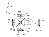
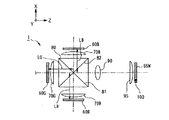
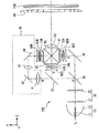
まず、本発明の第1の実施形態に係る投射型表示装置1の構成を図1〜図3に基づき説明する。図1は、本発明に係る投射型表示装置1の主たる光学構成を示す図であり、図2はダイクロイックプリズム80の構成を示す図であり、図3は、光学像を等倍で伝達するリレー光学系の一例を示す図である。
First, the structure of the projection
投射型表示装置1は、図1に示すように、光源10と、インテグレータ20と、ダイクロイックミラー30,35と、反射ミラー36と、リレー光学系40と、平行化レンズ50B,50G,50Rと、液晶ライトバルブ60B,60G,60Rと、入射側レンズ70B,70G,70Rと、光合成用クロスダイクロイックプリズム80と、リレーレンズ90と、射出側レンズ95と、液晶ライトバルブ100と、投射レンズ110と、を含んだ構成となっている。
As shown in FIG. 1, the
光源10は、超高圧水銀ランプやキセノンランプ等から成る光源ランプ11と、光源からの光を集光するリフレクタ12と、から構成されている。
The
インテグレータ20は、フライアイレンズ等から成る第1レンズアレイ21及び第2レンズアレイ22から構成されており、光源10の輝度むらを分散し、照射面で一様な照度分布を得るためのものである。
The
ダイクロイックミラー30は、ガラス板等に青色光及び緑色光を反射し、赤色光を透過する性質のダイクロイック膜を形成したもので、光源10からの白色光に対して、当該白色光に含まれる青色光及び緑色光を反射し、赤色光を透過する。
The
ダイクロイックミラー35は、ガラス板等に緑色光を反射し、青色光を透過する性質のダイクロイック膜を形成したもので、ダイクロイックミラー30を透過した緑色光及び青色光のうち、緑色光を反射して平行化レンズ50Gに伝達し、青色光を透過してリレー光学系40に伝達する。
The
反射ミラー36は、ダイクロイックミラー30を透過した赤色光を反射して平行化レンズ50Rに伝達する。
The
リレー光学系40は、入射側レンズ41と、リレーレンズ42と、反射ミラー45,46と、から構成されている。
The relay
リレーレンズ42は入射側レンズ41近傍の光(光強度分布)を平行化レンズ50B近傍に伝達するもので、入射側レンズ41はリレーレンズ42に光を効率よく入射させる機能を有する。このリレー光学系40によって入射側レンズ41に入射した青色光はその強度分布をほぼ保存された状態で、かつ光損失を殆ど伴うことなく空間的に離れた液晶ライトバルブ60Bに伝達される。
The
平行化レンズ50Bは、反射ミラー46によって伝達された青色光を略平行化して液晶ライトバルブ60Bに向けて射出する。
The
平行化レンズ50Gは、ダイクロイックミラー35によって伝達された緑色光を略平行化して液晶ライトバルブ60Gに向けて射出する。
The
平行化レンズ50Rは、反射ミラー36によって伝達された赤色光を略平行化して液晶ライトバルブ60Rに向けて射出する。
The
上記3つの平行化レンズ50B,50G,50Rは対応する液晶ライトバルブ50B,50G,50Rに入射する各色光を略平行化して入射光の角度分布を狭め、液晶ライトバルブ50B,50G,50Rの表示特性を向上させる機能を有している。
The three
液晶ライトバルブ60Bは、透過率を独立に制御可能な複数の画素をマトリクス状に配列した構成を有したもので、平行化レンズ50Bによって略平行化されて入射された青色光を表示画像データに基づいて光変調し、光学像を内包した変調光を射出する。
The liquid crystal
液晶ライトバルブ60Gは、透過率を独立に制御可能な複数の画素をマトリクス状に配列した構成を有したもので、平行化レンズ50Gによって略平行化されて入射された緑色光を表示画像データに基づいて光変調し、光学像を内包した変調光を射出する。
The liquid crystal
液晶ライトバルブ60Rは、透過率を独立に制御可能な複数の画素をマトリクス状に配列した構成を有したもので、平行化レンズ50Rによって略平行化されて入射された赤色光を表示画像データに基づいて光変調し、光学像を内包した変調光を射出する。
The liquid crystal
入射側レンズ70B,70G,70Rは、対応する各液晶ライトバルブ60B,60G,60Rによって変調された各色の変調光をリレーレンズ90に効率よく入射させる機能を有するもので、各々の変調光を集光し光合成用クロスダイクロイックプリズム80を経てリレーレンズ90に入射させる。
The
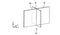
光合成用クロスダイクロイックプリズム80は、図2に示すように、三角柱形状の4つのプリズムを接合して成る6面体形状を有しており、内部に青光反射ダイクロイック膜81と赤光反射ダイクロイック膜82が断面X字状に配置されている。入射した青色光及び赤色光を対応するダイクロイック膜でリレーレンズ90側に反射し、一方、入射した緑色光をリレーレンズ90側にそのまま透過することにより、RGBの3原色の光を合成してリレーレンズ90側に射出する。ここで、光学収差を低減するために、光伝達過程内に配置する光合成用クロスダイクロイックプリズム80を分散性の少ない光学材料(例えば、ゼロ分散あるいは低分散ガラス等)で形成するのが好ましい。
As shown in FIG. 2, the photosynthesis cross
リレーレンズ90は、3ヶ所の液晶ライトバルブ60B、60G,60Rの表示面上に形成された3つの光学像(光強度分布)を途中の光合成用クロスダイクロイックプリズム80で合成しながら射出側レンズ95を経て、後述する液晶ライトバルブ100の表示面上にその強度分布をほぼ保存した状態で、かつ光損失を殆ど伴うことなく正確に伝達する機能を有するもので、光合成用クロスダイクロイックプリズム80からの合成光を射出側レンズ95に向けて射出する。
The
射出側レンズ95は、リレーレンズ90によって導かれた合成光を略平行化して液晶ライトバルブ100に向けて射出する。射出側レンズ95の後段に配置された液晶ライトバルブ100や投射レンズ110がその表示特性に光の入射角依存性を有するため、それらの光学素子に対して入射する光の角度分布の広がりを抑えて、表示性能や光利用効率を向上させる目的で射出側レンズ95は配置される。したがって、射出側レンズ95以降の光学素子によっては、射出側レンズ95を省いても良い。
The
液晶ライトバルブ100は、透過率を独立に制御可能な複数の画素をマトリクス状に配列した構成を有したもので、射出側レンズ95からの全波長領域に及ぶ合成光を表示画像データに基づいて光変調し、最終的な光学像を内包した変調光を射出する。
The liquid crystal
投射レンズ110は、液晶ライトバルブ100の表示面上に形成された光学像を図示しないスクリーン上に投射してカラー画像を表示する。
The
ここで、液晶ライトバルブ60B,60G,60R,100は、画素電極およびこれを駆動するための薄膜トランジスタ素子や薄膜ダイオード等のスイッチング素子がマトリクス状に形成されたガラス基板と、全面にわたって共通電極が形成されたガラス基板と、それらの間に挟持されたTN型液晶を有し、外面の両側に偏光板を配置したアクティブマトリックス型の液晶表示素子である。制御値(印加電圧)に応じて透過率を変え、液晶ライトバルブを通過する光の強度を変調することができる。例えば、電圧非印加状態で白/明(透過)状態、電圧印加状態で黒/暗(非透過)状態となり、与えられた制御値(印加電圧)に応じてその間の階調がアナログ的に制御される。液晶ライトバルブ60B,60G,60R及び液晶ライトバルブ100は何れも透過光の強度を変調し、その変調度合いに応じた光学像を内包する点では同じであるが、後者の液晶ライトバルブ100は全波長域の光(白色光)を変調するのに対して、前者の液晶ライトバルブ60B,60G,60Rは光分離手段であるダイクロイックミラー30,35で分光された特定波長領域の光(R,G,Bなどの色光)を変調する点で両者は異なっている。したがって、以下では液晶ライトバルブ60B,60G,60Rで行われる光強度変調を色変調、液晶ライトバルブ100で行われる光強度変調を輝度変調と便宜的に呼称して区別する。また、同様の観点から、液晶ライトバルブ60B,60G,60Rを色変調ライトバルブ、液晶ライトバルブ100を輝度変調ライトバルブと呼称して区別する場合がある。そして、色変調ライトバルブ及び輝度変調ライトバルブに入力する制御データの内容については後ほど詳述する。なお、本実施形態では、色変調ライトバルブは輝度変調ライトバルブよりも高い解像度を有し、よって、色変調ライトバルブが表示解像度(投射型表示装置1の表示画像を観測者が見たときに観測者が知覚する解像度をいう。)を決定する場合を想定している。勿論、表示解像度の関係はこれに限定されず、輝度変調ライトバルブが表示解像度を決定する構成も可能である。
Here, in the liquid crystal
次に、投射型表示装置1の全体的な光伝達の流れを説明する。光源10からの白色光はダイクロイックミラー30,35により赤色(R)、緑色(G)および青色(B)の3原色光に分光されるとともに、平行化レンズ50R,50G、リレー光学系40、平行化レンズ50Bを介して、液晶ライトバルブ60B,60G、60R(色変調ライトバルブ)に入射される。液晶ライトバルブ60B,60G,60Rに入射した各々の色光はそれぞれの波長領域に応じた外部データに基づいて色変調され、光学像を内包した変調光として射出される。液晶ライトバルブ60B,60G、60Rからの各変調光は、それぞれ入射側レンズ70B,70G,70Rを介してダイクロイックプリズム80に入射し、そこで一つの光に合成され、リレーレンズ90及び射出側レンズ95を介してライトバルブ100に入射される。液晶ライトバルブ100に入射した合成光は全波長域に応じた外部データに基づいて輝度変調され、最終的な光学像を内包した変調光として投射部110へ射出される。そして、投射部110において、液晶ライトバルブ100からの最終的な合成光を図示しないスクリーン上に投射し所望の画像を表示する。
Next, the overall light transmission flow of the
投射型表示装置1では、第1光変調素子である液晶ライトバルブ60B,60G、60Rで光学像(画像)を形成した変調光を用いて、最終的な表示画像を第2光変調素子である液晶ライトバルブ100で形成する形態を採用しており、この2段階の画像形成過程によって階調表現性に優れた(高い輝度ダイナミックレンジを有する)表示画像の形成を実現している。したがって、液晶ライトバルブ60B,60G、60Rで形成した光学像(画像)を液晶ライトバルブ100上に正確且つ高い効率で伝達する必要がある。そのためには、入射側レンズ70B,70G,70R、リレーレンズ90及び射出側レンズ95を含んで構成される光伝達系に、アクロマートレンズや非球面レンズを追加したり、或いは、入射側レンズ70B,70G,70R、リレーレンズ90及び射出側レンズ95として、アクロマートレンズや非球面レンズを適用することが効果的である。さらには、入射側レンズ70B,70G,70Rの材質やレンズ曲率などの光学特性などを個別に最適化しても良い。この様な構成を採用することにより、光学像(画像)伝達過程における光学収差の発生を抑制でき、正確且つ高い効率での光学像(光強度分布)伝達を実現することができる。
In the
なお、液晶ライトバルブ60B,60G、60R及び液晶ライトバルブ100の解像度及び寸法を互いに同一とした場合には、入射側レンズ70B,70G,70R、リレーレンズ90及び射出側レンズ95によって構成されるリレー光学系を、等倍のリレー光学系にすれば良い。等倍のリレー光学系とした場合に、図3に示すように、液晶ライトバルブ60B,60G、60R上に形成された光学像は、反転しつつも大きさを変えずに(等倍倒立像として)正確に液晶ライトバルブ100に伝達される。なお、上記リレー光学系は、両側テレセントリック性を有するのが好ましい。
When the resolution and dimensions of the liquid crystal
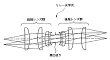
ここで、図4は、両側テレセントリック性を有するリレー光学系の構成例を示す図である。
リレー光学系は、図4に示すように、開口絞りに対してほぼ対称に配置された前段レンズ群および後段レンズ群からなる等倍結像レンズ系である。前段レンズ群および後段レンズ群は、複数の凸レンズと、1枚の凹レンズとで構成されている。ただし、レンズの形状、大きさ、配置間隔および枚数、テレセントリック性、倍率その他のレンズ特性は、要求される特性によって適宜変更され得るものであり、図4の例に限定されるものではない。
Here, FIG. 4 is a diagram illustrating a configuration example of a relay optical system having both-side telecentricity.
As shown in FIG. 4, the relay optical system is an equal-magnification imaging lens system that includes a front lens group and a rear lens group that are arranged almost symmetrically with respect to the aperture stop. The front lens group and the rear lens group are configured by a plurality of convex lenses and one concave lens. However, the lens shape, size, arrangement interval and number, telecentricity, magnification, and other lens characteristics can be appropriately changed according to required characteristics, and are not limited to the example of FIG.
図5は、図4のリレー光学系の動作原理を示す図である。
リレー光学系は、図5に示すように、典型的には等倍結像のものが用いられるので、液晶ライトバルブ60B,60G、60Rおよび液晶ライトバルブ100の画素密度を同一としても、液晶ライトバルブ60B,60G、60Rの画素と液晶ライトバルブ100の画素を1対1に対応させることができる。また、リレー光学系は、多数枚のレンズから構成されるので、収差補正が良く、液晶ライトバルブ60B,60G、60Rで形成される輝度分布を正確に液晶ライトバルブ100に伝達することができる。
FIG. 5 is a diagram showing the operating principle of the relay optical system of FIG.
As shown in FIG. 5, the relay optical system typically has an equal magnification image formation. Therefore, even if the liquid crystal
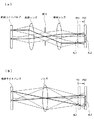
図6及び図7は、テレセントリック性の説明図であり、図6(a)、図7(a)は両側テレセントリック性を有するリレー光学系を示し、図6(b)、図7(b)は一般的なリレー光学系を示している。 FIGS. 6 and 7 are explanatory diagrams of telecentricity. FIGS. 6A and 7A show a relay optical system having both-side telecentricity. FIGS. 6B and 7B are diagrams. A general relay optical system is shown.
テレセントリック光学系とは、図6(a)に示すように、太い実線で示す主光線が物体側(前段ライトバルブ側)空間もしくは像側(後段ライトバルブ側)空間において光軸に対して平行な光学系であり、物体側(前段ライトバルブ側)及び像側(後段ライトバルブ側)のいずれの側にもテレセントリックなものを両側テレセントリック光学系という。両側テレセントリック性を有するリレー光学系では、前段ライトバルブ(本例では液晶ライトバルブ)から出射する主光線は前段ライトバルブのいずれの部位からもほぼ垂直に出射し、後段ライトバルブ(本例では液晶ライトバルブ)にほぼ垂直に入射する。したがって、前段ライトバルブの光軸から遠い位置(A)から出射する光束の出射角度分布と、光軸から近い位置(B)から出射する光束の出射角度分布とを比較した場合、それらはほぼ等しい。 In the telecentric optical system, as shown in FIG. 6A, a chief ray indicated by a thick solid line is parallel to the optical axis in the object side (front light valve side) space or the image side (rear light valve side) space. An optical system that is telecentric on either the object side (front light valve side) or the image side (rear light valve side) is called a double-sided telecentric optical system. In a relay optical system that has telecentricity on both sides, the principal ray emitted from the front light valve (in this example, the liquid crystal light valve) is emitted almost vertically from any part of the front light valve, and the rear light valve (in this example, the liquid crystal light valve). Light enters the light valve almost perpendicularly. Therefore, when the emission angle distribution of the light beam emitted from the position (A) far from the optical axis of the front light valve is compared with the emission angle distribution of the light beam emitted from the position (B) close to the optical axis, they are substantially equal. .
一方、図6(b)に示すように、一般的なリレー光学系では、太い実線で示す主光線は、前段ライトバルブの出射位置によって出射角度が異なり、後段ライトバルブへの入射角も入射位置によって異なる。したがって、前段ライトバルブの光軸から遠い位置(A)から出射する光束の出射角度分布と、光軸から近い位置(B)から出射する光束の出射角度分布とを比較した場合、それらはかなり異なる。 On the other hand, as shown in FIG. 6B, in a general relay optical system, the chief ray indicated by a thick solid line has an emission angle different depending on the emission position of the front light valve, and the incident angle to the rear light valve is also the incident position. It depends on. Therefore, when the emission angle distribution of the light beam emitted from the position (A) far from the optical axis of the front light valve is compared with the emission angle distribution of the light beam emitted from the position (B) close to the optical axis, they are quite different. .
ところで、一般に、液晶ライトバルブは視角依存性を有する。すなわち、液晶ライトバルブから出射する光線の角度によって、コントラスト特性、明るさの特性、分光特性等が異なる。したがって、図6(b)に示す一般的なリレー光学系では、前段ライトバルブ(液晶ライトバルブ)の領域ごとに出射光束の出射角度成分が異なり、その結果、後段ライトバルブ(液晶ライトバルブ)の画面内で、表示画像の明るさ、色味、コントラストに分布(不均一性)が生じ、プロジェクタの画像表示品質の低下を招く可能性がある。 By the way, in general, a liquid crystal light valve has a viewing angle dependency. That is, contrast characteristics, brightness characteristics, spectral characteristics, and the like differ depending on the angle of light emitted from the liquid crystal light valve. Therefore, in the general relay optical system shown in FIG. 6B, the emission angle component of the emitted light beam differs for each region of the front light valve (liquid crystal light valve), and as a result, the rear light valve (liquid crystal light valve) Distribution (non-uniformity) occurs in the brightness, color, and contrast of the display image in the screen, which may cause a reduction in the image display quality of the projector.
これに対して、図6(a)に示す両側テレセントリック性を有するリレー光学系では、前段ライトバルブ(液晶ライトバルブ)のどの領域の出射光束もほぼ同じ出射角度分布であるため、後段ライトバルブ(液晶ライトバルブ)の画面内における表示画像の明るさ、色味、コントラストが略均一であり、プロジェクタの画像表示品質が良好である。 On the other hand, in the relay optical system having both-side telecentricity shown in FIG. 6 (a), the luminous flux in any region of the front light valve (liquid crystal light valve) has substantially the same outgoing angle distribution. The brightness, color and contrast of the display image in the screen of the liquid crystal light valve) are substantially uniform, and the image display quality of the projector is good.
さらに、図7(a)に示すように、両側テレセントリック性を有するリレー光学系では、後段ライトバルブの光軸方向の配置位置に誤差が生じても(図7(a)に示す、PS1→PS2)、主光線が光軸に対して平行なので、前段ライトバルブの像は多少ボケが生じるものの大きさはほとんど変わらない(図7(a)に示す、AL1≒AL2)。すなわち、後段ライトバルブの配置誤差が多少あっても、プロジェクタとしての画像表示品質はあまり低下しないので、製造マージンが大きい。 Further, as shown in FIG. 7 (a), in the relay optical system having both-side telecentricity, even if an error occurs in the arrangement position of the rear light valve in the optical axis direction (PS1 → PS2 shown in FIG. 7 (a)). ) Since the principal ray is parallel to the optical axis, the image of the front light valve is slightly blurred but the size is almost unchanged (AL1≈AL2 shown in FIG. 7A). That is, even if there is a slight arrangement error of the rear light valve, the image display quality as a projector does not deteriorate so much, and the manufacturing margin is large.
一方、図7(b)に示すように、一般的なリレー光学系では、後段ライトバルブに上記と同等の配置誤差があった場合(図7(b)に示す、PS1→PS2)、主光線が光軸に対して非平行なので、前段ライトバルブの像にボケと同時に大きさの変化が生じ(図7(b)に示す、AL1<AL2)、結果として画像表示品質が大きく低下する可能性がある。 On the other hand, as shown in FIG. 7B, in a general relay optical system, when the rear light valve has an arrangement error equivalent to the above (PS1 → PS2 shown in FIG. 7B), the chief ray Is not parallel to the optical axis, the image of the preceding light valve changes in size simultaneously with the blur (AL1 <AL2 shown in FIG. 7B), and as a result, the image display quality may be greatly reduced. There is.
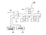
次に、表示制御装置200の構成を図8〜図12に基づき詳細に説明する。
Next, the configuration of the
図8は、表示制御装置200のハードウェア構成を示すブロック図である。
FIG. 8 is a block diagram illustrating a hardware configuration of the
表示制御装置200は、図8に示すように、制御プログラムに基づいて演算およびシステム全体を制御するCPU170と、所定領域にあらかじめCPU170の制御プログラム等を格納しているROM172と、ROM172等から読み出したデータやCPU170の演算過程で必要な演算結果を格納するためのRAM174と、外部装置に対してデータの入出力を媒介するI/F178とで構成されており、これらは、データを転送するための信号線であるバス179で相互にかつデータ授受可能に接続されている。
As shown in FIG. 8, the
I/F178には、外部装置として、輝度変調ライトバルブ(液晶ライトバルブ100)および色変調ライトバルブ(液晶ライトバルブ60B,60G、60R)を駆動するライトバルブ駆動装置180と、データやテーブル等をファイルとして格納する記憶装置182と、外部のネットワーク199に接続するための信号線とが接続されている。
The I /
記憶装置182は、輝度変調ライトバルブおよび色変調ライトバルブを駆動するためのHDR表示データを記憶している。
The
HDR表示データは、従来のsRGB等の画像フォーマットでは実現できない高い輝度ダイナミックレンジを実現することができる画像データであり、画素の輝度レベルを示す画素値を画像の全画素について格納している。本実施形態では、HDR表示データとして、1つの画素についてRGB3原色ごとに輝度レベルを示す画素値を浮動小数点値として格納した形式を用いる。例えば、1つの画素の画素値として(1.2,5.4,2.3)という値が格納されている。 The HDR display data is image data capable of realizing a high luminance dynamic range that cannot be realized by a conventional image format such as sRGB, and stores pixel values indicating pixel luminance levels for all pixels of the image. In the present embodiment, the HDR display data uses a format in which a pixel value indicating a luminance level for each of the three RGB primary colors is stored as a floating point value for one pixel. For example, the value (1.2, 5.4, 2.3) is stored as the pixel value of one pixel.
ここで、HDR表示データにおける画素pの輝度レベルをRp、第2光変調素子の画素pに対応する画素の透過率をT1、第1光変調素子の画素pに対応する画素の透過率をT2とすると、下式(1),(2)が成立する。
Rp = Tp×Rs …(1)
Tp = T1×T2×G …(2)
ただし、上式(1),(2)において、Rsは光源の輝度、Gはゲインであり、いずれも定数である。また、Tpは、光変調率である。
Here, the luminance level of the pixel p in the HDR display data is Rp, the transmittance of the pixel corresponding to the pixel p of the second light modulation element is T1, and the transmittance of the pixel corresponding to the pixel p of the first light modulation element is T2. Then, the following expressions (1) and (2) are established.
Rp = Tp × Rs (1)
Tp = T1 × T2 × G (2)
However, in the above formulas (1) and (2), Rs is the luminance of the light source, G is the gain, and both are constants. Tp is a light modulation rate.
なお、HDR表示データの生成方法の詳細については、例えば、公知文献1「P.E.Debevec, J.Malik, "Recovering High Dynamic Range Radiance Maps from Photographs", Proceedings of ACM SIGGRAPH97 , pp.367-378 (1997)」に掲載されている。
For details of the method for generating HDR display data, see, for example, publicly known
また、記憶装置182は、輝度変調ライトバルブの制御値を登録した制御値登録テーブル400を記憶している。
Further, the
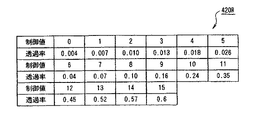
図9は、制御値登録テーブル400のデータ構造を示す図である。 FIG. 9 is a diagram illustrating a data structure of the control value registration table 400.
制御値登録テーブル400には、図9に示すように、輝度変調ライトバルブの各制御値ごとに1つのレコードが登録されている。各レコードは、輝度変調ライトバルブの制御値を登録したフィールドと、輝度変調ライトバルブの透過率を登録したフィールドとを含んで構成されている。 In the control value registration table 400, as shown in FIG. 9, one record is registered for each control value of the luminance modulation light valve. Each record includes a field in which the control value of the luminance modulation light valve is registered and a field in which the transmittance of the luminance modulation light valve is registered.
図9の例では、第1段目のレコードには、制御値として「0」が、透過率として「0.003」がそれぞれ登録されている。これは、輝度変調ライトバルブに対して制御値「0」を出力すると、輝度変調ライトバルブの透過率が0.3%となることを示している。なお、図9は、輝度変調ライトバルブの階調数が4ビット(0〜15値)である場合の例を示したが、実際には、輝度変調ライトバルブの階調数に相当するレコードが登録される。例えば、階調数が8ビットである場合は、256個のレコードが登録される。 In the example of FIG. 9, “0” is registered as the control value and “0.003” is registered as the transmittance in the first row record. This indicates that when the control value “0” is output to the luminance modulation light valve, the transmittance of the luminance modulation light valve is 0.3%. Note that FIG. 9 shows an example in which the number of gradations of the luminance modulation light valve is 4 bits (0 to 15 values). However, in reality, there is a record corresponding to the number of gradations of the luminance modulation light valve. be registered. For example, when the number of gradations is 8 bits, 256 records are registered.
また、記憶装置182は、各色変調ライトバルブごとに、その色変調ライトバルブの制御値を登録した制御値登録テーブルを記憶している。
Further, the
図9は、液晶ライトバルブ60Rの制御値を登録した制御値登録テーブル420Rのデータ構造を示す図である。
FIG. 9 is a diagram illustrating a data structure of a control value registration table 420R in which control values of the liquid crystal
制御値登録テーブル420Rには、図10に示すように、液晶ライトバルブ60Rの各制御値ごとに1つのレコードが登録されている。各レコードは、液晶ライトバルブ60Rの制御値を登録したフィールドと、液晶ライトバルブ60Rの透過率を登録したフィールドとを含んで構成されている。
In the control value registration table 420R, as shown in FIG. 10, one record is registered for each control value of the liquid crystal
図10の例では、第1段目のレコードには、制御値として「0」が、透過率として「0.004」がそれぞれ登録されている。これは、液晶ライトバルブ60Rに対して制御値「0」を出力すると、液晶ライトバルブ60Rの透過率が0.4%となることを示している。なお、図10は、色変調ライトバルブの階調数が4ビット(0〜15値)である場合の例を示したが、実際には、色変調ライトバルブの階調数に相当するレコードが登録される。例えば、階調数が8ビットである場合は、256個のレコードが登録される。
In the example of FIG. 10, “0” is registered as the control value and “0.004” is registered as the transmittance in the first-stage record. This indicates that when the control value “0” is output to the liquid crystal
また、液晶ライトバルブ60B,60Gに対応する制御値登録テーブルのデータ構造については特に図示しないが、制御値登録テーブル420Rと同様のデータ構造を有している。ただし、同一の制御値に対して異なる透過率が登録されている点が制御値登録テーブル420Rと異なる。
The data structure of the control value registration table corresponding to the liquid crystal
次に、CPU170の構成およびCPU170で実行される処理を説明する。
Next, the configuration of the
CPU170は、マイクロプロセッシングユニット(MPU)等からなり、ROM172の所定領域に格納されている所定のプログラムを起動させ、そのプログラムに従って、図11のフローチャートに示す表示制御処理を実行するようになっている。
The
図11は、表示制御処理を示すフローチャートである。 FIG. 11 is a flowchart showing the display control process.
表示制御処理は、HDR表示データに基づいて輝度変調ライトバルブおよび色変調ライトバルブの制御値をそれぞれ決定し、決定した制御値に基づいて輝度変調ライトバルブおよび色変調ライトバルブを駆動する処理であって、CPU170において実行されると、図11に示すように、まず、ステップS100に移行するようになっている。
The display control process is a process of determining the control values of the luminance modulation light valve and the color modulation light valve based on the HDR display data, and driving the luminance modulation light valve and the color modulation light valve based on the determined control value. When executed in the
ステップS100では、HDR表示データを記憶装置182から読み出す。
In step S100, the HDR display data is read from the
次いで、ステップS102に移行して、読み出したHDR表示データを解析し、画素値のヒストグラムや、輝度レベルの最大値、最小値および平均値等を算出する。この解析結果は、暗めのシーンを明るくしたり、明るすぎるシーンを暗くしたり、中間部コントラストを協調するなどの自動画像補正に使用したり、トーンマッピングに使用したりするためである。 In step S102, the read HDR display data is analyzed, and a histogram of pixel values, a maximum value, a minimum value, an average value, and the like of the luminance level are calculated. This analysis result is for use in automatic image correction such as brightening a dark scene, darkening a scene that is too bright, or coordinating intermediate contrast, or for tone mapping.
次いで、ステップS104に移行して、ステップS102の解析結果に基づいて、HDR表示データの輝度レベルを投射型表示装置1の輝度ダイナミックレンジにトーンマッピングする。
Next, the process proceeds to step S104, and the luminance level of the HDR display data is tone-mapped to the luminance dynamic range of the
図12は、トーンマッピング処理を説明するための図である。 FIG. 12 is a diagram for explaining tone mapping processing.
HDR表示データを解析した結果、HDR表示データに含まれる輝度レベルの最小値がSminで、最大値がSmaxであるとする。また、投射型表示装置1の輝度ダイナミックレンジの最小値がDminで、最大値がDmaxであるとする。図12の例では、SminがDminよりも小さく、SmaxがDmaxよりも大きいので、このままでは、HDR表示データを適切に表示することができない。そこで、Smin〜SmaxのヒストグラムがDmin〜Dmaxのレンジに収まるように正規化する。
As a result of analyzing the HDR display data, it is assumed that the minimum value of the luminance level included in the HDR display data is Smin and the maximum value is Smax. Further, it is assumed that the minimum value of the luminance dynamic range of the
なお、トーンマッピングの詳細については、例えば、公知文献2「F.Drago, K.Myszkowski, T.Annen, N.Chiba, "Adaptive Logarithmic Mapping For Displaying High Contrast Scenes", Eurographics 2003, (2003)」に掲載されている。
Details of tone mapping are described in, for example, publicly known
次いで、ステップS106に移行して、色変調ライトバルブの解像度に合わせてHDR画像をリサイズ(拡大または縮小)する。このとき、HDR画像のアスペクト比を保持したままHDR画像をリサイズする。リサイズ方法としては、例えば、平均値法、中間値法、ニアレストネイバー法(最近傍法)が挙げられる。 Next, the process proceeds to step S106, and the HDR image is resized (enlarged or reduced) in accordance with the resolution of the color modulation light valve. At this time, the HDR image is resized while maintaining the aspect ratio of the HDR image. Examples of the resizing method include an average value method, an intermediate value method, and a nearest neighbor method (nearest neighbor method).
次いで、ステップS108に移行して、リサイズ画像の画素の輝度レベルRpおよび光源10の輝度Rsに基づいて、上式(1)により、リサイズ画像の各画素ごとに光変調率Tpを算出する。
Next, the process proceeds to step S108, and the light modulation rate Tp is calculated for each pixel of the resized image by the above equation (1) based on the luminance level Rp of the pixel of the resized image and the luminance Rs of the
次いで、ステップS110に移行して、色変調ライトバルブの各画素の透過率T2として初期値(例えば、0.2)を与え、色変調ライトバルブの各画素の透過率T2を仮決定する。 Next, the process proceeds to step S110, where an initial value (for example, 0.2) is given as the transmittance T2 of each pixel of the color modulation light valve, and the transmittance T2 of each pixel of the color modulation light valve is provisionally determined.
次いで、ステップS112に移行して、算出した光変調率Tp、仮決定した透過率T2およびゲインGに基づいて、上式(2)により、色変調ライトバルブの画素単位で輝度変調ライトバルブの透過率T1'を算出する。ここで、色変調ライトバルブが3枚の液晶ライトバルブ60B,60G,60Rから構成されていることから、同一の画素についてRGB3原色ごとに透過率T1'が算出される。これに対し、輝度変調ライトバルブが1枚の液晶ライトバルブ100から構成されていることから、それらの平均値等をその画素のT1'として算出する。
Next, the process proceeds to step S112, and based on the calculated light modulation rate Tp, the provisionally determined transmittance T2 and the gain G, the transmission of the luminance modulation light valve in units of pixels of the color modulation light valve according to the above equation (2). The rate T1 ′ is calculated. Here, since the color modulation light valve is composed of the three liquid crystal
次いで、ステップS114に移行して、輝度変調ライトバルブの画素ごとに、その画素と光路上で重なり合う色変調ライトバルブの画素について算出した透過率T1'の重み付け平均値をその画素の透過率T1として算出する。重み付けは、重なり合う画素の面積比により行う。 Next, the process proceeds to step S114, and for each pixel of the luminance modulation light valve, the weighted average value of the transmittance T1 ′ calculated for the pixel of the color modulation light valve that overlaps the pixel on the optical path is set as the transmittance T1 of the pixel. calculate. Weighting is performed based on the area ratio of overlapping pixels.
次いで、ステップS116に移行して、輝度変調ライトバルブの画素ごとに、その画素について算出した透過率T1に対応する制御値を制御値登録テーブル400から読み出し、読み出した制御値をその画素の制御値として決定する。制御値の読出では、算出した透過率T1に最も近似する透過率を制御値登録テーブル400の中から検索し、検索により索出した透過率に対応する制御値を読み出す。この検索は、例えば、2分探索法を用いて行うことにより高速な検索を実現する。 Next, the process proceeds to step S116, and for each pixel of the luminance modulation light valve, a control value corresponding to the transmittance T1 calculated for the pixel is read from the control value registration table 400, and the read control value is the control value of the pixel. Determine as. In the reading of the control value, the transmittance that most closely approximates the calculated transmittance T1 is searched from the control value registration table 400, and the control value corresponding to the transmittance found by the search is read. This search is performed using, for example, a binary search method, thereby realizing a high-speed search.
次いで、ステップS118に移行して、色変調ライトバルブの画素ごとに、その画素と光路上で重なり合う輝度変調ライトバルブの画素について決定した透過率T1の重み付け平均値を算出し、算出した平均値、ステップS108で算出した光変調率TpおよびゲインGに基づいて、上式(2)により、その画素の透過率T2を算出する。重み付けは、重なり合う画素の面積比により行う。 Next, the process proceeds to step S118, and for each pixel of the color modulation light valve, a weighted average value of the transmittance T1 determined for the pixel of the luminance modulation light valve overlapping with the pixel on the optical path is calculated, and the calculated average value, Based on the light modulation rate Tp and gain G calculated in step S108, the transmittance T2 of the pixel is calculated by the above equation (2). Weighting is performed based on the area ratio of overlapping pixels.
次いで、ステップS120に移行して、色変調ライトバルブの画素ごとに、その画素について算出した透過率T2に対応する制御値を制御値登録テーブルから読み出し、読み出した制御値をその画素の制御値として決定する。制御値の読出では、算出した透過率T2に最も近似する透過率を制御値登録テーブルの中から検索し、検索により索出した透過率に対応する制御値を読み出す。この検索は、例えば、2分探索法を用いて行うことにより高速な検索を実現する。 Next, the process proceeds to step S120, and for each pixel of the color modulation light valve, a control value corresponding to the transmittance T2 calculated for that pixel is read from the control value registration table, and the read control value is used as the control value for that pixel. decide. In the reading of the control value, the transmittance that most closely approximates the calculated transmittance T2 is searched from the control value registration table, and the control value corresponding to the transmittance found by the search is read. This search is performed using, for example, a binary search method, thereby realizing a high-speed search.
次いで、ステップS122に移行して、ステップS116,S120で決定した制御値をライトバルブ駆動装置180に出力し、色変調ライトバルブおよび輝度変調ライトバルブをそれぞれ駆動して表示画像を投影し、一連の処理を終了して元の処理に復帰させる。
Next, the process proceeds to step S122, the control values determined in steps S116 and S120 are output to the light
次に、色変調ライトバルブ(液晶ライトバルブ60B,60G、60R)及び輝度変調ライトバルブ(液晶ライトバルブ100)に書き込む画像データの生成過程を図13〜図16に基づき説明する。
Next, a process of generating image data to be written in the color modulation light valve (liquid crystal
以下では、色変調ライトバルブ(液晶ライトバルブ60B,60G、60R)はいずれも、横18画素×縦12画素の解像度および4ビットの階調数を有し、輝度変調ライトバルブ(液晶ライトバルブ100)は、横15画素×縦10画素の解像度および4ビットの階調数を有する場合を例にとって説明を行う。
In the following, all of the color modulation light valves (liquid crystal
表示制御装置200では、ステップS100〜S104を経て、HDR表示データが読み出され、読み出されたHDR表示データが解析され、その解析結果に基づいて、HDR表示データの輝度レベルが投射型表示装置1の輝度ダイナミックレンジにトーンマッピングされる。次いで、ステップS106を経て、色変調ライトバルブの解像度に合わせてHDR画像がリサイズされる。
In the
次いで、ステップS108を経て、リサイズ画像の画素ごとに光変調率Tpが算出される。例えば、リサイズ画像における画素pの光変調率Tpは、画素pの輝度レベルRp(R,G,B)が(1.2,5.4,2.3)、光源10の輝度Rs(R,G,B)が(10000,10000,10000)であるとすると、(1.2,5.4,2.3)/(10000,10000,10000)=(0.00012,0.00054,0.00023)となる。 Next, through step S108, the light modulation rate Tp is calculated for each pixel of the resized image. For example, the light modulation rate Tp of the pixel p in the resized image is such that the luminance level Rp (R, G, B) of the pixel p is (1.2, 5.4, 2.3) and the luminance Rs (R, R, If (G, B) is (10000, 10000, 10000), then (1.2, 5.4, 2.3) / (10000, 10000, 10000) = (0.00012, 0.00054, 0.00023).
図13は、色変調ライトバルブの透過率T2を仮決定する場合を示す図である。 FIG. 13 is a diagram illustrating a case where the transmittance T2 of the color modulation light valve is provisionally determined.
次いで、ステップS110を経て、色変調ライトバルブの各画素の透過率T2が仮決定される。色変調ライトバルブの左上4区画の画素をp21(左上)、p22(右上)、p23(左下)、p24(右下)とした場合、画素p21〜p24の透過率T2には、図13に示すように、初期値T20が与えられる。 Next, through step S110, the transmittance T2 of each pixel of the color modulation light valve is provisionally determined. When the pixels in the upper left four sections of the color modulation light valve are p21 (upper left), p22 (upper right), p23 (lower left), and p24 (lower right), the transmittance T2 of the pixels p21 to p24 is shown in FIG. Thus, an initial value T20 is given.
図14は、色変調ライトバルブの画素単位で輝度変調ライトバルブの透過率T1'を算出する場合を示す図である。 FIG. 14 is a diagram illustrating a case where the transmittance T1 ′ of the luminance modulation light valve is calculated for each pixel of the color modulation light valve.
次いで、ステップS112を経て、色変調ライトバルブの画素単位で輝度変調ライトバルブの透過率T1'が算出される。画素p21〜p24に着目した場合、これに対応する輝度変調ライトバルブの透過率T11〜T14は、図14に示すように、画素p21〜p24の光変調率をTp1〜Tp4、ゲインGを「1」とすると、下式(3)〜(6)により算出することができる。 Next, through step S112, the transmittance T1 ′ of the luminance modulation light valve is calculated for each pixel of the color modulation light valve. When attention is paid to the pixels p21 to p24, the transmittances T11 to T14 of the luminance modulation light valves corresponding thereto correspond to the light modulation rates of the pixels p21 to p24 as Tp1 to Tp4 and the gain G to “1” as shown in FIG. It can be calculated by the following formulas (3) to (6).
実際に数値を用いて計算する。Tp1=0.00012、Tp2=0.05、Tp3=0.02、Tp4=0.01、T20=0.1である場合は、下式(3)〜(6)によりT11=0.0012、T12=0.5、T13=0.2、T14=0.1となる。
T11 = Tp1/T20 …(3)
T12 = Tp2/T20 …(4)
T13 = Tp3/T20 …(5)
T14 = Tp4/T20 …(6)
図15は、輝度変調ライトバルブの各画素の透過率T1を決定する場合を示す図である。
Calculate using actual numerical values. When Tp1 = 0.00012, Tp2 = 0.05, Tp3 = 0.02, Tp4 = 0.01, and T20 = 0.1, T11 = 0.0012, T12 = 0.5, T13 = 0.2, and T14 = 0.1 according to the following equations (3) to (6). Become.
T11 = Tp1 / T20 (3)
T12 = Tp2 / T20 (4)
T13 = Tp3 / T20 (5)
T14 = Tp4 / T20 (6)
FIG. 15 is a diagram illustrating a case where the transmittance T1 of each pixel of the luminance modulation light valve is determined.
次いで、ステップS114を経て、輝度変調ライトバルブの各画素の透過率T1が決定される。色変調ライトバルブと輝度変調ライトバルブは、入射側レンズ70B,70G,70R、リレーレンズ90及び射出側レンズ95によって構成されるリレー光学系によって互いに倒立する関係にあるので、色変調パネル左上4区画の画素は輝度変調ライトバルブの右下部に結像される。輝度変調ライトバルブの右下4区画の画素をp11(右下)、p12(左下)、p13(右上)、p14(左上)とした場合、画素p11は、図15(a)に示すように、色変調ライトバルブと輝度変調ライトバルブの解像度が異なることから、画素p21〜画素p24と光路上で重なり合う。色変調ライトバルブの解像度が18×12で、輝度変調ライトバルブの解像度が15×10であるので、画素p11は、色変調ライトバルブの画素数の最小公倍数に基づいて6×6の矩形領域に区分することができる。そして、画素p11と画素p21〜p24との重なり合う面積比は、図15(b)に示すように、25:5:5:1となる。したがって、画素p11の透過率T15は、図15(c)に示すように、下式(7)により算出することができる。
Next, through step S114, the transmittance T1 of each pixel of the luminance modulation light valve is determined. The color modulation light valve and the luminance modulation light valve are in an inverted relationship with each other by the relay optical system constituted by the
実際に数値を用いて計算する。T11=0.0012、T12=0.5、T13=0.2、T14=0.002である場合は、下式(7)によりT15=0.1008となる。 Calculate using actual numerical values. When T11 = 0.0012, T12 = 0.5, T13 = 0.2, and T14 = 0.002, T15 = 0.008 according to the following equation (7).
T15=(T11×25+T12×5+T13×5+T14×1)/36 …(7)
画素p12〜p14の透過率T16〜T18についても、画素p11と同様に、面積比による重み付け平均値を算出することにより求めることができる。
T15 = (T11 × 25 + T12 × 5 + T13 × 5 + T14 × 1) / 36 (7)
Similarly to the pixel p11, the transmittances T16 to T18 of the pixels p12 to p14 can be obtained by calculating a weighted average value based on the area ratio.
次いで、ステップS116を経て、輝度変調ライトバルブの画素ごとに、その画素について算出された透過率T1に対応する制御値が制御値登録テーブル400から読み出され、読み出された制御値がその画素の制御値として決定される。例えば、T15=0.1008であるので、制御値登録テーブル400を参照すると、図9に示すように、0.09が最も近似した値となる。したがって、制御値登録テーブル400からは、画素p11の制御値として「8」が読み出される。 Next, through step S116, for each pixel of the luminance modulation light valve, a control value corresponding to the transmittance T1 calculated for the pixel is read from the control value registration table 400, and the read control value is the pixel. Is determined as a control value. For example, since T15 = 0.008, referring to the control value registration table 400, 0.09 is the closest value as shown in FIG. Therefore, “8” is read from the control value registration table 400 as the control value of the pixel p11.
図16は、色変調ライトバルブの各画素の透過率T2を決定する場合を示す図である。 FIG. 16 is a diagram illustrating a case where the transmittance T2 of each pixel of the color modulation light valve is determined.
次いで、ステップS118を経て、色変調ライトバルブの各画素の透過率T2が決定される。画素p24は、図16(a)に示すように、色変調ライトバルブと輝度変調ライトバルブの解像度が異なることから、画素p11〜画素p14と光路上で重なり合う。色変調ライトバルブの解像度が18×12で、輝度変調ライトバルブの解像度が15×10であるので、画素p24は、輝度変調ライトバルブの画素数の最小公倍数に基づいて5×5の矩形領域に区分することができる。そして、画素p24と画素p11〜p14との重なり合う面積比は、図16(b)に示すように、1:4:4:16となる。したがって、画素p24に着目した場合、これに対応する輝度変調ライトバルブの透過率T19は、下式(8)により算出することができる。そして、画素p24の透過率T24は、ゲインGを「1」とすると、図16(c)に示すように、下式(9)により算出することができる。 Next, through step S118, the transmittance T2 of each pixel of the color modulation light valve is determined. As shown in FIG. 16A, the pixel p24 overlaps the pixels p11 to p14 on the optical path because the color modulation light valve and the luminance modulation light valve have different resolutions. Since the resolution of the color modulation light valve is 18 × 12 and the resolution of the luminance modulation light valve is 15 × 10, the pixel p24 has a rectangular area of 5 × 5 based on the least common multiple of the number of pixels of the luminance modulation light valve. Can be classified. Then, the overlapping area ratio between the pixel p24 and the pixels p11 to p14 is 1: 4: 4: 16 as shown in FIG. Therefore, when attention is paid to the pixel p24, the transmittance T19 of the luminance modulation light valve corresponding to the pixel p24 can be calculated by the following equation (8). Then, the transmittance T24 of the pixel p24 can be calculated by the following equation (9) as shown in FIG. 16C when the gain G is “1”.
実際に数値を用いて計算する。T15=0.09、T16=0.33、T17=0.15、T18=0.06、Tp4=0.01である場合は、下式(8),(9)によりT19=0.1188、T24=0.0842となる。
T19=(T15×1+T16×4+T17×4+T18×16)/25 …(8)
T24=Tp4/T19 …(9)
画素p21〜p23の透過率T21〜T23についても、画素p24と同様に、面積比による重み付け平均値を算出することにより求めることができる。
Calculate using actual numerical values. When T15 = 0.09, T16 = 0.33, T17 = 0.15, T18 = 0.06, and Tp4 = 0.01, T19 = 0.1188 and T24 = 0.0842 are obtained from the following equations (8) and (9).
T19 = (T15 × 1 + T16 × 4 + T17 × 4 + T18 × 16) / 25 (8)
T24 = Tp4 / T19 (9)
Similarly to the pixel p24, the transmittances T21 to T23 of the pixels p21 to p23 can be obtained by calculating a weighted average value based on the area ratio.
次いで、ステップS120を経て、色変調ライトバルブの各画素ごとに、その画素について算出された透過率T2に対応する制御値が制御値登録テーブルから読み出され、読み出された制御値がその画素の制御値として決定される。例えば、液晶ライトバルブ60Rの画素p24についてT24=0.0842である場合、制御値登録テーブル420Rを参照すると、図10に示すように、0.07が最も近似した値となる。したがって、制御値登録テーブル420Rからは、画素p24の制御値として「7」が読み出される。
Next, through step S120, for each pixel of the color modulation light valve, a control value corresponding to the transmittance T2 calculated for the pixel is read from the control value registration table, and the read control value is the pixel. Is determined as a control value. For example, when T24 = 0.0842 for the pixel p24 of the liquid crystal
そして、ステップS122を経て、決定された制御値がライトバルブ駆動装置180に出力される。これにより、輝度変調ライトバルブ(液晶ライトバルブ100)および色変調ライトバルブ(液晶ライトバルブ60B,60G,60R)がそれぞれ駆動して表示画像がスクリーン上に投射される。
Then, through step S122, the determined control value is output to the light
以上の様な構成の投射型表示装置1に依れば次のような効果を奏する。第1光変調素子としての液晶ライトバルブ60B,60G,60R及び光合成用クロスダイクロイックプリズム80の後段に、入射側レンズ70B,70G,70R、リレーレンズ90及び射出側レンズ95を介して第2光変調素子としての液晶ライトバルブ100を配置したので、液晶ライトバルブ100を、ダイクロイックミラー30,35と、液晶ライトバルブ60B,60G,60Rの前段に配置する従来の類似の光学系と比較した場合、反射ミラー36、リレー光学系40、平行化レンズ50B,50G,50R等の光学系が介在しないため、2つの光変調素子間の距離を短くすることが可能である。これにより、伝達光の光学収差を低減することができ結像(伝達)精度を向上することが可能となるとともに、光学収差の補正のために複雑な光学系を必要としないのでコスト低減も可能となる。
According to the projection
また、直列に配置された2つの光変調素子(色変調ライトバルブ及び輝度変調ライトバルブ)を介して光源10からの光を変調するので、比較的高い輝度ダイナミックレンジおよび階調数を実現することができる。
[第1の実施形態の変形例1]
上記第1の実施形態においては、光合成用クロスダイクロイックプリズム80の中心と、3ヶ所の液晶ライトバルブ60B,60G,60Rとのそれぞれの距離をLB,LG,LRとしたときに、LB=LG=LR(等距離)となるように、各液晶ライトバルブ60B,60G,60Rを配置する構成としたが、これに限定されない。各レンズや光合成用のクロスダイクロイックプリズム等を形成する材質は各種の波長依存性(例えば、屈折率)を有するため、第1光変調素子と第2光変調素子間において正確且つ高い効率での光学像(光強度分布)伝達を実現するためには、波長依存性の影響や伝達過程で発生しやすい光学収差を低減する必要がある。それを実現する方策の一つとして、上記3つの距離LB,LG,LRが互いに異なるように、光合成用クロスダイクロイックプリズム80に対して3ヶ所の液晶ライトバルブ60B,60G,60Rを配置した構成を採用することができる。例えば、上記光合成用クロスダイクロイックプリズム80を構成する材質の屈折率の波長依存性が、短波長側で屈折率が大きく、長波長側で屈折率が小さい場合(大部分のガラスはこの傾向にある)には、液晶ライトバルブ60B,60G,60Rと液晶ライトバルブ100との間の距離を波長の短い光に対応するものほど短いものとすることで、屈折率の波長依存性による光学収差を低減することが可能である。したがって、図19に示すように、色光毎に光路が分離されている光合成用クロスダイクロイックプリズム80と3ヶ所の液晶ライトバルブ60B,60G,60Rとのそれぞれの距離を、LB<LG<LRの関係となるように液晶ライトバルブ60B,60G,60Rを配置する構成とすることができる。
[第2の実施形態]
更に、本発明に係る光学表示装置及び投射型表示装置の第2の実施形態を、図17に基づき説明する。図17は、分光用クロスダイクロイックプリズムで分光した3つの色光をそれぞれ同じ光路長で、色光の合成を行う光合成用クロスダイクロイックプリズムに伝達することが可能な投射型表示装置130の主たる光学構成を示す図である。ここで、上記第1の実施形態における投射型表示装置1と同様の構成要素については同じ符号を付し、その説明を省略する。
In addition, since light from the
[
In the first embodiment, when the distance between the center of the photosynthesis cross
[Second Embodiment]
Furthermore, a second embodiment of the optical display device and the projection display device according to the present invention will be described with reference to FIG. FIG. 17 shows a main optical configuration of the
投射型表示装置130は、光源10と、光分離手段である分光用クロスダイクロイックプリズム300と、液晶ライトバルブ60B,60G,60Rと、入射側レンズ370B,370G,370Rと、リレーレンズ375B,375G,375Rと、反射ミラー380B,380G,380R,385B,385G,385Rと、光合成手段である光合成用クロスダイクロイックプリズム80と、射出側レンズ95と、液晶ライトバルブ100と、投射レンズ110と、を含んだ構成となっている。
The
分光用クロスダイクロイックプリズム300は光合成用クロスダイクロイックプリズム80と同様に三角柱形状の4つのプリズムを接合して成る6面体形状を有しており、内部に青光反射ダイクロイック膜と赤光反射ダイクロイック膜が断面X字状に配置されている。すなわち、液晶ライトバルブ60Bのある方向に青色光を反射するための青光反射ダイクロイック膜310がプリズムの接合面に形成され、液晶ライトバルブ60Rのある方向に赤色光を反射するための赤光反射ダイクロイック膜320がプリズムの接合面に形成されている。これにより、光源からの白色光を光の3原色であるRGBの3つの色光に分光し、それぞれの色光を対応する液晶ライトバルブ60B,60G,60Rに向けて射出する。ここで、上記した6面のうち、光源10からの白色光を入射する面を入射面300a、白色光を3原色の光に分光した後の、青色光を射出する面を第1射出面300b、緑色光を射出する面を第2射出面300c及び赤色光を射出する面を第3射出面300dと各々称すこととする。また、光合成用クロスダイクロイックプリズム80の上記6面のうち、合成光を射出する面を射出面80a、青色光を入射する面を第1入射面80b、緑色光を入射する面を第2入射面80c及び赤色光を入射する面を第3入射面80dと各々称すこととする。
Similar to the photosynthesis cross
分光用クロスダイクロイックプリズム300と光合成用クロスダイクロイックプリズム80とは、各々の内部に存在する2つのダイクロイック膜による交線の延長線が略同一線上に位置し、且つ、分光用クロスダイクロイックプリズム300の入射面300aと光合成用クロスダイクロイックプリズム80の射出面80aとが略同一平面上に位置するように、換言すればY軸方向に積み上げられたような位置関係で配置される。この配置関係により、入射面300aと射出面80a、第1射出面300bと第1入射面80b、第2射出面300cと第2入射面80c、第3射出面300dと第3入射面80dは、各々対となってY軸方向に近接して位置することになり、分光用クロスダイクロイックプリズム300から光合成用クロスダイクロイックプリズム80に至る3つの色光の光路をほぼ同じ長さに設定することができる。
In the cross dichroic prism for
入射側レンズ370B,370G,370Rは、投射型表示装置1における入射側レンズ70B,70G,70Rと同様の機能を有するもので、すなわち、対応する各液晶ライトバルブ60B,60G,60Rによって変調された各色の変調光を各々の光路上に存在するリレーレンズ375B,375G,375Rに効率よく入射させる機能を有し、各々の変調光を集光して対応するリレーレンズ375B,375G,375Rに入射させる。
The
反射ミラー380B,380G,380Rは、各入射側レンズ370B,370G,370Rからの色光を対応するリレーレンズ375B,375G,375Rにその光路を折り曲げて導き入れる機能を有する。同様に、反射ミラー385B,385G,385Rも、各リレーレンズ375B,375G,375Rからの色光を光合成用クロスダイクロイックプリズム80の対応する第1入射面80b、第2入射面80c、第3入射面80dにその光路を折り曲げて導き入れる機能を有する。
The reflection mirrors 380B, 380G, and 380R have a function of introducing the color light from the
リレーレンズ375B,375G,375Rは、投射型表示装置1におけるリレーレンズ90と同様の機能を有するもので、すなわち、3ヶ所の液晶ライトバルブ60B,60G,60Rの表示面上に形成された3つの光学像(光強度分布)を液晶ライトバルブ100の表示面上にその強度分布をほぼ保存した状態で、かつ光損失を殆ど伴うことなく正確に伝達する機能を有し、液晶ライトバルブ60B,60G,60Rからの各色光を入射側レンズ370B,370G,370Rや光合成用クロスダイクロイックプリズム80などを経て液晶ライトバルブ100に導き入れる。
The
ここで、3ヶ所の液晶ライトバルブ60B,60G,60Rから液晶ライトバルブ100に至る各色光の光路長をL1(青光)、L2(緑光)、L3(赤光)とする。例えば、青光の光路長L1とは、液晶ライトバルブ60Bの表示面から反射ミラー380B、リレーレンズ375B、反射ミラー385B、光合成用クロスダイクロイックプリズム80を経て液晶ライトバルブ100の表示面に至る光路の長さを意味する。そして、投射型表示装置130においては、3つの光路長が略等しくなる(L1=L2=L3)ように、リレーレンズ375B,375G,375Rや反射ミラー380B,380G,380R,385B,385G,385Rは配置されている。
Here, the optical path length of each color light from the three liquid crystal
次に、投射型表示装置130の全体的な光伝達の流れを説明する。光源10からの白色光は分光用クロスダイクロイックプリズム300の入射面300aから入射され、分光用クロスダイクロイックプリズム300で赤色(R)、緑色(G)および青色(B)の3原色の光に分光されるとともに、これら分光された3原色の光のうち青色光、緑色光及び赤色光を、それぞれ第2〜第4射出面300b〜300dから射出する。第2〜第4射出面300b〜300dから射出された青色光、緑色光及び赤色光は、それぞれ液晶ライトバルブ60B,60G、60R(色変調ライトバルブ)に入射される。
Next, the overall light transmission flow of the
液晶ライトバルブ60B,60G,60Rに入射した各々の色光はそれぞれの波長領域に応じた外部データに基づいて色変調され、光学像を内包した変調光として射出される。液晶ライトバルブ60B,60G、60Rからの各変調光は、各光路上に配置された入射側レンズ370B,370G,370R、反射ミラー380B,380G,380R、リレーレンズ375B,375G,375R、反射ミラー385B、385G,385Rを介して光合成用ダイクロイックプリズム80の第1〜第3入射面80b〜80dに入射する。
Each color light incident on the liquid crystal
光合成用ダイクロイックプリズム80の第1〜第3入射面80b〜80dに入射した3つの色光はそこで一つの光に合成され、射出側レンズ95を介して液晶ライトバルブ100に入射される。液晶ライトバルブ100に入射した合成光は全波長域に応じた外部データに基づいて輝度変調され、最終的な光学像を内包した変調光として投射部110へ射出される。そして、投射部110において、液晶ライトバルブ100からの最終的な合成光を図示しないスクリーン上に投射し所望の画像を表示する。
The three color lights incident on the first to third incident surfaces 80 b to 80 d of the light combining
また、投射型表示装置130は、上記第1の実施形態における投射型表示装置1と同様に、液晶ライトバルブ60B,60G、60Rおよび液晶ライトバルブ100を制御する表示制御装置200(不図示)を有しているが、その動作は上記第1の実施形態における投射型表示装置1と同様であるので、記載を省略する。
The
以上の様な構成の投射型表示装置130に依れば次のような効果を奏する。光分離手段として2種類のダイクロイック膜を断面X字状に内蔵した分光用クロスダイクロイックプリズム300を用いているので、光源10と3ヶ所の液晶ライトバルブ60B,60G,60Rとの距離をほぼ等しく設定でき、光変調により画像形成を行う各液晶ライトバルブ60B,60G,60Rに光強度分布が揃った照明光を入射させられる。これにより、3ヶ所の液晶ライトバルブ60B,60G,60R間で発生し易い照度ムラ(これは最終的に色ムラとなって視認される)を低減でき、高品位な画像を形成できる。
According to the projection
また、分光用クロスダイクロイックプリズム300と光合成用クロスダイクロイックプリズム80とをY軸方向に積み上げたような位置関係で配置しているため、3ヶ所の液晶ライトバルブ60B,60G,60Rから液晶ライトバルブ100に至る光路長を各色光間で容易に等しくできる。これにより、第1光変調素子である3ヶ所の液晶ライトバルブ60B,60G,60Rで形成した光学像(光強度分布)を第2光変調素子である液晶ライトバルブ100に正確且つ効率よく伝達することが出来る。
Further, since the spectral cross
なお、2つの光変調素子間の伝達過程では光学収差の発生により伝達精度の悪化を生じ易い。この点については、プリズムやレンズの構成材料であるガラスやプラスチックがその光学特性に波長依存性を有する点に着目し、入射側レンズ370B,370G,370Rやリレーレンズ375B,375G,375R及び射出側レンズ95などの材質やレンズ曲率(含む非球面化やアクロマート化)などの光学特性、光合成用クロスダイクロイックプリズム80の材質や寸法形状などを個別に最適化して、発生する光学収差を低減し、伝達精度と伝達効率を向上させることが重要である。さらに、同様の観点で、各光路長L1〜L3を互いに僅かに異なるように設定しても良い。
[第2の実施形態の変形例]
図18にその主たる光学構成を示す投射型表示装置140の様に、第2の実施形態で説明した投射型表示装置130の分光用クロスダイクロイックプリズムと光合成用クロスダイクロイックプリズムとを一体化しても良い。投射型表示装置130の分光用クロスダイクロイックプリズム300と光合成用クロスダイクロイックプリズム80に内蔵された2つのダイクロイック膜は、Y軸方向に沿って見た場合、同じ配置関係にある。換言すれば、分光用クロスダイクロイックプリズム300中の青光反射ダイクロイック膜と光合成用クロスダイクロイックプリズム80の青光反射ダイクロイック膜とは略同一平面上にあり、赤光反射ダイクロイック膜についても同様である。したがって、投射型表示装置130における分光用クロスダイクロイックプリズム300と、光合成用クロスダイクロイックプリズム80とを一体化し分光及び合成用クロスダイクロイックプリズム390とすることができる。これにより、光学部品を削減して、装置の低コスト化を実現できる。
[その他の変形例1]
上記第1の実施形態においてはクロスダイクロイックプリズムを用いて光合成手段を構成し、また、上記第2の実施形態においてはクロスダイクロイックプリズムを用いて光分離手段及び光合成手段を構成しているが、これらに限らず、図20に示すようなクロスダイクロイックミラー85をクロスダイクロイックプリズムに代えて用いても良い。クロスダイクロイックミラー85は、青光反射ダイクロイック膜81や赤光反射ダイクロイック膜82が形成された、ガラスやプラスチック等の板状の透明媒質86をX字状に配置した光学素子であり、基本的にはクロスダイクロイックプリズムと同等の機能を有する。これにより、クロスダイクロイックプリズムを用いる場合よりも光合成手段や光分離手段を軽量化でき且つ安価に構成することが可能である。なお、クロスダイクロイックミラー85を透明な液体を内部に充填した立方体の中に配置した、いわゆる、液浸構造のクロスダイクロイックミラーとしても良い。その場合には、クロスダイクロイックプリズムと同等の光学性能を、クロスダイクロイックプリズムに比して安価に実現することができる。
[その他の変形例2]
上記第1の実施形態及び上記第2の実施形態においては、第1光変調素子である液晶ライトバルブ60B,60G,60R(色変調ライトバルブ)と第2光変調素子である液晶ライトバルブ100(輝度変調ライトバルブ)として、何れも同じ寸法形状(表示面の寸法形状が同じである)の液晶ライトバルブを用いていたが、これに限定されない。例えば、図21に示す投射型表示装置150のように、上記第1の実施形態及び上記第2の実施形態における、各投射型表示装置の輝度変調ライトバルブである液晶ライトバルブ100の寸法を色変調ライトバルブである3ヶ所の液晶ライトバルブ60B,60G,60Rの寸法よりも小さくした構成とすることも可能である。この場合、色変調ライトバルブと輝度変調ライトバルブの解像度とが同じであると、色変調ライトバルブの表示面の寸法と、輝度変調ライトバルブの表示面の寸法とが一致しなくなるので、伝達過程において光学像の大きさを伝達先の輝度変調ライトバルブの大きさに合わせて変える必要がある。
In the transmission process between the two light modulation elements, the transmission accuracy is likely to deteriorate due to the occurrence of optical aberration. With regard to this point, focusing on the fact that glass and plastic, which are constituent materials of prisms and lenses, have wavelength dependence on their optical characteristics,
[Modification of Second Embodiment]
Like the
[Other Modification 1]
In the first embodiment, the light synthesizer is configured by using a cross dichroic prism, and in the second embodiment, the light separation unit and the light synthesizer are configured by using a cross dichroic prism. The cross
[Other modification 2]
In the first embodiment and the second embodiment, the liquid crystal
以上のような構成の投射型表示装置150に依れば、輝度変調ライトバルブの小型化に応じて投射レンズ110を小型化することが可能であり、従って、投射レンズ110のコスト低減や軽量化ができるという効果が得られる。
According to the
なお、投射型表示装置150とは逆に、輝度変調ライトバルブの寸法を色変調ライトバルブよりも大きくした構成とすることも可能である。この様な構成を備えた例については後述する。
[その他の変形例3]
上記第1の実施形態では、第1光変調素子である液晶ライトバルブ60B,60G,60R(色変調ライトバルブ)の解像度が、第2光変調素子である液晶ライトバルブ100(輝度変調ライトバルブ)よりも高い場合を例に取り説明したが、2つの光変調素子(色変調ライトバルブと輝度変調ライトバルブ)の解像度は同じであっても、或いは、違っていても良い。但し、両者の解像度が異なる場合には、第1の実施形態で説明したように、表示画像データの解像度を変換する必要がある。
Contrary to the
[Other modification 3]
In the first embodiment, the resolution of the liquid crystal
例えば、輝度変調ライトバルブが、色変調ライトバルブの表示解像度よりも高い表示解像度を有していれば、色変調ライトバルブから輝度変調ライトバルブまでの光伝達におけるMTF(Modulation Trasfer Function)を高く設定する必要がなくなるため、介在するリレー光学系の伝達性能をそれほど高くする必要が無く、リレー光学系を比較的安価に構成できる。 For example, if the luminance modulation light valve has a display resolution higher than that of the color modulation light valve, the MTF (Modulation Trasfer Function) in the light transmission from the color modulation light valve to the luminance modulation light valve is set high. Therefore, it is not necessary to increase the transmission performance of the intervening relay optical system so much that the relay optical system can be configured at a relatively low cost.
一方、色変調ライトバルブが、輝度変調ライトバルブの表示解像度よりも高い表示解像度を有していれば、通常、表示画像データは、色変調ライトバルブの表示解像度に合わせて用意されるため、解像度の変換処理を輝度変調ライトバルブの表示解像度に合わせて1回行うだけで済むため、表示画像データの変換処理が容易となる。
[第3の実施形態]
本発明の内容は、第2光変調素子上に形成された最終的な光学像(表示画面)を拡大せずに直接見る、いわゆる直視型の液晶表示装置(光学表示装置)に適用することも可能である。すなわち、図22に示すように、上記第1の実施形態及び上記第2の実施形態で説明してきた各投射型表示装置における投射レンズ110を取り除き、液晶表示装置(光学表示装置)160とすることも可能である。この様な構成においては、液晶表示装置160は、輝度変調ライトバルブが画像の表示画面となるので、その寸法を色変調ライトバルブよりも大きく、また、解像度も高くした構成が好ましい。
On the other hand, if the color modulation light valve has a display resolution higher than that of the luminance modulation light valve, the display image data is usually prepared according to the display resolution of the color modulation light valve. This conversion process only needs to be performed once in accordance with the display resolution of the luminance modulation light valve, so that the display image data conversion process is facilitated.
[Third Embodiment]
The contents of the present invention can also be applied to a so-called direct-view type liquid crystal display device (optical display device) in which a final optical image (display screen) formed on the second light modulation element is directly viewed without being enlarged. Is possible. That is, as shown in FIG. 22, the
液晶表示装置160では、色変調ライトバルブの大型化に合わせて射出側レンズ95も大きくする必要があるが、図22に示すように、射出側レンズ95をフレネルレンズ化した射出側レンズ96とすることでコストの増加を抑えることが可能である。
In the liquid
以上の実施形態及び変形例において、図1に示す、光源10は、発明1〜4のいずれか一つの光源に対応し、投射レンズ110は、発明14の投射手段に対応する。
In the above embodiment and modification, the
また、図1及び図3に示す、液晶ライトバルブ60B,60G,60Rは、発明1、2、7及び10〜16のいずれか一つの第1光変調素子に対応し、リレーレンズ90は、発明1、2及び9のいずれか一つのリレーレンズに対応し、液晶ライトバルブ100は、発明1、2、9、10及び13〜16のいずれか一つの第2光変調素子に対応し、ダイクロイックミラー30,35と、反射ミラー36と、リレー光学系40とよる光源10からの白色光をRGB3原色の光にそれぞれ分光する処理は、発明2の光分離手段に対応し、入射側レンズ70B,70G,70Rは、発明7又は8の第1集光レンズに対応し、射出側レンズ95は、発明9の第2集光レンズに対応する。
The liquid crystal
また、図1〜図3に示す、光合成用クロスダイクロイックプリズム80は、発明1、2及び7のいずれか一つの光合成手段に対応する。
Moreover, the cross
また、図17及び図18に示す、光源10は、発明2、3及び4のいずれか一つの光源に対応し、液晶ライトバルブ60B,60G,60Rは、発明2、3、7及び10〜16のいずれか一つの第1光変調素子に対応し、入射側レンズ370B,370G,370Rと、リレーレンズ375B,375G,375Rとは、発明7又は8の第1集光レンズに対応し、反射ミラー380B,380G,380R,385B,385G,385Rは、発明3又は4の光伝達手段に対応し、射出側レンズ95は、発明9の第2集光レンズに対応し、液晶ライトバルブ100は、発明2、6、9、10及び13〜16のいずれか一つの第2光変調素子に対応し、投射レンズ110は、発明17の投射手段に対応する。
The
また、図17に示す、分光用クロスダイクロイックプリズム300は、発明2〜4のいずれか一つの光分離手段に対応し、光合成用クロスダイクロイックプリズム80は、発明2〜4のいずれか1の光合成手段に対応する。
The spectral cross
また、図18に示す、分光及び合成用クロスダイクロイックプリズム390は、発明6の光分離手段及び光合成手段に対応する。
Further, the spectral and synthesis cross
また、図19に示す、液晶ライトバルブ60B,60G,60Rは、発明1、2、3、7及び10〜16のいずれか一つの第1光変調素子に対応し、入射側レンズ70B,70G,70Rは、発明7又は8の第1集光レンズに対応し、光合成用クロスダイクロイックプリズム80は、発明1、2及び7のいずれか一つの光合成手段に対応し、リレーレンズ90は、発明1、2及び7のいずれか一つのリレーレンズに対応し、射出側レンズ95は、発明7の第2集光レンズに対応し、液晶ライトバルブ100は、発明1、2、9、10及び13〜16のいずれか一つの第2光変調素子に対応し、投射レンズ110は、発明17の投射手段に対応する。
In addition, liquid crystal
また、図20に示す、クロスダイクロイックミラー85は、発明5のクロスダイクロイックミラーに対応する。
A cross
また、図21に示す、液晶ライトバルブ60B,60G,60Rは、発明1、2、3、7及び10〜16のいずれか一つの第1光変調素子に対応し、入射側レンズ70B,70G,70Rは、発明7又は8の第1集光レンズに対応し、光合成用クロスダイクロイックプリズム80は、発明1、2及び7のいずれか一つの光合成手段に対応し、リレーレンズ90は、発明1、2及び7のいずれか一つのリレーレンズに対応し、射出側レンズ95は、発明9の第2集光レンズに対応し、液晶ライトバルブ100は、発明1、2、9、10及び13〜16のいずれか一つの第2光変調素子に対応し、投射レンズ110は、発明17の投射手段に対応する。
In addition, liquid crystal
また、図22に示す、光源10は、発明1〜4のいずれか一つの光源に対応し、液晶ライトバルブ60B,60G,60Rは、発明1、2、3、7及び10〜16のいずれか一つの第1光変調素子に対応し、入射側レンズ70B,70G,70Rは、発明7又は8の第1集光レンズに対応し、光合成用クロスダイクロイックプリズム80は、発明1、2及び7のいずれか一つの光合成手段に対応し、リレーレンズ90は、発明1、2及び7のいずれか一つのリレーレンズに対応し、射出側レンズ96は、発明9の第2集光レンズに対応し、液晶ライトバルブ100は、発明1、2、9、10及び13〜16のいずれか一つの第2光変調素子に対応する。
The
また、本文中に記載の、リレーレンズ90及び射出側レンズ95を含んで構成される光伝達系に適用する非球面レンズは、発明11の非球面レンズに対応し、リレーレンズ90及び射出側レンズ95を含んで構成される光伝達系に適用するアクロマートレンズは、発明12のアクロマートレンズに対応する。
Further, the aspheric lens applied to the light transmission system including the
なお、上記実施の形態においては、輝度変調ライトバルブおよび色変調ライトバルブを用いて光の輝度を2段階に変調するように構成したが、これに限らず、輝度変調ライトバルブを2セット用いて光の輝度を2段階に変調するように構成することもできる。 In the above embodiment, the luminance modulation light valve and the color modulation light valve are used to modulate the luminance of light in two stages. However, the present invention is not limited to this, and two sets of luminance modulation light valves are used. It can also be configured to modulate the luminance of light in two steps.
また、上記実施の形態においては、液晶ライトバルブ60B,60G,60R、100としてアクティブマトリックス型の液晶表示素子を用いて構成したが、これに限らず、液晶ライトバルブ60B,60G,60R、100としてパッシブマトリックス型の液晶表示素子およびセグメント型の液晶表示素子を用いて構成することもできる。アクティブマトリックス型の液晶表示は、精密な階調表示ができるという利点があり、パッシブマトリックス型の液晶表示素子およびセグメント型の液晶表示素子は、安価に製造できるという利点を有する。
In the above embodiment, the liquid crystal
また、上記実施の形態において、投射型表示装置1,130〜150及び液晶表示装置160は、透過型の光変調素子を設けて構成したが、これに限らず、輝度変調ライトバルブまたは色変調ライトバルブをDMD(Digital Micromirror Device)等の反射型の光変調素子で構成することもできる。
Further, in the above embodiment, the
また、上記実施の形態において、図11のフローチャートに示す処理を実行するにあたっては、ROM172にあらかじめ格納されている制御プログラムを実行する場合について説明したが、これに限らず、これらの手順を示したプログラムが記憶された記憶媒体から、そのプログラムをRAM174に読み込んで実行するようにしてもよい。
Further, in the above embodiment, the case where the control program stored in advance in the
ここで、記憶媒体とは、RAM、ROM等の半導体記憶媒体、FD、HD等の磁気記憶型記憶媒体、CD、CDV、LD、DVD等の光学的読取方式記憶媒体、MO等の磁気記憶型/光学的読取方式記憶媒体であって、電子的、磁気的、光学的等の読み取り方法のいかんにかかわらず、コンピュータで読み取り可能な記憶媒体であれば、あらゆる記憶媒体を含むものである。 Here, the storage medium is a semiconductor storage medium such as RAM or ROM, a magnetic storage type storage medium such as FD or HD, an optical reading type storage medium such as CD, CDV, LD, or DVD, or a magnetic storage type such as MO. / Optical reading type storage media, including any storage media that can be read by a computer regardless of electronic, magnetic, optical, or other reading methods.
また、上記実施の形態においては、光源10として白色光を射出する単体の光源を用い、この白色光をRBGの3原色の光に分光するようにしているが、これに限らず、RBGの3原色にそれぞれ対応した、赤色の光を射出する光源、青色の光を射出する光源及び緑色の光を射出する光源の3つの光源を用い、白色光を分光する手段を取り除いた構成としても良い。
In the above embodiment, a single light source that emits white light is used as the
また、上記実施の形態においては、前段の液晶ライトバルブの光学像を後段の液晶ライトバルブに結像するためのリレー光学系として、主に透過型のリレー素子(レンズ)を用いているが、これに限らず、主に反射型のリレー素子(ミラー)を用いても良い。 In the above embodiment, a transmission relay element (lens) is mainly used as a relay optical system for forming an optical image of the preceding liquid crystal light valve on the subsequent liquid crystal light valve. However, the present invention is not limited to this, and a reflective relay element (mirror) may be mainly used.
図23〜図25は、ミラーから構成される反射型のリレー光学系の構成例を模式的に示している。
図23のリレー光学系は、1つの凹面ミラー500を介して、前段ライトバルブ501の光学像を後段ライトバルブ502上に結像させる構成からなる。すなわち、このリレー光学系では、1回の反射によって結像関係(2つのライトバルブ501,502がほぼ共役となる関係)を完成させている。凹面ミラー500は、球面ミラーでもよく、軸対称性のない非球面ミラーでもよい。
23 to 25 schematically show configuration examples of a reflection type relay optical system constituted by mirrors.
The relay optical system of FIG. 23 has a configuration in which an optical image of the front
図24及び図25のリレー光学系は、高い結像性能を得るために、複数回の反射によって結像関係を完成させる構成からなる。つまり、図24及び図25のリレー光学系では、光路上に複数の反射型光学素子(ミラー)を配置することで、収差補正を行い、リレー光学系の結像性能を向上させている。さらに、この場合、平面ミラーを含むことにより、レイアウトの自由度の向上が図られる。 The relay optical system shown in FIGS. 24 and 25 is configured to complete the imaging relationship by a plurality of reflections in order to obtain high imaging performance. That is, in the relay optical system of FIGS. 24 and 25, by arranging a plurality of reflective optical elements (mirrors) on the optical path, aberration correction is performed and the imaging performance of the relay optical system is improved. Further, in this case, the freedom of layout can be improved by including a plane mirror.
具体的には、図24のリレー光学系は、2つの凹面ミラー510,511と、凹面ミラー510の反射光を凹面ミラー511に導くための平面ミラー512とを有する。前段ライトバルブ501からの光束は、凹面ミラー510、平面ミラー512、凹面ミラー511の順に反射した後、後段ライトバルブ502に入射する。なお、本例では、平面ミラー512は、絞りに相当する機能を有する。また、凹面ミラー510と凹面ミラー511とは一体構成であってもよい。
Specifically, the relay optical system of FIG. 24 includes two
図25のリレー光学系は、2つの凹面ミラー520,521と、2つの平面ミラー522,523とを有する。前段ライトバルブ501からの光束は、凹面ミラー520、平面ミラー522、平面ミラー523、凹面ミラー521の順に反射した後、後段ライトバルブ502に入射する。平面ミラー522と平面ミラー523との間の光路上に絞りを配置してもよい。
The relay optical system in FIG. 25 includes two
こうした反射型のリレー光学系は、収差(例えば色収差)の低減に有利である。すなわち、反射型のリレー光学系では、透過型のリレー素子(レンズ)を用いることに起因する収差(例えば色収差)の発生が回避される。 Such a reflective relay optical system is advantageous in reducing aberration (for example, chromatic aberration). That is, in the reflection type relay optical system, the occurrence of aberration (for example, chromatic aberration) due to the use of the transmission type relay element (lens) is avoided.
また、図24及び図25に示すリレー光学系は、複数のミラーを用いることにより、両側テレセントリック性を有している。そのため、後段ライトバルブの画面上に結像される像の、明るさ、色味、コントラスト等の均一化が確実に図られ、画像表示品質が良好なものとなる。 The relay optical system shown in FIGS. 24 and 25 has both-side telecentricity by using a plurality of mirrors. Therefore, the brightness, color, contrast, etc. of the image formed on the screen of the latter light valve can be surely made uniform, and the image display quality is improved.
なお、図24及び図25のリレー光学系では、平面ミラーに代えて凹面ミラーや凸面ミラー(それぞれ非球面ミラーを含む)を用いることにより、像面の収差補正を行いやすい構成とすることもできる。 In the relay optical system of FIGS. 24 and 25, a concave mirror or a convex mirror (each including an aspherical mirror) can be used in place of the flat mirror, so that the aberration correction of the image plane can be easily performed. .
また、上記反射型のリレー光学系に用いるミラーは、基板上にアルミニウムや銀などの金属膜を形成した形態の他に、誘電体多層膜による反射膜(増反射膜)を有する形態、両者を組み合わせた形態等が適用される。誘電体多層膜による反射膜は、例えば、ガラスやシリコンなどの基板上に高屈折率膜と低屈折率膜とを交互に積層することにより形成でき、膜境界面での反射光による干渉を利用して高い反射率を得ることが可能である。 In addition, the mirror used in the reflection type relay optical system has a reflection film (increased reflection film) formed of a dielectric multilayer film in addition to a metal film such as aluminum or silver formed on a substrate. A combined form or the like is applied. A reflective film made of a dielectric multilayer film can be formed by, for example, alternately laminating a high-refractive index film and a low-refractive index film on a substrate such as glass or silicon, and uses interference caused by reflected light at the film interface. Thus, a high reflectance can be obtained.
1,130,140,150…投射型表示装置、10…光源、11…光源ランプ、12…リフレクタ、20…インテグレータ、30,35…クロスダイクロイックミラー、40…リレー光学系、41…入射側レンズ、42…リレーレンズ、45,46…反射ミラー、50B,50G,50R…平行化レンズ、60B,60G,60R…液晶ライトバルブ、80…クロスダイクロイックプリズム、81…青光反射ダイクロイック膜、82…赤光反射ダイクロイック膜、70B,70G,70R…入射側レンズ(リレー光学系)、85…クロスダイクロイックミラー、90…リレーレンズ(リレー素子、リレー光学系)、95…射出側レンズ(リレー光学系)、100…液晶ライトバルブ、110…投射レンズ、170…CPU、172…ROM、174…RAM、178…I/F、179…バス、180…ライトバルブ駆動装置、182…記憶装置、199…ネットワーク、400,420R…制御値登録テーブル、370B,370G,370R…入射側レンズ、375B,375G,375R…リレーレンズ、380B,380G,380R,385B,385G,385R…反射ミラー
DESCRIPTION OF SYMBOLS 1,130,140,150 ... Projection type display apparatus, 10 ... Light source, 11 ... Light source lamp, 12 ... Reflector, 20 ... Integrator, 30, 35 ... Cross dichroic mirror, 40 ... Relay optical system, 41 ... Incident side lens, 42 ... Relay lens, 45, 46 ... Reflecting mirror, 50B, 50G, 50R ... Parallelizing lens, 60B, 60G, 60R ... Liquid crystal light valve, 80 ... Cross dichroic prism, 81 ... Blue light reflecting dichroic film, 82 ... Red light Reflective dichroic film, 70B, 70G, 70R ... incident side lens (relay optical system), 85 ... cross dichroic mirror, 90 ... relay lens (relay element, relay optical system), 95 ... exit side lens (relay optical system), 100 ... Liquid crystal light valve, 110 ... Projection lens, 170 ... CPU, 172 ...
Claims (17)
前記光源からの光の光伝搬特性を制御する複数の第1光変調素子と、
前記各第1光変調素子からの光を合成する光合成手段と、
前記光合成手段によって合成された合成光の光伝搬特性を制御する第2光変調素子と、
前記第1光変調素子上に形成された光学像を前記第2光変調素子上に伝達する少なくとも1つのリレー素子と、を備え、
前記リレー素子を含むリレー光学系は、両側テレセントリック性を有することを特徴とする光学表示装置。 An apparatus for displaying an image by modulating light from a light source based on display image data,
A plurality of first light modulation elements for controlling light propagation characteristics of light from the light source;
Light combining means for combining light from each of the first light modulation elements;
A second light modulation element for controlling light propagation characteristics of the combined light combined by the light combining means;
And at least one relay element that transmits an optical image formed on the first light modulation element to the second light modulation element,
The relay optical system including the relay element has double-sided telecentricity .
前記光源からの光の光伝搬特性を制御する複数の第1光変調素子と、
前記各第1光変調素子からの光を合成する光合成手段と、
前記光合成手段によって合成された合成光の光伝搬特性を制御する第2光変調素子と、
前記第1光変調素子上に形成された光学像を前記第2光変調素子上に伝達する少なくとも1つのリレー素子と、を備え、
前記第1光変調素子は、前記第2光変調素子の表示解像度よりも高い表示解像度を有することを特徴とする光学表示装置。 An apparatus for displaying an image by modulating light from a light source based on display image data,
A plurality of first light modulation elements for controlling light propagation characteristics of light from the light source;
Light combining means for combining light from each of the first light modulation elements;
A second light modulation element for controlling light propagation characteristics of the combined light combined by the light combining means;
And at least one relay element that transmits an optical image formed on the first light modulation element to the second light modulation element,
The optical display device, wherein the first light modulation element has a display resolution higher than that of the second light modulation element .
前記光源からの光の光伝搬特性を制御する複数の第1光変調素子と、
前記各第1光変調素子からの光を合成する光合成手段と、
前記光合成手段によって合成された合成光の光伝搬特性を制御する第2光変調素子と、
前記第1光変調素子上に形成された光学像を前記第2光変調素子上に伝達する少なくとも1つのリレー素子と、を備え、
前記第1光変調素子における表示面の寸法を、前記第2光変調素子における表示面の寸法よりも大きくしたことを特徴とする光学表示装置。 An apparatus for displaying an image by modulating light from a light source based on display image data,
A plurality of first light modulation elements for controlling light propagation characteristics of light from the light source;
Light combining means for combining light from each of the first light modulation elements;
A second light modulation element for controlling light propagation characteristics of the combined light combined by the light combining means;
And at least one relay element that transmits an optical image formed on the first light modulation element to the second light modulation element,
An optical display device , wherein a dimension of a display surface in the first light modulation element is larger than a dimension of a display surface in the second light modulation element .
前記光源からの光を、異なる複数の特定波長領域の光に分離する光分離手段と、
前記光分離手段からの分離光の光伝搬特性をそれぞれ制御する複数の第1光変調素子と、
前記複数の第1光変調素子からの光を合成する光合成手段と、
前記光合成手段によって合成された合成光の光伝搬特性を制御する第2光変調素子と、
前記第1光変調素子上に形成された光学像を前記第2光変調素子上に伝達する少なくとも1つのリレー素子と、を備え、
前記リレー素子を含むリレー光学系は、両側テレセントリック性を有することを特徴とする光学表示装置。 An apparatus for displaying an image by modulating light from a light source based on display image data,
A light separating means for separating light from the light source into light of different specific wavelength regions;
A plurality of first light modulation elements that respectively control the light propagation characteristics of the separated light from the light separating means;
Light combining means for combining light from the plurality of first light modulation elements;
A second light modulation element for controlling light propagation characteristics of the combined light combined by the light combining means;
And at least one relay element for transmitting an optical image formed on the first light modulation element onto the second light modulation element,
The relay optical system including the relay element has double-sided telecentricity .
前記光源からの光を、異なる複数の特定波長領域の光に分離する光分離手段と、
前記光分離手段からの分離光の光伝搬特性をそれぞれ制御する複数の第1光変調素子と、
前記複数の第1光変調素子からの光を合成する光合成手段と、
前記光合成手段によって合成された合成光の光伝搬特性を制御する第2光変調素子と、
前記第1光変調素子上に形成された光学像を前記第2光変調素子上に伝達する少なくとも1つのリレー素子と、を備え、
前記第1光変調素子は、前記第2光変調素子の表示解像度よりも高い表示解像度を有することを特徴とする光学表示装置。 An apparatus for displaying an image by modulating light from a light source based on display image data,
A light separating means for separating light from the light source into light of different specific wavelength regions;
A plurality of first light modulation elements that respectively control the light propagation characteristics of the separated light from the light separating means;
Light combining means for combining light from the plurality of first light modulation elements;
A second light modulation element for controlling light propagation characteristics of the combined light combined by the light combining means;
And at least one relay element for transmitting an optical image formed on the first light modulation element onto the second light modulation element,
The optical display device, wherein the first light modulation element has a display resolution higher than that of the second light modulation element .
前記光源からの光を、異なる複数の特定波長領域の光に分離する光分離手段と、
前記光分離手段からの分離光の光伝搬特性をそれぞれ制御する複数の第1光変調素子と、
前記複数の第1光変調素子からの光を合成する光合成手段と、
前記光合成手段によって合成された合成光の光伝搬特性を制御する第2光変調素子と、
前記第1光変調素子上に形成された光学像を前記第2光変調素子上に伝達する少なくとも1つのリレー素子と、を備え、
前記第1光変調素子における表示面の寸法を、前記第2光変調素子における表示面の寸法よりも大きくしたことを特徴とする光学表示装置。 An apparatus for displaying an image by modulating light from a light source based on display image data,
A light separating means for separating light from the light source into light of different specific wavelength regions;
A plurality of first light modulation elements that respectively control the light propagation characteristics of the separated light from the light separating means;
Light combining means for combining light from the plurality of first light modulation elements;
A second light modulation element for controlling light propagation characteristics of the combined light combined by the light combining means;
And at least one relay element that transmits an optical image formed on the first light modulation element to the second light modulation element,
An optical display device , wherein a dimension of a display surface in the first light modulation element is larger than a dimension of a display surface in the second light modulation element .
前記光合成手段は、前記光分離手段の各射出面に対応する複数の入射面と、前記合成光を射出する射出面とを有し、
前記光分離手段の射出面毎に、当該射出面から射出した分離光を前記光合成手段の対応する入射面に伝達し、且つ、当該分離光の光路長が他の分離光の光路長と同一又はほぼ同一となるように光伝達手段を設けるとともに、前記光分離手段の射出面及び当該射出面に対応する前記光合成手段の入射面の各光路上に前記第1光変調素子を配置したことを特徴とする請求項4乃至請求項6いずれか1項に記載の光学表示装置。 The light separation means has an incident surface on which light from the light source is incident, and a plurality of emission surfaces that emit the respective separated lights,
The light synthesizing means has a plurality of incident surfaces corresponding to the respective emission surfaces of the light separating means, and an emission surface for emitting the combined light,
For each exit surface of the light separating means, the separated light emitted from the exit surface is transmitted to the corresponding incident surface of the light combining means, and the optical path length of the separated light is the same as the optical path length of the other separated light or The light transmission means is provided so as to be substantially the same, and the first light modulation element is disposed on each optical path of the exit surface of the light separation means and the entrance surface of the light combining means corresponding to the exit surface. The optical display device according to any one of claims 4 to 6 .
Priority Applications (6)
| Application Number | Priority Date | Filing Date | Title |
|---|---|---|---|
| JP2004299285A JP4158757B2 (en) | 2003-12-24 | 2004-10-13 | Optical display device and projection display device |
| US11/013,713 US7445345B2 (en) | 2003-12-24 | 2004-12-17 | Optical display device and projection-type display device |
| KR1020040108827A KR100723091B1 (en) | 2003-12-24 | 2004-12-20 | Optical display device and projection-type display device |
| CNB2004101016751A CN100363779C (en) | 2003-12-24 | 2004-12-20 | Optical display device and projection type display device |
| TW093139845A TWI258985B (en) | 2003-12-24 | 2004-12-21 | Optical display device and projection-type display device |
| EP04030292A EP1549056B1 (en) | 2003-12-24 | 2004-12-21 | Optical display device and image projector |
Applications Claiming Priority (3)
| Application Number | Priority Date | Filing Date | Title |
|---|---|---|---|
| JP2003427208 | 2003-12-24 | ||
| JP2004025409 | 2004-02-02 | ||
| JP2004299285A JP4158757B2 (en) | 2003-12-24 | 2004-10-13 | Optical display device and projection display device |
Publications (3)
| Publication Number | Publication Date |
|---|---|
| JP2005250440A JP2005250440A (en) | 2005-09-15 |
| JP2005250440A5 JP2005250440A5 (en) | 2005-11-04 |
| JP4158757B2 true JP4158757B2 (en) | 2008-10-01 |
Family
ID=34557031
Family Applications (1)
| Application Number | Title | Priority Date | Filing Date |
|---|---|---|---|
| JP2004299285A Expired - Fee Related JP4158757B2 (en) | 2003-12-24 | 2004-10-13 | Optical display device and projection display device |
Country Status (6)
| Country | Link |
|---|---|
| US (1) | US7445345B2 (en) |
| EP (1) | EP1549056B1 (en) |
| JP (1) | JP4158757B2 (en) |
| KR (1) | KR100723091B1 (en) |
| CN (1) | CN100363779C (en) |
| TW (1) | TWI258985B (en) |
Cited By (1)
| Publication number | Priority date | Publication date | Assignee | Title |
|---|---|---|---|---|
| DE102018006252A1 (en) | 2017-08-10 | 2019-02-14 | Canon Kabushiki Kaisha | The image projection device |
Families Citing this family (37)
| Publication number | Priority date | Publication date | Assignee | Title |
|---|---|---|---|---|
| BR0316729A (en) * | 2002-12-04 | 2005-10-11 | Thomson Licensing Sa | Two-stage projection architecture |
| KR101031988B1 (en) * | 2002-12-04 | 2011-05-02 | 톰슨 라이센싱 | Two-stage projector architecture |
| US7192139B2 (en) * | 2002-12-04 | 2007-03-20 | Thomson Licensing | High contrast stereoscopic projection system |
| US7273279B2 (en) * | 2004-04-30 | 2007-09-25 | Victor Company Of Japan Limited | Projection display apparatus |
| US20050275808A1 (en) * | 2004-05-20 | 2005-12-15 | Seiko Epson Corporation | Projector |
| JP4158776B2 (en) * | 2005-03-09 | 2008-10-01 | セイコーエプソン株式会社 | Image display device and projector |
| JP4285425B2 (en) * | 2005-03-09 | 2009-06-24 | セイコーエプソン株式会社 | Image display device and projector |
| JP4893004B2 (en) | 2005-03-24 | 2012-03-07 | セイコーエプソン株式会社 | projector |
| US20070076172A1 (en) * | 2005-10-05 | 2007-04-05 | Scott Lerner | Projection assembly |
| JP4400550B2 (en) * | 2005-11-09 | 2010-01-20 | セイコーエプソン株式会社 | Image display device and projector |
| JP2007264339A (en) * | 2006-03-29 | 2007-10-11 | Seiko Epson Corp | Modulating device and projector |
| JP4777134B2 (en) * | 2006-04-28 | 2011-09-21 | キヤノン株式会社 | Image projection device |
| JP4697104B2 (en) * | 2006-09-20 | 2011-06-08 | セイコーエプソン株式会社 | projector |
| JP4622975B2 (en) * | 2006-09-20 | 2011-02-02 | セイコーエプソン株式会社 | projector |
| JP4357553B2 (en) * | 2006-09-29 | 2009-11-04 | 三洋電機株式会社 | Illumination device and projection display device |
| JP4301304B2 (en) | 2007-02-13 | 2009-07-22 | セイコーエプソン株式会社 | Image display device |
| JP2008292725A (en) * | 2007-05-24 | 2008-12-04 | Sanyo Electric Co Ltd | Illumination apparatus and projection type image display apparatus |
| US9244287B2 (en) | 2008-05-09 | 2016-01-26 | Reald Inc. | Optical systems with compact back focal lengths |
| JP5990380B2 (en) | 2008-06-24 | 2016-09-14 | カール・ツァイス・アクチェンゲゼルシャフトCarl Zeiss Ag | Projection system |
| GB2473393B (en) * | 2008-06-24 | 2011-12-07 | Zeiss Carl Ag | Projector and method for projecting an image |
| JP5404934B2 (en) | 2010-09-06 | 2014-02-05 | 三菱電機株式会社 | Display device, video processing device, and video display method |
| KR20140054072A (en) * | 2011-07-14 | 2014-05-08 | 리얼디 인크. | Optical systems with compact back focal lengths |
| DE102012217329B4 (en) | 2012-09-25 | 2024-03-21 | Carl Zeiss Jena Gmbh | Projection device |
| JP6123319B2 (en) * | 2013-02-05 | 2017-05-10 | セイコーエプソン株式会社 | projector |
| JP6175787B2 (en) * | 2013-02-05 | 2017-08-09 | セイコーエプソン株式会社 | projector |
| WO2015008415A1 (en) * | 2013-07-17 | 2015-01-22 | 株式会社ニコン | Structured illumination device and structured illumination microscope device |
| US9232172B2 (en) | 2013-11-04 | 2016-01-05 | Christie Digital Systems Usa, Inc. | Two-stage light modulation for high dynamic range |
| US9195122B2 (en) | 2013-11-28 | 2015-11-24 | Christie Digital Systems Usa, Inc. | Light modulator system including relay optics for correcting optical distortions |
| JP6550821B2 (en) * | 2015-03-20 | 2019-07-31 | セイコーエプソン株式会社 | projector |
| JP3199691U (en) * | 2015-06-25 | 2015-09-03 | セイコーエプソン株式会社 | Electro-optical device and electronic apparatus |
| JP6919165B2 (en) * | 2016-09-08 | 2021-08-18 | セイコーエプソン株式会社 | projector |
| EP3923068A4 (en) * | 2019-02-07 | 2022-10-26 | Sony Group Corporation | Optical system |
| JP6943263B2 (en) * | 2019-02-28 | 2021-09-29 | セイコーエプソン株式会社 | Image display device and virtual image display device |
| TWI723660B (en) * | 2019-09-09 | 2021-04-01 | 英錡科技股份有限公司 | Laser projection system, wearable image projection device and method for improving laser projection image |
| JP7276102B2 (en) * | 2019-11-28 | 2023-05-18 | セイコーエプソン株式会社 | projector |
| CN111163547B (en) * | 2019-12-26 | 2021-11-05 | 陈劲松 | Intelligent stage lighting cloud terminal control system |
| CN113873103B (en) * | 2020-06-30 | 2023-11-28 | 北京小米移动软件有限公司 | Light processing device, camera module, electronic equipment and shooting method |
Family Cites Families (17)
| Publication number | Priority date | Publication date | Assignee | Title |
|---|---|---|---|---|
| JPS62125791A (en) | 1985-11-26 | 1987-06-08 | Seiko Epson Corp | Projection type color display device |
| JPS62169594A (en) | 1986-01-22 | 1987-07-25 | Seiko Epson Corp | Projective type display device |
| JPH0269030A (en) * | 1988-09-03 | 1990-03-08 | Nec Corp | Slot aloha communication system |
| FR2642927B1 (en) * | 1989-02-07 | 1993-12-24 | Thomson Csf | HIGH DEFINITION, COLOR DISPLAY DEVICE |
| JP3119883B2 (en) | 1991-01-24 | 2000-12-25 | 三菱電機株式会社 | Lcd video projector |
| JP3316240B2 (en) | 1992-11-30 | 2002-08-19 | 三洋電機株式会社 | Color lcd projector |
| JP3631296B2 (en) * | 1995-04-04 | 2005-03-23 | 三菱電機株式会社 | Image generation device |
| JPH08294138A (en) | 1995-04-21 | 1996-11-05 | Mitsubishi Electric Corp | Liquid crystal projector |
| JPH09329761A (en) | 1996-06-11 | 1997-12-22 | Nikon Corp | Projection type display device |
| GB2317290B (en) | 1996-09-11 | 2000-12-06 | Seos Displays Ltd | Image display apparatus |
| WO2001006311A1 (en) * | 1999-07-20 | 2001-01-25 | Koninklijke Philips Electronics N.V. | Method and device for white balance adjustment |
| EP1130451B1 (en) | 1999-08-13 | 2006-10-11 | Seiko Epson Corporation | Polarized light illuminator and projection display |
| US6631995B2 (en) * | 1999-09-02 | 2003-10-14 | Koninklijke Philips Electronics N.V. | Method of and device for generating an image having a desired brightness |
| JP2001100689A (en) | 1999-09-30 | 2001-04-13 | Canon Inc | Display device |
| EP2267520B1 (en) | 2001-02-27 | 2018-07-25 | Dolby Laboratories Licensing Corporation | A method and device for displaying an image |
| JP3855707B2 (en) | 2001-09-13 | 2006-12-13 | セイコーエプソン株式会社 | projector |
| JP2003121926A (en) | 2001-10-12 | 2003-04-23 | Seiko Epson Corp | Projection type display device and its driving method |
-
2004
- 2004-10-13 JP JP2004299285A patent/JP4158757B2/en not_active Expired - Fee Related
- 2004-12-17 US US11/013,713 patent/US7445345B2/en not_active Expired - Fee Related
- 2004-12-20 KR KR1020040108827A patent/KR100723091B1/en not_active IP Right Cessation
- 2004-12-20 CN CNB2004101016751A patent/CN100363779C/en not_active Expired - Fee Related
- 2004-12-21 EP EP04030292A patent/EP1549056B1/en not_active Expired - Fee Related
- 2004-12-21 TW TW093139845A patent/TWI258985B/en not_active IP Right Cessation
Cited By (2)
| Publication number | Priority date | Publication date | Assignee | Title |
|---|---|---|---|---|
| DE102018006252A1 (en) | 2017-08-10 | 2019-02-14 | Canon Kabushiki Kaisha | The image projection device |
| US10481473B2 (en) | 2017-08-10 | 2019-11-19 | Canon Kabushiki Kaisha | Image projection apparatus |
Also Published As
| Publication number | Publication date |
|---|---|
| TWI258985B (en) | 2006-07-21 |
| EP1549056A2 (en) | 2005-06-29 |
| US7445345B2 (en) | 2008-11-04 |
| TW200529662A (en) | 2005-09-01 |
| JP2005250440A (en) | 2005-09-15 |
| CN1637463A (en) | 2005-07-13 |
| KR20050065334A (en) | 2005-06-29 |
| US20050174495A1 (en) | 2005-08-11 |
| EP1549056A3 (en) | 2006-05-17 |
| KR100723091B1 (en) | 2007-05-29 |
| CN100363779C (en) | 2008-01-23 |
| EP1549056B1 (en) | 2012-08-08 |
Similar Documents
| Publication | Publication Date | Title |
|---|---|---|
| JP4158757B2 (en) | Optical display device and projection display device | |
| JP4244904B2 (en) | Optical system light propagation structure and optical display device, optical system light propagation method, and optical display device display method | |
| JP4301304B2 (en) | Image display device | |
| US7236285B2 (en) | Light modulation device and optical display device, and light modulation method and image display method | |
| US7405882B2 (en) | Image display device and projector | |
| US7443565B2 (en) | Image display apparatus, projector, and polarization compensation system | |
| JP4341398B2 (en) | Light propagation characteristic control device, optical display device, light propagation characteristic control program, optical display device control program, light propagation characteristic control method, and optical display device control method | |
| JP4341397B2 (en) | Light propagation characteristic control apparatus, optical display apparatus, light propagation characteristic control program, optical display apparatus control program, light propagation characteristic control method, optical display apparatus control method, and projector | |
| JP4241872B2 (en) | Image display device, projector, polarization compensation optical system | |
| JP4882203B2 (en) | Optical display device and projection display device | |
| JP4207803B2 (en) | LIGHT MODULATION DEVICE, OPTICAL DISPLAY DEVICE, LIGHT MODULATION METHOD, AND IMAGE DISPLAY METHOD | |
| JP4207797B2 (en) | LIGHT MODULATION DEVICE, OPTICAL DISPLAY DEVICE, LIGHT MODULATION METHOD, AND IMAGE DISPLAY METHOD | |
| JP4654579B2 (en) | Optical system light propagation structure and optical display device, optical system light propagation method, and optical display device display method | |
| JP4581409B2 (en) | Optical display device, control program for optical display device, and control method for optical display device | |
| JP2005227477A (en) | Optical modulator and optical display device, and optical modulation method and picture display method | |
| JP2005257707A (en) | Optical modulation device, optical display device, optical modulation method and picture display method | |
| JP2006106583A (en) | Image display device | |
| JP2005189282A (en) | Light propagation structure of optical system, optical display device, light propagation method of optical system, and display method for optical display device | |
| JP4759956B2 (en) | Optical display device |
Legal Events
| Date | Code | Title | Description |
|---|---|---|---|
| A521 | Written amendment |
Free format text: JAPANESE INTERMEDIATE CODE: A523 Effective date: 20050907 |
|
| A621 | Written request for application examination |
Free format text: JAPANESE INTERMEDIATE CODE: A621 Effective date: 20050907 |
|
| A521 | Written amendment |
Free format text: JAPANESE INTERMEDIATE CODE: A821 Effective date: 20050908 |
|
| A977 | Report on retrieval |
Free format text: JAPANESE INTERMEDIATE CODE: A971007 Effective date: 20080129 |
|
| A131 | Notification of reasons for refusal |
Free format text: JAPANESE INTERMEDIATE CODE: A131 Effective date: 20080422 |
|
| A521 | Written amendment |
Free format text: JAPANESE INTERMEDIATE CODE: A523 Effective date: 20080610 |
|
| A521 | Written amendment |
Free format text: JAPANESE INTERMEDIATE CODE: A821 Effective date: 20080611 |
|
| TRDD | Decision of grant or rejection written | ||
| A01 | Written decision to grant a patent or to grant a registration (utility model) |
Free format text: JAPANESE INTERMEDIATE CODE: A01 Effective date: 20080624 |
|
| A01 | Written decision to grant a patent or to grant a registration (utility model) |
Free format text: JAPANESE INTERMEDIATE CODE: A01 |
|
| A61 | First payment of annual fees (during grant procedure) |
Free format text: JAPANESE INTERMEDIATE CODE: A61 Effective date: 20080707 |
|
| R150 | Certificate of patent or registration of utility model |
Free format text: JAPANESE INTERMEDIATE CODE: R150 Ref document number: 4158757 Country of ref document: JP Free format text: JAPANESE INTERMEDIATE CODE: R150 |
|
| FPAY | Renewal fee payment (event date is renewal date of database) |
Free format text: PAYMENT UNTIL: 20110725 Year of fee payment: 3 |
|
| FPAY | Renewal fee payment (event date is renewal date of database) |
Free format text: PAYMENT UNTIL: 20110725 Year of fee payment: 3 |
|
| FPAY | Renewal fee payment (event date is renewal date of database) |
Free format text: PAYMENT UNTIL: 20120725 Year of fee payment: 4 |
|
| FPAY | Renewal fee payment (event date is renewal date of database) |
Free format text: PAYMENT UNTIL: 20120725 Year of fee payment: 4 |
|
| FPAY | Renewal fee payment (event date is renewal date of database) |
Free format text: PAYMENT UNTIL: 20130725 Year of fee payment: 5 |
|
| S531 | Written request for registration of change of domicile |
Free format text: JAPANESE INTERMEDIATE CODE: R313531 |
|
| R350 | Written notification of registration of transfer |
Free format text: JAPANESE INTERMEDIATE CODE: R350 |
|
| LAPS | Cancellation because of no payment of annual fees |