JP4149634B2 - Frequency divider circuit - Google Patents
Frequency divider circuit Download PDFInfo
- Publication number
- JP4149634B2 JP4149634B2 JP2000112792A JP2000112792A JP4149634B2 JP 4149634 B2 JP4149634 B2 JP 4149634B2 JP 2000112792 A JP2000112792 A JP 2000112792A JP 2000112792 A JP2000112792 A JP 2000112792A JP 4149634 B2 JP4149634 B2 JP 4149634B2
- Authority
- JP
- Japan
- Prior art keywords
- circuit
- signal
- flip
- dff
- timing chart
- Prior art date
- Legal status (The legal status is an assumption and is not a legal conclusion. Google has not performed a legal analysis and makes no representation as to the accuracy of the status listed.)
- Expired - Fee Related
Links
Images


Description
【0001】
【発明の属する技術分野】
本発明は電子時計等に使われる分周回路の構成にかんし、とくに低電力化と分周精度技術の分周回路にかんする。
【0002】
【従来の技術】
分周回路は種々の電子機器に使われている。とくに電子時計においては分周回路は中心的な役割を果たしている。
【0003】
現在の電子時計は約32KHzの水晶発振回路から発生されるクロックパルスを基にして1秒になるまで分周して秒単位で時刻表示を行う。
分周を行なうのは分周回路であり、分周回路は分周以外に製造ばらつきによる周波数ずれを吸収するための微調整も行なえるようになっている。
【0004】
図9の回路図は、従来技術のバイナリカウンタ方式の分周回路を示しており、第1番目のデータ型フリップフロップ回路(DFF回路)901から第15番目のDFF回路915から構成されている。
【0005】
図9では、DFF回路901はS1信号917を入力するためのセット付きのDFF回路であり、水晶発振器から発生された32KHzの周期であるCK信号916の立ち下がりに同期して1/2分周されたQ1信号921を出力する回路である。
【0006】
DFF回路902はS2信号918を入力するためのセット付きのDFF回路であり、DFF回路901から発生されたQ1信号921の立ち下がりに同期して1/2分周されたQ2信号922を出力する回路である。
【0007】
DFF回路903はデータ型フリップフロップ回路であり、DFF回路902から発生されたQ2信号922の立ち下がりに同期して1/2分周されたQ3信号923を出力する回路であり、DFF回路904はデータ型フリップフロップ回路であり、DFF回路903から発生されたQ3信号923の立ち下がりに同期して1/2分周されたQ4信号924を出力する回路である。
【0008】
以下同様に分周されてDFF回路915は約1HzのQ15信号935を出力する。
【0009】
図10は、DFF回路901とDFF回路902のセットすることによる分周精度の微調整について説明するタイミングチャートを示す波形図である。
【0010】
図10において、CKタイミングチャート1001はCK信号916のタイミングを示し、Sタイミングチャート1002はS1信号917とS2信号918のタイミングを示す。
【0011】
セット無しタイミングチャート1003はセットが無い場合のQ1信号921とQ2信号922のタイミングを示し、S1セットタイミングチャート1004はS1信号917がSタイミングチャート1002に従ってDFF回路901をセットした場合のQ1信号921とQ2信号922のタイミングを示す。
【0012】
S2セットタイミングチャート1005は、S2信号がSタイミングチャート1002に従ってDFF回路902をセットした場合のQ1信号921とQ2信号922のタイミングを示し、S1−2セットタイミングチャート1006はセットがS1信号917およびS2信号918がSタイミングチャート1002に従ってDFF回路901とDFF回路902に発生した場合のQ1信号921とQ2信号922のタイミングを示す。
【0013】
セット無しタイミングチャート1003の場合、Sタイミングチャート1002で示されるセットのタイミングを基準にQ1信号921の最初の立ち下がりはCK信号916の2番目の立ち下がりに同期して立ち下がり、Q2信号922の最初の立ち下がりは、CK信号916の4番目の立ち下がりに同期して立ち下がる。
【0014】
さらに、S1セットタイミングチャート1004の場合、Sタイミングチャート1002で示されるセットのタイミングを基準にQ1信号921の最初の立ち下がりはCK信号916の1番目の立ち下がりに同期して立ち下がり、Q2信号922の最初の立ち下がりはCK信号916の3番目の立ち下がりに同期して立ち下がる。
【0015】
また、S2セットタイミングチャート1005の場合、Sタイミングチャート1002で示されるセットのタイミングを基準にQ1信号921の最初の立ち下がりは、CK信号916の2番目の立ち下がりに同期して立ち下がり、Q2信号922の最初の立ち下がりはCK信号916の2番目の立ち下がりに同期して立ち下がる。
【0016】
S1−2セットタイミングチャート1006の場合、Sタイミングチャート1002で示されるセットのタイミングを基準にQ1信号921の最初の立ち下がりはCK信号916の1番目の立ち下がりに同期して立ち下がり、Q2信号922の最初の立ち下がりはCK信号916の1番目の立ち下がりに同期して立ち下がる。
【0017】
すなわち、S1およびS2を入力してQ2信号922のタイミングを変化させることによって最終的に発生されるQ15信号935の周期を微調整できる。
【0018】
【発明が解決しようとする課題】
バイナリカウンタ型分周回路のみを用いた図9に示すような電子時計の分周回路では、高い周波数で駆動するゲートが多いため低電力化に限界がある。
【0019】
〔発明の目的〕
本発明は上記課題を解決するために分周回路の形態を工夫し、低電力で分周に対する微調整を行なうことができる分周回路を備えた分周回路を提案することを目的とする。
【0020】
【課題を解決するための手段】
本発明は上記目的を達成するために、発振回路から発生される所定の周波数のクロック信号を入力し、これを分周して所定の分周比の信号を出力する分周回路であって、
セット機能またはリセット機能のどちらかを有するフリップフロップ回路を複数段備えると共に前記クロック信号を基に分周する同期式の前段部回路と、
フリップフロップ回路を複数段備えると共に前記前段部回路の結果として出力される分周信号を基に分周する非同期式の後段部回路と、を有し、
所定の調整信号を入力することで、前記セット機能または前記リセット機能を有効にして前記所定の分周比の微調整ができる分周回路において、
前記前段部回路は、前記クロック信号をクロック入力として直接入力することで、クロック入力ゲートの容量を前記発振回路を構成する容量Coutに繰り込むように接続され、
前記前段部回路は、前記クロック信号の少なくとも1/4分周までを前記クロック信号を基に分周し、
前記前段部回路は、セット機能を有するフリップフロップ回路とリセット機能を有するフリップフロップ回路とを少なくとも1組備え、初段の前記フリップフロップ回路に前記セット機能を備えたとき、他の前記フリップフロップ回路は前記リセット機能を備え、初段の前記フリップフロップ回路に前記リセット機能を備えたとき、他の前記フリップフロップ回路は前記セット機能を備え、
前記調整信号は、前記セット機能を有効にするセット信号と、前記リセット機能を有効にするリセット信号と、の2つの信号であり、
前記前段部回路は、前記調整信号である前記2つの信号の組み合わせにより、前記クロック信号の立ち下がりまたは立ち上がりに同期して初段の前記フリップフロップ回路の出力信号の開始タイミングを変化させることとする。
【0021】
〔作用〕
通常、時計回路における分周回路の前段は図1に示すとおり発振回路である。したがって、分周回路のクロック入力は発振回路130中のインバータ回路の消費電力となる。
【0022】
ところで、元々発信のためにはCout131が必要であり、1部分を分周回路のクロック入力ゲートの容量をCoutに繰り込んでも発振回路130の消費電力は変わらない。
【0023】
そこで、分周回路の発振回路130からのCK信号116によって駆動されるクロックゲート以外のゲート駆動周波数を下げることのできるジョンソンカウンタ等の同期式カウンタ型分周回路を用いることによって低電力化できる。
【0024】
上記効果は高い周波数においてより効果的である。しかしながら、ジョンソンカウンタ型回路は同分周機能に於いてバイナリカウンタ型分周回路に比べ多大な回路面積を必要とし、さらにCout131の1部を補うのにも限界があるのでバイナリカウンタ型分周回路とジョンソンカウンタ型分周回路の段数割合は適度なバランスをとる必要がある。
【0025】
また、分周回路のもうひとつの役割である微調整機能についてはジョンソンカウンタ部にセット付きおよびリセット付きDFF回路を用いることによって簡単に実現できる。
【0026】
【発明の実施の形態】
(参考例:図1および図2)
以下図面を用いて本発明の前提となる分周回路の構成を説明する。図1は、その分周回路の構成を示す図面である。分周回路はジョンソンカウンタ部110およびバイナリカウンタ部111の2つの部分から形成されている。
【0027】
ジョンソンカウンタ部分110は、一般に良く知られたDFF回路101およびDFF回路102の2つのDFF回路から構成されるジョンソンカウンタ回路であり、水晶発振回路130から発生された約32KHzのクロック信号であるCK信号916の立ち下がりに同期して1/4分周されたQ1信号121およびQ2信号122を出力する回路である。
【0028】
バイナリカウンタ部分111は一般に良く知られたDFF回路103、DFF回路104、DFF回路105およびDFF回路106の4つのDFF回路から構成されるバイナリカウンタ回路である。
【0029】
DFF回路103はDFF回路101から発生されたQ1信号121の立ち下がりに同期して1/2分周されたQ3信号123を出力する回路であり、DFF回路104はDFF回路103から発生されたQ3信号123の立ち下がりに同期して1/2分周されたQ4信号124を出力する回路である。
【0030】
DFF回路105とDFF回路106に関しても同様にしてQ6信号126を出力し、最終的には1/64分周する分周回路である。
【0031】
図2は、所定のC−MOSプロセスによって作製された1/64分周を行うための前述の本発明による分周回路と従来技術におけるバイナリカウンタ型分周回路(図示せず)の電流測定結果を示す。
図2において、四角で示されるポイントは、従来の技術におけるバイナリカウンタ型分周回路の電流測定結果を示し、丸で示されるポイントは本発明による分周回路の電流測定結果を示す。
【0032】
図2(a)は一定電圧(0.7V)時の周波数依存性を示す。いずれの分周回路の特性もほぼ周波数に比例するが、従来の技術におけるバイナリカウンタ型分周回路202より本発明による分周回路201の方が低い電流である。
【0033】
図2(b)は一定周波数(32KHz)時の電圧依存性を示す。いずれの分周回路の特性もほぼ電圧に比例するが、従来の技術におけるバイナリカウンタ式分周回路204より本発明による分周回路203の方が低い電流である。
【0034】
これは従来のバイナリカウンタ型分周回路においては1/2分周されたQ1信号を2段目のDFF回路に入力するのに対して、ジョンソンカウンタ部110においてはQ1信号121およびQ2信号122は1/4分周された信号であり比較的低周波で駆動されるためである。
【0035】
なお、ジョンソンカウンタ部110へのCK116による駆動電力はその前段の発振回路131のインバータ電流として消費されるが、容量Cout131に組み込まれるので増加分とはならない。
【0036】
このようにして低電力の分周回路を作製できる。もちろん、ジョンソンカウンタ系110の段数を多くしてさらなる低電力化をすることは可能であるが、容量Cout131の最適値よりも大となるゲート容量となることはトータル電力と安定性に於いては好ましくない。
【0037】
また、バイナリカウンタ型分周回路はn個のDFF回路に対して2のn乗分の1の分周機能を備えるのに対して、ジョンソンカウンタ型分周回路は2n分の1の分周機能しか備えないのでその分面積を要する。
このため、バイナリカウンタ型分周回路とうまくバランスをとった回路にすることが望ましい。とくにジョンソン型カウンタ部110がDFF回路2段で構成された場合はバイナリカウンタ型分周回路と同数のDFF回路となる。
【0038】
今回の例はジョンソンカウンタ型回路にて説明したが、同期式回路であれば同様の効果はある。
【0039】
(第1の実施形態:図3および図4)
つぎに第1の実施形態における分周回路の構成を図3を用いて説明する。参考例で示した低電力分周回路に微調整機能を付加した回路を説明する。
【0040】
図3は本発明の微調整機能付きの低電力の分周回路を示しており、第1番目のDFF回路301から第15番目のDFF回路315から構成されている。
【0041】
図3において、DFF回路301はS信号317を入力するためのセット付きのDFF回路であり、水晶発振器から発生されたクロック信号であるCK信号916の立ち下がりに同期して1/4分周されたQ1信号321を出力する回路である。
【0042】
DFF回路302は、R信号318を入力するためのリセット付きのDFF回路であり、CK信号916の立ち下がりに同期して1/4分周されたQ2信号322を出力する回路である。
【0043】
DFF回路303はDFF回路301から発生されたQ1信号321の立ち下がりに同期して1/2分周されたQ3信号323を出力する回路であり、DFF回路304はDFF回路303から発生されたQ3信号323の立ち下がりに同期して1/2分周されたQ4信号324を出力する回路である。
【0044】
以下、同じようにしてDFF回路315は約1HzのQ15信号335を出力する。
【0045】
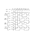
図4にはDFF回路301をセットおよびDFF回路302をリセットすることによる分周精度の微調整について説明するタイミングチャートを示す。
【0046】
図中、CKタイミングチャート401はCK信号916のタイミングを示し、SRタイミングチャート402は、DFF回路301のセットおよびDFF回路302のリセット信号のタイミングを示す。
【0047】
SR無しタイミングチャート403は、セットが無い場合のQ1信号321とQ2信号322のタイミングを示し、セットタイミングチャート404はS信号317がSRタイミングチャート402にしたがってDFF回路301をセットした場合のQ1信号321とQ2信号322のタイミングを示す。
【0048】
リセットタイミングチャート405は、R信号318がSRタイミングチャート402にしたがってDFF回路302をリセットした場合のQ1信号321とQ2信号322のタイミングを示し、SRセットタイミングチャート406は、SRタイミングチャート402にしたがってS信号317がDFF回路301をセットし、R信号318がDFF回路302に発生した場合のQ1信号321とQ2信号322のタイミングを示す。
【0049】
SR無しタイミングチャート403の場合、SRタイミングチャート402で示されるセットのタイミングを基準にQ1信号321の最初の立ち下がりはCK信号916の4番目の立ち下がりに同期して立ち下がる。
【0050】
セットタイミングチャート404の場合、SRタイミングチャート402で示されるセットのタイミングを基準にQ1信号321の最初の立ち下がりはCK信号916の1番目の立ち下がりに同期して立ち下がる。
【0051】
リセットタイミングチャート405の場合、SRタイミングチャート402で示されるリセットのタイミングを基準にQ1信号321の最初の立ち下がりは、CK信号916の3番目の立ち下がりに同期して立ち下がる。
【0052】
セットリセットタイミングチャート406の場合、SRタイミングチャート402で示されるセットリセットのタイミングを基準にQ1信号321の最初の立ち下がりはCK信号916の2番目の立ち下がりに同期して立ち下がる。
【0053】
すなわち、S信号317およびR信号318を入力してQ1信号321のタイミングを変化させることによって最終的に発生されるQ15信号335の周期を微調整できる。
【0054】
また、今までの回路と置き換える場合はセットおよびリセット入力をデコードすることなどによってつなぎかえることによって、簡単に置き換えることが可能である。
【0055】
(第2の実施形態:図5および図6)
つぎに第2の実施形態における分周回路の構成を図5を用いて説明する。第1の実施の形態で示した微調整機能付き低電力分周回路が立ち上がり同期の場合の回路を説明する。
【0056】
図5は本発明の微調整機能付きの低電力の分周回路を示しており、第1番目のDFF回路501から第15番目のDFF回路515から構成されている。
【0057】
図5において、DFF回路501はR信号517を入力するためのリセット付きのDFF回路であり、水晶発振器から発生されたクロックパルスであるCK信号916の立ち上がりに同期して1/4分周されたQ1信号521を出力する回路である。
【0058】
DFF回路502はS信号518を入力するためのセット付きのDFF回路であり、CK信号916の立ち上がりに同期して1/4分周されたQ2信号522を出力する回路である。
【0059】
DFF回路503はDFF回路501から発生されたQ1信号521の立ち上がりに同期して1/2分周されたQ3信号523を出力する回路であり、DFF回路504はDFF回路503から発生されたQ3信号523の立ち上がりに同期して1/2分周されたQ4信号524を出力する回路である。
【0060】
以下、同じようにしてDFF回路515は約1HzのQ15信号535を出力する。
【0061】
図6にはDFF回路501をリセットおよびDFF回路502をセットすることによる分周精度の微調整について説明するタイミングチャートを示す。
【0062】
図6において、CKタイミングチャート601はCK信号916のタイミングを示し、RSタイミングチャート602はDFF回路501のリセットとDFF回路502のセット信号のタイミングを示す。
【0063】
RS無しタイミングチャート603は、セットが無い場合のQ1信号521とQ2信号522のタイミングを示し、リセットタイミングチャート604はR信号517がSRタイミングチャート602にしたがってDFF回路901をリセットした場合のQ1信号521とQ2信号522のタイミングを示す。
【0064】
セットタイミングチャート605は、S信号518がSRタイミングチャート602にしたがってDFF回路502をセットした場合のQ1信号521とQ2信号522のタイミングを示し、RSセットタイミングチャート606はR信号517が、SRタイミングチャート602にしたがってDFF回路501をリセットし、S信号518がSRタイミングチャート602にしたがってDFF回路502をセットした場合のQ1信号521およびQ2信号522のタイミングを示す。
【0065】
RS無しタイミングチャート603の場合、RSタイミングチャート602で示されるセットのタイミングを基準にQ1信号521の最初の立ち上がりはCK信号916の4番目の立ち上がりに同期して立ち上がる。
【0066】
セットタイミングチャート604の場合、RSタイミングチャート602で示されるセットのタイミングを基準にQ1信号521の最初の立ち上がりはCK信号916の1番目の立ち上がりに同期して立ち上がる。
【0067】
リセットタイミングチャート605の場合、RSタイミングチャート602にて示されるリセットのタイミングを基準にQ1信号521の最初の立ち上がりはCK信号916の3番目の立ち上がりに同期して立ち上がる。
【0068】
リセットセットタイミングチャート606の場合、RSタイミングチャート602で示されるリセットセットのタイミングを基準にQ1信号521の最初の立ち上がりはCK信号916の2番目の立ち上がりに同期して立ち上がる。
【0069】
すなわち、R信号517およびS信号518を入力してQ1信号521のタイミングを変化させることによって最終的に発生されるQ15信号535の周期を微調整できる。
【0070】
また、今までの回路と置き換える場合はセットおよびリセット入力をデコードすることなどによってつなぎかえることにより、簡単に置き換えることが可能である。
【0071】
(第3の実施形態:図7および図8)
つぎに第3の実施形態における分周回路の構成を図7を用いて説明する。第1の実施形態で示した微調整機能付き低電力の分周回路のジョンソンカウンタ部分のDFF回路段数が4段の場合の回路を説明する。
【0072】
図7は本発明の微調整機能付きの低電力の分周回路を示しており、第1番目のDFF回路701から第17番目のDFF回路717から構成されている。
【0073】
図7において、DFF回路701はS信号730を入力するためのセット付きのDFF回路であり、水晶発振器から発生されたクロックパルスであるCK信号916の立ち下がりに同期して1/8分周されたQ1信号721を出力する回路である。
【0074】
DFF回路702はR1信号731を入力するためのリセット付きのDFF回路であり、CK信号916の立ち下がりに同期して1/8分周されたQ1信号721を出力する回路である。
【0075】
以下同様に、DFF回路703はR2信号732を入力するためのリセット付きのDFF回路であり、CK信号916の立ち下がりに同期して1/8分周されたQ3信号723を出力する回路であり、DFF回路704はR3信号733を入力するためのリセット付きのDFF回路であり、CK信号916の立ち下がりに同期して1/8分周されたQ4信号724を出力する回路である。
【0076】
DFF回路705はDFF回路701から発生されたQ1信号721の立ち下がりに同期して1/2分周されたQ5信号725を出力する回路であり、DFF回路706はDFF回路705から発生されたQ5信号725の立ち下がりに同期して1/2分周されたQ6信号726を出力する回路である。
【0077】
以下、同じようにしてDFF回路717は約1HzのQ17信号737を出力する。
【0078】
図8にはDFF回路701をセットとDFF回路702、DFF回路703とDFF回路704をリセットすることによる分周精度の微調整について説明するタイミングチャートを示す。
【0079】
図8において、CKタイミングチャート801はCK信号916のタイミングを示し、SRタイミングチャート802はDFF回路701のセットとDFF回路702、DFF回路703およびDFF回路704のリセット信号のタイミングを示す。
【0080】
SR無しタイミングチャート803はセットが無い場合のQ1信号721、Q2信号722、Q3信号723およびQ4信号724のタイミングを示す。
R1R2タイミングチャート804はSRタイミングチャート802にしたがってR1信号731がDFF回路702をリセットし、R2信号732がDFF回路703をリセット場合のQ1信号721、Q2信号722、Q3信号723およびQ4信号724のタイミングを示す。
【0081】
SR無しタイミングチャート803の場合、SRタイミングチャート802で示されるセットのタイミングを基準にQ1信号821の最初の立ち下がりはCK信号916の8番目の立ち下がりに同期して立ち下がる。
【0082】
R1R2リセットタイミングチャート804の場合、SRタイミングチャート802で示されるセットのタイミングを基準にQ1信号721の最初の立ち下がりはCK信号916の6番目の立ち下がりに同期して立ち下がる。
【0083】
以下、1つのセットと3つのリセットを組み合わせることによってSRタイミングチャート802で示されるセットのタイミングを基準にQ1信号721の最初の立ち下がりをCK信号916の1番目から8番目の立ち下がりに同期して立ち下げることが可能である。
【0084】
すなわち、S信号730、R1信号731、R2信号732、およびR3信号733を入力してQ1信号721のタイミングを変化させることによって最終的に発生されるQ15信号735の周期を微調整できる。
【0085】
もちろん、ジョンソンカウンタ部分のリセット付きDFF回路を増やしても微調整が可能である。
また、今までの回路と置き換える場合はセットおよびリセット入力をデコードすることなどによってつなぎかえることにより、簡単に置き換えることが可能である。
【0086】
【発明の効果】
以上の説明からあきらかなように、本発明の分周回路によって電子時計などの分周回路を用いる電子機器を、精度を維持しながら低電力で分周することが可能となる。
【図面の簡単な説明】
【図1】 参考例として分周回路の発振回路を含んだ構成を示す回路図である。
【図2】 図1の例における分周回路の電流測定結果を示すグラフである。
【図3】 本発明の実施の形態における微調整機能付き分周回路の構成を示す回路図である。
【図4】 本発明の実施形態における分周回路によるタイミングチャートを示す図面である。
【図5】 本発明の実施形態における分周回路による立ち上がり同期時を示す回路図である。
【図6】 本発明の実施形態における分周回路によるタイミングチャートを示す図面である。
【図7】 本発明の実施形態における分周回路による立ち上がり同期時を示す回路図である。
【図8】 本発明の実施形態における分周回路による1/8分周を基にしたタイミングチャートを示す図面である。
【図9】 従来技術における分周回路を示す回路図である。
【図10】 従来技術における分周回路によるタイミングチャートを示す図面である。
【符号の説明】
110:ジョンソンカウンタ部
111:バイナリカウンタ部
116:CK信号
131:容量Cout
201:本発明による回路の電流−周波数特性
203:本発明による回路の電流−電圧特性
321:Q1信号
404:セットタイミングチャート
604:リセットタイミングチャート
804:R2R3タイミングチャート[0001]
BACKGROUND OF THE INVENTION
The present invention relates to a configuration of a frequency dividing circuit used in an electronic timepiece or the like, and more particularly to a frequency dividing circuit of low power and frequency dividing accuracy technology.
[0002]
[Prior art]
Frequency divider circuits are used in various electronic devices. Particularly in electronic watches, the frequency divider plays a central role.
[0003]
The current electronic timepiece divides the frequency until 1 second based on a clock pulse generated from a crystal oscillator circuit of about 32 KHz and displays the time in seconds.
Frequency division is performed by a frequency dividing circuit, and the frequency dividing circuit can perform fine adjustment to absorb frequency deviation due to manufacturing variations in addition to frequency division.
[0004]
The circuit diagram of FIG. 9 shows a conventional binary counter type frequency divider circuit, which is composed of a first data type flip-flop circuit (DFF circuit) 901 to a
[0005]
In FIG. 9, the
[0006]
The
[0007]
The
[0008]
Thereafter, the frequency is similarly divided, and the
[0009]
FIG. 10 is a waveform diagram showing a timing chart for explaining fine adjustment of the frequency division accuracy by setting the
[0010]
In FIG. 10, a
[0011]
The no-set
[0012]
The S2 set
[0013]
In the case of the no-set
[0014]
Further, in the case of the S1 set
[0015]
In the case of the S2 set
[0016]
In the case of the S1-2 set
[0017]
That is, by inputting S1 and S2 and changing the timing of the
[0018]
[Problems to be solved by the invention]
In the frequency divider circuit of the electronic timepiece as shown in FIG. 9 using only the binary counter type frequency divider circuit, there are many gates driven at a high frequency, and thus there is a limit to the reduction in power consumption.
[0019]
(Object of invention)
In order to solve the above problems, an object of the present invention is to devise the form of a frequency dividing circuit, and to propose a frequency dividing circuit including a frequency dividing circuit that can finely adjust the frequency division with low power.
[0020]
[Means for Solving the Problems]
In order to achieve the above object, the present invention is a frequency dividing circuit for inputting a clock signal having a predetermined frequency generated from an oscillation circuit , dividing the clock signal, and outputting a signal having a predetermined frequency dividing ratio.
A synchronous front-end circuit that includes a plurality of flip-flop circuits having either a set function or a reset function and that divides the frequency based on the clock signal ;
Have a, and the rear portion circuit asynchronous for dividing based on the divided signal outputted as a result of the front stage circuit with the flip-flop circuit comprising a plurality of stages,
In a frequency divider circuit that enables fine adjustment of the predetermined frequency division ratio by enabling the set function or the reset function by inputting a predetermined adjustment signal,
The pre-stage circuit is connected so as to transfer the capacitance of the clock input gate to the capacitance Cout constituting the oscillation circuit by directly inputting the clock signal as a clock input,
The pre-stage circuit divides the clock signal up to at least 1/4 frequency division based on the clock signal,
The first part circuit, when provided with the set function and a flip-flop circuit at least Kumisonae, to the first stage of the flip-flop circuit having a flip-flop circuit and reset function having a set function, other of the flip-flop circuit with the reset function, when provided with the reset function to the first stage of the flip-flop circuit, another one of the flip-flop circuit comprises a set of functions,
The adjustment signal is two signals of a set signal for enabling the set function and a reset signal for enabling the reset function,
The pre-stage circuit changes the start timing of the output signal of the first flip-flop circuit in synchronization with the fall or rise of the clock signal by the combination of the two signals that are the adjustment signals .
[0021]
[Action]
Usually, the preceding stage of the frequency dividing circuit in the timepiece circuit is an oscillation circuit as shown in FIG. Therefore, the clock input of the frequency divider circuit is the power consumption of the inverter circuit in the oscillation circuit 130.
[0022]
By the way, Cout 131 is originally required for transmission, and even if a part of the capacity of the clock input gate of the frequency divider circuit is transferred to Cout, the power consumption of the oscillation circuit 130 does not change.
[0023]
Therefore, the power can be reduced by using a synchronous counter type frequency dividing circuit such as a Johnson counter that can lower the gate driving frequency other than the clock gate driven by the CK signal 116 from the oscillation circuit 130 of the frequency dividing circuit.
[0024]
The above effect is more effective at high frequencies. However, the Johnson counter type circuit requires a larger circuit area than the binary counter type frequency dividing circuit in the same frequency dividing function, and further, there is a limit to supplement a part of
[0025]
Further, the fine adjustment function, which is another role of the frequency dividing circuit, can be easily realized by using a DFF circuit with a set and a reset in the Johnson counter unit.
[0026]
DETAILED DESCRIPTION OF THE INVENTION
(Reference Example: FIGS. 1 and 2)
Hereinafter, the configuration of the frequency dividing circuit which is a premise of the present invention will be described with reference to the drawings. FIG. 1 is a diagram showing the configuration of the frequency dividing circuit. The frequency dividing circuit is formed of two parts, a Johnson counter unit 110 and a binary counter unit 111.
[0027]
The Johnson counter portion 110 is a Johnson counter circuit composed of two well-known DFF circuits, a
[0028]
The binary counter portion 111 is a binary counter circuit composed of four DFF circuits, which are generally well-known
[0029]
The
[0030]
The
[0031]
FIG. 2 shows a current measurement result of the above-described frequency dividing circuit according to the present invention for performing 1/64 frequency division manufactured by a predetermined C-MOS process and a binary counter type frequency dividing circuit (not shown) in the prior art. Indicates.
In FIG. 2, the points indicated by squares indicate the current measurement results of the binary counter type frequency divider circuit in the prior art, and the points indicated by circles indicate the current measurement results of the frequency divider circuit according to the present invention.
[0032]
FIG. 2A shows the frequency dependence at a constant voltage (0.7 V). The characteristics of any of the frequency dividing circuits are substantially proportional to the frequency, but the
[0033]
FIG. 2B shows the voltage dependence at a constant frequency (32 KHz). Although the characteristics of any of the frequency divider circuits are substantially proportional to the voltage, the
[0034]
In the conventional binary counter type frequency divider circuit, the Q1 signal divided by 1/2 is input to the second stage DFF circuit, whereas in the Johnson counter unit 110, the Q1 signal 121 and the Q2 signal 122 are This is because the signal is divided by 1/4 and driven at a relatively low frequency.
[0035]
The driving power by the
[0036]
In this way, a low-power frequency divider circuit can be manufactured. Of course, it is possible to further reduce the power by increasing the number of stages of the Johnson counter system 110. However, the gate capacity that is larger than the optimum value of the capacity Cout131 is in terms of total power and stability. It is not preferable.
[0037]
Further, the binary counter type frequency dividing circuit has a frequency dividing function of 1 /
For this reason, it is desirable to make the circuit well balanced with the binary counter type frequency dividing circuit. In particular, when the Johnson type counter unit 110 is composed of two stages of DFF circuits, the number of DFF circuits is the same as the number of binary counter type frequency divider circuits.
[0038]
In this example, the Johnson counter type circuit has been described, but the same effect can be obtained with a synchronous circuit.
[0039]
(First Embodiment: FIGS. 3 and 4)
Next, the configuration of the frequency divider in the first embodiment will be described with reference to FIG. A circuit in which a fine adjustment function is added to the low power divider circuit shown in the reference example will be described.
[0040]
FIG. 3 shows a low-power frequency divider circuit with a fine adjustment function according to the present invention, which includes a
[0041]
In FIG. 3, a
[0042]
The
[0043]
The
[0044]
Thereafter, the
[0045]
FIG. 4 is a timing chart for explaining fine adjustment of the frequency division accuracy by setting the
[0046]
In the figure, a
[0047]
The
[0048]
The
[0049]
In the case of the
[0050]
In the case of the
[0051]
In the case of the
[0052]
In the case of the set reset
[0053]
That is, the period of the Q15 signal 335 finally generated can be finely adjusted by inputting the S signal 317 and the
[0054]
In addition, when replacing the circuit so far, it is possible to easily replace it by changing the input by decoding the set and reset inputs.
[0055]
(Second Embodiment: FIGS. 5 and 6)
Next, the configuration of the frequency divider in the second embodiment will be described with reference to FIG. A circuit in the case where the low power divider circuit with a fine adjustment function shown in the first embodiment is in synchronization with rising is described.
[0056]
FIG. 5 shows a low-power frequency divider circuit with a fine adjustment function according to the present invention, which includes a
[0057]
In FIG. 5, a
[0058]
The
[0059]
The
[0060]
Thereafter, the
[0061]
FIG. 6 is a timing chart for explaining fine adjustment of the frequency division accuracy by resetting the
[0062]
In FIG. 6, a
[0063]
The
[0064]
The
[0065]
In the case of the
[0066]
In the case of the
[0067]
In the case of the
[0068]
In the case of the reset set
[0069]
That is, the period of the Q15 signal 535 that is finally generated can be finely adjusted by inputting the
[0070]
In addition, when replacing the circuit so far, it is possible to easily replace it by changing the input by decoding the set and reset inputs.
[0071]
( Third embodiment: FIGS. 7 and 8)
Then the frequency divider of the structure in the third embodiment will be described with reference to FIG. DFF circuit number of Johnson counter part of the fine adjustment function Low power divider circuit shown in the first exemplary type state is illustrating a circuit in the case of 4 stages.
[0072]
FIG. 7 shows a low-power frequency divider circuit with a fine adjustment function according to the present invention, which is composed of a
[0073]
In FIG. 7, a
[0074]
The
[0075]
Similarly, the
[0076]
The
[0077]
Thereafter, the
[0078]
FIG. 8 is a timing chart for explaining fine adjustment of frequency division accuracy by setting the
[0079]
In FIG. 8, a
[0080]
The SR-free timing chart 803 shows the timing of the
The
[0081]
In the case of the timing chart 803 without SR, the first falling edge of the Q1 signal 821 falls in synchronization with the eighth falling edge of the CK signal 916 with reference to the timing of the set shown in the
[0082]
In the case of the R1R2
[0083]
Hereinafter, by combining one set and three resets, the first falling edge of the
[0084]
That is, the period of the Q15 signal 735 finally generated can be finely adjusted by inputting the S signal 730, the
[0085]
Of course, fine adjustment is possible even if the number of DFF circuits with reset in the Johnson counter portion is increased.
In addition, when replacing the circuit so far, it is possible to easily replace it by changing the input by decoding the set and reset inputs.
[0086]
【The invention's effect】
As is clear from the above description, it is possible to divide an electronic device using a frequency dividing circuit such as an electronic timepiece with low power while maintaining accuracy by the frequency dividing circuit of the present invention.
[Brief description of the drawings]
FIG. 1 is a circuit diagram showing a configuration including an oscillation circuit of a frequency divider as a reference example .
FIG. 2 is a graph showing a current measurement result of a frequency divider circuit in the example of FIG.
FIG. 3 is a circuit diagram showing a configuration of a frequency dividing circuit with a fine adjustment function in the embodiment of the present invention.
FIG. 4 is a diagram showing a timing chart by the frequency divider circuit in the embodiment of the present invention.
FIG. 5 is a circuit diagram showing a rising synchronization time by a frequency divider in an embodiment of the present invention.
FIG. 6 is a diagram showing a timing chart by the frequency divider circuit in the embodiment of the present invention.
FIG. 7 is a circuit diagram showing a rising synchronization time by a frequency divider in the embodiment of the present invention.
FIG. 8 is a drawing showing a timing chart based on 1/8 frequency division by a frequency divider circuit in an embodiment of the present invention.
FIG. 9 is a circuit diagram showing a frequency dividing circuit in the prior art.
FIG. 10 is a diagram showing a timing chart by a frequency dividing circuit in the prior art.
[Explanation of symbols]
110: Johnson counter unit 111: Binary counter unit 116: CK signal 131: Capacitance Cout
201: Current-frequency characteristics of a circuit according to the present invention 203: Current-voltage characteristics of a circuit according to the present invention 321: Q1 signal 404: Set timing chart 604: Reset timing chart 804: R2R3 timing chart
Claims (1)
セット機能またはリセット機能のどちらかを有するフリップフロップ回路を複数段備えると共に前記クロック信号を基に分周する同期式の前段部回路と、
フリップフロップ回路を複数段備えると共に前記前段部回路の結果として出力される分周信号を基に分周する非同期式の後段部回路と、を有し、
所定の調整信号を入力することで、前記セット機能または前記リセット機能を有効にして前記所定の分周比の微調整ができる分周回路において、
前記前段部回路は、前記クロック信号をクロック入力として直接入力することで、クロック入力ゲートの容量を前記発振回路を構成する容量Coutに繰り込むように接続され、
前記前段部回路は、前記クロック信号の少なくとも1/4分周までを前記クロック信号を基に分周し、
前記前段部回路は、セット機能を有するフリップフロップ回路とリセット機能を有するフリップフロップ回路とを少なくとも1組備え、初段の前記フリップフロップ回路に前記セット機能を備えたとき、他の前記フリップフロップ回路は前記リセット機能を備え、初段の前記フリップフロップ回路に前記リセット機能を備えたとき、他の前記フリップフロップ回路は前記セット機能を備え、
前記調整信号は、前記セット機能を有効にするセット信号と、前記リセット機能を有効にするリセット信号と、の2つの信号であり、
前記前段部回路は、前記調整信号である前記2つの信号の組み合わせにより、前記クロック信号の立ち下がりまたは立ち上がりに同期して初段の前記フリップフロップ回路の出力信号の開始タイミングを変化させることを特徴とする分周回路。 A frequency dividing circuit for inputting a clock signal having a predetermined frequency generated from an oscillation circuit, dividing the clock signal and outputting a signal having a predetermined frequency dividing ratio,
A synchronous front-end circuit that includes a plurality of flip-flop circuits having either a set function or a reset function and that divides the frequency based on the clock signal ;
Have a, and the rear portion circuit asynchronous for dividing based on the divided signal outputted as a result of the front stage circuit with the flip-flop circuit comprising a plurality of stages,
In a frequency divider circuit that enables fine adjustment of the predetermined frequency division ratio by enabling the set function or the reset function by inputting a predetermined adjustment signal,
The pre-stage circuit is connected so as to transfer the capacitance of the clock input gate to the capacitance Cout constituting the oscillation circuit by directly inputting the clock signal as a clock input,
The pre-stage circuit divides the clock signal up to at least 1/4 frequency division based on the clock signal,
The first part circuit, when provided with the set function and a flip-flop circuit at least Kumisonae, to the first stage of the flip-flop circuit having a flip-flop circuit and reset function having a set function, other of the flip-flop circuit with the reset function, when provided with the reset function to the first stage of the flip-flop circuit, another one of the flip-flop circuit comprises a set of functions,
The adjustment signal is two signals of a set signal for enabling the set function and a reset signal for enabling the reset function,
The pre-stage circuit changes the start timing of the output signal of the flip-flop circuit in the first stage in synchronization with the fall or rise of the clock signal by a combination of the two signals as the adjustment signal. Dividing circuit to do.
Priority Applications (1)
| Application Number | Priority Date | Filing Date | Title |
|---|---|---|---|
| JP2000112792A JP4149634B2 (en) | 2000-04-14 | 2000-04-14 | Frequency divider circuit |
Applications Claiming Priority (1)
| Application Number | Priority Date | Filing Date | Title |
|---|---|---|---|
| JP2000112792A JP4149634B2 (en) | 2000-04-14 | 2000-04-14 | Frequency divider circuit |
Publications (3)
| Publication Number | Publication Date |
|---|---|
| JP2001298358A JP2001298358A (en) | 2001-10-26 |
| JP2001298358A5 JP2001298358A5 (en) | 2007-04-05 |
| JP4149634B2 true JP4149634B2 (en) | 2008-09-10 |
Family
ID=18624888
Family Applications (1)
| Application Number | Title | Priority Date | Filing Date |
|---|---|---|---|
| JP2000112792A Expired - Fee Related JP4149634B2 (en) | 2000-04-14 | 2000-04-14 | Frequency divider circuit |
Country Status (1)
| Country | Link |
|---|---|
| JP (1) | JP4149634B2 (en) |
Families Citing this family (1)
| Publication number | Priority date | Publication date | Assignee | Title |
|---|---|---|---|---|
| US8355478B1 (en) * | 2009-05-29 | 2013-01-15 | Honeywell International Inc. | Circuit for aligning clock to parallel data |
-
2000
- 2000-04-14 JP JP2000112792A patent/JP4149634B2/en not_active Expired - Fee Related
Also Published As
| Publication number | Publication date |
|---|---|
| JP2001298358A (en) | 2001-10-26 |
Similar Documents
| Publication | Publication Date | Title |
|---|---|---|
| JPS6161283B2 (en) | ||
| GB1570659A (en) | Electronic timepiece | |
| US5606293A (en) | Clock generator for microcomputer having reduced start-up time | |
| JP4149634B2 (en) | Frequency divider circuit | |
| JP3523362B2 (en) | Clock circuit and processor using the same | |
| JP2002305443A (en) | Timer circuit | |
| US7387433B2 (en) | Integrated circuit chip for analogue electronic watch applications | |
| JPS60804B2 (en) | electronic clock | |
| JP3171963B2 (en) | Semiconductor integrated circuit | |
| US20020063591A1 (en) | Divider with cycle time correction | |
| JPH0983356A (en) | Clock generating circuit | |
| JP2622853B2 (en) | Doubler circuit | |
| JPH067383Y2 (en) | Clock generator | |
| JPH09214307A (en) | Clock circuit | |
| JP2002181971A (en) | Real-time clock | |
| JP3332940B2 (en) | Voltage controlled oscillator | |
| JP2002202828A (en) | Clock generating circuit | |
| JPH0719012Y2 (en) | Voltage detection circuit | |
| KR0167226B1 (en) | Odd/even detecting circuit | |
| JP2718191B2 (en) | Microcomputer standby circuit | |
| JPH0411194Y2 (en) | ||
| JP2636313B2 (en) | Clock generation circuit | |
| JPH03758Y2 (en) | ||
| KR940012090A (en) | Clock divider | |
| JPS6227911Y2 (en) |
Legal Events
| Date | Code | Title | Description |
|---|---|---|---|
| A521 | Written amendment |
Free format text: JAPANESE INTERMEDIATE CODE: A523 Effective date: 20070215 |
|
| A621 | Written request for application examination |
Free format text: JAPANESE INTERMEDIATE CODE: A621 Effective date: 20070215 |
|
| A977 | Report on retrieval |
Free format text: JAPANESE INTERMEDIATE CODE: A971007 Effective date: 20071225 |
|
| A131 | Notification of reasons for refusal |
Free format text: JAPANESE INTERMEDIATE CODE: A131 Effective date: 20080311 |
|
| A521 | Written amendment |
Free format text: JAPANESE INTERMEDIATE CODE: A523 Effective date: 20080509 |
|
| RD03 | Notification of appointment of power of attorney |
Free format text: JAPANESE INTERMEDIATE CODE: A7423 Effective date: 20080509 |
|
| TRDD | Decision of grant or rejection written | ||
| A01 | Written decision to grant a patent or to grant a registration (utility model) |
Free format text: JAPANESE INTERMEDIATE CODE: A01 Effective date: 20080624 |
|
| A01 | Written decision to grant a patent or to grant a registration (utility model) |
Free format text: JAPANESE INTERMEDIATE CODE: A01 |
|
| A61 | First payment of annual fees (during grant procedure) |
Free format text: JAPANESE INTERMEDIATE CODE: A61 Effective date: 20080626 |
|
| FPAY | Renewal fee payment (event date is renewal date of database) |
Free format text: PAYMENT UNTIL: 20110704 Year of fee payment: 3 |
|
| R150 | Certificate of patent or registration of utility model |
Free format text: JAPANESE INTERMEDIATE CODE: R150 |
|
| LAPS | Cancellation because of no payment of annual fees |