JP4138421B2 - Droplet discharge head - Google Patents
Droplet discharge head Download PDFInfo
- Publication number
- JP4138421B2 JP4138421B2 JP2002276473A JP2002276473A JP4138421B2 JP 4138421 B2 JP4138421 B2 JP 4138421B2 JP 2002276473 A JP2002276473 A JP 2002276473A JP 2002276473 A JP2002276473 A JP 2002276473A JP 4138421 B2 JP4138421 B2 JP 4138421B2
- Authority
- JP
- Japan
- Prior art keywords
- electret
- inorganic
- electrode
- polarization
- actuator
- Prior art date
- Legal status (The legal status is an assumption and is not a legal conclusion. Google has not performed a legal analysis and makes no representation as to the accuracy of the status listed.)
- Expired - Fee Related
Links
Images


Landscapes
- Particle Formation And Scattering Control In Inkjet Printers (AREA)
- Coating Apparatus (AREA)
- Physical Vapour Deposition (AREA)
- Chemical Vapour Deposition (AREA)
Description
【0001】
【産業上の利用分野】
本発明は無機エレクトレットアクチュエータを用いた液滴吐出ヘッドに関する。
【0002】
【従来の技術】
インクジェットヘッドなどの液滴吐出ヘッド、マイクロポンプ、マイクロ光変調デバイス、光スイッチなどの光学デバイス、マイクロスイッチ(マイクロリレー)、マイクロ流量計、圧力センサ、マイクロモータなどの各種マイクロデバイスにおいては、マイクロアクチュエータが用いられる。
【0003】
例えば、プリンタ、ファクシミリ、複写装置、プロッタ等の画像記録装置(画像形成装置)として用いるインクジェット記録装置に使用するインクジェットヘッドでは、インク流路内のインクを加圧するエネルギーを発生するアクチュエータ手段として振動板を変形させる圧電素子などの圧電型アクチュエータや静電型アクチュエータが用いられる。
【0004】
【発明が解決しようとする課題】
ところで、機械的駆動を行うことができるアクチュエータとしては、上述したようなPZTを主体とする圧電型アクチュエータや静電力を用いる静電型アクチュエータがあるが、前者の圧電型アクチュエータは鉛を含むPZTが主体であり、また後者の静電型アクチュエータは発生できる駆動力がさほど大きくないという課題がある。
【0005】
本発明は上記の課題に鑑みてなされたものであり、無機エレクトレットアクチュエータを用いた相互干渉の低減した微細分割駆動が可能な液滴吐出ヘッドを提供することを目的とする。
【0006】
【課題を解決するための手段】
上記の課題を解決するため、本発明に係る液滴吐出ヘッドは、
液滴を吐出させる液滴吐出ヘッドにおいて、
前記液滴を吐出させる圧力を発生させるアクチュエータとして、前記液滴吐出ヘッドの振動板上に無機材料を配向分極、イオン分極、電子分極させたエレクトレット層及び電極を形成して無鉛の無機エレクトレットアクチュエータを構成し、
前記振動板の剛性が5000〜12000kg/mm 2 の範囲であって、かつ、前記振動板の膜厚が前記エレクトレット層及び電極の厚み以下で、前記電極の幅に対して前記エレクトレット層の層厚が1/5以下である
構成とした。
【0007】
本発明に係る液滴吐出ヘッドは、
液滴を吐出させる液滴吐出ヘッドにおいて、
前記液滴を吐出させる圧力を発生させるアクチュエータとして、前記液滴吐出ヘッドの振動板上に無機材料を配向分極、イオン分極、電子分極させたエレクトレット層及び電極を形成して無鉛の無機エレクトレットアクチュエータを構成し、
前記振動板の剛性が5000〜12000kg/mm 2 の範囲であって、かつ、前記振動板の膜厚が前記エレクトレット層及び電極の厚み以下で、前記エレクトレット層を不完全分割して複数のアクチュエータ部に分割する溝が形成され、前記溝部に対応する前記エレクトレット層の厚さが前記エレクトレット層の厚さの1/2以下である
構成とした。
【0038】
【発明の実施の形態】
以下、本発明の実施の形態を添付図面を参照して説明する。
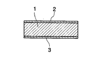
請求項1の発明に係る無機エレクトレットアクチュエータの実施形態について図1を参照して説明する。
無機エレクトレットアクチュエータは、無機材料を配向分極、イオン分極、電子分極させたエレクトレット層1を含み、このエレクトレット層1の両面に電極2、3を設けたものである。
【0039】
無機材料は陽イオン性、負イオン性の材料、または陽極性、負極性の分子団、或いは、電気陰性度の異なるイオン元素、または原子団を含ませて結晶化させて、電界を与え配向分極、イオン分極、電子分極させてエレクトレット層1を構成する。このエレクトレット層1の電極2,3間に矩形波、あるいは交番電圧を印加することで、全体としてモノモルフ振動或いはモノモルフ機械的駆動が生起する。
【0040】
このような無機エレクトレットアクチュエータの製造工程の一例のついて図2及び図3を参照して説明する。
先ず、図2に示すように、例えば、コーデライトの2MgO・2Al2O3・5SiO2複合酸化物の微粉末(平均粒径0.5〜3μm)に微粉末(平均粒径0.5〜3μm)のLa2O3を0.5〜1wt%混合した材料12を、ベルト13上に供給してプレスローラ14で加圧、層厚規制をしながら厚み50μmのグリーンシート11を形成し、このグリーンシート11上にカバーシート15を供給して加圧ローラ16で加圧することで、図3(a)に示すようなグリーンシート部材を得る。
【0041】
そして、図3(b)に示すようにグリーンシート11に脱水処理を施し、同図(b)に示すように400〜500℃で一次焼成を行い、更に同図(d)に示すように、850〜1200℃で焼成させると、高剛性(8000〜15000kg/mm2)の結晶歪みの大きな材料21が得られる。この材料21は結晶性と非晶体の混合組成である。
【0042】
その後、同図(e)に示すように材料11の両面に金属電極2、3を付け、同図(f)に示すように大気中で、450℃雰囲気に置き、電極2、3間にDC300Vを印加させ、1時間保持した後、同(g)に示すようにDC300V電界印加のまま除冷させ室温になるまで放置する。これにより、同図(h)に示すように、配向、分極が生じて、結晶体部分は大きく歪みを保持したまま維持され、内部分極が大きい状態で無機エレクトレット化したエレクトレット層1が得られる。
【0043】
ここで、この無機エレクトレットアクチュエータを用いたデバイスの基本構成は、例えば変形可能部材(以下、「振動板」ともいう。)を、導電材料、或いは絶縁材料の表面に電極材料をコーテイングしたもので形成して、この振動板を下電極3とし、この下電極3に上記無機材料のペーストやゾル・ゲルをスクリーン印刷、或いはメタルマスク印刷し、焼結条件で無機酸化物を形成する。そして、メタルマスク印刷時あるいは、乾式や湿式のエッチングで目的素子に分割した後又は前に、上電極を金属ペーストの印刷で形成、焼結する。この上下電極2、3に電圧印加と加熱を同時に行って、無機エレクトレット化する。
【0044】
このように、無機材料を配向分極、イオン分極、電子分極させたエレクトレット層を含むことを無機エレクトレットアクチュエータを構成することで、無鉛の機械的強度の大きな新規なアクチュエータを得ることができる。
【0045】
次に、請求項2の発明に係る無機エレクトレットアクチュエータの実施形態について説明する。
ここでは、無機材料は、強誘電体、誘電体、または固体電解質材料を含む、さらに、これらの粒子配向セラミックスを包含するものである。具体的な材料としては、ZrTiO4−SnO2TiO2、Fe2O3−NiO、Zn2TiO2、ZnNiTiO4、ZnFe2O4、K2OAl2O3−SiO2、CaOAl2O3、BaTiO3、Al2O3TiO2、MgOAl2O3等多くの分極性無機材料がある。
【0046】
また、遷移金属系の添加により、多価原子団によるイオン化、配向分極化が可能である。結晶構造としてはスピネル構造、ぺロブスカイト構造や焼結体の部分的に結晶化し、立方体、長方体、斜方体、菱面体等が存在する。
【0047】
焼結温度は材料の組み合わせと組成比や、原材料の出発材料、さらに材料の粒子依存性による。200℃〜1200℃程度であるが、通常は300℃〜600℃で良い結果が得られる。吸湿性や印加電圧による強電界による分極反転が起き機能劣化が発生するが、本例の雰囲気制御条件では、材料の脱水性、高酸化物状態であり、また表面電極金属膜保護により、信頼性、寿命は満足される。
【0048】
工程としては、これらの結晶の一部に歪みを形成させることが必要であるが、膜厚1μm〜300μm1μmで、300℃〜400℃の加熱温度で、印加電圧はDC50V〜500Vで十分である。
【0049】
また、粒子配向セラミックスとは焼結させたイオン性の異方性微粉末を一次焼結させ、さらに高温の加圧方向性を持たせ、二次加圧焼結結晶化させると、配向性セラミックスが得られ分極した状態になる。
【0050】
ここでも、この無機エレクトレットアクチュエータを用いたデバイスの基本構成は、例えば振動板を導電材料、或いは絶縁材料の表面に電極材料をコーテイングたもので形成して、これを下電極とし、この下電極に上記無機材料のペーストやゾル・ゲルをスクリーン印刷、或いはメタルマスク印刷し、焼結条件で無機酸化物を形成する。そして、メタルマスク印刷時あるいは、乾式や湿式のエッチングで目的素子に分割した後、次に、上電極を金属ペーストの印刷で形成、焼結する。この上下電極に電圧印加と加熱を同時に行って、無機エレクトレット化する。
【0051】
このように、無機材料が強誘電体、誘電体、又は固体電解質材料を含むことで、これらの材料は材料自体がダイポールモーメントを持ち分極配向性があるので、大きな変位量が得られる。
【0052】
次に、請求項3の発明に係る無機エレクトレットアクチュエータの実施形態について説明する。
ここでは、無機材料に目的金属イオンをイオン打ち込み装置で選択的に打ち込み組成化している。
【0053】
一般的には、有機材料では、コロナ放電によるものが多い。有機樹脂材料についてはフッソ樹脂系を始めナイロン(登録商標)11等、雑多のブレンド樹脂の表面に、電子打ち込みやイオン打ち込みにより結晶構造に欠陥発生を誘起させ、歪みを形成してイオン分極や電荷分極を行っている。
【0054】
これに対して、無機材料ではシリコンウエハの表面熱酸化膜SiO2(結晶性酸化シリコン膜)に電子線を照射し、格子欠陥を発生させ、電荷トラップ層を形成して、エレクトレット層を作成することができる。しかしながら、無機材料では電子打ち込みによる結晶歪みは小さく、効果が殆ど無い。
【0055】
そこで、ここでは、減圧中で金属イオンを打ち込むようにしている。このようなエレクトレット層の製作工程について図4を参照して説明する。
先ず、同図(a)に示すような複合酸化物31に、同図(b)に示すようにB、Sb、P、Ti、Bi、W、Mnなどの加速イオンを打ち込むと、同図(c)に示すように複合酸化物31の表面から100〜3000Å程度までイオンが入るが、ここでは、金属は混在する状態でイオン化していない結晶歪みのみである。
【0056】
さらに、同図(d)に示すように、焼結拡散処理(加熱拡散処理)を行うことで、金属イオンは0.5〜10μmに達しイオン化する。これにより、結晶歪みとイオン効果の相効果が発揮できる。そして、同図(e)に示すように電極2,3を付してエレクトレット化を行ってエレクトレット層1を形成する。この場合、イオン分極と電荷分極、配向分極は大きいものが得られる。
【0057】
このように、無機材料に目的金属イオンが選択的に打ち込まれて組成化されている構成とすることで、結晶歪みの増大と導入多価イオンの組成化でイオン配向と分極が大きくなる。
【0058】
次に、請求項4の発明に係る無機エレクトレットアクチュエータの実施形態について説明する。
ここでは、無機材料は、金属酸化物(TiO2、NiO、Al2O3、Fe2O3、MnO2、Co2O3/CoO、Sn2O3/SnO、ZnO等)やアルカリ土類元素化合酸化物(BaO、K2O、CaO、MgO等)と強誘電体、誘電体、または固体電解質材料を含むZrTiO4−SnO2TiO2、Fe2O3−NiO、Zn2TiO2、さらにZnNiTiO4、ZnFe2O4、K2OAl2O3−SiO2、CaOAl2O3、BaTiO3、Al2O3TiO2、MgOAl2O3等などの分極性無機材料の混合組成としたものである。
【0059】
特に、アルカリ土類元素の化合物は、その元素イオン団が陽イオンとして、他の無機材料が負イオンとして働き、その結晶性も大きく、イオン配向性が高い材料である。複合酸化物焼成時の酸化還元雰囲気制御で、イオン性の大きな材料が得られる。
【0060】
この実施形態の概念を図5に示している。同図の例はイオン団の陰性度による分極の例であり、配向、分極が容易に起こる。実際は、Mg2Al2O4やK2SiO3、BaFe2O4等の複合塩の物質が高温と電界で分極する。
【0061】
このように、無機材料が金属酸化物又はアルカリ土類金属酸化物を含む構成とすることで、イオン、電荷分極を大きくすることができる。
【0062】
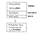
次に、請求項5の発明に係る無機エレクトレットアクチュエータの実施形態について説明する。
ZrTiO4−SnO2TiO2、Fe2O3−NiO、Zn2TiO2、さらにZnNiTiO4、ZnFe2O4、K2OAl2O3−SiO2、CaOAl2O3、BaTiO3、Al2O3TiO2、MgOAl2O3等などの分極性無機材料と、非金属元素のSiO2、B2O3、P2O5、Sb2O5、Bi2O3)の混合材料に、さらに遷移元素酸化物である(V2O5、Cr2O3、CuO、Y2O3、Zr2O3、Nb2O3、Mo2O3、PD2O3、La2O3等を混成させた複合酸化物は、この遷移元素を含む複合酸化物の焼成状態と雰囲気により、原子価制御が容易である。これは結晶歪みの大きさを結果として制御することができる。
【0063】
この実施形態の概念図を図6に示している。無機誘電体、多価非金属元素、遷移元素の混合酸化物は、焼成雰囲気、特に、多価原子と遷移元素は第2イオン化電位も低いことから、容易にイオン化し、加熱と電界でイオン分極、配向分極が生じる。
【0064】
このように、無機材料が遷移金属酸化物を含む複合酸化物である構成とすることで、多価元素の持つ、結晶体の中で未結合イオンが保持でき、大きなイオン分極が得られる。
【0065】
次に、請求項6の発明に係る無機エレクトレットアクチュエータの製造方法の実施形態について説明する。
無機材料の成膜は、次のような方法で行うことができる。
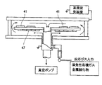
例えば、気相成長法を用いることができる。この場合には、プラズマCVD装置を用いて、例えば図7に示すように、無機材料の昇華性の高い有機金属、塩化物を減圧、加熱により下地電極を構成する基板41を保持したチャンバー内42に導入し、プラズマや酸化反応ガスと接触させ、気相成長させる。なお、同図中、43はノズル、44はアノード、45はカソード、46はモータ、47はヒータ、48は摺動接点である。また、平行平板電極型プラズマCVD装置の概略を図8に示している。
【0066】
また、蒸着法を用いることができる。この場合には、目的の無機材料や金属を加熱昇華させ、酸化性ガスをチャンバー内に導入し、蒸着法成膜で膜を形成する。
さらに、スパッタ法で金属材料はDC電源とスパッタガス(Ar,He,N2のどれかとさらにO2添加)による放電スパッタで行ない、導電性が無い無機材料は高周波電源を用いて同様のスパッタガスでRFスパッタを行なうことができる。
【0067】
CVD装置やスパッタ装置は、薄膜形成に適しており、その膜成長10〜300Å/分程度である。また、基板加熱により結晶成長させながら成膜することが容易にできる。
【0068】
これらのいずれかの方法を用いて成膜するとき、目的に合わせて、1層或いは多層成膜し、成膜時に基板加熱と反応ガスを導入し、プラズマ反応による酸化物や、チッ化物を形成させ、結晶性や非晶性を制御する。
【0069】
この場合、形成される薄膜は平坦であるので、次に上電極を蒸着法やホトリソ法で形成し、加熱と電界により、無機エレクトレット層とする。
【0070】
また、薄膜で分極効果が大きいことからアクチエータとして、マルチ化で各素子化するとき、上電極(前記電極2)の個別化のみで、素子分割せずとも各素子間の相互干渉は小さく、従来の分割工程は不要であり、微細分割が可能である。
【0071】
このように、無機材料を気相成長法又は蒸着法製膜で基板上に1層又は多層成膜し、成膜時に基板加熱と反応ガスを導入して、酸化物又はチッ化物を形成して結晶性又は非晶性を制御してエレクトレット層を形成することで、結晶性や非晶性を容易に制御することができる。
【0072】
次に、請求項7の発明に係る無機エレクトレットアクチュエータの製造方法の実施形態について説明する。
ここでは、無機材料は電着や蒸着で成膜し、これを陽極酸化させる。陽極酸化は、電極反応を伴いながら陰イオンと酸化する。そのため、酸化物形成と同時にイオンと電極反応するサイト部分がホール状態になり、酸化物がポーラス状態になる。例としては金属Alの陽極酸化生成物がよく知られている。
【0073】
酸化物は使用する無機酸(塩酸、硫酸、硝酸、過塩素酸)、無機酸と有機酸(蟻酸、酢酸、琥珀酸、蓚酸)、pH1〜6により酸化物膜中のポーラスサイズが50Å〜3μm程度の範囲で制御できる。また酸化物の膜厚は、陽極酸化反応の電解電流の電圧制御で規制できる。さらに、分極に必要な金属イオンを陽極酸化工程で添加し、このイオンを電気泳動で酸化物のポーラス孔に電着させ酸化物中に取り込むなど、必要に応じてポーラスの封孔を行ない、無機材料の平坦な薄膜を形成し、次に上電極を蒸着法やホトリソ法で形成し、加熱と電界により、無機エレクトレット層を作る。
【0074】
また、薄膜で分極効果が大きい事からアクチエータとして、マルチ化で各素子化する時、上電極の個別化のみで、素子分割せずとも各素子間の相互干渉は小さく、従来の分割工程は不要である。これを分極させると大きな分極配向材料が得られる。
【0075】
ここで、図9及び図10を参照してこの製造工程について説明する
図9(a)に示すように、開口55aを有する基板55上にNi−Cr、SUS等の金属材料からなる厚さ3〜100μm程度の下電極を兼ねた振動板(変形可能部材)53を設け、同図(b)に示すように、振動板53上に、蒸着法或いは電着法により、Al、Sn、Zn等の膜56を例えば3〜100μm厚に成膜する。
【0076】
そして、同図(c)に示すように、振動板53を+電位として、Pt等の負極となる対向電極を対向させて、酸浴中で電気化学反応を行うことで、図10に示すように孔57が発生し、孔57を通じて振動板53と対向電極とが電気的に通じ、酸浴中の陰イオンが移送され、化学反応を行い、陽極酸化膜58が形成される。
【0077】
その後、酸浴中に、遷移元素の金属イオンを導入して、孔57に電着させる。これを加熱処理(例えば300〜500℃)すると、複合酸化膜が得られる。そこで、同図(d)に示すように、個別電極となる上電極52を形成して、下電極である振動板53との間にDC100〜800Vの印加と300〜800℃の加熱を行うことで、複合酸化膜をエレクトレット化してエレクトレット層51を形成する。電極52と振動板53との間に電圧を印加することで、モノモルフ振動やモノモルフ機械駆動を行うことができる。
【0078】
このように、無機材料を電着又は蒸着で成膜し、陽極酸化させ、更に金属イオンを電気泳動で電着して、分極させて前記エレクトレット層を形成することで、薄膜プロセスとその結晶制御が容易になる。
【0079】
次に、請求項8の発明に係る無機エレクトレットアクチュエータの製造方法の実施形態について説明する。
無機材料は金属酸化物やアルカリ土類金属酸化物に、またはその混合材料に、遷移金属酸化物をボール・ミル混合器や乳鉢混合器でメカノケミカル混合する。これは、混合時に有機溶媒(アルコール、多価アルコール、や水、添加剤(PVA、デンプン)を加えて、攪拌粒子破砕するとゾルやゲル状態なる。これを脱気させ高粘張の塊を圧延ローラ等によりシート状(グリーンシート)に形成する。
【0080】
これを加熱するか、加熱と減圧脱気併用で複合酸化物とし、両面に電極焼き付けや、電極スクリーン印刷で形成し、これに加熱と電界処理を行ない、無機エレクトレット層を得る。
【0081】
ここで、図11及び図12を参照してこの製造工程について説明する。
まず、図11に示すように、上述したようにして得られるゾル・ゲル状態の無機材料72を、ベルト73上に供給してプレスローラ74で層厚規制をしながら所要厚のグリーンシート71を形成し、このグリーンシート11上にカバーシート75を供給してプレスローラ74、76で加圧して、次段の搬送ベルト77上に送り込み、カッター78で適当な長さに切断する。
【0082】
次いで、図12(a)に示すような上述したようにして得られたグリーンシート部材に、加熱、焼結を行って複合酸化物を形成し、同図(b)に示すように両面に電極62、63を形成して、これに加熱と電界処理を行ない、エレクトレット化を行ってエレクトレット層61を得る。
【0083】
このようにして得られた無機エレクトレットアクチュエータ60を例えば開口65aを形成した基板65に設けた振動板64上に接着剤67で接合する。電極62と振動板63との間に電圧を印加することで、モノモルフ振動やモノモルフ機械駆動を行うことができる。
【0084】
このように、無機材料をゾル又はゲル状態し、或いはシート状に成膜して、加熱又は加熱と減圧脱気を併用してエレクトレット層を形成することで、簡単な工程でエレクトレット層を形成できる。
【0085】
次に、請求項9の発明に係る無機エレクトレットアクチュエータの製造方法の実施形態について説明する。
無機材料層を形成して、低温で一次焼成と脱水処理を行う。この段階では、材料は化学付着水、化学結合水(水和物)を伴う酸化物である。例を上げるとSi-OH、Al-OH、Fe-OHなどが一部構成される不安定官能基が存在する。
【0086】
そこで、一次焼成体に、さらに適正加熱処理を行なうため、無機エレクトレット層を形成すると同時に適正加熱と電界を与えて、無機材料は、同一工程で、配向分極、イオン分極、電子分極を行なう。このとき、無機材料の化学組成は、雰囲気条件にもよるがSi-O-Si、若しくはSi=Oとなる。脱水がより完全になり、結晶化の原子団移動時に、電界の影響を原子団は大きく受け、イオン配向、電荷配向、分極配向の大きな材料が得られる。このエッレクトレット材料は大きな分極と科学的安定化による信頼性が向上する。
【0087】
ここで、図13を参照してこの製造工程の一例を説明する。
同図(a)に示すように、無機材料層を300〜600℃で低温焼成して一次焼成体85を得る。このとき、一次焼成体85はSi-OH、Al-OH、Fe-OH等の水酸基を持った状態にある。
【0088】
その後、同図(b)に示すように、電極82、83を形成して、800〜1200℃で焼成(加熱)を行うと同時に、DC200〜400Vの電圧を印加して、エレクトレット化を行ってエレクトレット層81を得る。このとき、加熱によって、Si-OHはK2SiO3など複合塩化合物になり、電界で配向、分極して固定される。
【0089】
このように、エレクトレット層を形成すると同時に加熱と電界を与えて、配向分極、イオン分極、電子分極を同時に行うことで、分極が容易になる。
【0090】
次に、請求項10の発明に係る無機エレクトレットアクチュエータの製造方法の実施形態について説明する。
無機材料層を形成し、適正高温加熱処理により、無機材料の化学組成は雰囲気条件にもよるがSi-O-Si、若しくはSi=Oとなる。脱水がより完全であり、化学量論組成に近い酸化物形成であり、結晶化が進んでいるもので、吸湿性と潮解性、水分の吸着サイト等が少ない状態の酸化物である。
【0091】
これに、両面に電極を形成し、その後、二次工程としてエレクトレット化のために、さらに高加熱と高電界を与えて、配向分極、イオン分極、電子分極を行う。加熱と電界は相互効果が有り、低い加熱の場合は、高い電界が必要で有り、その逆では高い加熱温度となる。しかし、材料は融点があり、その温度以下であることは必須である。
【0092】
ここで、図14を参照してこの製造工程の一例を説明する。
同図(a)に示すように、無機材料層を400〜1200℃で高温焼成して一次焼成体95を得る。このとき、一次焼成体95はK2SiO3、BaFe2O4、K2Al2O4などの塩化合物となり、結晶化が進んだ状態にある。
【0093】
その後、同図(b)に示すように、電極92、93を形成して、600〜800℃の加熱と、DC500〜2KVの高電圧(高電界)を印加して配向、分極を行い、エレクトレット化を行って(配向、分極を行い)エレクトレット層91を得る。
【0094】
このように、無機材料層を形成した後、加熱と電界、磁場を与えて、配向分極、イオン分極、電子分極を行うことで、安定した分極を行うことができる。
【0095】
次に、請求項11の発明に係る無機エレクトレットアクチュエータの製造方法の実施形態について説明する。
ここでは、エレクトレット化処理時に、1気圧以上の加圧空気中や酸素添加の酸素リッチの加圧状態で加熱と電界処理する。これにより、酸素の熱拡散が十分であり、高酸化物の化学量論組成比に近い化合物を得ることができる。
【0096】
多価の原子価を持つ元素は、例を挙げると、Fe3O4は二価のFeOと三価のFe2O3の複合酸化物であるが、本条件を加味させることで限りなく、Fe2O3に近く結晶性リッチの高酸化物にすることができる。
【0097】
これは陰イオン団の陰極性度を大きくする場合に有効である。さらに、高酸化物であると同時に電気的には高低抗体であり、表面電荷の拡散移動も少なく、高周波駆動の追随性があり、エレクトレット効果が大きく、また安定性も良好である。なお、この工程については、請求項1の発明の実施形態で説明した図2及び図3の説明に準じ、図3(f)の加熱と電界印加の工程で上記のように1気圧以上の加圧空気中や酸素添加の酸素リッチの加圧状態で加熱と電界処理を行うので、その詳細な説明を省略する。
【0098】
このように、エレクトレット化処理時に加圧空気中又は酸素添加の酸素リッチ状態の加圧状態で加熱と電界を与えることで、材料を化学量論組成に近くすることあでき、過酸化物とすることができて、信頼性及び機能向上を図れる。
【0099】
次に、請求項12の発明に係る無機エレクトレットアクチュエータの製造方法の実施形態について説明する。
ここでは、エレクトレット化処理時に、大気中や酸素添加の酸素リッチで、常圧で、加熱と電界処理を行う。これにより、酸素拡散が緻密で、結晶性と非晶質性が混在する、可撓性がある安定な信頼性が大きい酸化物を形成できる。
【0100】
なお、この工程については、請求項1の発明の実施形態で説明した図2及び図3の説明に準じ、図3(f)の加熱と電界印加の工程で上記のように大気中や酸素添加の酸素リッチで、常圧で加熱と電界処理を行うので、その詳細な説明を省略する。
【0101】
このように、エレクトレット化処理時に大気中又は酸素添加の酸素リッチ状態の常圧状態で加熱と電界を与えることで、結晶率が大きく、高酸化物が得られ、再現性のある機能が得られる。
【0102】
次に、請求項13の発明に係る無機エレクトレットアクチュエータの製造方法の実施形態について説明する。
ここでは、エレクトレット化処理時に、真空や、減圧脱気状態で加熱と電界処理を行なう。これにより、金属リッチの結晶化で内部抵抗が小さい半導体材料で、低電圧の印加電界による歪み変形が大きい材料を得ることができる。また、このようにして得られる無機エレクトレットは、低電圧駆動が可能である。ただし、高電圧駆動ではリークが発生し、発熱と電力ロスが発生する。
【0103】
なお、この工程についても、請求項1の発明の実施形態で説明した図2及び図3の説明に準じ、図3(f)の加熱と電界印加の工程で上記のように真空や、減圧脱気状態で加熱と電界処理を行うので、その詳細な説明を省略する。
【0104】
このように、エレクトレット化処理時に真空又は減圧脱気状態で加熱と電界を与えることで、還元雰囲気と不純物の脱気、分子粒界間の空気除去が可能であり、結晶率が大くなる。つまり、付着酸素や弱い結合酸素は離脱し、さらに揮発性添加剤が大幅に減量し、純度の高い複合酸化物が得られ、緻密化と結晶性が向上する。
【0105】
次に、請求項14の発明に係る無機エレクトレットアクチュエータの製造方法の実施形態について説明する。
ここでは、半導体化のエレクトレット化処理時に、不活性ガス雰囲気をアルゴン、ヘリウム、窒素等のガス雰囲気で加熱と電界処理する。これにより、材料は陰イオン元素がない状態で金属材料や無機材料が脱水や内部元素拡散と結晶化を行なうので、特に遷移元素は原子価を制御し易く、半動体領域の電気抵抗を持つ材料が得られる。
【0106】
なお、この工程についても、請求項1の発明の実施形態で説明した図2及び図3の説明に準じ、図3(f)の加熱と電界印加の工程で上記のように不活性ガス雰囲気下で加熱と電界処理を行うので、その詳細な説明を省略する。
【0107】
このように、エレクトレット化処理時に不活性ガス雰囲気中で加熱と電界を与えることで、高温処理でも電極酸化消失や酸化し、高抵抗化することがなく、酸化物の粒界成長の防止による微細結晶体の塊とその粒界(バンダリー)が薄いものが得られ、結晶率も大きくなる。
【0108】
次に、請求項15の発明に係る無機エレクトレットアクチュエータの製造方法の実施形態について説明する。
ここでは、エレクトレット化処理時に、不活性ガスの中に還元性ガスとして水素、一酸化炭素や、または、有機ガスとしてアンモニア、アルコール、芳香族系ガス、ケトン系ガス、アルデヒド系ガスを添加し、これら雰囲気で加熱と電界処理する。
これにより、と還元ガスは分解し、ラジカル水素や一酸化炭素の脱酸素反応が発生する。これはその量を調整し、強制的に脱酸素を制御する。さらに還元作用が有り、無機材料は半導体化する。
【0109】
なお、この工程についても、請求項1の発明の実施形態で説明した図2及び図3の説明に準じ、図3(f)の加熱と電界印加の工程で上記のように還元性ガスや有機ガス添加雰囲気下で加熱と電界処理を行うので、その詳細な説明を省略する。
【0110】
このように、エレクトレット化処理時に還元性ガス又は有機ガス添加雰囲気中で加熱と電界を与えることで、特に遷移金属元素の多価元素の原子価制御が可能であり、結晶性と歪みを大きくすることができ、強制的に還元させることから酸化物の粒界成長の防止による微細結晶体の塊とその粒界(バンダリー)が薄いものが得られる。
【0111】
次に、請求項16の発明に係る無機エレクトレットアクチュエータの製造方法の実施形態について説明する、
ここでは、強誘電体、誘電体、または固体電解質材料を含む、無機材料を用いて、例えば前記請求項6、7或いは8の発明に係る製造方法を用いて無機材料層を形成し、その後加熱と電界を与えて、配向分極、イオン分極、電子分極を行う場合、フラックス効果がある焼結助剤を添加する。
【0112】
これはガラス質を添加するもので、CuO、Bi2O3、PbO、B2O3、Sb2O5、P2O5や、アルカリ土類の炭酸塩、硝酸塩を添加するが、例えればCaCO3、BaCO3、K2CO3、またはCa(NO3)2、Ba(NO3)2、KNO3などを0.5〜10wt%添加する。
【0113】
これらは、無機材料の焼結助剤として有効であり、結晶化の低温化と、非晶質(ガラス体)を含むことで脆化が防止でき、緻密化と可撓性が図れる。これは材料の弾性率の向上と若干のフレキシビリテイーの発現を促し、8000kg/mm2〜20000kg/mm2を達成することができ、モノモルフアクチエータとしての大きな駆動力が得られる。
【0114】
この場合の結晶粒界の様子を図15に示している。同図(a)に示すように、フラックス剤を添加しない場合、結晶粒界部分にボイド(小さい空隙)があり、結晶粒界には非晶質体が存在する。この量は制御可能である。
【0115】
ここで、フラックス剤を添加すると、同図(b)に示すように、分解と同時にガラス質が形成され、熔融した部分で材料が凝縮し、ボイドの発生が防止される。したがって、低温焼成が可能になる。この場合も、結晶粒界には非晶質体が存在し、脆化防止、若干の可撓性が発揮される。
【0116】
このように、無機材料層を形成した後加熱と電界を与えて、配向分極、イオン分極、電子分極を行うときにフラックス効果を有する焼結助剤を添加することで、強誘電体、誘電体、または固体電解質材料を含む無機材料層を形成し、フラックス効果がある焼結助剤を添加することにより、フラックス効果による結晶性と粒界の間隙制御が容易になり、配向分極の良い焼結体が得られる。
【0117】
次に、請求項17の発明に係る無機エレクトレットアクチュエータの製造方法の実施形態について説明する。
ここでも、強誘電体、誘電体、または固体電解質材料を含む、無機材料を用いて、例えば前記請求項6、7或いは8の発明の製造工程を用いて無機材料層を形成し、その後加熱と電界を与えて、配向分極、イオン分極、電子分極を行う場合、フラックス効果がある焼結助剤を添加する。
【0118】
ここで、フラックス(融解)効果がある焼結助剤を添加し、加熱融解と分解をさせると、主材の複合酸化物ではその結晶成長が起こらない温度でも結晶化が始まる。これは焼結助剤が加熱融解と分解をするとイオンとラジカル、さらに一次分解生成物質が発生し、主材の複合酸化物粒界表面の化学的に不安定な部分(官能基)が主材の複合酸化物粒界表面が相互に反応し、結晶成長したり、主材の構成材料組成と焼結助剤との複合塩(非晶体)ガラス体を形成する。これにより、主材結晶成長と非晶体の複合酸化物ができる。これは結晶性の高い脆性と僅かな可撓性を持つ緻密な構造体を形成できる。
【0119】
ここで、その組成比は添加する焼結助剤の量と処理温度に依存する。即ち、主材の複合酸化物化学量論組成(最密充填)結晶比重にたいして、比重の80%以上で、95%以下である範囲は結晶歪みと弾性率、緻密性、可撓性について信頼性の大きなアクチエータが得られる。
【0120】
このように、燒結助剤を添加するとき、生成される複合酸化物(化学量論組成)比重の結晶化度を80%以上95%以下とすることで、結晶性に依存する電界歪みを持ち、さらにアモルファス部分の可撓性を持ち、モノモルフ駆動による亀裂が生じなくなり、素子として、その加工性も大きく、微細加工素子を形成できる。
【0121】
次に、請求項18の発明に係る無機エレクトレットアクチュエータの実施形態について説明する。
ここでも、強誘電体、誘電体、または固体電解質材料を含む、無機材料を用いて、例えば前記請求項6、7或いは8の発明の製造工程を用いて無機材料層を形成し、その後加熱と電界を与えて、配向分極、イオン分極、電子分極を行う。
【0122】
そして、複合酸化物への電極形成は、チタン層を下地に蒸着法やフリットガラスを含む焼き付け法で成膜して、複合酸化物の元素や焼結助剤の拡散性の大きい元素との反応を防止させ、また電極材料のイオン拡散を防止させる。さらに、密着性を向上させる。その後、電極材料であるニッケルやその合金、または貴金属材料で電極を形成する。ここでは、チタン元素の化学的安定性が大きい性質を利用する。
【0123】
ここで、図16を参照してこのアクチュエータの一例について説明する。エレクトレット層101の両面にチタン(Ti)層104、104層を介してニッケルなどからなる電極102、103を成膜する。このチタン金属層は化学的に安定で密着性が良く、材料のイオン拡散と反応を防止することができる。
【0124】
このように、エレクトレット層に対してチタン層を介して電極層が形成されている構成とすることで、無機材料からのイオン拡散防止、合金化の防止、さらに酸素拡散による酸化防止ができ、その上に電極材料のニッケルやその合金、または貴金属材料で電極を形成することができて、信頼性が向上する。
【0125】
次に、請求項19の発明に係る無機エレクトレットアクチュエータの実施形態について説明する。
ここでも、強誘電体、誘電体、または固体電解質材料を含む、無機材料を用いて、例えば前記請求項6、7或いは8の発明の製造工程を用いて無機材料層を形成し、その後加熱と電界を与えて、配向分極、イオン分極、電子分極を行う。
【0126】
そして、複合酸化物エレクトレットは電界強度と結晶歪みに起因効果があるもので、電流は必要とはしない。そこで、電極を形成するときに、誘電率が大きい絶縁層を下地にCVD法や塗布法、含浸法で電極材料を成膜する。これにより、複合酸化物の元素や焼結助剤の拡散性の大きい元素との反応を防止させ、また電極材料のイオン拡散を防止することができる。これは、複合酸化物が半導体領域の抵抗を持つ材料である場合に特に有効である。
【0127】
このように、エレクトレット層に対して誘電率が3以上の絶縁層を介して電極層が形成されている構成とすることで、印加電圧の分圧による電圧降下を小さくすることができ、印加する電界が無機材料に効率良くかかり、さらに不純物元素が絶縁層でブロックされて電極ダメージが無いアクチュエータが得られる。
【0128】
次に、請求項20の発明に係る無機エレクトレットアクチュエータの実施形態について説明する。
ここでも、強誘電体、誘電体、または固体電解質材料を含む、無機材料を用いて、例えば前記請求項6、7或いは8の発明の製造工程を用いて無機材料層を形成し、その後加熱と電界を与えて、配向分極、イオン分極、電子分極を行う。
【0129】
そして、電極を形成する場合に、絶縁層であるチッ化シリコン、チッ化アルミニウム等の窒素化合物を下地層として成膜する。窒化物は化学安定性が大きく、また緻密性が大きく、耐熱性、耐湿性が大きい。また、誘電率も有り、電界電位の降下が少ない。
【0130】
このように、エレクトレット層に対してチッ化シリコン、チッ化アルミニウム、その他の窒素化合の層を介して電極層が形成されている構成とすることで、化学量論組成に近い窒素化合物を容易に形成することができ、その結晶は緻密であるので、不純物の拡散を防止することができて、無機材料からのイオン拡散防止、合金化の防止、さらに酸素拡散による酸化防止をでき、安定した特性が得られる。
【0131】
次に、請求項21の発明に係る無機エレクトレットアクチュエータの実施形態について説明する。
無機材料複合酸化物はその結晶粒のサイズにもよるが、単体駆動素子はもちろんであるが、これをマルチ化、アレイ化、あるいはブロック化することができる。これにより、一次元にアレイ化させたライン圧力センサ、モノモルフ駆動(アクチエータ)素子ラインによるインクジェットヘッド等の液滴吐出ヘッドを構成することができる。また、二次元の面圧力センサとして、書き込みセンサ、入力センサとすることなどもできるようになる。
【0132】
このように、無機エレクトレットアクチュエータをマルチ化、アレイ化又はブロック化することで、目的に合ったアクチュエータを構成することができる。
【0133】
次に、請求項22の発明に係る無機エレクトレットアクチュエータの実施形態について説明する。
無機材料複合酸化物は、作製工法により0.5μm〜3μmと幅広く膜厚を調整することができる。これをモノモルフの機械的駆動をさせる駆動素子として、マルチ化、アレイ化、ブロック化を行うための工法として種々の工法を用いることができる。
【0134】
例えば、サンドブラスト法により、50〜200dpiに分割する場合は、ドライフイルムレジストで適正パターンを形成させ、ブラストは3〜8μmのSiC等、硬度の大きい材料で、加圧2気圧、流速3〜5m/sで処理する。この工法による場合、最小は50μm素子形成が限界であるが、大量に、大面積の素子を、短時間の処理で作製することができる。
【0135】
ドライエッチによる場合には、無機材料複合酸化物の構成材料にもよるが、レジストパターン形成後、フッ素系、塩素系、臭素系でRIE反応で昇華エッチング分割する。異方性や等方性が条件により可能である。これはアスペクト比にもよるが0.5〜1では10μmの素子も作製できる。
【0136】
湿式法による場合には、無機材料複合酸化物のイオン溶解エッチャントを利用する。ただし、等方性のみであり、鉱酸の混合液である。30μmの素子が量産では一般である。
【0137】
ダイシング法によることもできるが、ダイシングブレード20μm幅が限界で、チッピング等の課題があり、駆動素子としては30μmが限界である。
【0138】
ここで、エッチングによる素子分割の例について図17を参照して説明する。同図(a)に示すように、例えば下電極を兼ねる振動板113上にエレクトレット層111を形成し、同図(b)に示すように、エレクトレット層111上に上電極112を形成して、更にレジスト115を形成する。
【0139】
そして、同図(c)に示すように、ブラスト、反応イオン、反応液でエッチングして、所定のレジストパターン116を形成した後、同図(d)に示すようにエッチングを行って上電極112、エレクトレット層111を順次エッチングして複数のアクチュエータ素子110に分割する。その後、同図(e)に示すようにレジストパターン116を除去する。
【0140】
このように、サンドブラスト法、ドライエッチ、湿式法又はダイシング法でマルチ化、アレイ化又はブロック化されていることで、効率的に素子化することができる。
【0141】
次に、請求項23の発明に係る液滴吐出ヘッドの実施形態について説明する。ここでは、無機材料複合酸化物を、アレイ化し、分割(ブロック)駆動することでインクジェットヘッドなどの液滴吐出ヘッドの振動板をオンデマンド駆動し、対応する各ノズルから液滴を噴射させることができる。振動板は無機材料複合酸化物エレクトレットでモノモルフ駆動させ、液滴を噴射させる。
【0142】
このような液滴吐出ヘッドであるインクジェットヘッドの構成例について図18及び図19を参照して説明する。
ポーラス体からなる流路形成部材121と振動板123を接合して液室124を形成し、流路形成部材121には液室124に連通するノズル125を形成したノズル形成部材126を接合し、また、複数の液室124にインクを供給するための共通液室127及びこの共通液室127への外部からのインク供給口128を形成した供給部材129を接合する。
【0143】
そして、振動板123を下電極とするエレクレットアクチュエータ130を振動板123に設ける。ここで、このエレクレットアクチュエータ130のエレクレット層131及び電極132は各液室124に対応してそれぞれ独立して分割し、振動板123は分割しないで共通電極として用いる構成としている。
【0144】
このインクジェットヘッドにおいては、共通液室127から流路形成部材121のポーラスを通じて液室124にインクが供給され、エレクレットアクチュエータ130をモノモルフ駆動することによって振動板123が液室124内インクを加圧する方向に変形してノズル125からインク滴が吐出される。
【0145】
このように本発明に係る無機エレクトレットアクチュエータを用いた液滴吐出ヘッドを構成することで、新規な機械的駆動を行うアクチュエータを備えた液滴吐出ヘッドを構成できる。
【0146】
次に、請求項24の発明に係る光学デバイスの実施形態について説明する。
ここでは、光を反射する光学ミラー面に対応して無機材料エレクトレットアクチュエータを設けて、このアクチュエータを機械的駆動させることで光学ミラー面を変形させて、各駆動素子に対応させて光屈曲を行わせることができる。
【0147】
有機フイルムや薄膜無機材料の上に共通電極となる金属電極膜を製膜し、これにエレクトレット材料を形成する。この場合、低温プロセスを選択する場合は、微細結晶核を含むゾルゲルを塗布するか、スキージ法で形成する。これを加熱脱水させ、さらにスクリーン印刷やメタルマスク蒸着等で電極を形成し、電界DC300V、加熱250℃で焼結させる。各モノモルフ駆動素子は隣接素子間にスリットを形成し、駆動を容易にさせることもできる。光学ミラー面は蒸着法、電着法等で作製できる。
【0148】
この光学デバイスの一例について図20及び図21を参照して説明する。
この光学デバイスは、開口155aを形成した基板155に下電極であって各アクチュエータの共通電極となる振動板(変形可能部材)153を設け、この振動板153上にエレクトレット層151及び個別電極152を形成したエレクトレットアクチュエータ150を設けている。振動板123の開口155a側の面には蒸着法、電着法などで光学ミラー面156を形成している。
【0149】
なお、図20(a)はエレクトレットアクチュエータ150を開口部155aに対して偏らせて配置した例、同図(b)はエレクトレットアクチュエータ150を開口部155aの略中央部に配置した例である。
【0150】
この光学デバイスにおいては、エレクトレットアクチュエータ150を駆動しないときには光学ミラー面156が平坦面となっているので、入射した光158はそのままの入射角で反射される。これに対して、エレクトレットアクチュエータ150を駆動したときには、光学ミラー面156が仮想線図示のように変形して凸面ミラーとなるので、入射した光158は散乱光となる。
【0151】
このように本発明に係る無機エレクトレットアクチュエータを用いた光学デバイスを構成することで、新規な機械的駆動を行うアクチュエータを備えた光学デバイスを構成できる。
【0152】
次に、請求項25の発明に係る光学デバイスの実施形態について説明する。
ここでは、薄膜形成法により、下地電極の光学平滑面を維持させ、無機エレクトレットアクチュエータからなる駆動素子を形成し、各素子の個別電極面が下地平滑面を維持した状態で分割駆動電極面を光学ミラーとし、各駆動素子に対応させて光屈曲させる光学デバイスを得る。
【0153】
この光学デバイスの一例について図22を参照して説明する。
この光学デバイスは、同図(a)に示すように、シリコンウエハ165上に酸化シリコン(SiO2)膜166を厚さ2〜5μm形成し、このSiO2膜166上にPt、Au、Ni−Crなどで下地電極163を形成する。
【0154】
そして、同図(b)に示すように電極163上にエレクトレット層161を形成し、同図(c)に示すようにエレクトレット層161上にAl、Ag等で駆動電極162を成膜し、エレクトレット化を行って無機エレクトレットアクチュエータ160を形成する。また、駆動電極162の表面は光学ミラー面167とする。
【0155】
その後、同図(d)に示すようにシリコンウエハ155をシリコンエッチング等によって開口165aを形成する。このときSiO2膜166はエッチングストップ層となるとともに、変形可能可能部分(振動板)を構成する。
【0156】
この光学デバイスにおいては、エレクトレットアクチュエータ160を駆動しないときには光学ミラー面167がが平坦面となっているので、入射した光168はそのままの入射角で反射される。これに対して、エレクトレットアクチュエータ160を駆動したときには、光学ミラー面167が変形して凸面ミラー又は凹面ミラーとなるので、入射した光168は散乱光となる。
【0157】
このように電極面を光学ミラーとする光学デバイスを構成することで、構成が簡単になる。
【0158】
次に、請求項26の発明に係る圧力センサの実施形態について説明する。
無機エレクトレット層は外部圧力を受け変形したとき、エレクトレット層には内部結晶歪みによる焦電圧発生や抵抗変化が起こる。この電圧や抵抗変化を検出することで、スイッチング素子のゲート電圧上昇や、分圧変化に基づいて外部圧力を電気信号として表示する圧力センサが構成できる。
【0159】
次に、請求項27の発明に係る圧力センサの実施形態について説明する。無機エレクトレットをマルチ化し、面内の2次元圧力センサを構成することで、書き込みセンサーや二次元の面分布圧力センサを構成することができる。
【0160】
これらの請求項26、27に係る圧力センサを用いた書き込み入力センサの一例について図23及び図24を参照して説明する。
この書き込み入力センサは、絶縁体からなる剛性基板175上にX電極173、エレクトレット層171及びY電極172を形成する。X電極173とY電極172とはマトリクス状に配置する。また、Y電極172上は保護膜176で被覆している。
【0161】
この書き込み入力センサにおいては、保護膜176上を圧力ペンで触れると、X電極173とY電極172がクロスした部分は電圧の発生あるいは分圧抵抗が変化することになるので、入力される書き込みに応じた出力が得られる。
【0162】
次に、請求項28の発明に係る発信器の実施形態について説明する。
ここでは、無機材料エレクトレット構成は弾性率(剛性)や形状が自由に作製できる。振動体の材料も有機材料に留まらず、無機材料、セラミックス膜、金属膜、有機膜と無機材料膜の張合わせなどで、共振点の高い材料と形状構成が可能であり、高周波と低周波の幅広い発振器を構成することができる。有機エレクトレットでは剛性が大きい材料コーンやホーンは駆動が困難であり、特に高周波発振は追随出来ず、限界があった。
【0163】
次に、請求項29の発明に係る液滴吐出ヘッドの実施形態について説明する。薄膜無機材料エレクトレットは0.5〜100μm程度の膜作成が自由に選択できる。そこで、目的に合った無機エレクトレットアクチュエータを作製し、これを機械的駆動させる個別電極のみ目的のサイズに分割してアレイ化する。これにより、駆動素子(アクチュエータ全体)をアレイ化、分割(ブロック)することなく、隣接ビットの相互干渉も小さくなり、安定した吐出特性が得られる液滴吐出ヘッドを構成できる。
【0164】
ここで、液滴吐出ヘッドであるインクジェットヘッドの一例について図25を参照して説明する。
このヘッドでは、流路形成部材185上に共通電極を兼ねた振動板183を形成し、この振動板183上にエレクトレット層181を形成し、さらのエレクトレット層層181上には各ビットで分割された電極182を設けることによって、複数の無機エレクトレットアクチュエータ180を各液室186の各ノズル187に対応して設ける。
【0165】
この場合、複数の無機エレクトレットアクチュエータ180はエレクトレット層181及び振動板183が一体であるので、隣接ビット間での相互干渉が低減したヘッドとなる。
【0166】
次に、請求項30の発明に係るモータの実施形態について説明する。
ここでは、無機材料エレクトレット構成で、面内にエレクトレット化適正面積を設定するか、適正形状を切り出し、静電モータの回転子にセットすることで、周囲の位相電界駆動による周波数に合った回転速度を持った無機エレクトレット静電モータを構成できる。
【0167】
このモータの一例について図26ないし図28を参照して説明する。
まず、エレクトレットモータの基本構成は、図26に示すように、固定子201A〜201Dと、エレクトレットを用いた回転子202とを有する。そして、図27に示す誘電モータの回転原理と同様に、固定子201A〜201Dに与える電圧を変化させることで、回転子202との間で吸引、反発が生じて、回転子202が回転する。
【0168】
そこで、本発明に係る無機材料エレクトレット層200では基板を物理的に分割することなく、素子分割することができるので、これを回転子に用いることでエレクトレットモータを構成することができる。
【0169】
次に、請求項31の発明に係る無機エレクトレットアクチュエータの実施形態について説明する。
無機材料を薄膜平坦化形成させて、個別電極形成のみの電圧印加で素子部分のみ振動させたり、アクチエータとしてモノモルフ駆動させるとき、モノモルフ振動板の剛性が5000〜12000kg/mm2の範囲で、その膜厚がエレクトレット膜厚以下の場合、相互干渉が少ないアスペクト比(b/a)は1/5以下であり、全く相互干渉ノイズが無視できるのは、1/8以下である。これにより、工程削除と相互干渉の低減した微細分割駆動が可能になる。
【0170】
例えば、図29及び図30に示すように、無機エレクトレットアクチュエータを液滴吐出ヘッドのアクチュエータに使用し、液滴吐出ヘッドの振動板213上にエレクトレット層211及び電極212を形成して無機エレクトレットアクチュエータ210を構成した場合に、振動板213の厚みがエレクトレット層211及び電極212の厚み以下であれば、エレクトレット層211の厚みをb、素子幅(駆動電極212の幅)をaとしたとき、b/aが1/5以下、好ましくは1/8以下とする。
【0171】
次に、請求項32の発明に係る無機エレクトレットアクチュエータの実施形態について説明する。
無機材料を薄膜平坦化形成させて、配向分極、イオン分極、電子分極させたエレクトレット構成で、マルチ素子化で完全素子分割せず、センサー素子間部分に溝を形成する場合、個別電極をマスクとしてエッチングするか、同等のパターンで溝を切る。溝の深さはモノモルフ振動板の剛性が5000〜12000kg/mm2の範囲でその膜厚とエレクトレット膜厚の溝厚を同等以下に形成される。素子間のエレクトレット膜厚による相互干渉が少ない溝部分のエレクトレット層の厚みはエレクトレット層の厚さの1/2以下、相互干渉ノイズが無視できるのは1/5以下である。これにより、工程削除と相互干渉の低減した微細分割駆動が可能になる。
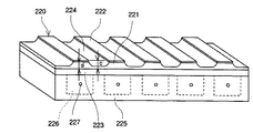
【0172】
例えば、図31に示すように、無機エレクトレットアクチュエータを液滴吐出ヘッドのアクチュエータに使用し、振動板223上にエレクトレット層221及び電極222を形成し、エレクトレット層221を溝224で不完全分割して複数の無機エレクトレットアクチュエータ220を構成した場合に、振動板223の厚みがエレクトレット層221の厚み以下であれば、エレクトレット層221の厚みをc、溝部224に対応する部分のエレクトレット層221の厚みをdとしたとき、d/cが1/2以下、好ましくは1/5以下となる溝深さに形成する。
【0173】
【発明の効果】
以上説明したように、本発明に係る液滴吐出ヘッドによれば、相互干渉の低減した微細分割駆動が可能な液滴吐出ヘッドが得られる。
【図面の簡単な説明】
【図1】請求項1の発明に係る無機エレクトレットアクチュエータの断面説明図
【図2】同無機エレクトレットアクチュエータの製造工程の一例の説明に供する説明図
【図3】図2に続く工程を説明する断面説明図
【図4】請求項3の発明に係る無機エレクトレットアクチュエータをその製造工程とともに説明する断面説明図
【図5】請求項4の発明に係る無機エレクトレットアクチュエータの説明に供する概念図
【図6】請求項5の発明に係る無機エレクトレットアクチュエータの説明に供する概念図
【図7】請求項6の発明に係る無機エレクトレットアクチュエータの製造方法の説明に供するCVD装置の概略説明図
【図8】請求項6の発明に係る無機エレクトレットアクチュエータの製造方法の説明に供するCVD装置の他の例の概略説明図
【図9】請求項7の発明に係る無機エレクトレットアクチュエータの製造方法の説明に供する断面説明図
【図10】同じく要部模式的拡大説明図
【図11】請求項8の発明に係る無機エレクトレットアクチュエータの製造方法の説明に供する説明図
【図12】図11に続く工程を説明する断面説明図
【図13】請求項9の発明に係る無機エレクトレットアクチュエータの製造方法の説明に供する説明図
【図14】請求項10の発明に係る無機エレクトレットアクチュエータの製造方法の説明に供する説明図
【図15】請求項16の発明に係る無機エレクトレットアクチュエータの製造方法の説明に供する説明図
【図16】請求項18の発明に係る無機エレクトレットアクチュエータの製造方法の説明に供する概念図
【図17】請求項22の発明に係る無機エレクトレットアクチュエータをその製造工程とともに説明する説明図
【図18】請求項23の発明に係る液滴吐出ヘッドの説明に供する断面説明図
【図19】同じく斜視説明図
【図20】請求項24の発明に係る光学デバイスの説明に供する断面説明図
【図21】同じく斜視説明図
【図22】請求項25の発明に係る光学デバイスをその製造工程とともに説明する説明図
【図23】請求項26の発明に係る圧力センサとしての書き込み入力センサの説明に供する平面説明図
【図24】同じく断面説明図
【図25】請求項29の発明に係る液滴吐出ヘッドの説明に供する説明図
【図26】請求項20の発明に係るモータの説明に供するエレクトレットモータの原理説明図
【図27】同じく誘電モータの原理説明図
【図28】同じく無機エレクトレットによる回転子の説明に供する斜視説明図
【図29】請求項31の発明に係る無機エレクトレットアクチュエータを備えた液滴吐出ヘッドの説明に供する斜視説明図
【図30】同じく断面説明図
【図31】請求項32の発明に係る無機エレクトレットアクチュエータを備えた液滴吐出ヘッドの説明に供する斜視説明図
【符号の説明】
1…エレクトレット層、2、3…電極[0001]
[Industrial application fields]
The present invention relates to an inorganic electret actuatorUsedDroplet discharge headToRelated.
[0002]
[Prior art]
Micro actuators in various micro devices such as inkjet heads and other liquid ejection heads, micro pumps, micro light modulation devices, optical devices such as optical switches, micro switches (micro relays), micro flow meters, pressure sensors, micro motors, etc. Is used.
[0003]
For example, in an inkjet head used in an inkjet recording apparatus used as an image recording apparatus (image forming apparatus) such as a printer, a facsimile, a copying apparatus, or a plotter, a diaphragm is used as an actuator unit that generates energy for pressurizing ink in the ink flow path. A piezoelectric actuator such as a piezoelectric element that deforms the electrode or an electrostatic actuator is used.
[0004]
[Problems to be solved by the invention]
By the way, as an actuator capable of performing mechanical drive, there are a piezoelectric actuator mainly composed of PZT as described above and an electrostatic actuator using an electrostatic force. The former piezoelectric actuator is made of PZT containing lead. The latter electrostatic actuator has a problem that the driving force that can be generated is not so large.
[0005]
The present invention has been made in view of the above problems, and is an inorganic electret actuator.Enables fine division drive with reduced mutual interference usingDroplet discharge headDoThe purpose is to provide.
[0006]
[Means for Solving the Problems]
To solve the above problem,The droplet discharge head according to the present invention is
In a droplet discharge head for discharging droplets,
A lead-free inorganic electret actuator is formed by forming an electret layer and an electrode obtained by subjecting an inorganic material to orientation polarization, ion polarization, and electron polarization on the diaphragm of the droplet discharge head as an actuator that generates pressure for ejecting the droplet. Configure
The vibration plate has a rigidity of 5000 to 12000 kg / mm. 2 And the thickness of the diaphragm is not more than the thickness of the electret layer and the electrode, and the thickness of the electret layer is not more than 1/5 with respect to the width of the electrode.
The configuration.
[0007]
The droplet discharge head according to the present invention is
In a droplet discharge head for discharging droplets,
A lead-free inorganic electret actuator is formed by forming an electret layer and an electrode obtained by subjecting an inorganic material to orientation polarization, ion polarization, and electron polarization on the diaphragm of the droplet discharge head as an actuator that generates pressure for ejecting the droplet. Configure
The vibration plate has a rigidity of 5000 to 12000 kg / mm. 2 And the film thickness of the diaphragm is equal to or less than the thickness of the electret layer and the electrode, and a groove is formed to divide the electret layer into a plurality of actuator parts to correspond to the groove part. The thickness of the electret layer to be ½ or less of the thickness of the electret layer
The configuration.
[0038]
DETAILED DESCRIPTION OF THE INVENTION
Embodiments of the present invention will be described below with reference to the accompanying drawings.
An embodiment of an inorganic electret actuator according to the invention of
The inorganic electret actuator includes an
[0039]
Inorganic materials are cationic, negative ionic materials, or anodic or negative molecular groups, or ionic elements or atomic groups with different electronegativity are crystallized to give an electric field and orientation polarization. The
[0040]
An example of the manufacturing process of such an inorganic electret actuator will be described with reference to FIGS.
First, as shown in FIG. 2, for example, 2MgO · 2Al of cordierite2OThree・ 5SiO2La of complex powder (average particle size 0.5 to 3 μm) and fine powder (average particle size 0.5 to 3 μm)2OThreeA
[0041]
Then, the
[0042]
Thereafter,
[0043]
Here, the basic structure of a device using this inorganic electret actuator is formed by, for example, a deformable member (hereinafter also referred to as “vibrating plate”) made of a conductive material or an insulating material coated with an electrode material. Then, this diaphragm is used as the
[0044]
In this way, by configuring the inorganic electret actuator to include an electret layer in which an inorganic material is oriented, ion-polarized, and electronically polarized, a lead-free novel actuator having high mechanical strength can be obtained.
[0045]
Next, an embodiment of an inorganic electret actuator according to the invention of
Here, the inorganic material includes a ferroelectric, a dielectric, or a solid electrolyte material, and further includes these particle-oriented ceramics. Specific materials include ZrTiOFour-SnO2TiO2, Fe2OThree-NiO, Zn2TiO2ZnNiTiOFourZnFe2OFour, K2OAl2O3-SiO2, CaOAl2O3, BaTiO3, Al2O3TiO2, MgOAl2O3There are many polarizable inorganic materials.
[0046]
Moreover, ionization and orientation polarization by a polyvalent atomic group are possible by adding a transition metal system. As a crystal structure, a spinel structure, a perovskite structure, or a sintered body is partially crystallized, and a cube, a rectangular parallelepiped, a rhombohedral, a rhombohedral, and the like exist.
[0047]
The sintering temperature depends on the combination and composition ratio of the materials, the starting material of the raw material, and the particle dependency of the material. Although it is about 200 ° C. to 1200 ° C., good results are usually obtained at 300 ° C. to 600 ° C. Although polarization inversion occurs due to hygroscopicity or strong electric field due to applied voltage, functional deterioration occurs. Under the atmosphere control conditions in this example, the material is dehydrated and in a high oxide state, and the surface electrode metal film protection ensures reliability. The lifetime is satisfied.
[0048]
As a process, it is necessary to form a strain in a part of these crystals, but a film thickness of 1 μm to 300
[0049]
Particle oriented ceramics are obtained by first sintering sintered ionic anisotropic fine powders, giving high-pressure pressing directionality, and then performing secondary pressure sintering crystallization to obtain oriented ceramics. And become polarized.
[0050]
Here again, the basic structure of a device using this inorganic electret actuator is, for example, that a diaphragm is formed of a conductive material or an insulating material with an electrode material coated on it, and this is used as the lower electrode. The inorganic material paste or sol-gel is screen printed or metal mask printed, and an inorganic oxide is formed under sintering conditions. Then, after metal mask printing or after dividing into target elements by dry or wet etching, an upper electrode is formed and sintered by printing metal paste. Voltage application and heating are simultaneously performed on the upper and lower electrodes to form inorganic electrets.
[0051]
As described above, since the inorganic material includes a ferroelectric material, a dielectric material, or a solid electrolyte material, since the material itself has a dipole moment and has a polarization orientation, a large amount of displacement can be obtained.
[0052]
Next, an embodiment of an inorganic electret actuator according to the invention of
Here, a target metal ion is selectively implanted into an inorganic material by an ion implantation apparatus to form a composition.
[0053]
In general, many organic materials are caused by corona discharge. As for organic resin materials, defects are generated in the crystal structure by electron implantation or ion implantation on the surface of various blended resins such as fluorine resin, nylon (registered trademark) 11, etc. Polarization is performed.
[0054]
In contrast, in the case of inorganic materials, the surface thermal oxide film SiO of the silicon wafer2An electret layer can be formed by irradiating an electron beam to (crystalline silicon oxide film), generating lattice defects, and forming a charge trap layer. However, an inorganic material has little crystal distortion due to electron implantation and almost no effect.
[0055]
Therefore, here, metal ions are implanted under reduced pressure. The manufacturing process of such an electret layer is demonstrated with reference to FIG.
First, when accelerating ions such as B, Sb, P, Ti, Bi, W, and Mn are implanted into the
[0056]
Furthermore, as shown in FIG. 4D, the metal ions reach 0.5 to 10 μm and are ionized by performing the sintering diffusion treatment (heat diffusion treatment). Thereby, the phase effect of crystal distortion and an ionic effect can be exhibited. And as shown to the figure (e), the
[0057]
In this way, by adopting a composition in which the target metal ions are selectively implanted into the inorganic material, the ion orientation and the polarization are increased by increasing the crystal distortion and composing the introduced multivalent ions.
[0058]
Next, an embodiment of an inorganic electret actuator according to the invention of claim 4 will be described.
Here, the inorganic material is a metal oxide (TiO2, NiO, Al2O3, Fe2O3, MnO2, Co2O3 / CoO, Sn2O3/ SnO, ZnO, etc.) and alkaline earth compound oxides (BaO, K)2O, CaO, MgO, etc.) and ZrTiO containing ferroelectrics, dielectrics, or solid electrolyte materials4-SnO2TiO2, Fe2O3-NiO, Zn2TiO2In addition, ZnNiTiO4ZnFe2O4, K2OAl2O3-SiO2, CaOAl2O3, BaTiO3, Al2O3TiO2, MgOAl2O3It is a mixed composition of polarizable inorganic materials such as.
[0059]
In particular, a compound of an alkaline earth element is a material having an element ion group as a cation and another inorganic material as a negative ion, a large crystallinity, and a high ion orientation. A highly ionic material can be obtained by controlling the redox atmosphere during firing of the composite oxide.
[0060]
The concept of this embodiment is shown in FIG. The example in the figure is an example of polarization based on the negative degree of ion groups, and orientation and polarization easily occur. In fact, Mg2Al2O4And K2SiO3, BaFe2O4Substances such as complex salts are polarized at high temperatures and electric fields.
[0061]
In this manner, by setting the inorganic material to include a metal oxide or an alkaline earth metal oxide, ion and charge polarization can be increased.
[0062]
Next, an embodiment of an inorganic electret actuator according to the invention of claim 5 will be described.
ZrTiO4-SnO2TiO2, Fe2O3-NiO, Zn2TiO2In addition, ZnNiTiO4ZnFe2O4, K2OAl2O3-SiO2, CaOAl2O3, BaTiO3, Al2O3TiO2, MgOAl2O3Polarizable inorganic materials such as non-metallic elements and SiO2, B2O3, P2O5, Sb2O5, Bi2O3) and further transition element oxides (V2O5, Cr2O3, CuO, Y2O3, Zr2O3, Nb2O3, Mo2O3, PD2O3, La2O3The composite oxide in which etc. are mixed can be easily controlled in valence depending on the firing state and atmosphere of the composite oxide containing the transition element. This can control the magnitude of crystal distortion as a result.
[0063]
A conceptual diagram of this embodiment is shown in FIG. Mixed oxides of inorganic dielectrics, polyvalent non-metallic elements, and transition elements are easily baked, especially because polyvalent atoms and transition elements have a low second ionization potential. , Orientation polarization occurs.
[0064]
As described above, by adopting a structure in which the inorganic material is a composite oxide including a transition metal oxide, unbound ions can be held in the crystal of the polyvalent element, and a large ionic polarization can be obtained.
[0065]
Next, an embodiment of a method for manufacturing an inorganic electret actuator according to the invention of claim 6 will be described.
The inorganic material can be formed by the following method.
For example, a vapor deposition method can be used. In this case, as shown in FIG. 7, for example, as shown in FIG. 7, a plasma CVD apparatus is used, for example, in a
[0066]
Alternatively, a vapor deposition method can be used. In this case, the target inorganic material or metal is heated and sublimated, an oxidizing gas is introduced into the chamber, and a film is formed by vapor deposition.
Furthermore, in the sputtering method, the metal material is a DC power source and a sputtering gas (Ar, He, N2 and O2The inorganic material having no electrical conductivity can be RF-sputtered with the same sputtering gas using a high-frequency power source.
[0067]
The CVD apparatus and the sputtering apparatus are suitable for forming a thin film, and the film growth is about 10 to 300 cm / min. In addition, the film can be easily formed while the crystal is grown by heating the substrate.
[0068]
When forming a film using any of these methods, a single layer or multiple layers are formed according to the purpose, and substrate heating and reaction gas are introduced at the time of film formation to form oxides or nitrides by plasma reaction. And control the crystallinity and amorphousness.
[0069]
In this case, since the thin film to be formed is flat, the upper electrode is then formed by a vapor deposition method or a photolithography method to form an inorganic electret layer by heating and an electric field.
[0070]
In addition, since the polarization effect is large due to the thin film, when the elements are made into multiple elements as an actuator, the mutual interference between the elements is small without dividing the elements only by individualizing the upper electrode (the electrode 2). This division step is unnecessary, and fine division is possible.
[0071]
In this way, an inorganic material is deposited on a substrate by vapor deposition or vapor deposition, and the substrate is heated and a reaction gas is introduced at the time of film formation to form an oxide or nitride to form a crystal. By forming the electret layer by controlling the property or the amorphous property, the crystallinity or the amorphous property can be easily controlled.
[0072]
Next, an embodiment of a method for manufacturing an inorganic electret actuator according to the invention of claim 7 will be described.
Here, the inorganic material is formed into a film by electrodeposition or vapor deposition, and this is anodized. Anodization oxidizes with anions with an electrode reaction. For this reason, the site portion where the electrode reacts with ions simultaneously with the formation of the oxide becomes a hole state, and the oxide becomes a porous state. As an example, the anodic oxidation product of metallic Al is well known.
[0073]
Oxide is inorganic acid used (hydrochloric acid, sulfuric acid, nitric acid, perchloric acid), inorganic acid and organic acid (formic acid, acetic acid, oxalic acid, oxalic acid), pH 1-6, the porous size in the oxide film is 50Å-3μm It can be controlled within a range. The thickness of the oxide can be regulated by controlling the voltage of the electrolysis current in the anodic oxidation reaction. In addition, metal ions necessary for polarization are added in the anodic oxidation step, and these ions are electrophoretically deposited on the oxide porous pores and taken into the oxide. A flat thin film of material is formed, and then an upper electrode is formed by vapor deposition or photolithography, and an inorganic electret layer is formed by heating and an electric field.
[0074]
In addition, since the polarization effect is large due to the thin film, when the actuator is made into multiple elements, the mutual interference between the elements is small even if the elements are not divided, only by individualizing the upper electrode, and the conventional dividing process is unnecessary. It is. When this is polarized, a large polarization orientation material is obtained.
[0075]
Here, this manufacturing process will be described with reference to FIGS.
As shown in FIG. 9A, on a
[0076]
Then, as shown in FIG. 10 (c), the
[0077]
Thereafter, metal ions of transition elements are introduced into the acid bath and electrodeposited into the
[0078]
In this way, an inorganic material is formed by electrodeposition or vapor deposition, anodized, and metal ions are electrodeposited by electrophoresis to polarize and form the electret layer, thereby forming a thin film process and controlling its crystal. Becomes easier.
[0079]
Next, an embodiment of a method for manufacturing an inorganic electret actuator according to the invention of claim 8 will be described.
Inorganic materials are mechanochemically mixed with metal oxides, alkaline earth metal oxides, or mixed materials thereof with transition metal oxides using a ball mill mixer or mortar mixer. When mixing, an organic solvent (alcohol, polyhydric alcohol, water, additives (PVA, starch) is added and pulverized with stirring particles to form a sol or gel. This is degassed and rolled into a highly viscous mass. It is formed into a sheet (green sheet) by a roller or the like.
[0080]
This is heated or combined with heating and reduced pressure degassing to form a composite oxide, formed on both sides by electrode baking or electrode screen printing, and heated and subjected to electric field treatment to obtain an inorganic electret layer.
[0081]
Here, this manufacturing process will be described with reference to FIGS.
First, as shown in FIG. 11, the sol-gel
[0082]
Next, the green sheet member obtained as described above as shown in FIG. 12A is heated and sintered to form a composite oxide, and electrodes are formed on both sides as shown in FIG. 62 and 63 are formed, subjected to heating and electric field treatment, and electretized to obtain the
[0083]
The inorganic electret actuator 60 obtained in this way is joined with an adhesive 67 on a
[0084]
Thus, an electret layer can be formed in a simple process by forming an inorganic material in a sol or gel state or forming a film into a sheet, and forming an electret layer by using heating or heating together with vacuum degassing. .
[0085]
Next, an embodiment of a method for manufacturing an inorganic electret actuator according to the invention of claim 9 will be described.
An inorganic material layer is formed, and primary baking and dehydration are performed at a low temperature. At this stage, the material is an oxide with chemically attached water, chemically bound water (hydrate). For example, there are unstable functional groups in which Si—OH, Al—OH, Fe—OH and the like are partially formed.
[0086]
Therefore, in order to perform further appropriate heat treatment on the primary fired body, an inorganic electret layer is formed and at the same time appropriate heating and an electric field are applied, and the inorganic material undergoes orientation polarization, ion polarization, and electronic polarization in the same process. At this time, the chemical composition of the inorganic material is Si—O—Si or Si═O depending on the atmospheric conditions. The dehydration becomes more complete, and the atomic group is greatly influenced by the electric field during the movement of the crystallization atomic group, and a material having a large ionic orientation, charge orientation and polarization orientation can be obtained. This electret material has improved reliability due to large polarization and scientific stabilization.
[0087]
Here, an example of this manufacturing process will be described with reference to FIG.
As shown in FIG. 2A, the inorganic material layer is fired at a low temperature of 300 to 600 ° C. to obtain a primary fired
[0088]
Thereafter, as shown in FIG. 4B,
[0089]
In this way, polarization is facilitated by simultaneously applying orientation polarization, ion polarization, and electronic polarization by forming an electret layer and simultaneously applying heating and an electric field.
[0090]
Next, an embodiment of a method for manufacturing an inorganic electret actuator according to the invention of claim 10 will be described.
By forming an inorganic material layer and performing an appropriate high-temperature heat treatment, the chemical composition of the inorganic material becomes Si—O—Si or Si═O depending on the atmospheric conditions. Dehydration is more complete, oxide formation is close to the stoichiometric composition, crystallization is progressing, and it is an oxide in a state of less hygroscopicity, deliquescence, moisture adsorption sites, and the like.
[0091]
Then, electrodes are formed on both surfaces, and then, for electretization as a secondary step, further heating and a high electric field are applied to perform orientation polarization, ion polarization, and electronic polarization. Heating and electric field have a mutual effect, and in the case of low heating, a high electric field is required, and vice versa. However, it is essential that the material has a melting point and is below that temperature.
[0092]
Here, an example of this manufacturing process will be described with reference to FIG.
As shown in FIG. 3A, the inorganic material layer is fired at a high temperature at 400 to 1200 ° C. to obtain a primary fired
[0093]
Thereafter, as shown in FIG. 4B,
[0094]
As described above, after forming the inorganic material layer, stable polarization can be performed by applying orientation polarization, ion polarization, and electronic polarization by applying heating, an electric field, and a magnetic field.
[0095]
Next, an embodiment of a method for manufacturing an inorganic electret actuator according to the invention of
Here, heating and electric field treatment are performed in pressurized air at 1 atm or higher or in an oxygen-rich pressurized state with addition of oxygen during electretization. Thereby, the thermal diffusion of oxygen is sufficient, and a compound close to the stoichiometric composition ratio of the high oxide can be obtained.
[0096]
For example, an element having a multivalent valence is Fe3O4Are divalent FeO and trivalent Fe2O3This complex oxide is not limited by adding this condition.2OThreeNear high crystallinity and high oxide.
[0097]
This is effective for increasing the anionic group's cathodicity. Furthermore, it is a high oxide as well as a high oxide at the same time, has little surface charge diffusion and transfer, has high frequency drive followability, a large electret effect, and good stability. Note that this step is performed in accordance with the description of FIG. 2 and FIG. 3 described in the embodiment of the first aspect of the invention in the heating and electric field application steps of FIG. Since heating and electric field treatment are performed in pressurized air or in an oxygen-rich pressurized state with oxygen addition, detailed description thereof is omitted.
[0098]
In this way, the material can be brought close to the stoichiometric composition by applying heating and an electric field in pressurized air or in an oxygen-rich oxygen-pressurized state during electretization, so that it becomes a peroxide. It is possible to improve reliability and functions.
[0099]
Next, an embodiment of a method for manufacturing an inorganic electret actuator according to the invention of
Here, at the time of electret treatment, heating and electric field treatment are performed in the atmosphere or oxygen-rich with oxygen addition at normal pressure. As a result, a highly stable oxide with high stability and flexibility in which oxygen diffusion is dense and crystallinity and amorphousness are mixed can be formed.
[0100]
Note that this step is performed in the air or with oxygen added as described above in the heating and electric field application steps of FIG. 3 (f) in accordance with the description of FIGS. 2 and 3 described in the embodiment of the invention of
[0101]
In this way, by applying heating and an electric field in the atmospheric state or in an oxygen-rich oxygen-enriched atmospheric state during electretization, the crystallinity is high, a high oxide is obtained, and a reproducible function is obtained. .
[0102]
Next, an embodiment of a method for manufacturing an inorganic electret actuator according to the invention of
Here, heating and electric field treatment are performed in a vacuum or a vacuum degassing state during electretization. As a result, it is possible to obtain a semiconductor material having a low internal resistance due to metal-rich crystallization and a material having a large strain deformation due to a low voltage applied electric field. In addition, the inorganic electret thus obtained can be driven at a low voltage. However, leakage occurs in high voltage driving, and heat generation and power loss occur.
[0103]
Note that this process is performed in accordance with the description of FIG. 2 and FIG. 3 described in the embodiment of the first aspect of the invention in the heating and electric field application processes of FIG. Since heating and electric field treatment are performed in a gas state, detailed description thereof is omitted.
[0104]
Thus, by applying heating and an electric field in a vacuum or reduced pressure degassing state during the electretization treatment, degassing of the reducing atmosphere and impurities and air removal between the molecular grain boundaries are possible, and the crystallinity increases. That is, the attached oxygen and weakly bonded oxygen are released, and the volatile additive is greatly reduced to obtain a complex oxide with high purity, thereby improving densification and crystallinity.
[0105]
Next, an embodiment of a method for manufacturing an inorganic electret actuator according to the invention of
Here, at the time of the electret treatment for semiconductorization, the inert gas atmosphere is heated and subjected to an electric field treatment in a gas atmosphere such as argon, helium, or nitrogen. As a result, metal materials and inorganic materials are dehydrated, internal element diffused and crystallized in the absence of anion elements, so transition elements are particularly easy to control the valence and have electrical resistance in the semi-moving region. Is obtained.
[0106]
Note that this step is also performed in the inert gas atmosphere as described above in the heating and electric field application steps of FIG. 3 (f) in accordance with the description of FIGS. 2 and 3 described in the embodiment of the invention of
[0107]
In this way, by applying heating and an electric field in an inert gas atmosphere during electretization processing, electrode oxidation disappears or oxidizes even in high-temperature processing and does not increase in resistance, and it is possible to prevent fine growth by preventing oxide grain boundary growth. Crystal lumps and thin grain boundaries (bandries) are obtained, and the crystal ratio is increased.
[0108]
Next, an embodiment of a method for manufacturing an inorganic electret actuator according to the invention of
Here, during the electretization process, hydrogen, carbon monoxide, or ammonia, alcohol, aromatic gas, ketone gas, or aldehyde gas is added as an inert gas to the inert gas, Heating and electric field treatment are performed in these atmospheres.
As a result, the reducing gas is decomposed and a deoxygenation reaction of radical hydrogen or carbon monoxide occurs. This regulates the amount and controls the deoxygenation forcibly. Furthermore, there is a reducing action, and the inorganic material becomes a semiconductor.
[0109]
Note that this step is also performed in accordance with the description of FIG. 2 and FIG. 3 described in the embodiment of the invention of
[0110]
In this way, by applying heating and an electric field in the reducing gas or organic gas addition atmosphere during the electretization treatment, it is possible to control the valence of the polyvalent element of the transition metal element, and increase the crystallinity and distortion. In addition, since the reduction is forced, a mass of fine crystals and a thin grain boundary (bundry) can be obtained by preventing the growth of oxide grain boundaries.
[0111]
Next, an embodiment of a method for manufacturing an inorganic electret actuator according to the invention of
Here, an inorganic material layer is formed using an inorganic material including a ferroelectric material, a dielectric material, or a solid electrolyte material, for example, using the manufacturing method according to the invention of claim 6, 7 or 8, and then heated. When an orientation electric field, ionic polarization, or electronic polarization is performed by applying an electric field, a sintering aid having a flux effect is added.
[0112]
This is the addition of vitreous, CuO, Bi2OThree, PbO, B2O3, Sb2O5, P2O5Or alkaline earth carbonates and nitrates, but for example CaCO3, BaCO3, K2CO3Or Ca (NO3)2, Ba (NO3)2, KNO3Etc. are added at 0.5 to 10 wt%.
[0113]
These are effective as sintering aids for inorganic materials, and can be prevented from being embrittled by lowering the crystallization temperature and containing an amorphous material (glass body), thereby achieving densification and flexibility. This promotes the improvement of the elastic modulus of the material and the development of some flexibility, 8000kg / mm2 ~ 20000kg / mm2Thus, a large driving force as a monomorph actuator can be obtained.
[0114]
The state of the crystal grain boundary in this case is shown in FIG. As shown in FIG. 5A, when no flux agent is added, there are voids (small voids) in the crystal grain boundary portion, and an amorphous body exists in the crystal grain boundary. This amount is controllable.
[0115]
Here, when a flux agent is added, as shown in FIG. 4B, glassy material is formed simultaneously with decomposition, and the material is condensed at the melted portion, thereby preventing the generation of voids. Therefore, low temperature firing becomes possible. Also in this case, an amorphous body exists in the crystal grain boundary, and embrittlement prevention and slight flexibility are exhibited.
[0116]
In this way, after forming the inorganic material layer, by applying a heating and an electric field, and adding a sintering aid having a flux effect when performing orientation polarization, ion polarization, and electronic polarization, a ferroelectric, dielectric In addition, by forming an inorganic material layer containing a solid electrolyte material and adding a sintering aid with a flux effect, it becomes easier to control the crystallinity and the grain boundary gap due to the flux effect, and sintering with good orientation polarization The body is obtained.
[0117]
Next, an embodiment of a method for manufacturing an inorganic electret actuator according to the invention of claim 17 will be described.
Again, using an inorganic material, including a ferroelectric, dielectric, or solid electrolyte material, for example, using the manufacturing process of the invention of claim 6, 7 or 8 to form an inorganic material layer, followed by heating In the case where orientation polarization, ion polarization, and electronic polarization are performed by applying an electric field, a sintering aid having a flux effect is added.
[0118]
Here, when a sintering aid having a flux (melting) effect is added and heat melting and decomposition are performed, crystallization starts at a temperature at which crystal growth does not occur in the main composite oxide. This is because when the sintering aid is heated and melted and decomposed, ions, radicals, and primary decomposition products are generated, and the chemically unstable part (functional group) on the surface of the composite oxide grain boundary of the main material is the main material. The composite oxide grain boundary surfaces react with each other to grow crystals, or form a composite salt (amorphous) glass body of the constituent material composition of the main material and the sintering aid. Thereby, the main material crystal growth and the amorphous composite oxide are formed. This can form a dense structure with high crystallinity and slight flexibility.
[0119]
Here, the composition ratio depends on the amount of sintering aid to be added and the processing temperature. That is, the range of 80% or more and 95% or less of the specific gravity relative to the composite oxide stoichiometric composition (close-packed) crystal specific gravity of the main material is reliable in terms of crystal strain, elastic modulus, denseness, and flexibility. Large actuators can be obtained.
[0120]
As described above, when the sintering aid is added, the electric field distortion depending on crystallinity is obtained by setting the crystallinity of the generated composite oxide (stoichiometric composition) specific gravity to 80% or more and 95% or less. In addition, the amorphous portion has flexibility, and cracks due to monomorph driving do not occur, and the device has high workability and can form a microfabricated device.
[0121]
Next, an embodiment of an inorganic electret actuator according to the invention of claim 18 will be described.
Again, using an inorganic material, including a ferroelectric, dielectric, or solid electrolyte material, an inorganic material layer is formed using, for example, the manufacturing process of the invention of claim 6, 7 or 8, followed by heating and An electric field is applied to perform orientation polarization, ion polarization, and electronic polarization.
[0122]
Electrode formation on the composite oxide is carried out by depositing the titanium layer as an underlayer with a vapor deposition method or a baking method including frit glass, and reacting with the elements of the composite oxide or the highly diffusible elements of the sintering aid. And ion diffusion of the electrode material is prevented. Furthermore, the adhesion is improved. Thereafter, an electrode is formed of nickel, an alloy thereof, or a noble metal material that is an electrode material. Here, the property that the chemical stability of titanium element is large is used.
[0123]
Here, an example of this actuator will be described with reference to FIG.
[0124]
Thus, by adopting a structure in which the electrode layer is formed through the titanium layer with respect to the electret layer, it is possible to prevent ion diffusion from the inorganic material, prevention of alloying, and prevention of oxidation by oxygen diffusion. An electrode can be formed on the electrode material nickel, its alloy, or a noble metal material, and the reliability is improved.
[0125]
Next, an embodiment of an inorganic electret actuator according to the invention of claim 19 will be described.
Again, using an inorganic material, including a ferroelectric, dielectric, or solid electrolyte material, an inorganic material layer is formed using, for example, the manufacturing process of the invention of claim 6, 7 or 8, followed by heating and An electric field is applied to perform orientation polarization, ion polarization, and electronic polarization.
[0126]
The composite oxide electret is effective due to the electric field strength and crystal distortion, and does not require a current. Therefore, when an electrode is formed, an electrode material is formed by a CVD method, a coating method, or an impregnation method with an insulating layer having a large dielectric constant as a base. Thereby, reaction with the element of complex oxide and the element with large diffusibility of sintering auxiliary agent can be prevented, and ion diffusion of electrode material can be prevented. This is particularly effective when the composite oxide is a material having a resistance in the semiconductor region.
[0127]
As described above, the electrode layer is formed through the insulating layer having a dielectric constant of 3 or more with respect to the electret layer, whereby the voltage drop due to the divided voltage of the applied voltage can be reduced and applied. An electric field is efficiently applied to an inorganic material, and an impurity element is blocked by an insulating layer, so that an actuator without electrode damage can be obtained.
[0128]
Next, an embodiment of an inorganic electret actuator according to the invention of claim 20 will be described.
Again, using an inorganic material, including a ferroelectric, dielectric, or solid electrolyte material, an inorganic material layer is formed using, for example, the manufacturing process of the invention of claim 6, 7 or 8, followed by heating and An electric field is applied to perform orientation polarization, ion polarization, and electronic polarization.
[0129]
When forming an electrode, a nitrogen compound such as silicon nitride or aluminum nitride which is an insulating layer is formed as a base layer. Nitride has high chemical stability, high density, and high heat resistance and moisture resistance. In addition, there is a dielectric constant, and there is little drop in electric field potential.
[0130]
As described above, the electrode layer is formed on the electret layer through silicon nitride, aluminum nitride, or other nitrogen compound layers, so that a nitrogen compound close to the stoichiometric composition can be easily formed. It can be formed and its crystal is dense, so it can prevent the diffusion of impurities, prevent the diffusion of ions from inorganic materials, prevent alloying, and also prevent the oxidation by oxygen diffusion, stable characteristics Is obtained.
[0131]
Next, an embodiment of an inorganic electret actuator according to the invention of
Although the inorganic material composite oxide depends on the size of the crystal grains, it can be a multi-element, array, or block, as well as a single drive element. Thereby, it is possible to configure a droplet discharge head such as an inkjet head using a line pressure sensor and a monomorph drive (actuator) element line arrayed one-dimensionally. Further, as a two-dimensional surface pressure sensor, a writing sensor, an input sensor, and the like can be used.
[0132]
In this way, an actuator suitable for the purpose can be configured by making the inorganic electret actuators multi-layered, arrayed, or blocked.
[0133]
Next, an embodiment of an inorganic electret actuator according to the invention of claim 22 will be described.
The film thickness of the inorganic material composite oxide can be widely adjusted to 0.5 μm to 3 μm by a manufacturing method. As a drive element for mechanically driving the monomorph, various methods can be used as a method for making a multi-layer, an array, and a block.
[0134]
For example, when dividing into 50 to 200 dpi by the sand blast method, an appropriate pattern is formed with a dry film resist, and the blast is made of a material having high hardness such as 3 to 8 μm of SiC, a pressure of 2 atm, a flow rate of 3 to 5 m / Process with s. When this method is used, the minimum is the formation of 50 μm elements, but a large number of large-area elements can be manufactured in a short time.
[0135]
In the case of dry etching, although depending on the constituent material of the inorganic material composite oxide, after formation of the resist pattern, sublimation etching is divided by RIE reaction in fluorine, chlorine and bromine. Anisotropy and isotropy are possible depending on conditions. Although this depends on the aspect ratio, an element having a thickness of 10 μm can be produced in the range of 0.5 to 1.
[0136]
In the case of a wet method, an ion dissolution etchant of an inorganic material composite oxide is used. However, it is only isotropic and is a mixture of mineral acids. A 30 μm element is common in mass production.
[0137]
Although the dicing method can be used, the width of the dicing blade is 20 μm, and there is a problem such as chipping, and the driving element is 30 μm.
[0138]
Here, an example of element division by etching will be described with reference to FIG. As shown in FIG. 6A, for example, the
[0139]
Then, as shown in FIG. 6C, etching is performed with blast, reactive ions, and reaction solution to form a predetermined resist
[0140]
As described above, the device can be efficiently formed by being multi-layered, arrayed, or blocked by the sandblasting method, the dry etching method, the wet method, or the dicing method.
[0141]
Next, an embodiment of a droplet discharge head according to the invention of claim 23 will be described. Here, an inorganic material composite oxide is arrayed and divided (blocked) to drive a diaphragm of a droplet discharge head such as an inkjet head on-demand, and droplets are ejected from corresponding nozzles. it can. The diaphragm is driven by a monomorph with an inorganic material composite oxide electret to eject droplets.
[0142]
A configuration example of an ink jet head which is such a droplet discharge head will be described with reference to FIGS.
A
[0143]
An
[0144]
In this inkjet head, ink is supplied from the
[0145]
As described above, by configuring the droplet discharge head using the inorganic electret actuator according to the present invention, it is possible to configure a droplet discharge head including an actuator that performs a novel mechanical drive.
[0146]
Next, an embodiment of an optical device according to the invention of claim 24 will be described.
Here, an inorganic material electret actuator is provided corresponding to the optical mirror surface that reflects light, and the optical mirror surface is deformed by mechanically driving this actuator, and light bending is performed corresponding to each drive element. Can be made.
[0147]
A metal electrode film serving as a common electrode is formed on an organic film or a thin film inorganic material, and an electret material is formed thereon. In this case, when a low temperature process is selected, a sol-gel containing fine crystal nuclei is applied or formed by a squeegee method. This is heated and dehydrated, and further, an electrode is formed by screen printing, metal mask vapor deposition, or the like, and sintered at an electric field of DC 300 V and heating at 250 ° C. Each monomorph drive element can be easily driven by forming a slit between adjacent elements. The optical mirror surface can be produced by vapor deposition, electrodeposition, or the like.
[0148]
An example of this optical device will be described with reference to FIGS.
In this optical device, a vibration plate (deformable member) 153 which is a lower electrode and serves as a common electrode of each actuator is provided on a
[0149]
20A shows an example in which the
[0150]
In this optical device, since the
[0151]
Thus, by configuring an optical device using the inorganic electret actuator according to the present invention, an optical device including an actuator that performs a novel mechanical drive can be configured.
[0152]
Next, an embodiment of an optical device according to the invention of claim 25 will be described.
Here, a thin film formation method is used to maintain the optical smooth surface of the base electrode, to form a drive element composed of an inorganic electret actuator, and to divide the divided drive electrode surface optically with the individual electrode surface of each element maintaining the base smooth surface. As a mirror, an optical device for bending light corresponding to each driving element is obtained.
[0153]
An example of this optical device will be described with reference to FIG.
As shown in FIG. 2A, this optical device has a silicon oxide (SiO 2) on a
[0154]
Then, an
[0155]
Thereafter, an
[0156]
In this optical device, since the
[0157]
By configuring the optical device having the electrode surface as an optical mirror in this way, the configuration is simplified.
[0158]
Next, an embodiment of a pressure sensor according to the invention of claim 26 will be described.
When the inorganic electret layer is deformed by external pressure, pyroelectric voltage generation or resistance change occurs due to internal crystal distortion in the electret layer. By detecting this voltage or resistance change, a pressure sensor that displays the external pressure as an electrical signal based on the gate voltage rise of the switching element or the change in partial pressure can be configured.
[0159]
Next, an embodiment of a pressure sensor according to the invention of claim 27 will be described. A writing sensor and a two-dimensional surface distribution pressure sensor can be configured by making multiple inorganic electrets and forming an in-plane two-dimensional pressure sensor.
[0160]
An example of a writing input sensor using the pressure sensor according to these claims 26 and 27 will be described with reference to FIGS.
In this writing input sensor, an
[0161]
In this writing input sensor, when the protective film 176 is touched with a pressure pen, the crossed portion of the
[0162]
Next, an embodiment of a transmitter according to the invention of claim 28 will be described.
Here, the elastic material (rigidity) and shape of the inorganic material electret structure can be produced freely. The material of the vibrator is not limited to organic materials, but can be made of materials and shapes with high resonance points by bonding inorganic materials, ceramic films, metal films, organic films and inorganic material films, etc. A wide range of oscillators can be configured. With organic electrets, cones and horns with high rigidity are difficult to drive, and high-frequency oscillation cannot be followed, and there is a limit.
[0163]
Next, an embodiment of a droplet discharge head according to the invention of claim 29 will be described. The thin film inorganic material electret can be freely selected to form a film of about 0.5 to 100 μm. Therefore, an inorganic electret actuator suitable for the purpose is prepared, and only individual electrodes for mechanically driving the actuator are divided into a desired size and arrayed. Thereby, without interposing and dividing (blocking) the drive element (the entire actuator), the mutual interference between adjacent bits is reduced, and a droplet discharge head that can obtain stable discharge characteristics can be configured.
[0164]
Here, an example of an inkjet head which is a droplet discharge head will be described with reference to FIG.
In this head, a
[0165]
In this case, since the plurality of
[0166]
Next, an embodiment of a motor according to the invention of claim 30 will be described.
Here, with the inorganic material electret configuration, the appropriate speed of electretization is set in the plane, or the appropriate shape is cut out and set on the rotor of the electrostatic motor, so that the rotation speed matches the frequency by the surrounding phase electric field drive An inorganic electret electrostatic motor having
[0167]
An example of this motor will be described with reference to FIGS.
First, as shown in FIG. 26, the basic configuration of an electret motor includes
[0168]
Therefore, since the inorganic
[0169]
Next, an embodiment of an inorganic electret actuator according to the invention of
When an inorganic material is flattened and only the element portion is vibrated by applying a voltage only for forming an individual electrode, or when the monomorph is driven as an actuator, the monomorph diaphragm has a rigidity of 5000 to 12000 kg / mm.2When the film thickness is less than or equal to the electret film thickness, the aspect ratio (b / a) with little mutual interference is 1/5 or less, and the mutual interference noise can be ignored is 1/8 or less. . Thereby, it is possible to perform fine division driving with reduced process deletion and mutual interference.
[0170]
For example, as shown in FIGS. 29 and 30, an
[0171]
Next, an embodiment of an inorganic electret actuator according to the invention of claim 32 will be described.
When an inorganic material is flattened to form an electret structure in which orientation polarization, ion polarization, and electron polarization are applied, multi-elements do not completely divide the element, and grooves are formed between sensor elements, using individual electrodes as a mask. Etch or cut groove with equivalent pattern. The depth of the groove is that the rigidity of the monomorph diaphragm is 5000-12000 kg / mm2In this range, the groove thickness of the film thickness and the electret film thickness is formed to be equal to or less. The thickness of the electret layer in the groove portion where the mutual interference due to the electret film thickness between the elements is small is 1/2 or less of the thickness of the electret layer, and the mutual interference noise can be ignored is 1/5 or less. Thereby, it is possible to perform fine division driving with reduced process deletion and mutual interference.
[0172]
For example, as shown in FIG. 31, an inorganic electret actuator is used as an actuator for a droplet discharge head, an
[0173]
【The invention's effect】
As explained above,According to the droplet discharge head according to the present invention,Thus, a droplet discharge head capable of fine division driving with reduced mutual interference can be obtained.
[Brief description of the drawings]
FIG. 1 is an explanatory cross-sectional view of an inorganic electret actuator according to the invention of
FIG. 2 is an explanatory diagram for explaining an example of a manufacturing process of the inorganic electret actuator
FIG. 3 is a cross-sectional explanatory diagram illustrating a process following FIG.
FIG. 4 is an explanatory cross-sectional view for explaining an inorganic electret actuator according to the invention of
FIG. 5 is a conceptual diagram for explaining an inorganic electret actuator according to the invention of claim 4;
FIG. 6 is a conceptual diagram for explaining an inorganic electret actuator according to the invention of claim 5;
FIG. 7 is a schematic explanatory view of a CVD apparatus for explaining a method for manufacturing an inorganic electret actuator according to the invention of claim 6;
FIG. 8 is a schematic explanatory diagram of another example of a CVD apparatus used to explain a method of manufacturing an inorganic electret actuator according to the invention of claim 6;
FIG. 9 is a cross-sectional explanatory diagram for explaining a method for manufacturing an inorganic electret actuator according to the invention of claim 7;
FIG. 10 is a schematic enlarged explanatory view of the main part.
FIG. 11 is an explanatory diagram for explaining a method of manufacturing an inorganic electret actuator according to the invention of claim 8;
12 is a cross-sectional explanatory diagram illustrating a process following FIG.
FIG. 13 is an explanatory diagram for explaining a method of manufacturing an inorganic electret actuator according to the invention of claim 9;
FIG. 14 is an explanatory diagram for explaining a method of manufacturing an inorganic electret actuator according to the invention of claim 10;
FIG. 15 is an explanatory diagram for explaining a method of manufacturing an inorganic electret actuator according to the invention of
FIG. 16 is a conceptual diagram for explaining a method for manufacturing an inorganic electret actuator according to the invention of claim 18;
FIG. 17 is an explanatory view for explaining an inorganic electret actuator according to the invention of claim 22 together with its manufacturing process;
FIG. 18 is a cross-sectional explanatory diagram for explaining a droplet discharge head according to the invention of claim 23;
FIG. 19 is also a perspective explanatory view
FIG. 20 is an explanatory cross-sectional view for explaining an optical device according to the invention of claim 24;
FIG. 21 is also a perspective explanatory view
FIG. 22 is an explanatory view for explaining an optical device according to the invention of claim 25 together with its manufacturing process;
FIG. 23 is an explanatory plan view for explaining a writing input sensor as a pressure sensor according to the invention of claim 26;
FIG. 24 is a cross-sectional explanatory view
FIG. 25 is an explanatory diagram for explaining a droplet discharge head according to the invention of claim 29;
FIG. 26 is a diagram illustrating the principle of an electret motor used for explaining the motor according to the invention of claim 20;
FIG. 27 is a diagram illustrating the principle of a dielectric motor.
FIG. 28 is a perspective explanatory view for explaining the rotor by the inorganic electret as well.
FIG. 29 is a perspective explanatory view for explaining a droplet discharge head including an inorganic electret actuator according to the invention of
FIG. 30 is a cross-sectional explanatory view
FIG. 31 is an explanatory perspective view for explaining a droplet discharge head including an inorganic electret actuator according to the invention of claim 32;
[Explanation of symbols]
1 ... electret layer, 2, 3 ... electrode
Claims (2)
前記液滴を吐出させる圧力を発生させるアクチュエータとして、前記液滴吐出ヘッドの振動板上に無機材料を配向分極、イオン分極、電子分極させたエレクトレット層及び電極を形成して無鉛の無機エレクトレットアクチュエータを構成し、
前記振動板の剛性が5000〜12000kg/mm 2 の範囲であって、かつ、前記振動板の膜厚が前記エレクトレット層及び電極の厚み以下で、前記電極の幅に対して前記エレクトレット層の層厚が1/5以下である
ことを特徴とする液滴吐出ヘッド。In a droplet discharge head for discharging droplets,
A lead-free inorganic electret actuator is formed by forming an electret layer and an electrode obtained by subjecting an inorganic material to orientation polarization, ion polarization, and electron polarization on the diaphragm of the droplet discharge head as an actuator that generates pressure for ejecting the droplet. Configure
The diaphragm has a rigidity in the range of 5000 to 12000 kg / mm 2 , and the thickness of the diaphragm is equal to or less than the thickness of the electret layer and the electrode, and the thickness of the electret layer with respect to the width of the electrode The droplet discharge head is characterized in that is 1/5 or less .
前記液滴を吐出させる圧力を発生させるアクチュエータとして、前記液滴吐出ヘッドの振動板上に無機材料を配向分極、イオン分極、電子分極させたエレクトレット層及び電極を形成して無鉛の無機エレクトレットアクチュエータを構成し、
前記振動板の剛性が5000〜12000kg/mm 2 の範囲であって、かつ、前記振動板の膜厚が前記エレクトレット層及び電極の厚み以下で、前記エレクトレット層を不完全分割して複数のアクチュエータ部に分割する溝が形成され、前記溝部に対応する前記エレクトレット層の厚さが前記エレクトレット層の厚さの1/2以下である
ことを特徴とする液滴吐出ヘッド。 In a droplet discharge head for discharging droplets,
A lead-free inorganic electret actuator is formed by forming an electret layer and an electrode obtained by subjecting an inorganic material to orientation polarization, ion polarization, and electron polarization on the diaphragm of the droplet discharge head as an actuator that generates pressure for ejecting the droplet. Configure
The diaphragm has a rigidity in the range of 5000 to 12000 kg / mm 2 , and the thickness of the diaphragm is equal to or less than the thickness of the electret layer and the electrode. A droplet discharge head, characterized in that a groove to be divided is formed, and a thickness of the electret layer corresponding to the groove portion is ½ or less of a thickness of the electret layer .
Priority Applications (1)
| Application Number | Priority Date | Filing Date | Title |
|---|---|---|---|
| JP2002276473A JP4138421B2 (en) | 2002-09-24 | 2002-09-24 | Droplet discharge head |
Applications Claiming Priority (1)
| Application Number | Priority Date | Filing Date | Title |
|---|---|---|---|
| JP2002276473A JP4138421B2 (en) | 2002-09-24 | 2002-09-24 | Droplet discharge head |
Publications (2)
| Publication Number | Publication Date |
|---|---|
| JP2004120809A JP2004120809A (en) | 2004-04-15 |
| JP4138421B2 true JP4138421B2 (en) | 2008-08-27 |
Family
ID=32272334
Family Applications (1)
| Application Number | Title | Priority Date | Filing Date |
|---|---|---|---|
| JP2002276473A Expired - Fee Related JP4138421B2 (en) | 2002-09-24 | 2002-09-24 | Droplet discharge head |
Country Status (1)
| Country | Link |
|---|---|
| JP (1) | JP4138421B2 (en) |
Families Citing this family (9)
| Publication number | Priority date | Publication date | Assignee | Title |
|---|---|---|---|---|
| JP4599092B2 (en) * | 2004-05-19 | 2010-12-15 | オリンパス株式会社 | Manufacturing method of electret film for electrostatic actuator |
| JP4424331B2 (en) | 2005-08-01 | 2010-03-03 | セイコーエプソン株式会社 | Electrostatic actuator, droplet discharge head, method for driving droplet discharge head, and method for manufacturing electrostatic actuator |
| JP5200746B2 (en) * | 2008-08-05 | 2013-06-05 | セイコーエプソン株式会社 | Electrostatic actuator, droplet discharge head, droplet discharge device, and method for manufacturing droplet discharge head |
| EP2936576B1 (en) | 2012-12-21 | 2017-03-15 | Canon Kabushiki Kaisha | Vibration wave driving device, image pickup device, optical apparatus, liquid discharge device, and electronic apparatus |
| JP6309283B2 (en) * | 2014-01-24 | 2018-04-11 | 学校法人 関西大学 | Electret, method for manufacturing the same, and power generation apparatus using the same |
| EP3429075B1 (en) | 2016-03-07 | 2020-10-28 | Ricoh Company, Ltd. | Element, cell, and power generation device |
| CN107741236B (en) * | 2017-02-28 | 2024-02-27 | 深圳哲恒科技有限公司 | Self-driven sensor |
| CN112295738A (en) * | 2019-07-26 | 2021-02-02 | 上海必修福企业管理有限公司 | High-temperature electret material and preparation method thereof |
| CN112210843B (en) * | 2020-09-29 | 2023-03-14 | 宜昌思创新材料科技有限公司 | Composite electret material, application thereof and melt-blown fabric |
-
2002
- 2002-09-24 JP JP2002276473A patent/JP4138421B2/en not_active Expired - Fee Related
Also Published As
| Publication number | Publication date |
|---|---|
| JP2004120809A (en) | 2004-04-15 |
Similar Documents
| Publication | Publication Date | Title |
|---|---|---|
| KR101113490B1 (en) | Piezoelectric substance, piezoelectric element, and liquid discharge head and liquid discharge apparatus using piezoelectric element | |
| TWI249437B (en) | Dielectric thin film element, piezoelectric actuator and liquid discharge head, and method for manufacturing the same | |
| KR100651046B1 (en) | Dielectric film structure, piezoelectric actuator using dielectric element film structure and ink jet head | |
| JP5164052B2 (en) | Piezoelectric element, liquid discharge head, and liquid discharge apparatus | |
| KR100978145B1 (en) | Epitaxial oxide film, piezoelectric film, piezoelectric film element, and liquid delivery head and liquid delivery apparatus using piezoelectric element | |
| JP3120260B2 (en) | Piezoelectric / electrostrictive film type element | |
| US7521845B2 (en) | Piezoelectric substance, piezoelectric element, liquid discharge head using piezoelectric element, and liquid discharge apparatus | |
| JP5241087B2 (en) | Piezoelectric body, piezoelectric element, liquid discharge head using the piezoelectric element, liquid discharge apparatus, and method for manufacturing the piezoelectric element | |
| JP5241086B2 (en) | Piezoelectric body, piezoelectric element, liquid ejection head and liquid ejection apparatus using the piezoelectric element | |
| US9180667B2 (en) | Liquid-ejecting head and liquid-ejecting apparatus | |
| JPH0549270A (en) | Piezoelectric/electrostrictive actuator | |
| JP4138421B2 (en) | Droplet discharge head | |
| JP4875827B2 (en) | Piezoelectric thin film and manufacturing method thereof, piezoelectric element including the piezoelectric thin film, ink jet head using the piezoelectric element, and ink jet recording apparatus including the ink jet head | |
| JP5121186B2 (en) | Piezoelectric body, piezoelectric element, liquid discharge head, and liquid discharge apparatus | |
| JP5131674B2 (en) | Piezoelectric body and manufacturing method thereof, piezoelectric element, liquid discharge head and liquid discharge apparatus using the same | |
| JP2005119166A (en) | Piezoelectric element, inkjet head, method of manufacturing the same, and inkjet recorder | |
| JP2002084012A (en) | Piezoelectric material film and piezoelectric material element provided therewith | |
| JP2007088445A (en) | Piezoelectric, piezoelectric element, liquid ejection head, liquid ejector and process for producing piezoelectric | |
| JP2004255614A (en) | Liquid droplet discharging head and actuator | |
| JP3592057B2 (en) | Method for manufacturing piezoelectric unit and method for manufacturing inkjet head | |
| JP3591316B2 (en) | Piezoelectric actuator, ink jet recording head, and printer | |
| JP2005144594A (en) | Actuator device, actuator, droplet discharging device, and droplet discharging head | |
| JP4078629B2 (en) | Piezoelectric thin film element | |
| JP2003347618A (en) | Piezoelectric element, ink jet head and manufacturing method of the same, and ink jet recording device | |
| JP2002043641A (en) | Piezoelectric element and ink jet recording head using the same |
Legal Events
| Date | Code | Title | Description |
|---|---|---|---|
| A621 | Written request for application examination |
Free format text: JAPANESE INTERMEDIATE CODE: A621 Effective date: 20050210 |
|
| A131 | Notification of reasons for refusal |
Free format text: JAPANESE INTERMEDIATE CODE: A131 Effective date: 20071019 |
|
| A521 | Written amendment |
Free format text: JAPANESE INTERMEDIATE CODE: A523 Effective date: 20071127 |
|
| A131 | Notification of reasons for refusal |
Free format text: JAPANESE INTERMEDIATE CODE: A131 Effective date: 20071228 |
|
| A521 | Written amendment |
Free format text: JAPANESE INTERMEDIATE CODE: A523 Effective date: 20080211 |
|
| A131 | Notification of reasons for refusal |
Free format text: JAPANESE INTERMEDIATE CODE: A131 Effective date: 20080401 |
|
| A521 | Written amendment |
Free format text: JAPANESE INTERMEDIATE CODE: A523 Effective date: 20080505 |
|
| TRDD | Decision of grant or rejection written | ||
| A01 | Written decision to grant a patent or to grant a registration (utility model) |
Free format text: JAPANESE INTERMEDIATE CODE: A01 Effective date: 20080530 |
|
| A01 | Written decision to grant a patent or to grant a registration (utility model) |
Free format text: JAPANESE INTERMEDIATE CODE: A01 |
|
| A61 | First payment of annual fees (during grant procedure) |
Free format text: JAPANESE INTERMEDIATE CODE: A61 Effective date: 20080605 |
|
| R150 | Certificate of patent or registration of utility model |
Free format text: JAPANESE INTERMEDIATE CODE: R150 |
|
| FPAY | Renewal fee payment (event date is renewal date of database) |
Free format text: PAYMENT UNTIL: 20110613 Year of fee payment: 3 |
|
| FPAY | Renewal fee payment (event date is renewal date of database) |
Free format text: PAYMENT UNTIL: 20110613 Year of fee payment: 3 |
|
| FPAY | Renewal fee payment (event date is renewal date of database) |
Free format text: PAYMENT UNTIL: 20120613 Year of fee payment: 4 |
|
| FPAY | Renewal fee payment (event date is renewal date of database) |
Free format text: PAYMENT UNTIL: 20130613 Year of fee payment: 5 |
|
| LAPS | Cancellation because of no payment of annual fees |