JP4135564B2 - Semiconductor substrate and manufacturing method thereof - Google Patents
Semiconductor substrate and manufacturing method thereof Download PDFInfo
- Publication number
- JP4135564B2 JP4135564B2 JP2003159888A JP2003159888A JP4135564B2 JP 4135564 B2 JP4135564 B2 JP 4135564B2 JP 2003159888 A JP2003159888 A JP 2003159888A JP 2003159888 A JP2003159888 A JP 2003159888A JP 4135564 B2 JP4135564 B2 JP 4135564B2
- Authority
- JP
- Japan
- Prior art keywords
- groove
- semiconductor substrate
- thermal oxide
- semiconductor
- oxide film
- Prior art date
- Legal status (The legal status is an assumption and is not a legal conclusion. Google has not performed a legal analysis and makes no representation as to the accuracy of the status listed.)
- Expired - Fee Related
Links
Images


Classifications
-
- H—ELECTRICITY
- H01—ELECTRIC ELEMENTS
- H01L—SEMICONDUCTOR DEVICES NOT COVERED BY CLASS H10
- H01L21/00—Processes or apparatus adapted for the manufacture or treatment of semiconductor or solid state devices or of parts thereof
- H01L21/70—Manufacture or treatment of devices consisting of a plurality of solid state components formed in or on a common substrate or of parts thereof; Manufacture of integrated circuit devices or of parts thereof
- H01L21/71—Manufacture of specific parts of devices defined in group H01L21/70
- H01L21/76—Making of isolation regions between components
- H01L21/763—Polycrystalline semiconductor regions
-
- H—ELECTRICITY
- H01—ELECTRIC ELEMENTS
- H01L—SEMICONDUCTOR DEVICES NOT COVERED BY CLASS H10
- H01L21/00—Processes or apparatus adapted for the manufacture or treatment of semiconductor or solid state devices or of parts thereof
- H01L21/70—Manufacture or treatment of devices consisting of a plurality of solid state components formed in or on a common substrate or of parts thereof; Manufacture of integrated circuit devices or of parts thereof
- H01L21/71—Manufacture of specific parts of devices defined in group H01L21/70
- H01L21/76—Making of isolation regions between components
- H01L21/762—Dielectric regions, e.g. EPIC dielectric isolation, LOCOS; Trench refilling techniques, SOI technology, use of channel stoppers
- H01L21/76202—Dielectric regions, e.g. EPIC dielectric isolation, LOCOS; Trench refilling techniques, SOI technology, use of channel stoppers using a local oxidation of silicon, e.g. LOCOS, SWAMI, SILO
- H01L21/76205—Dielectric regions, e.g. EPIC dielectric isolation, LOCOS; Trench refilling techniques, SOI technology, use of channel stoppers using a local oxidation of silicon, e.g. LOCOS, SWAMI, SILO in a region being recessed from the surface, e.g. in a recess, groove, tub or trench region
- H01L21/76208—Dielectric regions, e.g. EPIC dielectric isolation, LOCOS; Trench refilling techniques, SOI technology, use of channel stoppers using a local oxidation of silicon, e.g. LOCOS, SWAMI, SILO in a region being recessed from the surface, e.g. in a recess, groove, tub or trench region using auxiliary pillars in the recessed region, e.g. to form LOCOS over extended areas
-
- H—ELECTRICITY
- H01—ELECTRIC ELEMENTS
- H01L—SEMICONDUCTOR DEVICES NOT COVERED BY CLASS H10
- H01L27/00—Devices consisting of a plurality of semiconductor or other solid-state components formed in or on a common substrate
- H01L27/02—Devices consisting of a plurality of semiconductor or other solid-state components formed in or on a common substrate including semiconductor components specially adapted for rectifying, oscillating, amplifying or switching and having at least one potential-jump barrier or surface barrier; including integrated passive circuit elements with at least one potential-jump barrier or surface barrier
- H01L27/04—Devices consisting of a plurality of semiconductor or other solid-state components formed in or on a common substrate including semiconductor components specially adapted for rectifying, oscillating, amplifying or switching and having at least one potential-jump barrier or surface barrier; including integrated passive circuit elements with at least one potential-jump barrier or surface barrier the substrate being a semiconductor body
- H01L27/06—Devices consisting of a plurality of semiconductor or other solid-state components formed in or on a common substrate including semiconductor components specially adapted for rectifying, oscillating, amplifying or switching and having at least one potential-jump barrier or surface barrier; including integrated passive circuit elements with at least one potential-jump barrier or surface barrier the substrate being a semiconductor body including a plurality of individual components in a non-repetitive configuration
- H01L27/0611—Devices consisting of a plurality of semiconductor or other solid-state components formed in or on a common substrate including semiconductor components specially adapted for rectifying, oscillating, amplifying or switching and having at least one potential-jump barrier or surface barrier; including integrated passive circuit elements with at least one potential-jump barrier or surface barrier the substrate being a semiconductor body including a plurality of individual components in a non-repetitive configuration integrated circuits having a two-dimensional layout of components without a common active region
-
- H—ELECTRICITY
- H01—ELECTRIC ELEMENTS
- H01L—SEMICONDUCTOR DEVICES NOT COVERED BY CLASS H10
- H01L27/00—Devices consisting of a plurality of semiconductor or other solid-state components formed in or on a common substrate
- H01L27/02—Devices consisting of a plurality of semiconductor or other solid-state components formed in or on a common substrate including semiconductor components specially adapted for rectifying, oscillating, amplifying or switching and having at least one potential-jump barrier or surface barrier; including integrated passive circuit elements with at least one potential-jump barrier or surface barrier
- H01L27/04—Devices consisting of a plurality of semiconductor or other solid-state components formed in or on a common substrate including semiconductor components specially adapted for rectifying, oscillating, amplifying or switching and having at least one potential-jump barrier or surface barrier; including integrated passive circuit elements with at least one potential-jump barrier or surface barrier the substrate being a semiconductor body
- H01L27/08—Devices consisting of a plurality of semiconductor or other solid-state components formed in or on a common substrate including semiconductor components specially adapted for rectifying, oscillating, amplifying or switching and having at least one potential-jump barrier or surface barrier; including integrated passive circuit elements with at least one potential-jump barrier or surface barrier the substrate being a semiconductor body including only semiconductor components of a single kind
-
- H—ELECTRICITY
- H01—ELECTRIC ELEMENTS
- H01L—SEMICONDUCTOR DEVICES NOT COVERED BY CLASS H10
- H01L27/00—Devices consisting of a plurality of semiconductor or other solid-state components formed in or on a common substrate
- H01L27/02—Devices consisting of a plurality of semiconductor or other solid-state components formed in or on a common substrate including semiconductor components specially adapted for rectifying, oscillating, amplifying or switching and having at least one potential-jump barrier or surface barrier; including integrated passive circuit elements with at least one potential-jump barrier or surface barrier
- H01L27/12—Devices consisting of a plurality of semiconductor or other solid-state components formed in or on a common substrate including semiconductor components specially adapted for rectifying, oscillating, amplifying or switching and having at least one potential-jump barrier or surface barrier; including integrated passive circuit elements with at least one potential-jump barrier or surface barrier the substrate being other than a semiconductor body, e.g. an insulating body
- H01L27/1203—Devices consisting of a plurality of semiconductor or other solid-state components formed in or on a common substrate including semiconductor components specially adapted for rectifying, oscillating, amplifying or switching and having at least one potential-jump barrier or surface barrier; including integrated passive circuit elements with at least one potential-jump barrier or surface barrier the substrate being other than a semiconductor body, e.g. an insulating body the substrate comprising an insulating body on a semiconductor body, e.g. SOI
Description
【0001】
【発明の属する技術分野】
本発明は、半導体基板およびその製造方法に関するものである。
【0002】
【従来の技術】
携帯電話など小型無線情報機器の普及により、搭載される高周波回路の小型、低消費電力化、低コスト化のため、半導体基板に能動素子と受動素子を集積して、回路を1チップ化したモノリシックICの開発が進んでいる。具体的には、半導体基板に、トランジスタ、ダイオード等の能動素子と、抵抗、キャパシタ、インダクタ等の受動素子を集積して、高周波の発振器、アンプ、フィルタ等の回路を1チップ化する。
【0003】
しかしながら、半導体基板上にインダクタを形成する場合、非特許文献1に記載されているように、インダクタを構成する導電体と半導体基板との間に寄生容量及び寄生抵抗(渦電流損)が生じるという問題がある。従って、Q値の高いインダクタを得るためには、寄生容量及び寄生抵抗を低減する必要がある。
【0004】
この問題を解決する方法として非特許文献1では、半導体基板の表面のインダクタの下方に溝(空洞)を形成する方法を提案している。しかし、非特許文献1により開示された解決法には以下の2つの問題点がある。1つは、インダクタの下のシリコンをエッチングで取り除くプロセスは、従来のシリコンLSIプロセスと相いれないものであることである。第2には、上述した構造では、インダクタを空中配線構造にしているため、十分な強度が得られないという問題である。
【0005】
そこで、上述の問題を解決する手段として、特許文献1では、半導体基板の一部分に深さ20μm以上の溝を形成し、その溝に絶縁物を充填し、その絶縁物上にインダクタ等の受動素子を形成することが提案されている。これにより、インダクタを構成する導電体と半導体基板との間の寄生容量及び寄生抵抗を低減しつつ、従来のシリコンLSIプロセスとの融合を可能とし、しかも十分な強度が確保できる。
【0006】
しかしながら、特許文献1で開示されている方法では、絶縁物は有機系の絶縁性流体を用いており、以下のような問題がある。通常、このような絶縁性流体は固体化する際、体積変化(体積収縮)が起こり、能動素子を形成するための半導体基板面と受動素子を形成するための絶縁物領域面を同程度の高さにしたり絶縁物領域表面を平坦にすることが困難であるとか、体積変化により基板に応力がかかり、基板が反るという問題がある。
【0007】
また、非特許文献2,3においては次のような方法が開示されている。シリコン基板の一方の面側に深さ10μm以上の複数の溝を形成する。そして、その溝と溝とで挟まれたシリコン基板の柱(壁)を熱酸化によって完全に酸化するとともに残った溝内に酸化物を堆積させ溝を埋めることで、シリコン基板に10μm以上の厚い絶縁物領域を形成する。しかしながら、この方法においても、厚い絶縁物領域を形成した基板に能動素子を形成する場合の800℃以上の熱処理を繰り返すと、同様な不具合が発生する。つまり、シリコン基板と酸化シリコンの熱膨張係数の違い(シリコン:2.5×10⁻⁶/℃、酸化シリコン:0.5×10-6/℃)によって、シリコン基板にストレスがかかり、シリコン基板が反る。また、シリコン基板内に結晶欠陥、転位が発生し、シリコン基板領域に形成した能動素子が動作不能になる。特に、厚い絶縁物領域近傍のシリコン基板領域には、結晶欠陥、転位が集中するため、能動素子が動作不能になるのを回避するには、能動素子を厚い絶縁物領域から一定の距離(例えば数十μm)離す必要があり、その部分がデッドスペースとなり、回路の集積度を悪化させることになる。
【0008】
【特許文献1】
特開2001−77315号公報
【非特許文献1】
J.Y.C. Changらの論文“Large Suspended Inductors on Silicon and Their Use in a 2-μm CMOS RF Amplifier,”IEEE Electron Device Letters, Vol. 14, No.5, pp. 246-248 (1993)
【非特許文献2】
C.Zhangらの論文“FABRICATION OF THICK SILICON DIOXIDE LAYERS USING DRIE, OXIDATION AND TRENCH REFILL”, Technical Digest of The Fifteenth IEEE International Conference on Micro Electro Mechanical Systems, pp. 160-163 (2002)
【非特許文献3】
H. Jiangらの論文“REDUCING SILICON-SUBSTRATE PARASITICS OF ON-CHIP TRANSFORMERS”, Technical Digest of The Fifteenth IEEE International Conference on Micro Electro Mechanical Systems, pp. 649-652 (2002)
【0009】
【発明が解決しようとする課題】
本発明はこのような背景の下になされたものであり、素子機能を十分に発揮させることができ、しかも十分な強度を得ることが可能な厚い絶縁物層を有し、かつ基板の反りや結晶欠陥、転位が発生しにくく、高い集積度の回路を実現可能な半導体基板およびその製造方法を提供することを目的としている。
【0010】
【課題を解決するための手段】
請求項1に記載の半導体基板は、第1の素子が配置される部位において厚さ10μm以上の熱酸化物層が形成されるとともに、当該熱酸化物層の外周面から内方において同外周面に沿って多結晶半導体を充填した溝が形成されており、多結晶半導体を充填した溝の深さが、熱酸化物層の厚さよりも大きいことを特徴としている。よって、この厚い熱酸化物層にて素子機能を十分に発揮させることができ(例えば、受動素子に対する寄生容量及び寄生抵抗を十分に低減することができ)、しかも第1の素子を空中配線構造としていないので十分な機械的強度を得ることが可能となる。また、熱酸化物層の外周面から内方において同外周面に沿って多結晶半導体を充填した溝を形成したので、多結晶半導体が第2の素子形成工程における熱ストレスの吸収層として働くため、基板の反りや結晶欠陥、転位の発生を抑制でき、第2の素子の動作不良を防止できる。これによりデッドスペースを少なくでき、高い集積度の回路を実現することができる。
【0011】
また、多結晶半導体を充填した溝の深さが、熱酸化物層の厚さよりも大きいと、半導体基板に素子を形成する工程において、厚い熱酸化物層の領域下部まで効果的に前記熱ストレスを吸収できるので、基板の反りや結晶欠陥、転位の発生をさらに抑制することができる。
【0012】
また、請求項2に記載のように、第1の素子は受動素子であり、第2の素子は能動素子であり、特に、請求項3に記載のように、受動素子は高周波を取り扱うものである場合に適用するとよい。
【0013】
請求項4に記載の半導体基板の製造方法においては、半導体基板における第1の素子が配置される部位において、深さ10μm以上の第1の溝と、この第1の溝を形成する領域の周囲に第1の溝の溝幅よりも大きな溝幅の第2の溝が同時に形成される。そして、熱酸化により第1および第2の溝の内面から酸化膜を成長させて第1の溝においては熱酸化膜によって埋設され、第2の溝においては側壁に熱酸化膜が第3の溝を残して形成される。さらに、第3の溝に多結晶半導体が充填される。これにより、請求項1に記載の半導体基板が得られる。
【0014】
請求項5に記載の半導体基板の製造方法においては、半導体基板における第1の素子が配置される部位において、深さ10μm以上の第1の溝が隣接して複数形成されるとともに第1の溝を形成する領域の周囲に第1の溝の溝幅よりも大きな溝幅の第2の溝が同時に形成される。そして、熱酸化により第1および第2の溝の内面から酸化膜を成長させて第1の溝においては熱酸化膜によって埋設されるとともに隣接する第1の溝の間が全て熱酸化膜とされ、第2の溝においては側壁に熱酸化膜が第3の溝を残して形成される。さらに、第3の溝に多結晶半導体が充填される。これにより、請求項1に記載の半導体基板が得られる。
【0015】
この請求項4,5の発明によれば、第3の溝は、第1の溝の内部を酸化物で埋めていく時の酸化膜と半導体基板との熱膨張係数差に起因するストレスを吸収し、半導体基板部分に過大な応力が加わることが無いため、基板の反りを抑制することができる。
【0016】
請求項6に記載のように、第1の溝と第2の溝を同時に形成する工程において、第2の溝の深さを第1の溝よりも深く形成することにより、請求項1に記載の半導体基板が得られる。この請求項6に記載の発明においては、基板製造プロセスにおいて、厚い酸化物層の領域下部まで効果的に酸化膜と半導体基板との熱膨張係数の差を吸収できるので、結晶欠陥、転位、基板(ウエハ)の反りの発生をさらに抑制することができる。
【0017】
請求項7に記載のように、第3の溝に多結晶半導体を充填する工程は、半導体基板上に多結晶半導体を堆積させて第3の溝内に多結晶半導体を配した後、半導体基板の表面部に堆積した多結晶半導体を除去し、さらに、半導体基板の表面に残留した多結晶半導体を熱酸化する処理を含むようにする。このようにすると、熱酸化物層の表面部分の凹部を多結晶半導体で埋設して平坦化でき、さらにその後の熱酸化により凹部に残留した多結晶半導体が酸化され体積膨張するのでさらに表面が平坦化される。こうして形成された厚い熱酸化物層は表面が基板表面とほぼ同じ高さにすることができる。
【0018】
請求項8に記載のように、第1の溝の溝幅を「W1」、第2の溝の溝幅を「W3」、半導体基板とその熱酸化物との熱膨張係数差を「A」、熱酸化に伴なう第1の溝による熱酸化物層の最大幅を「W」、室温と最大熱酸化処理温度との温度差を「T」としたとき、
W3>{(A・W・T)/2}+W1
を満足させると、第3の溝は、熱処理中の半導体とその酸化物の熱膨張率の違いによって基板の水平方向に発生する寸法差を吸収し、熱処理中に半導体基板に加わる応力を低減し、結晶欠陥、転位、基板(ウエハ)の反りの発生を抑制することができる。
【0019】
請求項9に記載のように、第1の溝において、その溝幅に対する溝深さの寸法比であるアスペクト比が10以上であると、一般的なLSI工程の範疇で形成できる膜厚1μm程度の熱酸化工程により、安価に深さ10μm以上の厚い熱酸化物層を形成できる。
【0020】
請求項10に記載のように、第1の溝において、その溝幅に対する溝深さの寸法比であるアスペクト比が20以上であると、安価に深さ20μm以上の厚い熱酸化物層を形成でき、化合物半導体基板のように半絶縁性の基板上に形成した伝送線路並みの損失低減効果を得ることが可能となる。
【0021】
請求項11に記載のように、第1の溝において、その溝幅が1μm以下であると、第3の溝の側壁の酸化膜は1μm以下となり、より安価に厚い熱酸化物層を形成できるとともに、第2の素子形成領域の結晶欠陥の発生をより抑制できる。
【0022】
請求項12に記載のように、半導体基板としてSOI基板を用い、第1および第2の溝を形成する際に同溝がSOI基板の埋め込み酸化膜層に達していると、第2の素子形成過程の熱ストレスを溝および多結晶半導体に集中させることができ、第2の素子が形成される半導体基板領域の結晶欠陥、転位の発生をさらに抑制でき、第2の素子の動作不良を防止できる。
【0023】
請求項13に記載のように、第1の素子は受動素子であり、第2の素子は能動素子であり、特に、請求項14に記載のように、受動素子は高周波を取り扱うものである場合に適用するとよい。
【0024】
【発明の実施の形態】
以下、この発明を具体化した一実施の形態を図面に従って説明する。
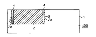
本実施形態においては、図1,2に示す半導体基板100を使用している。図1は半導体基板100の縦断面図であり、図2は半導体基板100の平面図である。図1に示すように、シリコン基板1の一方の表面側(素子形成面側)においてその一部領域に厚い熱酸化物層2が形成されている。熱酸化物層2は図2に示すように、四角形状をなしている。図1,2に示すように、熱酸化物層2の内部には溝3が形成され、この溝3は熱酸化物層2の外周面2aから内方において同外周面2aに沿って延びている。つまり、溝3は平面形状として四角環状をなしている。この溝3には多結晶シリコン(多結晶半導体)4が充填されている。即ち、熱酸化物層2の内部において熱酸化物層2の外周面2aの近傍には多結晶シリコンによる壁(4)が埋設されている。
【0025】
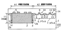
この半導体基板100を用いて図3に示す高周波モノリシックICを形成している。つまり、本実施の形態においては半導体装置として高周波モノリシックICに具体化しており、図3には高周波モノリシックICの一部分での縦断面図を示す。このモノリシックICでの半導体基板100において、厚い熱酸化物層2がその上に受動素子を配置するための絶縁物となる。
【0026】
図3では、半導体基板100に対し能動素子としてのトランジスタQ1,Q2と、受動素子としてのインダクタ5を集積化しており、高周波の発振器、アンプ、フィルタ等の回路を1チップ化している。
【0027】
詳しくは、図3において、シリコン基板1上における受動素子形成領域A1には10μm以上の厚さの熱酸化物層2が形成されており、その上には、受動素子であるスパイラルインダクタ5が形成されている。高周波回路等においてはスパイラルインダクタ5の直下では強い電磁波が発生するため、熱酸化物層2の厚さt1は10μm以上であることが好ましく、本例では30μmとしている。熱酸化物層2を構成するシリコン熱酸化膜は、比誘電率が「3.9」程度である。スパイラルインダクタ5は金属材料を用いて形成されており、本例では配線材料でもあるアルミ(Al)を用いている。ただし、材料はアルミ(Al)に限ったものではなく、Cu、Au等を用いてもよい。一方、シリコン基板1上における能動素子形成領域A2には、NチャネルMOSトランジスタQ1とPチャネルMOSトランジスタQ2が形成されている。
【0028】
図4は、酸化膜上に配置される配線(信号線路)に印加される周波数fを2GHzとしたときの、信号の伝送損失と酸化膜厚との関係を示したシミュレーション結果である。シミュレーションでは、シリコン基板の比抵抗を4Ω・cm、線路の材料をアルミ(Al)、厚さを1μm、幅を50μm、グランド配線との間隔を30μm、全長を1mmとした。
【0029】
図4から次のことが分かる。酸化膜厚が厚いほど伝送損失は小さくなるが、酸化膜厚が10μm以上であると、酸化膜厚1μmのときの10分の1程度にできる。また、酸化膜厚が20μm以上でほぼ損失は飽和している。損失が飽和する酸化膜厚は、信号の周波数、線路の抵抗値、寸法で異なってくるが、100MHz以上の高周波領域において、厚い酸化膜による伝送損失低減効果を十分に得るためには酸化膜の膜厚を10μm以上にすることが好ましい。さらに、酸化膜厚が20μm以上であれば、化合物半導体基板のように半絶縁性の基板上に形成した伝送線路並みの損失低減効果が得られる。
【0030】
次に、モノリシックICの製造プロセスを、図5,6,7,8を用いて説明する。
まず、図5(a)に示すように、シリコン基板1を用意し、その上面に酸化膜(SiO2)20を形成する。さらに、図5(b)に示すように、酸化膜20上にフォトレジスト(符号21で示す部材)を塗布する。そして、所定領域つまり受動素子形成領域A1での厚い熱酸化物層の形成予定領域に、幅1μm以下、例えば0.8μmの縞状の溝パターン22とその周囲の幅1μm以上、例えば1.6μmの溝パターン23を露光して開口させる。この時、開口した溝パターン22の間の幅W2は、溝パターン22の幅(開口部の幅)W1の81.8%程度に設定する。例えば、溝パターン22の幅(溝幅)W1が0.8μmであれば溝パターン22間の幅(溝間隔)W2を0.65μm程度に設定する。
【0031】
そして、図5(c)に示すように、前記溝パターン22,23で、酸化膜20をエッチングした後、レジスト21を除去することで、酸化膜20によるマスクを形成する。これにより、シリコン基板1の溝が形成されるべき部分が露出した状態となる。
【0032】
引き続き、図6(a)および図8の平面図に示すように、シリコン基板1における受動素子5が配置される部位(A1)において、深さ10μm以上の第1の溝24を隣接して複数形成するとともに第1の溝24を形成する領域の周囲に第1の溝24の溝幅W1よりも大きな溝幅W3の第2の溝25を同時に形成する。広義には、シリコン基板1における受動素子5が配置される部位(A1)において、深さ10μm以上の第1の溝24と、この第1の溝24を形成する領域の周囲に第1の溝24の溝幅W1よりも大きな溝幅W3の第2の溝25を同時に形成する。詳しくは次のようにする。
【0033】
異方性エッチングを用いて、シリコン基板1をエッチングして、溝24,25を同時に形成する。第1の溝24の幅W1は1μm以下であり、第2の溝25の幅W3は1μm以上であり、前述したように溝24,25の深さL1は10μm以上である。溝形成の際に、フッ素系ガスを用いた反応性イオンエッチング、特に高密度プラズマエッチングによる異方性エッチングを用いる。これにより、基板1に対してほぼ垂直な側面を有するアスペクト比(L1/W1)が「10」以上の深い溝を形成することができる。また、特開2000−299310号公報に開示されているエッチング方法を用いることにより、アスペクト比が「20」以上の深い溝を形成することも可能であり、幅1μm以下の溝幅であっても、深さは20μm以上のほぼ垂直な溝を形成することができる。また、この時、シリコン基板1における縞状の溝24の間のシリコン材料26は、その幅(厚さ)W2が溝幅W1の81.8%程度であり、高さが10μm以上の薄板状になる。
【0034】
そして、図6(b)に示すように、熱酸化により第1および第2の溝24,25の内面から酸化膜27を成長させて第1の溝24においては熱酸化膜27によって埋設するとともに隣接する第1の溝24の間を全て熱酸化膜27とし、第2の溝25においては側壁に熱酸化膜27を第3の溝3を残して形成する。広義には、熱酸化により第1および第2の溝24,25の内面から酸化膜27を成長させて第1の溝24においては熱酸化膜27によって埋設し、第2の溝25においては側壁に熱酸化膜27を第3の溝3を残して形成する。詳しくは次のようにする。
【0035】
シリコン基板1をウェットO2、スチームO2、H2およびO2混合燃焼気体中等の水素を含む酸化性雰囲気で酸化処理をする。この際、溝24,25内のシリコン基板1は酸化が進行していく時、酸化膜厚の45%に相当する厚さ分、基板内部のシリコン層が酸化シリコン化し、酸化膜厚の55%に相当する厚さ分、酸化前のシリコン基板側面より外側に膨張する。従って、酸化が進行するにつれて、縞状パターンの溝24は酸化シリコン(熱酸化膜27)で埋められていき、溝24の両側の側壁に成長した酸化膜27が互いに接触すると、その酸化膜同士で結合ができて、溝24内は酸化シリコン(熱酸化膜27)で完全に埋設できる。例えば、溝24の幅W1が0.8μmの場合では、膜厚0.73μm程度の酸化膜を成長させるのに相当する酸化処理を行うことで埋設できる。
【0036】
このような膜厚1μm以下の酸化膜27を成長させる酸化処理は通常のLSI製作工程で用いられており、1000℃以上、数時間の酸化工程で特殊な工程を必要とせず、従来技術(特許文献1)よりも安価に厚い酸化物層を形成できる。逆に、酸化膜厚2μm以上を必要とする場合には、10時間以上の酸化工程が必要となり、コスト高になるとともに、シリコン領域の結晶欠陥の発生が増加することになる。また、溝幅W1がさらに小さければ、この酸化処理はさらに短時間にでき、低コストになるとともに、最外周に形成される酸化膜厚を薄くでき、シリコン領域の結晶欠陥の発生をより抑制できる。
【0037】
なお、溝24での側面に成長した酸化膜27が互いに接触し、酸化膜同士で結合が形成される過程においては、水素の関与が必要であるため、上記のような水素を含む酸化性雰囲気での処理を行っている。しかし、この水素を含む酸化性雰囲気は酸化膜が互いに接触する直前から溝24が酸化物で完全に埋設されるまでの間のみで、それ以外の時間は水素を含まないドライO2等の酸化性雰囲気であってもよい。縞状の溝24が形成された領域内の薄板状シリコン材料26は幅(板厚)W2が溝幅W1の81.8%程度の場合には、溝24の内部が酸化物で完全に埋設されると同時に、すべて酸化され、酸化シリコン化するため、縞状の溝24を形成した領域全域に渡り、厚さが10μm以上の厚い熱酸化物層2が形成できる。
【0038】
また、厚い熱酸化物層2における基板表面付近では、酸化が基板1の表面(水平方向)とは直交する方向に進行するため、はじめにシリコンがあった部分はもり上がった状態になるため、微小な凹凸がある状態になっている。
【0039】
さらに、第2の溝25は第1の溝24よりも溝幅が大きいため第2の溝25での熱酸化により第3の溝3が残った状態となり、その溝幅Sは、初期の溝幅(第2の溝25の幅)W3が1.6μmで、W1=0.8μmの場合においては0.8μm程度となる。
【0040】
この第3の溝3は、熱処理中のシリコンと酸化シリコンの熱膨張率の違いによって基板の水平方向に発生する寸法差を吸収する。つまり、溝24の内部を酸化物で埋めていく時の酸化膜とシリコン基板との熱膨張係数の差を吸収する。これにより、熱処理中にシリコン基板1に加わる応力を低減し、結晶欠陥、転位、基板(ウエハ)の反りの発生を抑制することができる。
【0041】
この寸法差について具体的には、シリコンと酸化シリコンとの熱膨張係数差A(2.5×10⁻⁶−0.5×10-6=2.0×10⁻⁶/℃)と、熱酸化に伴なう第1の溝24による熱酸化物層2の最大幅Wと、図6(b)の酸化処理での室温と最大酸化処理温度との温度差Tとの積(A×W×T)で計算される。例えば、W=300μm、T=1100℃では、A=2.0×10-6/℃であるので、0.66μmの寸法差が生じる。従って、第2の溝25の酸化処理後の溝幅、即ち、第3の溝3の溝幅Sは少なくとも0.33(=0.66/2)μm以上残るようにしておく必要がある。
【0042】
このように、第1の溝24の溝幅を「W1」、第2の溝25の溝幅を「W3」、シリコン基板とその熱酸化物との熱膨張係数差を「A」、熱酸化に伴なう第1の溝24による熱酸化物層の最大幅を「W」、室温と最大熱酸化処理温度との温度差を「T」としたとき、
W3>{(A・W・T)/2}+W1
を満足させる。これにより、第3の溝3は、熱処理中のシリコンとその酸化物の熱膨張率の違いによって基板の水平方向に発生する寸法差を吸収し、熱処理中にシリコン基板1に加わる応力を低減し、結晶欠陥、転位、基板(ウエハ)の反りの発生を抑制することができることとなる。即ち、第3の溝3は、第1の溝24の内部を酸化物で埋めていく時の熱酸化物層とシリコン基板との熱膨張係数差に起因するストレスを吸収し、シリコン基板部分に過大な応力が加わることが無いため、基板1の反りを抑制することができる。
【0043】
なお、本工程の酸化処理は、図5(a)で形成した酸化膜(マスク材)20を残した状態で行った例を示したが、図6(b)の酸化処理の前に、酸化膜(マスク材)20をエッチングして除去した後に、酸化処理を行ってもよい。また、酸化膜(マスク材)20が窒化膜を含む膜でもよく、その場合、マスク材(20)を残して図6(b)の酸化処理を行うと、溝24,25の内面のみに酸化膜を成長させることができ、厚い熱酸化物層2の表面の凹凸を小さくできる。
【0044】
また、図6(a)の溝形成工程の後では、エッチング条件によっては、形成された溝24,25の表面がエッチング時のダメージにより微小な凹凸ができていたり、溝24,25の最上部の角部が鋭角になり、図6(b)の工程において溝面での酸化膜の成長が不均一になり、溝24内が酸化物で完全に埋設されず、空洞が残る場合がある。この空洞は、後工程のLSIプロセスに支障が無ければそのままでもよいが、場合によっては空洞にプロセス途中の薬液が残留して汚染源になったり、熱処理中に膨張して破損したりする危険性があるため、犠牲酸化工程などの溝が酸化物で埋まり易い形状に溝を整形する工程を追加してもよい。また、熱処理温度は965℃以上が好ましく、この温度以上では、酸化工程中の酸化膜の粘性流動の効果により、シリコン基板1に対して低応力で酸化膜27が形成されるとともに、溝24への酸化物の埋め込み性がよくなる。
【0045】
また、図6(b)の酸化処理において、溝24,25のアスペクト比が大きい場合には、溝24,25内に充填されている酸化処理前の雰囲気(例えば空気や窒素、アルゴンといった不活性雰囲気)が充満しているため、溝底部まで酸化性雰囲気が行き渡らず、酸化が進行しない場合がある。その場合には、図6(b)の酸化処理前に基板を真空中に挿入した後、酸素雰囲気中に挿入し、溝24,25内に酸素を充満させるとよい。
【0046】
次に、図6(c),図7(a),(b)に示す工程を経て第3の溝3に多結晶シリコン4を充填する。まず、図6(c)に示すように、シリコン基板1上に例えばLP−CVD法等により、多結晶半導体である多結晶シリコン28を1μm程度堆積して、第3の溝3内に多結晶シリコンを配する(埋設する)。また、厚い熱酸化物層2の表面の凹凸も多結晶シリコンを堆積(凹部に多結晶シリコンを埋設)させることでほぼ平坦化することができる。さらに、溝24内が酸化物で完全に埋設されず、表面に開口する空洞が残る場合においても、多結晶シリコンは空洞を埋めることができ、プロセス途中の汚染や基板の破損の危険性を排除する効果もある。
【0047】
引き続き、シリコン基板1の表面部に堆積した多結晶シリコン28を、図7(a)に示すように、例えば反応性イオンエッチング法等により厚い熱酸化物層形成予定領域以外の表面の酸化膜が露出するまでエッチング除去する。これによって、表面の余剰な多結晶シリコン28が除去され、厚い熱酸化物層2の表面の凹部と、その外周側の溝3のみに多結晶シリコンが残る形になる。
【0048】
次に、図7(b)に示すように、シリコン基板1に対し厚い熱酸化物層2の表面近傍の凹部に残った多結晶シリコンを酸化処理する。つまり、シリコン基板1の表面に残留した多結晶シリコン(28)を熱酸化する。このような工程を経て、所定領域に10μm以上の厚い熱酸化物層(厚い絶縁物層)2が形成される。また、厚い熱酸化物層2の表面部分の凹部に残留した多結晶シリコンが酸化されるとき体積膨張するのでさらに表面が平坦化される。こうして形成された厚い熱酸化物層2は、表面がシリコン基板面とほぼ同じ高さであるとともに、凹部に埋設された多結晶シリコンはほとんど酸化することが可能であるため、熱酸化物層2での表面が平坦でかつ10μm以上の厚さを有することとなる。
【0049】
以上のように形成された10μm以上の厚い熱酸化物層2の表面は、ほぼ平坦で、十分な機械的強度を有している。そのため、この半導体基板に対して、通常のLSIプロセスを用いて図3に示すようにモノリシックIC、即ち、シリコン基板1に能動素子Q1,Q2(MOSトランジスタ)を、熱酸化物層2上に受動素子(スパイラルインダクタ)5を形成することができる。つまり、シリコン基板1の表層部にPウェル領域6とNウェル領域7を形成するとともに、Pウェル領域6上においてゲート絶縁膜を介してゲート電極8を配置し、さらに、ソース領域9とドレイン領域10を形成する。同様に、Nウェル領域7上においてゲート絶縁膜を介してゲート電極11を配置するとともに、ソース領域12とドレイン領域13を形成する。その後、受動素子(スパイラルインダクタ)5を含む金属配線、さらに基板表面にパッシベーション膜14を形成する。
【0050】
ここで、通常のLSIプロセス、特に能動素子形成過程では、800℃以上の高温の熱処理工程が多数繰り返されるが、その時のシリコンと酸化シリコンの熱膨張率の違いによって基板の水平方向に発生する寸法差を多結晶シリコン4が歪むことで吸収することができる。これにより、熱処理過程にシリコン基板1に加わる応力を低減し、結晶欠陥、転位、基板(ウエハ)の反りの発生を抑制することができる。そして、シリコン基板1を低結晶欠陥、低転位にできることから能動素子の動作不良を回避でき、能動素子を熱酸化物層2に近い位置に形成できデッドスペースが少なく高い集積度の高周波モノリシックICを実現できる。また、既存のLSIの製造プロセスを変更することなく素子を形成でき、安く、大量生産に向く高性能の高周波モノリシックICを実現できる。
【0051】
このように本実施形態においては、図3での半導体基板100は、第1の素子としての受動素子5(高周波を取り扱う素子)を絶縁物の上に配置するとともに第2の素子としての能動素子Q1,Q2を作り込んだ半導体装置に用いるための半導体基板であって、受動素子5が配置される部位(A1)において厚さ10μm以上の熱酸化物層2が形成されるとともに、当該熱酸化物層2の外周面2aから内方において同外周面2aに沿って多結晶シリコン4を充填した溝3が形成されている。よって、この厚い熱酸化物層2にて素子機能を十分に発揮させることができる。具体的には、受動素子(スパイラルインダクタ)5に対する寄生容量及び寄生抵抗を十分に低減することができる。しかも受動素子5を空中配線構造としていないので十分な機械的強度を得ることが可能となる。また、熱酸化物層2の外周面2aから内方において同外周面2aに沿って多結晶シリコン4を充填した溝3を形成したので、多結晶シリコン4が能動素子Q1,Q2の形成工程における熱ストレスの吸収層として働くため、基板の反りや結晶欠陥、転位の発生を抑制でき、能動素子Q1,Q2の動作不良を防止できる。これによりデッドスペースを少なくでき、高い集積度の回路を実現することができる。
【0052】
また、図6(a)での第1の溝24において、その溝幅W1に対する溝深さL1の寸法比であるアスペクト比(L1/W1)が10以上であると、一般的なLSI工程の範疇で形成できる膜厚1μm程度の熱酸化工程により、安価に深さ10μm以上の厚い熱酸化物層2を形成できる。また、第1の溝24において、その溝幅W1に対する溝深さL1の寸法比であるアスペクト比(L1/W1)が20以上であると、安価に深さ20μm以上の厚い熱酸化物層2を形成でき、化合物半導体基板のように半絶縁性の基板上に形成した伝送線路並みの損失低減効果が得られる。
【0053】
また、第1の溝24において、その溝幅W1が1μm以下であると、第3の溝3の側壁の酸化膜は1μm以下となり、より安価に厚い熱酸化物層2を形成できるとともに、第2の素子形成領域の結晶欠陥の発生をより抑制できる。
【0054】
また、図6(a)における溝24,25の形成工程において、エッチングの条件によっては溝深さは溝幅が広いところほど深くすることができる。これを利用して、図6(a)に代わる図9(a)に示すように第1の溝24と第2の溝25を同時に形成する工程において、第2の溝25の深さL11を第1の溝24よりも深く形成する。そして、図9(b),(c)に示すように、熱酸化および多結晶シリコン28のデポを行う。この工程を経ることにより、図10に示すように、第3の溝3に充填した多結晶シリコン4の深さL12が、第1の溝24を熱酸化して埋めて形成した熱酸化物層2の厚さt1よりも大きくなるようにしてもよい。つまり、多結晶シリコン4を充填した溝3の深さL12が、熱酸化物層2の厚さt1よりも大きくなるようにしてもよい。詳しくは、溝3の深さL12を、熱酸化物層2における溝3を形成した部位以外での厚さt1よりも大きくする。これにより、半導体基板100に素子を形成する工程(LSIプロセス)において、厚い熱酸化物層2の領域下部まで効果的に熱ストレス(酸化膜とシリコン基板との熱膨張係数の差)を吸収できるので、基板内部の結晶欠陥、転位の発生、基板(ウエハ)の反りの発生をさらに抑制することができる。また、図9(a)の第2の溝25の深さL11が第1の溝24よりも深いと、半導体基板100の製造工程において、厚い熱酸化物層2の領域下部まで効果的に酸化膜とシリコン基板との熱膨張係数の差を吸収できるので、結晶欠陥、転位、基板(ウエハ)の反りの発生をさらに抑制することができる。
【0055】
これまでの説明においては一般的なシリコン基板を用いた場合を示したが、基板としては、図11に示すように、SOI(Silicon On Insulator)基板200を用いてもよい。図11において、シリコン基板201の上に厚さ1μm程度の酸化膜層202を介して厚さ10μm以上の単結晶シリコン層203が形成されている。また、単結晶シリコン層203の一部領域において熱酸化物層2が形成され、この熱酸化物層2は埋め込み酸化膜層202に達している。そのためには、図6(a)の工程の際に溝24,25が埋め込み酸化膜層202に達するまでエッチングする。即ち、溝形成工程においてSOI基板の埋め込み酸化膜層202に達する溝24,25を形成する。これにより、熱酸化物層形成予定領域のシリコン層とそれ以外の領域のシリコン層とが完全に酸化物で分離できる。そのため、その後の厚い熱酸化物層形成工程や能動素子形成過程の熱ストレスを外周部の溝3および多結晶シリコン4に集中させることができ、能動素子が形成されるシリコン基板領域の結晶欠陥、転位の発生をさらに抑制でき、能動素子の動作不良を防止できる。より具体的には、図3においては熱酸化物層2の下面部において欠陥が発生した場合には左右方向に広がっていき、能動素子形成領域でのトランジスタQ1,Q2に悪影響を及ぼす可能性がある。これに比べ、図11において埋め込み酸化膜層202の存在によりそのようなことが回避される。
【0056】
また、これまでの説明においてはトランジスタを能動素子とし、インダクタを受動素子とした場合について述べてきたが、ダイオード等を能動素子としたり、金属配線、抵抗、キャパシタ等を受動素子とした場合に適用してもよい。
【0057】
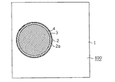
なお、図2,8においては、厚い熱酸化物層2のパターンを四角形状としているが、そのパターンは四角形状に限らず、どのようなパターンでもよい。具体的には、例えば、図12に示すように円形であっても、図13に示すように複雑な多角形等であってもよい。あるいは、図14に示すように、シリコン基板1において平面構造として熱酸化物層2が四角環状に形成されていてもよい。つまり、四角環状の熱酸化物層2の周りに単結晶シリコン1aが存在するとともに四角環状の熱酸化物層2の内側に単結晶シリコン島1bが存在するパターンでもよい。この場合には、熱酸化物層2と単結晶シリコン領域(1a,1b)との境界部分において、その熱酸化物層2の外周面2aから内方において同外周面2aに沿って多結晶シリコン4を充填した溝3が形成されている。
【0058】
さらに、これまでの説明においては、本発明による半導体基板を高周波モノリシックICに適用した例で説明した。つまり、第1の素子としての受動素子(インダクタ)5を熱酸化物層2の上に配置するとともに、第2の素子としての能動素子(トランジスタ)Q1,Q2を作り込んだ半導体装置に用いるための半導体基板であった。これに限らず、以下のようにしてもよい。
【0059】
例えば、1GHz以上のクロック周波数のマイクロプロセッサ用のICに適用する。具体的には、シリコン層に第2の素子としてのマイクロプロセッサ構成素子(トランジスタ等)を作り込むとともに熱酸化物層2の上に第1の素子として配線材を配する。
【0060】
あるいは、1000ボルト以上の高耐圧を必要とするパワー素子を具備するICに適用する。具体的には、シリコン層に第2の素子としてパワー素子を作り込むとともに熱酸化物層2にて素子分離を図り、かつ、熱酸化物層2の上に第1の素子として配線材を配する。この場合には、厚い熱酸化物層2により耐電圧性を向上させることができる。
【0061】
あるいは、基板に対して熱絶縁が必要なセンサ素子を具備するICに適用する。具体的には、熱酸化物層2の上に第1の素子としてセンサ素子を配するとともに、その横のシリコン層に第2の素子としてのセンサ信号処理回路構成素子(アンプ構成素子、A/D変換素子)を作り込む。この場合には、厚い熱酸化物層2により熱遮断性を向上させることができる。
【図面の簡単な説明】
【図1】実施の形態における半導体基板の縦断面図。
【図2】半導体基板の平面図。
【図3】実施の形態におけるモノリシックICの一部分を示す縦断面図。
【図4】信号の伝送損失と酸化膜厚についてのシミュレーション結果を示す図。
【図5】(a),(b),(c)はモノリシックICの製造プロセスを示す断面図。
【図6】(a),(b),(c)はモノリシックICの製造プロセスを示す断面図。
【図7】(a),(b)はモノリシックICの製造プロセスを示す断面図。
【図8】モノリシックICの製造プロセスを示す平面図。
【図9】(a),(b),(c)は製造プロセスを示す断面図。
【図10】半導体基板の縦断面図。
【図11】SOI基板に適用した場合のモノリシックICの一部分を示す縦断面図。
【図12】半導体基板の平面図。
【図13】半導体基板の平面図。
【図14】半導体基板を示す図。
【符号の説明】
1…シリコン基板、2…熱酸化物層、3…溝(第3の溝)、4…多結晶シリコン、5…受動素子(第1の素子)、24…第1の溝、25…第2の溝、26…シリコン材料、28…多結晶シリコン、200…SOI基板、202…埋め込み酸化膜層、A1…受動素子形成領域、Q1,Q2…能動素子。[0001]
BACKGROUND OF THE INVENTION
The present invention relates to a semiconductor substrate and a manufacturing method thereof.
[0002]
[Prior art]
Due to the spread of small wireless information devices such as mobile phones, monolithic circuits that integrate active elements and passive elements on a semiconductor substrate to reduce the size, power consumption, and cost of high-frequency circuits mounted on a single chip. IC development is progressing. Specifically, active elements such as transistors and diodes and passive elements such as resistors, capacitors, and inductors are integrated on a semiconductor substrate to form circuits such as high-frequency oscillators, amplifiers, and filters on a single chip.
[0003]
However, when the inductor is formed on the semiconductor substrate, as described in Non-Patent
[0004]
As a method for solving this problem, Non-Patent
[0005]
Therefore, as means for solving the above-mentioned problem, in
[0006]
However, the method disclosed in
[0007]
Non-Patent
[0008]
[Patent Document 1]
JP 2001-77315 A
[Non-Patent Document 1]
JYC Chang et al., “Large Suspended Inductors on Silicon and Their Use in a 2-μm CMOS RF Amplifier,” IEEE Electron Device Letters, Vol. 14, No. 5, pp. 246-248 (1993)
[Non-Patent Document 2]
C. Zhang et al. “FABRICATION OF THICK SILICON DIOXIDE LAYERS USING DRIE, OXIDATION AND TRENCH REFILL”, Technical Digest of The Fifteenth IEEE International Conference on Micro Electro Mechanical Systems, pp. 160-163 (2002)
[Non-Patent Document 3]
H. Jiang et al. "REDUCING SILICON-SUBSTRATE PARASITICS OF ON-CHIP TRANSFORMERS", Technical Digest of The Fifteenth IEEE International Conference on Micro Electro Mechanical Systems, pp. 649-652 (2002)
[0009]
[Problems to be solved by the invention]
The present invention has been made under such a background, and has a thick insulating layer that can sufficiently exhibit the element function and can obtain sufficient strength, and warps the substrate. It is an object of the present invention to provide a semiconductor substrate and a method for manufacturing the same, which are less likely to cause crystal defects and dislocations and can realize a highly integrated circuit.
[0010]
[Means for Solving the Problems]
The semiconductor substrate according to
[0011]
Also If the depth of the groove filled with the polycrystalline semiconductor is larger than the thickness of the thermal oxide layer, the thermal stress is effectively applied to the lower portion of the thick thermal oxide layer in the step of forming an element on the semiconductor substrate. Since it can absorb, generation | occurrence | production of the curvature of a board | substrate, a crystal defect, and a dislocation can further be suppressed.
[0012]
[0013]
[0014]
[0015]
This
[0016]
Claim 6 In the step of simultaneously forming the first groove and the second groove, the depth of the second groove is formed deeper than that of the first groove. 1 The semiconductor substrate described in 1 is obtained. This claim 6 In the invention described in (4), since the difference in thermal expansion coefficient between the oxide film and the semiconductor substrate can be effectively absorbed up to the lower part of the region of the thick oxide layer in the substrate manufacturing process, crystal defects, dislocations, substrate (wafer) The occurrence of warpage can be further suppressed.
[0017]
[0018]
W3> {(A · W · T) / 2} + W1
The third groove absorbs the dimensional difference generated in the horizontal direction of the substrate due to the difference in thermal expansion coefficient between the semiconductor being heat treated and its oxide, and reduces the stress applied to the semiconductor substrate during the heat treatment. Further, the occurrence of crystal defects, dislocations, and substrate (wafer) warpage can be suppressed.
[0019]
Claim 9 In the first groove, when the aspect ratio, which is the dimension ratio of the groove depth to the groove width, is 10 or more, thermal oxidation with a film thickness of about 1 μm that can be formed in the category of a general LSI process. By the process, a thick thermal oxide layer having a depth of 10 μm or more can be formed at low cost.
[0020]
[0021]
[0022]
[0023]
[0024]
DETAILED DESCRIPTION OF THE INVENTION
Hereinafter, an embodiment of the present invention will be described with reference to the drawings.
In this embodiment, the
[0025]
The
[0026]
In FIG. 3, transistors Q1 and Q2 as active elements and an
[0027]
Specifically, in FIG. 3, a
[0028]
FIG. 4 is a simulation result showing the relationship between the signal transmission loss and the oxide film thickness when the frequency f applied to the wiring (signal line) arranged on the oxide film is 2 GHz. In the simulation, the specific resistance of the silicon substrate was 4 Ω · cm, the line material was aluminum (Al), the thickness was 1 μm, the width was 50 μm, the distance from the ground wiring was 30 μm, and the total length was 1 mm.
[0029]
The following can be seen from FIG. The transmission loss decreases as the oxide film thickness increases. However, when the oxide film thickness is 10 μm or more, the transmission loss can be reduced to about 1/10 of the oxide film thickness of 1 μm. Further, the loss is almost saturated when the oxide film thickness is 20 μm or more. The oxide film thickness at which the loss is saturated differs depending on the signal frequency, the line resistance value, and the dimensions. However, in order to obtain a sufficient transmission loss reduction effect due to a thick oxide film in a high-frequency region of 100 MHz or higher, The film thickness is preferably 10 μm or more. Furthermore, when the oxide film thickness is 20 μm or more, the loss reduction effect similar to a transmission line formed on a semi-insulating substrate such as a compound semiconductor substrate can be obtained.
[0030]
Next, the manufacturing process of the monolithic IC will be described with reference to FIGS.
First, as shown in FIG. 5A, a
[0031]
Then, as shown in FIG. 5C, the
[0032]
Subsequently, as shown in the plan views of FIG. 6A and FIG. 8, a plurality of
[0033]
Using anisotropic etching, the
[0034]
Then, as shown in FIG. 6B, an
[0035]
Wet
[0036]
Such an oxidation process for growing the
[0037]
Note that, in the process in which the
[0038]
Further, in the vicinity of the substrate surface in the thick
[0039]
Furthermore, since the
[0040]
The
[0041]
Specifically, the difference in thermal expansion coefficient A (2.5 × 10 5) between silicon and silicon oxide. -6 -0.5 × 10 -6 = 2.0 × 10 -6 / ° C.), the maximum width W of the
[0042]
Thus, the groove width of the
W3> {(A · W · T) / 2} + W1
To satisfy. Thereby, the
[0043]
In addition, although the oxidation process of this process showed the example performed in the state which left the oxide film (mask material) 20 formed in FIG. 5A, the oxidation process was performed before the oxidation process of FIG. After the film (mask material) 20 is removed by etching, an oxidation treatment may be performed. Further, the oxide film (mask material) 20 may be a film including a nitride film. In that case, if the oxidation treatment of FIG. 6B is performed with the mask material (20) left, only the inner surfaces of the
[0044]
In addition, after the groove forming step of FIG. 6A, depending on the etching conditions, the surface of the formed
[0045]
6B, when the aspect ratio of the
[0046]
Next, the
[0047]
Subsequently, as shown in FIG. 7A, the
[0048]
Next, as shown in FIG. 7B, the polycrystalline silicon remaining in the recesses near the surface of the thick
[0049]
The surface of the thick
[0050]
Here, in a normal LSI process, particularly in the active element formation process, a number of heat treatment steps at a high temperature of 800 ° C. or more are repeated. The dimension generated in the horizontal direction of the substrate due to the difference in thermal expansion coefficient between silicon and silicon oxide at that time The difference can be absorbed by the distortion of the
[0051]
As described above, in the present embodiment, the
[0052]
Further, in the
[0053]
Further, in the
[0054]
In the step of forming the
[0055]
Although the case where a general silicon substrate is used has been described so far, an SOI (Silicon On Insulator)
[0056]
In the description so far, the case where the transistor is an active element and the inductor is a passive element has been described. However, the present invention is applied to a case where a diode or the like is an active element or a metal wiring, resistor, capacitor, or the like is a passive element. May be.
[0057]
In FIGS. 2 and 8, the thick
[0058]
Further, in the above description, the semiconductor substrate according to the present invention is described as an example applied to a high frequency monolithic IC. That is, the passive element (inductor) 5 as the first element is disposed on the
[0059]
For example, the present invention is applied to an IC for a microprocessor having a clock frequency of 1 GHz or more. Specifically, a microprocessor constituent element (transistor or the like) as a second element is formed in the silicon layer, and a wiring material is disposed as the first element on the
[0060]
Alternatively, it is applied to an IC having a power element that requires a high breakdown voltage of 1000 volts or more. Specifically, a power element is formed as a second element in the silicon layer, element isolation is achieved by the
[0061]
Alternatively, the present invention is applied to an IC having a sensor element that requires thermal insulation with respect to the substrate. Specifically, a sensor element is arranged as a first element on the
[Brief description of the drawings]
FIG. 1 is a longitudinal sectional view of a semiconductor substrate in an embodiment.
FIG. 2 is a plan view of a semiconductor substrate.
FIG. 3 is a longitudinal sectional view showing a part of a monolithic IC in the embodiment.
FIG. 4 is a diagram showing simulation results for signal transmission loss and oxide film thickness.
5A, 5B, and 5C are cross-sectional views showing a manufacturing process of a monolithic IC.
6A, 6B, and 6C are cross-sectional views showing a manufacturing process of a monolithic IC.
7A and 7B are cross-sectional views showing a manufacturing process of a monolithic IC.
FIG. 8 is a plan view showing a manufacturing process of the monolithic IC.
9A, 9B, and 9C are cross-sectional views showing a manufacturing process.
FIG. 10 is a longitudinal sectional view of a semiconductor substrate.
FIG. 11 is a longitudinal sectional view showing a part of a monolithic IC when applied to an SOI substrate.
FIG. 12 is a plan view of a semiconductor substrate.
FIG. 13 is a plan view of a semiconductor substrate.
FIG. 14 shows a semiconductor substrate.
[Explanation of symbols]
DESCRIPTION OF
Claims (14)
第1の素子が配置される部位(A1)において厚さ10μm以上の熱酸化物層(2)が形成されるとともに、当該熱酸化物層(2)の外周面(2a)から内方において同外周面(2a)に沿って多結晶半導体(4)を充填した溝(3)が形成されており、
前記多結晶半導体(4)を充填した溝(3)の深さ(L12)が、熱酸化物層(2)の厚さ(t1)よりも大きいことを特徴とする半導体基板。A semiconductor substrate for use in a semiconductor device in which the first element (5) is disposed on an insulator and the second element (Q1, Q2) is formed,
A thermal oxide layer (2) having a thickness of 10 μm or more is formed at a site (A1) where the first element is disposed, and the same is applied inward from the outer peripheral surface (2a) of the thermal oxide layer (2). A groove (3) filled with the polycrystalline semiconductor (4) is formed along the outer peripheral surface (2a) ,
A semiconductor substrate, wherein a depth (L12) of the groove (3) filled with the polycrystalline semiconductor (4) is larger than a thickness (t1) of the thermal oxide layer (2) .
半導体基板(1)における第1の素子(5)が配置される部位(A1)において、深さ10μm以上の第1の溝(24)と、この第1の溝(24)を形成する領域の周囲に第1の溝(24)の溝幅よりも大きな溝幅の第2の溝(25)を同時に形成する工程と、
熱酸化により前記第1および第2の溝(24,25)の内面から酸化膜(27)を成長させて第1の溝(24)においては熱酸化膜(27)によって埋設し、第2の溝(25)においては側壁に熱酸化膜(27)を第3の溝(3)を残して形成する工程と、
前記第3の溝(3)に多結晶半導体(4)を充填する工程と、
を備えたことを特徴とする半導体基板の製造方法。 A method of manufacturing a semiconductor substrate for use in a semiconductor device in which a first element (5) is disposed on an insulator and a second element (Q1, Q2) is formed,
In a portion (A1) where the first element (5) is disposed in the semiconductor substrate (1), a first groove (24) having a depth of 10 μm or more and a region for forming the first groove (24) Simultaneously forming a second groove (25) having a groove width larger than the groove width of the first groove (24) around the periphery;
An oxide film (27) is grown from the inner surfaces of the first and second grooves (24, 25) by thermal oxidation, and the first groove (24) is buried by the thermal oxide film (27), and the second Forming a thermal oxide film (27) on the side wall in the groove (25), leaving the third groove (3);
Filling the third groove (3) with a polycrystalline semiconductor (4);
A method for manufacturing a semiconductor substrate, comprising:
半導体基板(1)における第1の素子(5)が配置される部位(A1)において、深さ10μm以上の第1の溝(24)を隣接して複数形成するとともに第1の溝(24)を形成する領域の周囲に第1の溝(24)の溝幅よりも大きな溝幅の第2の溝(25)を同時に形成する工程と、 In the part (A1) where the first element (5) is disposed in the semiconductor substrate (1), a plurality of first grooves (24) having a depth of 10 μm or more are formed adjacent to each other and the first grooves (24). Simultaneously forming a second groove (25) having a groove width larger than the groove width of the first groove (24) around a region for forming
熱酸化により前記第1および第2の溝(24,25)の内面から酸化膜(27)を成長させて第1の溝(24)においては熱酸化膜(27)によって埋設するとともに隣接する第1の溝(24)の間を全て熱酸化膜(27)とし、第2の溝(25)においては側壁に熱酸化膜(27)を第3の溝(3)を残して形成する工程と、 An oxide film (27) is grown from the inner surfaces of the first and second grooves (24, 25) by thermal oxidation, and the first groove (24) is buried with the thermal oxide film (27) and adjacent to the first groove (24, 25). A step of forming a thermal oxide film (27) between the first groove (24) and forming a thermal oxide film (27) on the side wall of the second groove (25) leaving the third groove (3); ,
前記第3の溝(3)に多結晶半導体(4)を充填する工程と、 Filling the third groove (3) with a polycrystalline semiconductor (4);
を備えたことを特徴とする半導体基板の製造方法。A method for manufacturing a semiconductor substrate, comprising:
前記半導体基板(1)上に多結晶半導体(28)を堆積させて前記第3の溝(3)内に多結晶半導体(28)を配した後、前記半導体基板(1)の表面部に堆積した前記多結晶半導体(28)を除去し、さらに、前記半導体基板(1)の表面に残留した多結晶半導体(28)を熱酸化する処理を含むことを特徴とする請求項4〜6のいずれか1項に記載の半導体基板の製造方法。 Filling the third groove (3) with the polycrystalline semiconductor (4),
After depositing the polycrystalline semiconductor (28) on the semiconductor substrate (1) and arranging the polycrystalline semiconductor (28) in the third groove (3), the polycrystalline semiconductor (28) is deposited on the surface portion of the semiconductor substrate (1). 7. The method according to claim 4 , further comprising: removing the polycrystalline semiconductor (28) and further thermally oxidizing the polycrystalline semiconductor (28) remaining on the surface of the semiconductor substrate (1). A method for manufacturing a semiconductor substrate according to claim 1 .
W3>{(A・W・T)/2}+W1
を満足するようにしたことを特徴とする請求項4〜7のいずれか1項に記載の半導体基板の製造方法。 The groove width of the first groove (24) is “W1”, the groove width of the second groove (25) is “W3”, and the difference in thermal expansion coefficient between the semiconductor substrate (1) and its thermal oxide is “ A ”, when the maximum width of the thermal oxide layer by the first groove (24) accompanying thermal oxidation is“ W ”, and the temperature difference between the room temperature and the maximum thermal oxidation treatment temperature is“ T ”,
W3> {(A · W · T) / 2} + W1
The method of manufacturing a semiconductor substrate according to claim 4 , wherein the semiconductor substrate is satisfied .
Priority Applications (2)
| Application Number | Priority Date | Filing Date | Title |
|---|---|---|---|
| JP2003159888A JP4135564B2 (en) | 2002-11-12 | 2003-06-04 | Semiconductor substrate and manufacturing method thereof |
| US10/699,831 US20050012175A1 (en) | 2002-11-12 | 2003-11-04 | Semiconductor substrate and manufacturing process therefor |
Applications Claiming Priority (2)
| Application Number | Priority Date | Filing Date | Title |
|---|---|---|---|
| JP2002328605 | 2002-11-12 | ||
| JP2003159888A JP4135564B2 (en) | 2002-11-12 | 2003-06-04 | Semiconductor substrate and manufacturing method thereof |
Publications (2)
| Publication Number | Publication Date |
|---|---|
| JP2004214596A JP2004214596A (en) | 2004-07-29 |
| JP4135564B2 true JP4135564B2 (en) | 2008-08-20 |
Family
ID=32828413
Family Applications (1)
| Application Number | Title | Priority Date | Filing Date |
|---|---|---|---|
| JP2003159888A Expired - Fee Related JP4135564B2 (en) | 2002-11-12 | 2003-06-04 | Semiconductor substrate and manufacturing method thereof |
Country Status (2)
| Country | Link |
|---|---|
| US (1) | US20050012175A1 (en) |
| JP (1) | JP4135564B2 (en) |
Families Citing this family (9)
| Publication number | Priority date | Publication date | Assignee | Title |
|---|---|---|---|---|
| JP4959928B2 (en) * | 2004-09-07 | 2012-06-27 | 株式会社東芝 | Insulated gate semiconductor device |
| US7067890B2 (en) | 2004-09-29 | 2006-06-27 | Agere Systems Inc. | Thick oxide region in a semiconductor device |
| TWI279843B (en) * | 2005-09-21 | 2007-04-21 | Touch Micro System Tech | Method of fabricating microphone device and thermal oxide layer and low-stress structural layer thereof |
| US7425485B2 (en) * | 2005-09-30 | 2008-09-16 | Freescale Semiconductor, Inc. | Method for forming microelectronic assembly |
| US7264986B2 (en) * | 2005-09-30 | 2007-09-04 | Freescale Semiconductor, Inc. | Microelectronic assembly and method for forming the same |
| US7955961B2 (en) * | 2006-03-07 | 2011-06-07 | International Rectifier Corporation | Process for manufacture of trench Schottky |
| JP2009188294A (en) * | 2008-02-08 | 2009-08-20 | Nec Electronics Corp | Power mosfet |
| JP5635680B2 (en) * | 2011-03-29 | 2014-12-03 | ルネサスエレクトロニクス株式会社 | Semiconductor device and manufacturing method thereof |
| CN115995391B (en) * | 2023-03-23 | 2023-06-27 | 无锡沃达科半导体技术有限公司 | Manufacturing method of common-drain double MOSFET structure |
Family Cites Families (10)
| Publication number | Priority date | Publication date | Assignee | Title |
|---|---|---|---|---|
| US4139442A (en) * | 1977-09-13 | 1979-02-13 | International Business Machines Corporation | Reactive ion etching method for producing deep dielectric isolation in silicon |
| US4238278A (en) * | 1979-06-14 | 1980-12-09 | International Business Machines Corporation | Polycrystalline silicon oxidation method for making shallow and deep isolation trenches |
| US4571819A (en) * | 1984-11-01 | 1986-02-25 | Ncr Corporation | Method for forming trench isolation structures |
| US4910165A (en) * | 1988-11-04 | 1990-03-20 | Ncr Corporation | Method for forming epitaxial silicon on insulator structures using oxidized porous silicon |
| US5548150A (en) * | 1993-03-10 | 1996-08-20 | Kabushiki Kaisha Toshiba | Field effect transistor |
| US5726084A (en) * | 1993-06-24 | 1998-03-10 | Northern Telecom Limited | Method for forming integrated circuit structure |
| US5736749A (en) * | 1996-11-19 | 1998-04-07 | Lucent Technologies Inc. | Integrated circuit device with inductor incorporated therein |
| JP4136145B2 (en) * | 1998-12-25 | 2008-08-20 | 富士通株式会社 | Manufacturing method of semiconductor device |
| JP4005762B2 (en) * | 1999-06-30 | 2007-11-14 | 株式会社東芝 | Integrated circuit device and manufacturing method thereof |
| US6245600B1 (en) * | 1999-07-01 | 2001-06-12 | International Business Machines Corporation | Method and structure for SOI wafers to avoid electrostatic discharge |
-
2003
- 2003-06-04 JP JP2003159888A patent/JP4135564B2/en not_active Expired - Fee Related
- 2003-11-04 US US10/699,831 patent/US20050012175A1/en not_active Abandoned
Also Published As
| Publication number | Publication date |
|---|---|
| JP2004214596A (en) | 2004-07-29 |
| US20050012175A1 (en) | 2005-01-20 |
Similar Documents
| Publication | Publication Date | Title |
|---|---|---|
| US6274920B1 (en) | Integrated inductor device and method for fabricating the same | |
| JP3957038B2 (en) | Semiconductor substrate and manufacturing method thereof | |
| KR100881065B1 (en) | Monolithic low dielectric constant platform for passive components and method | |
| JP5473182B2 (en) | Semiconductor device and method having reduced capacity relative to substrate | |
| JP2003179148A (en) | Semiconductor substrate and manufacturing method therefor | |
| US7276425B2 (en) | Semiconductor device and method of providing regions of low substrate capacitance | |
| US8956949B2 (en) | Electrical signal isolation in semiconductor structures | |
| US7670926B2 (en) | Method for forming shallow trench isolation utilizing two filling oxide layers | |
| JP4135564B2 (en) | Semiconductor substrate and manufacturing method thereof | |
| US6383889B2 (en) | Semiconductor device having improved parasitic capacitance and mechanical strength | |
| JP2011233807A (en) | Semiconductor device and manufacturing method therefor | |
| KR101035393B1 (en) | Semiconductor device and method for manufacturing the same | |
| US10923577B2 (en) | Cavity structures under shallow trench isolation regions | |
| US8501578B2 (en) | Semiconductor structure formed without requiring thermal oxidation | |
| JP2001223331A (en) | Semiconductor device and manufacturing method therefor | |
| GB2345578A (en) | A method of manufacturing a semiconductor device including a trench | |
| JP2006041292A (en) | Inductance element, manufacturing method thereof and semiconductor device | |
| KR100687854B1 (en) | Method for forming the Isolation Layer of Semiconductor Device | |
| US20220320147A1 (en) | Fabrication method of fin transistor | |
| KR100304360B1 (en) | Integrated device having air-gap trench in substrate and method for forming the same | |
| JP2000269317A (en) | Semiconductor device and its manufacture | |
| KR100477547B1 (en) | Method for forming inductor of semiconductor device | |
| JPH09162285A (en) | Semiconductor device and manufacture thereof | |
| US20070114579A1 (en) | Method for integrally forming a damascene gate structure and a resistive device | |
| KR100733702B1 (en) | Semiconductor device and a method of fabricating thereof |
Legal Events
| Date | Code | Title | Description |
|---|---|---|---|
| A621 | Written request for application examination |
Free format text: JAPANESE INTERMEDIATE CODE: A621 Effective date: 20050616 |
|
| A977 | Report on retrieval |
Free format text: JAPANESE INTERMEDIATE CODE: A971007 Effective date: 20071030 |
|
| A131 | Notification of reasons for refusal |
Free format text: JAPANESE INTERMEDIATE CODE: A131 Effective date: 20071204 |
|
| A521 | Request for written amendment filed |
Free format text: JAPANESE INTERMEDIATE CODE: A523 Effective date: 20080131 |
|
| TRDD | Decision of grant or rejection written | ||
| A01 | Written decision to grant a patent or to grant a registration (utility model) |
Free format text: JAPANESE INTERMEDIATE CODE: A01 Effective date: 20080513 |
|
| A01 | Written decision to grant a patent or to grant a registration (utility model) |
Free format text: JAPANESE INTERMEDIATE CODE: A01 |
|
| A61 | First payment of annual fees (during grant procedure) |
Free format text: JAPANESE INTERMEDIATE CODE: A61 Effective date: 20080526 |
|
| R150 | Certificate of patent or registration of utility model |
Free format text: JAPANESE INTERMEDIATE CODE: R150 |
|
| FPAY | Renewal fee payment (event date is renewal date of database) |
Free format text: PAYMENT UNTIL: 20110613 Year of fee payment: 3 |
|
| FPAY | Renewal fee payment (event date is renewal date of database) |
Free format text: PAYMENT UNTIL: 20110613 Year of fee payment: 3 |
|
| FPAY | Renewal fee payment (event date is renewal date of database) |
Free format text: PAYMENT UNTIL: 20120613 Year of fee payment: 4 |
|
| FPAY | Renewal fee payment (event date is renewal date of database) |
Free format text: PAYMENT UNTIL: 20120613 Year of fee payment: 4 |
|
| FPAY | Renewal fee payment (event date is renewal date of database) |
Free format text: PAYMENT UNTIL: 20130613 Year of fee payment: 5 |
|
| FPAY | Renewal fee payment (event date is renewal date of database) |
Free format text: PAYMENT UNTIL: 20140613 Year of fee payment: 6 |
|
| R250 | Receipt of annual fees |
Free format text: JAPANESE INTERMEDIATE CODE: R250 |
|
| R250 | Receipt of annual fees |
Free format text: JAPANESE INTERMEDIATE CODE: R250 |
|
| R250 | Receipt of annual fees |
Free format text: JAPANESE INTERMEDIATE CODE: R250 |
|
| LAPS | Cancellation because of no payment of annual fees |