JP4133166B2 - Nonvolatile semiconductor memory device - Google Patents
Nonvolatile semiconductor memory device Download PDFInfo
- Publication number
- JP4133166B2 JP4133166B2 JP2002278905A JP2002278905A JP4133166B2 JP 4133166 B2 JP4133166 B2 JP 4133166B2 JP 2002278905 A JP2002278905 A JP 2002278905A JP 2002278905 A JP2002278905 A JP 2002278905A JP 4133166 B2 JP4133166 B2 JP 4133166B2
- Authority
- JP
- Japan
- Prior art keywords
- memory device
- semiconductor memory
- write
- flag
- power supply
- Prior art date
- Legal status (The legal status is an assumption and is not a legal conclusion. Google has not performed a legal analysis and makes no representation as to the accuracy of the status listed.)
- Expired - Lifetime
Links
Images


Classifications
-
- G—PHYSICS
- G11—INFORMATION STORAGE
- G11C—STATIC STORES
- G11C16/00—Erasable programmable read-only memories
- G11C16/02—Erasable programmable read-only memories electrically programmable
- G11C16/06—Auxiliary circuits, e.g. for writing into memory
- G11C16/34—Determination of programming status, e.g. threshold voltage, overprogramming or underprogramming, retention
- G11C16/3404—Convergence or correction of memory cell threshold voltages; Repair or recovery of overerased or overprogrammed cells
- G11C16/3409—Circuits or methods to recover overerased nonvolatile memory cells detected during erase verification, usually by means of a "soft" programming step
-
- G—PHYSICS
- G11—INFORMATION STORAGE
- G11C—STATIC STORES
- G11C16/00—Erasable programmable read-only memories
- G11C16/02—Erasable programmable read-only memories electrically programmable
- G11C16/06—Auxiliary circuits, e.g. for writing into memory
- G11C16/22—Safety or protection circuits preventing unauthorised or accidental access to memory cells
- G11C16/225—Preventing erasure, programming or reading when power supply voltages are outside the required ranges
-
- G—PHYSICS
- G11—INFORMATION STORAGE
- G11C—STATIC STORES
- G11C16/00—Erasable programmable read-only memories
- G11C16/02—Erasable programmable read-only memories electrically programmable
- G11C16/06—Auxiliary circuits, e.g. for writing into memory
- G11C16/30—Power supply circuits
-
- G—PHYSICS
- G11—INFORMATION STORAGE
- G11C—STATIC STORES
- G11C16/00—Erasable programmable read-only memories
- G11C16/02—Erasable programmable read-only memories electrically programmable
- G11C16/06—Auxiliary circuits, e.g. for writing into memory
- G11C16/34—Determination of programming status, e.g. threshold voltage, overprogramming or underprogramming, retention
- G11C16/3404—Convergence or correction of memory cell threshold voltages; Repair or recovery of overerased or overprogrammed cells
-
- G—PHYSICS
- G11—INFORMATION STORAGE
- G11C—STATIC STORES
- G11C11/00—Digital stores characterised by the use of particular electric or magnetic storage elements; Storage elements therefor
- G11C11/56—Digital stores characterised by the use of particular electric or magnetic storage elements; Storage elements therefor using storage elements with more than two stable states represented by steps, e.g. of voltage, current, phase, frequency
- G11C11/5621—Digital stores characterised by the use of particular electric or magnetic storage elements; Storage elements therefor using storage elements with more than two stable states represented by steps, e.g. of voltage, current, phase, frequency using charge storage in a floating gate
Landscapes
- Engineering & Computer Science (AREA)
- Computer Security & Cryptography (AREA)
- Read Only Memory (AREA)
Description
【0001】
【発明の属する技術分野】
この発明は、記憶情報を電気的に書込み、消去可能な不揮発性半導体記憶装置における書込みまたは消去動作中に電源遮断が発生した場合の対策技術に関し、例えばデータを所定の単位で一括消去可能なフラッシュメモリに利用して有効な技術に関するものである。
【0002】
【従来の技術】
フラッシュメモリは、コントロールゲートおよびフローティングゲートを有する2重ゲート構造のMOSFETからなる不揮発性記憶素子をメモリセルに使用しており、フローティングゲートの蓄積電荷量を変えることでMOSFETのしきい値電圧を変化させ情報を記憶するようにしている。
【0003】
かかるフラッシュメモリにおいては、メモリセルへの書込み・消去動作の際にしきい値電圧を低い状態に変化させることがある。この場合、メモリセルの特性バラツキによってしきい値電圧の変化の仕方にばらつきがあり、しきい値電圧が0V以下に下がってしまう(以下、デプリート状態と称する)ことがある。通常、このようにしきい値電圧が下がり過ぎたメモリセルは書上げもしくは書戻しと呼ばれる動作でしきい値電圧が所定の範囲に入るようにされる。
【0004】
【発明が解決しようとする課題】
しかしながら、メモリカードなどに使用されるフラッシュメモリにあっては、停電の発生やユーザーがカードをスロットから引き抜くことで書込みや消去動作の途中で電源が遮断されることがある。そのため、電源遮断によりメモリアレイ内の一部のメモリセルがデプリート状態のままになるおそれがある。かかるデプリート状態のメモリセルが発生すると、図3のように複数のメモリセルMCがビット線BLとソース線SLとの間に並列に接続されてなるいわゆるAND型やNOR型のフラッシュメモリにあっては、選択されていないデプリート状態のメモリセルを通して電流が流れてしまい、選択メモリセルの記憶データを正確に読み出すことができないデプリート不良が発生する。
【0005】
そして、デプリート不良を起したメモリセルを含むブロックが、メモリ上のファイルの位置を管理するテーブルデータやフォーマット情報などシステムにとって重要なデータを記憶するシステム領域として使用されていた場合には、メモリの認識ができなくなったりシステムの正常動作が不能になるおそれがある。
【0006】
この発明の目的は、フラッシュメモリのような電気的に書込み、消去可能な不揮発性半導体記憶装置において、書込みまたは消去動作中に電源遮断が発生した場合にも、デプリート状態のメモリセルが発生しないようにすることにある。
【0007】
この発明の他の目的は、フラッシュメモリのような電気的に書込み、消去可能な不揮発性半導体記憶装置において、書込みまたは消去動作中に電源遮断が発生した場合には、電源遮断が発生したことを外部装置が認識できるようにすることにある。
【0008】
この発明のさらに他の目的は、フラッシュメモリのような電気的に書込み、消去可能な不揮発性半導体記憶装置において、書込みまたは消去動作中の電源遮断により、メモリの認識ができなくなったりシステムの正常動作が不能になるのを回避できるようにすることにある。
【0009】
この発明の前記ならびにほかの目的と新規な特徴は、本明細書の記述及び添付図面から明らかになるであろう。
【0010】
【課題を解決するための手段】
本願において開示される発明のうち代表的なものの概要を簡単に説明すれば、下記のとおりである。
【0011】
すなわち、本願の第1の発明は、フラッシュメモリのような不揮発性半導体記憶装置において、書込みまたは消去動作中に電源遮断が発生した場合には、実行中の動作を中断してしきい値電圧を高くする方向へ変化させる書戻し処理を行なうように構成したものである。
【0012】
上記した手段によれば、書込みまたは消去の動作が完全に終了する前に電源遮断が発生してデプリート状態のメモリセルが発生しても、その後の書戻し処理でメモリセルのしきい値電圧が高くされるため、ブロック全体のデータが正しく読めなくなる事態に至るのを回避できるようになる。
【0013】
また、本願の他の発明は、フラッシュメモリのような不揮発性半導体記憶装置において、少なくとも書込みまたは消去動作中に電源遮断が発生した場合には、電源遮断が発生したことを外部へ知らせるフラグを設けるようにした。また、望ましくは、電源遮断時にアクセスしていたアドレスを出力する機能を設ける。これにより、ホストCPUなどの外部装置は、電源遮断で破損したメモリ内のデータの修復を行なうことができるようになる。
【0014】
本願のさらに他の発明は、フラッシュメモリのような不揮発性半導体記憶装置において、書込みまたは消去動作中に電源遮断が発生した場合には、実行中の動作を中断してしきい値電圧を高くする方向へ変化させる書戻し処理を行なうとともに、該書戻し処理が行なえるように電源電圧のレベルに応じて内部電源回路(チャージポンプの段数)を切替え可能に構成したものである。これにより、電源遮断によって電源電圧が低下しても内部電源回路がそれに応じて動作電圧を発生することによって、書戻し処理を確実に実行することができるようになる。
【0015】
【発明の実施の形態】
以下、本発明の一実施例を、図面を用いて説明する。
【0016】
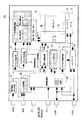
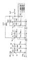
図1は、本発明を適用して有効な不揮発性半導体記憶装置の一例としてのフラッシュメモリの実施例のブロック図を示す。フラッシュメモリには1つのメモリセルに1ビットのデータを記憶可能な2値メモリがあるが、この実施例のフラッシュメモリは1つのメモリセルに2ビットのデータを記憶可能な4値メモリとして構成され、単結晶シリコンのような1個の半導体チップ上に形成される。
【0017】
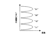
図1において、符号10は複数の不揮発性記憶素子(メモリセル)がマトリックス状に配置されたメモリアレイ、11はアドレス(Xアドレス)信号をデコードして前記メモリアレイ10内の対応するワード線WLを選択レベルにするアドレスデコーダで、該アドレスデコーダ11にはワード線WLを選択レベルに駆動するワードドライバ回路が含まれている。メモリアレイ10を構成するメモリセルは、フローティングゲートとコントロールゲートを有するMOSFETからなり、フローティングゲートに注入される電荷の量に応じてしきい値電圧が図2に示すように、4段階のいずかに設定されることにより2ビットの情報を記憶するようにされる。
【0018】
特に制限されるものでないが、本実施例においては、しきい値電圧が最も高い状態がデータ“01”に対応し、しきい値電圧が2番目に高い状態がデータ“00”、しきい値電圧が3番目に高い状態がデータ“10”、しきい値電圧が最も低い状態がデータ“11”に対応されている。なお、本明細書においては、しきい値電圧が最も低い状態を消去状態と称する。つまり、しきい値電圧を下げる動作を消去と称し、しきい値電圧を上げる動作を書込みもしくは書戻しと称する。本実施例のフラッシュメモリにおいては、メモリアレイ10内のデータを書き換える際に、メモリセルは一旦消去状態にされてからデータに相当するしきい値電圧になるように書込み電圧の印加が行なわれる。
【0019】
図1において、符号12はメモリアレイ10内のビット線BLに接続され書込みデータを保持したり読出し信号の増幅およびラッチを行なうセンスアンプ、13は1本のワード線に接続された複数のメモリセルのうちバイト単位で書込みデータや読出しデータを選択するYゲート(カラムスイッチ)、14はセンスアンプ12により増幅されたデータ信号または外部から入力された書き込みデータ信号を増幅するメインアンプ、15はメインアンプ14における信号の方向を制御したり外部からのアドレス信号に基づいてもしくは内部でアドレス信号を生成してYゲート13を選択制御したりするアクセス制御回路である。
【0020】
また、16は外部から入出力端子I/O0〜I/O7を介して入力されたコマンドコードに従って内部の制御信号を生成する制御論理部、17は該制御論理部16の制御シーケンスをマイクロプログラムのような形式で記憶するシーケンス用ROMである。入出力端子I/O0〜I/O7は、上記コマンドの入力の他、書込みデータやアドレスの入力、リードデータの出力にも利用される。書込み時に外部より入出力端子I/O0〜I/O7に入力されたライトデータは前記メインアンプ14およびセンスアンプ12を経てメモリアレイ10に供給され、ライトアドレスは一旦制御論理部16に取り込まれ電圧変換回路18にてレベル変換されてからアドレスデコーダ11に供給される。電圧変換回路18は、制御論理部16からアドレスデコーダ11に供給される書込みパルス幅(=書込み電圧を印加する時間)や書込み電圧レベルを指定する制御信号もレベル変換する。
【0021】
さらに、制御論理部16は、書込みや消去が成功したか失敗したかを示すビットなどを有するステータスレジスタSTRやアクセス中のアドレスを保持するアドレスレジスタADRを備えており、ステータスレジスタSTRやアドレスレジスタADRの内容は入出力端子I/O0〜7からチップ外部へ出力可能に構成されている。ステータスレジスタSTRには、消去結果を示すビット(消去チェックビット)、書込み結果を示すビット(書込みチェックビット)のほか、チップの内部制御状態を示すビット(以下、R/Bビット)や、後述の動作チェックフラグとして用いられるビットが設けられている。R/Bビットは、それが論理“0”のときはチップが動作状態にあり外部からのアクセスが不能であることを、また“1”のときは、チップ内部は待機状態にあって外部からのアクセスが可能であることを表わすようにされる。
【0022】
この実施例のフラッシュメモリには、特に制限されないが、電源電圧VCCのレベルを検出する電源電圧検出回路19や該電源電圧検出回路19による電源電圧の立ち上がり検出信号と外部のコントローラから入力されるリセット信号/RESに基づいて制御論理部16に対してパワーオンリセット信号や電源遮断リセット信号などの内部リセット信号を生成するリセット制御部20、リングオシレータなどからなるクロック発生部21、発生されたクロック信号を分周するクロック分周部22、チャージポンプや電圧レギュレータなどからなりアドレスデコーダ11で必要とされる書込み電圧Vwや消去電圧Ve、ベリファイ電圧Vwv,Vevのような高電圧やリファランス電圧Vrefのような低電圧を生成する内部電源回路23を備えている。
【0023】
また、この実施例のフラッシュメモリは、書込みまたは消去動作の途中で外部のコントローラから入力されるリセット信号/RESに基づいてリセット制御部20が制御論理部16に対して電源遮断を知らせる信号が供給されると、制御論理部16は実行中の動作を中断し、書込みまたは消去対象のメモリセルのしきい値電圧を上げる書戻し処理を実行するように構成されている。
【0024】
また、この実施例のフラッシュメモリには、外部のコントローラから入力される例えばチップ選択信号/CE、書込み制御信号/WE、出力制御信号/OE、読出し制御信号/RE等が入力される制御ピンC1〜Cnが設けられている。これらの制御ピンに入力された制御信号は制御論理部16に供給される。ここで、特に制限されるものでないが、符号の前に「/」が付記されている信号は、ロウレベルが有効レベルであること意味する。また、制御論理部16からはチップにコマンドを入力することが可能な状態にあるか否かを示すレディ/ビジー信号R/Bがチップ外部へ出力されるようにされている。
【0025】
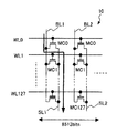
この実施例のフラッシュメモリのメモリアレイは、図3に示されているように、128個のメモリセルMC0〜MC127がビット線BL1,BL2……とソース線SL1,SL2……との間に並列に接続されたメモリ列が例えば8512個ワード線方向に並んで配設されている。本明細書ではこれをメモリブロックと称する。横方向つまり同一行のメモリセルはそれぞれ共通のワード線WL0,WL1,……WL127に接続されている。本明細書では、同一のワード線に接続されたメモリセル群をセクタと称する。本実施例のフラッシュメモリは、このセクタを単位として書込みと消去を行なうように構成されている。
【0026】
次に、上記実施例のフラッシュメモリをメモリカードに使用した場合の構成例を、図4を用いて説明する。
【0027】
図4に示されているように、メモリカードはフラッシュメモリ100と該フラッシュメモリ100にコマンドやアドレスを供給するマイクロプロセッサなどからなるコントローラLSI200とがセラミックなどのパッケージ300に封止されて構成される。
【0028】
パッケージ300には、電源電圧VCCおよびVSSが印加される電源端子T1,Tnや外部装置と接続される外部端子T2……が設けられ、電源端子T1,Tnにはボンディングワイヤやプリント配線基板に形成された配線等を介してコントローラLSI200とフラッシュメモリ100の電源端子が接続され、外部端子T2……にはコントローラLSI200の対応する入出力端子が接続されている。フラッシュメモリ100の制御ピンやI/OピンとコントローラLSI200の対応する端子との間もプリント配線基板に形成された配線等を介して接続されており、リセット信号/RESはコントローラLSI200からフラッシュメモリ100へ入力される。
【0029】
この実施例のメモリカードにおいては、フラッシュメモリ100およびコントローラLSI200とともに数10μF程度の電源コンデンサ400がパッケージ300に内蔵されている。この電源コンデンサ400は電源端子VCCとVSSとの間に接続されて、外部からの電源の供給が遮断されてもしばらくの間、フラッシュメモリ100に電源を供給できるように構成されている。
【0030】
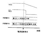
次に、本実施例のフラッシュメモリにおける消去および書込み動作の手順と、消去または書込み動作中に電源が遮断された場合の処理の手順の一例を、図5のタイミングチャートと図6および図7のフローチャートを用いて説明する。
【0031】
制御論理部16は、コントローラから消去を指示する第1コマンド(1stCMD)およびそれに付随する上位セクタアドレスSA1と下位セクタアドレスSA2を受信すると、内部電源回路23に対する起動信号や電圧変換回路18に対する電圧の指定信号などを生成して消去の準備を行なう(ステップS1〜S3)。それから、コントローラより開始を指示する第2コマンド(2ndCMD)を受信するとメモリセルに所定の電圧を印加して消去を開始する(ステップS4,S5)。その後、消去ベリファイを行なってしきい値電圧が充分に下がっていなければ再度消去電圧を印加する(ステップS6)。
【0032】
入力アドレスで指示されたすべてのメモリセルのしきい値電圧が所定の電圧以下に下がると、ステップS7へ移行してデプリート状態すなわちしきい値電圧が0V以下のメモリセルがあるか否かの判定が行なわれる。ここで、デプリート状態のメモリセルがなければ消去動作を終了し、デプリート状態のメモリセルがあればステップS8へ移行してしきい値電圧が低すぎるメモリセルに対してしきい値電圧を少し上げるためのバイアス電圧を印加する。
【0033】
その後、ステップS9でベリファイを行なってデプリート状態のメモリセルがなくなったか判定し、デプリチャージート状態のメモリセルなくなるまでバイアス電圧の印加を繰り返す。デプリート不良ビットがなくなるとステップS10で、メモリセルがディスターブ状態すなわちしきい値電圧が上がり過ぎた状態になっていないか判定する。そして、しきい値電圧が上がりすぎたものがあればステップS5へ戻ってしきい値電圧を下げる方向の電圧を印加する。すべてのメモリセルのしきい値電圧が所定の範囲に入ったことを確認すると消去動作を終了する。
【0034】
本実施例のフラッシュメモリは、上記ステップS1〜S4の第1コマンド受信から第2コマンド受信までの間に電源遮断▲1▼が発生してコントローラからリセット信号/RESが入力されると、直ちに消去動作を終了する。一方、ステップS5,S6の消去のためのバイアス電圧の印加とベリファイを行なっている間に電源遮断▲2▼が発生してコントローラからリセット信号/RESが入力されると、消去対象のメモリセルのしきい値電圧を最も高いデータ“01”に対応したしきい値電圧まで上げる書込み電圧を印加する書戻し処理を行なう。
【0035】
また、ステップS7〜S9のデプリートチェックと状態のメモリセルの書戻し処理を行なっている間に電源遮断▲3▼が発生してコントローラからリセット信号/RESが入力されると、動作を中断してデプリート状態のメモリセルがないかチェックしてなければ消去動作を終了し、デプリート状態のメモリセルがあれば該メモリセルに対してデータ“01”に対応したしきい値電圧まで上げる書戻し処理を行なう。なお、デプリート状態のメモリセルがないときは破線で示すようにステップS10へ移行するようにしてもよい。ステップS10移行の処理は比較的短時間に終了するからである。
【0036】
さらに、ステップS10のディスターブ判定を行なっている時に電源遮断▲4▼が発生してコントローラからリセット信号/RESが入力された場合には、直ちに動作を終了するように構成されている。
【0037】
電源遮断後に行なわれる上記書戻し処理は電源コンデンサ400に蓄積されている電荷がなくなる前に終了するように構成されている。言い換えると、電源遮断後に上記書戻し処理を実行できる程度に電源コンデンサ400の容量値が設定されている。
【0038】
以上、消去動作について説明したが、書込み動作も図6のフローチャートとほぼ同様である。書込み動作が消去動作と異なる点は、ステップS1で書込みコマンドを受信する点と、ステップS9の後で書込みデータに応じた所望のレベルまでしきい値電圧を上げるためのバイアス電圧印加とベリファイ動作を行なう点にある。
【0039】
ところで、図6のフローチャートは、電源遮断が発生してコントローラからリセット信号/RESが入力されたときに、フラッシュメモリ内部がどの状態にあるのか制御論理部16が分かっていることを前提にしたものである。
【0040】
図7には、内部がどの状態にあるのか制御論理部16が容易に判断できるようにした実施例が示されている。この実施例においては、第1コマンド受信後に行なわれる準備動作(初期設定S11)が終了した時点で動作チェックフラグを立てる(ステップS12)とともに、書込みまたは消去のためのバイアス電圧を印加(ステップS13)して最後のベリファイ動作(ステップS14)が終了した時点で動作チェックフラグを下げる処理(ステップS15)が設けられている。
【0041】
このように、動作チェックフラグを上げたり下げたりする処理を設けておけば、電源遮断が発生してコントローラからリセット信号/RESが入力されたときに、フラッシュメモリ内部がどの状態にあるのか容易に知ることができるため、その状態に応じた処理が可能になる。具体的には、動作チェックフラグが立つ前や動作チェックフラグが下がった後で電源遮断が発生してコントローラからリセット信号/RESが入力された場合には直ちに書込み又は消去動作を終了し、動作チェックフラグが立っている間に電源遮断が発生してコントローラからリセット信号/RESが入力された場合には、書込み又は消去動作を中断(ステップS16)し、しきい値電圧を高くする書戻し処理(ステップS17)を実行して終了する。
【0042】
なお、図7では図6の一部の処理の手順が簡略化して示されている。具体的には、図7のステップS11は図6のステップS1〜S4の処理に相当し、ステップS13はステップS5,S8に、またステップS14はステップS6,S7,S9に相当する。上記動作チェックフラグは、例えばステータスレジスタSTRの空きビットを利用して設定することができる。また、上記動作チェックフラグは、不揮発性記憶素子を利用して電源が完全に遮断した後も状態を保持するように構成することができる。さらに、上記動作チェックフラグとは別に、以下に述ベるように書込みまたは消去動作中に電源遮断が発生したか否かを電源遮断後も記憶する電源遮断フラグを設けるようにしてもよい。
【0043】
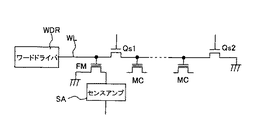
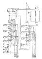
次に、上記不揮発性メモリの電源遮断フラグの構成例を、図8〜図11を用いて説明する。このうち、図8はワード線毎に電源遮断フラグを設けて電源遮断時に書込み、消去中であったセクタを識別できるようにしたものである。図8において、MCは不揮発性のメモリセル、WLはワード線、WDRは図1のアドレスデコーダ11内に設けられ対応するワード線を選択レベルに駆動するワードドライバである。図8に示されているように、この実施例では、ワード線WLにコントロールゲート端子が接続された不揮発性記憶素子からなるフラグメモリFMと、該フラグメモリFMのドレイン端子に接続されたセンスアンプSAとが設けられているとともに、ワード線WL上にはスイッチMOSFET Qs1,Qs2が設けられている。
【0044】
上記フラグメモリFMは、例えば初期設定でしきい値電圧が低い消去状態に設定しておいて、電源遮断時にセンスアンプSAに“1”をセットし、ワード線WLに高電圧を印加することによりしきい値電圧を高くすることでフラグがセットされた状態にさせることができる。また、このフラグメモリFMの書込みの際にはスイッチMOSFET Qs1をオフ状態、またQs2をオン状態にしてメモリアレイ内のメモリセルMCに影響を与えないでフラグの設定を行なうことができる。
【0045】
上記フラグメモリFMの読出しはメモリアレイを構成する記憶素子と同様にプリチャージ方式で行なうようにすることができる。ただし、メモリアレイを構成する記憶素子はしきい値電圧が4段階に設定され2ビットの情報を記憶するため、読出しはワード線に3段階の読出しレベルを設定して行なわれるが、フラグメモリFMの読出しは、ワード線に1つの読出しレベルを設定して、電流が流れるか否かを判定する簡易な判定方式とすることができる。
【0046】
この実施例は、フラグの数は多くなるが電源遮断時に書込みまたは消去中のセクタの判定が容易になるという利点がある。フラグの立ち下げすなわち消去はメモリアレイ内のメモリセルの消去の際にブロック単位で同時に行なうように構成することができる。
【0047】
図9は、アドレスのデコード処理が階層的なデコード方式になっている場合にメモリアレイの各ブロックに対応した電源遮断フラグBFMと、複数のブロックの同一ワード線に対応した共通の電源遮断フラグCFMとを設けて、電源遮断時に書込み、消去中であったセクタを識別できるようにしたものである。図9において、BLKはビット線およびソース線を共通にする並列形態のメモリセル列がワード線方向に所定数(例えば8512個)配列されてなるメモリブロック、WLはワード線、WDRはワード線を選択レベルに駆動するワードドライバ、W−DECはブロック内の1本のワード線を選択するワードデコーダ、B−DECは書込みまたは消去対象となるメモリセルを含むブロックを選択するブロックデコーダである。図9には示されていないが、電源遮断フラグBFMとCFMのドレイン端子にはセンスアンプが接続され、書込みと読出しが可能にされる。
【0048】
この実施例では、電源遮断フラグBFMとCFMを参照することにより、電源遮断時に書込みまたは消去中のセクタを識別することができるとともに、図8の実施例よりもフラグメモリの数が少なくて済むという利点がある。
【0049】
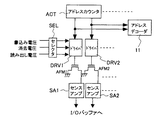
図10は、電源遮断時に書込み、消去中であったセクタのアドレスを保持するフラグメモリAFMを設けたものである。図10において、ACTは図1の制御論理部16内に設けられているアドレスカウンタ、11はアドレスをデコードしてメモリアレイ内のワード線を選択するアドレスデコーダである。この実施例では、アドレスを記憶するためのフラグメモリAFM1,AFM2……と、該フラグメモリのゲート端子に印加する電圧を生成するドライバDRV1,DRV2……と、各フラグメモリのドレイン端子に接続されセンスアンプSA1,SA2……と、上記ドライバに動作モードに応じて書込み電圧または消去電圧、読出し電圧のいずれかを供給するセレクタSELとが設けられている。フラグメモリAFMとドライバDRVとセンスアンプSAは、アドレスのビット数分だけ設けられる。
【0050】
この実施例は、図8や図9の実施例に比べてフラグメモリの数を大幅に少なくできるという利点がある。なお、フラグメモリAFMは書込み動作または消去動作が発生するたびに設定を行なってもよいが、電源遮断が発生した時にだけ設定を行なうようにすることもできる。
【0051】
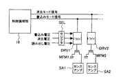
図11は、書込み、消去中に電源遮断が発生した場合に電源遮断時の動作モードが書込みモードであったのか消去モードであったのかを記憶するモードフラグメモリMFM1,MFM2を設けたものである。この実施例では、制御論理部16から動作モードを示すモード信号が出力されるとともに、該モード信号を入力としフラグメモリMFM1,MFM2のゲート端子に印加する電圧を生成するドライバDRV1,DRV2と、各フラグメモリMFM1,MFM2のドレイン端子に接続されセンスアンプSA1,SA2と、上記ドライバドライバDRV1,DRV2に動作モードに応じて書込み電圧または消去電圧、読出し電圧のいずれかを供給するセレクタSELとが設けられている。
【0052】
この実施例は、図10の実施例よりもさらにフラグメモリの数を少なくできるという利点がある。なお、フラグメモリMFM1,MFM2は書込み動作または消去動作が発生するたびに設定を行なってもよいが、電源遮断が発生した時に行なうようにすることもできる。また、図11の実施例は、図8〜図10の実施例と組み合わせて適用することで、より優れた利点が得られる。
【0053】
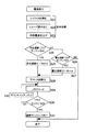
次に、図8または図9の実施例と図11の実施例を組み合わせた場合におけるフラグの読出し方式の一例を、図12のフローチャートを用いて説明する。
【0054】
電源が投入されると、制御論理部16はチップ内部の各種レジスタの初期化を行なう(ステップS21)。続いてトリミングや電源設定等のためのヒューズの状態の読出しを行なってから、内部電源回路23に起動信号を送って内部電源を立ち上げる(ステップS22,S23)。ここまでは、従来のフラッシュメモリと同様の動作である。
【0055】
この実施例では、内部電源立上げ後に制御論理部16がフラグサーチ処理を開始して、先ずステップS24で消去遮断フラグMFM2が立っているか判定し、立っていないときはステップS26へ移行して書込み遮断フラグMFM1が立っているか判定し、いずれのフラグも立っていないときはそのままフラグサーチ処理を終了する。消去遮断フラグMFM2または書込み遮断フラグMFM1が立っているときは、ステップS25,S27でそれぞれステータスレジスタSTRに消去中の電源遮断または書込み中の電源遮断があったことを示すビットをセットする。
【0056】
それから、アドレスカウンタをオールゼロに初期化して先頭アドレスをアドレスデコーダに供給してフラグメモリFMの読出しを行なう(ステップS28,S29)。次に、読み出したフラグが立っているか判定(ステップS30)し、立っているときはそのときのアドレスカウンタの値を遮断アドレスとしてアドレスレジスタADRにセットして終了する(ステップS31)。一方、ステップS30でフラグが立っていないと判定した時はステップS32でアドレスカウンタをインクリメント(+1)してステップS28へ戻り、次のアドレス(セクタ)のフラグメモリの読み出しを行ない、立っているフラグが見つかるまで上記動作を繰り返す。
【0057】
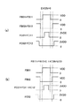
図13および図14には、上記フローチャートに従ってアドレスレジスタADRにセットされた遮断アドレスを、外部のコントローラが読み出せるようにしたフラッシュメモリの読出しタイミングの例を示す。
【0058】
図13は、コントローラがフラッシュメモリに対して所定のコマンドを送って読み出すように構成した場合のタイミングである。
【0059】
フラッシュメモリは、電源が立ち上がると初期設定およびフラグサーチを行ない、終了するとレディ/ビジー信号R/Bをレディ状態を示すハイレベルに変化させる(タイミングt1)。コントローラはこれを検知するとチップイネーブル信号/CE、出力イネーブル信号/OEをロウレベルに変化させる(タイミングt2,t3)。すると、入出力ピンI/O0〜7からステータスレジスタSTRの内容が出力される(タイミングt4)。その後、コントローラがコマンドイネーブル信号/CMDをロウレベルに変化させるとともに、入出力ピンI/O0〜7から遮断アドレスリードコマンドを入力する(タイミングt5)。そして、リードイネーブル信号/REをロウレベルとハイレベルに交互に変化させると、アドレスレジスタADRに保持されている例えば16ビットの遮断アドレスが8ビットずつ入出力ピンI/O0〜7から出力される(タイミングt6,t7)。
【0060】
図14は、コントローラがフラッシュメモリに設けられている所定の外部端子に制御信号を入力することにより、アドレスレジスタADRに保持されている遮断アドレスを読み出すように構成した場合のタイミングである。
【0061】
フラッシュメモリは、電源が立ち上がると初期設定およびフラグサーチを行ない、終了するとレディ/ビジー信号R/Bをレディ状態を示すハイレベルに変化させる(タイミングt11)。コントローラは、電源の立ち上がりと同時にフラッシュメモリの所定の外部端子(オートリード)をハイレベルに固定するとともに、レディ/ビジー信号R/Bのハイレベルの変化を検知してチップイネーブル信号/CEに変化させる(タイミングt12)。それから、リードイネーブル信号/REをロウレベルとハイレベルに交互に変化させると、ステータスレジスタSTRの内容とアドレスレジスタADRに保持されている遮断アドレスが順次入出力ピンI/O0〜7から出力される(タイミングt13,t14,t15)。これにより、パワーオン時における遮断アドレスのオートリードが実行される。
【0062】
さらに、本実施例のフラッシュメモリは、外部から供給される電源電圧のレベルに応じて内部電源回路23が動作するように構成されている。
【0063】
図15は、内部電源回路23を構成するチャージポンプの一実施例を示す。この実施例のチャージポンプは、電源電圧端子VCCとクロック入力端子CKinとの間に直列に接続されたスイッチSW1および容量CB1と、スイッチSW1と容量CB1との接続ノードN1と出力端子OUTとの間に直列に接続されたn−1個のスイッチSW2〜SWnと、スイッチSW2〜SWnの各接続ノードN2〜Nnに前記容量CB1と並列に接続された容量CB2〜CBn-1とを備え、奇数番目のノードに接続された容量CB1,CB3,……CBn-2の他端にはクロックφ1またはこれと同相のクロックφ2,φ3が印加され、偶数番目のノードに接続された容量CB2,CB4,……CBn-1の他端にはクロックφ1,φ2,φ3と逆相のクロック/φ1,/φ2,/φ3が印加されている。
【0064】
また、奇数番目のスイッチSW1,SW3,……SWn-1はクロックφ1によりオン、オフされ、偶数番目のスイッチSW2,SW4,……SWnは逆相のクロック/φ1によりオン、オフされる。これにより、スイッチSW1により容量CB1にチャージされた電荷が容量CB2〜CBn-1を左から右ヘ向って順次転送されて行き昇圧動作が行なわれる。かかる構成のチャージポンプは従来公知のチャージポンプとほぼ同様な構成である。
【0065】
この実施例のチャージポンプは、上記構成に加え、容量CBn-2とスイッチSWn-1の接続ノードNn-1と出力端子OUTとの間および容量CBn-4とスイッチSWn-3の接続ノードNn-3と出力端子OUTとの間にそれぞれ段数切替え用のスイッチSW11,SW12が設けられている。これらのスイッチSW11,SW12はそれぞれ制御論理部16から供給される切替信号EXC1,EXC2によりオン状態またはオフ状態にされる。
【0066】
スイッチSW11とSW12が共にオフ状態にされるとSW11とSW12がない場合と同じように動作することで図15の回路は(n−1)段のチャージポンプとして動作し、スイッチSW11がオン、SW12がオフ状態にされるとSW11を介してノードNn-1の電荷が出力端子OUTへ供給されることで図15の回路は(n−3)段のチャージポンプとして動作し、スイッチSW11がオフ、SW12がオン状態にされるとSW12を介してノードNn-3の電荷が出力端子OUTへ供給されることで図15の回路は(n−5)段のチャージポンプとして動作する。つまり、図15のチャージポンプは昇圧段数が変更可能に構成されている。
【0067】
図16(a)には図15の回路を(n−1)段のチャージポンプとして動作させる場合に印加されるクロックφ1〜φ3,/φ1〜/φ3のタイミングを示す。図示されているように、φ1,φ2,φ3は互いに同一のタイミング、/φ1,/φ2,/φ3も互い同一のタイミングでよい。φ1と/φ1は、電荷が逆方向に転送されるのを防止するため、互いにハイレベルの期間が重ならないようにされた逆相のクロックとされる。図16(b)には図15の回路を(n−3)段のチャージポンプとして動作させる場合に印加されるクロックφ1,φ2,/φ1,/φ2のタイミングを示す。図示されているように、φ1,φ2は互いに同一のタイミング、/φ1,/φ2も互い同一のタイミングとされる。φ3と/φ3はロウレベルに固定される。図16(c)には図15の回路を(n−5)段のチャージポンプとして動作させる場合に印加されるクロックφ1,/φ1のタイミングを示す。φ2とφ2およびφ3と/φ3はロウレベルに固定される。
【0068】
ところで、図15のチャージポンプは、スイッチSW11をオンさせる(n−3)段動作時に、電荷転送用のスイッチSWn-1はクロックφ3により、またスイッチSWnはクロック/φ3によりオフ状態にさせておいても昇圧動作をする。これに対し、図示されているように、スイッチSW11がオンの時にもスイッチSWn-1をクロックφ1により、またスイッチSWnをクロック/φ1によりオン、オフさせることにより、昇圧用容量CBn-2,CBn-1を平滑容量として利用できるようになる。つまり、平滑容量CDの見かけ上の容量値を増加させることができる。スイッチSW12をオンさせる(n−5)段動作時についても同様であり、昇圧用容量CBn-4,CBn-3,CBn-2,CBn-1を平滑容量として利用できるようになる。
【0069】
本実施例のフラッシュメモリは、電源電圧VCCのレベルに応じて上記チャージポンプの段数を変更するような制御を行なう。具体的には、電源電圧VCCのレベルが高いときは段数の少ない(n−5)段で動作させ、電源電圧VCCのレベルが少し下がったときは段数を減らして(n−3)段で動作させ、電源電圧VCCのレベルがさらに下がったときは(n−1)段で動作させるように構成されている。これにより、電源電圧VCCが高い時も低い時も所望の所望の昇圧電圧が得られるとともに、出力のリップルを小さくすることができる。すなわち、電源電圧VCCが高い時は段数が少ないため段数が多い場合よりも出力のリップルが大きくなるが、上記実施例のように段数が少ない時は平滑容量CDの容量値が大きくされることによりリップルを抑えることができる。
【0070】
本発明者らが開発している128MBのフラッシュメモリにおいて見積もりを行なったところ、容量CBn-4,CBn-3,CBn-2,CBn-1を平滑容量として利用しないでその分平滑容量CDの容量値を大きくしようとすると、平滑容量CDの占有面積は0.18mm2、チップサイズに対する比率で約0.4%、内部電源回路23の占有面積に対する比率では約5%も大きくする必要があることが分かった。従って、本実施例を適用することにより、チップサイズを約0.4%小さくすることができる。
【0071】
図17は内部電源回路23を構成するチャージポンプの他の実施例を示す。この実施例のチャージポンプは、スイッチSW11のオン、オフによりチャージポンプを4段と8段の2段階に切替え可能に構成されている。また、電荷転送用のスイッチ(図15のSW2〜SWn)としてMOSFET QT1〜QT8を用いているとともに、このスイッチMOSFET QT1〜QT8を充分にオンさせて転送効率を高めるためにブースト用の容量CGが設けられている。QGはこのブースト用容量CGをチャージするためのスイッチMOSFETである。
【0072】
さらに、特に制限されるものでないが、この実施例では、各ノードN0〜N7と電源電圧端子VCCとの間にはダイオードとして動作するMOSFET QBが設けられており、昇圧開始時に各ノードに電荷を直接注入して到達時間を短縮できるように構成されている。なお、LSFは段数切替えスイッチSW11をオン、オフ制御する切替え信号EXCを昇圧電圧VPPに近いレベルまでシフトするレベルシフト回路である。図17の実施例では、段数切替えスイッチSW11にNチャネルMOSFETを用いているが、PチャネルMOSFETを用いるようにしてもよい。
【0073】
図18(a)には図17の回路を8段のチャージポンプとして動作させる場合に印加されるクロックのタイミングが、また図18(b)には図17の回路を4段のチャージポンプとして動作させる場合に印加されるクロックのタイミングが示されている。図において、FB01,FB02,FB11,FB12は昇圧動作用のクロック、FC1,FC2はブースト用容量CGをたたいて電荷転送用MOSFET QT1〜QT8のゲート電圧を押し上げるクロックである。4段のチャージポンプとして動作させる場合、スイッチSW11はオン状態とされ、クロックFB11,FB12はロウレベル(0V)に固定される。この実施例においても、4段のチャージポンプとして動作するときには、後段の昇圧用容量CBは平滑容量として利用されるように電荷転送用MOSFET QT5〜QT8が制御される。
【0074】
図19は内部電源回路23を構成するチャージポンプのさらに他の実施例を示す。この実施例のチャージポンプは、図17のチャージポンプでは前段と後段でブースト用のクロックを共通に用いていたものを、別々のブースト用クロックFC01,FC02;FC11,FC12で動作させるようにしたものである。図20(a)には図19の回路を8段のチャージポンプとして動作させる場合に印加されるクロックのタイミングが、また図20(b)には図18の回路を4段のチャージポンプとして動作させる場合に印加されるクロックのタイミングが示されている。図20のようなクロックによってチャージポンプを動作させることにより、図18のチャージポンプよりも4段動作時における平滑容量CDの効率をさらに向上させることができる。
【0075】
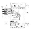
次に、本発明の変形例を説明する。この変形例は、図21に示すように、ヒューズ素子を含む回路などからなり使用する電源電圧に応じて電源を設定する電源設定回路24を設けるとともに、電源電圧検出回路19として電源電圧VCCのレベルを3段階以上に区別して検出し、電源設定状態に応じて電源遮断を検出することができる電源遮断検出回路25を設けたものである。前記段数切替え可能なチャージポンプは、上記電源設定回路24の電源設定に応じて段数が設定されるように構成することもできる。
【0076】
電源遮断検出回路25は、上記電源電圧検出回路19からの検出信号DTC1,DTC2,DTC3……を電源設定回路24の電源設定状態に応じて選択的に通過させるゲートG1〜G5……と、上記検出信号DTC1,DTC2,DTC3……のいずれかを起動信号および停止信号として動作クロックCLKを計数するカウンタCNTと、該カウンタが計時する時間を設定するタイマ設定レジスタTMRと、カウンタCNTの計数値とタイマ設定レジスタTMRの設定値とを比較するコンパレータCMPとから構成されている。タイマ設定レジスタTMRの設定値は電源設定回路24の電源設定状態に応じて異なる値とされる。
【0077】
電源設定回路24の電源設定状態が最も高い状態1に設定されていると、ゲートG1とG2が開かれて電源電圧検出回路19からの検出信号DTC1を起動信号としてまた検出信号DTC2を停止信号としてカウンタCNTに供給する。電源設定回路24の電源設定状態が2番目に高い状態2に設定されていると、ゲートG3とG5が開かれて電源電圧検出回路19からの検出信号DTC2を起動信号としてまた検出信号DTC3を停止信号としてカウンタCNTに供給する。
【0078】
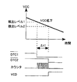
図22には、電源設定回路24において電源設定状態1が設定されている場合の動作波形が示されている。電源電圧VCCが低下して検出レベル1に到達すると検出信号DTC1がハイレベルからロウレベルに変化し、これに応じてカウンタCNTがクロックの計数を開始する。そして、電源電圧VCCがさらに低下して検出レベル2に到達すると検出信号DTC2がハイレベルからロウレベルに変化し、これに応じてカウンタCNTが計数動作を停止する。このときカウンタCNTに計数された値が設定値よりも大きくなるとコンパレータCMPの出力信号である電源遮断検出信号VCDがロウレベルからハイレベルに変化される。これによって制御論理部16は電源遮断が発生したことを知ることができる。
【0079】
以上本発明者によってなされた発明を実施例に基づき具体的に説明したが、本発明は上記実施例に限定されるものではなく、その要旨を逸脱しない範囲で種々変更可能であることはいうまでもない。例えば、実施例においては、1つの記憶素子(メモリセル)に2ビットのデータを記憶可能な4値のフラッシュメモリについて説明したが、本発明は1つの記憶素子に1ビットのデータを記憶する2値のフラッシュメモリや3ビット以上のデータを記憶する多値のフラッシュメモリに対しても適用することができる。
【0080】
また、実施例においてはメモリセルのしきい値電圧が低い状態を消去状態と称し、しきい値電圧が高い状態を書込み状態と称しているが、メモリセルのしきい値電圧が高い状態を消去状態に対応させ、しきい値電圧が低い状態を書込み状態に対応させるようにしたフラッシュメモリに対しても本発明を適用することができる。
【0081】
さらに、前記実施例においては、複数の記憶素子がビット線とソース線との間に並列に接続されたいわゆるAND型もしくはNOR型のフラッシュメモリについて説明したが、本発明は記憶素子が直列に接続されたいわゆるNAND型のフラッシュメモリや、MONOS構造のメモリセルを持つ不揮発性メモリ等に対しても適用することができる。NAND型等のフラッシュメモリでは、デプリート状態のメモリセルが存在することによりブロック内のデータがすべて不正確になるということはないが、電源遮断でデプリート状態のまま残ったメモリセルがあっても本発明を適用することで修復が可能になる。
【0082】
即ち、図8から図14において説明した技術を適用することにより、書込み又は消去途中に電源遮断が生じ、該メモリセルに格納されているデータは不正確であり使用することができない事を知ることができる。これにより該メモリセルに格納されているデータを誤って使用して、望まない結果が生じることを防ぐことができる。またAND型若しくはNOR型のフラッシュメモリではデプリート状態のメモリセルが存在しているとシステム全体として動作できなくなる虞があるため、前記実施例では書込み又は消去途中に電源遮断が生じたか否か確認をする動作を説明したが、NAND型のフラッシュメモリ等であればデプリート状態のメモリセルが存在していてもシステム全体として動作することは可能であるため、読み出しや書込みを行なう際に、確認の動作を行なうようにしても良い。
【0083】
以上の説明では主として本発明者によってなされた発明をその背景となった利用分野であるフラッシュメモリに適用した場合について説明したが、この発明はそれに限定されるものでなく、本発明は、電圧を印加してしきい値電圧を変化させて情報の記憶を行なう不揮発性記憶素子を有する半導体メモリに広く利用することができる。
【0084】
【発明の効果】
本願において開示される発明のうち代表的なものによって得られる効果を簡単に説明すれば下記のとおりである。
【0085】
すなわち、本発明に従うと、書込みまたは消去の動作が完全に終了する前に電源遮断が発生してデプリート状態のメモリセルが発生しても、その後の書戻し処理でメモリセルのしきい値電圧が高くされるため、ブロック全体のデータが正しく読めなくなる事態に至るのを回避できるようになる。
【0086】
また、書込みまたは消去の途中で電源遮断が発生したことを外部へ知らせるフラグを設けたことにより、ホストCPUなどの外部装置が、電源遮断で破損したメモリ内のデータの修復を行なうことができるようになる。これによって、電源遮断でシステム領域のデータが破損しても修復を行なうことで、メモリの認識ができなくなったりシステムの正常動作が不能になるのを回避することができる。
【0087】
さらに、電源電圧のレベルに応じて内部電源(チャージポンプの段数)を切り替えるように構成したので、電源遮断により電源電圧が低下してもそれに応じて内部電源が動作して所望の電圧を発生することによって、書戻し処理を確実に実行することができるようになり、メモリの信頼性が向上するようになる。
【図面の簡単な説明】
【図1】本発明を適用して有効な不揮発性半導体記憶装置の一例としてのフラッシュメモリの実施例を示すブロック図である。
【図2】実施例のフラッシュメモリのメモリセルのしきい値電圧分布を示す説明図である。
【図3】実施例のフラッシュメモリのメモリアレイの構成例を示す回路説明図である。
【図4】実施例のフラッシュメモリを利用したメモリカードの一構成例を示すブロック図である。
【図5】実施例のフラッシュメモリにおける消去および書込み動作と、消去または書込み動作中に電源が遮断された場合の処理の動作タイミングの一例を示すタイミングチャートである。
【図6】実施例のフラッシュメモリにおける消去および書込み動作の手順と、消去または書込み動作中に電源が遮断された場合の処理の手順の一例を示すフローチャートである。
【図7】実施例のフラッシュメモリにおける消去および書込み動作の手順と、消去または書込み動作中に電源が遮断された場合の処理の手順の他の例を示すフローチャートである。
【図8】実施例のフラッシュメモリにおける電源遮断フラグの構成例を示す説明図である。
【図9】実施例のフラッシュメモリにおける電源遮断フラグの他の構成例を示す説明図である。
【図10】実施例のフラッシュメモリにおける電源遮断時のアドレスを保持するフラグの構成例を示す説明図である。
【図11】実施例のフラッシュメモリにおける電源遮断時の動作状態を保持するフラグの構成例を示す説明図である。
【図12】実施例のフラッシュメモリにおける電源投入時におけるフラグサーチ処理の手順の一例を示すフローチャートである。
【図13】実施例のフラッシュメモリにおける電源投入時における遮断アドレスの外部読出しのタイミングの一例を示すタイミングチャートである。
【図14】実施例のフラッシュメモリにおける電源投入時における遮断アドレスの外部読出しのタイミングの他の例を示すタイミングチャートである。
【図15】内部電源回路を構成するチャージポンプの一実施例を示す回路図である。
【図16】(a)は図15の回路を(n−1)段のチャージポンプとして動作させる場合に印加されるクロックのタイミング、(b)は図15の回路を(n−3)段のチャージポンプとして動作させる場合に印加されるクロックのタイミング、(c)は図15の回路を(n−5)段のチャージポンプとして動作させる場合に印加されるクロックのタイミングを示すタイミングチャートである。
【図17】内部電源回路を構成するチャージポンプの他の実施例を示す回路図である。
【図18】(a)は図17の回路を8段のチャージポンプとして動作させる場合に印加されるクロックのタイミング、(b)は図17の回路を4段のチャージポンプとして動作させる場合に印加されるクロックのタイミングを示すタイミングチャートである。
【図19】図17のチャージポンプの変形例を示す回路図である。
【図20】(a)は図19の回路を8段のチャージポンプとして動作させる場合に印加されるクロックのタイミング、(b)は図19の回路を4段のチャージポンプとして動作させる場合に印加されるクロックのタイミングを示すタイミングチャートである。
【図21】本発明の変形例としての電源遮断検出回路を備えたフラッシュメモリの電源遮断検出部の構成例を示すブロック図である。
【図22】図21の電源遮断検出部の動作波形例を示す波形図である。
【符号の説明】
10 メモリアレイ
11 アドレスデコーダ
16 制御論理部
19 電源検出回路
23 内部電源回路
25 電源遮断検出回路
MC メモリセル
WL ワード線
BL ビット線
SL ソース線
STR ステータスレジスタ
ADR アドレスレジスタ
WDR ワードドライバ
CFM フラグメモリ[0001]
BACKGROUND OF THE INVENTION
BACKGROUND OF THE
[0002]
[Prior art]
Flash memory uses a non-volatile memory element consisting of a double-gate MOSFET having a control gate and a floating gate as a memory cell, and changes the threshold voltage of the MOSFET by changing the amount of charge stored in the floating gate. Information is stored.
[0003]
In such a flash memory, the threshold voltage may be changed to a low state during a write / erase operation to the memory cell. In this case, the threshold voltage varies depending on the memory cell characteristic variation, and the threshold voltage may drop to 0 V or less (hereinafter referred to as a depleted state). Normally, the threshold voltage of the memory cell whose threshold voltage has decreased too much is set to fall within a predetermined range by an operation called write-up or write-back.
[0004]
[Problems to be solved by the invention]
However, in a flash memory used for a memory card or the like, the power supply may be interrupted during a write or erase operation when a power failure occurs or the user pulls the card out of the slot. Therefore, some memory cells in the memory array may remain in a depleted state due to power shutdown. When such a depleted memory cell is generated, a so-called AND-type or NOR-type flash memory in which a plurality of memory cells MC are connected in parallel between a bit line BL and a source line SL as shown in FIG. In this case, a current flows through a memory cell that is not selected and is in a depleted state, and a depletion failure occurs in which stored data in the selected memory cell cannot be read accurately.
[0005]
If the block including the memory cell that has caused the depletion failure is used as a system area for storing data important for the system, such as table data and format information for managing the position of the file on the memory, There is a risk that recognition may be disabled or normal operation of the system may be disabled.
[0006]
An object of the present invention is to prevent a memory cell in a depleted state from being generated even in the case where a power interruption occurs during a write or erase operation in an electrically writable / erasable nonvolatile semiconductor memory device such as a flash memory. Is to make it.
[0007]
Another object of the present invention is that in a non-volatile semiconductor memory device such as a flash memory that can be electrically written and erased, if the power supply is interrupted during the write or erase operation, the power supply is interrupted. The purpose is to enable an external device to recognize.
[0008]
Still another object of the present invention is to provide an electrically writable / erasable nonvolatile semiconductor memory device such as a flash memory so that the memory cannot be recognized or the system operates normally due to power interruption during the writing or erasing operation. It is to be able to avoid being disabled.
[0009]
The above and other objects and novel features of the present invention will be apparent from the description of this specification and the accompanying drawings.
[0010]
[Means for Solving the Problems]
The following is a brief description of an outline of typical inventions disclosed in the present application.
[0011]
That is, according to the first invention of this application, in a nonvolatile semiconductor memory device such as a flash memory, when a power interruption occurs during a write or erase operation, the current operation is interrupted and the threshold voltage is set. It is configured to perform a write-back process that changes the direction to be increased.
[0012]
According to the above-described means, even if a power-off occurs before a write or erase operation is completely completed and a memory cell in a depleted state is generated, the threshold voltage of the memory cell is changed in the subsequent write-back process. Therefore, it is possible to avoid a situation where the data of the entire block cannot be read correctly.
[0013]
According to another invention of the present application, in a nonvolatile semiconductor memory device such as a flash memory, a flag is provided to notify the outside of the occurrence of power interruption when the power interruption occurs at least during a write or erase operation. I did it. Desirably, a function of outputting an address accessed at the time of power-off is provided. As a result, the external device such as the host CPU can restore the data in the memory that is damaged by the power shutdown.
[0014]
According to still another aspect of the present invention, in a nonvolatile semiconductor memory device such as a flash memory, when a power interruption occurs during a write or erase operation, the current operation is interrupted to increase the threshold voltage. In addition to performing a write-back process that changes the direction, the internal power supply circuit (number of stages of the charge pump) can be switched according to the level of the power supply voltage so that the write-back process can be performed. As a result, even if the power supply voltage drops due to power shutoff, the internal power supply circuit generates an operating voltage accordingly, so that the write-back process can be executed reliably.
[0015]
DETAILED DESCRIPTION OF THE INVENTION
Hereinafter, an embodiment of the present invention will be described with reference to the drawings.
[0016]
FIG. 1 shows a block diagram of an embodiment of a flash memory as an example of a nonvolatile semiconductor memory device effective by applying the present invention. The flash memory has a binary memory capable of storing 1-bit data in one memory cell, but the flash memory of this embodiment is configured as a quaternary memory capable of storing 2-bit data in one memory cell. It is formed on a single semiconductor chip such as single crystal silicon.
[0017]
In FIG. 1,
[0018]
Although not particularly limited, in this embodiment, the state with the highest threshold voltage corresponds to the data “01”, the state with the second highest threshold voltage is the data “00”, and the threshold value. The state with the third highest voltage corresponds to data “10”, and the state with the lowest threshold voltage corresponds to data “11”. In this specification, the state having the lowest threshold voltage is referred to as an erased state. That is, the operation for lowering the threshold voltage is called erasing, and the operation for raising the threshold voltage is called writing or writing-back. In the flash memory of this embodiment, when data in the
[0019]
In FIG. 1,
[0020]
[0021]
Further, the
[0022]
The flash memory of this embodiment is not particularly limited, but a power supply
[0023]
In the flash memory of this embodiment, the
[0024]
Further, the flash memory of this embodiment has a control pin C1 to which, for example, a chip selection signal / CE, a write control signal / WE, an output control signal / OE, a read control signal / RE, and the like input from an external controller are input. To Cn. Control signals input to these control pins are supplied to the
[0025]
In the memory array of the flash memory of this embodiment, as shown in FIG. 3, 128 memory cells MC0 to MC127 are arranged in parallel between bit lines BL1, BL2... And source lines SL1, SL2. For example, 8512 memory columns are arranged in the word line direction. In this specification, this is called a memory block. The memory cells in the horizontal direction, that is, in the same row are connected to common word lines WL0, WL1,. In this specification, a group of memory cells connected to the same word line is referred to as a sector. The flash memory of this embodiment is configured to perform writing and erasing in units of this sector.
[0026]
Next, a configuration example when the flash memory of the above embodiment is used for a memory card will be described with reference to FIG.
[0027]
As shown in FIG. 4, the memory card is configured by sealing a
[0028]
The
[0029]
In the memory card of this embodiment, the
[0030]
Next, an example of the procedure of erasing and writing operations in the flash memory of this embodiment and an example of the processing procedure when the power is shut off during the erasing or writing operation are shown in the timing chart of FIG. 5 and FIGS. This will be described with reference to a flowchart.
[0031]
When the
[0032]
When the threshold voltage of all the memory cells indicated by the input address falls below a predetermined voltage, the process proceeds to step S7 to determine whether there is a depleted state, that is, whether there is a memory cell whose threshold voltage is 0 V or less. Is done. If there is no memory cell in the depleted state, the erase operation is terminated. If there is a memory cell in the depleted state, the process proceeds to step S8 and the threshold voltage is slightly increased for the memory cell whose threshold voltage is too low. A bias voltage is applied.
[0033]
Thereafter, verify is performed in step S9 to determine whether or not there are no depleted memory cells, and the application of a bias voltage is repeated until there are no more depleted memory cells. When the depletion failure bit disappears, it is determined in step S10 whether the memory cell is in a disturbed state, that is, a state in which the threshold voltage is excessively increased. If there is a voltage whose threshold voltage has increased too much, the process returns to step S5 to apply a voltage in the direction of decreasing the threshold voltage. When it is confirmed that the threshold voltages of all the memory cells are within a predetermined range, the erase operation is terminated.
[0034]
The flash memory according to the present embodiment is immediately erased when the power cut-off (1) occurs between the first command reception and the second command reception in steps S1 to S4 and the reset signal / RES is input from the controller. End the operation. On the other hand, when the power shut-off (2) occurs and the reset signal / RES is input from the controller while the bias voltage is applied and verified in steps S5 and S6, the memory cell to be erased A write-back process is performed in which a write voltage is applied to raise the threshold voltage to the threshold voltage corresponding to the highest data “01”.
[0035]
In addition, when the power cut (3) occurs and the reset signal / RES is input from the controller while the depletion check in steps S7 to S9 and the write-back processing of the memory cell in the state are performed, the operation is interrupted. If it is not checked whether there is a memory cell in the depleted state, the erase operation is terminated. If there is a memory cell in the depleted state, a write-back process for raising the memory cell to the threshold voltage corresponding to the data “01” To do. When there is no memory cell in the depleted state, the process may move to step S10 as indicated by a broken line. This is because the process of step S10 is completed in a relatively short time.
[0036]
Further, when the power cut (4) occurs and the reset signal / RES is input from the controller during the disturb determination in step S10, the operation is immediately terminated.
[0037]
The write-back process performed after the power is shut off is configured to end before the electric charge accumulated in the
[0038]
The erase operation has been described above, but the write operation is almost the same as the flowchart of FIG. The write operation differs from the erase operation in that a write command is received in step S1, and a bias voltage application and verify operation for raising the threshold voltage to a desired level according to write data after step S9. There is a point to do.
[0039]
By the way, the flowchart of FIG. 6 is based on the premise that the
[0040]
FIG. 7 shows an embodiment in which the
[0041]
In this way, if a process for raising or lowering the operation check flag is provided, it is easy to determine the internal state of the flash memory when the power cut occurs and the reset signal / RES is input from the controller. Since it can be known, processing according to the state becomes possible. Specifically, when the power cut occurs before the operation check flag is set or after the operation check flag is lowered and the reset signal / RES is input from the controller, the write or erase operation is immediately terminated and the operation check is performed. When the power is cut off while the flag is set and the reset signal / RES is input from the controller, the write or erase operation is interrupted (step S16), and the write-back process for increasing the threshold voltage ( Step S17) is executed and the process ends.
[0042]
In FIG. 7, a part of the processing procedure of FIG. 6 is simplified. Specifically, step S11 in FIG. 7 corresponds to the processing in steps S1 to S4 in FIG. 6, step S13 corresponds to steps S5 and S8, and step S14 corresponds to steps S6, S7, and S9. The operation check flag can be set using, for example, an empty bit of the status register STR. In addition, the operation check flag can be configured to maintain the state even after the power supply is completely shut down using the nonvolatile memory element. In addition to the operation check flag, as described below, a power cut-off flag may be provided for storing whether or not a power cut has occurred during a write or erase operation even after the power is cut off.
[0043]
Next, a configuration example of the power cutoff flag of the nonvolatile memory will be described with reference to FIGS. Of these, FIG. 8 is provided with a power cut-off flag for each word line so that a sector which is being written or erased when the power is cut off can be identified. In FIG. 8, MC is a non-volatile memory cell, WL is a word line, and WDR is a word driver provided in the
[0044]
For example, the flag memory FM is set to an erase state in which the threshold voltage is low in the initial setting, and when the power is shut off, the sense amplifier SA is set to “1” and a high voltage is applied to the word line WL. By raising the threshold voltage, the flag can be set. When writing to the flag memory FM, the flag can be set without affecting the memory cells MC in the memory array by turning off the switch MOSFET Qs1 and turning on the Qs2.
[0045]
Reading of the flag memory FM can be performed by a precharge method in the same manner as the storage elements constituting the memory array. However, since the storage elements constituting the memory array have threshold voltages set to 4 levels and store 2-bit information, reading is performed by setting 3 levels of read levels on the word lines. This reading can be a simple determination method in which one read level is set for the word line to determine whether or not a current flows.
[0046]
This embodiment has the advantage that the number of flags increases, but it becomes easy to determine the sector being written or erased when the power is shut off. The flag can be lowered or erased simultaneously in units of blocks when erasing the memory cells in the memory array.
[0047]
FIG. 9 shows a power-off flag BFM corresponding to each block of the memory array and a common power-off flag CFM corresponding to the same word line of a plurality of blocks when the address decoding process is a hierarchical decoding method. Are provided so that the sector being written or erased when the power is shut off can be identified. In FIG. 9, BLK is a memory block in which a predetermined number (for example, 8512) of memory cell columns arranged in parallel with a bit line and a source line are arranged in the word line direction, WL is a word line, and WDR is a word line. A word driver for driving to a selection level, W-DEC is a word decoder for selecting one word line in the block, and B-DEC is a block decoder for selecting a block including a memory cell to be written or erased. Although not shown in FIG. 9, a sense amplifier is connected to the drain terminals of the power shutoff flags BFM and CFM to enable writing and reading.
[0048]
In this embodiment, by referring to the power shutdown flags BFM and CFM, it is possible to identify the sector that is being written or erased when the power is shut off, and the number of flag memories can be smaller than in the embodiment of FIG. There are advantages.
[0049]
FIG. 10 is provided with a flag memory AFM that holds the address of the sector that was being written or erased when the power was turned off. In FIG. 10, ACT is an address counter provided in the
[0050]
This embodiment has the advantage that the number of flag memories can be significantly reduced compared to the embodiments of FIGS. Note that the flag memory AFM may be set every time a write operation or an erase operation occurs, but may be set only when a power interruption occurs.
[0051]
FIG. 11 is provided with mode flag memories MFM1 and MFM2 for storing whether the operation mode at the time of power-off is the writing mode or the erasing mode when the power-off occurs during writing and erasing. . In this embodiment, a mode signal indicating an operation mode is output from the
[0052]
This embodiment has an advantage that the number of flag memories can be further reduced as compared with the embodiment of FIG. The flag memories MFM1 and MFM2 may be set every time a write operation or an erase operation occurs, but may be performed when a power interruption occurs. Further, the embodiment of FIG. 11 is applied in combination with the embodiments of FIGS.
[0053]
Next, an example of a flag reading method when the embodiment of FIG. 8 or FIG. 9 and the embodiment of FIG. 11 are combined will be described with reference to the flowchart of FIG.
[0054]
When the power is turned on, the
[0055]
In this embodiment, after the internal power supply is turned on, the
[0056]
Then, the address counter is initialized to all zeros, the head address is supplied to the address decoder, and the flag memory FM is read (steps S28 and S29). Next, it is determined whether or not the read flag is set (step S30). When the flag is set, the value of the address counter at that time is set as a blocking address in the address register ADR, and the process ends (step S31). On the other hand, if it is determined in step S30 that the flag is not raised, the address counter is incremented (+1) in step S32 and the process returns to step S28, the flag memory of the next address (sector) is read, and the standing flag Repeat the above operation until is found.
[0057]
FIG. 13 and FIG. 14 show examples of the read timing of the flash memory that allows the external controller to read the blocking address set in the address register ADR according to the above flowchart.
[0058]
FIG. 13 shows the timing when the controller is configured to send and read a predetermined command to the flash memory.
[0059]
When the power is turned on, the flash memory performs initial setting and flag search, and when finished, changes the ready / busy signal R / B to a high level indicating a ready state (timing t1). When the controller detects this, the chip enable signal / CE and the output enable signal / OE are changed to low level (timing t2, t3). Then, the contents of the status register STR are output from the input / output pins I / O0 to 7 (timing t4). Thereafter, the controller changes the command enable signal / CMD to the low level, and inputs a block address read command from the input / output pins I / O0 to 7 (timing t5). When the read enable signal / RE is alternately changed between a low level and a high level, for example, a 16-bit cutoff address held in the address register ADR is output from the input / output pins I / O0 to I7 by 8 bits ( Timing t6, t7).
[0060]
FIG. 14 shows the timing when the controller is configured to read the blocking address held in the address register ADR by inputting a control signal to a predetermined external terminal provided in the flash memory.
[0061]
When the power is turned on, the flash memory performs initial setting and flag search, and when finished, changes the ready / busy signal R / B to a high level indicating a ready state (timing t11). The controller fixes a predetermined external terminal (auto-read) of the flash memory at a high level simultaneously with the power-on, and detects a high level change of the ready / busy signal R / B to change to a chip enable signal / CE. (Timing t12). Then, when the read enable signal / RE is alternately changed between a low level and a high level, the contents of the status register STR and the cutoff address held in the address register ADR are sequentially output from the input / output pins I / O0 to I / O7 ( Timing t13, t14, t15). As a result, the cut-off address is automatically read at power-on.
[0062]
Further, the flash memory of this embodiment is configured such that the internal
[0063]
FIG. 15 shows an embodiment of a charge pump constituting the internal
[0064]
The odd-numbered switches SW1, SW3,... SWn-1 are turned on / off by the clock φ1, and the even-numbered switches SW2, SW4,. As a result, the charge charged in the capacitor CB1 by the switch SW1 is sequentially transferred from the left to the right through the capacitors CB2 to CBn-1, and the boosting operation is performed. The charge pump having such a configuration is substantially the same as a conventionally known charge pump.
[0065]
In addition to the above configuration, the charge pump of this embodiment includes a connection node Nn− between the capacitor CBn−2 and the switch SWn−1, between the connection node Nn−1 and the output terminal OUT, and between the capacitor CBn−4 and the switch SWn−3. Switches SW11 and SW12 for switching the number of stages are provided between 3 and the output terminal OUT, respectively. These switches SW11 and SW12 are turned on or off by switching signals EXC1 and EXC2 supplied from the
[0066]
When both the switches SW11 and SW12 are turned off, the circuit in FIG. 15 operates in the same manner as when there is no SW11 and SW12, so that the circuit of FIG. Is turned off, the charge of the node Nn-1 is supplied to the output terminal OUT via SW11, whereby the circuit of FIG. 15 operates as an (n-3) stage charge pump, and the switch SW11 is turned off. When SW12 is turned on, the charge of node Nn-3 is supplied to output terminal OUT via SW12, so that the circuit of FIG. 15 operates as an (n-5) stage charge pump. That is, the charge pump of FIG. 15 is configured such that the number of boosting stages can be changed.
[0067]
FIG. 16A shows timings of clocks φ1 to φ3, / φ1 to / φ3 applied when the circuit of FIG. 15 is operated as an (n−1) stage charge pump. As shown in the figure, φ1, φ2, and φ3 may have the same timing, and / φ1, / φ2, and / φ3 may have the same timing. φ1 and / φ1 are opposite-phase clocks in which high-level periods are not overlapped with each other in order to prevent charges from being transferred in the opposite direction. FIG. 16B shows timings of clocks φ1, φ2, / φ1, and / φ2 applied when the circuit of FIG. 15 is operated as an (n-3) stage charge pump. As shown in the figure, φ1 and φ2 have the same timing, and / φ1 and / φ2 have the same timing. φ3 and / φ3 are fixed at a low level. FIG. 16C shows the timing of the clocks φ1, / φ1 applied when the circuit of FIG. 15 is operated as an (n-5) stage charge pump. φ2 and φ2 and φ3 and / φ3 are fixed at a low level.
[0068]
By the way, in the charge pump of FIG. 15, the switch SWn-1 for charge transfer is turned off by the clock φ3 and the switch SWn is turned off by the clock / φ3 when the switch SW11 is turned on in the (n-3) stage operation. Even if it is, it will be boosted. On the other hand, as shown in the figure, when the switch SW11 is turned on, the switch SWn-1 is turned on / off by the clock φ1 and the switch SWn is turned on / off by the clock / φ1, so that the boosting capacitors CBn-2, CBn are turned on. -1 can be used as a smoothing capacity. That is, the apparent capacitance value of the smoothing capacitor CD can be increased. The same applies to the (n-5) stage operation in which the switch SW12 is turned on, and the boosting capacitors CBn-4, CBn-3, CBn-2, CBn-1 can be used as smoothing capacitors.
[0069]
The flash memory of this embodiment performs control so as to change the number of stages of the charge pump in accordance with the level of the power supply voltage VCC. Specifically, when the level of the power supply voltage VCC is high, the operation is performed with (n-5) stages having a small number of stages, and when the level of the power supply voltage VCC is slightly lowered, the number of stages is decreased and the operation is performed with (n-3) stages. When the level of the power supply voltage VCC is further lowered, it is configured to operate in (n-1) stages. Thus, a desired boosted voltage can be obtained both when the power supply voltage VCC is high and low, and the output ripple can be reduced. That is, when the power supply voltage VCC is high, the number of stages is small, so that the output ripple is larger than when there are many stages. However, when the number of stages is small as in the above embodiment, the capacitance value of the smoothing capacitor CD is increased. Ripple can be suppressed.
[0070]
As a result of estimation in the 128 MB flash memory developed by the present inventors, the capacity of the smoothing capacitor CD is not used as the smoothing capacitor without using the capacitors CBn-4, CBn-3, CBn-2, and CBn-1. If the value is increased, the area occupied by the smoothing capacitor CD is 0.18 mm. 2 It has been found that it is necessary to increase the ratio to the chip size by about 0.4% and the ratio to the occupied area of the internal
[0071]
FIG. 17 shows another embodiment of the charge pump constituting the internal
[0072]
Further, although not particularly limited, in this embodiment, a MOSFET QB that operates as a diode is provided between each of the nodes N0 to N7 and the power supply voltage terminal VCC. It is configured to reduce the arrival time by direct injection. Note that LSF is a level shift circuit that shifts the switching signal EXC for turning on and off the stage number switching switch SW11 to a level close to the boosted voltage VPP. In the embodiment of FIG. 17, an N-channel MOSFET is used for the stage number changeover switch SW11. However, a P-channel MOSFET may be used.
[0073]
18A shows the timing of the clock applied when the circuit of FIG. 17 is operated as an 8-stage charge pump, and FIG. 18B shows the circuit of FIG. 17 as a 4-stage charge pump. The timing of the clock applied when it is made to be shown is shown. In the figure, FB01, FB02, FB11, and FB12 are clocks for boosting operation, and FC1 and FC2 are clocks that boost the gate voltage of the charge transfer MOSFETs QT1 to QT8 by hitting the boosting capacitor CG. When operating as a four-stage charge pump, the switch SW11 is turned on, and the clocks FB11 and FB12 are fixed at a low level (0 V). Also in this embodiment, when operating as a four-stage charge pump, the charge transfer MOSFETs QT5 to QT8 are controlled so that the subsequent boost capacitor CB is used as a smoothing capacitor.
[0074]
FIG. 19 shows still another embodiment of the charge pump constituting the internal
[0075]
Next, a modified example of the present invention will be described. As shown in FIG. 21, this modification is provided with a power
[0076]
The power
[0077]
When the power setting state of the
[0078]
FIG. 22 shows operation waveforms when the
[0079]
The invention made by the present inventor has been specifically described based on the embodiments. However, the present invention is not limited to the above embodiments, and various modifications can be made without departing from the scope of the invention. Nor. For example, in the embodiment, a four-value flash memory capable of storing 2-bit data in one storage element (memory cell) has been described. However, the
[0080]
In the embodiment, a state in which the threshold voltage of the memory cell is low is referred to as an erase state, and a state in which the threshold voltage is high is referred to as a write state. The present invention can also be applied to a flash memory in which a state having a low threshold voltage is made to correspond to a write state in correspondence with the state.
[0081]
Furthermore, in the above embodiment, a so-called AND type or NOR type flash memory in which a plurality of storage elements are connected in parallel between a bit line and a source line has been described. However, the present invention connects the storage elements in series. The present invention can also be applied to a so-called NAND flash memory, a nonvolatile memory having a memory cell with a MONOS structure, and the like. In a flash memory such as a NAND type, there is no possibility that all data in a block will be inaccurate due to the presence of a memory cell in a depleted state. By applying the invention, restoration becomes possible.
[0082]
That is, by applying the technique described in FIG. 8 to FIG. 14, knowing that the power is cut off during writing or erasing, the data stored in the memory cell is inaccurate and cannot be used. Can do. As a result, it is possible to prevent an undesired result from being erroneously used by using data stored in the memory cell. In addition, in the case of AND type or NOR type flash memory, if there is a memory cell in the depleted state, there is a possibility that the entire system cannot be operated. Therefore, in the above embodiment, it is confirmed whether or not the power is cut off during writing or erasing. However, if it is a NAND flash memory, etc., it is possible to operate as a whole system even if there are depleted memory cells. May be performed.
[0083]
In the above description, the case where the invention made by the present inventor is mainly applied to the flash memory which is the field of use behind the present invention has been described. However, the present invention is not limited thereto, and The present invention can be widely used for semiconductor memories having a nonvolatile memory element that stores information by changing a threshold voltage by application.
[0084]
【The invention's effect】
The effects obtained by the representative ones of the inventions disclosed in the present application will be briefly described as follows.
[0085]
In other words, according to the present invention, even if a power-off occurs before a write or erase operation is completely completed and a memory cell in a depleted state is generated, the threshold voltage of the memory cell is reduced in the subsequent write-back process. Therefore, it is possible to avoid a situation where the data of the entire block cannot be read correctly.
[0086]
In addition, by providing a flag that informs the outside that a power interruption has occurred during writing or erasing, an external device such as a host CPU can restore data in the memory that has been damaged by the power interruption. become. As a result, even if the data in the system area is damaged due to power interruption, it is possible to prevent the memory from becoming unrecognizable and the normal operation of the system from being disabled.
[0087]
Further, since the internal power supply (the number of stages of the charge pump) is switched according to the level of the power supply voltage, even if the power supply voltage decreases due to the power supply cutoff, the internal power supply operates accordingly to generate a desired voltage. As a result, the write-back process can be reliably executed, and the reliability of the memory is improved.
[Brief description of the drawings]
FIG. 1 is a block diagram showing an embodiment of a flash memory as an example of a nonvolatile semiconductor memory device effective by applying the present invention.
FIG. 2 is an explanatory diagram showing a threshold voltage distribution of memory cells of a flash memory according to an embodiment.
FIG. 3 is a circuit explanatory diagram illustrating a configuration example of a memory array of the flash memory according to the embodiment.
FIG. 4 is a block diagram illustrating a configuration example of a memory card using the flash memory according to the embodiment.
FIG. 5 is a timing chart showing an example of the operation timing of the erase and write operations in the flash memory according to the embodiment and the processing when the power is shut off during the erase or write operation.
FIG. 6 is a flowchart illustrating an example of a procedure of erasing and writing operations in the flash memory according to the embodiment and a procedure of processing when the power is shut off during the erasing or writing operation.
FIG. 7 is a flowchart illustrating another example of a procedure of erasing and writing operations in the flash memory according to the embodiment and a procedure of processing when the power is shut off during the erasing or writing operation.
FIG. 8 is an explanatory diagram illustrating a configuration example of a power cutoff flag in the flash memory according to the embodiment.
FIG. 9 is an explanatory diagram illustrating another configuration example of the power cutoff flag in the flash memory according to the embodiment.
FIG. 10 is an explanatory diagram illustrating a configuration example of a flag that holds an address when the power is shut off in the flash memory according to the embodiment;
FIG. 11 is an explanatory diagram illustrating a configuration example of a flag that holds an operation state when the power is shut off in the flash memory according to the embodiment;
FIG. 12 is a flowchart illustrating an example of a procedure for flag search processing when power is turned on in the flash memory according to the embodiment.
FIG. 13 is a timing chart showing an example of the external read timing of the cutoff address when the power is turned on in the flash memory according to the embodiment.
FIG. 14 is a timing chart showing another example of the external read timing of the cutoff address when the power is turned on in the flash memory according to the embodiment.
FIG. 15 is a circuit diagram showing one embodiment of a charge pump constituting an internal power supply circuit.
16A is a timing of a clock applied when the circuit of FIG. 15 is operated as an (n−1) -stage charge pump, and FIG. 16B is an (n−3) -stage of the circuit of FIG. FIG. 16C is a timing chart showing the timing of clocks applied when operating the circuit of FIG. 15 as an (n-5) stage charge pump when operating as a charge pump.
FIG. 17 is a circuit diagram showing another embodiment of the charge pump constituting the internal power supply circuit.
18A is a timing of a clock applied when the circuit of FIG. 17 is operated as an 8-stage charge pump, and FIG. 18B is an application when the circuit of FIG. 17 is operated as a 4-stage charge pump. It is a timing chart which shows the timing of the clock to be performed.
FIG. 19 is a circuit diagram showing a modification of the charge pump of FIG.
20A is a timing of a clock applied when the circuit of FIG. 19 is operated as an 8-stage charge pump, and FIG. 20B is an application when the circuit of FIG. 19 is operated as a 4-stage charge pump. It is a timing chart which shows the timing of the clock to be performed.
FIG. 21 is a block diagram showing a configuration example of a power-off detection unit of a flash memory including a power-off detection circuit as a modification of the present invention.
22 is a waveform diagram showing an example of operation waveforms of the power interruption detection unit of FIG. 21. FIG.
[Explanation of symbols]
10 Memory array
11 Address decoder
16 Control logic
19 Power supply detection circuit
23 Internal power supply circuit
25 Power-off detection circuit
MC memory cell
WL Word line
BL bit line
SL source line
STR status register
ADR address register
WDR word driver
CFM flag memory
Claims (15)
上記複数の不揮発性記憶素子は書込み動作によってしきい値電圧が高い状態にされる一方、消去動作によってしきい値電圧が低い状態にされる記憶素子であって、
上記消去動作の実行中に電源遮断が発生した場合に、上記実行中の上記消去動作を中断して、上記複数の不揮発性記憶素子のうち中断した上記消去動作の消去対象の記憶素子のしきい値電圧を、高くする方向に変化させる書戻し処理を行なうように構成されてなることを特徴とする不揮発性半導体記憶装置。A memory array including a plurality of nonvolatile memory elements capable of electrically writing and erasing stored information and storing information corresponding to a threshold voltage, and configured to perform writing and erasing in a predetermined unit Non-volatile semiconductor memory device,
The plurality of nonvolatile memory elements are memory elements in which a threshold voltage is set to a high state by a write operation while a threshold voltage is set to a low state by an erase operation,
When power shutdown during the execution of the erase operation occurs, to interrupt the erase operation during the execution, the threshold of the erased storage elements of the erase operation was interrupted among the plurality of non-volatile storage elements A non-volatile semiconductor memory device configured to perform a write-back process for changing a value voltage in a direction of increasing.
上記第1記憶素子群内の下位アドレスが共通の第2記憶素子群にそれぞれ対応されたフラグからなる第2のフラグ群とを有し、
上記第1フラグ群のフラグと第2フラグ群のフラグは各々対応する第1記憶素子群および第2記憶素子群に対する書込みまたは消去が行なわれているときに電源遮断が発生した場合にセット状態にされることを特徴とする請求項6に記載の不揮発性半導体記憶装置。A first flag group composed of flags corresponding to each of the first memory element groups selected by decoding the upper address, the address decoding being performed in a hierarchical manner;
A lower flag in the first memory element group has a second flag group consisting of flags respectively corresponding to the common second memory element group;
The flag of the first flag group and the flag of the second flag group are set when a power interruption occurs while writing or erasing is performed on the corresponding first memory element group and second memory element group, respectively. The nonvolatile semiconductor memory device according to claim 6.
上記複数の不揮発性記憶素子は書込み動作によってしきい値電圧が高い状態にされる一方、消去動作によってしきい値電圧が低い状態にされる記憶素子であって、
上記内部電源回路は上記外部電源電圧のレベルに応じて異なる内部電源電圧を生成するように切替え可能に構成され、
書込み動作または消去動作の実行中に電源遮断が発生した場合に、上記実行中の書込み動作または消去動作を中断して、上記複数の不揮発性記憶素子のうち中断した上記消去動作の消去対象の記憶素子のしきい値電圧を、高くする方向に変化させる書戻し処理を行なうように構成されていることを特徴とする不揮発性半導体記憶装置。A memory array including a plurality of nonvolatile memory elements that can electrically write and erase stored information and store information corresponding to a threshold voltage, and an internal operation based on an external power supply voltage supplied from the outside A nonvolatile semiconductor memory device configured to perform writing and erasing in a predetermined unit.
The plurality of nonvolatile memory elements are memory elements in which a threshold voltage is set to a high state by a write operation while a threshold voltage is set to a low state by an erase operation,
The internal power supply circuit is configured to be switchable to generate a different internal power supply voltage according to the level of the external power supply voltage,
If the power shutdown occurs during execution of the write or erase operation, interrupts the write or erase operation in the execution, interrupted stored erased in the erasing operation of the plurality of non-volatile storage elements A non-volatile semiconductor memory device configured to perform a write-back process for changing a threshold voltage of an element in a direction of increasing.
Priority Applications (8)
| Application Number | Priority Date | Filing Date | Title |
|---|---|---|---|
| JP2002278905A JP4133166B2 (en) | 2002-09-25 | 2002-09-25 | Nonvolatile semiconductor memory device |
| TW092126015A TW200405355A (en) | 2002-09-25 | 2003-09-19 | Non-volatile semiconductor memory device |
| US10/667,512 US6912155B2 (en) | 2002-09-25 | 2003-09-23 | Non volatile memory |
| KR1020030066161A KR100939895B1 (en) | 2002-09-25 | 2003-09-24 | Non-volatile memory device |
| CNA031594697A CN1501405A (en) | 2002-09-25 | 2003-09-25 | Nonvolatile memory device with sense amplifier securing reading margin |
| US11/130,274 US7426136B2 (en) | 2002-09-25 | 2005-05-17 | Non volatile memory |
| US11/868,342 US7558107B2 (en) | 2002-09-25 | 2007-10-05 | Non volatile memory |
| US12/493,143 US7808828B2 (en) | 2002-09-25 | 2009-06-26 | Non volatile memory |
Applications Claiming Priority (1)
| Application Number | Priority Date | Filing Date | Title |
|---|---|---|---|
| JP2002278905A JP4133166B2 (en) | 2002-09-25 | 2002-09-25 | Nonvolatile semiconductor memory device |
Related Child Applications (1)
| Application Number | Title | Priority Date | Filing Date |
|---|---|---|---|
| JP2008107456A Division JP2008181661A (en) | 2008-04-17 | 2008-04-17 | Nonvolatile semiconductor memory device |
Publications (2)
| Publication Number | Publication Date |
|---|---|
| JP2004118908A JP2004118908A (en) | 2004-04-15 |
| JP4133166B2 true JP4133166B2 (en) | 2008-08-13 |
Family
ID=32274066
Family Applications (1)
| Application Number | Title | Priority Date | Filing Date |
|---|---|---|---|
| JP2002278905A Expired - Lifetime JP4133166B2 (en) | 2002-09-25 | 2002-09-25 | Nonvolatile semiconductor memory device |
Country Status (5)
| Country | Link |
|---|---|
| US (4) | US6912155B2 (en) |
| JP (1) | JP4133166B2 (en) |
| KR (1) | KR100939895B1 (en) |
| CN (1) | CN1501405A (en) |
| TW (1) | TW200405355A (en) |
Families Citing this family (70)
| Publication number | Priority date | Publication date | Assignee | Title |
|---|---|---|---|---|
| US6335878B1 (en) * | 1998-07-28 | 2002-01-01 | Hitachi, Ltd. | Non-volatile multi-level semiconductor flash memory device and method of driving same |
| US7180322B1 (en) * | 2002-04-16 | 2007-02-20 | Transmeta Corporation | Closed loop feedback control of integrated circuits |
| JP4133166B2 (en) * | 2002-09-25 | 2008-08-13 | 株式会社ルネサステクノロジ | Nonvolatile semiconductor memory device |
| US7949864B1 (en) | 2002-12-31 | 2011-05-24 | Vjekoslav Svilan | Balanced adaptive body bias control |
| US7205758B1 (en) * | 2004-02-02 | 2007-04-17 | Transmeta Corporation | Systems and methods for adjusting threshold voltage |
| US7649402B1 (en) | 2003-12-23 | 2010-01-19 | Tien-Min Chen | Feedback-controlled body-bias voltage source |
| US7816742B1 (en) | 2004-09-30 | 2010-10-19 | Koniaris Kleanthes G | Systems and methods for integrated circuits comprising multiple body biasing domains |
| US7110298B2 (en) * | 2004-07-20 | 2006-09-19 | Sandisk Corporation | Non-volatile system with program time control |
| JP4284247B2 (en) | 2004-08-13 | 2009-06-24 | 株式会社東芝 | Nonvolatile semiconductor memory device |
| US7196958B2 (en) * | 2004-08-31 | 2007-03-27 | Micron Technology, Inc. | Power efficient memory and cards |
| US7509504B1 (en) * | 2004-09-30 | 2009-03-24 | Transmeta Corporation | Systems and methods for control of integrated circuits comprising body biasing systems |
| KR100648254B1 (en) * | 2004-12-01 | 2006-11-24 | 삼성전자주식회사 | Non_volatile memory device being capable of reducing erase time and erase method thereof |
| US7581678B2 (en) | 2005-02-22 | 2009-09-01 | Tyfone, Inc. | Electronic transaction card |
| ITMI20050607A1 (en) * | 2005-04-11 | 2006-10-12 | St Microelectronics Srl | INTEGRATED LOW VOLTAGE ELECTRONIC DEVICE |
| JP2006338784A (en) * | 2005-06-02 | 2006-12-14 | Sony Corp | Storage device and semiconductor device |
| CN102327738A (en) * | 2005-11-22 | 2012-01-25 | 迈克罗拉布诊断有限公司 | Liquid processing structure, flow control device and plug member assembling and method |
| JP2008090451A (en) * | 2006-09-29 | 2008-04-17 | Toshiba Corp | Storage device |
| KR100782329B1 (en) * | 2006-10-02 | 2007-12-06 | 삼성전자주식회사 | Nonvolatile memory device having a separately arranged flag cell array in memory cell array and method of operating the same |
| US7639540B2 (en) * | 2007-02-16 | 2009-12-29 | Mosaid Technologies Incorporated | Non-volatile semiconductor memory having multiple external power supplies |
| TWI331342B (en) * | 2007-04-24 | 2010-10-01 | Nanya Technology Corp | Voltage booster and a memory structure applying the same |
| KR20080096062A (en) * | 2007-04-26 | 2008-10-30 | 삼성전자주식회사 | Flash memory device with improved erase characteristic and memory system including the same |
| JP2009146499A (en) * | 2007-12-13 | 2009-07-02 | Toshiba Corp | Nonvolatile memory card |
| US9741027B2 (en) | 2007-12-14 | 2017-08-22 | Tyfone, Inc. | Memory card based contactless devices |
| KR101406279B1 (en) * | 2007-12-20 | 2014-06-13 | 삼성전자주식회사 | Semiconductor memory device and method analyzing read fail thereof |
| JP5579369B2 (en) * | 2008-01-24 | 2014-08-27 | ピーエスフォー ルクスコ エスエイアールエル | Semiconductor device |
| US7839689B2 (en) | 2008-01-31 | 2010-11-23 | Mosaid Technologies Incorporated | Power supplies in flash memory devices and systems |
| JP5163307B2 (en) * | 2008-06-20 | 2013-03-13 | 富士通セミコンダクター株式会社 | Power-on detection circuit and microcontroller |
| US7961101B2 (en) * | 2008-08-08 | 2011-06-14 | Tyfone, Inc. | Small RFID card with integrated inductive element |
| US20100033310A1 (en) * | 2008-08-08 | 2010-02-11 | Narendra Siva G | Power negotation for small rfid card |
| US8451122B2 (en) | 2008-08-08 | 2013-05-28 | Tyfone, Inc. | Smartcard performance enhancement circuits and systems |
| US7956673B2 (en) * | 2008-08-11 | 2011-06-07 | Micron Technology, Inc. | Variable stage charge pump and method for providing boosted output voltage |
| KR101541736B1 (en) | 2008-09-22 | 2015-08-04 | 삼성전자주식회사 | LSB page recovering method for multi-level cell flash memory device |
| EP2221825A1 (en) * | 2009-02-05 | 2010-08-25 | Thomson Licensing | Non-volatile storage device with forgery-proof permanent storage option |
| EP2401708A4 (en) | 2009-02-24 | 2012-08-15 | Tyfone Inc | Contactless device with miniaturized antenna |
| US8379466B2 (en) | 2009-03-31 | 2013-02-19 | Freescale Semiconductor, Inc. | Integrated circuit having an embedded memory and method for testing the memory |
| US8832353B2 (en) * | 2009-04-07 | 2014-09-09 | Sandisk Technologies Inc. | Host stop-transmission handling |
| US8634263B2 (en) * | 2009-04-30 | 2014-01-21 | Freescale Semiconductor, Inc. | Integrated circuit having memory repair information storage and method therefor |
| US20110010485A1 (en) * | 2009-07-08 | 2011-01-13 | Hou-Yuan Lin | Flash Memory Control Device |
| KR101097245B1 (en) * | 2009-09-28 | 2011-12-21 | 삼성에스디아이 주식회사 | Battery pack, and method for controlling an operation of data flash |
| KR101603099B1 (en) | 2009-10-01 | 2016-03-28 | 삼성전자주식회사 | A memory system detecting th distributionof unstable memory cell and the method for detecting the distribution of unstable memory cell |
| JP2011118967A (en) * | 2009-12-01 | 2011-06-16 | Toshiba Corp | Semiconductor memory device and boosting circuit |
| DE102010045581B4 (en) * | 2010-09-16 | 2018-08-09 | Infineon Technologies Ag | Method and device for programming data into non-volatile memories |
| US8422296B2 (en) * | 2010-12-22 | 2013-04-16 | HGST Netherlands B.V. | Early detection of degradation in NAND flash memory |
| CN103917878B (en) * | 2011-09-28 | 2016-05-25 | 富士电机株式会社 | Ac input voltage cuts off testing circuit and method |
| KR20140000010A (en) * | 2012-06-22 | 2014-01-02 | 삼성전자주식회사 | Semiconductor memory device |
| KR102031661B1 (en) * | 2012-10-23 | 2019-10-14 | 삼성전자주식회사 | Data storage device and controller, and operation method of data storage device |
| KR20140066391A (en) * | 2012-11-23 | 2014-06-02 | 삼성전자주식회사 | Nonvolatile memory device including detection circuit for sudden power off and method for detecting sudden power off thereof |
| US9037902B2 (en) | 2013-03-15 | 2015-05-19 | Sandisk Technologies Inc. | Flash memory techniques for recovering from write interrupt resulting from voltage fault |
| CN104217762B (en) | 2013-05-31 | 2017-11-24 | 慧荣科技股份有限公司 | Data storage device and error correction method and data reading method thereof |
| KR102155042B1 (en) * | 2013-09-02 | 2020-09-11 | 에스케이하이닉스 주식회사 | Semiconductor memory device, operating method and memory system including the same |
| JP6011512B2 (en) * | 2013-10-29 | 2016-10-19 | 株式会社デンソー | Data refresh device |
| US9208847B2 (en) | 2013-10-30 | 2015-12-08 | Taiwan Semiconductor Manufacturing Co., Ltd. | Memory devices with improved refreshing operations |
| KR20150055933A (en) * | 2013-11-14 | 2015-05-22 | 에스케이하이닉스 주식회사 | Semiconductor memory device and operating method thereof |
| CN103763110A (en) * | 2014-01-03 | 2014-04-30 | 熊猫电子集团有限公司 | Parameter clearing device for communication equipment |
| KR102222463B1 (en) * | 2014-03-14 | 2021-03-03 | 삼성전자주식회사 | Storage and timer setting methof and driving methods thereof |
| JP6241373B2 (en) * | 2014-06-19 | 2017-12-06 | 株式会社デンソー | Storage device, flash memory control device, and program |
| JP6142187B2 (en) * | 2015-06-12 | 2017-06-07 | 株式会社大都技研 | Amusement stand |
| EP3133604B1 (en) * | 2015-08-17 | 2020-11-11 | Harman Becker Automotive Systems GmbH | Method and device for fail-safe erase of flash memory |
| CN106571163A (en) * | 2016-11-04 | 2017-04-19 | 上海华虹集成电路有限责任公司 | Nonvolatile memory programming method |
| JP2018156713A (en) * | 2017-03-21 | 2018-10-04 | ルネサスエレクトロニクス株式会社 | Storage device and storage method |
| US10437557B2 (en) * | 2018-01-31 | 2019-10-08 | Micron Technology, Inc. | Determination of a match between data values stored by several arrays |
| KR102542286B1 (en) * | 2018-02-21 | 2023-06-13 | 에스케이하이닉스 주식회사 | Storage device and operating method thereof |
| US11003229B2 (en) * | 2018-07-02 | 2021-05-11 | Samsung Electronics Co., Ltd. | Cost-effective solid state disk data protection method for hot removal event |
| CN111312318B (en) * | 2018-12-12 | 2022-03-01 | 北京兆易创新科技股份有限公司 | Nonvolatile memory control method and device |
| FR3091367B1 (en) * | 2018-12-28 | 2020-12-18 | St Microelectronics Rousset | Protection of a microcontroller |
| KR102692901B1 (en) * | 2019-01-11 | 2024-08-08 | 에스케이하이닉스 주식회사 | Apparatus and method for erasing data programmed in non-volatile memory block in memory system |
| CN109903799B (en) * | 2019-01-29 | 2021-08-03 | 华中科技大学 | Three-dimensional flash memory array unit operation method capable of changing programming progression |
| KR20210038189A (en) * | 2019-09-30 | 2021-04-07 | 에스케이하이닉스 주식회사 | Storage device and operating method thereof |
| CN110806794A (en) | 2019-10-10 | 2020-02-18 | 浙江大华技术股份有限公司 | Power-down protection method, system, computer device and medium for storage system |
| CN110853686B (en) * | 2019-10-22 | 2021-12-07 | 长江存储科技有限责任公司 | Power failure processing method, device, medium and terminal suitable for flash memory equipment |
Family Cites Families (28)
| Publication number | Priority date | Publication date | Assignee | Title |
|---|---|---|---|---|
| JPS605024B2 (en) * | 1979-09-04 | 1985-02-07 | ファナック株式会社 | Information processing method |
| US4777626A (en) * | 1984-12-22 | 1988-10-11 | Tokyo Electric Co., Ltd. | Memory device having backup power supply |
| JPS62256296A (en) * | 1986-04-30 | 1987-11-07 | Fujitsu Ltd | Semiconductor nonvolatile storage device |
| US4874960A (en) * | 1988-03-04 | 1989-10-17 | Square D Company | Programmable controller capacitor and battery backed ram memory board |
| US4943961A (en) * | 1988-05-05 | 1990-07-24 | Rca Licensing Corporation | Memory retention system for volatile memory devices |
| US5274827A (en) * | 1991-02-25 | 1993-12-28 | Delco Electronics Corporation | Method for EEPROM write protection using threshold voltage projection |
| US5301161A (en) * | 1993-01-12 | 1994-04-05 | Intel Corporation | Circuitry for power supply voltage detection and system lockout for a nonvolatile memory |
| US5371709A (en) * | 1993-04-01 | 1994-12-06 | Microchip Technology Incorporated | Power management system for serial EEPROM device |
| US5428566A (en) * | 1993-10-27 | 1995-06-27 | Intel Corporation | Nonvolatile memory card with ready and busy indication and pin count minimization |
| JP2576425B2 (en) | 1994-10-27 | 1997-01-29 | 日本電気株式会社 | Ferroelectric memory device |
| US5745410A (en) * | 1995-11-17 | 1998-04-28 | Macronix International Co., Ltd. | Method and system for soft programming algorithm |
| FR2749698B1 (en) | 1996-06-07 | 1998-09-04 | Inside Technologies | REMOVABLE ELECTRICALLY ERASABLE AND PROGRAMMABLE MEMORY, PROTECTED AGAINST POWER CUT |
| US6038190A (en) | 1996-06-07 | 2000-03-14 | Inside Technologies | Electrically erasable and programmable non-volatile memory protected against power supply failure |
| KR100601928B1 (en) * | 1996-06-10 | 2006-10-04 | 삼성전자주식회사 | Nonvolatile holding device and method of ferroelectric random access memory |
| US5768208A (en) | 1996-06-18 | 1998-06-16 | Microchip Technology Incorporated | Fail safe non-volatile memory programming system and method therefor |
| KR100255956B1 (en) * | 1997-07-16 | 2000-05-01 | 윤종용 | Ferroelectric memory device and data protection method thereof |
| JP3790618B2 (en) * | 1997-10-30 | 2006-06-28 | 株式会社東芝 | Battery module and battery management system thereof |
| EP0953984B1 (en) * | 1998-04-30 | 2003-07-02 | STMicroelectronics S.r.l. | Method for saving data in the event of unwanted interruptions in the programming cycle of a nonvolatile memory, and a nonvolatile memory |
| US6201731B1 (en) * | 1999-05-28 | 2001-03-13 | Celis Semiconductor Corporation | Electronic memory with disturb prevention function |
| US6829181B1 (en) * | 2000-11-02 | 2004-12-07 | Renesas Technology Corp. | Semiconductor memory, method of testing semiconductor memory, and method of manufacturing semiconductor memory |
| DE60230592D1 (en) * | 2002-05-21 | 2009-02-12 | St Microelectronics Srl | Self-repair method for nonvolatile memory device with erase / program error detection, and nonvolatile memory device therefor |
| US6735117B2 (en) * | 2002-07-01 | 2004-05-11 | Honeywell International Inc. | Hold-up power supply for flash memory |
| JP3875153B2 (en) * | 2002-07-04 | 2007-01-31 | Necエレクトロニクス株式会社 | Nonvolatile semiconductor memory device and its rewrite prohibition control method |
| JP4133166B2 (en) | 2002-09-25 | 2008-08-13 | 株式会社ルネサステクノロジ | Nonvolatile semiconductor memory device |
| KR20050069925A (en) * | 2002-10-02 | 2005-07-05 | 마쯔시다덴기산교 가부시키가이샤 | Non-volatile storage device control method |
| US6822899B1 (en) * | 2002-12-23 | 2004-11-23 | Cypress Semiconductor Corporation | Method of protecting flash memory from data corruption during fast power down events |
| US6856556B1 (en) * | 2003-04-03 | 2005-02-15 | Siliconsystems, Inc. | Storage subsystem with embedded circuit for protecting against anomalies in power signal from host |
| KR100938092B1 (en) * | 2008-03-10 | 2010-01-21 | 주식회사 하이닉스반도체 | Method of operating flash memory device |
-
2002
- 2002-09-25 JP JP2002278905A patent/JP4133166B2/en not_active Expired - Lifetime
-
2003
- 2003-09-19 TW TW092126015A patent/TW200405355A/en not_active IP Right Cessation
- 2003-09-23 US US10/667,512 patent/US6912155B2/en not_active Expired - Lifetime
- 2003-09-24 KR KR1020030066161A patent/KR100939895B1/en active IP Right Grant
- 2003-09-25 CN CNA031594697A patent/CN1501405A/en active Pending
-
2005
- 2005-05-17 US US11/130,274 patent/US7426136B2/en not_active Expired - Lifetime
-
2007
- 2007-10-05 US US11/868,342 patent/US7558107B2/en not_active Expired - Fee Related
-
2009
- 2009-06-26 US US12/493,143 patent/US7808828B2/en not_active Expired - Lifetime
Also Published As
| Publication number | Publication date |
|---|---|
| US20040105324A1 (en) | 2004-06-03 |
| JP2004118908A (en) | 2004-04-15 |
| US7558107B2 (en) | 2009-07-07 |
| US7426136B2 (en) | 2008-09-16 |
| TW200405355A (en) | 2004-04-01 |
| US6912155B2 (en) | 2005-06-28 |
| TWI314737B (en) | 2009-09-11 |
| KR100939895B1 (en) | 2010-01-29 |
| CN1501405A (en) | 2004-06-02 |
| US7808828B2 (en) | 2010-10-05 |
| US20080253184A1 (en) | 2008-10-16 |
| US20090262581A1 (en) | 2009-10-22 |
| KR20040027373A (en) | 2004-04-01 |
| US20050219904A1 (en) | 2005-10-06 |
Similar Documents
| Publication | Publication Date | Title |
|---|---|---|
| JP4133166B2 (en) | Nonvolatile semiconductor memory device | |
| JP3920501B2 (en) | Nonvolatile semiconductor memory device and data erase control method thereof | |
| US5778440A (en) | Floating gate memory device and method for terminating a program load cycle upon detecting a predetermined address/data pattern | |
| JP5901902B2 (en) | Method of operating nonvolatile memory device | |
| JP5149148B2 (en) | Non-volatile memory and method with read and program-verify operations saving power | |
| JP5072723B2 (en) | Nonvolatile semiconductor memory device | |
| JP4768298B2 (en) | Nonvolatile semiconductor memory device | |
| KR101196936B1 (en) | Nonvolatile semiconductor memory device | |
| US7952958B2 (en) | Non-volatile semiconductor storage system | |
| US8937833B2 (en) | Semiconductor memory device including memory cells and a peripheral circuit and method of operating the same | |
| US20050015539A1 (en) | Memory system and memory card | |
| US8406062B2 (en) | Charge recycling memory system and a charge recycling method thereof | |
| KR100322470B1 (en) | High-density nor-type flash memory device and a programming method thereof | |
| JP2003217288A (en) | Flash memory in which read-disturbance is relaxed | |
| JP2001325796A (en) | Non-volatile semiconductor memory | |
| JPH11260076A (en) | Semiconductor memory device | |
| JP2008016112A (en) | Semiconductor memory | |
| JP2005353171A (en) | Semiconductor memory device and its blank page retrieval method | |
| JP2009048750A (en) | Nonvolatile semiconductor memory device | |
| JP2021034066A (en) | Sense amplifier circuit and semiconductor memory device | |
| US20150194220A1 (en) | Semiconductor device and memory system including the same | |
| CN111128285B (en) | Semiconductor memory device with a memory cell having a memory cell with a memory cell having a memory cell | |
| JP2008181661A (en) | Nonvolatile semiconductor memory device | |
| JP4248269B2 (en) | Semiconductor nonvolatile memory device | |
| JP2001035176A (en) | Control method for non-volatile semiconductor memory |
Legal Events
| Date | Code | Title | Description |
|---|---|---|---|
| A711 | Notification of change in applicant |
Free format text: JAPANESE INTERMEDIATE CODE: A711 Effective date: 20050315 |
|
| A621 | Written request for application examination |
Free format text: JAPANESE INTERMEDIATE CODE: A621 Effective date: 20050819 |
|
| RD01 | Notification of change of attorney |
Free format text: JAPANESE INTERMEDIATE CODE: A7421 Effective date: 20070427 |
|
| A131 | Notification of reasons for refusal |
Free format text: JAPANESE INTERMEDIATE CODE: A131 Effective date: 20080311 |
|
| A521 | Request for written amendment filed |
Free format text: JAPANESE INTERMEDIATE CODE: A523 Effective date: 20080417 |
|
| TRDD | Decision of grant or rejection written | ||
| A01 | Written decision to grant a patent or to grant a registration (utility model) |
Free format text: JAPANESE INTERMEDIATE CODE: A01 Effective date: 20080527 |
|
| A01 | Written decision to grant a patent or to grant a registration (utility model) |
Free format text: JAPANESE INTERMEDIATE CODE: A01 |
|
| A61 | First payment of annual fees (during grant procedure) |
Free format text: JAPANESE INTERMEDIATE CODE: A61 Effective date: 20080602 |
|
| FPAY | Renewal fee payment (event date is renewal date of database) |
Free format text: PAYMENT UNTIL: 20110606 Year of fee payment: 3 |
|
| R150 | Certificate of patent or registration of utility model |
Ref document number: 4133166 Country of ref document: JP Free format text: JAPANESE INTERMEDIATE CODE: R150 Free format text: JAPANESE INTERMEDIATE CODE: R150 |
|
| FPAY | Renewal fee payment (event date is renewal date of database) |
Free format text: PAYMENT UNTIL: 20110606 Year of fee payment: 3 |
|
| S111 | Request for change of ownership or part of ownership |
Free format text: JAPANESE INTERMEDIATE CODE: R313111 |
|
| FPAY | Renewal fee payment (event date is renewal date of database) |
Free format text: PAYMENT UNTIL: 20110606 Year of fee payment: 3 |
|
| R350 | Written notification of registration of transfer |
Free format text: JAPANESE INTERMEDIATE CODE: R350 |
|
| FPAY | Renewal fee payment (event date is renewal date of database) |
Free format text: PAYMENT UNTIL: 20120606 Year of fee payment: 4 |
|
| FPAY | Renewal fee payment (event date is renewal date of database) |
Free format text: PAYMENT UNTIL: 20120606 Year of fee payment: 4 |
|
| FPAY | Renewal fee payment (event date is renewal date of database) |
Free format text: PAYMENT UNTIL: 20130606 Year of fee payment: 5 |
|
| FPAY | Renewal fee payment (event date is renewal date of database) |
Free format text: PAYMENT UNTIL: 20130606 Year of fee payment: 5 |
|
| FPAY | Renewal fee payment (event date is renewal date of database) |
Free format text: PAYMENT UNTIL: 20140606 Year of fee payment: 6 |
|
| S531 | Written request for registration of change of domicile |
Free format text: JAPANESE INTERMEDIATE CODE: R313531 |
|
| R350 | Written notification of registration of transfer |
Free format text: JAPANESE INTERMEDIATE CODE: R350 |
|
| EXPY | Cancellation because of completion of term |